20
Optimizing Reflow Profiling in Lead-free SMT Assembly Edward Briggs [email protected] © Indium Corporation

Optimizing Reflow Profiling in Lead-free SMT Assembly
Edward Briggs [email protected]
© Indium Corporation
Outline
• Reflow phases • Max slope vs. ramp rate • Factors affecting reflow process window • Solder defects • Conclusion
© Indium Corporation
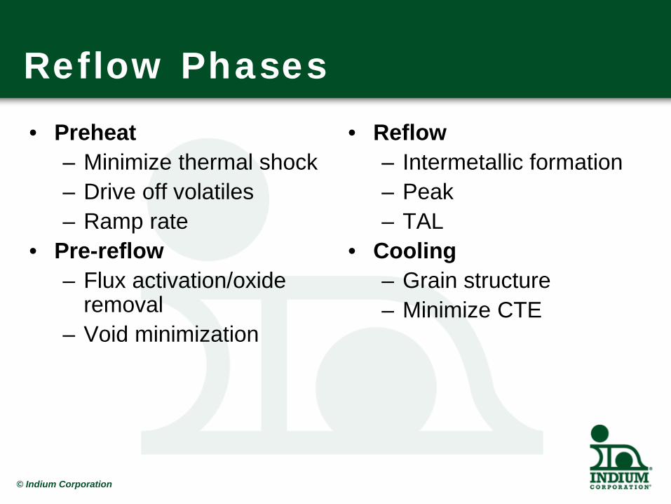
Reflow Phases • Preheat
– Minimize thermal shock – Drive off volatiles – Ramp rate
• Pre-reflow – Flux activation/oxide
removal – Void minimization
• Reflow – Intermetallic formation – Peak – TAL
• Cooling – Grain structure – Minimize CTE
© Indium Corporation
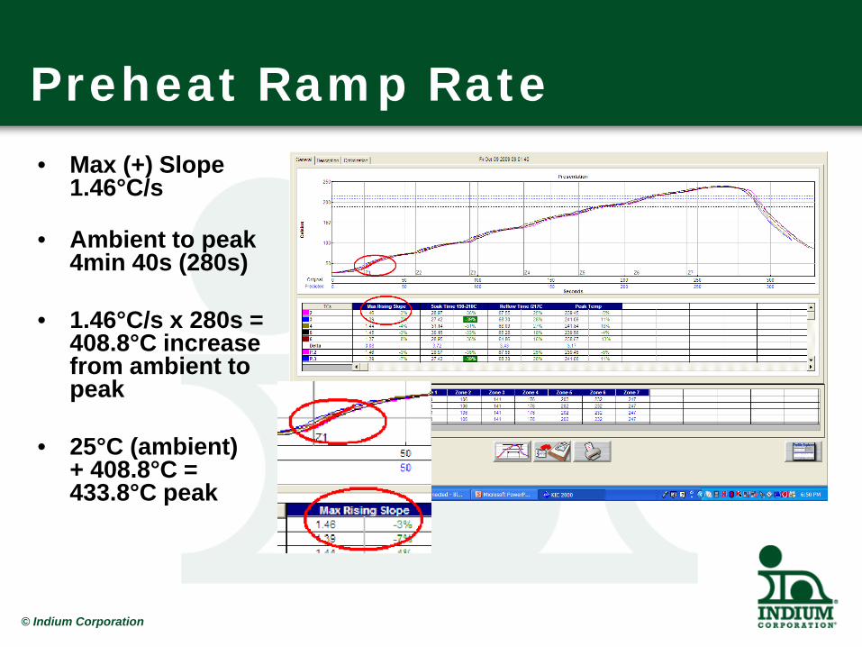
Preheat Ramp Rate • Max (+) Slope
1.46°C/s
• Ambient to peak 4min 40s (280s)
• 1.46°C/s x 280s = 408.8°C increase from ambient to peak
• 25°C (ambient) + 408.8°C = 433.8°C peak
© Indium Corporation
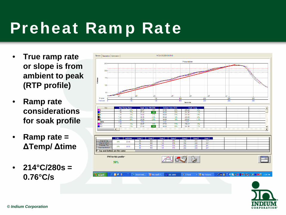
Preheat Ramp Rate • True ramp rate
or slope is from ambient to peak (RTP profile)
• Ramp rate considerations for soak profile
• Ramp rate = ΔTemp/ Δtime
• 214°C/280s = 0.76°C/s
© Indium Corporation

Factors Affecting Reflow Process Window • Water soluble vs. RMA/no-clean • Powder type • Board size • Component density/diversity
© Indium Corporation
Solder Defects
• Tombstoning • Solder Balling/Beading • Voiding • Graping • Head-in-Pillow (HIP)
© Indium Corporation
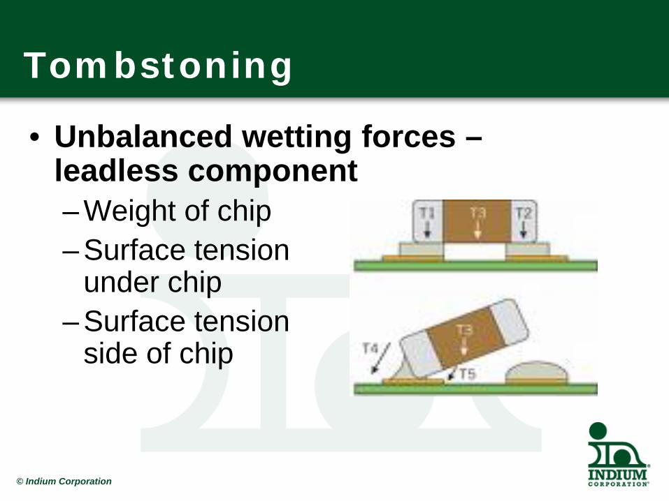
Tombstoning
• Unbalanced wetting forces – leadless component – Weight of chip – Surface tension
under chip – Surface tension
side of chip
© Indium Corporation
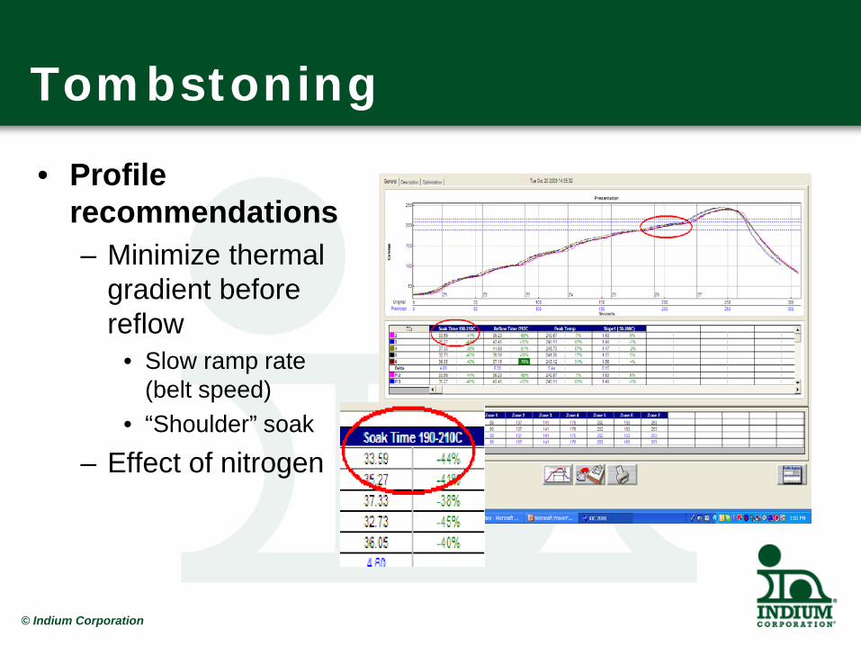
Tombstoning
• Profile recommendations – Minimize thermal
gradient before reflow
• Slow ramp rate (belt speed)
• “Shoulder” soak
– Effect of nitrogen
© Indium Corporation
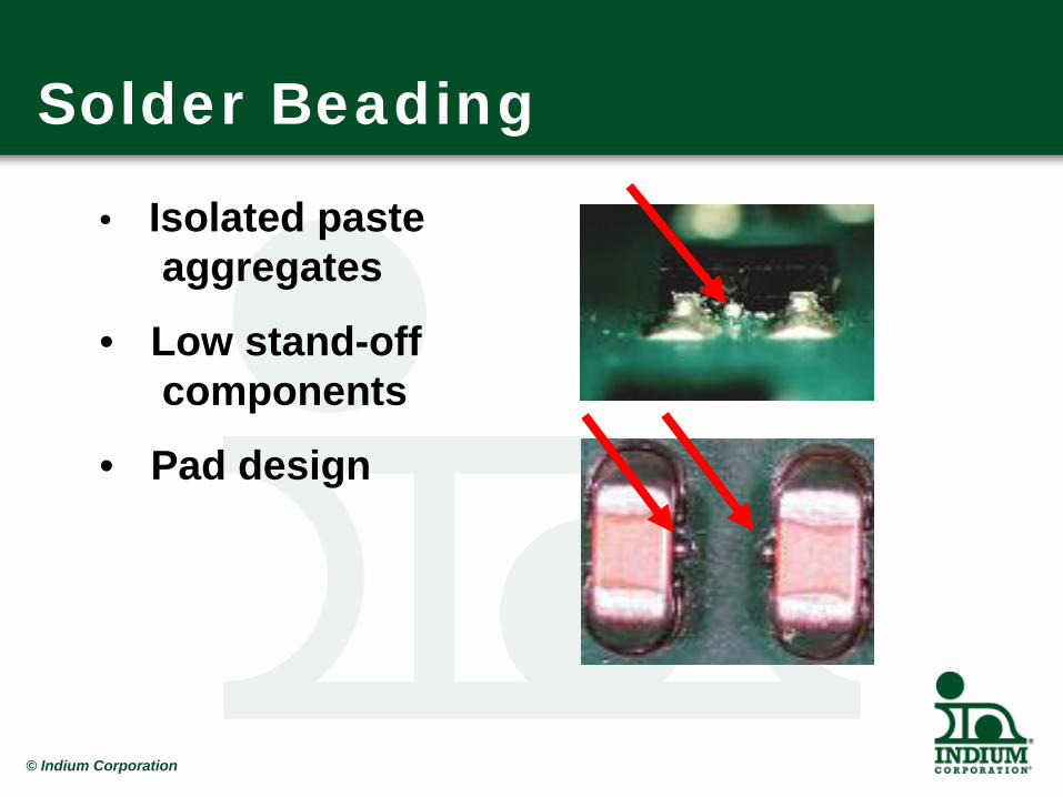
Solder Beading
• Isolated paste aggregates
• Low stand-off components
• Pad design
© Indium Corporation
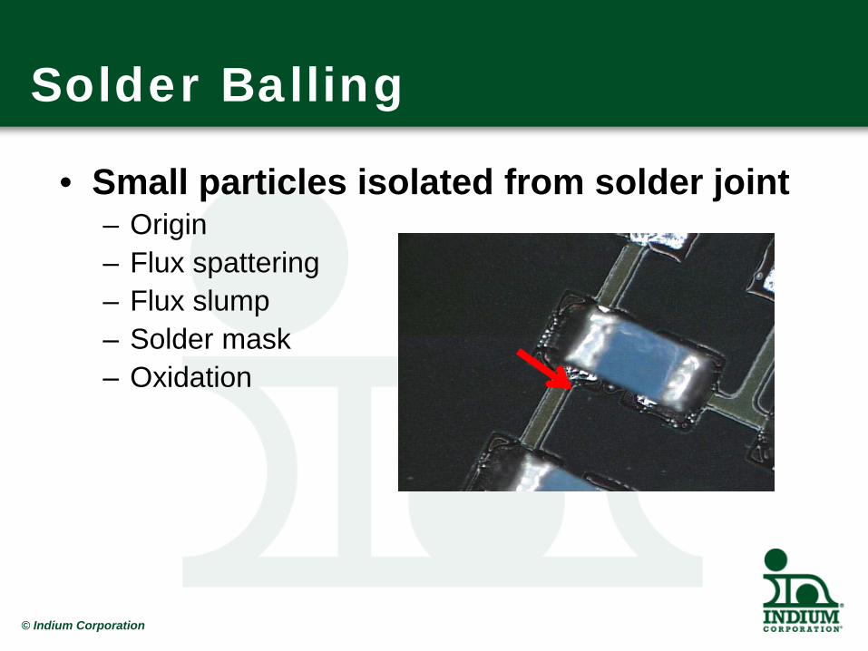
Solder Balling
• Small particles isolated from solder joint – Origin – Flux spattering – Flux slump – Solder mask – Oxidation
© Indium Corporation
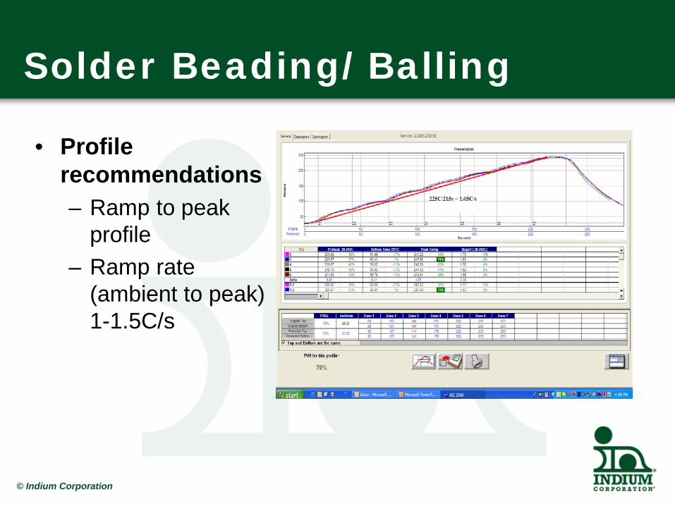
Solder Beading/Balling
© Indium Corporation
• Profile recommendations – Ramp to peak
profile – Ramp rate
(ambient to peak) 1-1.5C/s
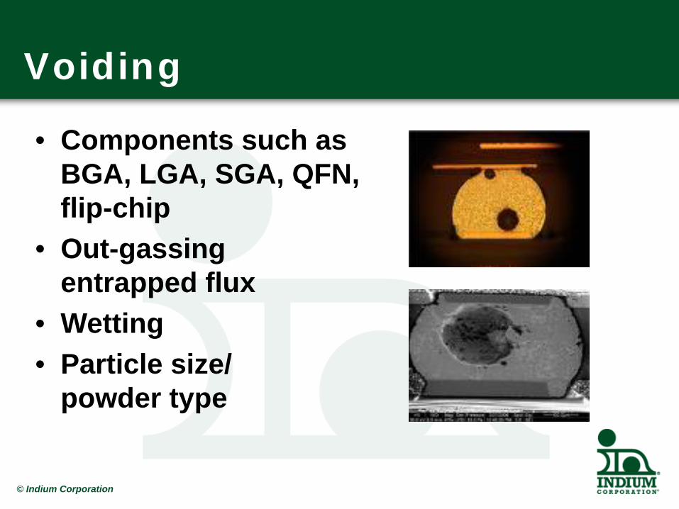
Voiding
© Indium Corporation
• Components such as BGA, LGA, SGA, QFN, flip-chip
• Out-gassing entrapped flux
• Wetting • Particle size/
powder type
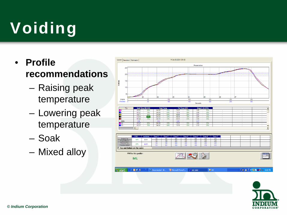
Voiding
© Indium Corporation
• Profile recommendations – Raising peak
temperature – Lowering peak
temperature – Soak – Mixed alloy
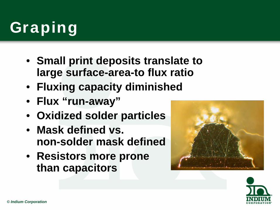
Graping
© Indium Corporation
• Small print deposits translate to large surface-area-to flux ratio
• Fluxing capacity diminished • Flux “run-away” • Oxidized solder particles • Mask defined vs.
non-solder mask defined • Resistors more prone
than capacitors
Graping
© Indium Corporation
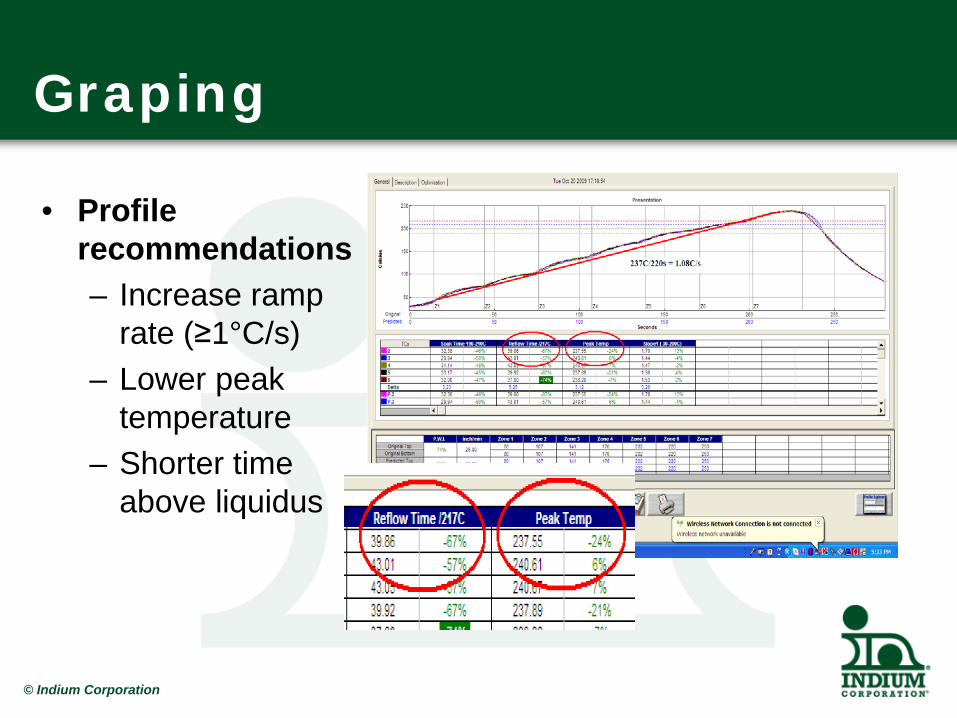
• Profile recommendations – Increase ramp
rate (≥1°C/s) – Lower peak
temperature – Shorter time
above liquidus
Head-in-Pillow
© Indium Corporation
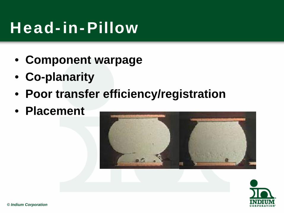
• Component warpage • Co-planarity • Poor transfer efficiency/registration • Placement

Head-in-Pillow
© Indium Corporation
• Sphere oxidation • Contaminants • Flux exhaustion
Head-in-Pillow
© Indium Corporation
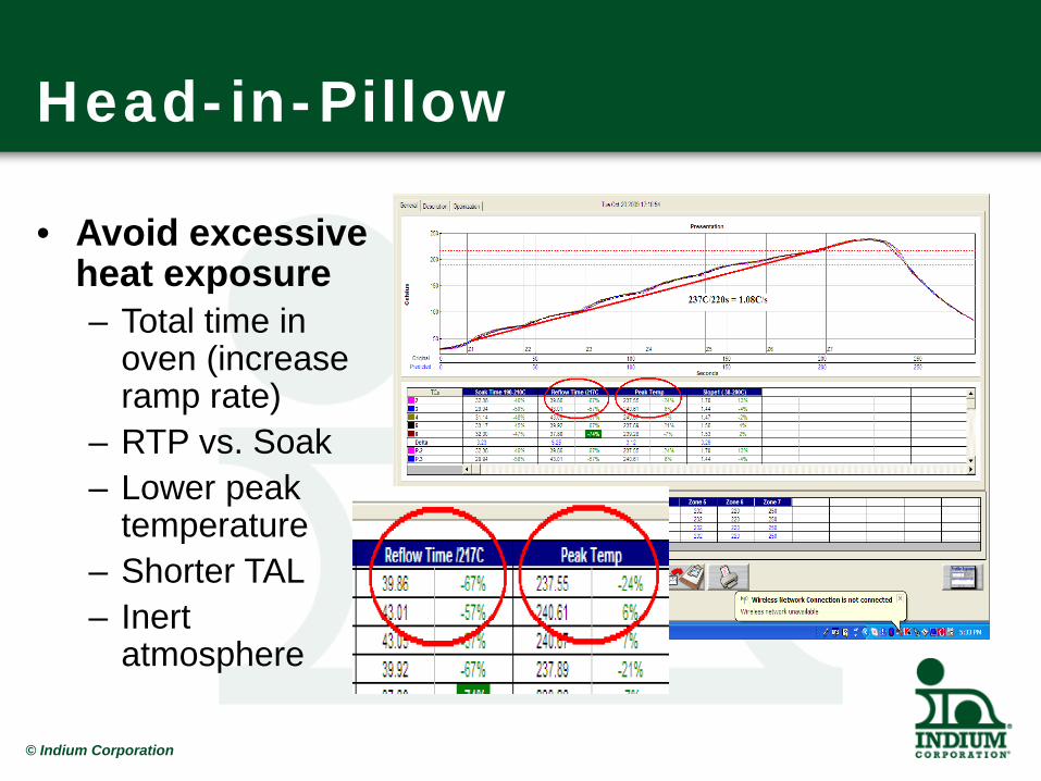
• Avoid excessive heat exposure – Total time in
oven (increase ramp rate)
– RTP vs. Soak – Lower peak
temperature – Shorter TAL – Inert
atmosphere
Conclusion
© Indium Corporation
• Lead-free challenges on solder paste • Understanding reflow profile • Optimizing the reflow process


