124


Contents
Messages: i-vi
From Convener: 1
From Scientific Program Committee: 2
Technical Program: 3 - 16
Abstracts of Invited Tutorial Talks: 17 - 19
Abstracts of Invited Review Talks: 20 - 36
Abstracts of Invited Paper Talks: 37 - 66
Abstracts of Oral Presentations: 67 - 74
Abstracts of Theses Presentations: 75 - 80
Abstracts of Poster Presentations: 81 - 122

FROM THE CONVENER….
Dear Invitees, Participants, Colleagues and Friends,
It gives me immense pleasure to welcome you all at the DAE BRNS 4th National Symposium on Pulsed Laser Deposition of Thin Films and Nanostructured Materials, PLD 2007 for short. Since its inception in 2001 biennial PLD meets have provided a forum for intense professional interactions amongst scientists, students and suppliers of the Indian PLD community. Countless ideas have been discussed, collaborations have been planned and executed, suggestions have been mooted and contemplated and an enormous amount of scientific knowledge has been disseminated and absorbed through these meetings. At PLD meets researchers from national laboratories and universities come closer to share their respective strengths and do away with their respective lacunae. We are indeed indebted to DAE – BRNS for their continued support to hold these meetings and hence to fulfill the purpose of these meetings. Albeit in a small way, PLD 2007 is witnessing something special that for sure is a reason for all of us to feel upbeat. Not only that we have registered a quantitative increase in the number of abstracts submitted, we notice a qualitative improvement of the research being presented in the papers. Not only that we have delegates from all the important institutes of the country, for the first time, we have a sizable participation of highly acclaimed scientists from Germany and China. These are harbingers of an upward contribution that Indian scientists are vying to make and enhancing integration of our research with the global science. Individually our forward moving steps may still be small but collectively we can proceed at a gallop. This is the goal we will strive to achieve together. As you can see from the planned proceedings of PLD 2007, the sequences of presentations are so elaborate that it will make your cup of time overflow. But I believe you will welcome this. By the time we wind up this meet, although we all will be extremely tired but will also be extremely happy to get soaked with new knowledge, new ideas and something significant to take home. I wish you all a very successful and enchanting participation in PLD 2007.
Lalit M. Kukreja August 20, 2007
1

FROM THE SCIENTIFIC PROGRAM COMMITTEE…
We take this opportunity to welcome you all to the PLD-2007 symposium. It is a great pleasure to share with you the feeling of overwhelming response of abstract submissions in this symposium. We have received about 85 abstract for PLD 2007 from most of the active groups from Indian Laboratories and some foreign participants from China and Germany. The number of total submitted abstracts in PLD 2007 is significantly higher than the total number of abstract received in previous PLD symposia e.g., in 28 in PLD-2005, 26 in PLD-2003 which and 19 in PLD-2001. The scientific standard of the contributed abstract has also improved significantly over the years. This year we received abstracts for thesis presentations also and included it in scientific program. The scientific programs will run all the three days and every day there will be different sessions of presentations such as invited tutorial talks (ITT), Invited review talks (IRT), Invited Paper talks (IPT), Oral presentations (OPT), thesis presentations (THP) and poster presentations (PSP).We have included a special session for corporate presentations on the last day of the symposium. In this session discussions about scientific products pertinent to the scope of the symposium will be carried out. An arrangement to display the product catalogues and handouts etc from the corporate sector have been made at the venue for all the three days. We thank Prof. L. M. Kukreja, Symposium Convener for his constant guidance and suggestions for preparing this compendium of abstracts. We would also like to thank our colleague Mr. Amit K. Das of RRCAT, Indore for his help in designing the cover pages of the abstract book. Thanks are also due to Dr. B. N. Singh of RRCAT, Indore and Mr. R. Bankar of Pune University, Pune for their help during preparation of the abstract book. We wish you all a very fruitful participation in PLD 2007 and happy back home.
Pankaj Misra Kiran P. Adhi Secretary Convener
Scientific Program Committee PLD-2007
2

October 2, 2007 (Tuesday) 20:00 hrs onwards: Welcome Dinner and Registration at Hotel Rangoli Park, Rajkot
Scientific Program
Venue: Resort Chouki Dhani, Rajkot
October 3, 2007 (Wednesday) Time 8:30-
9:30 9:30- 10:30
10:30-11:00
11:00-13:00
13:00-14:00
14:00-15:00
15:00-15:30
15:30-16:30
16:30-17:30
17:30-18:30
19:00-21:00
Sessions
Break Fast & Registration
Inauguration of the symposium
High Tea
IRT1 IRT2 IRT3 IRT4
Lunch ITT1 OPT1OPT2
Tea + PSP1
IPT1 IPT2
THP1 THP2
Cultural Program and Dinner
October 4, 2007 (Thursday) Time 8:30-
9:00 9:00 –
11:00 11:00- 11:30
11:30- 13:00
13:00-14:00
14:00-15:00
15:00-15:30
15:30-16:30
16:30-17:30
17:30-18:30
19:00- 21:00
Sessions
Break Fast & Registration
IRT5 IRT6 IRT7 IRT8
TEA IRT9IRT10 IRT11
Lunch ITT2 OPT3OPT4
Tea + PSP2
IPT3 IPT4
THP3 THP4
Dinner
October 5, 2007 (Friday) Time 8:30-
9:00 9:00 –
11:00 11:00- 11:30
11:30- 13:00
13:00-14:00
14:00-15:00
15:00-15:30
15:30-16:00
16:00-17:30
17:30- 19:00
19:00-21:00
Sessions
Break fast
IRT12 IRT13 IRT14 IRT15
TEA IRT16IPT5 IPT6
Lunch ITT3 OPT5OPT6
TEA THP5IPT7 OPT7 OPT8
CPT1 CPT2 CPT3 CPT4 CPT5
Closing and Dinner
ITT: Invited Tutorial Talk; IRT: Invited Review Talk; IPT: Invited Paper Talk; OPT: Oral Presentation; THP: Theses Presentation; PSP: Poster Presentation CPT: Corporate Presentation Time durations: ITTs: 60 min; IRTs: 30 min; IPTs: 30 min; OPT: 15 min; THPs: 30 min; CPTs: 15 min
3

Invited Tutorial Talks (ITT) S.
No. Code No.
Title Speaker Address
Co-authors
1 ITT1 Optical Properties of Semiconductors at the fundamental absorption edge
Claus Klingshirn
Institut für Angewandte Physik Universität Karlsruhe Karlsruhe Germany Claus.Klingshirn@ physik.uni-karlsruhe.de
J. Fallert, H. Zhou, and H. Kalt
2 ITT2 Field Emission From Nanomaterials - A Tutorial
D. S. Joag Centre for Advanced Studies in Condensed Matter Physics and Material Science Department of Physics Pune University Pune 411 007 [email protected]
3 ITT3 Pulsed Laser Growth of Nanostructured Materials: Some Recent Experiments
L. M. Kukreja Thin Film Laboratory, RRCAT, Indore – 452 013 [email protected]
Invited Review Talks (IRT)
S.
No. Code No.
Title Speaker Address Co-authors
4 IRT 1
Research on p-type ZnO
Z. Z. Ye State Key Laboratory of Silicon Materials, Zhejiang University, Hangzhou, 310027, E-mail: [email protected]
Y. F. Lu, Y. J. Zeng, J. G. Lu, L. P. Zhu
5 IRT 2
Electrical, Optical And Magnetic Properties Of Oxide Based Nanostructures
M. S. Ramachandra Rao
Department of Physics, Indian Institute of Technology, Madras, Chennai [email protected]
6 IRT 3
Temperature-dependent photoluminescence from ZnO/Zn0.85Mg0.15O quantum well grown on Si(111) substrates
L.P. Zhu State Key Lab of Silicon Materials, Department of Materials Science and Engineering, Zhejiang University, Hangzhou, 310027, People’s Republic of China [email protected]
X.Q. Gu, H.P. He, F. Huang, M.X. Qiu, Z.Z. Ye, Y.Z. Zhang, B.H. Zhao
7 IRT 4
Electron doped manganites: Reality or illusion?
Pratap Raychaudhuri
Department of Condensed Matter Physics and Materials Science,TIFR,, Homi Bhabha Rd., Colaba, Mumbai-400005
4

8 IRT 5
Multiferroic behavior of modified BiFeO3 thin films grown by PLD: A Review
V. R. Palkar Electrical Engineering, Indian Institute of Technology Bombay, Mumbai 400 076, India [email protected]
9 IRT 6
Nanostructured Thin Films of Titania Prepared by Pulsed Laser Ablation: Process and Properties
P. Kuppusami
Physical Metallurgy Division Indira Gandhi Centre for Atomic Research Kalpkkam-603 102, Tamilnadu [email protected]
S. Murugesan and E. Mohandas
10 IRT 7
Combinatorial Pulsed Laser Abltation for Parallel Synthesis and High Throughput Characterization of Functional Inorganic materials
Utpal S. Joshi
Department of Physics, School of Sciences, Gujarat University, Ahmedabad–380009 [email protected]
11 IRT 8
Single Step Single Shot Lithography Techniques via Selective laser ablation
Alika Khare
Department of Physics Indian Institute of Technology Guwahati, Guwahati 781039 [email protected]
12 ITR 9
Pulsed laser deposition of amorphous oxides for transparent electronics
M.K. Jayaraj
Optoelectronic Devices Laboratory, Department of Physics, Cochin University of Science and Technology, Kochi 682 022 [email protected]
K.J. Saji
13 IRT 10
Preparation of Luminescent Nanostructures by Pulsed Laser Ablation
V.P.Mahadevan Pillai
Department of Optoelectronics, University of Kerala, Kariavattom, Kerala, India [email protected]
14 IRT 11
Studies on manganite based Thin films and Heterostructures grown by PLD
D. G. Kuberkar
Department of Physics, Saurashtra University Rajkot- 360 005 Gujarat [email protected]
15 IRT 12
Laser ablation of Zn/ZnO Core-Shell Nanoparticles: Effect of SDS Concentration
R. K. Soni
Laser Spectroscopy Laboratory, Physics Department Indian Institute of Technology, Delhi, New Delhi-110016 [email protected]
First author: Geetika Bajaj
5

16 IRT 13
Characterization of pulsed laser deposited Fe3O4 thin films on different substrates
D. M. Phase UGC-DAE Consortium for Scientific Research, University Campus, Indore-452017, India. [email protected]
17 IRT 14
Application of pulsed laser deposited thin films of ZnO as varistors and InN as field emitters
K. P. Adhi Center for Advanced Studies in Material Science and Condensed Matter Physics. DST unit on Nanoscience, Department of Physics, University of Pune, Pune –411 007, India [email protected]
18 IRT 15
Effect of swift heavy ion irradiation on the surface morphology of highly c-axis oriented LSMO thin films grown by pulsed laser deposition.
S. I. Patil Department of Physics, University of Pune, Pune 411 007
in
M. S. Sahasrabudhe,
Deepak N. Bankar, A. G. Banpurkar and
K. P. Adhi
19 IRT 16
Tailoring the electrical and magnetic properties of LaFe1-xNixO3 thin films by swift heavy ion irradiation
Ravi Kumar Inter University Accelerator Centre, Aruna Asaf Ali Marg, New Delhi-110067 [email protected]
Invited Paper Talks: (IPT)
S. No.
Code No.
Title Speaker Address Co-authors
20 IPT1 Study of device characteristics on Pulsed Laser Deposited manganite-semiconductor heterostructures
S.N. Kale Fergusson College Pune 411 004, India [email protected]
J. Mona, H. Mamgain, R.R. Rawat, V. Ganesan, R.J. Choudhary, D.M. Phase
21 IPT2 Pulsed Laser Deposition of La1.5Dy0.5CaBa2Cu5Oz Superconducting Thin Films
S. Rayaprol UGC-DAE CSR-Mumbai centre, R-5 Shed, BARC, Trombay, Mumbai [email protected] [email protected]
K. R. Mavani, D. G. Kuberkar, N. A. Shah, J. John, R. Pinto
22 IPT3 Basic Photoluminescence Processes at different Temperatures in ZnO / (0001) Sapphire Thin Films Grown by Pulsed
P. Misra Laser Program, Raja Ramanna Centre for Advanced Technology, Indore– 452 013 (M.P.)
T. K. Sharma and L. M. Kukreja
6

Laser Deposition [email protected]
23 IPT4 Synthesis and properties of pulsed laser deposited Fe doped MoO3-d thin films
R. J. Choudhary UGC-DAE Consortium for Scientific Research, University Campus, Indore-452017, India. [email protected]
Ram Prakash, D. M. Phase and Ravi Kumar
24 IPT5 UV Excimer lasers for smart materials and nanostructures
B. Fechner Coherent GmbH, Hans-Böckler-Str. 12, D-37079 Göttingen, Germany [email protected]
R. Pätzel, R. Delmdahl
25 IPT6 Precise photonic engines for UV pulsed laser deposition
R. Delmdahl Coherent GmbH, Hans-Böckler-Str. 12, D-37079 Göttingen, Germany [email protected]
J. Sieber, B. Fechner
26 IPT7 Research and Development in Pulsed Laser Deposition: A Scientometric Perspective
G. Surwase Scientific Information Resource Division, Knowledge Management Group Bhabha Atomic Research Centre, Mumbai-400 085 (India) [email protected]; [email protected]
B.S. Kademani and Vijai Kumar
Oral presentations: (OPT)
S. No.
Code No.
Title Speaker Address Co-authors
27 OPT1 Large Room Temperature Magnetization of Pulsed Laser Deposited Cobalt Ferrite Thin Film
Subasa C. Sahoo
Department of physics,Indian Institute of Technology Bombay Powai, Mumbai – 400076 [email protected]
M. Bohra, N.Venkataramani, Shiva Prasad, D. S. Misra and R. Krishnan
28 OPT2 Photoluminescence of ZnO nanowires grown by thermal evaporation on pulsed laser deposited ZnO buffer layer
A. Mohanta Department of Physics and Centre for Laser Technology, Indian Institute of Technology Kanpur-208016 [email protected]
A. P. Singh, Vandna S., and R. K. Thareja
29 OPT3 Nanostructured Growth of AlN Thin Films by Pulsed Laser Deposition
Gaurav Shukla Department of Physics Indian Institute of Technology Guwahati, Guwahati 781039 [email protected]
Alika Khare
30 OPT4 Resistivity of thin films of YBa2Cu3O7-δ and
L.S.Vaidhyanat-han
Materials Science Division, Indira Gandhi Centre for
D.K. Baisnab, M.P.
7

Multilayers of YBCO/Ga2O3
Atomic Research, Kalpakkaam [email protected]
Janawadkar and Y. Hariharan
31 OPT5 Morphological and physical property changes in ZnO thin films grown by PLD due to Mg doping
Shubra Singh Department of Physics and Materials Science Research Centre IIT Madras, Chennai-36, India [email protected]
M. S. Ramachandra Rao
32 OPT6 Characteristics of pulsed laser deposited Zn1-
xNixO/ZnO bi-layer thin films
Subhash Thota Materials Science Programme, Indian Institute of Technology Kanpur, Kanpur-208016 [email protected]
Pankaj Misra, Lalit M Kukreja and Jitendra Kumar
33 OPT7 Structural and Optical Characterization of UV-transparent β-Ga2O3
V. Sridharan Material Science Division, Indira Gandhi Centre for Atomic Research, Kalpakkam 603102. [email protected]
L.S. Vaidhyanathan, V. Srihari, G. Raghavan, S. T. Sundari, M. Kamruddin, M. Premila, H.K. Sahu, B. K. Panigrahi, V.S. Sastry and C.S. Sundar
34 OPT8 The low temperature electrical transport in La0.7Ca0.3MnO3
P.R. Sagdeo UGC-DAE Consortium for scientific research, University campus Khandwa road indore 452017, M.P. INDIA [email protected]
R.J. Choudhary and D.M. Phase
Thesis Presentations: (THP)
S.
No. Code No.
Title Speaker Address Co-authors
35 THP1 Oxygen Reduction Kinetics and Transport Properties of (Ba,Sr)(Co,Fe)O3-delta Solid Oxide Fuel Cell Cathode Materials
Lei Wang Max Planck Institute for Solid State Research, Heisenbergstrasse 1, D-70569 Stuttgart, Germany [email protected]
Rotraut Merkle1, Frank S. Baumann1, Jürgen Fleig2, and Joachim Maier1
36 THP2 Study on p-type ZnO thin films and ZnO homojunction LED
Y. Lu State Key Laboratory of Silicon Materials, Zhejiang University, Hangzhou, 310027, People’s Republic of China [email protected]
Z. Z. Ye, Y. J. Zeng, L. P. Zhu
37 THP3 Magnetoresistive and Jaysukh H Department of Physics,
8

Transport Properties of Pulsed Laser Deposited Manganite Thin Films and Heterostructure.
Markna Saurashtra University, Rajkot-360 005 INDIA [email protected]
38 THP4 Pulsed Laser Deposited Thin Films of ZnO, GaN, AlN, ZnO/GaN WBSC: Structural, Micro-structural, Optical & Electrical Characterization
Suhas Madhav Jejurikar
Center for Advanced Studies in Materials Science and Condensed Matter Physics, Department of Physics, University of Pune, Pune 411 007, India. [email protected]
Dr. K. P. Adhi, Co-guide: Dr. A. V. Limaye
39 THP5 Synthesis and characterization of LaB6 thin films on tungsten, rhenium and silicon substrates and their investigations as Field Emitters
D. J. Late Center for Advanced Studies in Material Science and Condensed Matter Physics, Department of Physics, University of Pune, Pune - 411007, India [email protected]
Poster Presentations: (PSP) PSP 1 (October 3, 2007)
S. No.
Code No.
Title Speaker Address Co-authors
40 PSP1.1
Effect of oxygen pressure on the photoluminescence of Gd2O3 :Eu 3+ films grown by PLD
Geo Rajan
Department of Optoelectronics, University of Kerala, Kariavattom, Thiruvananthapuram-695 581, India [email protected]
Nissamudeen K. M, Sasi B
and K.G.Gopchand
ran
41 PSP1.2
A comparative study of nanostructures Co thin films deposited on different substrates by pulsed laser deposition
A. Sharma University Grant Commission- Department of Atomic Energy Consortium for Scientific Research, University Campus, Khandwa Road, Indore-452 017, India. [email protected]
S. Tripathi, R. Brajpuriya, Ram Prakash, R. J. Chaudhari, D. M. Phase and T. Shripathi
42 PSP1.3
Raman Study of oriented thin films of PrMnO3 deposited on different
Aditi Dubey UGC-DAE Consortium for Scientific Research, University Campus, Khandwa
V. G. Sathe
9

substrates Road, Indore – 452 017 [email protected]
43 PSP1.4
Application of pulsed laser deposited ZnO thin films as a solar blind detector
Alka V. Deshmukh
Center for Advanced Studies in Materials Science and Condensed Matter Physics, Department of Physics, University of Pune, Pune 411 007, India. [email protected]
S. M. Jejurikar, K. P. Adhi and S. I. Patil
44 PSP1.5
DC-Discharge Assisted Pulsed Laser Growth of Ultra-thin Silicon-Oxinitride Films
B. N. Singh Thin Film Lab., Raja Ramanna Centre for Advanced Technology, Indore 452 013 [email protected]
P. Misra, A. K. Das, R. Kumar, Binsu J Kailath, M. Mishra, D.M. Phase, A. DasGupta, N. DasGupta and L. M. Kukreja
45 PSP1.6
Unique nanostructures in pulsed laser ablated NiO thin films
B. Sasi Department of Optoelectronics, University of Kerala, Thiruvananthapuram-695 581, India [email protected]
K.M. Nissamudeen and K. G. Gopchnadran
46 PSP1.7
Influence of Ti2+ doping on the structural and optical properties of WO3 thin films prepared by pulsed laser ablation technique.
Lethy K.J Department of Optoelectronics, University of Kerala, Kariavattom, Kerala, India [email protected]
Beena D, Bahna.A.H V.P.Mahadevan Pillai
47 PSP1.8
Effect of Substrate on Pulsed Laser Deposition of InN Thin Film
Gaurav Shukla Department of Physics Indian Institute of Technology Guwahati, Guwahati 781039 [email protected]
Alika Khare
48 PSP1.9
Synthesis and Optical Properties of Cr2O3 Films Prepared by Pulsed Laser Ablation
G. Balakrishnan Physical Metallurgy Division, Indira Gandhi Centre for Atomic Research, Kalpakkam-603 102, Tamil nadu [email protected]
P. Kuppusami, T.N. Sairam, E. Mohandas and D. Sastikumar
49 PSP1.10
Synthesis and Characterization of La0.7Ba0.3MnO3-SnO2 bilayer using Pulsed Laser Deposition Technique
J. Mona Fergusson College, Fergusson College Road, Pune 411004 [email protected]
Ram Prakash, R. Rawat, R.J. Choudhary, D.M. Phase, S.N. Kale
10

50 PSP1.11
Semiconductor Nano-pattern formation through laser induced diffusion
U. Das Dept of Physics, Tezpur University, Napaam, Tezpur – 784028, India [email protected]
A.Choudhury
51 PSP1.12
Growth of n-Zinc Oxide on various substrates using pulsed laser deposition and its photo conducting properties
G. Naresh Kumar
Loyola institute of frontier energy (LIFE), Physics Department, Loyola college, Chennai 600 034, India [email protected]
V.Immanuel, Francis P. Xavier
52 PSP1.13
Characterisation of pulsed laser deposited PZT and PLZT thin films on oxide pervoskite electrodes
R.Reshmi Optoelectronics Device Laboratory, Department Of Physics, Cochin University of Science and Technology, Kochi-682022, India [email protected]
M.K.Jayaraj, M.T.Sebastian
53 PSP1.14
Effect of Structural Disorder on Electronic Transport in La0.5Pr0.2R0.3MnO3 (R = Sr, Ba) Manganite Thin Films
P.S. Solanki Department of Physics, Saurashtra University, Rajkot – 360 005 [email protected]
R.R. Doshi, J.H. Markna, C.M. Thaker, N.A. Shah and D.G. Kuberkar K.R. Mavani, D.S. Rana and S.K. Malik P. Misra, B.N. Singh and L.M. Kukreja
54 PSP1.15
Improvement in field sensitivity of La-based manganite multilayered structure
P.S. Vachhani Department of Physics, Saurashtra University, Rajkot – 360 005, India [email protected]
J.H. Markna, J.A. Bhalodia and D.G. Kuberkar P. Misra, B.N. Singh and L.M. Kukreja V. Ganesan and R. Rawat
55 PSP1.16
Synthesis and Characterization of PrCoO3 thin films grown by Pulsed Laser Deposition
Ram Prakash UGC-DAE Consortium for Scientific Research, Indore (M.P.) 452017, India. [email protected]
R. J. Choudhary, D. M. Phase
56 PSP1.17
Effect of laser energy on the structural and optical properties of non-reactive pulsed laser ablated tantalum oxide thin films
Renju R Krishnan
Department of Optoelectronics, University of Kerala, Kariyavattom, Trivandrum-695581, Kerala, INDIA [email protected]
V.P.M. Pillai
57 PSP1.18
Room temperature luminescence from low temperature grown ZnMgO/ZnO Quantum wells using pulsed laser deposition.
R.S. Ajimsha Optoelectronics Devices Laboratory, Department
of Physics, Cochin University of
Science and Technology, Cochin-22.
M.K.Jayaraj
P Misra, L.M. Kukreja
58 PSP1.19
Novel feature of quantum transport through finite
Santanu K. Maiti
1Theoretical Condensed Matter Physics, Saha Institute
11

width mesoscopic ring
of Nuclear Physics, 1/AF, Bidhannagar, Kolkata-700 064, India
59 PSP1.20
Structural, Optical and Electrical Properties of Co and Ga codoped ZnO Thin Films Prepared by Pulsed Laser Deposition
M. Subramanian Crystal Growth Centre, Anna University, Chennai – 600 025 [email protected]
G. Mohan Kumar, P. Misra. Amit K Das, B. N. Singh, S. Venkatraj, S. Vijayalakshmi, R. Jayavel and L.M. Kukreja
PSP2 (October 4, 2007)
60 PSP2.1
Structural, Optical and Electrical Properties of Zn1-(x+y)MnxGayO THIN FILMS Prepared by Pulsed Laser Deposition
M. Subramanian Crystal Growth Centre, Anna University, Chennai – 600 025
P. Ilanchezhiyan, P. Misra. A. K Das, B. N. Singh, S. Venkatraj, S. Vijayalakshmi, R. Jayavel and L.M. Kukreja
61 PSP2.2
Effect of doping and substrate temperature on the structural and optical properties of reactive pulsed laser ablated Aluminium Oxide doped Tantalum Oxide thin films
Renju R Krishnan
Department of Optoelectronics, University of Kerala, Kariavattom, Trivandrum-695581, Kerala, INDIA. [email protected]
V.P.M. Pillai
62 PSP2.3
Optimizing the doping concentration in a single experiment by using Combinatorial Laser Molecular Beam Epitaxy (CLMBE)
Utpal S. Joshi Department of Physics, School of Sciences, Gujarat University, Ahmedabad – 380 009, India usjoshi@gmail com
Kenji Itaka, Yuji Matsumoto, Masatomo Sumiya and Hideomi Koinuma
63 PSP2.4
Superparamagnetism in epitaxial thin films of Fe, Cr, Co, Mn and V doped p-type NiO
U. V. Chhaya Physics Department, St. Xavier’s College, Ahmedabad-380 009, India usjoshi@gmail com
P.S. Raval, P.A. Joshi, S. Trivedi, K. Itaka, Y.Matsumoto, H. Koinuma and U.S. Joshi
64 PSP2.5
Structural and Optical properties of GdO doped ZnO Thin Films by Pulsed Laser Deposition Technique.
R.Vinodkumar Department of Optoelectronics, University of Kerala, Thiruvananthapuram, Kerala, India – 695581. [email protected]
D.Beena, Geo Rajan, Jayasree R.S. and V.P.Mahadevan Pillai
65 PSP2.6
Structural, Morphological and Optical studies of Potassium Lithium Niobate thin films prepared under ambient conditions of substrate temperature
V. Jayasree Department of Optoelectronics, University of Kerala, Kariavattom, Trivandrum, Kerala, 695 581 India
R Vinod Kumar, R Ratheesh, V. P Mahadevan Pillai & V. U Nayar
12

66 PSP2.7
Studies on effect of europium concentration on the photoemission of laser ablated Y2O3:Eu based nano-phosphors.
K.M. Nissamudeen
Department of Optoelectronics, University of Kerala, Kariavattom, Thiruvananthapuram [email protected]
R Krishnan, Geo Rajan and K.G. Gopchandran
67 PSP2.8
Studies on Si Doped ZnO Thin Films Grown by Sequential Pulsed Laser Deposition
A.K. Das Thin Film Laboratory, Raja Ramanna Centre for Advanced Technology, Indore 452 013 [email protected]
B. N. Singh, P. Misra and L. M. Kukreja
68 PSP2.9
Textured CeO2 thin films on amorphous substrate by PLD at room temperature
T. K. Chaudhuri
Dr. K C Patel Research and Development Centre Education Campus – Changa, Changa (Petlad), Anand Gujarat 388 421, INDIA [email protected]
R N Bhattacharya
69 PSP2.10
Synthesis of II-VI Oxide Semiconductor Nanocrystals by Pulsed Laser Ablation in Liquid Media
S. C. Singh Laser and Spectroscopy Laboratory, Department of Physics, University of Allahabad, Allahabad-211002 [email protected]
R.K. Swarnkar and R. Gopal
70 PSP2.11
Studies on CoZnO thin films grown by Pulsed Laser Deposition
Satyapal S. Rathore
Dept. of Applied Physics, Birla Institute of Technology, Mesra – 835215 and Thin Film Laboratory, Raja Ramanna Centre for Advanced Technology, Indore 452 013 [email protected]
A.K.Das, B.N. Singh, P.Misra, L.M.Kukreja
71 PSP2.12
Laser assisted growth of Eu3+ doped Ba0.7Sr0.3TiO3 thin film for optoelectronic and ferroelectric application
R.Reshmi Optoelectronics Device Laboratory, Department Of Physics, Cochin University of Science and Technology, Kochi-682022, India [email protected]
M.K.Jayaraj, M.T.Sebastian
72 PSP2.13
Comparative studies of irradiation induced modifications in Fe3O4 thin films on MgO and Si substrates grown by pulsed laser ablation
Shailja Tiwari UGC-DAE Consortium for Scientific Research, Indore-452 017, INDIA email: [email protected]
Ram Prakash, R. J. Choudhary and D. M. Phase Ravi Kumar
73 PSP2.14
Synthesis and Characterization of SnO2 Thin Films by PLD for Sensor Applications
K. Prabakar Materials Science Division, Indira Gandhi Centre for AtomicResearch, Kalpakkam – 603102,Tamil Nad [email protected]
R. Krishnan, B. Yasodhaadevi, Ashok S. Chauhan, S. Tripura Sundari, S. Dash and J. Jayapandian
13

74 PSP2.15
Structural and electrical characterization of pulsed laser deposited Ga doped ZnO thin films on Si(100)
S.D. Shinde Center for Advanced Studies in Materials Science and Condensed Matter Physics, Department of Physics, University of Pune, Pune 411 007, India. [email protected]
S.M. Jejurikar and K.P. Adhi
75 PSP2.16
Thickness dependent multiferroic properties of Bi0.7Dy0.3FeO3 polycrystalline thin films grown by pulse laser deposition technique
Prashanthi K Electrical Engineering, Indian Inof Technology Bombay, Mumba076, India [email protected]
S. P. Dattagupta, R. Pinto and V.
R. Palkar
76 PSP2.17
Electroresistive and Magnetoresistive effects in electron doped manganite La0.7Ce0.3MnO3 thin films
Kavita Bajaj Department of Condensed Matter Physics and Materials Sciences, TIFR, Homi Bhabha Rd., Colaba, Mumbai 400005, India. and Department of Physics, Mumbai University, Mumbai 400098, India. [email protected] [email protected]
John Jesudasan,
Vivas Bagwe, Pratap
Raychaudhuri
77 PSP2.18
Size dependent study of CuFe2O4 nanoparticles
Archana Rai Department of Physics, Indian Institute of Technology, Powai, Mumbai-400 076 [email protected]
M. Banerjee
78 PSP2. 19
A theoretical approach to the effect of particle size on the luminescence intensity in nanocrystals
Anamika Awadhwal
Department of Post Graduate Studies and Research in Physics and Electronics Rani Durgavati University, Jabalpur-482001
B.P. Chandra
79 PSP2. 20
Third Order Non-Linear Optical Properties of Eurhodin Dye Doped Ppolymer Film
Rekha R.K Centre for Laser Technology, Department of Physics, Anna University, Chennai-600 025 [email protected]
A. Ramalingam ,
G. Vinitha
80 PSP2.21
Nonlinear characterization and optical limiting of organic dye doped polymer
G.Vinitha Centre for Laser Technology, Department of Physics,Anna University, Chennai-25, India. [email protected]
R.K REKHA., A.
RAMALINGAM
81 PSP2.22
Studies on the Fluorescence emission from nano silver / silver oxide thin films for optical read write
A. Subrahmanyam
Department of Physics, Indian Institute of Technology Madras, Chennai-600036, India
N.Ravichandra Raju
14

memory applications
Corporate Talks: (CPT) S. No. Code
No. Company Speaker Address
82 CPT1 Oerlikon leybold Vacuum
S. Inamdar EL-22, J-Block, MIDC Bhosari, Pune-411 026 [email protected] www.oerlikon.com
83 CPT2. Laser Science L. Kumar Laser Science Services Pvt. Ltd. A-454, MIDC, TTC Industrial Area, Mahape, Navi Mumbai – 400 701 [email protected]
84 CPT3 Specialise Instruments Pvt. Ltd.
P. Deshpande Specialise Instrument Marketing Co. 18th Fort-view, Scheme No. 6, Road No.1, Sion (East), Mumbai 400 022, India [email protected]
85 CPT4 Excel Instruments S. P. Pai Excell Instruments A/15 Guru Nanak Compound Opp. Hindustan Lever, Chakala Road Andheri (East) Mumbai 400 099 [email protected]
86 CPT5 Laser Spectra Services India Pvt. Ltd.
N.R.P.Kumar
Laser Spectra Services India Pvt. Ltd., 80/10, I Floor, Raj Towers, M. S. Ramiah Main Road, Mathikere, BANGALORE-560 054. [email protected]
15

ITT1 Optical Properties of Semiconductors at the fundamental absorption edge
Claus Klingshirn, J. Fallert, H. Zhou, and H. Kalt
Institut für Angewandte Physik
Universität Karlsruhe 76128 Karlsruhe, Germany
email: [email protected] In this tutorial talk we review the optical properties of direct gap semiconductors and semiconductor quantum structures close to the fundamental absorption edge, using essentially ZnO as model substance. In a first part we start with the band structure, i.e. the one particle states, proceed to the electron-hole pair states i.e. the excitons and end this section with the mixed state of excitons and photons, the exciton polaritons. The second part will be devoted to the properties of and processes in a dense exciton or generally electron-hole pair system reaching the electron-hole plasma at the highest densities. Frequently, these processes allow stimulated emission and we spend the third part on this aspect.
16
ITT2
Field Emission From Nanomaterials - A Tutorial
DILIP S. JOAG
Centre for Advanced Studies in Condensed Matter Physics and Material Science University of Pune : Department of Physics
Field electron emission phenomenon is known for more than a century and is the best
example of quantum mechanical tunneling process. Since the invention of the field emission
microscope, it has been an important tool in the study of surface adsorption phenomena, work
function measurements, diffusion kinetics etc. The specimen in the field emission microscope is
required to be in the form of a sharp needle in order to create electric field of the order of 106 – 107
V/cm necessary for measurable emission current. Technologically, the phenomenon is important for
its potential application as a high brightness electron source.
In the era of nanomaterials, there has been renewed interest and an upsurge in the study of
field emission. This is due to the advantage of the size and shape of nanocrystallites of various
materials. These nanometeric materials become eligible candidates for `low onset voltage’ field
emitters. Several such materials have been investigated worldover for their potential applications in
field emission based devices such as flat panel displays.
This tutorial is aimed at giving the basic background required for the study of field emission
from nanomaterials. Various case studies will be presented illustrating the suitability of these
materials in the development of field emission cathodes and devices. Work from the author’s
laboratory on pulsed laser deposited nanometric films of ZnO and LaB6 will also be presented
elucidating the scope of the studies.
17

ITT3
Pulsed Laser Growth of Nanostructured Materials: Some Recent Experiments
L. M. Kukreja
Thin Film Laboratory, Raja Ramanna Centre for Advanced Technology,
Indore – 452 013
Email: [email protected]
In this tutorial talk results of our two ongoing experiments will be discussed. One experiment is on the behavior of sub-monolayer gold nano-islands grown on (0001) Sapphire substrates by Pulsed Laser Deposition (PLD). The other experiment is about a variant of PLD to grow ultra-thin high k-dielectric layer of SiO2 and silicon oxy-nitride for MOS technology. Nanometer size gold depositions on oxide substrates have recently come under scrutiny since the experimental observation of their large catalytic activity. Using high resolution Atomic Force Microscopy (AFM) we observed in normal ambient atmosphere the slow morphological dynamics of apparently sessile gold nano-islands grown on (0001) Sapphire substrates by Pulsed Laser Deposition (PLD) at room temperature with an equivalent average thickness of about 0.55 Å, i.e. one fourth of the monolayer. Within approximately one day, a transient wavy surface structure developed with rms roughness of about 0.6 nm and a two-fold symmetry. After about 6 days under ambient conditions this structure completely transformed into a de-wetted phase of spherical gold beads with average diameter of ~20 nm and a broad size distribution. Each bead was found to be surrounded by a concentric layer, which could be seen as corona in the AFM images. This concentric shell layer appears to be mainly the condensed moisture from atmosphere since by dehydration of the sample in vacuum using molecular sieves the corona layer completely vanished. While the shape and size distributions of the as-prepared Au nano-islands are attributed to the specific deposition technique of PLD with its large fraction of high energy particles arriving at the substrate, the de-wetting and bead formation under ambient conditions are probably mainly due to the condensation of atmospheric moisture modifying the surface interactions. These observations are expected to have significant implications for our understanding on the wetting characteristics of gold on oxide substrates in sub-monolayer regime. In another experiment a novel technique for the growth of ultra-thin SiO2 at room temperature using a pulsed laser has been demonstrated. It is observed that, after an initial high growth rate, the oxide thickness reduces with time and the quality of the oxide improves. The results of our experiments show that this technique can be used to grow high quality ultra-thin SiO2 films with excellent control suitable for ULSI of MOSFETs. However there are certain unsettled issues. It is still not very clear that why does the thickness of the dielectric layer decrease with time of laser irradiation. One of the hypotheses is that while the laser irradiation facilitates the oxidation, it also etches the surface through photo-sputtering, thermal evaporation or both. This proposal of photo-sputtering is supported by the directional exfoliation observed at the surface of the lasers oxidized Si wafer. Recently we have also extended the scope of the laser induced oxidation process by incorporating a DC discharge assisted supply of atomic / reactive nitrogen during the growth process. This has enabled us to grow silicon oxy-nitride layers structurally integrated with the Si wafer. The oxy-nitride has shown superior dielectric characteristics. We could also succeed in getting effective dielectric thickness in the sub-nanometer regime using this methodology. The detailed results of these experiments will be discussed.
18

IRT1
Research on p-type ZnO
Z. Z. Ye*, Y. F. Lu, Y. J. Zeng, J. G. Lu, L. P. Zhu State Key Laboratory of Silicon Materials, Zhejiang University, Hangzhou, 310027
People’s Republic of China *E-mail: [email protected]
Research activitites on ZnO have increased over the past few years. It is known that lack of high quality p-type ZnO has been a bottle neck in developing ZnO optoelectronic devices since ZnO is naturally n type. In this study, we report on our research p-type ZnO. P-type ZnO is grown by different methods using different dopant sources. The specific doping mechanism is investigated at the same time.
For the first time, a nitrogen substituting – hydrogen passivating method is used to increase the
solubility of nitrogen in ZnO. Nitrogen atoms that are passivated by hydrogen are introduced into the crystal lattice. Then the N-H bonds are broken and the N dopants are activated. Using this nonequivalent way, p-type ZnO is realized by magnetron sputtering method.
P-type ZnO with high crystalline quality and good electrical property is also realized firstly by
using donor-acceptor codoping method. Al-N and In-N codpoed p-type ZnO thin films are grown by magnetron sputtering. The codoped donors, such as Al, In, are found to increase the concentration of N in ZnO evidently. And the codoped ZnO based p-n homo-junctions show good rectifying property.
In addition to codping method, Li mono-acceptor is introduced into ZnO successfully and the
best condition window for growth of Li doped p-type ZnO is investigated. It is found that there exist two acceptor levels for Li in ZnO. And to control the relative proportion of the two acceptor levels is of essential importance for realizing p-type transformation.
Besides donor-acceptor codoping, a Li-N dual acceptor codoping method is prompted to increase
the hole concentration in ZnO. More importantly, the stability of the p-type conduction is improved largely. The energy level of Li-N dual acceptor and the codoping mechanism of Li-N dual acceptor are investigated.
The success in growth of P, Sb doped p-type ZnO confirmed the theoretical large-size-
mismatched doping mechanism. Furthermore, normally undoped p-type ZnO is obtained using plasma-assisted MOCVD. The
oxygen concentration in ZnO is enhanced obviously by using radio frequency plasma, which is an important reason for p-type conduction.
Finally, room-temperature electroluminescence is observed in ZnO homojunction using nitrogen
as the acceptor dopant, which is a great progress towards the application of ZnO based light emitting diods.
19
IRT2
ELECTRICAL, OPTICAL AND MAGNETIC PROPERTIES OF OXIDE BASED NANOSTRUCTURES
M.S.Ramachandra Rao
Department of Physics and Materials Science Research Centre Nano Functional Materials Technology Centre (NFMTC)
Indian Institute of Technology (IIT) Madras, Chennai – 600036, INDIA. [email protected]; www.physics.iitm.ac.in/~msrrao
The properties of nanoscale elecronics will be controlled by novel engineered nanomaterials. I will give a brief review of our research activity in different fields namely, multiferroics, magnetic oxides (CoFe2O4, Fe3O4 etc.) and transparent conducting oxides.
I will devote the rest of the time on ZnO Fe3O4. ZnO is a unique material that offers
about a dozen different application possibilities. The physics of doping in ZnO is intriguing. We found that Ni doping in ZnO drastically reduces the electrical resistivity of ZnO which is due to the 3d orbital splitting contributing to the increase in conduction [1]. We observe that small amounts of transition metal ion doping has a marked influence on the morphology of ZnO leading to interesting changes in optical properties. We also observed changes in the non-linear characteristics upon UV irradiation in ZnO heterostructures grown by PLD. Light emission in ZnO is a defect driven phenomenon. ZnO nanostructures prepared in different gas environments lead to interesting photoluminescence and microstructural changes. We have succeeded in preparing ZnO encapsulated Fe3O4 nanoparticles (5-8 nm core diameter) which show promising trends suitable for device applications. PLD grown Fe3O4 films on glass show high degree of orientation and yield good MR. Nanostructured fabrication of ZnO has many futuristic technological applications (blue and white LEDs, UV emitters/detectors and gas sensors).
[1]. Shubra Singh, N. Rama and M.S. Ramachandra Rao. Appl.Phys.Lett. 88 (2006) 222111.
20

IRT3
Temperature-dependent photoluminescence from ZnO/Zn0.85Mg0.15O quantum well grown on Si(111) substrates
L. P. Zhu, X.Q. Gu, H.P. He, F. Huang, M.X. Qiu, Z.Z. Ye, Y.Z. Zhang, B.H. Zhao
State Key Laboratory of Silicon Materials, Zhejiang University, Hangzhou, 310027 People’s Republic of China
Electronic address: [email protected] A set of ten-period ZnO/Zn0.85Mg0.15O multiple quantum wells with well thickness varying from 2.5 to 5 nm has been grown on Si_111_ substrates by pulsed laser deposition. A periodic structure with sharp interfaces was observed by cross-sectional transmission electron microscopy. The room-temperature photoluminescence resulting from the well regions exhibits a significant blue shift with respect to the ZnO single layer. The well layer thickness dependence of the emission energy from the well regions was investigated and compared with a simple theoretical model. The results suggest that the quantum confinement effects in the quantum wells can be observed up to room temperature
21

IRT4
Electron doped manganites: Reality or illusion?
Pratap Raychaudhuri Department of Condensed Matter Physics and Materials Science,TIFR,, Homi Bhabha Rd.,
Colaba, Mumbai-400005 [email protected]
Electron doped manganites are a new addition in the family of doped rare-earth manganites showing
colossal magneto-resistance. In these materials Mn is beleived to exist in a mixture of Mn3+ and
Mn2+ valence states. However, despite decade long of research controversies regarding the valence
state of Mn in these compounds still persist. In this talk I will review the recent progress in the field of
electron doped manganites grown through pulsed laser deposition. I will highlight some of the distinct
properties of these materials which might make them important from an application perspective.
22

IRT5
Multiferroic behavior of modified BiFeO3 thin films grown by PLD: A Review
V. R. Palkar Electrical Engineering, Indian Institute of Technology Bombay, Mumbai 400 076, India
Multiferroics are materials that exhibit ferroelectric and magnetic ordering simultaneously in the same phase in certain range of temperature. Moreover, there is coupling between two order parameters. As a result spontaneous magnetization can be switched by applying an electric field and spontaneous electric polarization can be switched by a magnetic field. Hence multiferroics are likely to offer a whole range of novel applications. Apart from their application potential, multiferroics are rich in physics and in recent years the basic science aspects too have attracted a great deal of attention. The primary experimental efforts continue to be focused on attempts to find novel systems with ferromagnetic and ferroelectric properties at room temperature with significant coupling (ME) coefficient which is a primary requirement for bringing these materials in device applications. Moreover, there are very few systems to date that satisfy the requirements. It is therefore a subject of front line research all over the world. BiFeO3 is one of the known multiferroic system showing antiferromagnetic and ferroelectric properties at room temperature. There are continued efforts to enhance magnetic and ferroelectric properties of BiFeO3 system through different possible ways. Controlling film growth conditions so as to bring strain on the lattice during film growth has been tried apart from trying substitutions at Bi or Fe site. In my talk I will try to review the work done in this direction with more emphasis on the study carried out by us on thin films of BiFeO3 and related systems. The advantage of using PLD technique is discussed. The presence of magnetic and ferroelectric domains in same spatial area of few microns obtained by using multimode scanning probe microscopy will be shown.
23
IRT6
Nanostructured Thin Films of Titania Prepared by Pulsed Laser Ablation: Process and Properties
P. Kuppusami, S. Murugesan and E. Mohandas
Physical Metallurgy Division Indira Gandhi Centre for Atomic Research, Kalpkkam-603 102, Tamilnadu
E mail : [email protected]
Titania (TiO2) has generated a considerable interest due to their unique physical and chemical properties such as large band gap, high refractive index and dielectric constant. Thin films of titanium oxides are widely used in photovoltaic devices, photocatalysts or dielectric thin film capacitors and in filters. TiO2 has mainly three types of crystallographic structures: anatase (tetragonal), rutile (tetragonal) and brookite (orthorhombic). Anatase is metastable and is only synthesized at relatively low temperature. Brookite is formed only in extreme conditions. The anatase to rutile transformation is irreversible and, generally , occurs at temperatures higher than about 700oC. Interestingly, the anatase phase exhibits better photocatalytic activity compared with rutile or brookite phases. Pulsed laser deposition has been applied to synthesize TiO2 films because control of gas atmospheres for a good quality of films is relatively easier than in other deposition techniques. In this work, we present a simple fabrication procedure to synthesize nanostructured thin films of rutile and anatase phases of chromia doped and undoped titania.
The investigation studies the influence of laser energy, oxygen addition and substrate
temperature on the film growth of both anatase and rutile thin films from a sintered rutile target of an undoped TiO2 and 2 mol% chromia doped TiO2 by pulsed laser ablation technique. X-ray diffraction analysis of the films indicated that the films are single phasic and nano crystalline. Titania films deposited in at a base pressure of 5x10⁻⁵ mbar and at 673 K are rutile with particle sizes in the range 5-10 nm, whereas the films formed at the oxygen partial pressure of 0.04-0.1 mbar are anatase with particle sizes in the range 10-24 nm. In contrast, chromia doped titania films show mixed phases of anatase and rutile at 673 K, while pure anatase films form at 873 K.
The influence of the microstructural state of the films on the optical and thermal properties
is also discussed.
24

IRT7
Combinatorial Pulsed Laser Abltation for Parallel Synthesis and High Throughput
Characterization of Functional Inorganic materials
Utpal S. Joshi Department of Physics, School of Sciences, Gujarat University, Ahmedabad–380009
e-mail : [email protected] Pulsed laser deposition (PLD) is one of the most powerful techniques for the epitaxail quality thin film growth for variety of functional materials. Conventional ‘one by one’ synthesis approach using the PLD has been a major rate limiting step in the systematic exploration of increasingly complex materials in nano regime for the demanding new technologies. Derived from the new concepts of ‘combinatorial chemistry’, recently introduced continuous composition spread technique based on the non-uniformity of the deposition rate typically observed in pulsed laser deposition (PLD) is applied to the parallel growth of large number of functional oxides and related materials for the growth of opto-electronic and variety of semiconductor nano-structures and their devices. In this talk, the concepts of inorganic combinatorial chemistry, particularly applied to the modern PLD technique and high throughput characterization tools, for rapid optimization of growth parameters, will be discussed. Results of some case studies of COMBI-PLD applied to (a) transparent and semiconducting oxides (TCO), (b) novel diluted magnetic semiconductor (DMS) nano-structured films and (c) organic field effect devices (OFET), will be presented. We acknowledge the financial support from the DST, India, Kato Foundation, Japan, DAE-BRNS, India and UGC-IUAC, India.
25

IRT8
Single Step Single Shot Lithography Techniques via Selective laser ablation
Alika Khare Department of Physics
Indian Institute of Technology Guwahati, Guwahati 781039 Email: [email protected]
The scope of the pulsed laser ablation is tremendous in processing any material. One can engineer the materials with the desired properties and desired surface morphology. The selective laser ablation can be used as a powerful technique of single step single shot laser lithography. In the present talk, the focus is on following two schemes of single shot lithography technique for writing the complete periodic structures of dimensions of the order of wavelength and below using Selective laser ablation without using any mask . 1. Selective ablation of thin films via high power laser Interferometry: This technique is based on modifying the surface morphology to the order of tens of nanometer sizes via selective ablation of material by laser. This technique is very general and is applicable to any kind of materials. In this technique, thin films of metal, semiconductors, polymers or any other complex material is ablated selectively by illuminating it with interference pattern formed by high power laser. This results into the ablation of materials in the region of maximum intensity (bright fring) leaving the area of minimum intensity (dark fringe) unaffected. Width and periodicity of the ablated region depends on the laser intensity distribution with in the bright fringe and wavelength of laser respectively. By using the two interferometers in tandem, one can generate desired two-dimensional tiny arrays of the materials1. This technique is a single step with the advantage of having on line control on the configuration of the nano structures simply by modifying the interference pattern. With this technique one write more than 2000 spot/mm2 in a single shot without using any mask2. 2. Manipulation of atomic trajectories via dipole force: Manipulation of atomic trajectories in presence of near resonant optical field is coming up because of its potential application towards direct deposition of neutral atoms on to a substrate resulting feature size of sub -100nm. This atomic lithography technique offers the advantage of creating the two and three-dimensional complex structure without using any mask. An atom in an off resonance radiation field having gradient in intensity distribution experiences the dipole force. This dipole force can modify the trajectories of atoms and with the care full choice of the parameters; it can lead to the focusing of the atomic beam by an order of magnitude down to 103. Thus the dipole force acts as an atomic lens. If a two dimensional periodic arrays of slow moving atomic beam is subjected to such atomic lens it will compress the complete arrays of atomic beam in the transverse direction, to yield a pattern having periodicity and spot sizes much less than the wavelength of the laser. The periodic arrays of slow moving atomic beams can be generated via selective laser ablation technique4,5. These arrays of atomic beams are allowed to interact with the counter propagating TEMoo mode of off resonance laser. Because of the gradient in intensity of TEMoo mode, the dipole force is experienced by the atoms and result into the focusing of parallel arrays of beams, which can be deposited on to the suitable substrate4.
References:
1. Kamlesh Alti, A. S. Patra and Alika Khare (2007), J Optics research, 10, 19-25. 2. A S Patra and Alika Khare (2006), Optics and Laser Technology, 38, 37-45. 3. Kamlesh Alti, A S Patra and Alika Khare (2006), J Microlitho Microfab, Microsystems, 5, no.
2, 023005.
26

4. Kamlesh Alti and Alika Khare, (2006), Microelectronic Engineering, 83,1975-1980. 5. Kamlesh Alti and Alika Khare (2006), Laser and Particle beams, 4, 469-473. IRT9
Pulsed laser deposition of amorphous oxides for transparent electronics M.K. Jayaraj and K.J. Saji
Optoelectronic Devices Laboratory, Department of Physics, Cochin University of Science and Technology, Kochi – 682 022, India
E-mail: [email protected]
Transparent and electrically conductive materials are rapidly growing in technological applications in optoelectronic devices like solar cells, liquid crystal displays, energy efficient windows and ‘invisible electronic circuits’. Crystalline materials like tin doped indium oxide (ITO), aluminium doped zinc oxide (ZnO:Al) and antimony doped tin oxide (SnO2:Sb) are presently being used for such applications. Amorphous transparent conductors are much attractive because of uniformity of device characteristics and low processing temperature and can be grown on plastic substrates. The bottom of the conduction band in oxide semiconductors with cation electronic configuration (n-l)d10ns0 (with n ≥ 4) is primarily composed of spatially spread metal ns orbital (n is the principal quantum number). Isotropic shape of metal ns orbitals allows direct overlap among neighbouring orbitals and they are insensitive to the intrinsic structural randomness of amorphous materials. Hence degenerate band conduction and large mobility are possible in amorphous oxide semiconductors containing post transition metal cations. This contrasts to low mobility covalent bonded amorphous materials where carrier transport is controlled by hopping between localized tail states.
In this paper we describe the growth and characterization of transparent conducting zinc tin oxide
thin films at room temperature and their use as channel layer in thin film transistors (TFTs). Zinc tin oxide films have the advantages of both ZnO (higher transparency and more stability in activated hydrogen environments than ITO and SnO2) and SnO2 (high stability in acidic, basic solutions and in oxidizing environments at higher temperatures). TFTs using transparent oxide semiconductors as the channel layer have several merits compared with conventional Si-TFTs such as the insensitivity of device performance to visible light illumination and efficient use of backlight in LCDs or emitted light in OLEDs etc. In addition, oxide TFTs have potential advantages over covalent semiconductor-based TFTs in terms of their high voltage, temperature, and radiation tolerances.
Zinc tin oxide thin films are deposited on glass substrates at room temperature (RT) by pulsed
laser deposition (PLD) from a ceramic zinc tin oxide target with a KrF excimer laser (248 nm wavelength, 10 Hz repetition frequency). Laser ablation was carried out at a laser energy density of ~ 35 mJ cm-2 pulse-1. By varying oxygen pressure from 0 to 9 Pa during deposition, the carrier concentration can be controlled in the range 1012 cm-3 to 1019 cm-3.
Amorphous nature of the films was confirmed by glancing angle x-ray diffraction analysis.
Optical and electrical properties of the films were studied for various Zn/Sn ratio in the film and also the dependence of oxygen partial pressure during the deposition. Thin film transistors were fabricated on silicon substrates using amorphous zinc tin oxide as channel layer. Typical n-channel enhancement mode operation is achieved in these devices with field effect mobility 0.015 cm2 V-1 s-1 and on-off ratio 105.
Acknowledgment The authors thank Prof. H.Hosono and Prof. T.Kamiya of Tokyo Institute of Technology for discussions and extending the facilities.
27

IRT10 Preparation of Luminescent Nanostructures by Pulsed Laser Ablation
V.P. Mahadevan Pillai
Department of Optoelectronics, University of Kerala, Kariavattom, Trivandrum, Kerala 695 581 *E mail : [email protected]
Pulsed laser deposition technique is a simple and efficient method for the preparation of nanostructured films. In PLD, one can control size distribution and shape of nanocrystals by varying the parameters like target to substrate distance, laser fluence, background gas pressure, substrate temperature etc and thus it emerges as an effective tool for the growth of quantum structures with high chemical purity and controlled stochiometry. This paper is a review report on the preparation of nanostructures of technologically important materials like Si, SiC, WO3, ZnO, Ta2O5, In2O3, ITO, KLN and BaWO4 using PLD under various conditions in our laboratory. Effect of dopants, laser energy, deposition time, substrate temperature, post deposition annealing, nature of substrate, substrate to target distance and back ground gas pressure etc. on the structural and optical properties of these materials are investigated. XRD, SEM, EDX, AFM, TEM, XPS, UV-visible spectra, Photoluminescence spectra, FTIR spectra, Raman spectra, and open aperture Z scan technique are used for the characterization of the films. Silicon quantum dots of average size 1 nm were synthesized by off-axis pulsed laser deposition. TEM analysis reveals that the mean size of silicon nanoparticles has a direct dependence on the off-axis height of the substrate from the axis of the plume. The synthesized films exhibit PL peak in the UV-Visible region. The PL emission peak and intensity are dependent on the nature of the substrate used. The observed luminescence in Si films does not originate from localized states in gap but from extended states. The growth of SnO2 doped Si nanorings with minimum outer diameter of 20 nm and average thickness of 5nm have been achieved on sapphire substrate by pulsed laser deposition. The atomic force microscopy and Transmission electron microscopy displays several interesting self-assembling forms of polycrystalline as well as amorphous forms of silicon nanorings. Tungsten oxide thin films are prepared using reactive pulsed laser ablation technique and the structural, optical and morphological properties of deposited films are systematically studied by changing the ambient oxygen pressure (pO2). Structural dependence of Tungsten oxide films on ambient oxygen pressure is discussed using Grazing Incidence X-ray diffraction (GIXRD) and Micro-Raman spectra. The section analysis using Atomic Force Microscopy exposed the smooth surface features of the films. The blue shift in optical band gap with increase in ambient oxygen pressure is expounded in terms of electronic band structure of tungsten oxide. The influence of oxygen pressure on optical constants like extinction coefficient, band edge sharpness, refractive index and optical band gap are also investigated. The structural morphological and optical characterization of indium oxide films deposited on fused silica substrates (quartz ) at the ambient temperature and post annealed in the temperature range 473 –973 K were investigated using XRD, SEM, AFM, UV-Visible spectra. The lattice constants, grain size, microstrain and dislocation density of the films are calculated and correlated with annealing temperature. Indium tin oxide (ITO) films deposited in a reactive oxygen atmosphere on glass substrate at different substrate temperatures (Ts) ranging from 300 K to 573 K are characterized using GIXRD, AFM and UV-visible spectroscopy to study the effect of substrate temperature on the structural and optical properties of films. The XRD patterns suggest that the films deposited at room temperature are amorphous in nature and the crystalline nature of the films increases with increase in substrate temperature. The thickness of the film decreases with increase in substrate temperature. The AFM data show that substrate temperature plays a dominant role on the surface morphology of the films. UV-Visible spectra show that all the deposited ITO films prepared by PLD exhibit a direct allowed transition. The XRD analysis of BaWO4 thin films were prepared on quartz substrate revealed that on annealing, the films show crystalline nature as well as attains a more stable homogeneous structure of monoclinic phase from a co-existed phase of tetragonal scheelite and monoclinic BaWO4 phase.This was well supported by the SEM, AFM and optical studies. Thin films of tantalum oxide are deposited on glass substrates as a
28

function of laser fluence (laser energy from 45 to 65 mJ in steps of 5 mJ) . Bandgap energy was found to decrease with the increase in laser energy. SEM and TEM (transmission electron microscopy) studies show the formation of tantalum oxide nanotubes of diameter less than 50 nm and length greater than 3000 nm in the energy range 50-55 mJ. KLN thin films are prepared using pulsed laser deposition technique for the first time with stoichiometric ceramic target in a non reactive atmosphere. The AFM images revealed a four fold symmetric grain growth. As on annealing the grain size is found to be decreasing. The surface roughness is also found to be decreasing due to annealing. SiC thin films (undoped and doped with SnO2 at 1 at.%, 5 at.% and 10 at.% concentrations) are prepared using pulsed laser deposition on quartz substrates kept at room temperature. SEM and TEM analysis show the formation SiC nanorods of length more than 1 micron and diameter ~20nm in the 10% SnO2 doped SiC films. Zinc oxide (ZnO) films were prepared by pulsed laser ablation, on an optically flat fused silica (quartz) substrate for different deposition timeviz.10, 15 and 20 minutes. The influence of annealing temperatures, ranging from 573 to 773 K, on the structural and optical properties of ZnO films deposited at different ablation time was investigated systematically using X-ray diffraction (XRD), Energy Dispersive X-ray Analysis (EDX), Scanning electron microscopy (SEM), Atomic force microscopy (AFM), Raman spectra, UV-VIS Spectroscopy and Photoluminescence spectroscopy (PL). All these annealed films show a polycrystalline hexagonal wurtzite structure. Effect of CdO doping is also studied.
29

IRT11
Studies on manganite based Thin films and Heterostructures grown by PLD
D. G. Kuberkar Department of Physics, Saurashtra University, Rajkot- 360 005
The practical applicability of the manganite materials is a topic of great interest, such as manganite based thin films, multilayers and p-n junction devices. Owing to high sensitivity of the electronic and magnetic properties of doped manganites to external magnetic field, electric field or irradiation, these materials exhibit several interesting characteristics.
We have investigated the structural, microstructural and magnetotransport properties of Pr
doped La0.5Ba0.3MnO3 (LBMO) manganite thin films with optimum Pr concentration of (La0.5Pr0.2)Ba0.3MnO3 (LPBMO) and studied the thickness dependent effects of swift Heavy Ion (SHI) irradiation on the electronic transport of these films. It is shown that, effect of irradiation on the transport properties increases with increasing film thickness. In addition, we have shown that, the (La0.5Pr0.2)Sr0.3MnO3 (LPSMO) manganite thin films exhibit the half metallicity in a broad range of temperature (up to 200K) , a behavior useful for spin injector devices.
we have also studied the effect of non-magnetic spin scattering in
(La0.5Pr0.2)Sr0.3MnO3/Al2O3/(La0.5Pr0.2)Sr0.3MnO3 heterostructure, grown by the PLD technique. A large MR ~77 % is observed at TIM (~220K) in this heterostructure, possibility due to the magnetic field induced spin fluctuations in the scattering barrier of Al2O3, controlled by external applied field.
Recently we have investigated properties of manganite based La0.5Pr0.2Sr0.3MnO3 [5] /
La0.5Pr0.2Ba0.3MnO3 [4] / STO multilayered structure grown by PLD technique. It is observed that a large Field Coefficient of Resistance (FCR) ~ 35% along with an appreciably large MR ~ 56% is exhibited by this heterostructure at RT.
30

IRT12
Laser ablation of Zn/ZnO Core-Shell Nanoparticles: Effect of SDS Concentration
Geetika Bajaj and R.K.Soni1
Laser Spectroscopy Laboratory, Physics Department Indian Institute of Technology, Delhi, New Delhi-110016
1Email: [email protected] Pulsed laser ablation in liquid (PLAL) has gained considerable popularity in recent years for the growth of metal and semiconductor nanoparticles 1-2. It involves ablating the target material in liquid media that confines the plasma plume formed when the high-energy laser beam interacts with the material. Laser induced reactive quenching can lead to the formation of the metal and metal oxide nanoparticles. The size control can be achieved by varying laser parameters and liquid media. The advantage of this method over the conventional chemical methods is that it is a single step process and nanoparticles produced are of high purity and defect free.
We have used Zn in the powder form to enhance the interaction with the laser in order to improve the nanoparticle yield. A suspension of 20 mg Zn (99.9%) dust in 15 ml
of deionised water and aqueous solution of
Sodium dodecyl sulfate (SDS) with concentrations 0.1 M, 0.05 M, 0.01 M and 0.0067 M was used as target material. The target, kept in a glass vessel, irradiated for 45 minutes with the second harmonic (532 nm) of a pulsed Nd: YAG laser operating at 10 Hz with a 5 ns pulse width and the beam was focused to maximize the laser interaction with the Zn powder particles for high nanoparticle yield. The maximum pulse energy used was 17mJ. The concentrations of SDS were chosen both above and below the CMC (0.008M) to investigate the effect of micelle formation on the fabrication of the nanoparticles. No visible change was observed in the solutions after the ablation.
Figure 1 shows the TEM image of Zn/ZnO sample prepared in aqueous solution with 0.1M SDS concentrations. Optical absorption spectra of the colloidal solution in deionised water and in SDS is shown in Fig. 2.. There are three distinct features in the spectra at around 242 nm, 270 nm and 350 nm which can be attributed to Zn nanoparticles, surface plasmon resonance (SPR) from Zn and ZnO excitonic absorption, respectively. These peaks exhibit marked variation in their relative strength with variation in SDS concentration. High SDS concentration corresponds to high relative amount of Zn nanoparticles existing as the core in the core/shell nanostructures, whereas low SDS concentration leads to large ZnO shell thickness. This can be understood as laser ablation of the target induces local zinc plasma above the target, which results in the formation of Zn clusters during extinguishment of the zinc plasma plume, and subsequent aqueous oxidation can lead to the formation of ZnO nanoparticles. However, SDS can depress such oxidation because of its surface capping on the particles and can lead to the formation of Zn/ZnO core/shell nanoparticles. Thus varying amounts of components Zn and ZnO can thus evolve with varying SDS concentration in solution.
2 0 0 2 5 0 3 0 0 3 5 0 4 0 0 4 5 0 5 0 0
W a v e le n g th (n m )
C o r e - s h e l l Z n /Z n O
Abso
rptio
n (a
rbita
ry u
nits
)
d e io n is e d w a te r 0 .1 M S D S 0 .0 5 S D S 0 .0 1 M S D S 0 .0 0 6 7 M S D S
Fig.1 TEM image of Zn/ZnO prepared in aqueous solution Fig. 2 Room temperature optical absorption spectra from Zn/ZnO core-shell nanostructures
1. T. Sasaki, Y. Shimizu and N. Koshizaki, J. Photochem and Photobio A: Chemistry 182, 335 (2006).
31

Haibo Zeng, Weiping Cai, Yue Li, Jinlian Hu, Peisheng Liu: J. Phys. Chem B 109, 18260 (2005). IRT13
Characterization of pulsed laser deposited Fe3O4 thin films on different substrates.
D.M.Phase
UGC-DAE Consortium for DAE facilities
Khandwa Road, University Campus, Indore-452 017
Magnetite (Fe3O4) is a well known half metallic ferromagnetic material and enjoys the ability to inject 100 % spin polarized electrons. The Curie temperature of Fe3O4 is 858K, which is very high as compared to other half metallic ferromagnetic materials. These properties make the Fe3O4 a potential candidate for spintronic devices. Magnetite has a cubic inverse spinel structure and it consists of Fe2+ and Fe3+ ions. At room temperature the electrons continuously hop between Fe2+ and Fe3+ ions at B sites leading to metallic nature of the system. At 120K hopping is frozen and consequently resistivity is increased by two orders of magnitude as the temperature is lowered. This transition is termed as Verwey transition. Though the precise origin of Verwey transition is still under review, works is progressing in the direction of further harnessing the important features of magnetite for superior technological relevancies. In this scenario it is essential to study the properties of Fe3O4 in thin film form since for any application thin films finally hold the key. There are several reports1-3 available on thin film growth of Fe3O4 by various techniques. From these studies it is evident that the electrical or magnetization property of Fe3O4 thin films immensely depend on the method of preparation, substrate used, nature of defects and the defect density. In this talk we present a review of our recent research work4-6 on the growth and characterization of Fe3O4 thin films on different substrates. Some of the issues, which will be addressed, are Raman scattering across Verwey transition, substrate independent oriented growth and modifications in structural and electrical properties due to swift heavy ion irradiation. References:
[1] D. T. Margulies, F. T. Parker, M. L. Rudee, F. E. Spada, J. N. Chapman, P. R. Aitchison, and A. E. Berkowitz, Phys. Rev. Lett. 79, 5162 (1997).
[2] S. K. Arora, R. G. S. Sofin, and I. V. Shvets Phys. Rev. B 72, 134404 (2005).
[3] S. B. Ogale, K. Ghosh, R. P. Sharma, R. L. Greene, R. Ramesh, and T. Venkatesan, Phys. Rev. B 57, 7823 (1998).
[4] D. M. Phase, S. Tiwari, Ram Prakash, Aditi Dubey, V. G. Sathe and R. J. Choudhary, J. Appl. Phys. 100, 123703 (2006).
[5] S. Tiwari, R. J. Choudhary, Ram Prakash, and D. M. Phase, J. Phys. Cond. Mat. 19, 176002 (2007).
[6] S. Tiwari, Ram Prakash, R. J. Choudhary, and D. M. Phase, J. Phys. D (Appl.Phys.). 40, 4943 (2007).
32

IRT14
Application of pulsed laser deposited thin films of ZnO as varistors and InN as field emitters
K. P. Adhi*
Center for Advanced Studies in Material Science and Condensed Matter Physics. DST unit on Nanoscience,
Department of Physics, University of Pune, Pune –411 007, India
*Corresponding authors e-mail: [email protected]
We discuss the application of pulsed laser deposited ZnO thin films as varistors and InN thin films as field emitters. Abstract of the work in this context is as given below;
Pulsed laser deposition technique was used to grow thin films of ZnO on Si (100) substrate held at different temperatures (Ts) ranging from 100 to 600 °C. All the as-deposited or the pristine (P) films show a preferential c-axis orientation. Current-voltage (I-V) characteristics of the P films show Ohmic behavior for all the samples. These films were subjected to annealing at 800 °C in air ambient for 4 hours. Interestingly, these annealed films (A) show nonlinear variation of current with applied voltage, very similar to the one observed in doped ZnO varistors [1]. Attempt is made, using X-ray photoelectron spectroscopy (XPS), to comprehend the drastic difference in I-V characteristics of the P and A films. The O1s and the Zn2P3/2 spectra reveal the chemical environments in the P and A films. The spectra recorded for A films is significantly different from that of the P films. It is found that annealing results in the formation of Zn(OH)x barrier in the ZnO films. The nonlinear behavior, in case of the annealed films, is attributed to the tunneling of electrons through the aforesaid barrier during inter grain electron transport [2]. The nonlinearity in I-V characteristics of A films suggests the use of PLD-grown thin films subjected to annealing as thin-film varistors in electronic industry. DC plasma assisted pulsed laser deposition technique was used to grow thin films of InN on c-cut Al2O3 substrates. X-ray diffraction (XRD) studies revealed the single phase, polycrystalline nature of the InN thin films with wurtzite structure. The root mean square (rms) surface roughness, as seen by atomic force microscopy (AFM), was estimated to be ~ 35 nm. The surface morphology showed hexagonal features having sharp edges and protrusions. Using the diode configuration, the field emission characteristics of InN/Al2O3 were investigated in ultra high vacuum (1×10⁻⁸ Torr). The turn-on field, required to draw an emission current density of 10µA/cm2, was observed to be ~3.5 V/µm. The maximum emission current density obtained was 230µA/cm2 when the applied electric field strength was ~ 4 V/µm. The Fowler–Nordheim (FN) plot obtained from the current–voltage characteristic was found to be linear in accordance with the quantum mechanical tunneling phenomenon. The field enhancement factor β, estimated from the slope of the FN plot was 21,167 cm−1[3]. To the best of our knowledge this is the first report of field emission studies of InN/Al2O3 with such high values of β. The study indicates strongly that InN nanostructured thin films can be used successfully in integrated field emitting devices. References-
1. S. M. Jejurikar, A. G. Banpurkar, A. V. Limaye, S. K. Date, S. I. Patil, and K. P. Adhi, P. Misra, L. M. Kukreja, Ravi Bathe
J. of Applied Physics 99, 014907 (2006) 2. Suhas. M. Jejurikar, S. S. Ashtaputre, S. K. Kulkarni, S. K. Date and K. P. Adhi
L. M. Kukreja Communicated to J. of Applied Physics
3. K.P. Adhi, Sanjay Harchirkar, Suhas M. Jejurikar, P.M. Koinkar, M.A. More, D.S. Joag, L.M. Kukreja
33
Solid State Communications 142, 110–113 (2007) IRT15 Effect of swift heavy ion irradiation on the surface morphology of highly c-axis oriented
LSMO thin films grown by pulsed laser deposition.
S. I. Patil, M. S. Sahasrabudhe, Deepak N. Bankar, A. G. Banpurkar and K. P. Adhi Department of Physics, University of Pune, Pune 411 007, India
Ravi Kumar Inter-University Accelerator Centre, Aruna Asaf Ali Marg, New Delhi 110 067, India E-mail:[email protected]
In perovskite manganite of the form R1-xAxMnO3 the spin, lattice, charge and orbital degrees of freedom are coupled to one another. Since interaction energies are also of the same order of magnitude, their properties are extremely sensitive to small changes in the material parameters thereby leading to very rich phase diagram. To study the role of heavy ion irradiation on the thin films of manganites, highly c-axis oriented LSMO thin films were grown on LaAlO3 (100) (LAO) substrates by the pulsed laser deposition (PLD) technique. The well-characterized films were implanted and irradiated with different ions, with varying energies and dose values. Influence of irradiation on the structural, electrical, magnetic and magnetoresistance properties were studied.
A detailed investigation of the surface morphology of the pristine and swift heavy ion (SHI)
irradiated La0.7Sr0.3MnO3 (LSMO) thin film using atomic force microscope (AFM) is presented. The films were annealed at 800 °C for 12 hours in air (pristine films) and subsequently irradiated with SHI of oxygen and silver. The incident fluence was varied from 1 x 10¹² to 1 x 10¹⁴ ions/cm2 and 1 x 10¹¹ to 1 x 10¹² ions/cm2 for oxygen and silver ions respectively. X-ray diffraction (XRD) studies reveal that the irradiated films are strained. From the AFM images, various details pertaining to the surface morphology show drastic modifications, which is dependent on the nature of ions and the incident fluence. However, the surface is found to remain self-affine. The difference in the modifications of surface morphology for both the ions will be discussed in detail.
The future work in this context on the strontium doped manganite system is ongoing and will
also be discussed in detail.
34
IRT16
Tailoring the electrical and magnetic properties of LaFe1-xNixO3 thin films by swift heavy ion irradiation
Ravi Kumar Inter University Accelerator Centre, Aruna Asaf Ali Marg, New Delhi-110067
We have investigated the effect of 190MeV Ag ion irradiation on the structural, electrical and
magnetic properties of the pulsed laser deposited thin films of LaFe0.5Ni0.5O3. It is observed that
following the irradiation, the lattice of the composition relaxes with enhanced c-axis orientation.
Consequently the resistivity of the composition, which shows semiconducting trend, decreases with
irradiation possibly due to the enhanced hybridization between the transition metal 3d and oxygen 2p
orbitals. The pristine sample shows the activated variable range hopping behavior through out the
studied temperature range, though the irradiated samples deviate from this behavior at lower
temperatures. The pristine as well as the irradiated films exhibit room temperature ferromagnetic
behavior and the magnetization increases with the irradiation fluence, almost doubled as compared to
that of the pristine value.
35

IPT1
Study of device characteristics on Pulsed Laser Deposited Manganite-semiconductor Heterostructures
S.N. Kale1, J. Mona1, Hitesh Mamgain2, R.R. Rawat3, V. Ganesan3, R.J. Choudhary3, D.M. Phase3
1 Fergusson College, Pune 411 004, India 2 Nanonics Imaging Limited, Jerusalem., Israel
3UGC-DAE Consortium for Scientific Research, Indore 452 017, India Email for correspondence: [email protected]
There have been numerous reports on study of manganite systems juxtaposed with either another manganite system or with a semiconductor to yield interesting p-n junctions which can have potential applications in the area of spintronics.1-4 In this context, we report on study of morphology, optical contrast and transport characteristics of two different manganite-semiconductor thin film systems, namely, La0.7Ba0.3MnO3 (LBMO) bilayered with SnO2 and La0.7Sr0.3MnO3 (LSMO) bilayered with SnO2 on Si (001) substrate, synthesized using Pulsed Laser Deposition system. X-ray Diffraction studies reveal that while LBMO exhibits oriented growth, LSMO grow in a polycrystalline manner on polycrystalline SnO2. Atomic Force Microscopy shows interesting pyramidal structures of both manganite systems of size ~ 2 µm x 1 µm x 200 nm. On the other hand, SnO2 grows in the form of close packed cylindrical clusters of ~ 200 nm radius. Near-Field Optical Microscopy (NSOM) study using 532 nm laser reveal that optical NSOM output intensity in manganites (both LBMO and LSMO) is four times less than SnO2 signal. Transport characterizations of LBMO:SnO2 system exhibits non-linear current-voltage characteristics at 300 K which becomes linear at 60 K. On the other hand, LSMO:SnO2 system show non-linear current-voltage characteristics at both at 300K and 60K. The results have been interpreted in terms of lattice matching and strain in both the systems. The work will essentially project the systems as a promising candidate in non-conventional device category.
References
[1] K. Lord, D. Hunter, T.M. Williams, A.K. Pradhan, Appl. Phys. Lett. 89 (2006) 052116. [2] T. Li, M. Zhang, X. Song, B. Wang, H. Yan, J. Appl. Phys. 100 (2006) 063711. [3] H. Tanaka, J. Zhang, T. Kawai, Phys. Rev. Lett. 88 (2002) 027204. [4] J.R. Sun, C.M. Xiong, T.Y. Zhao, S.Y. Zhang, Y.F. Chen, B.G. Shen, Appl. Phys. Lett. 84 (2004) 1528.
36

IPT2
Pulsed Laser Deposition of La Dy CaBa Cu O Superconducting Thin Films 1.5 0.5 2 5 z
Sudhindra Rayaprol1, K. R. Mavani2, 3, D. G. Kuberkar2, N. A. Shah2, J. John4 and R. Pinto4, 5
1UGC-DAE CSR-Mumbai centre, R-5 Shed, BARC, Trombay, Mumbai 2Department of Physics, Saurashtra University, Rajkot
3Institute of Laser Engineering, Osaka University, Osaka Japan 4DCMP&MS, Tata Institute of Fundamental Research, Colaba, Mumbai
5Indian Institute of Technology – Bombay, Powai, Mumbai
The La and Ca substituted, tetragonal superconductors have enhanced corrosion resistance compared to RE-123 type orthorhombic superconductors. These tetragonal superconductors have a stable oxygen stoichiometry and structure with lesser aging effect in the atmosphere compared to the orthorhombic RE-123 superconductors. This property of tetragonal superconductors, particularly La-Ca substituted systems, is desirable for possible thin film applications.
A single-phase target of polycrystalline La1.5Dy0.5CaBa2Cu5Oz (La-2125) was used for the deposition of thin films using Pulsed Laser Deposition technique. A KrF excimer laser (λ = 248 nm) with pulse repetition rate of 10 Hz, energy density of 0.9 J/cm2 on the target, the substrate-target distance of 4.5 cm distance was used to deposit the La-2125 thin films (~2000 Å) on single crystal LaAlO3 (001) substrates held at temperature of 820°C. The O partial pressure in the chamber was maintained at 500 mTorr during the deposition. 2
The XRD patterns showed that the thin films were pure phase (La-2125) and c-axis oriented on single crystal LaAlO3 (001) substrates. The resistance was measured as a function of temperature for determining the Tc of the thin films. The films showed the onset of superconducting transition at ~79 K and the Tc ~ 75 K, which is close to the Tc (~78 K) of single-phase bulk La-2125 compound.
Recent irradiation studies on the La-2125 thin films using Ag and O beams have shown that the columnar defects created by the ion beams of certain fluence (ions/cm2) have desirable effect on the critical current density, i.e., up to certain fluence Jc increases with increasing fluence. The typical Jc for pristine and irradiated thin film of La-2125 composition is of the order of 106 A/cm2. The irradiation results in two or three fold increase in the Jc value.
In this presentation, we will highlight the results of ERDA experiments and effect of ion-beam irradiation on the modification of superconducting properties of La-2125 thin films.
37

IPT3 Basic Photoluminescence Processes at different Temperatures in ZnO / (0001) Sapphire
Thin Films Grown by Pulsed Laser Deposition
P. Misra*, T. K. Sharma and L. M. Kukreja Laser Program, Raja Ramanna Centre for Advanced Technology, Indore– 452 013
*Corresponding author email: [email protected]
Photoluminescence (PL) transitions associated with free (FX) and bound (BX) excitons and their corresponding phonon replicas in ZnO thin film have been studied in the range of 10 to 300K. As shown in Fig.1 the low temperature PL spectra were dominated by recombination of donor bound excitons and their phonon replicas (B/
X & B//X) while with increasing temperature, free exciton PL and
the associated LO phonon replicas (F/X & F//
X) increased in intensity at the expense of their bound counterparts. The BX peak with line width of ~6 meV at 10K exhibited thermal activation energy of ~ 17 meV, consistent with the exciton-defect binding energy. The FX and BX peak positions were found to converge with increasing temperature, which was attributed to the transformation of BX into the shallower donor bound exciton complexes at consecutive lower energy states with increasing
Figure 1. Photoluminescence spectra of ZnO thin film taken at different temperatures in the range of 10-300K
temperature. The energy separation between FX peak ashowed stronger dependence on temperature that of 2However their bound counterparts did not exhibit thdependence of the energy separation between the freeexplained by considering the contribution of kinetic e
38
Figure 2. Temperature dependence of energy positions of FX, BX, F/
X, B/X, F//
X and B//
X peaks.
nd its corresponding 1-LO phonon replica -LO phonon replica as shown in Figure 2. is behavior. The observed temperature exciton and its’ LO phonon replicas are nergy of free excitons

IPT4
Synthesis and properties of pulsed laser deposited Fe doped MoO3-d thin films
R. J. Choudhary1, Ram Prakash1, D. M. Phase1 and Ravi Kumar2 1UGC-DAE Consortium for Scientific Research, University Campus, Indore-452017, India.
2Inter University Accelerator Center, N. Delhi-110067, India. Email:[email protected]
Over the last few years there has been insurgence in the research field of spintronics, wherein the spin controlled electrical, optical and magnetic properties are desired. It is commonly believed that if the two degrees of freedom of a carrier, namely charge and spin, can be coupled together so that there is a coalition of electrical and magnetic properties, the emerging device would possess unparallel opportunities of applications. One way to realize this arrangement is to dope some magnetic impurity in a semiconducting material and hope that it harnesses the ferromagnetic property alongwith the semiconducting property. The new system of magnetic impurity doped semiconductor system has been branded as diluted magnetic semiconductors. Molybdenum oxide (MoO3) is a wide band gap (2.85 eV) n-type semiconductor having orthorhombic unit cell with the space group of Pnma. For the last several years, molybdenum oxide has attracted attentions because of their potential applications in electrochromism, photochromism, gas sensing devices, optically switchable coatings, catalysis etc. The demonstration of such a wide range applications is due to the non-stoicheometric nature of molybdenum oxide and to the occurrence of several different allotropes and phases of molybdenum oxide (such as MoO3, MoO2, β-MoO3, Mo4O11, etc.). The dependence of electrical property on oxygen concentration is such that MoO3 is optically transparent and electrically insulating in nature while MoO2 is metallic. This provides a window to optimize oxygen concentration between these two members of molybdenum oxide in a way to achieve transparent conducting semiconductor with desired band gap. Besides the above-mentioned attracting physical and optical applications, if another degree of dimensionality in terms of magnetic property could be induced in the system by doping some magnetic impurity, the resulting device will grant a boost to the existing MoO3 based technology. Though the room temperature ferromagnetism in transition metal elements doped in other oxides system has been realized, there have been controversies regarding the cause of origin of ferromagnetism in the system. We report the growth of molybdenum oxide and iron doped (2 and 5 at. %) molybdenum oxide thin films on c-plane of sapphire substrate using pulsed laser deposition in oxygen ambient. The structure was characterized using x-ray diffraction, x-ray photoelectron spectroscopy (XPS). The electrical resistivity and magnetization behavior were investigated using four point probe resistivity and vibration sample magnetometer respectively. XRD results show that the films are oriented in (100) direction and have monoclinic structure based on MoO2 phase. We do not observe any impurity phase of iron oxide in iron doped films in their XRD patterns. The resistivity data show a minima at 101 K for undoped which is shifted to 57 K for 5% Fe doping. The Fe doped samples show ferromagnetic behavior at room temperature. X ray photo spectroscopy data reveal that Fe is in +2 valence state, excluding the possibility of formation of Fe clusters.
39

IPT5
UV excimer lasers for smart materials and nanostructures
B. Fechner, R. Pätzel, R. Delmdahl Coherent GmbH, Hans-Böckler-Str. 12, D-37079 Göttingen, Germany
E-mail: [email protected]
Abstract
From medicine through consumer electronics, device manufacturers face market pressure to increase miniaturization while increasing device functionality and hence complexity. As a result, many industries are turning to laser micromachining as a manufacturing solution to meet these needs. Excimer lasers have already proven particularly well-suited to these micromachining applications. Ongoing progress in material research and processing industry is fueled to a large extent by the technique of pulsed laser deposition (PLD). With this powerful and versatile approach, multi-component target materials can be ablated and deposited onto a substrate to form stoichiometric layers which exhibit the desired properties. Monitoring of growth parameters such as thickness and surface roughness is frequently in-situ monitored via electron diffraction or other diagnostic tools. Both quality and longevity of the microstructures acting e.g. as sensors, actuators, bioreactors or information transmitters strongly depend on the degree of accuracy achieved in the manufacturing process.
1. Introduction Pulsed Laser Deposition (PLD) as a physical vapour deposition technique for coating development and material screening opens up nearly unlimited pathways to functional coatings by means of rapid protocoating. Prerequisites for a successful rapid protocoating are well-conceived ablation systems and lasers enabling efficient, development of thin film coatings for medical device manufacturing, mechanical engineering, microsystems technology or optics on a short timescale. In the PLD technique a high pulse energy laser beam, preferably the rectangular profile of a short wavelength excimer laser at 248 or 193 nm, is demagnified on the target material which is to be deposited. Due to the short wavelength of the pulsed excimer light (20ns) and the resulting small penetration depth, the absorption takes place selectively in a limited volume near the surface leading to fast heating and explosive evaporation1. This non–thermal equilibration mechanism is the basis for depositing multi-component substrate materials controlling stoichiometry and crystal properties during thin film growth. The high energy photons of the excimer laser allow virtually all target materials to be deposited such as oxides, nitrides, and carbides for isolators, metals, complex ceramics, and polymers for semiconductors. The flexibility in view of the employed materials which can be varied during the deposition process allowing straightforward tayloring of multicoatings has rendered PLD an established and productive technology for coating and material development2.
2. Pulsed Laser Deposition
2.1 Ablation source
Uniform pulse energy, at both low repetition rates and in burst operation, is among the most critical laser output parameters for PLD. A constant, uniform pulse energy produces consistent
40 Fig.1 Pulse energy and energy stability of COMPexPro as a function of operation voltage at 248 nm and 10Hz.
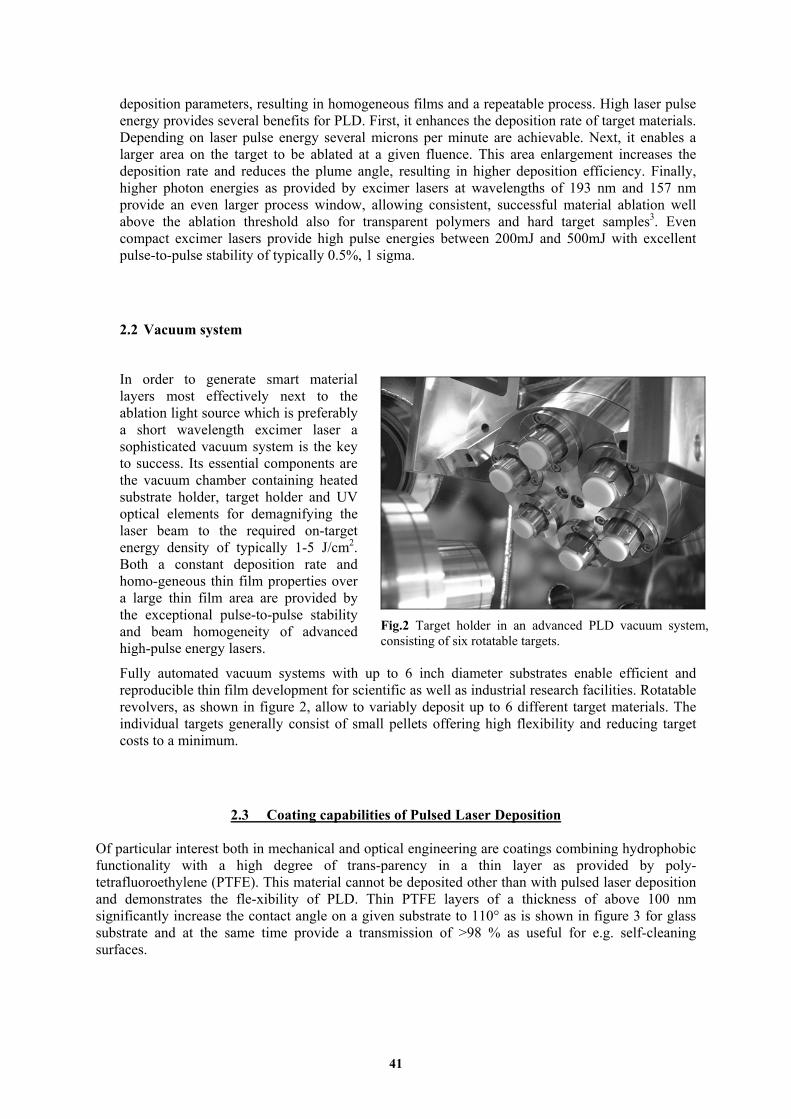
deposition parameters, resulting in homogeneous films and a repeatable process. High laser pulse energy provides several benefits for PLD. First, it enhances the deposition rate of target materials. Depending on laser pulse energy several microns per minute are achievable. Next, it enables a larger area on the target to be ablated at a given fluence. This area enlargement increases the deposition rate and reduces the plume angle, resulting in higher deposition efficiency. Finally, higher photon energies as provided by excimer lasers at wavelengths of 193 nm and 157 nm provide an even larger process window, allowing consistent, successful material ablation well above the ablation threshold also for transparent polymers and hard target samples3. Even compact excimer lasers provide high pulse energies between 200mJ and 500mJ with excellent pulse-to-pulse stability of typically 0.5%, 1 sigma.
2.2 Vacuum system
In order to generate smart material layers most effectively next to the ablation light source which is preferably a short wavelength excimer laser a sophisticated vacuum system is the key to success. Its essential components are the vacuum chamber containing heated substrate holder, target holder and UV optical elements for demagnifying the laser beam to the required on-target energy density of typically 1-5 J/cm2. Both a constant deposition rate and homo-geneous thin film properties over a large thin film area are provided by the exceptional pulse-to-pulse stability and beam homogeneity of advanced high-pulse energy lasers.
Fig.2 Target holder in an advanced PLD vacuum system, consisting of six rotatable targets.
Fully automated vacuum systems with up to 6 inch diameter substrates enable efficient and reproducible thin film development for scientific as well as industrial research facilities. Rotatable revolvers, as shown in figure 2, allow to variably deposit up to 6 different target materials. The individual targets generally consist of small pellets offering high flexibility and reducing target costs to a minimum.
2.3 Coating capabilities of Pulsed Laser Deposition Of particular interest both in mechanical and optical engineering are coatings combining hydrophobic functionality with a high degree of trans-parency in a thin layer as provided by poly-tetrafluoroethylene (PTFE). This material cannot be deposited other than with pulsed laser deposition and demonstrates the fle-xibility of PLD. Thin PTFE layers of a thickness of above 100 nm significantly increase the contact angle on a given substrate to 110° as is shown in figure 3 for glass substrate and at the same time provide a transmission of >98 % as useful for e.g. self-cleaning surfaces.
41
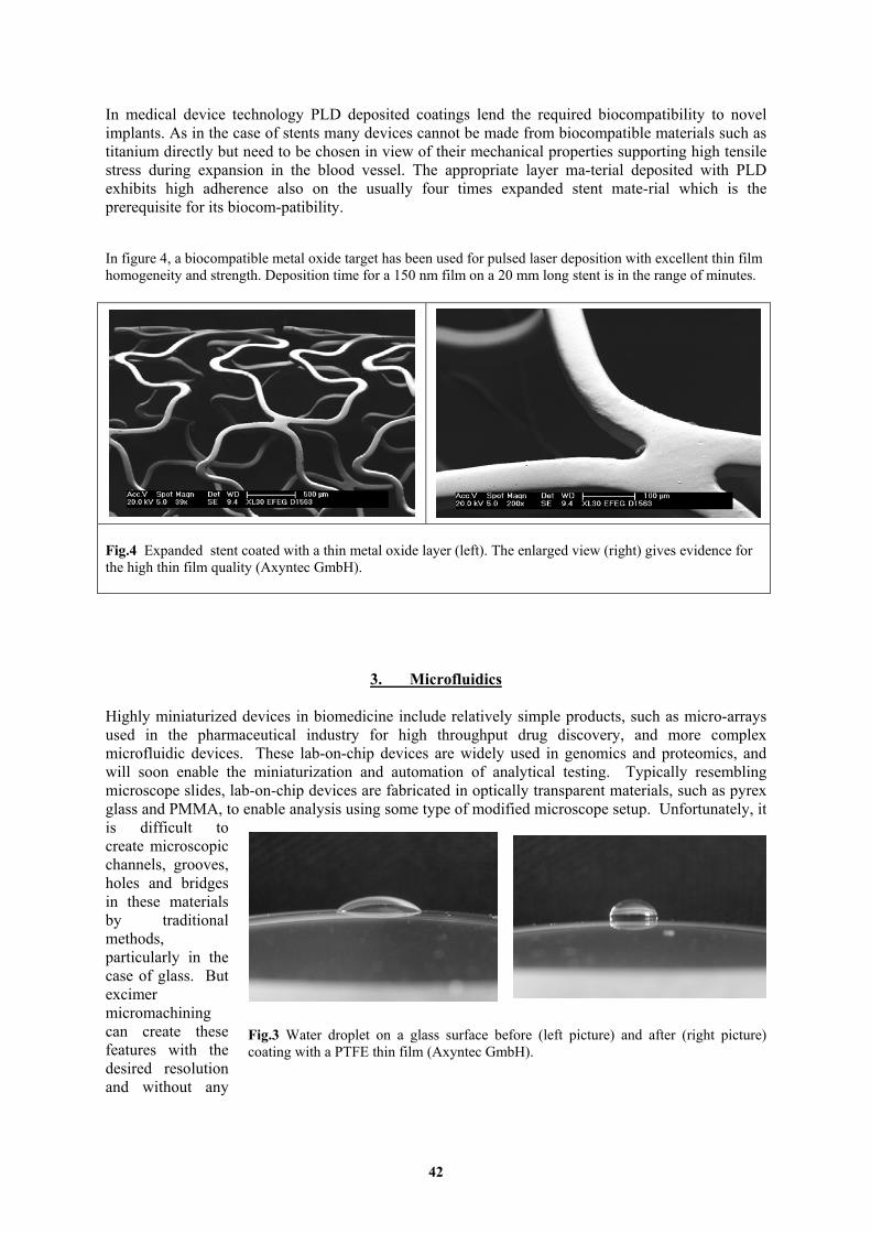
In medical device technology PLD deposited coatings lend the required biocompatibility to novel implants. As in the case of stents many devices cannot be made from biocompatible materials such as titanium directly but need to be chosen in view of their mechanical properties supporting high tensile stress during expansion in the blood vessel. The appropriate layer ma-terial deposited with PLD exhibits high adherence also on the usually four times expanded stent mate-rial which is the prerequisite for its biocom-patibility. In figure 4, a biocompatible metal oxide target has been used for pulsed laser deposition with excellent thin film homogeneity and strength. Deposition time for a 150 nm film on a 20 mm long stent is in the range of minutes.
Fig.4 Expanded stent coated with a thin metal oxide layer (left). The enlarged view (right) gives evidence for the high thin film quality (Axyntec GmbH).
3. Microfluidics Highly miniaturized devices in biomedicine include relatively simple products, such as micro-arrays used in the pharmaceutical industry for high throughput drug discovery, and more complex microfluidic devices. These lab-on-chip devices are widely used in genomics and proteomics, and will soon enable the miniaturization and automation of analytical testing. Typically resembling microscope slides, lab-on-chip devices are fabricated in optically transparent materials, such as pyrex glass and PMMA, to enable analysis using some type of modified microscope setup. Unfortunately, it is difficult to create microscopic channels, grooves, holes and bridges in these materials by traditional methods, particularly in the case of glass. But excimer micromachining can create these features with the desired resolution and without any
Fig.3 Water droplet on a glass surface before (left picture) and after (right picture) coating with a PTFE thin film (Axyntec GmbH).
42

microcracking or other problems (see figure). The 248 nm output wavelength is commonly used for polymers and the 193 nm wavelength is mostly used for glass and quartz machining. In addition, many lab-on-chip systems require electrical contacts, to enable processes such as electrophoresis. The excimer can also be used to fabricate these electrodes in the back-side of the lab-on-chip. Each electrode is produced by ablating a small through hole at the required location. These often have a circular cross-section with typical diameters of a few tens of microns or less. Other shapes can be created with an appropriate photomask, which also allows all the electrodes to be drilled in a single step. After laser-drilling, the holes are completely filled with metal in a vapor deposition or pulsed laser deposition process, forming both a liquid-tight seal and a through electrode (see fig. 5).
There is growing demand fodisposable medical sensors andfrom a 308 nm (XeCl) excime(typically chrome on quartz) cimaged at the work surface whbeen vapor-deposited. Most othe plastic-metal interface. Toverlying metal film (see figusingle laser pulse performs a c10 microns.
Fig.5 Microfluidic structure and sensors (Bartels Mikrotechnik, GmbH)
4. Direct Patterning of Circuits
r low unit cost, miniaturized electrical circuits for applications such radio frequency identifiers (RFID).In this application, the output beam r is reshaped in a beam homogenizer and passed through a photomask ontaining the pattern for one or even several circuits. The mask is re-ich consists of a plastic film or web on which a thin layer of metal has
f the UV radiation passes through the film and is strongly absorbed at his vaporizes a thin layer of the plastic, completely removing the re 6). Providing the metal layer thickness is 150 nanometers or less, a omplete lift with clean edges and no breaks even on lines as narrow as
43

The optimum thickness is actually around 500 angstroms which is more than sufficient for most flex circuit applications, which typically do not carry high current. At this thickness, a circuit with area up to 400 mm2 can be processed at a pulse energy of 1 J. Excimer lasers designed for this application typically operate at pulse repetition rates of several hundred Hz. At 300 Hz for example, this “single pulse” laser process can generate 18,000 circuits/minute. The pro-cess can be set up as reel-to-reel with continuous feed because the short pulse of the laser eliminates the possibility of blur even at feedrates of tens of meters/second. Alternatively some manufacturers have implemented a roll-to-roll process in which optics sweep across the web which undergoes stepped motion. Laser direct patterning can be used with several different flexible plastic substrates (PET, polyimide, PEN, and PMMA) and a full range of conductors including copper, gold, silver, platinum, aluminum, and even titanium. Manufacturers cite several process advantages, compared to traditional lithography using wet photochemistry. The most important is process simplicity; a single dry process replaces about seven separate steps. It also eliminates the cost and disposal of the chemical reagents. In addition, the metal debris can be trapped by a vacuum system, allowing recycling of this valuable material.
Fig.6 Laser Direct Patterning process (LPKF AG)
5. Conclusion Intelligent thin film development and rapid prototyping for various fields of applications is largely facilitated by means of short excimer laser wavelengths. Combined with compact, automated vacuum systems for fast and convenient substrate handling stoichiometric multi-layer thin-films with good homogeneity and taylored physical characteristics are efficiently generated. Stable, high pulse energy output characteristics provide controlled and reproducible target ablation for nanotechnology which can often be upscaled in output rate by reel to reel approaches.
6. References [1] Delmdahl, R F.; Oldershausen, G.:
Quantitative solid sample analysis by ArF excimer laser ablation, Journal of Molecular Structure, Vol. 744, p. 255-258 (2005).
[2] Ashfold, M. N. R.; Claeyssens, F.; Fuge, G. M.; Henley, S. J.: Pulsed laser ablation and deposition of thin films, Chemical Society Review, Vol. 33, p. 23-31 (2003).
[3] Pedarnig, J. D.; Peruzzi, M.; Vrejoiu, I.; Matei, D. G.; Dinescu, M.; Bäuerle, D.: Pulsed-laser deposition of inclined ZnO, of GaPO4 and of novel composite thin films, Applied Physics A, Vol. 81, p. 339-343 (2005).
44

IPT6 Precise photonic engines for UV pulsed laser deposition
R. Delmdahl, J. Sieber, B. Fechner
Coherent GmbH, Hans-Böckler-Str. 12, D-37079 Göttingen, Germany E-mail: [email protected]
Abstract
High pulse energy excimer lasers with pulse energies between 300 and 1200 mJ/pulse and photon energies between 5eV and 7.9 eV lend maximum flexibility to the technique of pulsed laser deposition. On account of the high energy densities accessible with the latest generation of excimer lasers, the entire material spectrum including high band-gap metal oxides such as ZnO is amenable to precise and controlled ablation with subsequent stoichiometric transfer to the substrat. Because the transferred material needs time to smoothly deposit and position itself optimally on the substrate, the repetition rate of the ablation laser is typically on the order of only 10 Hz. These requirements are best met by pulsed lasers with short wavelengths (248 nm is the most common), high pulse energies (100 to 1000 mJ) and homogeneous spatial energy distribution. Thin film quality is very sensitive to shot-to-shot energy density fluctuations, and because deposition time in a lab takes up to one hour, both spatial (beam profile) and temporal (shot-to-shot) energy stability are essential in order to obtain reproducible results.
1. Introduction Pulsed excimer lasers are the strongest and most efficient laser sources in the ultraviolet spectral region. Record short wavelengths from 351 nm down to 157 nm as well as record high 1200 mJ pulse energy as available for the 248 nm excimer lasers are commercially provided for numerous laser material ablation approachesi. Virtually no material is able to withstand the high photon energies ranging from 3.5 to 7.9 eV emitted by excimer lasers. As a result of the irradiation of material with high energy excimer laser photons at sufficient fluence immediate bond breaking due to electronic excitation is induced. In combination with short-term laser material interaction of only 10 to 30 ns excimer pulse duration, material ablation proceeds via fast vaporization and consecutive ejection of material with only negligible dissipation of heat transfer to the surrounding zone. The effect is an inherently precise and clean ablation quality. The latest excimer laser versions LPXPro and COMPexPro as described in this paper were specifically redesigned to provide the beam and energy stability required for achieving the homogeneous layer growth essential in todays’s most advanced thin film applications.
2. Advances in excimer laser tube design Excimer lasers used for precise material ablation must meet high standards in regards to performance and output characteristics. For reproducible results of high-quality the excimer laser must keep his performance stable over a long period in order to increase productivity even at very high pulse energies. In the following paragraphs recent technical advances in excimer lasers for pulsed laser deposition and resulting output energy characteristics and beam parameters are discussed.
2.1 Smooth Ceramic Preionization Based on proven metal-ceramic technology NovaTube®, the preionization concept of both the new LPXPro series and the new COMPexPro series has been optimized in order to obtain highest pulse
45
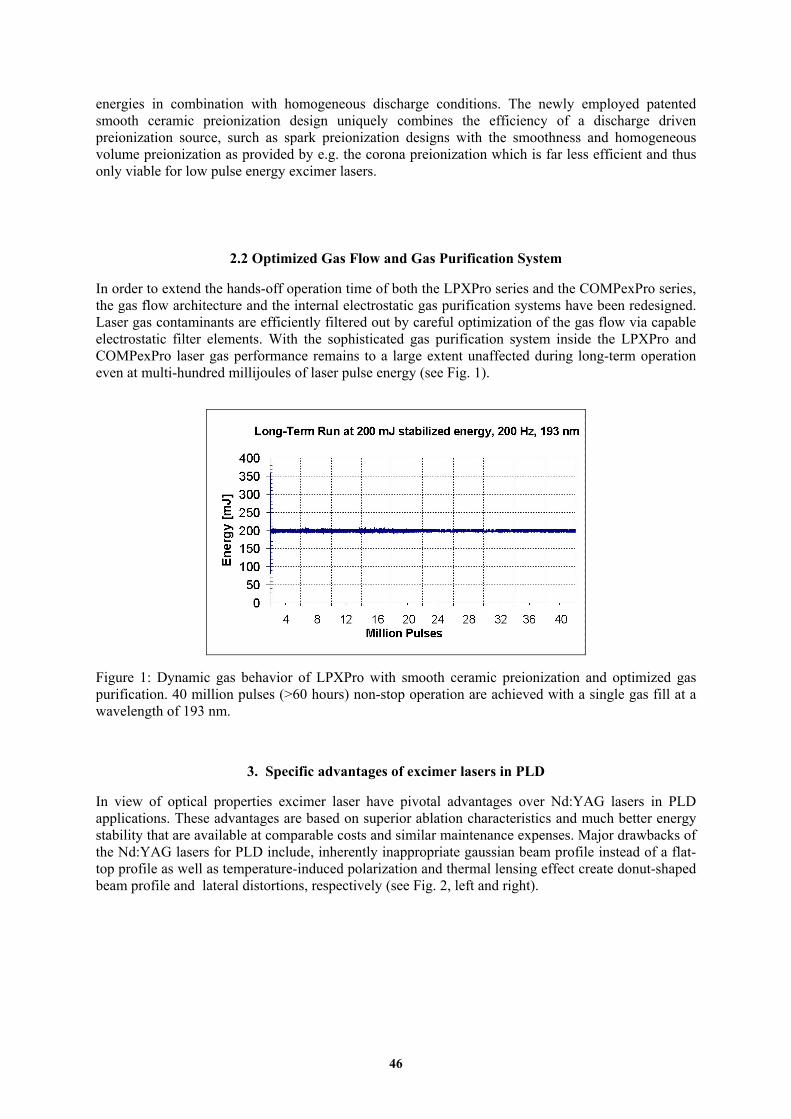
energies in combination with homogeneous discharge conditions. The newly employed patented smooth ceramic preionization design uniquely combines the efficiency of a discharge driven preionization source, surch as spark preionization designs with the smoothness and homogeneous volume preionization as provided by e.g. the corona preionization which is far less efficient and thus only viable for low pulse energy excimer lasers.
2.2 Optimized Gas Flow and Gas Purification System
In order to extend the hands-off operation time of both the LPXPro series and the COMPexPro series, the gas flow architecture and the internal electrostatic gas purification systems have been redesigned. Laser gas contaminants are efficiently filtered out by careful optimization of the gas flow via capable electrostatic filter elements. With the sophisticated gas purification system inside the LPXPro and COMPexPro laser gas performance remains to a large extent unaffected during long-term operation even at multi-hundred millijoules of laser pulse energy (see Fig. 1).
Figure 1: Dynamic gas behavior of LPXPro with smooth ceramic preionization and optimized gas purification. 40 million pulses (>60 hours) non-stop operation are achieved with a single gas fill at a wavelength of 193 nm.
3. Specific advantages of excimer lasers in PLD
In view of optical properties excimer laser have pivotal advantages over Nd:YAG lasers in PLD applications. These advantages are based on superior ablation characteristics and much better energy stability that are available at comparable costs and similar maintenance expenses. Major drawbacks of the Nd:YAG lasers for PLD include, inherently inappropriate gaussian beam profile instead of a flat-top profile as well as temperature-induced polarization and thermal lensing effect create donut-shaped beam profile and lateral distortions, respectively (see Fig. 2, left and right).
46

Fig. 2: Typical Nd:YAG laser beam profiles with rod polarization effects (left) and thermal lensing effect (right)
47
3.1 Wavelength and beam parameter considerations
the following section, the three key laser-related characteristics that are of particular relevance for
3.1.1 Laser-material interaction
) High-energy photons are directly absorbed by molecular bonds with lno bulk heating
Moreover, poor short-term and long-term pulse-to-pulse stability of typically 10 to 15%, rms are provided by Nd:YAG lasers due to the necessary frequency conversion the efficiency of which is severely degrading toward shorter output wavelengths such as 266 nm. Another limiting factor of Nd:YAG lasers in PLD experiments is the fixed repetition rate of 10 or 20 Hz which is not alterable but represents a fixed parameter. Table I gives an overview of excimer laser versus Nd:YAG with regard to photon energies, performance parameters, and maintenance. The overview clearly shows that excimer technology excels in photon energy, variability of use, long-term and short-term pulse stability, and ablation homogeneity.
Parameter Excimer Laser Photon Energy Flash-lamp pumped Nd:YAG Laser Wavelength
351nm, 308nm, 248nm 193nm 157nm
1.17eV 2.33eV 3.53eV 4.02eV 4.66eV 5.00eV 6.42eV 7.90eV
248nm: 100 to 1200mJ 193nm: 50 to 600mJ 157nm: 15 to 50mJ
variable, 1 to 200Hz 0.5 to 1%, rms 0 %, rms Flat-top profile
1064nm 532nm 355nm 266nm
Output Energy 355nm: 60 to 200mJ 266nm: 40 to 90mJ 213nm: 5 to 15mJ fixed, 10Hz (20Hz) 8 to 12%, rms 10 to 15%, rms “distorted Gaussian”
Repetition Rate Shot-to-Shot Stability Long Term Drift, 4hrs Ablation Geometry Pulse Width, FWHM 15 to 20ns 5 to 8ns Consumables Premix bottle, optics set Flash-lamps, crystals
InPLD experimenters are described in detail.
a

When a laser interacts with a solid surface, the laser energy is transformed into heat. The temp
48
Fig. 4: Nd:YAG ablation profile
erature f the solid material increases, leading to melting and evaporation of the solid material. Because the
stoichiometry and a smoother thin film without unwanted
) High photon energy results in better depth control and more controlled ablation conditions
. or excimer lasers at 193 nm and 248 nm, the ablation depth is in the 100 nm range. For 157 nm,
ue to shallow energy density gradients.
Fig. 3: Excimer laser ablation track in a PLD target.
) Shot-to-shot stability
solutely essential in PLD, because it determines the reproducibility of the in film material properties. Generally, excimer lasers exhibit a much better pulse-to-pulse stability
otemperature in the vapor plume can rise to high values (10,000K and higher), a plasma is formed. Besides atoms, electrons and ions, the material plume also consists of particulates, with dimensions ranging from nm to µm. The smallest particles (~nm size) are probably formed in the expanding vapor plume, by condensation of vapor atoms. The larger particles (~µm size) are probably created by direct ejection from the solid target. Moreover, at very high laser irradiance (above 1010 W/cm2), explosive boiling of the target material beneath the surface layer, as well as mass ejection of large particulates, may occur. Higher photon energies, or equally shorter wavelengths, yield faster plume heating and smaller particle sizes. The result is a preserved particulates. b The shorter the wavelength, the smaller the penetration depth of the laser radiation into the materialFpenetration depths are on the order of 50 nm. This limited penetration results in very controlled layer-by-layer ablation with virtually no volume heating, thus eliminating the ejection of particulates. Additionally, the laser energy is deposited in a very restricted volume, and the quick and even material evaporation leads to clean ablation zones. These are visible in figure 3, which shows a typical target ablation track cross section obtained with a 248 nm excimer laser. On the contrary, due to their rippled beam profile structure and longer wavelength, Nd:YAG laser beam ablation profiles (see Fig. 4) induce melting and uncontrolled material splashing dHigher photon energies or equivalent shorter wavelengths yield clean ablation zones.
c
Shot-to-shot stability is abththan frequency-converted Nd:YAG lasers (ref. Table I). As a matter of fact, COMPexPro lasers featuring ceramic preionization technology provide superior pulse-to-pulse stability of less than 1% rms at typical PLD conditions, i.e., at pulse energies of several hundred millijoules and repetition rates of typically 1 to 50 Hz. Note that even at 100 Hz operation, the energy stability is still 1% rms (see Fig. 5). This stable, high energy performance of the COMPexPro excimer series even at elevated repetition rates up to 100Hz is unprecedented. An integrated burst generator also enables bursts of pulses with precise energy, from the first to the last pulse of each burst.

350
F
AlIpada1
250
260
270
280
290
300
310
320
330
340
0 500 1000 1500 2000 250
Pulse Number
Pul
se E
nerg
y / m
J
COMPexPro burst over 25 seconds at 100 Hz, energy stabilizedAverage Energy= 298.91mJ, Std Dev.= 2.99mJ, Std.Dev.= 1%
ig. 5: Burst over 2500 pulses obtained with COMPexPro 110 at 248nm at a repetition rate of 100Hz.
3.1.2 Energy density and spot size
lack in pulse energy on first sight migh be compensated by tighter focusing. However, this leads to imitations in ablation and hence film quality. n fact, in PLD the excimer beam is not simply focused, as is shown in figure 6. Instead, the beam rofile is preferably imaged onto the target surface in order to achieve clean ablation conditions from flat-top, on-target energy distribution. Typically, the on-target image has a 1 to 5 mm2 area. This emagnification is easily obtained with the COMPexPro 100 series and 200 series, which also provide wide range of homogeneous on-target energy densities of 0.5J/cm2 to 15J/cm2, both at 248 nm and 93 nm wavelengths.
49

F W
F
dl
ol
Dd
sasr
fibaa
ig. 6: Excimer laser beam imaging versus focusing in Pulsed Laser Deposition.
hen the on-target laser spot size is decreas
1/u+1/v=1/f Demagnification= v/u
L
O
Image
u v
Focus
ed, the following problems occur: (1) the inhomogeneous n-target energy density distribution in the focal plane induces uncontrolled sub-surface boiling and
The smaller and maller spot sizes lead to an increasingly spherical plume geometry and a smaller fraction of material aches the substrate, which is typically located at a 3 to 5 cm distance from the target.
ig.7: Plume shapes obtained with small spot size (left) and larger spot size (right).
•
zers or ty is essential to achieve stoichiometric material transfer
om target to substrate. Only a homogeneous flat-top energy distribution of the excimer laser beam aged down to a homogeneous area of ca. 2mm2 onto the target can avoid uncontrolled sub-surface
oiling, splashing and material cracking, which otherwise results from energy density fluctuations
and the short axis has a gaussian like shape. The highly homogeneous spatial istribution of the COMPexPro beam profile obtained from a single shot exposure 70cm behind the aser exit at 400m is shown in
iquid m
3.1.3 Beam homogeneity
ue to direct imaging of the laser output beam on the target without the aid of homogeniiffractive optical elements spatial homogenei
aterial splashing; (2) large particulate ejection also occurs; (3) the deposition rate becomes maller and smaller as the spot size decreases, creating deposition times of an hour or longer; and (4) s the spot size decreases, the plasma plume becomes less directed (see fig. 9).
e
Laser Beam
rm
cross the ablation area. Excimer lasers have typically a rectangular beam profile, whereas the long xis has a top head
J pulse energy
50

Figure 8, The short axis cross-section g a near- n distribu e long ax t-top di e to the efficient and oth ceram ionization e in COM o and LP homogeneity tained at lse energy ion.
showin gaussia tion, th is the flastribution. Du smo ic pre schem PexPrXPro lasers this high is main high pu operat
Figure 8: Homogeneous beam profile of the COMPexPro excimer laser, with typical dimensions of 24 mm (FWHM, long axis) by 12 mm (FWHM, short axis). The short axis has a gaussian like distribution, whereas the long axis is flat top.
Table 2 summarizes the main specifications of the COMPexPro and LPXPro excimer lasers for wavelengths of 193 nm and 248nm.
COMPexPro LPXPro Wavelength 193 nm 248 nm 193 nm 248 nm Maximum pulse energy 400 mJ 700 mJ 650 mJ 1200 mJ Average power 12 W 30 W 50 W 90 W Maximum repetition rate 100 Hz 100Hz 200 Hz 200 Hz Energy stability (typical, sigma) < 2 % < 1 % < 2 % < 1 % Beam size (FWHM, v x h, typ.) 24 x 10 mm² 24 x 12 mm² 10 x 24 mm² 12 x 24 mm² Divergence (FWHM, v x h, typ.) 3 x 1 mrad² 3 x 1 mrad² 3 x 1 mrad² 3 x 1 mrad² Beam pointing stability (1 sigma) < 200 µrad < 50 µrad < 50 µrad < 200 µrad Pulse Length (typical, FWHM) 13 ns 20 ns 13 ns 20ns
• 4. Thin Film Applications
With proper focusing conditions the fluence of the excimer laser beam is sufficiently intense to vaporize any hard and transparent target material lending maximum flexibility in terms of the material spectrum which is to be ablated. On account of the unique lateral resolution of 2 µm achievable with short-wavelength excimer laser based ablation systems as well as of the high depth resolution
aching down to 0.1 µm, excimer lasers are extensively used in high-precision marking, surface treatment, micro patterning and microm but a few. Due to the unique spectral properties of excimer lasers, composites and allo enly ablated without fractionation of the
ed in reating thin films by means of the pulsed laser deposition technique (PLD). In this particularly
perpendicularly to the target surface in a highly irected so-called plasma plume consisting of excited and ionized species. The plume particulates
reachining to name
ys can be evdifferent constituents. Excimer lasers are hence the first-choice ablation sources to be employcstraightforward method a pulsed excimer laser beam focused on the target leads to rapid evaporation of the target material. The vaporized material recoilsd
51

evolve at high-speed toward the substrate which is typically located at some centimeters distance here they deposit and grow forming a thin film.
pulse repetition rate of the excimer laser need to be controlled during the process of thin film creation. The targets used in PLD are small compared with the large size required for other sputtering techniques. Multi-layered films of different materials are easily produced by sequential ablation of assorted targets on a rotating disk. By adapting the number of pulses, accurate control of film thickness down to atomic monolayer is possible. With the short wavelength excimer laser light the stoichiometry of the target like the crystal structure of the target can be retained. A recent overview over latest PLD developments is given in reference4.
• 5. Conclusion
The advanced high-pulse energy excimer laser series LPXPro and COMPexPro have been described in this paper. Based on proven technologies applied for industrial and lithography excimer laser sources, stable and cost-efficient, high-pulse energy lasers fitted to thin film production demands have been realized. The COMPexPro and LPXPro lasers deliver pulse energies up to 1200 mJ with high stability and beam homogeneity over many 10 million pulses hands-off operation at the preferred
ser wavelengths of 193 and 248 nm.
1 R. Delmdahl: LaserFocusWorld Supplement (2002) pp. 3. 2 T. Kuntze, M. Panzn al Symposium on Laser Precision Mic 3 G. Spiecker, R. Delmd
M. N. R. Ashfold, F. Claeyssens, G. M. Fuge, S. J. Henley: Chem. Soc. Rev., 33 (2003) pp. 23.
wThe PLD method is straightforward and only a few parameters including pressure, energy density and
la
• References
, July 2002, Optoelectronics World
er, U. Klotzbach, E. Beyer: Proc. 4th Internationrofabrication, Munich (2003) pp. 543.
ahl: Laser Magazin 6, (2002) pp. 10. 4
52

IPT7 Research and Development in Pulsed Laser Deposition:
A Scientometric Perspective
Ganesh Surwase, B.S. Kademani and Vijai Kumar Scientific Information Resource Division, Knowledge Management Group
Bhabha Atomic Research Centre, Mumbai-400 085 (India) E-mail: [email protected]; [email protected]
This paper attempts to highlight quantitatively the growth and development of world literature in the field of Pulsed Laser Deposition in terms of publication output as per Science Citation Index (1982-2006). During 1982-2006 a total of 8534 papers were published by the scientists in the field ‘Pulsed
aser Deposition’. The average number of publications published per year was 341.36. The highest
red ublications and 196 (2.30 %) single authored publications. Chinese Academy of Sciences (Peoples-
-Technol-Bomaby, umbai) with 38 publications, M.S. Hegde (Indian-Inst-Sci, Bangalore) with 31 publications, S.B.
Lnumber of papers 1074 were published in 2005. There were 84 countries involved in the research in this field. USA is the top producing country with 2014 publications (19.35%) followed by Japan with 1553 publications (14.92%), Peoples-R-China with 1106 publications (10.63%), Germany with 763 publications (7.33%) South Korea with 694 publications (6.67%) and France with 615 publications (5.91%). India ranked 9th among other countries with 291 publications during 1985-2006. Authorship and collaboration trend was towards multi-authored papers. There were 8338 (97.70%) multi-authopR-China) topped the list with 304 publications followed by Nanjing University (Peoples-R-China) with 244 publications, Tokyo Institute of Technology (Japan) with 233 publications and CNRS (France) with 217 publications. The most productive Indian institutions were: Tata Institute of Fundamental Research, Mumbai with 52 publications and Indian Institute of Science, Bangalore with 49 publications. The most prolific Indian authors were: R. Pinto (Indian-InstMOgale (Univ Poona, Poona) with 29 publications, L.M. Kukreja (Raja Ramanna Ctr-Adv-Technol, Indore) with 21 publications, P. Misra (Raja Ramanna Ctr-Adv-Technol, Indore) with 16 publications, R.K. Thareja (Indian-Inst-Technol-Kanpur) with 15 publications. The most preferred journals by the scientists were: Applied Physics Letters with 962 publications, Journal of Applied Physics with 714 publications, Applied Surface Science with 614 publications and Thin Solid Films with 541 publications. The high frequency keywords were: Pulsed Laser Deposition (3661), Thin Films (2611), Laser Ablation (1137), Films (571) and Silicon (562). Introduction
m ells of several sizes and shapes.
ulsed Laser Deposition as a film growth technique has gained importance and attracted wide spread
ed by the scientists, institutions and
Invention of laser in 1960 has opened up new areas of research and found various applications in many scientific fields. Pulsed Laser Deposition (PLD) is one of the several techniques of the deposition of the thin film on the substrates besides other techniques like Molecular Beam Epitaxy (MBE), Metal Organic Chemical Vapour Deposition (MOCVD) and Sputtering1-2. The Pulsed Laser Deposition has several advantages over other deposition techniques. There are several applications of the thin films developed because of its helpful technique in developing quantum dots and quantuw Pinterests after it has been used successfully to grow high-temperature Tc superconducting films3 in 1987. During the last decade, Pulsed Laser Deposition has been used to fabricate crystalline thin films with epitaxy quality. Ceramic oxide, nitride films, metallic multilayers, and various super-lattices grown by Pulsed Laser Deposition have been demonstrated. It has been reported in the literature that Pulsed Laser Deposition is being used to synthesise nanotubes4, nanopowders5 and quantum dots6. Evaluation is a key component of any research and development activity. One well known productivity indicator is the number of publications produc
53

countries. Studies like this will provide some insight into the complex dynamics of research acti ntists, policy makers and science administrators to provide adequate
cilities and proper guidance in which direction the research has to be conducted.
esearch publications are clearly one of the quantitative measures for the basic research activity in a
8-21.
Objectives
vity and enable the sciefa
Rcountry. It must be added, however, that what excites the common man, as well as the scientific community, are the peaks of scientific and technological achievement, not just the statistics on publications. There are also other kinds of research and technology development-mission oriented, industry-oriented, country-specific, etc., and progress in these cannot be obviously measured by counting only the number of publications7. Many scientometric studies have appeared in the literature to focus on the performance of science in various domains
The main objective of the study is to present the growth of world literature in Pulsed Laser Deposition and make the quantitative assessment of the research in terms of year-wise research output, geographical distribution of research output, nature of collaboration, characteristics of highly productive institutions, the characteristics of references cited in the publications and publications with more number of references in the field, the channels of communications used by the scientists, and the high frequency keywords appeared in the Key-Words-Plus and Author-Keywords field in the SCI. Materials and Methods Data was collected from the Science Citation Index-On Disc (CD-ROM) (1982-2006) published by a division of the Thomson Corporation (formerly Institute of Scientific Information, Philadelphia). Science Citation Index is one of the very comprehensive databases covering all aspects of science. The study period (1982-2006) is selected as the database is available in machine readable form since 1982. The search string ‘PULSED LASER DEPOSIT* OR PULSE LASER DEPOSIT*’ in the ‘BASIC INDEX’ field of SCI was used for the years 1982-2006 to download the records on the subject ‘Pulsed Laser Deposition’. A total of 8534 records were downloaded and analysed by using the spreadsheet application as per the objectives of the study.
Results a
igure that growth of the literature was ery low ed Laser epositio
nd Discussion
Growth of Publications in Pulsed Laser Deposition During 1982-2006 a total of 8534 publications were published in Pulsed Laser Deposition by various countries. The average number of publications produced per year were 341.36. The highest number of publications 1074 were produced in 2005. Figure–1 gives year-wise growth and collaboration rate in
ulsed Laser Deposition. It can be clearly visualized from the fPv during 1982-1990 and it peaked during 1991-2006. It indicates that research in Puls
n received a major impetus during this period. D
54

1982
1984
1986
1988
1990
1992
1994
1996
1998
2000
2002
2004
2006
0
100
200
300
400
500
600
Num
ber o
f Pu
Year
0
1000
2000
3000
4000
5000
Cum
ulat
ive
Num
ber o
700
800
900
1000
1100
1200
blic
atio
ns Number o f Publications
6000
7000
8000
9000
f Pub
licat
ions
Cumulative Number o f Publications
Figure-1: Year-wise publication productivity growth in PLD research
An exponential growth in number of publications was observed during 1982-2006. The highest growth rate (1154.55%) was found during 1987-1991 with 138 publications followed by (552.17%) with 900 publications during 1992-1996, (208.44%) with 2776 publications during 1997-2001 and (69.63%) with 4709 publications during 2002-2006. Table-1 gives the growth rate of publications in Pulsed Laser Deposition research in different five year blocks.
Table-1: Growth rate of publications in different five-year blocks in PLD research
Five Year Number of Growth Rate Blocks Publications (1982-2006)
1982-1986 11 - 1987-1991 138 1154.55 1992-1996 900 552.17 1997-2001 2776 208.44 2002-2006 4709 69.63
Geographical Distribution or Research Output There were as many as 84 countries carrying out research in the field of Pulsed Laser Deposition and
roduced 10409 authorships. Figure-2 provides a list of countries whose research output is more than 50 publications. USA is the g co 20 ions (19.35%), followed by Japan with 1553 publications Peop with 1106 publications (10.63%) Germany with 763 publications (7.33%), F ce with 615 ications ( ). Italy with 336 publications (3.49%), England with 297 publications (2.85%), India with 291 publications (2.80%) and Spain with 253 publications (2.43%).
p top producin
(14.92%), untry with
les-R-China 14 publicat
ran lpub 5.91%
55

USA
JAPA
N
PEO
PLES
-R-C
HINA
GER
MANY
SO
UTH-K
ORE
A
FRA
NC
E
ITALY
ENG
LAND
INDIA
SPA
IN
SIN
GAPO
RE
TAIW
AN
RO
MANIA
CANADA
RUS
SIA
SW
EDEN
NET
HERL
ANDS 0
200
400
600
800
1000
1200
1400
105
115
142
155
172
174
17525
3
291
297363
61569476
3
1106
Num
ber o
f pub
lic
Countries
1600
1800
2000
2200
1553
2014
ations
Figure-2: Country-wise distribution of number of publications (≥100) in PLD research (during the years 1982-2006 as per SCI database)
ab Pulsed Laser Deposition research. Out of 8534
Countries Publications Percentage
nternational Collaboration I
T le-2 gives the country-wise collaboration trend inpublications 1587 publications had international collaboration. Bilateral collaboration was found with 1335 (84.12%) publications and 205 (12.92%) publications had collaboration with three countries. Table-2: Country-wise collaboration trend in PLD research
Collaborating Number of
2 1335 84.12 3 205 12.92 4 38 2.39 5 8 0.50 6
00
ship and Collaboration Pattern
researcuth hip and collaboration tult thored publications. Only 196 (2.30bl tions (1622) accounted for 19.01 percent, follow authored 9) wi
7.80 ercent, three authorith .82 percent and seven aut percent.
1 0.06 Total 1587 100.
Author Authorship and collaboration trend in Pulsed Laser Deposition h is given in Figure-3. A ors rend was towards multi-authored papers. As there were 8338 (97.70%) m i-au %) were single-authored publications. Four authored pu ica ed by five publications (151 th 1 p ed publications (1268) with 14.86 percent, six authored publications (1179) w 13 hored publications (785) with 9.20
56

2 A
3 A
4 A
5 A
6 A
7 A
8 A
9 A
10 A
11 A
12 A
13 A
14 A
17 18 20 A
22 A
31 A
0 0
11252547
1519
8
1268
171
33
299
102
785
N u m b e r o f A u th o rs
1 A
15 16
A A A A
0
2 0 0
4 0 0
6 0 0
8 0 0
1 0 0 0
1 2 0 0
1 4 0 0
1 6
1 8 0 0
311 8
53
719
196
1622
1179
Num
ber o
f Pub
licat
ions
F re p and collaboration trend in PLD resea
rg In l, t organizations involved in the research in Pulsed Laser Deposition. Table-3 shows the organizations that have contributed 50 or more publications during 1982-2006. Chinese Academ -R-China) topped the list with 304 publications followed by Nanjing U ers titut apan) wi 33 p cat tifiq S) (France) with 217 p cat
T tutions as per number of publicat 0) in PLD research
l. No. Institute Country Publication
s
igu -3: Authorshi rch
O anisation-wise Distribution of Publications
al here were 2035
y of Science (Peoplesniv ity (Peoples-R-China) with 244 publications, Tokyo Ins
ions and Centre National De La Recerche Sciene of Technology (J th 2
ubli ue (CNRubli ions.
able-3: Distribution of insti ions (≥5
S1 CHINESE ACAD SCI PEOPLES-R-CHINA 304 2 NANJING UNIV PEOPLES-R-CHINA 244 3 TOKYO INST TECHNOL JAPAN 233
4 CENTRE NATIONAL DE LA RECERCHE SCIENTIFIQUE (CNRS) FRANCE 217
5 OSAKA UNIV JAPAN 196 6 UNIV TOKYO JAPAN 161 7 OAK RIDGE NATL LAB USA 158 8 CONSEJO SUPER INVEST CIENTIFICAS SPAIN 152 9 CONSIGLIO NAZIONALE DELLE RICERCHE (CNR) ITALY 148 10 UNIV MARYLAND USA 145 11 NATL UNIV SINGAPORE SINGAPORE 138 12 LOS ALAMOS NA 135 TL LAB USA 13 UNITED STATES NAVY USA 129 14 UNIV FLORIDA USA 124 15 INT SUPERCONDUCT TECHNOL CTR JAPAN 8 11
N CAR TATE UN 116HO ONG POL PEOPLES-R-CUN RIS FRANCE TO UNIV YO UNIV SOUTH-KOREA MA ANCK IN UCT PHYS GERMANY PEN ATE UNIV US
16 OLINA S IV USA 17 NG K YTECH UNIV HINA 114 18 IV PA 109 19 HOKU JAPAN 103 20 NSEI 101 21 X PL ST MICROSTR 97 22 N ST A 97
57

23 SEOUL N 91 ATL UNIV SOUTH-KOREA UNITED STATES AIR FORCE NATL INST ADV IND SCI & HNOL JAPAN NAT ST LAERS ADIAT PHYS ROMANIA NAG A UNIV NAT SING HU TAIWAN UNI IPZIG GERMANY NAT ST MAT S JAPAN ROY INST TE SWEDEN UNI MBRIDGE UNI LIF BERKEL USA ACA CI CZECHFUD UNIV PEOPLES-R-CHINA JAPKYO UNIV JAPAN KYU UNIV JAPAN ELE & TELECOMMUN INST SRUS N ACAD SCI INS STKORPER & W FFORSCH DRESDEN GERNAG A INST TECH JAPAN UNI ENTE NETPOH UNIV SCI & TEC SOUINR ERGIE & MAT CANADA QUE UNIV BELFAST NORTHINS TO NAZIONALE PER A FISICA DELLA MATERIA (INFTAT ST FUNDAMEN S INDIA UNI USTON USA UNI MA TOR V ITALY PUK G NATL U
Most Prolific Indian Authors There were 67 ndian ed 291 publications with 1423 authorships. Th c Indian (Indian-Inst-Technol-Bomab Mumbai) with 38 lica .S. Hegde (In ns, S.B. O le (Natl-Chem-L Poo blicatio Ramanna Ctr-Adv-Technol, I ore) with 21 publi ons, Raja Rama ions, R . Thareja (Indian-Inst-Tec pur) with 1 es the list of authors ho have contributed 5 or ications.
-4: Mo in PLD reseach (as
Sl. No. Num
Publications
3 authors in I publications who have publishe most prolifi authors were: R. Pinto y,
pub tions, M dian-Inst-Sci, Bangalore) with 31 publicatio gaab, na) with 29 pu ns, L.M. Kukreja (Raja ndcati P. Misra ( nna Ctr-Adv-Technol, Indore) with 16 publicat .K
hnol-Kan 5 publications. Table-4 provid wmore publ
Table st prolific Indian authors per SCI database 1982-2006)
Author Affialiation ber of
1 Pinto-R INDIAN-INST-TECHNOL-BOMABY, MUMBAI 38
24 USA 87 25 TEC 85 26 L IN PLASMA & R 81 27 OY JAPAN 80 28 L T A UNIV 80 29 V LE 80 30 L IN CI 79 31 AL CHNOL 79 32 V CA ENGLAND 77 33 V CA EY 76 34 D S REPUBL CZECH-REPUBLIC 75 35 AN 74 36 AN SCI & TECHNOL CORP JAPAN 74 37 TO 74 38 SHU 73 39 CTR RES OUTH-KOREA 72 40 SIA RUSSIA 71 41 T FE ERKSTO MANY 68 42 OY NOL 66 43 V TW HERLANDS 61 44 ANG HNOL TH-KOREA 56 45 S EN 55 46 ENS -IRELAND 54
47 TITU LM) ITALY 53
48 A IN TAL RE 52 49 V HO 51 50 V RO ERGATA 51 51 YON NIV SOUTH-KOREA 50
2 Hegde-MS INDIAN-INST-SCI, BANGALORE 31 3 Ogale-SB NATL-CHEM-LAB, POONA 29 4 Kukreja-LM RAJA RAMANNA CTR-ADV-TECHNOL, INDORE 21 5 Misra-P RAJA RAMANNA CTR-ADV-TECHNOL, INDORE 16 6 Thareja-RK INDIAN-INST-TECHNOL-KANPUR 15 7 Joseph-M INDIRA-GANDHI-CTR-ATOM-RES, KALPAKKAM 12 8 Kanetkar-SM UNIV POONA, POONA 12 9 Manoravi-P INDIRA-GANDHI-CTR-ATOM-RES, KALPAKKAM 12 10 Apte-PR TATA-INST-FUNDAMENTAL-RES, MUMBAI 11 11 Chaudhari-SM UNIV POONA, POONA 11 12 John-J TATA-INST-FUNDAMENTAL-RES, MUMBAI 10 13 Krupanidhi-SB INDIAN-INST-SCI, BANGALORE 10 14 Kumar-R CTR-NUCL-SCI, DIV MAT SCI, NEW-DELHI 10
58

15 Pai-SP TATA-INST-FUNDAMENTAL-RES, MUMBAI 10 16 Vispute-RD UNIV POONA, POONA 10 17 Hussain-OM SRI-VENKATESWARA-UNIV, TIRUPATI 9 18 Patil-SI UNIV POONA, POONA 9 19 Satyalakshmi-KM INDIAN-INST-SCI, BANGALORE 9 20 Adhi-KP UNIV POONA, POONA 8 21 Malik-SK TATA-INST-FUNDAMENTAL-RES, MUMBAI 8 22 Prasad-V INDIAN-INST-SCI, BANGALORE 8 23 Subramanyam-SV INDIAN-INST-SCI, BANGALORE 8 24 Godbole-VP UNIV POONA, POONA 7 25 Karunagaran-B BHARATHIAR-UNIV, COIMBATORE 7 26 Lekshmi-IC INDIAN-INST-SCI, BANGALORE 7 27 Mangalaraj-D BHARATHIAR-UNIV, COIMBATORE 7 28 Narayandass-SK BHARATHIAR-UNIV, COIMBATORE 7 29 Ramachandra Rao-MS INDIAN-INST-TECHNOL-MADRAS, CHENNAI 7 30 Ramamoorthy-K ALAGAPPA UNIVERSITY, KARAIKUDI 7 31 Sankaranarayanan-K ALAGAPPA UNIVERSITY, KARAIKUDI 7 32 Sharon-M BIRLA COLLEGE, KALYAN 7 33 Bhattacharya-P RAJA RAMANNA CTR-ADV-TECHNOL, INDORE 6 34 Budhani-RC INDIAN-INST-TECHNOL-KANPUR, KANPUR 6 35 Gupta-LC TATA-INST-FUNDAMENTAL-RES, MUMBAI 6 36 Gupta-V UNIV DELHI, DELHI 6 37 Koinkar-VN UNIV POONA, OONA 6 P
-U38 Kumar-RTR BHARATHIAR NIV, COIMBATORE 6 39 Ramana-CV SRI-VENKATESWARA-UNIV, TIRUPATI 6 40 Raychaudhuri-P TATA-INST-FUNDAMENTAL-RES, MUMBAI 6 41 Vasanthacharya-NY INDIAN-INST-SCI, BANGALORE 6 42 Venimadhav-A INDIAN-INST-SCI, BANGALORE 6 43 Venkatesan-T UNIV POONA, POONA 6 44 Vitta-S INDIAN-INST-TECHNOL-BOMABY, MUMBAI 6 45 Choudhary-RJ UNIV POONA, POONA 5 46 Date-SK UNIV POONA, POONA 5 47 Ganguli-T RAJA RAMANNA CTR-ADV-TECHNOL, INDORE 5 48 Gayen-A INDIAN-INST-SCI, BANGALORE 5 49 James-AR SOLID-STATE-PHYS-LAB, DELHI 5 50 Jayachandran-M CENT-ELECTROCHEM-RES-INST, KARAIKKUDI 5 51 K 5 shirsagar-ST NATL-CHEM-LAB, PUNE
undaliya-DC TATA-INST-FUNDAMENTAL-RES, MUMBAI 52 K 5 53 Manoharan-SS INDIAN-INST-SCI, BANGALORE 5 54 h-C SOLID-STATE-PHYS-LAB, DELHI 5 Prakas
Pur re-SC TATA-INST-FUNDAMENTALSan raja-C ALAGAPPA UNIV
ibu n of Indian Contribution in Pulsed Laser De
bu of Indian contribution in the fwe 91 publications published during ly ocati were published during 198
ears 2003 and 2005 respectively. The average num
55 anda -RES, MUMBAI 5 56 jeevi ERSITY, KARAIKUDI 5
Year-wise Distr tio position Year-wise distri tion ield of Pulsed Laser Deposition is given in Figure-4. There re 2 1985-2006. There was on ne publication in 1985. No publi ons 6-1987. The highest number of publications (41) were published in the y ber of publications per year was 13.22.
59

1986
1990
1992
1994
1996
1998
2000
2004
2006
0
5
1 0
1 5
2 0
4 5
N u m b e r o f P u b lic a t io n s
Nu
r of
s
Y e a
0
5 0
1 0 0
1 5 0
2 5 0
3 0 0
Cum
ulat
ive
mbe
r otio
nss
4 0 C u m u la t iv e N u m b e r o f P u b lic a t io n
2 5
3 0
3 5
Pub
licat
ion
2 0 0
f Pub
lica
mbe Nu
1988
2002
r
ndian ions
Figure-4: Year-wise distribution of I publicat in PLD research
Sl. No. Institute Publications
Distribution of Indian Institutions in Pulsed Laser Deposition There were 73 research institutes and universities involved in research in pulsed laser deposition. The leading institutes were Tata Institute of Fundamental Research, Mumbai with 52 publications, Indian Institute of Science, Bangalore with 49 publications, University of Poona, Poona with 38 publications, Indian Institute of Technology, Kanpur with 28 publications, Raja Ramanna Centre for Advanced Technology, Indore with 24 publications and Indira Gandhi Centre for Atomic Research, Kalpakkam with 18 publications. Table-5 provides a list of prominent Indian research institutes which had published five or more publications.
Table-5: Distribution of Indian Research Institutes in PLD research
1 52 TATA INST FUNDAMENTAL RES, MUMBAI 2 INDIAN INST SCI, BANGALORE 49 3 UNIV POO NA 38 NA, POO
5 RAJA RAMANNA CTR ADV TECHNOL, INDORE 24 6 INDIRA GANDHI CTR ATOM RES, KALPAKKAM 18 7 CTR NUCL SCI, NEW DELHI 13 8 INDIAN INST TECHNOL BOMBAY 13 9 INDIAN INST TECHNOL MADRAS 10
10 IUC DAE FACIL, INDORE 10 11 NATL CHEM LAB, POONA 10 12 SRI VENKATESWARA UNIV, TIRUPATI 10 13 UNIV DELHI, DELHI 10 14 BHABHA ATOM RES CTR, MUMBAI 9 15 SOLID STATE PHYS LAB, NEW DELHI 9 16 ALAGAPPA UNIV, KARAIKKUDI 8 17 BHARATHIAR UNIV, COIMBATORE 7 18 COCHIN UNIV SCI & TECHNOL, COCHIN 7 19 SAURASHTRA UNIV, RAJKOT 7 20 UNIV HYDERABAD, HYDERABAD 7 21 NATL PHYS LAB, NEW DELHI 6 22 CENT ELECTROCHEM RES INST, KARAIKKUDI 5 23 INDIAN ASSOC CULTIVAT SCI, KOLKATA 5
4 INDIAN INST TECHNOL KANPUR 28
60

Prefe mmunication by Scientists
Scien communications channels. Table-6 ic at 97.25 percent of the literature was published in journal by eviews 1.34 ce ercent.
ublications in various channe ti
Document Type Publications Percentage
rence of Channels of Co
tists communicated their publications through variety of ts thdep articles followed r
per nt, notes 0.46 percent and letters 0.42 p
Table-6: Distribution of p ls of communica on
Articles 8299 97.25 Reviews 114 1.34 Notes 39 0.46 Letters 36 0.42 Meeting-Abstracts 27 0.32 Corrections 11 0.13 Editorial-Materials 4 0.05 News-Items 4 0.05 Total 8534 100
Preference of Journals for Communication by Scientists The distribution of publications were spread over 315 journals. The leading journals preferred by the scientists were Applied Physics Letters with 962 publications followed by Journal of Applied Physics with 714 publications, Applied Surface Science with 614 publications, Thin Solid Films with 541 publications, Physica C with 432 publications, Applied Physics- A with 320 publications and Japanese Journal of Applied Physics-I with 269 publications. Table-7 provides journal-wise scattering of publications. More than 92 percent of the publications were published in the journals with impact factors ranging from 0.01 to 32.18. This indicates that the publication behaviour of scientists who prefe the publ per
-5.
Sl s
rred to publish their publications in high impact-factor journals. About 22.43 percent of ications were published in the journals having no impact-factor. The distribution of journals as
impact factors range is given in the Figure
Table-7: Journals publishing articles (≥50) in PLD research
. No. Journal Country IF-2005 Publication
1 APPLIED PHYSICS LETTERS USA 4.127 962 2 JOURNAL OF APPLIED PHYSICS USA 2.498 714 3 APPLIED SURFACE SCIENCE NETHERLANDS 1.263 614 4 THIN SOLID FILMS SWITZERLAND 1.569 541 5 PHY 432 SICA -C NETHERLANDS 0.948
LIED PHYSICS -A USA 1.990 6 APP 320 7 JAPANESE JOURNAL OF APPLIED PHYSICS -I JAPAN - 269 8 PHYSICA 85 196 L REVIEW- B USA 3.1
RYSTAL NETHE ANDS 1.6CTIVITY USA
ONDUCTOR ENGATED FERROELE ENG
H USAL OF VACU - A USAE & COAT SW D
SW D SO A SW D
SE JOURNAL OF YS JAPL OF MAGNE GN NE DS
9 JOURNAL OF C GROWTH RL 81 193 10 IEEE TRANSACTIONS ON APPLIED SUPERCONDU 1.071 177 11 SUPERC SCIENCE & TECHNOLOGY LAND 1.896 177 12 INTEGR CTRICS LAND 0.345 161 13 JOURNAL OF MATERIALS RESEARC 2.104 155 14 JOURNA UM SCIENCE & TECHNOLOGY 1.399 137 15 SURFAC INGS TECHNOLOGY ITZERLAN 1.646 135 16 MATERIALS SCIENCE AND ENGINEERING- B ITZERLAN - 127 17 JOURNAL OF THE KOREAN PHYSICAL SOCIETY UTH KORE 0.828 122 18 DIAMOND AND RELATED MATERIALS ITZERLAN 1.988 113 19 JAPANE APPLIED PH ICS - II AN - 112 20 JOURNA TISM AND MA ETIC MATERIALS THERLAN 0.985 104
61

21 FERROELECTRICS ENTATE C ENL OF PHY EN
IALS LETTL OF PHYSICS-CO M EN
S RES NE DS
USUSSWI D
GLAND 0.459 96 22 SOLID S OMMUNICATIONS GLAND 1.489 94 23 JOURNA SICS- D GLAND 1.957 90 24 MATER ERS NETHERLANDS 1.299 67 25 JOURNA NDENSED ATTER GLAND 2.145 64
26 NUCLEAR INSTRUMENTS & METHODS IN PHYSIC EARCH - B THERLAN - 56
27 IEEE TRANSACTIONS ON MAGNETICS A 1.014 53 28 JOURNAL OF THE ELECTROCHEMICAL SOCIETY A 2.190 53 29 MATERIALS SCIENCE FORUM TZERLAN 0.399 52
0.
00-0
.00 0
1.01
-1.5
0
1.51
-2.0
0
2.51
-3.0
0
3.01
-3.5
0
4.01
-4.5
0
4.51
-5.0
0
5.01
-10.
00
10.0
1-20
.00
20.0
1-30
.93
0
2 5 0
5 0 0
7 5 0
1 0 0 0
Num
ber o
f pub
l
Im F a c to r r
2 0 0 0
1 2 5 0
1 5 0 0
1 7 5 0
catio
ns
0.00
-
0.51
0.5
-1.0
0
2.01
-2.5
0
3.51
-4.0
0
p a c t- a n g e
Figure-5: Impact-factor range and distribution of journals publishing articles in PLD research
ountry-wise Distribution of Journals
sed Laser Deposition research were spread over 20 ountries. Table-8 gives country-wise distribution of journals and publications. USA has published
country
Number of journals Percentage Number of
publications Percentage
C The Journals (315) publishing articles in Pulc3300 (38.67%) publications in 102 (31.29%) journals, publications followed by England with 1257 (14.73%) publications in 83 (25.46%) journals, Netherlands with 1854 (21.72%) publications in 46 (14.11%) journals, Switzerland with 1176 (13.78%) publications in 22 (6.75%) journals and Germany with 129 (1.51%) publications in 21 (6.44%).
Table-8: Country-wise distribution of journals publishing articles in PLD research
Journal publishing
USA 102 31.29 3300 38.67 ENGLAND 14.73 83 25.46 1257
46 14.11 1854 NETHERLANDS 21.72 SWITZERLAND 22 6.75 1176 13.78 GERMANY 6.421 4 129 1.51 FRANCE 10 3.0 0.75 7 64
10 PEOPLES R CHINA 2.7 0.60 9 6 51
4 3 64 3 131
SINGAPORE 3 0.92 76 0.89
JAPAN 3.07 427 5.00
RUSSIA 1.2 0.07 SOUTH KOREA 1.2 1.54
62

AUSTRIA 2 0.6 0.05 1 4 INDIA 2 0.6 0.11 1 9 POLAND 2 0.61 13 0.15 CANADA 0.3 0.01 1 1 1
1 ITALY 1 0.3 4 0.05 1
1 1 1 1 1
TAIWAN 0.3 0.09 1 1 8 Total
utio ations in Pulsed sh whe most predominant langua 8468 publications, follow0.42%) publica (0.1 ch 184 0.430%) publ0.07%) publ (0.0 ations.
age- ution of publications
Per990.42
0.11 0.07
CZECHREPUBLIC 0.31 17 0.20
MEXICO 0.3 6 0.07 ROMANIA 0.3 0.01
326 100 8534 100 Language-wise Distribution of Publications Table-9 depicts the language-wise distrib n of public Laser Deposition. Engli as t ge with (99.23%) ed by Chinese with 36 ( tions, Japanese with 14 6%), Fren ications, Russian with 9 ( ications and Spanish with 1 1%) public
Table-9: Langu wise distrib
Language Publications centage English 8468 .23 Chinese 36 Japanese 14 0.16 French 9 Russian 6 Spanish 1 0.01 Total 8534 100
Distribution of Keywords Keywords are one of the best scientometric indicators to understand and grasp instantaneously the thought content of the papers and to find out the growth of the subject field. By analyzing the keywords appeared either in the title or assigned by the indexer or the author himself help in knowing in which direction the knowledge grows. The high frequency keywords will enable us to understand what are all the aspects that have been studied. In the current study the keywords appeared in the Key-Words-Plus field and Author Keywords in SCI were analysed for the purpose. The high frequency keywords were: Table-10 lists the keywords appeared 100 or more times in the Key Word Plus field and Author Keywords in SCI.
Table-10: Keywords with ≥ 100 frequencies appeared in Key-Word-Plus field and Author-Keywords in SCI in PLD research
Keyword Frequency
PULSED LASER DEPOSITION 3661 THIN FILMS 2611 OXIDES 373 LASER ABLATION 1137 FILMS 571 SILICON 562
ZINC OXIDE 367 OPTICAL PROPERTIES 361
DEPOSITION 478
CHEMICAL VAPOR DEPOSITION 436 TEMPERATURE 391
LAYERS 303
EPITAXIAL GROWTH 367
63

ELECTRICAL PROPERTIES 286 RUCTURE 277 LAR BEAM EPITAXY 271
LUMINESCENCE 139 MAGNETIC PROPERTIES 138 CRYSTALS 135
MICROSTMOLECUBUFFER LAYERS 263 SAPPHIRE 252
ORESISTANCE 243
TRANSITION 134 CERAMICS 133 FATIGUE MAGNET
SURFACE 225 219 ORS
INTERFACE 132 PEROVSKITES 130
133
EPITAXYCAPACIT 215 X RAY DIFFRACTION 210 DIELECTRIC PROPERTIES 200
MINESCENCE 195 D LIKE CARBON
FERROELECTRIC THIN FILMS 123 AMORPHOUS CARBON 122 MEMORIES 122
SINGLE CRYSTALS 126
PHOTOLUDIAMON 186 EVAPORATION 183
MPERATURE GIANT MAGNETORESISTANCE 119 SUPERCONDUCTIVITY 122
ROOM TE 179 SUBSTRATE 179
CURRENT DENSITY 172 MULTILAYERS 116 SEMICON
EMISSION 116
CRITICALFABRICATION 171 BEHAVIOR 170
TRUCTURES 170 S 162
GRAPHITE 114 RESISTIVITY 111 OXYGEN 107 FERROELECTRIC PROPE
DUCTORS 116
HETEROSCOATINGSPECTROSCOPY 158
156 PLASMA 106 COATED CONDUCTORS 105
RTIES 106
MGO SRTIO3 154 DEPENDENCE 153 DEVICES 153
O7 DELTA 150
PHASE 104 STRAIN 104 LASER DE
ORIENTATION 105
YBA2CU3ELECTRODES 149
TTICES 146 GAN 102 TRANSPORT 101
POSITION 103
SUPERLASUPERCONDUCTORS 143
142 MANGANITES 100
SYSTEM
Conclusi
on
comes newhich magrowth of publications was observed which indicates the sustained impetus received for the research
g 19more thatremendo oration trend is towards multi-
publicatioInstitute 3 publications and CNRS (France) with 217 publications.
Indian in d
were pubof scienti uted journals. Citation analysis of these
rs ma Referenc
2. thin films, John-Wily, (1994).
USA is the major producer of scientific output with 2014 publications to its credit in this field. Japan xt with 1553 publications. The growth of the literature was very low during 1982-1990 y be attributed for not receiving boost for research in this field. Since 1991, an exponential
durin 91-2006. Four countries (USA, Japan, Peoples-R-China and Germany) have contributed n fifty percent of the total publications indicates that these countries have received us official support for the research in this field. Collab
authored papers. Chinese Academy of Sciences (Peoples-R-China) topped the list with 304 ns followed by Nanjing University (Peoples-R-China) with 244 publications, Tokyo
of Technology (Japan) with 23India ranked 9th among other countries with 291 publications during 1985-2006. The most productive
stitutions were: Tata Institute of Fundamental Research, Mumbai with 52 publications anIndian Institute of Science, Bangalore with 49 publications. More than 92 percent of the publications
lished in the journals with impact factors which is suggestive of the publications behaviour sts who preferred to publish their papers in highly rep
pape y give interesting insights into the dynamics of this field.
es:
1. D.J. GARDINER, P.R. GRAVES, Practical pulsed laser deposition, Springer-Verlag, (1989). D.B. CHRISEY, G.K. HUBLER, Pulsed laser deposition of
64

3. D. DIJKKAMP, T. VENKATESAN, X.D. WU, S.A. SHAHEEN, N. JISRAWI, Y.H. MIN-LEE, W.L. McLEAL, M. CROFT, Preparation of Y-Ba-Cu oxide superconductor thin films u
4. Y. ZHANG, H. GU, S. LI tubes synthesized by laser ablation in a nitrogen atmosphere, A (1998). 3827-3829.
. n 4
6. is
7. 8
8. J. LAWSON, B. KO etric study on a new subject: Energy analysis, Scie
ogram: the case of the European ‘non-nuclear’ energy program, Scientometrics, 22 (1)
14. es of indicators and their trics, 24 (2) (1992) 237-
5. KUMAR, Scientometric based on INIS
on Science, 11 (1) (2006)
16. MAR, LALIT MOHAN, earch in India, DESIDOC
17. AI KUMAR, Mapping of Library and Information
18. KUMAR, World literature on 69 (2) (2006) 347-364.
19. tical Chemistry in nuclear analytical chemistry in
MOHAN, Electrochemistry research ia: A scientometric view. In: International conference on Electroanalytical Chemistry and Allied Topics (ELAC-2007), March 10-15, 2007, 1-21.
21. ANIL SAGAR, B.S. KADEMANI, VIJAI KUMAR, Scientometric mapping of mass spectrometry research in nuclear science and technology. In: ISMAS symposium cum workshop on mass spectrometry, March 25-30, 2007, 1-16.
sing pulsed laser from high Tc bulk material, Applied physics letters, 51 () (1998) 619-621. JIMA, Single-wall carbon nano
pplied physics letters, 73 (26)5 D.B. GEOHEGAN, A.A. PURETZKY, D.J. READER, Gas-phase nanoparticle formatio
and transport during pulsed laser deposition of Y1Ba2Cu3O7-d, Applied physics letters, 7(25) (1999) 3788-3790. T.J. GOODWIN, V.J. LEPPERT, S.H. RISBUD, I.M. KENNEDY, H.WH. LEE, Synthesof gallium nitride quantum dots through reactive laser ablation, Applied physics letters, 70(23) (1997) 3122-3124. R. CHIDAMBARAM, Measures of progress in science and technology, Current Science, 8(6) (2005) 856-860.
STREWISKI, C. OPPENHEIM, A bibliomntometrics, 2 (3) (1980) 227-237.
9. R.K. VERMA, Y.K. SHARMA, H.S.D. KHATRI, Trends in nuclear research and its publications: An analysis based on five years coverage in the Indian Science Abstracts, Annals of Library Science and Documentation, 29 (2) (1982) 64-69.
10. D.H. HALL, The interface between geoscience and industry: A case study of the interaction between research and discovery and mining of areas for nuclear fuels, Scientometrics, 11 (3-4) (1987) 199-216.
11. P. TROFIMENKO, Scientometric analysis of the development of nuclear physics during the last 50 years, Scientometrics, 11 (3-4) (1987) 231-250.
12. H. J. CZERWON, Scientometric indicators for a specialty in theoretical high energy physics: Monte Carlo methods in lattice field theory, Scientometrics, 18 (1-2) (1990) 5-20.
13. P. MAVGUIN, Using a contracts database for evaluating the dynamics of a technological pr(1991) 207-228. D.H. HALL, The Science-industry interface: Correlation time serispectra, and growth models in the nuclear fields industry, Scientome280. B.S. KADEMANI, VIJAI KUMAR, ANIL SAGAR, ANILdimensions of nuclear science and technology research in India: A study(1970-2002) database, Malaysian Journal of Library and Informati23-48. B.S. KADEMANI, VIJAI KUMAR, ANIL SAGAR, ANIL KUGANESH SURWASE, scientometric dimensions of thorium resBulletin of Information Technology, 11 (2) (2006) 87-104. B.S. KADEMANI, GANESH SURWASE, ANIL SAGAR, VIJliterature on Bose-Einstein Condensation. Malaysian Journal ofScience, 11 (2) (2006) 87-104. B.S. KADEMANI, VIJAI KUMAR, ANIL SAGAR, ANILthorium: A study based on Science Citation Index, Scientometrics, B.S. KADEMANI, ANIL KUMAR, VIJAI KUMAR, Analyscience and technology. In: DAE-BRNS symposium on role of nuclear technology, January 4-6, 2007, 135-148.
1
20. ANIL KUMAR, B.S. KADEMANI, VIJAI KUMAR, GANESH SURWASE, LALIT in Ind
65

OPT1
Large Room Temperature Magnetization of Pulsed Laser Deposited Cobalt Ferrite Thin Film
Subasa C. Sahoo1, M. Bo ra1 and R. Krishnan3
1Department of physics,In i, Mumbai – 400076, 2Department of Metallurgical Engineering and Material Science, Indian Institute of Technology
Bombay Powai, Mumbai – 400076,3Groupe d'étude de la matière condensée, CNRS / Universite de
*
Pulsvariferr(Filhoushofouthinwerundpro
hra1, N.Venkataramani2#, Shiva Prasad1*, D. S. Mis
dian Institute of Technology Bombay Powa
Versailles-St-Quentin, 45, avenue des Etats-Unis, 78035 Versailles Cedex, France Current Address: Director, Indo-French Centre for Promotion of Advanced Research, 5B, India
Habitat Centre, New Delhi-110003 # Corresponding Author; [email protected]
ed laser deposition technique is a very convenient and successful method for the growth of a ety of thin films. We have deposited cobalt ferrite thin films using this technique from cobalt ite target. In this work, two films, one deposited at insitu substrate temperature (TS) of 750 ºC m-1) and another deposited at ambient temperature and exsitu annealed at 750 ºC in air for two rs (Film-2) were studied. Single phase cobalt ferrite was observed by XRD in both the films. Fig.1 ws MH loops of both the films and that of the target used. The 4πMS value of the Film-1 was nd to be 3490G which is less than that value of 5360G of the target, which is generally expected in films. But in the Film-2 the 4πMS value was found to be 5820G. Coercivity and MR/MS ratio e found to be 1.76kOe, 0.33 and 0.86kOe, 0.37 for Film-1 and Film-2 respectively. It was erstood that insitu heating and external annealing affect the microstructure and hence the magnetic perties.
-6
-4
-2
0
2
4
6
8
Target
Film-2
-2000-1500-1000 -500 0 500 1000 1500 2000-2500-2000-1500-1000-500
0500
1000150020002500
4πM
( G
)
H ( Oe )
4πM
( K
G )
Film-1
H ( T )
Fig. y of the films and the
-8 -6 -4 -2 0 2 4 6 8-8
1 MH loops of both the films and of target used. Inserted fig. shows coercivit
target.
66

OPT2
Photoluminescence of ZnO nanowires grown by thermal evaporation on pulsed laser deposited Zn
A. Mohanta, A. P. Singh, andna S., and R. K. Thareja Department of Physics an Centre for Laser Technology,
Ind 08016
ZnO is a semi-conduct both microelectronics and optoelectronics. Due to i mperature) and direct wide band gap (3.37 eV), it has been a promising cand e for efficient ultraviolet emitters as high excitonic binding energy gives assurance of excitonic recombination at room temperature1. The synthesis of 1D nanostructures such as nanowires, nanorods etc. has become a great interest due to the size effect and
properties is rarely reported. In this article, we demonstrate a simple approach to synthesize nanowires on Si substrate coated with pulsed laser deposited ZnO thin films. Photoluminescence study is also undertaken. A thin buffer layer of ZnO film eposited on silicon substrates by PLD system. The target was a ZnO pellet (99.99%) which is sintered at 1000oC for five hours. The silicon substrate was kept at 4 cm distance parallel to the target surface at 515 . The third harmonics of Nd: YAG laser beam (DCR-4G, Spectra Physics, ν = 10 Hz, FWHM = 5 ns) w focused through a lens onto a rotating target at a 45o angle of incidence. The deposition chamber was in ially evacuated down to a pressure of 6.8 x 10⁻⁷ mbar, and then oxygen gas was introduced into the chamber to maintain oxygen pressure of 1.2 x 10⁻² mbar. After film deposition, nanostructures of ZnO were fabricated by using a simple thermal evaporation process. A mixture of ZnO powders and carbon with molar ratio 1:1 were used as source materials. The source materials were kept at 950o C for 30 minutes and the ZnO coated Si substrate was kept at 19.8 cm from the source position. The whole system was held at a b ressure of 3 x 10⁻² Torr under the constant flow of argon with a flow rate of 40 sccm. Figure-1 show e SEM images of ZnO nanowires deposited on ZnO coated Si substrates. It is obvious that the wires are nding to form closed loop and one such loop is shown in figure-1 (b). The diameters of the wires distrib e in the range of 101 – 125 nm and have an average value of 113 nm. Figure-2 shows photoluminescence profile of the nanowires at room temperature. The UV emission band at 380 nm is due to a near-ban -edge (NBE) transition which is the recombination of free excitons through exciton-exciton collision pro ess, 4 as shown in figure-2(a). Figure – 2(b) shows a deep-level emission band which falls in the visible region. There are many suggested sources of deep-level emission.5In this case; they are expected to be due to oxygen related defects such as oxygen vacancies. However, the actual nature of this deep level em ion is still under debate. The temperature dependent photoluminescence and exciton dynamics at variou mperatures will be presented at the conference. References: 1 B. D. Yao, Y. F. Chan, and N. Wang, Appl. Phys. Lett., 81 (2002) 757 2 C. C. Chang, C. S. Chang, Solid State Commun. 135 (2005) 765. 3 X. Kong, X. Sun, X. Li and Y. Li, Materials chem try and Physics 82 (2003) 997 4Y. c. Kong, D. P. Yu,, B. Zhang, W. Fang, S. Q. F , Appl. Phys. Lett. 78 (2001) 407. 5 W. Lee, M. Jeong and J. Myoung, Nanotechnology, 15 (2004) 1441.
O buffer layer Vd
ian Institute of Technology Kanpur-2
ing material which has many different applications ints high excitonic binding energy (~ 60 meV, at room te
idat
quantum confinement effect. Several techniques have been employed to fabricate 1D nanostructure. Thermal evaporation is a simple way for formation of ZnO nanostructures. The desired growth of nanostructures on Si substrate is more preferable for nanodevices due to conducting nature of Si. Although growth of nanostructures on Si substrates has been reported, 2, .3 it has required the use of metal catalyst, for example a thin gold (Au) layer has to be deposited on the Si substrate before the growth of nanostructures. This use of catalyst may introduce impurity to the samples and hence become a cause of poor device performances. Recently, a thin buffer layer of ZnO film is used instead of Au catalyst for nanowires or nanorods growth.4 However, the extensive study of this catalyst-free growth of nanostructures and their optical
was d
oCas it
ase ps th teut
dc
isss te
iseng
67

OPT3
Nanostructured Growth of AlN Thin Films by Pulsed Laser Deposition
Indian Institute of Te ti, Guwahati 781039 *Corresponding author email: [email protected]
vestigation because of its wide band gap (6.1 eV). The thin films of single crystalline AlN with well
Gaurav Shukla and Alika Khare*
Department of Physics chnology Guwaha
Growth of high quality epitaxial wurtzite AlN on different substrates is a subject of intensive indefined microstructures are required for electrical insulation, electronics and optical applications. We report in this paper, studies on the crystalline growth of AlN via reactive pulsed laser deposition as a function of background pressure of nitrogen gas and target substrate distance. At low N2 pressure the columnar growth of single crystalline AlN <002> is observed probably for the first time. The dependence of Photoluminescence spectra of AlN on to the nanostructure formation shall also be discussed.
68

Resistivity of thin films of YBa Multilayers of YBCO/Ga2O3
L.S.Vaidh riharan
Material kkaam
OPT4
2Cu3O7-δ and
yanathan, D.K. Baisnab, M.P. Janawadkar and Y. Has Science Division, Indira Gandhi Centre for Atomic Research, Kalpa
igh Tc superconductors rmal state. The detailed nderstanding of the excitations which give rise to normal state resistivity might be important for
room temperature with different cooling rates but with a 45 min stay at 550 C and at 500 C. Although different
a
we observe a linear resistivity with temperature which is not affected by changing the current from 50 µA to 200 the observations of Daniel Hsu et.al1 who reported an abrupt increase
of normal state resistivity at 220 K with increasing Ia. YBCO/Ga2O3 multilayers were deposited by PLD on MgO (100) and several other substrates. YBCO thickness was kept at 90 nm and Ga2O3 layer thickness was maintained at 3.5 nm. Each multilayer had 10 layers of YBCO and Ga2O3. Fig.2. shows the normalized resistance as a function of temperature for these multilayers. Above Tc, unlike YBCO, R is not linear with temperature and shows a behaviour reminiscent of resistance saturation. Analysis of these results will be presented.
Hu
exhibit extraordinary transport properties in the no
superconductivity of these materials. For samples with Tc of 90 K, the T-dependence of resistivity (ρ) is linear. For samples with reduced oxygen content, T-linear dependence is generally seen at higher temperature, although deviation from T-linear dependence was measured by several authors.
Thin films of YBCO (500 nm) were deposited by Pulsed Laser Deposition (PLD) system on MgO (100) substrates with KrF (248nm) excimer laser. During deposition, the substrate temperature was maintained at 800 C in flowing oxygen atmosphere of 50 Pa. Films were deposited in the constant energy mode with an energy of 200 mJ. The films were subsequently annealed in oxygen at a pressure of 9.5 x 10⁴ Pa and were cooled down to
contact methodologies were studied such as post-deposition of Ag films on YBCO contact pads followed by indium solder, use of silver paste etc, here we present results obtained by directly soldering indium contacts on YBCO films. Fig.1. shows the normalized resistance versus temperature for various values of applied current I in the range 50 µA to 200 mA. The important observation here is that for the entire range of applied currents,
mA. This is in complete contradiction to
0 50 1 00 15 0 2 00 2 5 0 30 0-0 .2
T (K )
0 50 100 150 200 250 3000.0
0 .0
0 .2
0 .4
0 .6
0 .8
1 .0Y B C O th in film
norm
ailz
edre
sist
ance
5 0 µA 1 m A 5 0 m A 1 0 0 m A 1 5 0 m A 1 9 0 m A 2 0 0 m A
F ig .1 .0.4
Finor
Fig.1. Temperature dependence of normalized resis- Fig.2. Normalized resistance vs temperature tance for YBCO thin film for various applied currents for YBCO-Ga2O3 multilayers. Upper curve
om 50 µA to 200 mA. The curves actually shows resistance saturation at high perimpose on each other but have been scaled temperatures. ong the resistance axis for clarity.
1. Daniel Hsu et.al., Appl.Phys. Lett. 90, 162504 007)
0.8
1.2
g.2.
mal
ized
resi
stan
ce
T(K)
YBCO/Ga2O3 Multilayer
80 120 160 200 240 2800.880.920.961.00
norm
. res
ista
nce
T(K)
frsual
(2
69

OPT5
Morphological and physical property changes in ZnO thin films grown by PLD due to
Department of Physi search Centre IIT Madras, Chennai-36, India
* Corresponding author: [email protected]
Mg doping
*Shubra Singh and M. S. Ramachandra Rao cs and Materials Science Re
Visible photoluminescence (PL) from ZnO has been found to be tunable through doping. Mg-doped
and undoped ZnO thin films were deposited on quartz substrates by PLD method at a temperature of
500°C. The blue-related PL appeared to be caused by energetic shifts of the valence band and/or the
conduction band of ZnO. Optical properties (like IR spectra and PL) and structural properties (XRD)
exhibit that Mg ion replaces Zn ions in the wurtzite structure of ZnO. The thermodynamic solubility
of MgO in ZnO has been reported to be less than 4 mol% according to the phase diagram of the ZnO-
MgO binary system. The MgxZn1-xO samples can thus be considered as metastable phases. Pulsed
laser deposition is actually a suitable method for growth of such metastable phases because of the
high peak energy of the laser light.
Fig.1. Atomic Force Microscopy
AFM pictures reveal the average grain size of
is 15nm and that of doped films
image of 5 mol % Mg doped ZnO. about 300nm. The average roughness of undoped films
is 50 nm. This shows that the surface of ZnMgO films is not as
smooth as the surface of ZnO film.
70

71
OPT6
Characteristics of pulsed laser deposited Zn1-xNixO/ZnO bi-layer thin films
Subhash Thota, Pankaj Misra*, Lalit M Kukreja* and Jitendra Kumar
Materials Science Programme, Indian Institute of Technology Kanpur, Kanpur-208016, India *Thin Films Laboratory, Raja Ramanna Centre for Advanced Technology, Indore-452013, India
*Email: [email protected].
Zn1-xNixO (0.01≤x≤0.163) /ZnO bi-layer thin films were deposited over [0001] oriented Al2O3 substrates using a Q-switched Nd:YAG (wavelength 355 nm, pulse duration 6 ns, repetition rate 10 Hz) at a fluence of ~ 2 J cm-2 under oxygen partial pressure of 10-4 mbar. For this, a buffer layer of pure ZnO (~50 nm thickness) and Zn1-xNixO film were deposited in succession at a substrate temperature of 700oC and 400oC, respectively. Their x-ray diffraction patterns reveal the presence of wurtzite-type hexagonal structure with preferential growth of (0001) film plane and decrease of c-parameter with increase in the nickel content ‘x’. A series of characteristic optical absorption bands (Fig. 1) in the UV-visible regions have been identified with d-d transitions from 3T1(F) to 3A2(F), 3T1(P), and 3T2(F) of the Ni2+ (2d8) ions, occupying zinc sites (i.e. centre of oxygen tetrahedron). This is supported by the observed gradual red shift of optical band gap absorption edge with increase in ‘x’ (typical values being ~ 3.27 and 3.05eV for ‘x’ = 0.01 and 0.163, respectively). The films
ters Oe fi e
Fig. 1 Fig. 2
-1000 -800 -
-60
-40
-20
0
20
exhibit hysteresis loops at room temperature with val8.45 emu/cm3, respectively for 2-16.3 at% nickel saand magneto-resistance data under -80 to 80 kdominance of hopping conduction with evidence of
4x10¹⁴
5x10¹⁴
6x10¹⁴
7x10¹⁴
8x10¹⁴
50
60
70
80
692 nm650 nm
538 nm
ZnO-Ni 5%
e (%
)
Zn0.99Ni0.01O Zn0.98Ni0.02O Zn
0.96Ni
0.04O
Zn0.95Ni0.05O Zn0.837Ni0.163O
(αhν
)2 cm
-2 e
V2
2.0 2.2 2.4 2.6 2.8 3.0 3.2 3.4 3.60
1x10¹⁴
2x10¹⁴
3x10¹⁴
200 300 400 500 600 700 800-10
0
10
20
30
40
441 nm
Wavelength (nm)
Tran
smitt
anc
Photon energy (eV)
ues of Hc and Mr in the range 99-153 Oe, 3.22-mple (Fig. 2). The dc and ac transport parameeld in the temperature range 5-300 K suggest th
ferromagnetic ordering at room temperature.
40
60
3 )
Zn0.98Ni0.02 O Zn0.96Ni0.04 O Zn0.90Ni0.10 O Zn0.837Ni0.163 O
600 -400 -200 0 200 400 600 800 1000H (Oe)
H (Oe)
-2000 -1500 -1000 -500 0 500 1000 1500 2000
-400
-200
0
200
400
M (e
mu/
cm3 )
M (e
mu/
cm
71

Structural and Optical Characterization of UV-transparent β-Ga2O3 V. Sridharan, L.S. Vaidhyanathan, V. Srihari, G. Raghavan, S. T. Sundari, M. Kamruddin, M. Premila,
H.K. Sahu, B. K. Panigrahi, V.S. Sastry and C.S. Sundar Material Science Division, Indira Gandhi Centre for Atomic Research, Kalpakkam 603102.
e-mail: [email protected]
Introduction: Recently, there is a renewed interest in β-Ga2O3 due to its possible application as transparent conducting coating. It has a wide band gap of 4.8 eV and can be converted to a n-type semiconductor by heat treating in inert atmosphere. It is a versatile gas sensor as it can be used for sensing both oxygen above 800 oC and reducing gases below 700 oC. Due to its wide band gap, is has a potential applications in the field of photolithography. However, for realization of the envisaged applications, thin films of Ga2O3 in β-phase should be stabilized against other competing metastable (α, γ and ε) phases. In this paper, we report thin film deposition of polycrystalline β-Ga2O3 using pulsed laser deposition and post deposition annealing. Structural, surface, compositional and optical characterizations of the films are also reported in the paper. Experimental details: Thin films of β-Ga2O3 on quartz and silicon substrates have been prepared by pulsed laser deposition method using KrF laser (284 nm excitation) with laser energy of 400 mJ and under oxygen partial pressure of 0.015 mbar. Surface morphology was characterized using atomic force microscopy, structural characterization through glancing incidence X-ray diffraction (GIXRD) and compositional analysis through Rutherford back scattering technique. Optical characterization was carried out using UV-Vis spectrometer and a variable angle rotating polarizer spectroscopic ellipsometer. Results and discussions: The room temperature GIXRD pattern of the as grown film on silicon and quartz along with that of γ-phase of bulk nanocrystalline Ga2O3 are shown in Fig. 1. It is seen that for
Fig. 1. GIXRD patterns of bulk γ-Ga2O3, thin films grown on silicon and quartz
the same growth conditions, films deposited on quartz substrates contain lower fraction of γ-phase. From the line broadening analysis of the XRD profile, the average grain size was determined to be less than 15 nm. The films grown on quartz are transparent and colourless. A comparison between the relative intensity of the reflection of as deposited films and bulk polycrystalline sample indicates a strong texturing in the as deposited films. AFM studies also indicated that the surface morphology (Fig. 2) of the films is textured with ridge like features, having a rms surface roughness of ~ 8nm. Figure 3 shows the (αhν)2 Vs (hν) plot based on UV-Vis spectroscopic studies. By extrapolation the linear portion of the curve at higher energies to α=0, the band gap (Eg) is determined to be 4.7 eV. From pseudo-dielectric spectra of the films obtained through ellipsomety, the thickness of the film was determined to be 705 nm and the refractive index was fond to increase monotonically from 1.905 to 2.1 in the energy range 1.2 to 4.3 eV and close to the reported value for the bulk. From the ellipsomety studies, the Eg was determined to be 4.8 eV, in agreement with the value estimated from UV-Vis studies.
81
GIXRD studies on 600 oC annealed (12 hr) films indicated the absence of γ-phase. This is in agreement with reported γ→β transformation above 500 oC. Detailed structural, compositional and optical properties of the annealed films will be presented.
Fig. 3. (αhν)2 Vs hν plot for the film grown on quartz substrate. Estimated band gap Eg is ~4.7 eV.
Fig. 2. AFM surface image of the film grown on quartz over an area of 3000X3000 nm.
OPT7

OPT8
Characterisation of pulsed laser deposited PZT and PLZT thin films on oxide pervoskite electrodes
R.Reshmi1,A.S.Asha1, M.K.Jayaraj1 ,M.T.Sebastian2
1Optoelectronics Device Laboratory, Department Of Physics
Cochin University of Science and Technology
Kochi-682022, India 2Regional Research Laboratory, Thiruvananthapuram 695019, India,
Email: [email protected]
Ferroelectric thin films have attracted attention for their application in various microelectronic devices such as nonvolatile ferroelectric random access memory and ferroelectric field effect transistors. Pervoskite Pb(ZrxTi(1-x))O3 or PZT thin films are the most extensively studied due to its small coercive field, large polarisation and high curie temperature. The functional response of ferroelectric thin film strongly depends on the electrode material. La0.5Sr0.5Co1-
xNixO3 (LSCNO) is a conducting ceramic which has good potential for use as electrode in hetrostructures for all oxide ferroelectric devices. In this work we report the growth of PZT and PLZT thin films on the pervoskite LSCNO layer by pulsed laser ablation. The top and bottom LSCNO were deposited by RF magnetron sputtering. The electrodes crystallise in pervoskite structure. The structural and electrical properties of PZT and PLZT thin films deposited on Pt as well as oxide LSCNO are investigated. The polarisation of the hetrostructure gave a coercive field of 56kV/cm and remnant polarisation of 3�C/cm2 and saturation polarisation of 6�C/cm2.
82

THP1
Oxygen Reduction Kinetics and Transport Properties of
(Ba,Sr)(Co,Fe)O3-delta Solid Oxide Fuel Cell Cathode Materials
Lei Wang1, Rotraut Merkle1, Frank S. Baumann1, Jürgen Fleig2, and Joachim Maier1
1 Max Planck Institute for Solid State Research, Heisenbergstrasse 1, D-70569 Stuttgart, Germany
2 Institute of Chemical Technologies and Analytics, Vienna University of Technology, A-1060 Vienna, Austria
Email: [email protected]
The oxygen reduction at the surface of cathode materials is crucial for the performance of solid oxide fuel cells (SOFC), but a detailed understanding of the mechanism is not available yet. (BaxSr1-x)(Co1-yFey)O3-δ shows strongly improved oxygen reduction rates compared to previously applied perovskite cathode materials. In this work, surface rate constants as well as bulk transport properties are studied.
(BaxSr1-x)(Co1-yFey)O3-δ with 0≤x≤0.5, 0.2≤y≤1 was synthesized by the Pechini method. Oxygen stoichoimetry was obtained from thermo-gravimetric analysis, confirming that Ba0.5Sr0.5Co0.8Fe0.2O3-δ has an exceptionally low oxygen content which is generally smaller than 2.5.
Dense thin films were grown by pulsed laser deposition (PLD) and patterned into circular
microelectrodes by photolithography. The surface resistances Rs, which dominate the overall electrode resistance, were measured by impedance spectroscopy on individual microelectrodes at different T, pO2 and applied electrical bias. PLD technique greatly helps to study the oxygen reduction kinetics since only measurements on dense thin films allow to record absolute Rs values without interference from morphology effects. These Rs values were found to be much lower than those for (La,Sr)(Co,Fe)O3-δ.
The variation of the surface reaction rates with A-site and B-site composition was studied
and correlations with bulk materials properties such as oxygen nonstoichiometry, ionic mobility or oxidation enthalpy were examined. Plausible reaction mechanisms as well as possible reasons for the high absolute surface reaction rates will be discussed.
83

THP2
Study on p-type ZnO thin films and ZnO homojunction LED
Y. F. Lu*, Z. Z. Ye, Y. J. Zeng, L. P. Zhu
State Key Laboratory of Silicon Materials, Zhejiang University, Hangzhou, 310027 People’s Republic of China
*E-mail: [email protected]
Fabrication of p-type ZnO promises to be important in realizing ZnO short-wave optoelectronic devices such as light emitting diodes and laser diodes. Among all the available group V and group I p-type dopants, nitrogen substituting oxygen seems to be promising, which has been well confirmed by the reports on ZnO homojunction light-emitting diodes. In this study, we report our research on N-doped p-type ZnO by MOCVD. First, the effects of growth parameters such as substrate temperature, radio frequency power, flux of DEZn, on the optical and electrical properties of N-doped ZnO thin films are discussed. Then the ultraviolet photoconductivity in N-doped p-type ZnO thin film is investigated. Surface adsorption of C and O is believed to be a major contribution to the UV conductivity. Plasma-free growth of N-doped p-type ZnO is also reported, which is easier to operate and more preponderant in growth of p-type ZnMgO and quantum-well LEDs. At last, room-temperature electroluminescence from ZnO:N / ZnO homojunction diode is observed.
Besides nitrogen, group I dopants, such as Li, Na, have also been introduced to realize p-
type ZnO. The doping mechanism in Li-N-H codoped p-type ZnO is investigated experimentally and theoretically.
In order to develop ZnO based optoelectronic devices, an ohmic contact to p-type ZnO is
another important issue. Ni /Au ohmic contacts on N-doped p-type ZnO are investigated as a function of annealing temperature. And the transport mechanism in the contacts is investigated from the temperature-dependent contact resistance.
84

THP3
Magnetoresistive and Transport Properties of Pulsed Laser Deposited
Manganite Thin Films and Heterostructure.
Jaysukh H Markna Department of Physics, Saurashtra University, Rajkot-360 005 INDIA
Email Id: [email protected]
In this talk a brief review of our work on thin films and hetero-structures of
Manganites suitable for spintronic applications will be presented. We have used Pulsed Laser
Deposition (PLD) to synthesize high quality Mangenite structures and studied their structural,
electrical and magnetic characteristics. We observed enhanced Magneto-resistance (MR) in
Mangenite hetero-structures LPSMO/Al2O3/LPSMO containing a thin sandwiched layer of
insulting Al2O3 barrier between the two ferromagnetic La0.5Pr0.2Sr0.3MnO3 (LPSMO)
layers. Effect of Swift Heavy Ion (SHI) irradiation on the transport and magnetic properties of
these structures has been studied, which will also be presented and discussed.
85

THP4
Pulsed Laser Deposited Thin Films of ZnO, GaN, AlN, ZnO/GaN
WBSC: Structural, Micro-structural, Optical & Electrical Characterization
Suhas Madhav Jejurikar Guide: Dr. K. P. Adhi, Co-guide: Dr. A. V. Limaye Center for Advanced Studies in Materials Science and Condensed Matter Physics,
Department of Physics, University of Pune, Pune 411 007, India. Corresponding author: [email protected]
Wide band gap semiconductors (WBSC) such as II - oxide compounds (ZnO) and III - nitride compounds (AlN, GaN and their alloys) are viewed as promising systems for a wide variety of applications in optoelectronic devices like light emitting diodes (LED), Laser diodes (LDs) operating in UV and blue region for digital data read - write applications, wave guides, UV detectors, displays etc. ZnO has applications for electrical devices like varistors, piezo-electric crystals, surface acoustic wave (SAW) devices, field emitters etc. also due to its radiation hardness the devices realized through ZnO have potential applications in space technology.
The technique of pulsed laser deposition (PLD) was employed for the growth of the above-mentioned materials on different substrates. Bulk targets of ZnO, AlN and GaN were used for the ablation and deposition. AlN bulk target was procured from Kurt J. Leskar, USA, while the targets of ZnO and GaN were synthesized in laboratory by the solid-state route. The deposited films were characterized structurally, micro-structurally, optically and electrically using different techniques like X-ray diffraction (XRD), atomic force microscopy (AFM), X-ray photoelectron spectroscopy (XPS), UV-visible spectroscopy, Raman spectroscopy, current - voltage (I-V) measurements (four point probe measurement and field emission studies) and Hall measurement. The thickness of the deposited films was estimated using the Tally step setup.
The work on ZnO thin films was carried out to study the influence of substrate temperature on the properties of ZnO thin films and the role of thermal annealing on the deposited films. During deposition the substrate temperature was varied from 100 oC to 600 oC keeping all the other deposition parameters same. Two sets of samples were prepared. One set was annealed in air at 800 oC for four hours. Expected Ohmic behavior is recorded in case of all the as deposited ZnO thin films. While in the case of annealed ZnO thin films, non-linear I-V behavior was observed which is interesting. The non-linear behavior, in terms of the plateau region in I-V characteristics, symmetry / asymmetry in the plateau, etc is dictated by the substrate temperature maintained during deposition. An attempt is made to correlate the structural as well as the morphological properties with the electrical observations. To comprehend the non-linearity in I-V characteristics observed in case of annealed ZnO thin films the local chemical analysis at the microscopic level was performed using XPS (Mk-II-VG scientific spectrometer) technique. Thin films, deposited at 400 C and annealed at 800 C in air, have been used for this study. The stoichiometry of ZnO was studied by recording O 1s and Zn 2P peaks, as they are very strong. Presence of bound H - OH and the interstitial Zn is observed after annealing the samples. This suggests that ZnOH is formed at the grain boundaries, which probably acts like a barrier between two ZnO crystallites / grains. The tunneling of electrons through such barriers could probably explain the non-linearity in I-V measurement for the annealed ZnO thin films.
o o
3/2
Europium (Eu) doping in ZnO for low doping concentrations (1% and 3 %) was studied from the point of view of optical emission. Thin films of Eu: ZnO were deposited on c – Al O substrate and characterized for structural, optical and electrical variations. The influence of oxygen deficiency on the structural, optical and electrical properties was investigated and discussed using 3 % Eu: ZnO thin films grown on c-Al O substrate under different oxygen ambient pressure conditions range between 50 mTorr to 5 x 10 Torr.
2 3
2-5
3
The synthesis, characterization and possible application as a field emitter of GaN was also studied. No suitable substrates are available for obtaining the highly oriented / epitaxial growth of this material, ZnO due to its structural as well as lattice match could prove to be suitable low cost substrate for GaN. Hence the bilayer growth of GaN / ZnO / c-Al2O was undertaken and under optimized deposition 3
86

conditions, highly c-axis oriented bilayers of GaN and ZnO were obtained. Oriented growth of wurtzite GaN along the c-axis was also obtained on c-Al2O3 and Si (100) / SiOx substrates. The growth of GaN thin films is on Si (100) / SiOx, a highly lattice mismatched, and thermally incompatible substrate did not show formation or development of cracks. The surface morphology of these films was investigated using atomic force microscopy which showed a smooth surface with the presence of randomly distributed needle like structures of nanometer dimensions clustered together. Such films show excellent field emission characteristics like low turn on voltage (field), high field enhancement factor and high stability in electron emission over extended time periods of two and half hours. A systematic study of the role of substrate temperature (Ts) and the effect of ambient
nitrogen pressure on the structural and optical properties of pulsed laser deposited AlN thin films on c-axis Al2O3 substrate was also carried out. It is found that along with the band-gap of the pulsed laser deposited AlN thin films, the crystallographic orientation turns from (1000) to (0002) depending on the substrate temperature (Ts)
and the ambient nitrogen pressure. Attempts have been made to explain the observations in terms of the temperature and pressure dependent growth modes
87

THP5
Synthesis and characterization of LaB6 thin films on tungsten, rhenium and silicon substrates and their investigations as Field Emitters
Dattatray J. Late*
Center for Advanced Studies in Material Science and Condensed Matter Physics, Department of Physics, University of Pune, Pune - 411007, India
Lanthanum hexaboride films were grown on tungsten and rhenium tips and foils and also on silicon substrates by Pulsed Laser Deposition and arc plasma methods. The X-ray diffraction spectra of the LaB6 films shows crystalline nature. The field emission studies of pointed and foil specimens were performed in conventional and planar diode configurations respectively, under ultra high vacuum condition. An estimated current density of ~1.2 x10⁴A / cm2 was drawn at the electric field of 3 x 10³ V/µm and 6 x 10³ V/µm from the LaB6 coated tips of tungsten and rhenium, respectively. The Fowler-Nordheim plots were found to be linear showing metallic behavior of the emitters. The field enhancement factors were calculated from the slopes of the Fowler-Nordheim plots, indicating that the field emission is from LaB6 nanoscale protrusions present on emitter surfaces. The emitters were operated for long time current stability (3h) studies. The post field emission surface morphology of the emitters showed no significant erosion of LaB6 films during three hours continuous operation. The observed behavior indicates that it is linked with the growth of LaB6 films on W and Re. The enhancement in the field emission was observed in the PLD LaB6 film on Zr and gold coated Si substrates, and this has been explained with the increase in the field enhancement factor.
88
PSP1.1
Effect of oxygen pressure on the photoluminescence of Gd2O3 :Eu 3+ films grown by PLD
Geo Rajan, Nissamudeen K. M, Sasi B and K.G.Gopchandran
Department of Optoelectronics, University of Kerala Kariavattom, Thiruvananthapuram-695 581, India
Luminescent films play an important role in high resolution devices such as cathode ray tubes
(CRT’s), electroluminescent devices (ELED’s), plasma display panels (PDP’s) and field
emission displays (FED’s). Displays with thin film phosphors have higher contrast and
resolution, superior thermal conductivity as well as high degree of uniformity and better
adhesion. Due to the higher stability of oxide based phosphors, Gd2O3:Eu3+ thin films are
one of the most promising red phosphor systems. Due to a 5D0-7F2 transition with europium,
Gd2O3:Eu3+ shows red luminescence at 612nm. In this work, pulsed laser deposition has
been used for the growth of Gd2O3:Eu3+ films. In thin film phosphors brightness may be
associated with several factors such as interaction between film and substrate, film processing
conditions and compositions of the films. The effect of oxygen partial pressure on structural
and optical properties is discussed with X-ray diffraction (XRD), scanning electron
microscopy (SEM) UV visible and photoluminescence (PL) spectroscopic techniques.
89

PSP1.2 A comparative study of nanostructures Co thin films deposited on different
substrates by pulsed laser deposition
A. Sharma*, S. Tripathi, R. Brajpuriya, Ram Prakash, R. J. Chaudhari, D. M. Phase and T. Shripathi
University Grant Commission- Department of Atomic Energy Consortium for Scientific Research, University Campus, Khandwa Road, Indore-452 017, India.
[email protected] Nanostructure materials have attracted intense research interest over the recent years, as they provide the critical building blocks for the booming nanoscience and nanotechnology. Their novel properties can be tailored through extra degrees of freedom, such as structure and constituent materials etc. In this regard, recent progress on magnetism and magnetic materials has made magnetic nanostructures a particularly interesting class of materials for both scientific and technological explorations. For example, studies on interlayer coupling, giant and transmission magnetoresistance, exchange bias, half-metallic ferromagnets (FM), forms a future generation of electronic devices (spintronics) that use the spin of the electron in addition to its charge for manipulating information. In this respect, Co and Co based alloys has been the subject of a lot of studies in the last decade; they have been investigated as a thin films [1-2], as a part of multilayers system [3-4], as a nanowires [5-6] and as a stripes, or dots [7-8]. The magnetic properties of these materials depend greatly on the methods and condition of preparation. Similarly, in recent years, the study of Co thin films and their interfaces with semiconductor surfaces has received considerable attention due to their potential applications, e.g. formation of Co-Silicide is extensively used as a conductive material in many microelectronic devices [9] and Co/GaAs system as potential candidate in spintronics, giant magneto resistance and many optoelectronic devices because of high spin polarization of the carriers at Fermi level [10-11].
One of the probable barriers for practical applications, however, is thermal stability. For the case of Co, this problem should be carefully consider due to its larger dependence of magnetic crystalline anisotropy (Ku1) constant on temperature. The large change in Ku1 value with temperature makes the easy axis of the crystal parallel to the basal plane, which leads to a change in the magnetization direction of the Co magnetic particle.
Therefore, in the present work, we have deposited Co (400Å) film on three different substrate viz. Si, GaAs and float Glass at room temperature and at 400°C substrate temperature by pulse laser deposition technique using KrF excimer laser with 2J/Cm2 energy density. The investigation of structural, magnetic and transport properties were carried out using X-ray diffraction (XRD) Magneto optical Kerr effect (MOKE) and four probe resistivity measurements, respectively. Structural studies shows three different structures in three different cases. The crystallinity increases in case of film deposited at 400°C as compared to room temperature. The corresponding changes in anisotropy, coercivity and resistivity in all the cases will be discussed in terms of structural changes at the interface. Reference
1. A. Sharma et al, J of Nano Sci Nano Technol, 7 (2007) 2041. 2. A. Sharma et al Mat Sci Engg. B 130 (2006) 120. 3. G. Ausanio et al JMMM, 230 (2001) 1740. 4. M. Labrune et al Eur Phys J B 31 (2003) 195. 5. Y. Henry et al. Eur Phys J B 20 (2001) 35. 6. S M Cherif et al Phys Rev B 59 (1999) 9482. 7. M. Natali et al. J, Vac Sci Technol B 19 (2001) 2779. 8. J. Raabe et al. J. Appl. Phys 88 (2000) 4437. 9. Jyh-Shen Tsay et al, Appl. Phys Lett 74 (1999) 1311. 10. S. S. P. Parkin, Phy. Rev. Lett. 71 (1993) 1641. 11. K. Ueda, et al, Appl. Phys. Lett. 79 (2001) 988.
90

PSP1.3 Raman Study of oriented thin films of PrMnO3 deposited on different substrates
Aditi Dubey* and V. G. Sathe
UGC-DAE Consortium for Scientific Research, University Campus, Khandwa Road, Indore – 452 017
E-mail: [email protected]
In this study we describe our Room temperature Raman spectroscopy results on c-axis oriented thin films of PrMnO3 compound deposited on SrTiO3 (001) and LaAlO3 (001) substrate of about ~200 nm thickness by Pulsed Laser deposition technique. PrMnO3 bulk compound has peroveskite structure with orthorhombic Pnma space group. At low temperature this compound undergoes from paramagnetic to Antiferromagnetic phase at 99 K. PrMnO3 compound was prepared by using standard solid-state reaction method with intermediate grinding and sintering at very high temperatures. The films were grown in 300 mTorr oxygen pressure and substrate temperature was kept about ~6500 C. The X-ray diffraction confirms that the films are highly orientated along the c-axis and of very good crystalline quality. The calculated out of plane lattice parameter are shown in table 1. The lattice parameter of bulk compound in respect to the pseudo cubic unit cell is ~3.85 Ǻ. Therefore the film deposited on LaAlO3 substrate (3.79 Ǻ) experiences the in-plane compressive strain and out of plane elongation while the film grown on SrTiO3 substrate (3.90 Ǻ) experience the in-plane tensile strain and out of plane compression. Figure 2 gives the room temperature Raman spectrum of both the films. The effect of strain of opposite nature on PrMnO3 films is also reflected in the Raman mode position. It is seen that for higher out of plane lattice parameter film (on LaAlO3), the Raman peak positions are relatively at lower positions than compared to film that has lower out of plane lattice parameter (on SrTiO3). To conclude, the variation of phonon frequency with substrate induced strain of opposite nature in-plane tensile on SrTiO3 substrate and in-plane compressive on LaAlO3 substrate) were correlated with appearance of the Raman mode positions. Table 1: Room temperature out of plane lattice parameter and Raman peak positions and corresponding line widths of PrMnO3 thin films deposited on SrTiO3 (001) and LaAlO3 (001) substrates
Sample
2 θ
(Deg)
Out of plane Lattice parameter
c (Ǻ)
ω1
(cm-1)
ω2
(cm-1)
ω3 (cm-1)
PMO (STO)
47.49 3.82 313.90
492.28 612.58
PMO (LAO)
46.15 3.93 312.15
490.73
609.96
Figure 1: Room temperature (300 K) Raman spectra of PrMnO3 films of thickness 200 nm deposited on SrTiO3 and LaAlO
100 200 300 400 500 600 700 800 900 10001100
Inte
nsity
(a.u
.)
Raman Shift (cm-1)
PMO (STO) PMO (LAO)
91

PSP1.4 Application of pulsed laser deposited ZnO thin films as a solar blind detector
Alka V. Deshmukh, S. M. Jejurikar, K. P. Adhi and S. I. Patil
Center for Advanced Studies in Materials Science and Condensed Matter Physics, Department of Physics, University of Pune, Pune 411 007, India.
Corresponding author: [email protected]
Highly c-axis oriented thin films of ZnO were grown by pulsed laser deposition (PLD) technique on different substrates. For this study we have used Si (100), SiO2/Si (100), c-Al2O3 and GaAs. The films were grown under identical deposition conditions. Deposited samples were characterised structurally using x-ray diffraction technique. Electrical properties of the samples were measured, by making indium contacts on the surface of the samples. Hall measurement was done to measure the carrier concentration of the above prepared samples. For this Van der Pauw geometry was used. Photo response of all the samples was recorded. For this purpose KrF excimer laser having wavelength 248 nm was used. ZnO deposited on Si (100) and SiO2/Si (100) shows very interesting results, towards the direct application of these samples as a solar blind window.
92

PSP1.5 DC-Discharge Assisted Pulsed Laser Growth of Ultra-thin
Silicon Oxynitride Films
B. N. Singh*, P. Misra, A. K. Das, R. Kumar#, Binsu J Kailath+, M. Mishra#, D.M. Phase!, A. DasGupta+, N. DasGupta+ and L. M. Kukreja
Thin Film Lab., Raja Ramanna Centre for Advanced Technology, Indore 452 013
+Department of Electrical Engineering, IIT Madras, Chennai 600036 !UGC-DAE Consortium for Scientific Research, Indore 452 017
# Department of Electronics, D D Upadhyay University, Gorakhpur, 273 016 *Corresponding author, email address: [email protected]
We have evolved a novel DC discharge assisted laser induced oxynitridation scheme of silicon to grow ultra-thin films for gate dielectric applications. A 3rd harmonic of Q-switched Nd:YAG laser (355 nm, 6 ns and 10Hz) at a fluence of ~ 60 mJ/cm2 was used to heat the Si substrates mounted in a growth chamber. Schematic of the growth setup is shown in figure1. The growth chamber was initially evacuated to a base pressure of ~ 5x10⁻⁶ mbar and then filled with mixture of Oxygen and Nitrogen ambient in different ratios but at constant total pressure of ~2 mbar. The DC discharge was created in this gaseous ambient by applying ~800V (DC) between a circular metal ring kept at ground potential at a distance of ~ 2 cm from the substrate as shown in figure1. The X-ray Photo-electron Spectrum, shown in figure 2 confirmed the presence of N in the grown over layer and hence the formation of Silicon oxynitride.
0 200 400 600 800 1000 1200 1400
0
200
400
600
800
1000
*N
Cou
nts/
Sec
Energy (eV)
LASER
+800V
DC Discharge Si
wafer
TMP
N2+O2
SiOxNy
The in ththickhere)FurthoxynSilic
Figure 1 Figure 2 Figure 3
Capacitance-Voltage measurements as shown in figure 3 on the MOS structures (shown e inset) containing Silicon oxynitride as gate dielectric revealed an effective dielectric ness (EDT) in sub-nanometer range. The Current-Voltage studies (figure not shown on these devices also revealed low leakage current with high break-down voltage. er investigations on these structures are underway. Thus laser and DC discharge assisted itridation of Si provides a simple and effective methodology of producing ultra-thin on based gate dielectrics.
93

PSP1.6
Unique nanostructures in pulsed laser ablated NiO thin films
B.Sasi, K.M. Nissamudeen and K. G. Gopchnadran Department of Optoelectronics, University of Kerala, Thiruvananthapuram-695 581,
India E-mail: [email protected]
Nanostructured oxides prepared in the form of rods, fibers, ribbons, channels and other shapes display unique properties that make them suitable for many new applications such as transparent conductors, sensors, lasers, smart windows, luminescent materials and solid electrolytes. Depending on the properties and fabrication route, the crystal boundaries are associated with various degrees of structural and compositional disorder. A very simple but successful way is a slightly controlled oxidation of the surface. In this study preparation of nanostructured nickel oxide and lithium doped nickel oxide thin films were done using pulsed laser deposition technique. Growth of thin films from atoms deposited from the gas phase is intrinsically a nonequilibrium phenomenon governed by a competition between kinetics and thermo dynamics. Direct and indirect oxidation mechanisms involved in the formation of a variety nanostructures like mesoporous, Stranski-krastanov nanoislands, nanochannels, nanochick and self-assembly of nanocrystals in nickel oxide thin films are discussed.
94

PSP1.7
Influence of Ti2+ doping on the structural and optical properties of WO3 thin films prepared by pulsed laser ablation technique.
Lethy.K.J, Beena. D, Bahna.A.H & V.P.Mahadevan Pillai
Department of Optoelectronics, University of Kerala, Kariavattom, Kerala, India Corresponding author: [email protected]
Inorganic nanostructures of metal oxides are of interest as they are the backbone of many smart and functional materials which finds applications in photonics, nano-electronics, information storage, catalysis and biosensors. Tungsten trioxide is a wide band gap n-type metal oxide semiconductor. Intrinsic as well as doped WO3 thin films are crucial in the fields of electrochromic and gas sensing applications [1, 2]. The essential theme of the present investigation is the structural and optical properties of pure and Ti2+ doped WO3 thin films deposited on heated (600 0C) quartz substrates in an ambient oxygen pressure of 0.12 mbar. The deposition is carried out using a Q- switched Nd: YAG laser (Quanta–Ray INDI – Series, Spectra Physics) with a maximum energy of 200 mJ at frequency doubled 532 nm radiation having pulse width 7 ns and repetition frequency 10 Hz. The deposition of the films are done on quartz substrates kept at an on-axis distance of 45 mm from the target in reactive oxygen atmosphere of 0.12 mbar pressure and at a substrate temperature of 873 K. The targets used are pure WO3 and TiO2 doped (1, 3, 5 & 10 wt %) WO3 pellets. The incorporation of the titanium into the polycrystalline WO3 matrix was confirmed from X-ray diffraction (XRD) and Energy dispersive X-ray (EDX) measurements. Crystallographic investigation based on X-ray diffraction studies shows an orthorhombic WO3 crystalline phase existing in these films. No structural phase transformation could be observed with different doping levels. Crystalline grain size deduced from XRD pattern, decreases from 40 nm to 20 nm depending on the TiO2 doping concentration. Surface morphology analysis at the nano scale domain has been investigated by Scanning electron microscopy and Atomic force Microscopy (AFM) techniques. Crack free surface morphology has been obtained for all the films except the one with 1 wt % TiO2 doping. To get a deeper insight into the structure and phase existing in these, they were subjected to micro-Raman and FTIR measurements. Optical transmittance spectra recorded using JASCO V550 double beam spectrophotometer reveal that, transmittance in the visible range decreased from 80% for the undoped WO3 films to 40 % for the 10 wt% TiO2 doped films. A large red shift (around 50 nm) in absorption edge and hence narrowing of band gap energy was observed for the TiO2 doped WO3 films. Additionally, noticeable correlation of the optical constants like refractive index, thickness, extinction coefficient etc of the WO3 films with respect to different doping level is explored in detail. In conclusion the analysis imply that TiO2 doping can be applied to tailor make the structural, optical and morphological properties of WO3 thin films.
Reference: 1. Granqvist C.G., Handbook of Electro chromic Materials, Elsevier, Amsterdam, 1995 2. Wang S.H., Chou. T.C and Liu. C.C., Sensors and .Actuators, B, Chem. , 2003, 94, 343p 3. Swanepoel. R., J.Phys.E:Sci.Instrum . 1983, 16, 1214p.
95

PSP1.8
Effect of Substrate on Pulsed Laser Deposition of InN Thin Film
Gaurav Shukla and Alika Khare*
Department of Physics Indian Institute of Technology Guwahati, Guwahati 781039
*Corresponding author email: [email protected] Indium nitride is emerging as a potential semiconducting material for various applications, viz: high efficiency solar cell, high quality electronics components and sensors. The deposition of thin films of InN for the device applications is challenging due to its low dissociation temperature and the large lattice mismatch with commonly used substrate. The low dissociation energy restricts the use of high substrate temperature and hence the short diffusion length of the growth precursor resulting into poor quality of the thin film. This problem can be overcome by pulsed laser deposition as PLD gives the high kinetic energy to the atom/ions and molecules impinging on to the substrate for deposition. In this paper, we report the deposition of polycrystalline InN thin films via PLD using indium metal as the target in the environment of N2. The dependence of crystal structure and the surface morphology on to the substrate and the background nitrogen pressure shall also be discussed in the paper.
96

PSP1.9
Synthesis and Optical Properties of Cr2O3 Films Prepared by Pulsed Laser Ablation
G. Balakrishnan1, P. Kuppusami, T.N. Sairam2, E. Mohandas and D. Sastikumar1
Physical Metallurgy Division, Indira Gandhi Centre for Atomic Research, Kalpakkam-603 102, Tamil nadu
1National Institute of Technology, Tiruchirapalli- , Tamilnadu 2Materials Science Division, Indira Gandhi Centre for Atomic Research,
Kalpakkam-603 102, Tamil nadu
Chromium oxide (Cr2O3) is material having high hardness, chemical inertness,
mechanical strength and stability. Among the various chromium oxides (CrO2, CrO3, Cr2O3), Cr2O3 is the most stable under ambient conditions. Cr2O3 thin films are widely used as protective coatings against wear, corrosion and oxidation. It also finds applications as electrochromic coatings, IR transmitting coatings, selective black absorber and optically selective surface of solar collectors.
In the present work, thin films of chromium oxide prepared from a sintered target of
Cr3C2 by pulsed laser ablation is investigated. Silicon (100) oriented and glass substrates were mounted on the substrate holder in the chamber using silver paste and chamber was evacuated by a turbo-molecular pump backed with a rotary pump. The KrF excimer laser (λ=248 nm ) was used to deposit chromia films with varying repetition rates, laser energy, substrate temperature and background gas. The thickness of the prepared films were measured by the Dektak profilometer (DEKTAK 6M-stylus profiler by Veeco, USA).The structure of the deposited films were studied using XRD-INEL XRG – 3000 Diffractometer. For the optical studies, films were analyzed using the UV-VIS-NIR (model No:310/PC, Shimadzu) spectrophotometer in the range of 190-3000nm . The optical band gap energy has been calculated from (αhυ)1/2 vs hυ plot.
XRD patterns of the Cr2O3 films show peaks which coincide with Cr2O3 structure in
agreement with JCPDS. However the films formed at 700oC have several reflections with higher particle size than those formed at 600oC. Absorption characteristics of Cr2O3 clearly show that the absorption increases with the decreasing wavelength in the range 300-800 nm. The films deposited in base pressure and Ar atmosphere show larger band gap (4.6 eV) and the band gap energy decreases steeply for the films prepared under methane atmosphere (2.5 eV). When the substrate temperature is increased from 600°C to 700°C, the band gap energy decreases further to a value of 2.3 eV due to better crystallinity of the films. The variation in the microstructure and band gap energy as a function of the background gas is presented in detail.
97

PSP1.10
Synthesis and Characterization of La0.7Ba0.3MnO3-SnO2 bilayer using Pulsed Laser Deposition Technique
J. Mona1, Ram Prakash2, R. Rawat2, R.J. Choudhary2, D.M. Phase2, S.N. Kale1
1. Fergusson College, Fergusson College Road, Pune 411004 2. UGC-DAE CSR, Khandwa Road, Indore 452 017
e-mail id: [email protected]
Manganite based p-n junction bilayers were deposited using pulsed laser deposition technique as this technique stands to be unique to grow stoichiometric and oriented films. These manganite based bilayers are interesting to study as they are expected to show rectifying properties over a wide temperature range and even work at high temperatures [1-3]. In this context we have deposited p-type manganite La0.7Ba0.3MnO3 and n-type SnO2 on Si (001) substrates. The La0.7Ba0.3MnO3 and SnO2 bulk samples were synthesized through chemical routes that were used as target material in the deposition chamber. Thin films were deposited in pulsed laser deposition chamber using KrF eximer laser (λ=248 nm tp ~20 ns). Deposition of these bilayers was performed in two steps. In first step a thin layer (~950 nm) of SnO2 was deposited on Si (001) substrate at 580 °C in the oxygen partial pressure of 1.3x10⁻⁴ Torr, the deposited samples were cooled to room temperature at same oxygen pressure. In the second step a part of this film was masked and then La0.7Ba0.3MnO3 film (~950 nm) was deposited at 500 °C in the oxygen partial pressure of 400 mTorr, the deposited samples were cooled to room temperature in 500 Torr oxygen ambient. In both of the cases laser energy density and pulse frequency was 2 J/cm2 and 10 Hz, respectively. The bilayers were further examined for the structural and transport properties. The films were characterized by various techniques such as x-ray diffractometry (XRD), atomic force microscopy and four probe resistivity measurements. Crystal structure was determined using XRD. The XRD pattern of La0.7Ba0.3MnO3 shows oriented growth, SnO2 exhibits polycrystalline growth on Si (001) substrate. Atomic force microscopy reveals that the surface of the La0.7Ba0.3MnO3-SnO2 films is smooth. Good rectifying characteristics were observed at room temperature, which projects promising applications of these bilayers as diode-like device. Possible scenario of the surface morphology of the bilayers and the transport properties will be discussed. These results indicate that this p-n junction may be developed into functional, strongly correlated electronic devices at room temperature. Relevant References: 1. Hidekazu Tanaka, Jun Zhang and Tomoji Kawai, Phys. Rev. Lett., 88 (2002) 027204-1. 2. Ashutosh Tiwari, C. Jin, D. Kumar and J. Narayan, Appl. Phys. Lett., 83 (2003) 1773. 3. J. R. Sun, C. M. Xiong and B. G. Shen, P. Y. Wang and Y. X. Weng, Appl. Phys. Lett., 84 (2004) 2611.
98

PSP1.11
Semiconductor Nano-pattern formation through laser induced diffusion
U. Das , D. Mohanta , A.Choudhury
Dept of Physics, Tezpur University, Napaam, Tezpur – 784028, India [email protected]
Due to strong particle-particle interaction, polymeric/inorganic nano-composites generally have primary affrications even agglomerations of inorganic nanoparticles. The particle agglomeration appears during self assembly of nanostructures and the interaction forces between the molecules and the nanoparticles play an important role in controlling the structures and consequently, the properties of the nanoparticles. When ZnS nanoparticles are embedded in an insulating matrix, it will show long term stability but diffusion of atom in the polymer is present. This material transport is driven by the free surface energy of the nanoparticles and associated with lattice defects and grain boundaries. These diffusion processes result in changes of the size and shape distribution of the embedded particles. The diffusion process is accelerated through laser irradiation. Controlled laser irradiation diffuses the atoms in a particular direction which will form some elongated nano-patterns. Better stability and these nano-patterns, make them a useful candidate for optoelectronics and photonics application.
99

PSP1.12 Growth of n-Zinc Oxide on various substrates using pulsed laser deposition and
its photo conducting properties
G. Naresh Kumar, V.Immanuel, Francis P. Xavier Loyola institute of frontier energy (LIFE), Physics Department, Loyola college, Chennai 600
034, India email:[email protected]
Pulsed laser deposition (PLD) has been shown to be a very successful method for preparing epitaxial layers as well as amorphous films. The advantages with PLD method are stoichiometric transfer of the target material, fine control of film thickness down to atomic monolayer and simplicity of operation 1. In the present study Nd:YAG (λ = 532 nm) laser (with power density of 1 x 10⁻⁸ W/cm2) has been used as an excitation source to ablate ZnO. Photo conductivity and temperature dependent conductivity of ZnO thin films deposited on sapphire, p-silicon and glass substrates by pulsed laser deposition (PLD) technique have been investigated. The X-ray diffraction (XRD) results indicate that the epitaxial growth has been achieved for sapphire substrate and poly crystalline growth has been achieved for silicon and glass substrates .The photoconductivity studies exhibit maximum photo response for epitaxially grown ZnO on sapphire substrate This might be due to the capture of nonequilibrium holes at surface oxygen states to produce an equivalent number of excess electrons in the conduction band 2. From the temperature dependent conductivity studies the activation energy of the ZnO on sapphire was found to be 1.1 meV. This can be attributed either to the promotion of carriers to the conduction band, or the thermal field emission of these carriers through grain boundary barrier 2. It is believed that the defects in the zinc oxide lattice behave as localized hopping centers, as well as carrier suppliers, that give rise to the observed conductivity. References
1. W. M. K. P. Wijekoon and M. Y. M. Appl. Phys. Lett. 67, 1698 (1995). 2. S. A. Studenikin, Nickolay Golego, and Michael Cocivera J. Appl. Phys 87, 2413, (2000)
100

PSP1.13
The low temperature electrical transport in La0.7Ca0.3MnO3
P.R. Sagdeo, R.J. Choudhary and D.M. Phase UGC-DAE Consortium for scientific research, University campus Khandwa road indore
452017, M.P.
Email: [email protected]
The electrical transport in manganites is one of the challenging problems to our present understanding of “electrons in matter”. The phenomenon of colossal magnetoresistance (CMR), spin polarized transport, scattering of electrons from grain boundaries, low temperature resistivity minima, grain boundary magnetoresistance etc, are still not well understood through a common framework. Extensive theoretical and experimental efforts have been made right from 1951, but the electrical transport in manganites still remains unresolved.
The fellomagnetic metallic manganites are known to show the minimum in the
resistivity at low temperature (~40K). But there is a debate regarding the origin of this resistivity minimum. The observed minima have been attributed to quantum interference effects, including weak-localizations and electron-electron interaction effects, and Kondo scattering, whereas the other possibility of inter grain antiferromagnetic coupling has also been predicated in the literature.
As in the literature there are various controversies regarding the origin of such
resistivity minimum, i.e. whether is it due to the antiferromagnetic coupling between the grains, in polycrystalline samples, or due to the some scattering mechanisms, in the present studies we have carried out the comparative study on the pulsed laser deposited polycrystalline and oriented thin sample.
The polycrystalline and highly oriented thin films of La0.7Ca0.3MnO3 has been
simultenously deposited using pulsed laser deposition technique on silicon [111] and LaAlO3 (001) substrates respectively. The electrical transport measurements on these samples have been carried out starting from room temperature down to 4K. The polycrystalline thin film and oriented sample show the insulator to metal like transition around 250K, with further decrease in the polycrystalline sample of La0.7Ca0.3MnO3 shows the resistivity minimum around 35K, where as the oriented thin film sample dose not show any resistivity minimum. The observation of resistivity minimum for polycrystalline thin film sample has been explained on the basis of disorder produced by grain boundary network.
101

PSP1.14
Effect of Structural Disorder on Electronic Transport in La0.5Pr0.2R0.3MnO3 (R = Sr, Ba) Manganite Thin Films
P.S. Solanki, R.R. Doshi, J.H. Markna, C.M. Thaker and D.G. Kuberkar
Department of Physics, Saurashtra University, Rajkot – 360 005
K.R. Mavani, D.S. Rana and S.K. Malik DCMP & MS, TIFR, Mumbai – 400 005
P. Misra, B.N. Singh and L.M. Kukreja
Thin Film Laboratory, RRCAT, Indore – 452 013
Epitaxial thin films of La0.5Pr0.2Sr0.3MnO3 (LPSMO) and La0.5Pr0.2Ba0.3MnO3
(LPBMO) manganites on LAO substrates were synthesized using Pulsed Laser Deposition
(PLD) technique with desired thickness of 150nm. To understand the effect of A-site cationic
size disorder (σ2) on the electronic transport properties of La0.5Pr0.2R0.3MnO3 (R = Sr+2,
Ba+2) thin films, the d.c. resistivity studies were carried out with and without applied fields. It
is observed that the LPSMO films exhibit half metallic behavior in a broad range of
temperature below the insulator – metal transition (TIM) while the LPBMO films exhibit low
temperature resistivity minima. These results have been discussed in the light of the cationic
size disorder at A-site in both the films. Also, the effect of size disorder on the temperature
coefficient of resistance (TCR), a parameter useful for temperature sensing application, has
been understood in the present work.
102

PSP1.15
Improvement in field sensitivity of La-based manganite multilayered structure
P.S. Vachhani, J.H. Markna, J.A. Bhalodia and D.G. Kuberkar Department of Physics, Saurashtra University, Rajkot – 360 005, India
P. Misra, B.N. Singh and L.M. Kukreja
Thin Film Lab, Centre for Advances Technology, Indore- 452 013, India
V. Ganesan and R. Rawat UGC-DAE CSR, Indore centre, Indore – 452 017
We report the results on the field sensitivity studies on the manganite based La0.5Pr0.2Sr0.3MnO3 [5] / La0.5Pr0.2Ba0.3MnO3 [4] / STO multilayered structure grown by Pulsed Laser Deposition (PLD) technique. It is observed that a large Field Coefficient of Resistance (FCR) ~ 35% alongwith an appreciably large MR ~ 56% is exhibited by this heterostructure at RT. It is proposed that, the improved field sensitivity of the LPSMO/LPBMO/STO multilayer can be attributed to the spin dependent percolative transport at large number of interfaces in the heterostructure. The results on the microstructural, transport and magnetotransport properties of the multilayer studied will be discussed in detail.
103

PSP1.16
Synthesis and Characterization of PrCoO3 thin films grown by Pulsed Laser Deposition
Ram Prakash*, R. J. Choudhary, D. M. Phase
UGC-DAE Consortium for Scientific Research, Indore (M.P.) 452017, India. *Email: [email protected]
Cobaltates ACoO3, where A is the rare earth element, form an interesting class of compounds in the perovskite family having miscellaneous interesting properties. These compounds show magnetic and electric transitions. It is believed that such transitions occur due to the thermally driven spin state transition of Co3+ ions. The spin transition temperature and mechanism (from low spin to directly high spin or via intermediate spin states) for different A elements are different and the difference is mainly attributed to the different ionic radii of A elements. This leads to different pressure on CoO6 octahedra of the series members. The ground state of PrCoO3 (PCO) is nonmagnetic insulator. The crystal structure of PCO is a slightly distorted perovskite with orthorhombic structure (space group, Pbnm) at room temperature. To understand the effect of substrate induced strain on these properties in PCO, we have deposited thin films of PrCoO3 on (111) Si, (001) LaAlO3 (LAO) and (001) SrTiO3 (STO) substrates by pulsed laser deposition technique. The bulk target was prepared by sintering the powder, which was prepared by combustion method, at 1200 °C for 12 hours. The KrF (wavelength =248 nm) excimer laser was used as source. The deposition was done at O2 partial pressure 100-400 mTorr. The substrate temperature was kept at 680 °C. These films were characterized by x-ray diffraction (XRD), scanning electron microscopy (SEM), and x-ray photoelectron spectroscopy (XRD) techniques. XRD results revel that all films are single phase and films on silicon substrates are polycrystalline while films deposited on STO, LAO are highly oriented along c-axis. The SEM images show highly smooth surface and films having very less particulates on the surface of the film. The XPS measurements used to get the chemical state of ions present in the films. XPS results clearly indicate that our films are free from impurity and chemical state are as expected for PrCoO3. The effect of deposition conditions on their physical properties is reported in this paper.
104

PSP1.17
Effect of laser energy on the structural and optical properties of non-reactive pulsed laser ablated tantalum oxide thin films
Renju R Krishnan, K. M. Nissamudeen, K. G. Gopchandran and V. P. Mahadevan Pillai* Department of Optoelectronics, University of Kerala, Kariyavattom, Trivandrum-695581,
Kerala, INDIA *corresponding author: [email protected]
Thin films of Tantalum Oxide (Ta2O5) were deposited on glass substrates by non-reactive pulsed laser ablation technique using a 532 nm radiation from Spectra Physik Quanta Ray INDI Pulsed Nd:YAG laser having a pulse width of 9 ns and repetition frequency 10 Hz. Pressed pellets of Ta2O5 were used as the target. The chamber was evacuated to a base pressure of 5 x 10⁻⁶ mbar. The films were deposited by keeping target to substrate distance (On-axis) of 6.5 cm for a deposition time of 15 minutes. The effect of laser energy on the structure and morphology of the deposited films were investigated by varying the laser energy from 45 mJ to 65 mJ , in steps of 5 mJ. XRD studies show an amorphous nature for the as-deposited films irrespective of the laser energy. Stretching vibration mode of Ta-O-Ta was identified from the FTIR spectra of the films. The weak bands observed in the region 1000-1800 cm-1 in the spectra of films deposited at 60 mJ and 65 mJ is due to the absorbed impurities by the films. This suggests the possibility of using these films for gas sensing applications. The SEM micrographs showed a granular structure for the film deposited at a laser fluence of 45 mJ which changed to tubular form for the films deposited at 50 and 55 mJ.. The structural change was gradual and is described with SEM micrographs, the transition found effecting at about 50 mJ. At 60 mJ, the tubular form completely disappeared and the morphology again showed a granular form different from that obtained for 45 mJ. This structural change reveals the strong dependence of laser fluence on the morphology of Ta2O5 thin films.
105

PSP1.18
Room temperature luminescence from low temperature grown ZnMgO/ZnO Quantum wells using pulsed laser deposition.
R.S. Ajimsha, M.K.Jayaraj*
Optoelectronics Devices Laboratory, Department of Physics, Cochin University of Science and Technology, Cochin-22.
P Misra, L.M. Kukreja Thin Film Lab, Raja Ramanna Centre for Advanced Technology, Indore - 13
*Email: [email protected] ZnO based materials are excellent candidates for optoelectronics applications in the visible and ultra violet (UV) regions. A large exciton binding energy (59 meV) permits excitonic recombination even at room temperature (RT). In fact RT lasing in ZnO epilayers on sapphire (0001) has been experimentally demonstrated. The quantum well approach is necessary towards the goal of current injection laser. When lattice matched substrate ScAlMgO4 (SCAM) was used instead of sapphire, a significant improvement in the structural and optical properties was obtained, which was evident from their efficient photoluminescence. The scarce availability and expensive nature of SCAM substrates necessitated to improve the method of growing ZnMgO/ZnO quantum wells on sapphire. The literatures on the room temperature photoluminescence from ZnMgO/ZnO MQW on sapphire substrate are limited. In this paper we report the growth of ZnMgO/ZnO MQWs of well layer thickness of 2 nm on sapphire (0001) substrate by PLD at a substrate temperature 400oC. The depositions were carried out with a high purity oxygen pressure of 10-4 mbar and laser energy density of 2 J/cm2. The target to substrate distance was 60 mm and the substrate temperature was kept at ~400
oC. The typical growth rate (measured
through separate experiments) at these optimized conditions was found to be 0.18 nm /s for ZnO and 0.14 nm/s for ZnMgO targets. These growth rates were used to determine the thickness of well and barrier layer respectively. Initially, a buffer layer of ZnO (thickness 50 nm) was deposited on sapphire substrate to minimize the lattice mismatch between sapphire and barrier layer of MQW. Then, ten periods of ZnMgO/ZnO layers were grown with a ZnMgO barrier layer thickness of 8 nm and a ZnO well layer thickness 2 nm on this ZnO template. Efficient room temperature photoluminescence was observed from these MQW’s, which was found to be blue shifted as compared to the RT near band edge PL from ZnO thin film as shown in the figure above. A detailed investigation on the temperature dependence of PL line width and spectral peak position of ZnMgO/ZnO MQW and ZnO thin film was made in a broad temperature range from 77 K to 300 K. The observations have been explained using the existing theoretical models.
106

PSP1.19
Novel feature of quantum transport through finite width mesoscopic ring
Santanu K. Maiti
1Theoretical Condensed Matter Physics, Saha Institute of Nuclear Physics, 1/AF, Bidhannagar, Kolkata-700 064, India
2Department of Physics, Narasinha Dutt College, 129, Belilious Road, Howrah-711 101,India
The advancements in nanoscience and technologies prompting a growing number of researchers across multiple disciplines to attempt to devise innovative ways for decreasing the size and increasing the performance of microelectronic circuits. One possible route is based on the idea of using molecules and molecular structures as functional devices. In 1974 Avriam et al.1 first studied theoretically the electron transport characteristics in molecular bridge systems. Later several numerous experiments2,3,4 have been carried out on electron transport through molecules placed between two non-superconducting electrodes with few nanometer separation. From experimental developments, theory can give a better insight in understanding the new mechanism of conductance but yet the complete knowledge of the conduction mechanism in this scale is not well understood even today. In this article we explore the effect of edge disorder on quantum transport through a finite width mesoscopic ring attached with two semi-infinite metallic electrodes by the use of Green's function technique. Parametric calculations are given based on the tight-binding formulation5,6,7,8 to describe the transport properties through such bridge system. A novel transport phenomenon is observed which gives the enhancement of the current amplitude with the increase of the edge disorder strength in the strong disorder regime, while, the amplitude decreases in the weak disorder regime. This feature is completely opposite to that of the bulk disordered ring. In this context we also study the effects of the radius and the width of the ring on such transport and see that the transport properties are significantly influenced by them.
1. A. Aviram and M. Ratner, Chem. Phys. Lett. 29, 277 (1974). 2. J. Chen, M. A. Reed, A. M. Rawlett and J. M. Tour, Science 286, 1550 (1999). 3. M. A. Reed, C. Zhou, C. J. Muller, T. P. Burgin and J. M. Tour, Science 278, 252
(1997). 4. T. Dadosh, Y. Gordin, R. Krahne, I. Khivrich, D. Mahalu, V. Frydman, J. Sperling,
A. Yacoby and I. Bar-Joseph, Nature 436, 677 (2005). 5. S. K. Maiti, Phys. Lett. A 362, 225 (2007). 6. S. K. Maiti, Solid State Commun. 142, 398 (2007). 7. S. K. Maiti, Physica B 394, 33 (2007). 8. S. K. Maiti, Phys. Lett. A 366, 114 (2007).
107
PSP1.20
Structural, Optical and Electrical Properties of Co and Ga codoped ZnO Thin Films Prepared by Pulsed Laser Deposition
M. Subramaniana*, G. Mohan Kumarb, P. Mishrac. Swati Pandyac, A. Dasd, B. N. Singhd, S.
Venkatraja, S. Vijayalakshmia, V. Ganesanc, R. Jayavela,b and L.M. Kukrejad aCrystal Growth Centre, Anna University, Chennai – 600 025
bCentre for Nanoscience and Technology, Anna University, Chennai – 600 025 cUGC-DAE CSR, Uniersity Campus, Khandwa Road, Indore-652 017
dThin Film Laboratory, RRCAT, Indore-652 013 ZnO, Zn0.95Co0.05O and Zn0.95Co0.05Ga0.03O films have been prepared by Pulsed laser
deposition on sapphire substrates. The structural properties were characterized by HRXRD
and Raman spectroscopy and the results reveal that the films are having wurtzite structure.
But when we introduce Ga, full width half maximum for (002) peak was increases and this
may be due to increase the disorder in the film. Surface analysis performed by scanning
electron microscopy (SEM). From the UV-VIS spectroscopy were studied and the optical
band gap increases for Mn and Ga codoped films compared with undoped ZnO and the results
were discussed indetail. The electrical properties were studied and the results will discuss in
detail. The magnetic properties were studied by VSM and discussed in detail.
108

PSP2.1
Structural, Optical and Electrical Properties of Zn1-(x+y)MnxGayO Thin Films Prepared by Pulsed Laser Deposition
M. Subramaniana*, P. IlanchezhiyanbP. Mishrac. Swati Pandyac, Amit Dasd, B. N. Singhd, S.
Venkatraja, S. Vijayalakshmia, V. Ganesanc, R. Jayavela,b and L.M. Kukrejad aCrystal Growth Centre, Anna University, Chennai – 600 025
bCentre for Nanoscience and Technology, Anna University, Chennai – 600 025 cUGC-DAE CSR, Uniersity Campus, Khandwa Road, Indore-652 017
dThin Film Laboratory, RRCAT, Indore-652 013 ZnO, Zn0.95Mn0.05O and Zn0.95Mn0.05Ga0.03O films have been prepared by Pulsed laser deposition on sapphire substrates. The structural properties were characterized by HRXRD and Raman spectroscopy and the results reveal that the films are having wurtzite structure. But when we introduce Ga, the crystalline quality found to be deteriorated. The surface analysis performed by scanning electron microscopy (SEM). From the UV-VIS spectroscopy were studied and the results will discuss in detail. The optical band gap increases for Mn and Ga codoped films compared with undoped ZnO. The electrical properties were studied and the results will discuss in detail. The magnetic properties were studied by VSM and discussed in detail.
109

PSP2.2
Effect of doping and substrate temperature on the structural and optical properties of reactive pulsed laser ablated Aluminium Oxide doped Tantalum
Oxide thin films
Renju R Krishnan, K. M. Nissamudeen, K. G. Gopchandran and V. P. Mahadevan Pillai* Department of Optoelectronics, University of Kerala, Kariavattom, Trivandrum-695581,
Kerala, INDIA *corresponding author: [email protected] Tantalum oxide (Ta2O5), a potential candidate in microelectronics industry, has received considerable attention because of its high dielectric constant, high refractive index, chemical and thermal stability and promise of being compatible with microelectronic processing. Thus far, Ta2O5 films have found applications in various fields such as gate insulators in metal oxide semiconductor (MOS) devices, optical coatings and antireflection coatings. Thin films of Ta2O5 doped with 5 wt. % Al2O3 (Aluminium oxide) are deposited on quartz substrates by reactive pulsed laser deposition (PLD) technique using a Q-switched Nd: YAG laser (Quanta-Ray INDI series, Spectra Physics) with frequency doubled 532 nm radiation of energy 200 mJ (pulse width 7 ns and pulse repetition frequency-10 Hz). The chamber is evacuated down to base pressure of 5 x 10⁻⁶ mbar prior to deposition. The films are deposited at different substrate temperature, viz, 300 , 673 , 773 , 873 and 973 K at an oxygen pressure of 0.002 mbar for duration of 15 minutes, keeping the target to substrate distance at 6.5 cm. The effect of Al2O3 doping and substrate temperature on the deposited films are systematically studied using Grazing Incidence X-ray Diffraction (GIXRD), Micro-Raman spectroscopy, Fourier Transfrom Infrared Spectroscopy (FTIR), Atomic Force Microscopy (AFM) and UV-VIS spectrophotometry techniques.
110

PSP2.3
Optimizing the doping concentration in a single experiment by using Combinatorial Laser Molecular Beam Epitaxy (CLMBE)
Utpal S. Joshi1, Kenji Itaka2, Yuji Matsumoto3, Masatomo Sumiya4
and Hideomi Koinuma2,5
1. Department of Physics, School of Sciences, Gujarat University, Ahmedabad – 380 009, India
2. Institute of Solid State Physics, The University of Tokyo, Kashiwa, Kashiwanoha, Chiba 277-8581, Japan
3. Materials and Structures Laboratory, Tokyo Institute of Technology, 4259 Nagatsuta, Midori-ku, Yokohama 226-8503, Japan
4. Department of Electrical Engineering, Shizuoka University, 3-5-1, Hamamatsu, Japan 5. CREST, Japan Science & Technology Corporation (JST), 4-1-8, Honcho, Kawaguchi,
332-0012, Japan
p-type wide band gap oxide semiconductors are of fundamental importance for optoelectronics and photonics. There are well known n-type transparent & conducting oxide semiconductors (TCO), such as ZnO, TiO2, SnO2 etc. NiO, when doped with monovalent Li is a promising p-type semiconductor with an optical band gap of 3.7 eV. In order to obtain high conductivity with better optical transparency, optimum substitution of Li in NiO is required. It is time and energy consuming to achieve an optimized Li content in the NiO films by using the conventional pulsed laser ablation technique. Here we report on the combinatorial laser MBE technique of parallel thin film fabrication for rapid optimization of dopant concentration. Details of thin film fabrication by CLMBE will be presented. The films were characterized by grazing angle XRD, AFM, optical spectroscopy, secondary ion mass spectroscopy (SIMS) and room temperature conductivity measurements. Atomically smooth surface with RMS roughness comparable to the NiO unit cell was obtained. High optical transparency beyond 75% in the visible region was achieved. Room temperature conductivity of the order of 1.41 mho cm-1 was obtained in the 50 nm thick films grown on single crystalline MgO(100) substrates. Detailed SIMS analysis for the optimized Li concentration will be discussed. This was carried out at Tokyo Institute of Technology under the BOYSCAST fellowship award to USJ by DST India.
111

PSP2.4
Superparamagnetism in epitaxial thin films of Fe, Cr, Co, Mn and V doped p-type NiO
U. V. Chhaya1, P.S. Raval2, P.A. Joshi2, S. Trivedi2, K. Itaka3, Y.Matsumoto4,
H. Koinuma3,5 and U.S. Joshi2,*
1. Physics Department, St. Xavier’s College, Ahmedabad-380 009, India 2. Department of Physics, School of Sciences, Gujarat University, Ahmedabad – 380
009, India 3. Institute of Solid State Physics, The University of Tokyo, Kashiwa, Kashiwanoha, Chiba
277-8581, Japan 4. Materials and Structures Laboratory, Tokyo Institute of Technology, 4259 Nagatsuta,
Midori-ku, Yokohama 226-8503, Japan 5. CREST, Japan Science & Technology Corporation (JST), 4-1-8, Honcho, Kawaguchi,
332-0012, Japan e-mail : usjoshi@gmail com
Discovery of room temperature ferromagnetism in Co doped TiO2, prompted a growing interest to explore new diluted magnetic semiconductors. Recent theoretical calculations showed half metallic behavior in the vacancy induced NiO, which is considered to be an inherent property of almost all the known DMS compounds including transition metal doped III-V semiconductors. To explore a possible magnetic ordering in p-type wide band gap oxides, we have investigated the effect of transition metal substitution in NiO. Thin films of TM0.1Ni0.9Oy (TM = Co, Cr, Fe, Mn and V) were fabricated by pulsed laser deposition on MgO(100) substrate using KrF excimer laser (248 nm). XRD confirmed an epitaxial growth with a systematic shift in the NiO(200) peak corresponding to various transition metal ions. RMS roughness of the films, determined from the AFM was about 0.31 nm, which is less than the NiO unit cell. Magneto-optical Kerr effect exhibited negative magnetic rotation with a dip for all the 3d ions and a systematic shift in the dip with the photon energy, is attributed to d electron transitions in the dip levels of 3d ions. SQIUD measurements showed a superparamagnetic behavior down to 5 K in fe and Cr doped NiO films. Possible spin interaction of Ni and TM ions will be discussed. We thank DST, India and Kato Foundation, Japan for financial support.
112

PSP2.5
Structural and Optical properties of GdO doped ZnO Thin Films by Pulsed Laser Deposition Technique
R.Vinodkumar , D.Beena, Geo Rajan, Jayasree R.S. and V.P.Mahadevan Pillai*.
Department of Optoelectronics, University of Kerala, Thiruvananthapuram, Kerala, India – 695581.
e-mail- [email protected]
Recent developments in the fabrication of devices like nano-scale lasers, electrochemically gated quantum doted transistor and the highly efficient exciton UV lasing action under optical pumping from the ZnO nanoclusters and thin films, indicate that ZnO is a promising material for applications in modern nano-electronics and nanophotonics. Zinc oxide is an n-type semiconductor with a wide band gap of 3�37 eV[1-2]. Wei Lin et.al. have studied the structural, electrical and optical properties of GdO doped ZnO thin films prepared by RF magnetron sputtering[3]. To the best of our knowledge this is the first report PLD prepared GdO doped ZnO films. Undoped ZnO and GdO doped ZnO thin films were deposited on an optically flat fused silica (quartz) substrate using pulsed laser deposition technique. The depositions were carried out inside a vacuum chamber using a Q-switched Nd: YAG laser (Quanta-Ray INDI-series, Spectra Physics) with frequency doubled 532 nm radiation with pulse width 7 ns and repetition rate 10 Hz. The deposition was carried out under room temperature and a base pressure of 6 x 10⁻⁶ .mbar. The distance between the substrate and target was 6 cm and the laser energy for the deposition was 160 mJ. The experiment was repeated at different duration and at different annealing temperatures. The crystal structure and surface morphology of the films were investigated using X-ray diffraction and AFM measurements. Optical absorption spectra were recorded using a UV-VIS double beam spectrophotometer (JASCO V 550) in the spectral range of 200 – 900 nm. Photoluminescence spectra of the samples were recorded by Horiba Jobin Yvon Flourolog III modular spectroflourometer. The optical constants are calculated from the transmission spectra using the swanepoel’s envelope method. In addition to the UV peaking there is a deep level emission in the blue and green region. The influence of GdO doping, ablation time and annealing temperature on the structural and optical properties of the ZnO thin films are investigated. References
1. S . Lanzerstorfer et al, Appl. Phys . Lett. 72, 809, 1998 2.Bixia Lin and Zhuxi Fu , Yunbo Jia, Appl. Phys. Lett., 79, 2001 3.M.J.H.Henseler,W.C.T.Lee,P.Miller,S.M.Durbin,R.J.Reeves.J.Crystal Growth 287,48,2006.
113

PSP2.6
Structural, Morphological and Optical studies of Potassium Lithium Niobate thin films prepared under ambient conditions of substrate temperature.
V. Jayasree, R Vinod Kumar, R Ratheesha, V. P Mahadevan Pillai & V. U Nayar* Department of Optoelectronics, University of Kerala, Kariavattom, Trivandrum, Kerala, 695
581 India a Centre for materials for electronic Technology, Athani P. O Thrissure 680771, India.
* [email protected] Filled tungsten- bronze ferroelectrics which have a general chemical formula (A1)(A2)2C2(B1)(B2)4O15 have attracted much attention as materials for the fabrication of optoelectronic devices, especially for nonlinear optical applications because they have a large optical damage threshold originating from their crystal structure. K3Li2Nb5O15 (KLN) is a typical compound of completely filled tungsten- bronze ferroelectrics having tetragonal structure and is one of the most promising material for various optical applications because of its large electro optic, nonlinear optic and piezoelectric properties. Pulsed Laser Deposition is a suitable technique for depositing such complex materials .In the present investigation, thin films of the ferroelectric potassium lithium niobate are prepared by pulsed laser deposition technique on glass substrate under reactive atmosphere with different substrate temperatures and their morphological and optical properties are studied. The irradiations are performed using a Q- switched Nd: YAG laser with frequency doubled 532 nm radiation of energy 70 mJ, having pulse width 7 ns and repetition frequency 10 Hz (Quanta – Ray INDI – series, Spectra Physics). The laser impinged on the target at 450 with respect to the normal in a dynamic flow of oxygen. The vacuum chamber was evacuated down to a base pressure of 4.8x10⁻⁶ mbar using a diffusion pump and two rotary pumps. The depositions of the films were done on a glass substrate kept at a distance of 70 mm from the target at various background pressures. The target was prepared from the stoichiometric compositions of K2CO3 (99.99%), Li2CO3 (99.99%) and Nb2O5 (99.99%). These materials were mixed well using an agate mortar for an hour using distilled water as solvent. The resultant mixture is dried in an oven at 100 ºC. The mixture is then transferred to an alumina crucible and calcined at 1100 ºC for 2 hours. The powder is then pressed into the pellet of size 7 mm thickness and 11 mm diameter and the pellets are heated to 1000 ºC for 2 hours to get well sintered target for PLD operation. During ablation the target was rotated with constant speed to avoid pitting of target at any given spot and to obtain uniform thin films. The films were prepared in a reactive atmosphere for an ablation time of 20 minutes. This paper reports the effect of the substrate temperature on the structural, morphological and optical properties of laser ablated potassium lithium niobate thin films. The crystalline nature and orientations of these films are characterized by gracing incidence X-ray diffraction (GIXRD) (Siemens D5000 diffractometer) measurements employing Cu Kα radiation with a wavelength of 0.15405 nm. The surface morphology of the deposited films has been investigated using the AFM images recorded by a Digital Instrument Nanoscope E atomic force microscope. AFM tip of Si3N4 having a force constant of 0.58 N/m in contact mode operation has been employed for the measurements. The optical transmission and reflectance spectra of the films are recorded using a JASCO V 550 UV-VIS double beam spectrophotometer in the wavelength range of 190-900 nm. It has been found that the substrate temperature has a strong influence on the structure morphology and optical characteristics of KLN thin films.
1. R. Delmdahl: LaserFocusWorld, July 2002, Optoelectronics World Supplement (2002) pp. 3. 2.T. Kuntze, M. Panzner, U. Klotzbach, E. Beyer: Proc. 4th International Symposium on Laser Precision Microfabrication, Munich (2003) pp. 543. 3.G. Spiecker, R. Delmdahl: Laser Magazin 6, (2002) pp. 10. 4.M. N. R. Ashfold, F. Claeyssens, G. M. Fuge, S. J. Henley: Chem. Soc. Rev., 33 (2003) pp. 23.
114

PSP2.7
Studies on effect of europium concentration on the photoemission of laser ablated Y2O3:Eu based nano-phosphors.
K.M. Nissamudeen, Renju R Krishnan, Geo Rajan and K.G. Gopchandran
Department of Optoelectronics, University of Kerala, Kariavattom, Thiruvananthapuram [email protected]
Phosphors are essential materials in display applications. Oxide-based phosphors are
likely to emerge as the potential choice for the FED red phosphor. Among those oxide-based phosphors, there has been significant research interest in the development of Y2O3:Eu thin films as one of the most promising oxide based red phosphor systems. Yttrium oxide mixed with europium exhibit strong UV and cathode-ray-excited luminescence that are useful in lamp and display applications. Dielectric Y2O3 film has recently attracted much attention for its potential application as an electric insulation layer in electroluminescent devices and high-density dynamic random access memory gate dielectrics because of its high band gap (5.8 eV) and large dielectric constant (14 to18). Another important application of Y2O3 has been in luminescent displays as a host material for rare-earth ions, specifically europium, in order to get emission of red light. In the present study thin films were deposited under a vacuum of 10-
6 mbar on fused amorphous quartz substrates using a Q- switched Nd: YAG laser, 532 nm, pulse width 9 n sec, and repetition frequency of 10 Hz, with sintered Y2O3 pellets having different europium concentration as target material. Attempts were made to understand the effect of europium concentration and annealing process on the photoemission properties of the films.
A europium concentration of 8 wt% and an annealing temperature of 1173 K were
found to be optimum conditions for maximum photoemission. The dependence of structure and morphology of the films on the photoemission intensity are described with XRD patterns and images obtained from AFM and SEM studies.
115

PSP2.8
Studies on Si Doped ZnO Thin Films Grown by Sequential Pulsed Laser Deposition
A. K. Das*, B. N. Singh, P. Misra and L. M. Kukreja
Thin Film Laboratory, Raja Ramanna Centre for Advanced Technology, Indore 452 013 *Corresponding author email: [email protected]
We have grown ZnO films doped with different concentrations of Si on sapphire substrates using sequential Pulsed Laser Deposition. These films show excellent optical and electrical characteristics suitable for transparent conducting electrodes applications. 3rd harmonic of a Q-switched Nd:YAG laser (355 nm, 10 Hz & 6 ns) at a fluence of ~ 1 J/cm2 was used for the ablation of the Si and ZnO targets consecutively, with variable ratio of their respective times of ablation to vary the Si concentration in these films. The depositions were carried out at 600ºC substrate temperature and 1x10⁻⁴ Torr of oxygen ambient pressure. All the films were found to be highly transparent (~80%) in the visible spectral region as shown in figure 1. This figure also shows that the band-gap of ZnO increased slightly with increasing Si concentration. The x-ray diffraction studies on these films revealed hexagonal wurtzite structure with high c-axis orientation. Figure 2 shows the variation of the electrical resistivity of the ZnO films with different Si concentrations. As can be seen the resistivity of the films initially decreased drastically and then increased modestly with increasing the Si concentration. This could be because Si, being in group IV, might act as a donor, an acceptor or go to the interstitial sites. However, it appears that the predominant role of Si, particularly at low concentrations is to act as a donor, which in turn is expected to enhance the conduction electron density, thereby decreasing the resistivity.
Figure 1 Figure 2
116

PSP2.9
Textured CeO2 thin films on amorphous substrate by PLD at room temperature
T K Chaudhuri Dr. K C Patel Research and Development Centre
Education Campus – Changa, Changa (Petlad), Anand, Gujarat 388 421, INDIA [email protected]
and R N Bhattacharya
National Renewable Energy Laboratory, 1617 Cole Boulevard, Golden, Colorado 80401, USA
Textured CeO2 thin films are of special interest because of their use as templates for growing textured silicon and yttrium barium copper oxide (YBCO) films. Further low temperature deposition of textured CeO2 films on amorphous substrates may open up the possibility of fabricating textured Si films on glass and plastics. Textured (200) CeO2 films have been grown at room temperature on amorphous quartz glass either by PLD based high energy ion beam-assisted deposition (IBAD) or by two-beam IBAD. However, IBAD-like conditions may be attained if suitable laser pulse energy, substrate-target distance and gas pressure is selected. The generation of high speed particles in the plume during PLD is likely to assist in texturing of film. This paper reports the use of such a condition to deposit of textured CeO2 films on glass by PLD at room temperature. CeO2 films were deposited at RT (~20 oC) in a standard PLD chamber (Neocera) with an excimer KrF laser (Lambda Physik, Compex 201, λ=248 nm) operated at 3 to 10 Hz and fluence of 2 to 4 J/cm2. Gas used was either 0.4 Pa of O2 or forming gas (4% H2 and 96% Ar). The target was aligned parallel to the surface of the substrate separated by 2.5 cm. The thickness of films was around 0.2 µm. The films were characterized by X-ray diffractometer (XGEN-4000, Scintag Inc., USA) and atomic force microscopy (Autoprobe cp, Park Scientific Instruments, USA).
Fp
The XRD plots of typical CeO2 films prepared at different PLD coThe figure reveals that in general the CeO2 films are polycrystallinein O2 (2 Jcm-2 fluence) have weak broad XRD lines of (111) and (poor crystallinity. Further, increasing the rate of deposition from 3not have any effect on the crystallinity or orientation of films. Filmwith repetition rate of 3 Hz and fluence of 2 Jcm-2 exhibits only wwhich is different than that observed in films A and B. However, Xthat there is a tendency for CeO2 films to grow along (110) directioconditions of the present investigation. XRD plot of film (Film d) of 10 Hz shows a very strong (220) line along with a very wedirection did not show any distinct poles but a ring which means these films. This implies that these films are preferentially (out-odirection. The rate of deposition has a pronounced effect on the cryforming gas. By increasing the rate of deposition from 3 Hz to 1(Film C) were changed to highly oriented polycrystalline films (Fiablated material reaching the substrate. The AFM studies show thaRoot-Mean-Square roughness of about 2 nm. The above results ingrowth for CeO2 film on glass at room temperature is (110) if depmentioned above. This implies that (100) growth may be effectedrespect to the normal of the surface of the target.
117
Sample Gas Repetition Rate (Hz)
Fluence (J/cm2)
Film A oxygen 3 2 Film B oxygen 10 2 Film C forming 3 2 Film D forming 10 2 Film E forming 10 4
ig.1 . X-ray diffraction plot of CeO2 films on glass repared at different conditions as above.
nditions are shown in Fig. 1 A to B. in nature. Films A and B deposited 311) and very weak (220) implying Hz (film a) to 10 Hz (Film B) did prepared in forming gas (Film C) eak XRD lines of (200) and (220), RD plots of A, B and C films show n if deposited with the experimental deposited with higher repetition rate ak (111) line. Pole figure in (111) that in-plane orientation is absent in f-plane) orientated along the (110) stallinity of CeO2 films prepared in
0 Hz the poor polycrystalline films lm D) due to increased flux of laser t CeO2 films are fairly smooth with
dicate that the preferred direction of osited by PLD using the conditions by tilting the substrate by 45o with

PSP2.10
Synthesis of II-VI Oxide Semiconductor Nanocrystals by Pulsed Laser Ablation in Liquid Media
S.C. Singh, R.K. Swarnkar and R. Gopal
Laser and Spectroscopy Laboratory, Department of Physics,
University of Allahabad, Allahabad-211002 [email protected]
Pulsed laser ablation in liquid media with different ablation parameters is used for the
synthesis of nanocrystals of II-VI semiconductor oxides. Various ablation parameters are
wavelength, energy, focusing condition, temperature and pressure of ablation media, nature and
concentration of surfactant used, and dipole moment of liquid media. Possible mechanism of the
synthesis of these nanocrystals will be discussed. UV-visible absorption, XRD, SEM, TEM, FTIR,
Raman, and Photoluminescence spectroscopy will be used for characterization of produced
nanocrystals. Oxides and sulphides nanocrystals of Zinc and Cadmium will be main theme of the
presentation. A comparative study between different (ZnO, CdO, ZnS, CdS) nanocrystals produced
by laser ablation will be investigated.
118

PSP2.11
Studies on CoZnO thin films grown by Pulsed Laser Deposition
Satyapal S. Rathore*, A.K.Das, B.N. Singh, P.Misra and L.M.Kukreja *Dept. of Applied Physics, Birla Institute of Technology, Mesra 835 215
Thin Film Lab., Raja Ramanna Centre for Advanced Technology Indore 452 013 * [email protected]
Currently there is world wide interest in developing Diluted Magnetic Semiconductors based on wide bandgap Oxide materials ZnO, TiO2 and ZrO2 etc for futuristic spintronic and spin-photonic devices based entirely on oxide materials. Among these materials ZnO is of prime interest due to its rugged wurtzite crystal structure, ability of controlled bi-polar carrier doping and large solubility of magnetic impurities. Recent theoretical and experimental reports indicated that the ZnO doped with transition metal elements (eg, Mn, Co, Ni and Fe etc) may undergo ferromagnetic transitions even at room temperatures. In the present work, we have deposited Co doped ZnO films by Pulsed Laser Deposition and studied their optical and structural properties. 3rd harmonic of a Q-switched Nd:YAG laser (355 nm, 10 Hz & 6 ns) at a fluence of ~ 1 J/cm2 was used for the ablation of Co doped ZnO pellets. The pellets containing 3, 5 and 7 mole % of Co were prepared by the standard cold ceramic processing techniques and then sintered at 1000ºC for 2 Hrs. Prior to the deposition, the chamber was evacuated to a base vacuum of 1x10⁻⁶ mbar and depositions were carried out at an oxygen partial pressure of 1x10⁻⁴ mbar and at a substrate temperature of 600oC. The Transmission spectra of these films taken using UV-Visible spectrophotometer in the wavelength range 800 nm to 250 nm is shown in the figure 1 below. The conspicuous mid-gap absorption bands at ~659 nm, 616 nm and 568 nm can clearly be seen in the transmission spectra of all the compositions. These mid gap absorption bands are due to the Co2+ interatomic d-d transition associated with the crystal-field splitting in ZnO host. And are represented as the transitions from 4A2(F) to 2E(G), 4T1(P) and 2A1(G) respectively. These transitions implies that Co2+ have substituted the tetrahedrally coordinated Zn sites in ZnO lattice. The Bandgap was calculated from the transmission spectra using Tauc plot. The bandgap of the films was found to red shifted with increasing Co concentration. The high resolution X-ray diffraction pattern of these films as shown in figure 2 also confirmed hexagonal wurtzite structure of CoZnO with a high c axis orientation and without any impurity segregation. Further works in this direction are underway.
300 400 500 600 700 8000
20
40
60
80
100
Co~3%Co~5%
Co2+ interatomic d-d transition
(c)(b)(a)
% T
rans
mitt
ance
Wavelength (nm)
Co~7% (a) λ~ 568nm [ 4A2(F) --- 2A1(G)](b) λ~616nm [ 4A
2(F) --- 4T
1(P)]
(c) λ~659nm [ 4A2(F) --- 2E(G)]
1 5 2 0 2 5 3 0 3 5 4 0
Inte
nsity
(arb
. uni
t)
ω ( d e g r e e s )
( 0 0 0 4 ) Z n O
( 0 0 0 6 ) A l 2 O 3
( 0 0 0 2 ) Z n O
2
Figure 1 Figure
119

PSP2.12
Laser assisted growth of Eu3+ doped Ba0.7Sr0.3TiO3 thin film for optoelectronic and ferroelectric application
R.Reshmi1,, M.K.Jayaraj1 ,M.T.Sebastian2
1Optoelectronics Device Laboratory, Department Of Physics
Cochin University of Science and Technology
Kochi-682022, India 2Regional Research Laboratory, Thiruvananthapuram 695019, India,
Email: [email protected]
Luminescent rare earth doped materials are extensively being studied because of their technological application in photonic devices and next generation flat panel displays. Rare earth ions exhibit a characteristic intra 4f shell luminescence which is almost insensitive to host material and temperature. This feature can be used to tune the emission spectrum for specific application by the appropriate doping of rare earth ions in host material. Pervoskite structure materials are attractive as host materials for rare earth doping because of their application in integrated light emitting devices, field emission devices (FED’s) all solid – compact laser devices operating in the blue-green region and positive temperature coefficient (PTC) resistors. ABO3 type of pervoskite compounds such as BaTiO3, SrTiO3 and solid solution of them viz BaxSr(1-x)TiO3 (BST) have drawn a good deal of attention due to their attractive ferroelectric and electro optic properties. In this work we report the Pulsed Laser deposition of Europium doped barium strontium titanate (BST:Eu) thin films. The structural, optical properties and electrical properties of the PLD grown BST film have been investigated. The photoluminescence spectrum showed the transitions of Eu3+ at 615nm (5D0 - 7F2) and 699 nm (5D0 - 7F3) on excitation with 405nm. The PL intensity of the BST:Eu films was found to increase with substrate temperature. The BST:Eu films can be used for both ferroelectric as well as for optoelectronic application.
120

PSP2.13 Comparative studies of irradiation induced modifications in Fe3O4 thin films on
MgO and Si substrates grown by pulsed laser ablation
Shailja Tiwari*, Ram Prakash, R. J. Choudhary and D. M. Phase
UGC-DAE Consortium for Scientific Research, Indore-452 017, INDIA
Ravi Kumar
Inter University Accelerator Centre, New Delhi-110067, INDIA *Corresponding author email: [email protected]
Magnetite (Fe3O4) is an important half metallic ferromagnetic material and has prospects in spintronic devices. Some of its interesting properties are its high Curie temperature (850 K), low electrical resistivity at room temperature, charge ordering at Verwey transition (Tv =120K) with a concomitant structural transition from cubic high temperature to a monoclinic low temperature phase. We have deposited magnetite thin films using pulsed laser deposition technique on single crystal MgO (100) and Si (111) substrates. We have irradiated these films with 200 MeV Au ions and have studied the effect of irradiation on structural properties of these films. The fluence value of irradiation has been varied in the range of 5 x 10¹⁰ ions/cm2 to 1 x 10¹² ions/cm2. Before irradiation, X-ray diffraction study of pristine samples shows the spinel cubic structure of the films with preferential (111) orientation on Si (111) and (100) orientation on MgO (100) substrate. Raman spectroscopy suggests the single-phase growth of Fe3O4 films on both the substrates. After irradiation, XRD and Raman spectroscopy suggest that Fe3O4 film on Si substrate is more irradiation resistant than on MgO substrate. Possible reason for this behavior could be related to the lattice mismatch of Fe3O4 with Si and MgO substrate. Because of the fact that the lattice parameter of Fe3O4 is almost half of the MgO substrate, the film is epitaxial with the presence of strain and anti phase boundaries. After irradiation, these defects are annealed and modify the structure of Fe3O4. Whereas in the case of Si substrate, due to higher lattice mismatch, the substrate control over the film growth is weak and the growth orientation is determined by the thermodynamically stable state having minimum internal energy. Therefore, such a film is rather free from substrate induced strain and other related defects and, hence possibly more stable.
121

PSP2.14 Synthesis and Characterization of SnO2 Thin Films by PLD
for Sensor Applications
K. Prabakar, R. Krishnan, B. Yasodhaadevi*, Ashok S. Chauhan*, S. Tripura Sundari, S. Dash and J. Jayapandian Materials Science Division,
Indira Gandhi Centre for Atomic Research, Kalpakkam – 603102,Tamil Nadu.
* Amity Institute of Nanotechnology
Amity University, Uttar Pradesh
Tin Oxide (SnO2) is a transparent n-type semiconductor with high chemical and
mechanical stability with a stable tetragonal phase. Tin oxide films have attracted great
scientific interest because of its wide applications ranging from manufacturing of flat panel
displays, transparent conductive electrodes in thin film solar cells, gas sensors to several opto-
electronic devices. In the present work, amorphous and polycrystalline SnO2 thin films were
deposited on silicon and quartz substrates using Pulse Laser Deposition (PLD) technique at
different temperatures. Depositions were also carried out for various oxygen partial pressures
ranging from 0.003 Pa to 30 Pa. Structure, morphology and optical properties of these thin
films were investigated using XRD, AFM, optical absorption and spectroscopic ellipsometry.
The films deposited under high vacuum conditions at room temperature were found to be
amorphous. Polycrystalline films could be obtained either by post deposition annealing of these
films in air at 700 °C or by depositing these films under increased partial pressure of oxygen at
350 °C. The refractive indices of these films were calculated from ellipsometric parameters
measured in the range 350-800 nm. The band gap of the as-deposited amorphous films and e
polycrystalline films was calculated to be 3.17 eV and 3.67 eV respectively. This corroborates
well with the optical absorption measurements made using UV-Visible spectroscopy. The
widening of the band gap can be attributed to the reduction in oxygen vacancies that are
responsible for n-type semi-conducting behavior. In addition, change in surface electronic
properties brought about by embedding metal and/or oxide nanoparticles in SnO2 matrix by
PLD for possible applications in realm of sensors will be presented.
122

123
PSP2.15
Structural and electrical characterization of pulsed laser deposited Ga doped ZnO thin films on Si(100)
S.D. Shinde, S.M. Jejurikar and K.P. Adhi
Center for Advanced Studies in Materials Science and Condensed Matter Physics, Department of Physics,
University of Pune, Pune 411 007, India. Corresponding author: [email protected]
Highly c-axis oriented thin films of Ga doped ZnO were grown on SiOx/Si(100)
substrate using pulsed laser deposition technique. Thin films with different Ga concentrations
viz. 0, 3 and 5 % were prepared under identical deposition conditions. Variation of Ga in ZnO
thin films is observed to affect its structural properties evident from X-ray diffraction
technique. Surface morphology investigations using AFM technique also support X-ray
analysis as far as crystallite size is concerned. Electrical measurements using four-point probe
technique shows significant decrease in resistance with increase in Ga concentration in ZnO.

124
PSP2.16
Thickness dependent multiferroic properties of Bi0.7Dy0.3FeO3 polycrystalline thin films grown by pulse laser deposition technique
Prashanthi K., S. P. Dattagupta, R. Pinto and V. R. Palkar
Electrical Engineering, Indian Institute of Technology Bombay, Mumbai 400 076, India e-mail: [email protected]
In recent years there is growing interest in developing multiferroic systems that are simultaneously exhibiting magnetic and ferroelectric ordering at room temperature. It is mainly due to their potential for device applications and fascinating physics. Moreover, most of the known multiferroic systems are typically antiferromagnetic with transition temperatures below room temperature. Earlier we have shown that Bi0.6La0.1Dy0.3FeO3 thin films grown on Pt/TiO2/SiO2/Si substrate by pulsed laser deposition technique are multiferroic at room temperature1. In recent study we observed that the removal of La from Bi0.6La0.1Dy0.3FeO3 phase helps to enhance magnetic properties to a large extent while keeping ferroelectric properties and leakage current undisturbed. It confirms non-requirement of La in case of Dy modified BiFeO3 for stabilization of perovskite phase or to reduce leakage current. Study of thickness dependence on multiferroic properties of Bi0.7Dy0.3FeO3 films has indicated some interesting behavior. Magnetic anisotropy developed non-linearly with the thickness could be correlated to internal stress developed in random order during growth process (Fig. 1). The lattice cell parameter c also changes randomly with the thickness of the film. However, the trend is similar to that of stress. The saturation polarization (Ps) values scale with c parameter (Fig. 2). This information could be meaningfully utilized while designing device patterns using such advanced but complex system.
Figure 1 Figure 2
1 V. R. Palkar, R. Anisha, R. Pinto & S. Bhattacharya, to appear in Journal of M
(2007)
0 150 300 45013.16
13.20
13.24
13.28
Film Thickness (nm)
c p
aram
eter
(Å)
100
200
300
400
Stress (M Pa)
(a)
- 1 0 - 5 0 5 1 0-1 3 0 0
-6 5 0
0
6 5 0
1 3 0 0
// t o f ie ld ⊥ t o f ie ld
1 0 0 n m
-1 0 -5 0 5 1 0-1 2 0 0
-6 0 0
0
6 0 0
1 2 0 0
// to f ie ld ⊥ t o f ie ld
5 0 0 n m
-1 0 -5 0 5 1 0-1 2 0 0
- 6 0 0
0
6 0 0
1 2 0 0
2 2 0 n m
// to f ie ld ⊥ t o f ie ld
Magnetic field (KOe)
M (e
mu/
cc)
aterials Research . 22, 2068
(KV/cm)-70 -35 0 35 70
-30
-15
0
15
30
100 nm
220 nm
500 nm
Electric field
Pola
rizat
ion
(µC
/cm
2 )
(b)

125
PSP2.17
Electroresistive and Magnetoresistive effects in electron doped manganite La0.7Ce0.3MnO3 thin films
Kavita Bajaja, b, John Jesudasana, Vivas Bagwea, Pratap Raychaudhuria aDepartment of Condensed Matter Physics and Materials Sciences,
Tata Institute of Fundamental Research, Homi Bhabha Rd., Colaba, Mumbai 400005, India.
bDepartment of Physics, Mumbai University, Mumbai 400098, India. The influence of electric current and magnetic field separately and in conjugation on the transport behavior of patterned La0.7Ce0.3 MnO3 thin films on (001) LaAlO3 substrate is studied. Measurements were carried out in the regime of low current densities, for dc currents. In absence of magnetic field significant reduction in peak resistance (Rp) was found with increasing bias current. This effect is also present when a magnetic field is applied though the magnitude of the electroresistance (ER=[R(I=0.05µA)-R(I=50µA)]/R(I=50µA)) decreases. The metal-insulator transition temperature (Tp) increases both with increasing current and with magnetic field. The current-voltage characteristics at various temperatures above and below Tp show nonlinearity for small currents due to electroresistance and large currents due to Joule heating. The behavior of resistance with current is similar at various temperatures decreasing initially with increasing current and then nearly leveling off. We observe an interesting correlation between effect of electric current and magnetic field: The magnetoresistance (MR = [RH=0-RH=1T]/RH=0) decreases with increasing bias current, while ER decreases with increasing magnetic field. Both ER and MR show a maximum near Tp. This interesting correlation between these two effects suggests that both these effects arise from the same origin.

126
PSP2.18 Size dependent study of CuFe2O4 nanoparticles
Archana Rai* and M. Banerjee
*Department of Physics, Indian Institute of Technology, Powai, Mmbai-400 076
School of Physics, Vigyan Bhawan, Takshashila Campus, DAVV, Khandwa Road, Indore: 452017, India
E-mail: [email protected] ,
The properties of nanostructured magnetic materials are extraordinarily different from those of conventional magnetic systems. Exchange coupling, super-paramagnetism and tunneling magnetoresistance, all describe some of the unique characteristics that could be obtained from nanomagnetic and bulk materials produced from nanomaterials. Nanocryrstalline ferrites have emerged as a new class of technologically important magnetic materials1, 2.Cu1-
xNixFe2O4 nanoparticles were prepared by co-precipitation and digestion method. The average particles size as determined by XRD was found to be from 3 nm to 11nm. AFM confirms the formation of spherical shape spinel nanoparticles. Mössbauer spectroscopic investigation has been carried out to study the distribution of cations among A and B sites. Mössbauer spectra for x= 0.25, 0.5, 0.75 and 1.0 shows superparamagnetic behavior at room temperature. Mössbauer studies of our samples were also performed at low temperature i.e. at 25 K. Absorption spectra shows clear transformation from super-paramagnetic behavior to ferrimagnetic while going from room temperature to low temperature. Iron is present as Fe3+ in both tetrahedral as well as octahedral sites. Keywords: Ferrites, Mössbauer spectroscopy, Super-paramagnetism
References
1. M.Kishimoto, Y.Sakurai and T. Ajima, J. Appl. Phys, 76, 7506 (1994). 2. R.D. McMichael, R.D. Shull, L.J Swastzendruberand L.H.Benett, J. Magn. Magn. Mater. 111, 29 (1992).
Fig.1 AFM image of CuFe2O4 nanoparticles of size 7.2 nm

127
PSP2.19
A theoretical approach to the effect of particle size on the luminescence intensity in nanocrystals
Anamika Awadhwal, B.P. Chandra*
Department of Post Graduate Studies and Research in Physics and Electronics Rani Durgavati University, Jabalpur-482001
*Ex Vice-Chancellor Pt. Ravishankar Shukla University, Raipur-492010
The recombination of electron and hole occurs when electron is within the capture distance
from the recombination center. In ultrafine particles, all the excited electrons may be within
the capturing range and recombination will depend on the Coulomb force between them,
which increases as the particle size is reduced. This consideration suggest high luminescence
intensity for smaller particles.In the present paper the luminescence intensity in nanocrystals
and the relation between the intensity and particle size have been discussed.

PSP2.20
Centre for Laser Technology
for application in photonicpossible approaches, is utilizing third orparticular the ability action of optical field. This pror non-lidoped polymer filmconsiderable creative fre
The optical absorption 800nm using PerkinEim
Third Order Non-Linear Optical PropertFilm
Rekha R.K*, A. Ra, Department of
* rekhasri71@
There is a continuing interest in the developmen switches, optical li
of these materials to chaoperty is usually
near refractive index. We report the th using Z-Scan technique with
edom for optical and m
properties of the dye in er spectrophotometer & sh
ies of Eurhodin Dye Dope
malingam , G. Vinitha Physics, Anna University
yahoo.com
t of optical material, which womiter, 3D optical data storage et
der non-linear optical properties of nge the value of the refractive idescribed in terms
ird orde polym
echanical design.
methanol were investigated in thown in Fig
d Ppolymer
, Chennai-600 025
uld be suitable c., One of the
such materials, in ndex under the
of third order susceptibility r non-linear response of neutral red dye
er (PMMA) host, because they have
e range 300–1. Methanol was chosen as
additive because it combines good solubility and enhancement of host laser- damage resistance. The absorption peak wavelength (λa), molar extinction coefficient (ε), Bandwidth (∆ν) 1/2, Oscillator strength (f) were calculated and shown in Table 1.
The dye doped polymer film was prepared by bulk polymerization method, by pouring the viscous PMMA + Dye mixture with initiator mixture on to a glass slide placed inside a glass enclosure kept at temperature of 400Cin temperature controlled water bath. The Z-Scan experiment was performed using second harmonic Nd:Yag laser which was focused by 3.5cm focal length lens. The laser beam waist ω0 at the focus is measured to be 18.7µm & Rayleigh range ZR =_2.1mm.The peak intensity Io of the incident laser beam was 3.7KMW/cm2. The Rayleigh length was found to be satisfying the basic criterion of the Z-Scan experiment, ZR > L.
Table1: Optical absorption and Non Linear parameters of Dye doped polymer film
The transmitted energy through the sample was measured by using a photo detector fed to the digital power meter. Both open and closed aperture studies were carried out to find out the absorptive (β)and refractive non- linearity (n2) in the film. For an Open aperture Z-Scan a lens to collect the entire laser beam transmitted through the sample replaced the aperture. A Pre-focal transmittance maximum (Peak) followed by post focal transmittance minimum (Valley) obtained from the closed aperture Z-Scan data, shown in Fig 3 indicates that the sign of refraction non-linearity is negative i.e self-defocusing. The self-defocusing effect is due to the local variation of refractive index with temperature. The enhanced transmission near the focus in the open aperture shown in Fig 2 is indicative of saturation absorption at high intensity. Pure non-linear refraction of the film is shown in Fig 4 (division of open/closed)
Optical absorption parameters Non Linear parameters – Dye doped polymer film
λa (nm) ε X 104 Lmol-1 Cm-1
(∆ν)1/2
cm-1
fX10-
24 Lmol-1 cm-2
∆Tp-v n2 X10-7 cm2/W
βX10-3 cm/W
χR(3) X10-6
(e.s.u) χI
(3) X10-7 (e.s.u)
lχ(3)l X10-6 (e.s.u)
553 .07 4700 .0133 1.5192 -1.16 -1.572 5.233 -2.97 5.23
128

UV - V I S absor pt i on spect r a of Neut r al Red
0
0.05
0.1
0.15
0.2
0.25
0.3
0.35
350 400 450 500 550 600 650 700 750
w a v e l e n g t h ( n m)
Open aperture Z -Scan curve for dye doped polymer film
0.94
0.99
1.04
1.09
1.14
1.19
-15 -10 -5 0 5 10 15
Z (mm)
Nor
mal
ized
tran
smitt
ance
Closed Z- scan curve- dye doped polymer film
0
0.2
0.4
0.6
0.8
1
1.2
1.4
1.6
1.8
-15 -10 -5 0 5 10 15
Z(mm)
Nor
mal
ized
tran
smitt
ance
0
0.2
0.4
-15 -10 -5 0 5
Z (mm)
Fig 2
e
Fig 14
(3)
Fig
The study shows that neutral red film sorption and negative non-linearity. The dye doped polymer filmsusceptibility lχ l can be a promising candidate for optical limiter and photonic application.
References:
1. M.S. Bahae, A.A Said, T H Wei, D J Hagan and E W Van Stryland, IEEE J. Quantum Electronics 26, 760 (1990) 2. A.Costela, I.Garcia-Marino, J.M. Figuera, F.Amat Guerri, J. Barroso, R.Sastre, Opt.Commun. 130
3. J. Wang, M. S. Bahae, A.A Said, D J Hagan and E W Van Stryland, J. Opt. Soc. Am. B Vol.11, No.6 (1994)
Fig 3
xhibited saturation ab with reasonably high third order
PURE NON LINEAR REFRACTION CURVE OF DYE DOPED POLYMER FILM
0.6
0.8
1
1.2
1.4
1.6
1.8
10 15
Nor
mal
ized
tran
smitt
ance
129

130
QE.26 (4) (1990) 760-769
PSP2.21
Nonlinear characterization and optical limiting of organic dye doped polymer G.VINITHA1, R.K REKHA., A.RAMALINGAM,
Centre for Laser Technology, Department of Physics,Anna University, Chennai-25, India. [email protected]
There has been a large need for nonlinear optical materials that can be used with low intensity lasers for applications such as phase conjugation, image processing, and optical switching. Large nonlinear optical susceptibility resulting from the nonlinear response of organic molecules has attracted much attention. The dye doped polymer films of dye concentrations 0.4 mM were synthesized by thermal bulk free radical polymerization method 1. Films of thickness 0.6 mm were prepared and were considered for further studies. The Z-scan experiments2 were performed in liquid and solid media using a 532 nm diode pumped Nd:Yag laser beam Fig 1 gives closed, open and ratio of normalized Z-scan of Pararosanilin in 1- Butanol and thin polymer film at concentration 0.4 mM at incident intensity 4.38 KW/cm2. The peak followed by a valley-normalized transmittance obtained from the closed aperture Z-scan data, indicates that the sign of the refraction nonlinearity is negative i.e. self-defocusing. The nonlinear absorption coefficient β can be estimated from the open aperture Z-scan data.
Closed
0
0.5
1
1.5
2
2.5
-12.5 -7.5 -2.5 2.5 7.5 12.5
z(mm)
Nor
mal
ized
Tra
nsm
ittan
ce
Solvent
Film
Open
0.98
1
1.02
1.04
1.06
1.08
1.1
1.12
-13 -7.5 -2.5 2.5 7.5 12.5
z(mm)
Nor
mal
ized
Tra
nsm
ittan
ce
Solvent
Film
Closed/Open
00.20.40.60.8
11.21.41.61.8
2
-12.5 -7.5 -2.5 2.5 7.5 12.5
z(mm)
Nor
mal
ized
Tra
nsm
ittan
ce
Solvent
Film
Figure 1. Closed, open and ratio of normalized Z-scan of Pararosanilin in 1- Butanol and thin polymer film
Pararosanilin dye ∆Tp-v n2 x 10 -8 (cm2/W) ∆n x10 –4 β x 10-4 cm/W χ (3) x 10−6 esu In 1- Butanol 1.326 -6.8 -2.96 -7.7 3.384 Polymer film 1.371 -7.11 -3.09 -7.93 3.53
Table 1. Nonlinear parameters of the dye Characteristic curves for the optical limiting behaviors of the sample at focus and beyond focus are as shown in fig.2. From the figure, we can observe that at the valley positions, the optical limiter works at very low powers as the self-defocusing effect induced by photochromism is also enhanced by the thermal effect which is closely related to the absorptive properties of the samples used. Thus we, conclude that the best position of a sample when used for optical limiting based on self-defocusing is at the valley of the Zscan curve of the medium.
012345
0 20 40
Input intensity(mW)
At focusBey focus
Figure 2. Optical limiting behaviors of the sample at focus and beyond focus. Conclusion The nonlinear optical response of thermo-optic origin exhibited by Pararosanilin dye at low continous wave laser powers was studied and optical limiter action based on nonlinear refraction is demonstrated in liquid and solid media .The nonlinear refractive index was determined using the Z scan technique. The origin of the nonlinearity appears to be predominantly thermo-optic. The variation in the output intensity was studied for different sample positions. Acknowledgement The authors wish to thank the DAE-BRNS for their financial support. References
1. A.Costela, I.Garcia-marino, J.M.Figuera, F.Amat Guerri, J.Barroso, R.Sastre, Opt. Commun. 130 (1996) 44-50 2. Mansoor Sheik-Bahae, Ali.A.Said, Tai-Huei Wei, David J.Hagan, E.W.Van Stryland, IEEE J. Quant.Electron.

131
PDP2.22
Studies on the Fluorescence emission from nano silver / silver oxide thin films for optical read write memory applications
A.Subrahmanyam and N.Ravichandra Raju
Department of Physics, Indian Institute of Technology Madras, Chennai-600036, India
Email:[email protected]
The fluorescence emission from silver nano clusters is having a potential for read / write nonvolatile
ultra high density optical memories. In the present work, nano silver films are prepared by two
techniques: DC magnetron sputtering at room temperature (300 K) with pure metallic silver as target
and Pulsed laser deposition at 470 and 570 K with pure silver oxide as the target. Films of different
thicknesses (5 nm to 60 nm) are grown and the fluorescence property is compared. The as grown films
in both the techniques are polycrystalline. Emission spectrum was recorded using fluoro-meter. When
these DC Magnetron films are oxidized at 520 K for 30 minutes and are irradiated with blue light ( =
485 nm), a fluorescence emission is observed in the red region ( ~ 650 nm).The PLD grown films also
show multiple fluorescence peaks at 565 nm, 587 nm and 660 nm. These films are analyzed by XRD
and AFM. It is observed that the fluorescence emission from the silver clusters (of size 35 nm)
depends on the growth parameters in sputtering (like substrate temperature or deposition rate) and on
the oxidation temperature. The plasma in both the techniques is analyzed using the emission lines.
The fluorescence emission is attributed to the surface plasmon resonance.


