PIONEER ELECTRONIC CORPORATION 4-1, Meguro 1-Chome, Meguro-ku, Tokyo 153-8654, Japan PIONEER ELECTRONICS SERVICE INC. P.O.Box 1760, Long Beach, CA 90801-1760 U.S.A. PIONEER ELECTRONIC [EUROPE] N.V. Haven 1087 Keetberglaan 1, 9120 Melsele, Belgium PIONEER ELECTRONICS ASIACENTRE PTE.LTD. 253 Alexandra Road, #04-01, Singapore 159936 C PIONEER ELECTRONIC CORPORATION 1999 K-ZZY. FEB. 1999 Printed in Japan ORDER NO. CRT2318 MULTI-COMPACT DISC PLAYER CDX-P1250 X1N/UC Service Manual CONTENTS 1. SAFETY INFORMATION ............................................3 2. EXPLODED VIEWS AND PARTS LIST .......................4 3. SCHEMATIC DIAGRAM ...........................................12 4. PCB CONNECTION DIAGRAM ................................20 5. ELECTRICAL PARTS LIST ........................................26 6. ADJUSTMENT..........................................................29 7. GENERAL INFORMATION .......................................35 7.1 IC .........................................................................35 7.2 DIAGNOSIS ........................................................40 7.2.1 DISASSEMBLY .........................................40 7.2.2 TEST MODE ..............................................42 7.3 BLOCK DIAGRAM ..............................................48 8. OPERATIONS AND SPECIFICATIONS.....................50 - See the separate manual CX-938(CRT2357) for the CD mechanism description, disassembly and circuit description. - The CD mechanism employed in this model is one of C8 series. CDX-P1250/X1N/UC CDX-P1250 X1N/EW CDX-P1250 X1N/ES
Transcript
PIONEER ELECTRONIC CORPORATION 4-1, Meguro 1-Chome, Meguro-ku, Tokyo 153-8654, Japan PIONEER ELECTRONICS SERVICE INC. P.O.Box 1760, Long Beach, CA 90801-1760 U.S.A.PIONEER ELECTRONIC [EUROPE] N.V. Haven 1087 Keetberglaan 1, 9120 Melsele, Belgium PIONEER ELECTRONICS ASIACENTRE PTE.LTD. 253 Alexandra Road, #04-01, Singapore 159936
C PIONEER ELECTRONIC CORPORATION 1999 K-ZZY. FEB. 1999 Printed in Japan
ORDER NO.
CRT2318
MULTI-COMPACT DISC PLAYER
CDX-P1250 X1N/UC
ServiceManual
CONTENTS
1. SAFETY INFORMATION ............................................3
2. EXPLODED VIEWS AND PARTS LIST .......................4
8. OPERATIONS AND SPECIFICATIONS.....................50
- See the separate manual CX-938(CRT2357) for the CD mechanism description, disassembly and circuit
description.
- The CD mechanism employed in this model is one of C8 series.
CDX-P1250/X1N/UC
CDX-P1250 X1N/EW
CDX-P1250 X1N/ES
2
CDX-P1250
- CD Player Service Precautions
1. For pickup unit(CXX1285) handling, please refer
to"Disassembly"(See page 40). During replacement,
handling precautions shall be taken to prevent an
electrostatic discharge(protection by a short pin).
2. During disassembly, be sure to turn the power off
since an internal IC might be destroyed when a con-
nector is plugged or unplugged.
3. Please checking the grating after changing the pickup
unit(see page 29) since these screws protects the
mechanism during transport, be sure to affix it when
it is transported for repair, etc.
Transport screwAttach to the original position before transporting the set.
SealAfter removing the transport screw, cover the holewith the supplied seal.
Transportation of multi-CD Player
A transport screw has been attached to the set in order to protect itduring transportation. After removing the transport screw, coverthe hole with the supplied seal. Be sure to remove the transportscrew before mounting the set. The removed transport screwshould be retained in the accessory bag for use the next time theset is transported.
3
CDX-P1250
1. SAFETY INFORMATION
1.1 CDX-P1250/X1N/UC
CAUTION
This service manual is intended for qualified service technicians; it is not meant for the casual do-it-yourselfer.Qualified technicians have the necessary test equipment and tools, and have been trained to properly and safely repaircomplex products such as those covered by this manual.Improperly performed repairs can adversely affect the safety and reliability of the product and may void the warranty.If you are not qualified to perform the repair of this product properly and safely; you should not risk trying to do soand refer the repair to a qualified service technician.
WARNING
This product contains lead in solder and certain electrical parts contain chemicals which are known to the state of
California to cause cancer, birth defects or other reproductive harm.
Health & Safety Code Section 25249.6 - Proposition 65
1.2 CDX-P1250/X1N/EW
1. Safety Precautions for those who Service this Unit.
• Follow the adjustment steps (see pages 29 through 34)in the service manual when servicing this unit. When check-
ing or adjusting the emitting power of the laser diode exercise caution in order to get safe, reliable results.
Caution:
1. During repair or tests, minimum distance of 13cm from the focus lens must be kept.
2. During repair or tests, do not view laser beam for 10 seconds or longer.
2. A “CLASS 1 LASER PRODUCT” label is affixed to the
rear of the player.
3. The triangular label is attached to the mechanism
unit frame.
4. Specifications of Laser Diode
Specifications of laser radiation fields to which human access is possible during service.Wavelength = 800 nanometers
4
CDX-P1250
2. EXPLODED VIEWS AND PARTS LIST
2.1 PACKING
12
1111
12
8
9
15
19
10
713
54
3
1
6
2
14
21
20
16
5
CDX-P1250
Part No.Mark No. Description CDX-P1250/X1N/UC CDX-P1250/X1N/EW CDX-P1250/X1N/ES
6 Connector CDE55257 Connector CDE57838 Cord See Contrast table(2)9 •••••
10 •••••
11 Upper Case See Contrast table(2)12 Arm CNC805813 Insulator CNM607414 Panel CNS521815 Damper CNV5227
16 Power Unit CWX230017 Screw BMZ26P060FMC18 Plug(CN901) CKS-46019 Connector(CN921) CKS340720 Connector(CN911) CKS4072
21 Holder CNC805922 Holder CNC806023 Lower Case Unit See Contrast table(2)24 Grille Unit See Contrast table(2)25 Screw BPZ20P080FMC
26 Door See Contrast table(2)27 Door See Contrast table(2)28 Holder CNC814129 Lever See Contrast table(2)30 Grille See Contrast table(2)
31 Screw HMF40P080FZK32 Angle Assy See Contrast table(2)33 CD Mechanism Module See Contrast table(2)34 Screw IMS20P035FZK35 Screw IMS26P040FMC
36 Sheet See Contrast table(2)37 Transistor(Q910) 2SD239638 Seal See Contrast table(2)39 Caution Card CRP1196
(1) EXTERIOR SECTION PARTS LIST
Mark No. Description Part No. Mark No. Description Part No.
Part No.Mark No. Symbol and Description CDX-P1250/X1N/UC CDX-P1250/X1N/EW CDX-P1250/X1N/ES
8 Cord CDE5831 CDE5830 CDE583111 Upper Case CNB2449 CNB2390 CNB239023 Lower Case Unit CXB3398 CXB3397 CXB339724 Grille Unit CXB4385 CXB4386 CXB438726 Door CAT2023 CAT2008 CAT2008
27 Door CAT2024 CAT2009 CAT200929 Lever CNS5393 CNS5357 CNS535730 Grille CNS5294 CNS5293 CNS529532 Angle Assy CXB3589 CXB3590 CXB359033 CD Mechanism Module CXK4900 CXK4905 CXK4900
36 Sheet CAH1683 CAH1681 CAH168138 Seal CNM5599 CNM5741 CNM5741
(2) CONTRAST TABLE
CDX-P1250/X1N/UC, CDX-P1250/X1N/EW and CDX-P1250/X1N/ES are constructed the same except for
the following:
8
CDX-P1250
2.3 CD MECHANISM MODULE
9
CDX-P1250
1 Connector CDE60692 CD Core Unit(C8) See Contrast table(2)3 Connector(CN701) CKS19534 Connector(CN101) CKS22725 Screw BMZ20P025FMC
=====Circuit Symbol and No.===Part Name Part No.--- ------ ------------------------------------------ -------------------------
29
CDX-P1250
• Note :CD mechanism modules the grating angle of the pickup unit cannot be adjusted after the pickup unit is changed.The pickup unit in the CD mechanism module is adjusted on the production line to match the CD mechanismmodule and is thus the best adjusted pickup unit for the CD mechanism module. Changing the pickup unit is thusbest considered as a last resort. However, if the pickup unit must be changed, the grating should be checkedusing the procedure below.
• Purpose :To check that the grating is within an acceptable range.
• Symptoms of Mal-adjustment :If the grating is off by a large amount symptoms such as being unable to close tracking, being unable to performtrack search operations, or track searching taking a long time, may appear.
• Method :
• Measuring Equipment • Oscilloscope, Two L.P.F.• Measuring Points • E, F, REFO• Disc • ABEX TCD-784• Mode • TEST MODE
• Checking Procedure1. Enter Test mode, then select Multi-CD player and switch the 5V regulator on.2. Using the TRK+ and TRK- buttons, move the pickup unit to the innermost track.3. Press key 9 to close focus, the display should read "91". Press key 9 2 times. Enter Rough Servo mode. Press key
8 to implement the tracking balance adjustment the display should now read "81".4. As shown in the diagram above, monitor the LPF outputs using the oscilloscope and check that the phase differ-
ence is within 75° . Refer to the photographs supplied to determine the phase angle.5. If the phase difference is determined to be greater than 75° try changing the pickup unit to see if there is any
improvement. If, after trying this a number of times, the grating angle does not become less than 75° then themechanism should be judged to be at fault.
• NoteBecause of eccentricity in the disc and a slight misalignment of the clamping center the grating waveform may beseen to "wobble" ( the phase difference changes as the disc rotates). The angle specified above indicates the aver-age angle.
• HintChange the disc changes the clamp position and may decrease the "wobble".
REFO
E
F
E
F
L.P.F.
L.P.F.
CD CORE UNIT
Xch Ych
Oscilloscope100kΩ
100kΩ
390pF
390pF
6.1 CHECKING THE GRATING
- Checking the Grating After Changing the Pickup Unit
6. ADJUSTMENT
30
CDX-P1250
Grating waveform
45˚
0˚
75˚
60˚
30˚
90˚
Echt Xch 20mV/div, ACFcht Ych 20mV/div, AC
31
CDX-P1250
• Note :This mechanisms is detects the height of the stage using slide-variable resistance.To absorb dislocation of the stage height caused by differences in the mechanism and the CD core unit, adjustmentmust be made for each CD-mechanism module using a variable resistor.Normally, readjustment is not needed, as this has been adjusted at the factory. However, adjustment of elevation isrequired according to the procedure explained below if an elevation error has occurred or if the CD core unit hasbeen removed.
• Purpose :To adjust and confirm whether or not elevation operates correctly.
• Adjustment Method :
• Measuring Equlpment: Oscilloscope, One L.P.F.• Measuring Points : EREF, EPVO• Setting : Without a magazine in Test mode
With the mechanism placed upside-down (Place the CD mechanism module so that the CDcore unit is above.)
• Confirmation Procedure
1. Enter Test mode, then select Multi-CD player.
2. Press key 7 to enter Mechanism Test mode.
3. Press key 12 twice to specify the amount of movement.
6.2 ADJUSTMENT OF ELEVATION WHEN THE CD CORE UNIT HAS BEEN REMOVED
FOR MAINTENANCE- Adjustment When Error Code 60 is Displayed Because of Malfunctioning Elevation
TRACK FUNCTION
' "
TRACK FUNCTION
72 00' 00"
EREF
EPVO
Oscilloscope
CD CORE UNIT
L.P.F.
47kΩ1µF
Examples of display
TRACK FUNCTION
72 00' 02"
TRACK FUNCTION
72 00' 01"
The amount of movementchanges each time key 12 ispressed.
maximum movementi
Key 12i
during movementi
Key 12i
minimum movementTRACK FUNCTION
72 00' 00"i
i
Key 12
32
CDX-P1250
4. Press key 9 to set ELV/TRAY mode to TRAY.
5. Press key FF to release the clamp and return the tray to the magazine.
6. Press key 9 to enter Elevation Move mode.
7. Use key FF/REV to operate elevation and set if to the graduation of the sixth step(Fig. 1).
8. Make the adjustment. Use VR802 to adjust the difference in potential between EREF and EPVO to 0 ±10mV.
9. When adjustment is completed, press key BAND to exit Mechanism Test mode.
10. Confirm operation of the mechanism.Place the mechanism horizontally (CD core unit below). Take care not to short-cir-cuit the PCB.
11. Confirm the height of the stage. Use the DISC± key to select Disc No.6.
Check if the stopper bend of the clamp lever is engaged in the groove of the framestopper (Fig. 2-4).
• Note :The stopper bend will be pressed downward into the groove for final clamping. Confirm the engagement positionof the stopper bend.
• If the stopper bend is engaged in the center and pressed downward, adjustment is completed. Go to step 15.
• If the stopper bend is dislocated, check the amount of dislocation by following steps 12 to 14.
TRACK FUNCTION
72 00' 02"
TRACK FUNCTION
72 00' 02"
TRACK FUNCTION
' "
TRACK FUNCTION
04 00' 00"
Examples of display
TRACK FUNCTION
72 01' 02"
Release the clamp
33
CDX-P1250
12. To see the amount of dislocation, place the mechanism upside-down.If the stopper bend has been dislocated in the direction of the firstCD, turn VR802 to the left(Fig. 2).
To lower the stage toward the twelfth step by 0.1 mm, reduce thevoltage of EREF (adjusted in step 8) by 10 mV.
If the stopper bend has been dislocated in the direction of the twelfthCD, turn VR802 to the right(Fig. 4).
To raise the stage toward the first step by 0.1 mm, increase the volt-age of EREF (adjusted in step 8) by 10 mV.
13. Place the mechanism horizontal. Go back to step 11 to reconfirm thestage height.
14. When adjustment of the stage height is completed, proceed as fol-lows:
15. Press the EJECT switch.
16. Once operation of the mechanism has stopped, turn the power OFF.
17. Wait more than one minute after the power is turned off, then turn the power ON and insert a magazine.
18. Check if the mechanism operates correctly with the first, sixth, seventh and twelfth CDs.
19. If the mechanism operates properly, adjustment is completed. If the mechanism operates improperly, make theadjustment again.
GNDEREF
VR802
1µF
47kΩ
Oscilloscope
L.P.F.
34
CDX-P1250
NG
Stopper bend of theclamp lever
Frame stopper
OK
Engaged in the center and pressed downward.
NG
Fig. 1
Dislocated toward the first CD.
Adjust the insertion gate of magazine tothe sixth scale.
Dislocated toward the twelfth CD.
Fig. 2
Fig. 3
Fig. 4
E12346 5789BC
35
CDX-P1250
7. GENERAL INFORMATION
7.1 IC
- Pin Functions (UPD63710GC)Pin No. Pin Name I/O Function and Operation
1 GND Logic circuit GND2 HOLD I/O Defect detection output3 MIRR I/O MIRR output4 FOK O RFOK signal output5 rst I Reset signal input6 A0 I Command/parameter identification signal input7 stb I Data strobe signal input8 sck I Clock signal input for serial data input/output9 SO O Serial data and status signal output
10 SI I Serial data input11 VDD Positive power supply terminal to logic circuit12 DA.VDD Positive power supply terminal to D/A converter13 NC Not used
14, 15 DA.GND D/A converter GND16 NC Not used17 DA.VDD Positive power supply terminal to D/A converter18 R+ O Right channel audio data output19 R- O Right channel audio data output20 L- O Left channel audio data output21 L+ O Left channel audio data output22 X.VDD Positive power supply terminal to crystal oscillation circuit23 xtal O Crystal oscillator connect pin24 XTAL I Crystal oscillator connect pin25 X.GND Crystal oscillation circuit GND26 VDD Positive power supply terminal to logic circuit27 EMPH O Output pin for the pre-emphasis data in the sub-Q code28 FLAG O Flag output pin to indicate that audio data currently being output consists
of noncorrectable data29 DIN I Serial data input to internal DAC30 DOUT O Serial audio data output31 SCKIN I Serial clock input to internal DAC32 SCKO O Audio data that is output from DOUT changes at rising edge of this clock33 LRCKIN I LRCK signal input to internal DAC34 LRCK O Signals to distinguish the right and left channels of the audio data output
from DOUT35 WDCK O Output double the frequency of LRCK36 TX O Digital audio interface data output37 GND Logic circuit GND38 C16M O Oscillator clock buffering output39 LIMIT I Status of the pin is output at Bit 5 of the status output40 VDD Positive power supply terminal to logic circuit41 LOCK O EFM synchronous detection signal42 RFCK O Frame synchronous signal of XTAL-system43 WFCK O Frame synchronous signal of PLL-system44 PLCK O Monitor pin of bit clock45 GND Logic circuit GND46 C1D1 O Output pin for indicating the C1 error correction results47 C1D2 O Output pin for indicating the C1 error correction results48 C2D1 O Output pin for indicating the C2 error correction results49 C2D2 O Output pin for indicating the C2 error correction results50 C2D3 O Output pin for indicating the C2 error correction results51 VDD Positive power supply terminal to logic circuit
36
CDX-P1250
Pin No. Pin Name I/O Function and Operation52 PACK O CD-TEXT PACK synchronous signal53 TSO O CD-TEXT data serial output54 TSI I CD-TEXT control parameter serial input55 tsck I CD-TEXT serial clock input56 TSTB I CD-TEXT parameter strobe signal input57 GND Logic circuit GND58 TEST I Test pin59 ATEST I/O Test pin60 RFMODE I Use/not use select for internal RF amplifier61 A.GND Analog circuit GND62 FD O Focus drive output63 TD O Tracking drive output64 SD O Sled drive output65 MD O Spindle drive output66 DACO O DAC output for adjustment67 FBAL O DAC output for adjustment68 TBAL O DAC output for adjustment69 TEVCA O DAC output for adjustment70 A.VDD Power supply terminal to analog circuit71 EFM O EFM signal output72 ASY I EFM comparator reference voltage input73 C3T 3T detection capacitor additional pin74 RFI I RF signal input for EFM data regulation75 AGCO O RF signal output of after gain adjustment 76 AGCI I RF-AGC amplifier input77 RFO O RF summing amplifier output78 EQ2 RF amplifier equalizer parts additional pin79 EQ1 RF amplifier equalizer parts additional pin80 RF- I RF summing amplifier inverted input81 A.GND Analog circuit GND82 A I Photo detector A input83 C I Photo detector C input84 B I Photo detector B input85 D I Photo detector D input86 F I Photo detector F input87 E I Photo detector E input88 A.VDD Positive power supply terminal to analog circuit89 REFOUT O Reference electric potential output90 FE- I Focus error amplifier inverted input91 FEO I/O Focus error amplifier output92 TE- I Tracking error amplifier inverted input93 TEO I/O Tracking error amplifier output94 TE2 I/O Tracking error output of after amplification95 TEC I Tracking comparator input96 A.GND Analog circuit GND97 PD I PD detection signal input for LD output monitor 98 LD O LD control current output99 PN I APC circuit control polarity set pin
100 A.VDD Positive power supply terminal to analog circuit
37
CDX-P1250
2021
40
41 6061
80
1
100
76
26
125
7551
50
*UPD63710GC IC's marked by* are MOS type.
Be careful in handling them because they are very
liable to be damaged by electrostatic induction.
BA05FP
Reference voltage
+
Vcc GND OUT
1 2 3
VCC
28272625
PreV
cc
OP
IN4(+)
OP
IN4(-)
OP
OU
T4
242322
OP
IN3(+)
OP
IN3(-)
OP
OU
T3
21
201918
GN
D
ST
BY
Po
wV
cc
VO
3(-)
171615
VO
3(+)
VO
4(-)
VO
4(+)
1234
BIA
S IN
OP
IN1(+)
OP
IN1(-)
OP
OU
T1
567
OP
IN2(+)
OP
IN2(-)
OP
OU
T2
891011
GN
D
MU
TE
Po
wV
cc
VO
2(-)121314
VO
2(+)
VO
1(-)
VO
1(+)
Stand-by
Mute
Level shift
Level shift
Level shift
Level shift
BA5986FM
38
CDX-P1250
- Pin Functions (PD5513A)Pin No. Pin Name I/O Format Function and Operation
1,2 NC Not used3 adena O C A/D reference voltage output4 TXTSTE O C TEXT parameter output5 TXTSO O C TEXT control parameter serial output6 TXTSI I TEXT data serial input7 TXTSCK O C TEXT clock output8 BYTE I VCC joint9 CNVSS I VSS joint
10 POWER O C CD +5V control11 CONT O C Servo driver output control12 reset I Reset input13 XOUT O Crystal oscillating element connection pin14 VSS GND15 XIN I Crystal oscillating element connection pin16 VCC VDD17 nmi I Pull up18 bsens I Back Up sense input19 asens I ACC power sense input20 TXTPACK I TEXT PACK interrupt input21 IPTA4IN I IPIN joint22 ippw O C Power supply control output for IP BUS interface IC23 NC Not used24 CSEL I Compression select25 SRAMSW I When there is SRAM,”H”26 CCS O C IP-BUS chip select
27,28 NC Not used29 IPIN I Data input from IP BUS interface IC30 IPOUT O C Data output for IP BUS interface IC
31,32 NC Not used33 FMIPSW I FM/IP BUS select switch34 testin I Test program mode input35 XSO O NM LSI data output36 XSI I LSI data input37 XSCK O NM LSI clock output38 M6M12 I 6/12 disc select input
39–43 NC Not used44 rd O C SRAM enable output45 NC Not used46 wr O C SRAM write enable output47 NC Not used48 cs O C SRAM chip select49 XA0 O Control signal distinguishing data from microcomputer50 xstb O C CD LSI strobe output51 xrst O C CD LSI reset output52 MIRR I Mirror detector input53 LOCK I Spindle lock detector input54 FOK I FOK signal input55 NC Not used56 A11 I Address BUS input57 A9 O C SRAM address bus output58 A8 O C SRAM address bus output59 A13 O C SRAM address bus output60 A14 O C SRAM address bus output61 A12 O C SRAM address bus output62 VCC VDD63 A7 O C SRAM address bus output64 VSS GND
39
CDX-P1250
Pin No. Pin Name I/O Format Function and Operation65–68 A6-A3 O C SRAM address bus output
69 A10 O C SRAM address bus output70 A2 & (EPSK) O C SRAM address bus output and (E2PROM clock output)71 A1 & (EPDI) O/I C SRAM address bus output and (E2PROM data input)72 A0 & (EPDO) O C SRAM address bus output and (E2PROM data output)73 NC Not used74 ejsw I Eject key switch interrupt input75 mag I Magazine lock switch interrupt input77 NC Not used78 I13 O C Motor driver control output79 I2 O C Motor driver control output80 I4 O C Motor driver control output
81–88 D0-D7 I/O C SRAM data bus89,90 NC Not used
91 DSP I DISC detect timing input92 disk I Disc detector input93 ELVPVO I Voltage input from ELV position sense94 ELVREF I ELV reference voltage input95 TRP I Tray position input96 AVSS I A/D GND97 VDIN Power supply short sensor input98 VREF I A/D converter reference voltage input99 AVCC A/D VCC
1.Press the two tabs indicated by arrows and then pull
out the Grille Unit.
Fig.7
CD Mechanism Module
Fig.5
Fig.6
7.2 DIAGNOSIS
7.2.1 DISASSEMBLY
Power Unit
41
CDX-P1250
- Removing the Pickup Unit
1. Insert the short pin from the pickup unit in the flexible substrate.2. Remove the flexible substrate from the connector.3. Remove the flexible card from the connector.4. Remove the lead wires to which the spindle motor and carriage motor assy were soldered.5. Remove the two screws and lift the relay substrate up as shown in the figure on the upper right.At this time, make sure that the flexible tray motor printed circuit board and flexible relay card are not pulled exces-sively.
6. Remove screw A and then remove the carriage motor assy, lighting conductor, feed screw holder, feed screw andbelt (see Fig. 9).7. Remove screw B on the main side and the pickup unit together with the guide shaft (see Fig. 9).
Fig.8
Flexible cardErect
Flexible relay card (han-dle with care)
Flexible PCB (han-dle with care)
Short Pin
Relay substrate
Screw A
Motor bracket
CRG motor
Screw A
Feed screw holder
Feed screw
Guide shaft (main)
Guide shaft (sub)
BeltScrew BPickup unit
Fig.9
Lighting conductor
42
CDX-P1250
1) Precautions• This unit uses a single power supply (+5V) for the reg-
ulator. The signal reference potential, therefore, isconnected to REFO(approx. 2.5V) instead of GND.If REFO and GND are connected to each other by mis-take during adjustments, not only will it be impossi-ble to measure the potential correctly, but the servowill malfunction and a severe shock will be applied tothe pick-up. To avoid this, take special note of the fol-lowing.Do not connect the negative probe of the measuringequipment to REFO and GND together. It is especiallyimportant not to connect the channel 1 negativeprobe of the oscilloscope to REFO with the channel 2negative probe connected to GND.Since the frame of the measuring instrument is usual-ly at the same potential as the negative probe, changethe frame of the measuring instrument to floating sta-tus.If by accident REFO comes in contact with GND,immediately switch the regulator or power OFF.
• Always make sure the regulator is OFF when connect-ing and disconnecting the various filters and wiringrequired for measurements.
• Before proceeding to further adjustments and mea-surements after switching regulator ON, let the playerrun for about one minute to allow the circuits to stabi-lize.
• Since the protective systems in the unit's software arerendered inoperative in test mode, be very careful toavoid mechanical and /or electrical shocks to the sys-tem when making adjustment.
• Disc detection during tray extraction and return oper-ations is performed by means of the photo transistorin this unit. Consequently, if the inside of the unit isexposed to a strong light source with the outer casingremoved for repairs or adjustment, the following mal-functions may occur:
*Even with a disc loaded, the unit detects "no disc"and cannot start play.
*Although a 12-cm disc is loaded, the unit detects"8cm disc" mistakenly.
When the unit malfunctions this way, either re-posi-tion the light source, move the unit or cover the phototransistor.
• During exchanging discs, do not press the keys forthe discs to be exchanged.
2) Test ModeThis mode is used for adjusting the CD mechanismmodule of the device.
• Test mode starting procedureReset while pressing the 4 and 6 keys together.
• Test mode cancellationSwitch ACC, back-up OFF.
• If the 8 or 9 key is pressed while focus search is inprogress, immediately turn the power off (otherwisethe actuator may be damaged due to the lens stuck).
• Jump operation of TRs other than 100TR continuesafter releasing the key. CRG move and 100TR jumpoperations are brought into the “Tracking close” sta-tus when the key is released.
• Powering Off/On resets the jump mode to “Single TR(91)”, the RF AMP gain setting to 0 dB, and the auto-matic adjustment value to the initial value.
• During exchanging discs, do not press the keys forthe discs to be exchanged.
Note: Eject and CD on/off is performed in the same procedure as that for the normal mode.
(3) Cause of Error and Error Code
Code Class Contents Description and cause
40 Electricity Off focus detected. FOK goes low.
→ Damages/stains on disc, vibrations or failure on servo.
41 Electricity Spindle unlocked. FOK = Low continued for 50 msec.
→ Damages/stains on disc, vibrations or failure on servo.
42 Electricity Sub-code unreadable. Sub-code was unreadable for 50 msec.
→ Damages/stains on disc, vibrations or failure on servo.
43 Electricity Sound skipping detected. Last address memory function was activated.
→ Damages/stains on disc, vibrations or failure on servo.
Note: Mechanical errors during aging are not displayed.
The error codes should be indicated in the same way as in the normal mode.
(4) Display of Operational Status (CPOINT) during SetupStatus No. Contents Protective action00 CD+5V ON process in progress. None01 Servo LSI initialization (1/3) in progress. None02 Servo LSI CRAM initialization in progress. None03 Servo LSI initialization (2/3) in progress. None04 Offset adjustment (1/3) in progress. None05 Offset adjustment (2/3) in progress. None06 Offset adjustment (3/3) in progress. None07 FZD adjustment in progress. None08 Servo LSI initialization (3/3) in progress. None10 Carriage move to home position started. None11 Carriage move to home position started. None12 Carriage is moving toward inner diameter. Specified 10 seconds has been passed or failure
on home switch.13 Carriage is moving toward outer diameter. Specified 10 seconds has been passed or failure
on home switch.14 Carriage outer kick in progress. None15 Carriage outer diameter feed (1 second) in progress. None20 Servo close started. None21 Pre-processing for focus search started. None22 Spindle rotation and focus search started. None23 Waiting for focus close (XSI=Low). Specified focus search time has been passed.24 Standing by after focus close is over. Specified focus search time has been passed.25 Focus search preprocessing is in None
progress while setup protection is turned on.
47
CDX-P1250
Status No. Contents Protective action26 Focus search preprocessing is in None
progress while focus recovery is turned on.27 Wait time after focus close is set up. Off focus.28 Standing by after focus close is over. Off focus.29 Setup (1/2) before T balance adjustment is started. Off focus.30 Setup (2/2) before T balance adjustment is started. Off focus.31 T balance adjustment started. Off focus.32 T balance adjustment (1/2). Off focus.33 T balance adjustment (2/2). Off focus.34 Waiting for spindle rotation to end. Off focus.
Spindle rough servo.35 Standing by after spindle rough servo is over. Off focus.36 RF AGC started. Off focus.37 RF AGC started. Off focus.38 RF AGC ending process in progress. Off focus.39 Tracking close in progress. Off focus.40 Standing by after tracking is closed. Off focus.
Carriage closing in progress.41 Focus/tracking AGC started. Off focus.42 Focus AGC started. Off focus.43 Focus AGC in progress. Off focus.44 Tracking AGC in progress. Off focus.45 Standing by after focus/tracking AGC are over. Off focus.46 Spindle processes applicable servo. Off focus.47 Check for servo close is started. Off focus.48 Check of LOCK pin started. Off focus or spindle not locked.49 RF AGC started. Off focus.50 RF AGC in progress. Off focus.51 Standing by after RF AGC is over. Off focus.
(5) Display Examples
1) During Setup (When status no. = 11)
TRK No. MIN. SEC.
11 11' 11"
2) During Operation (TOC read, TRK search, Play, FF and REV)
The same as in the normal mode.
3) When a Protection Error Occurred
Switch to the following displays (A) and (B) using the [BAND] switch:
(A) Error occurrence timing display in absolute time.
An example: Error occurred in 12th tune at 34'56" in absolute time.
TRK No. MIN. SEC.
12 34' 56"
(B) Error No. display
An example: Error #40 (Off focus is detected)
ERROR-40
48
CDX-P1250
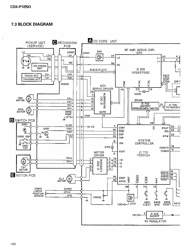
7.3 BLOCK DIAGRAM
AC
D
E
49
CDX-P1250
B
CDX-P1250
8. OPERATIONS AND SPECIFICATIONS
8.1 OPERATION
If the power does not switch on or if the compact disc player doesnot operate when the button on the multi-CD controller is pressed,or if the multi-CD controller display is incorrect, press this button onthe player with the tip of a pencil to restore normal operation. (Thisbutton is located inside the door.) Always press the clear button onthe multi-CD controller, too, after pressing this button.• If the clear button is pressed when the player contains a magazine
or the ignition switch is set to the ON or ACC position, the CD titledisplay and ITS memory are cleared.