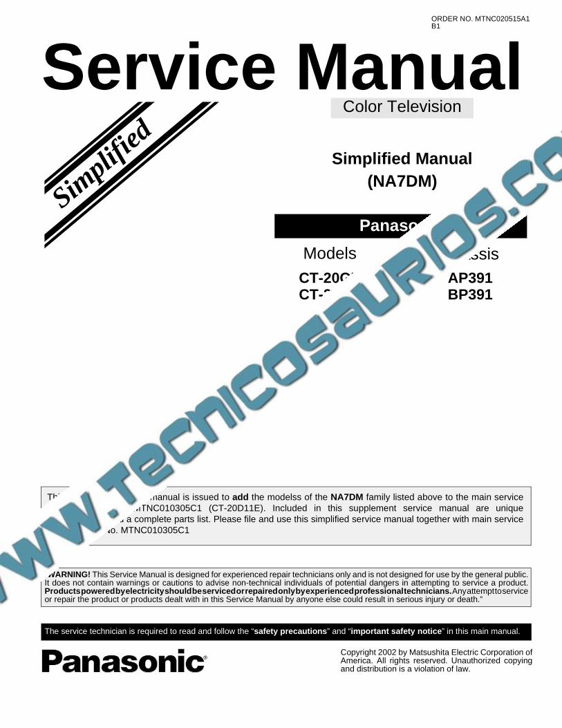
Panasonic The service technician is required to read and follow the “safety precautions” and “important safety notice” in this main manual. Service Manual Color Television (NA7DM) Simplified Manual Copyright 2002 by Matsushita Electric Corporation of America. All rights reserved. Unauthorized copying and distribution is a violation of law. “WARNING! This Service Manual is designed for experienced repair technicians only and is not designed for use by the general public. It does not contain warnings or cautions to advise non-technical individuals of potential dangers in attempting to service a product. Productspoweredbyelectricityshouldbeservicedorrepairedonlybyexperiencedprofessionaltechnicians. Anyattempttoservice or repair the product or products dealt with in this Service Manual by anyone else could result in serious injury or death.” Chassis CT-20G7DF AP391 CT-20D12DF BP391 Models ORDER NO. MTNC020515A1 B1 This supplement service manual is issued to add the modelss of the NA7DM family listed above to the main service manual order No. MTNC010305C1 (CT-20D11E). Included in this supplement service manual are unique characteristics and a complete parts list. Please file and use this simplified service manual together with main service manual order No. MTNC010305C1 Simplified
Transcript
Panasonic
The service technician is required to read and follow the “safety precautions ” and “important safety notice ” in this main manual.
Service ManualColor Television
(NA7DM)Simplified Manual
Copyright 2002 by Matsushita Electric Corporation ofAmerica. All rights reserved. Unauthorized copyingand distribution is a violation of law.
“WARNING! This Service Manual is designed for experienced repair technicians only and is not designed for use by the general public.It does not contain warnings or cautions to advise non-technical individuals of potential dangers in attempting to service a product.Productspoweredbyelectricityshouldbeservicedorrepairedonlybyexperiencedprofessionaltechnicians. Anyattempttoserviceor repair the product or products dealt with in this Service Manual by anyone else could result in serious injury or death.”
ChassisCT-20G7DF AP391CT-20D12DF BP391
Models
ORDER NO. MTNC020515A1B1
This supplement service manual is issued to add the modelss of the NA7DM family listed above to the main servicemanual order No. MTNC010305C1 (CT-20D11E). Included in this supplement service manual are uniquecharacteristics and a complete parts list. Please file and use this simplified service manual together with main servicemanual order No. MTNC010305C1
Simplif
ied
- 2 -
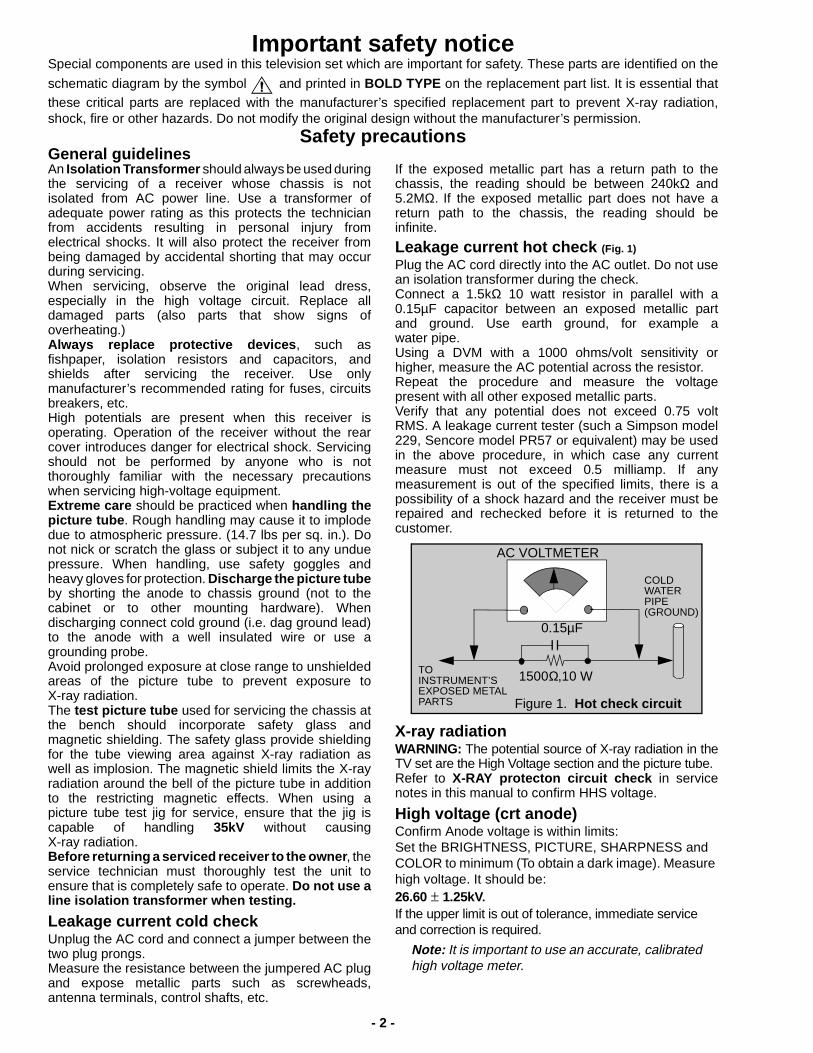
Important safety noticeSpecial components are used in this television set which are important for safety. These parts are identified on the
schematic diagram by the symbol and printed in BOLD TYPE on the replacement part list. It is essential thatthese critical parts are replaced with the manufacturer’s specified replacement part to prevent X-ray radiation,shock, fire or other hazards. Do not modify the original design without the manufacturer’s permission.
Safety precautionsGeneral guidelinesAn Isolation Transformer should always be used duringthe servicing of a receiver whose chassis is notisolated from AC power line. Use a transformer ofadequate power rating as this protects the technicianfrom accidents resulting in personal injury fromelectrical shocks. It will also protect the receiver frombeing damaged by accidental shorting that may occurduring servicing.When servicing, observe the original lead dress,especially in the high voltage circuit. Replace alldamaged parts (also parts that show signs ofoverheating.)Always replace protective devices , such asfishpaper, isolation resistors and capacitors, andshields after servicing the receiver. Use onlymanufacturer’s recommended rating for fuses, circuitsbreakers, etc.High potentials are present when this receiver isoperating. Operation of the receiver without the rearcover introduces danger for electrical shock. Servicingshould not be performed by anyone who is notthoroughly familiar with the necessary precautionswhen servicing high-voltage equipment.Extreme care should be practiced when handling thepicture tube . Rough handling may cause it to implodedue to atmospheric pressure. (14.7 lbs per sq. in.). Donot nick or scratch the glass or subject it to any unduepressure. When handling, use safety goggles andheavy gloves for protection. Discharge the picture tubeby shorting the anode to chassis ground (not to thecabinet or to other mounting hardware). Whendischarging connect cold ground (i.e. dag ground lead)to the anode with a well insulated wire or use agrounding probe.Avoid prolonged exposure at close range to unshieldedareas of the picture tube to prevent exposure toX-ray radiation.The test picture tube used for servicing the chassis atthe bench should incorporate safety glass andmagnetic shielding. The safety glass provide shieldingfor the tube viewing area against X-ray radiation aswell as implosion. The magnetic shield limits the X-rayradiation around the bell of the picture tube in additionto the restricting magnetic effects. When using apicture tube test jig for service, ensure that the jig iscapable of handling 35kV without causingX-ray radiation.Before returning a serviced receiver to the owner , theservice technician must thoroughly test the unit toensure that is completely safe to operate. Do not use aline isolation transformer when testing.
Leakage current cold checkUnplug the AC cord and connect a jumper between thetwo plug prongs.Measure the resistance between the jumpered AC plugand expose metallic parts such as screwheads,antenna terminals, control shafts, etc.
If the exposed metallic part has a return path to thechassis, the reading should be between 240kΩ and5.2MΩ. If the exposed metallic part does not have areturn path to the chassis, the reading should beinfinite.
Leakage current hot check (Fig. 1)
Plug the AC cord directly into the AC outlet. Do not usean isolation transformer during the check.Connect a 1.5kΩ 10 watt resistor in parallel with a0.15µF capacitor between an exposed metallic partand ground. Use earth ground, for example awater pipe.Using a DVM with a 1000 ohms/volt sensitivity orhigher, measure the AC potential across the resistor.Repeat the procedure and measure the voltagepresent with all other exposed metallic parts.Verify that any potential does not exceed 0.75 voltRMS. A leakage current tester (such a Simpson model229, Sencore model PR57 or equivalent) may be usedin the above procedure, in which case any currentmeasure must not exceed 0.5 milliamp. If anymeasurement is out of the specified limits, there is apossibility of a shock hazard and the receiver must berepaired and rechecked before it is returned to thecustomer.
X-ray radiationWARNING: The potential source of X-ray radiation in theTV set are the High Voltage section and the picture tube.Refer to X-RAY protecton circuit check in servicenotes in this manual to confirm HHS voltage.
High voltage (crt anode)Confirm Anode voltage is within limits:Set the BRIGHTNESS, PICTURE, SHARPNESS andCOLOR to minimum (To obtain a dark image). Measurehigh voltage. It should be:26.60 ± 1.25kV.If the upper limit is out of tolerance, immediate serviceand correction is required.
Note: It is important to use an accurate, calibratedhigh voltage meter.
Leadless chip component(surface mount)Chip components must be replaced with identical chipsdue to critical foil track spacing. There are no holes inthe board to mount standard transistors or diodes.Some chips capacitor or resistor board solder padsmay have holes through the board, however the holediameter limits standard resistor replacement to 1/8watt. Standard capacitor may also be limited for thesame reason. It is recommended that identicalcomponents be used.Chip resistor have a three digit numerical resistancecode - 1st and 2nd significant digits and a multiplier.Example: 162 = 1600 or 1.6kΩ resistor, 0 = 0Ω (jumper).Chip capacitors generally do not have the valueindicated on the capacitor. The color of the componentindicates the general range of the capacitance.Chip transistors are identified by a two letter code. Thefirst letter indicates the type and the second letter, thegrade of transistor.Chip diodes have a two letter identification code as perthe code chart and are a dual diode pack with eithercommon anode or common cathode. Check the partslist for correct diode number.
Component removal1. Use solder wick to remove solder from component
end caps or terminal.2. Without pulling up, carefully twist the component
with tweezers to break the adhesive.3. Do not reuse removed leadless or chip
components since they are subject to stressfracture during removal.
Chip component Installation1. Put a small amount of solder on the board
soldering pads.2. Hold the chip component against the soldering
pads with tweezers or with a miniature alligator clipand apply heat to the pad area with a 30 watt ironuntil solder flows. Do not apply heat for more than3 seconds.
How to replace Flat-IC- Required tools -
1. Cut the pins of the defective IC with the wire cutterspliers, and remove it completely away from theboard. If the IC is glued to the board, apply hot airto complete the removal. CAUTION- Do not pull ortwist the pliers, may damage the soldering pads inthe board.
2. Using the soldering Iron and the long nose pliers,remove the IC pins that still attached to the board.
3. Using the de-solder braid and the soldering iron,remove the solder from the board soldering pads.
4. Position the new Flat-IC in place (apply the pins ofthe Flat-IC to the soldering pads where the pinsneed to be soldered). Properly determine thepositions of the soldering pads and pins bycorrectly aligning the polarity symbol. Start aligningand soldering pin no.1, then align and solder thepin in the apposite corner of the IC, this will help toalign the rest of the pins.
5. Solder all pins to the soldering pads using a finetipped soldering iron.
6. Check with a magnifier for solder bridge betweenthe pins or for dry joint between pins and solderingpads. To remove a solder bridge, use a de-solderbraid as shown in the figure below.
Note: These components are affixed with glue. Be careful not to break or damage any foil under thecomponent or at the pins of the ICs when removing. Usually applying heat to the component for a short timewhile twisting with tweezers will break the component loose.
c
b
e
Chip components
TRANSISTOR CAPACITOR
RESISTORMH DIODE
SOLDERCAPS
SOLDERCAPS
1ST DIGIT 2ND DIGIT
MULTIPLIER=1600 = 1.6k
GRADE
TYPE
COMMON
ANODES
CATHODE
• Soldering iron • De-solder braids
• Sharpen pliers (wirecutters and long nose)
• Magnifier
Flat-IC
Solderingiron
De-Solderbraid
Solderingiron
Polaritysymbol
Solderingiron
Solder
De-Solderbraid
Solderbridge
Solderingiron
- 5 -
Service notes (continued)IMPORTANT: To protect against possible damage tothe solid state devices due to arcing or static discharge,make certain that all ground wires and CTR DAG wireare securely connected.
CAUTION: The power supply circuit is above earthground and the chassis cannot be polarized. Use anisolation transformer when servicing the receiver toavoid damage to the test equipment or to the chassis.Connect the test equipment to the proper ground ( ) or( ) when servicing, or incorrect voltages will bemeasured.
WARNING: This receiver has been designed to meetor exceed applicable safety and x-ray radiationprotection as specified by government agencies andindependent testing laboratories.
To maintain original product safety design standardsrelative to x-ray radiation and shock and fire hazard,
parts indicated with the symbol on the schematicmust be replaced with identical parts. Order parts fromthe manufacturer’s parts center using the partsnumbers shown in this service manual, or provide thechassis number and the part reference number.
For optimum performance and reliability, all other partsshould be replaced with components ofidentical specification.
X-ray protection circuit checkThis test must be performed as final check before thereceiver is returned to the customer. If voltage is out oftolerance, immediate service and correction is requiredto insure safe operation and to prevent the possibility ofpremature component failure.
Equipment needed to check the protection circuit:
1. Isolator transformer.2. High voltage meter.3. Short jumper.4. Diode connection jumper.
Use similar diode than D823, refer to parts list forpart No., (diode should support at least 150V.)
Procedure:1. Connect receiver to isolator transformer.2. Apply a monoscope pattern.3. In service mode. (Refer to service mode section)
select register C0b.4. Measure TP5 (TPs port close to tuner). Compare
the measure of TP5 and set the data for C0baccording the following table
5. Exit service mode and turn receiver OFF.6. Connect a jumper from TPD16 to TPD17.7. Connect the diode jumper, cathode to TPD14
(cold GND), anode to TPD15 (hot GND).Note: Refer to Fig. 2 for test point location.
8. Apply 75V AC to the AC input of the Insulatortransformer.Turn receiver ON.
9. Set PICTURE and BRIGTHNESS to minimum.10. Increase the AC voltage at the input of Insulator
transformer and confirm the HHS voltage is32.0kV, at the point set starts to loose sync,
11. Reset picture controls to original levels.12. Turn the set OFF, and remove all jumpers and
connections from chassis.
TP5MEASURE (V)
DATA TOC0b (Hex)
0 ~ 0.93 00
0.93 ~ 0.97 01
0.97 ~ 1.01 02
1.01 ~ 1.05 03
1.05 ~ 1.09 04
1.09 ~ 1.13 05
1.13 ~ 1.17 06
1.17 ~ 1.21 07
- 6 -
Receiver feature table
*Note: When ordering a board, add and ” S” after the board suffix application.Example, If order A-Board for CT-20G7DF, should be ordered as: TNP2AH040DHS.
FEATURE\MODEL CT-20G7DF CT-20D12DF
Chassis No AP391 BP391
Family NA7DM
Number of channels 181
Menu language Eng/Span/Fr
Closed Caption X
V-Chip X
75 Ω input X
Remote Model number EUR501450 EUR511502
Picture tube type PANABLACK
Picture tube Supplier SAMSUNG
Comb Filter 2 DIG
V/A norm V
FM Radio ---- X
MTS/SAP/DBX X
Built-in audio power 1.5Wx2 (10%)
Number of speakers 2
AI Sound X
A/V in (rear/front) 1(1/1)
Audio Out (F:FAO/V:VAO) --- F,V
S-VHS In (rear/front) --- 1/0
EPJ/HPJ/MISC HPJ
Dimensions mm(WxDxH) in
515.7x490.5x461.720.30x19.31x18.17
Weight (kg/lbs) 18/39.6
Anode voltage 26.60 ± 1.25 kV
Video input jack 1Vp-p 75Ω, phono
Audio input jack 500mV rms, 47KΩ
A-Board TNP2AH040 DH* DK*
C-Board TNP2AA106 AF*
Table 1. Receiver features
Specifications are subject to change without notice or obligation.Dimensions and weights are approximate.
- 7 -
Chasis service adjustment proceduresAll service adjustments are factory preset and should not require adjustment unless controls and/orassociated components are replaced.
Note: Connect the (-) lead of the voltmeter to the appropriate ground. Use IC801’s heat sink when the HOTground symbol ( ) is used. Otherwise, use COLD ground ( ) — tuner shield, IC451’s heat sink or FA2.
COMPONENTS WITHIN DOT LINES ARE LOCATED AT THE OPOSITE SIDE OF BOARD.
130.0V B+ voltage confirmation1. Set the BRIGHT and the PICTURE to minimum by
using the PICTURE menu.2. Connect the DVM between C825 (+ side) and cold
ground ( ).3. Confirm that B+ voltage is 130.0V ± 2.5V. This
voltage supplies B+ to the horizontal output &flyback circuits.
Source voltage chart120V AC line input. Set the BRIGHT and the PICTUREto minimum by using the PICTURE menu. Use coldground ( ) for the (-) lead of the DVM.
Adjust PICTURE menu for normalized videoadjustments.
High voltage check1. Select an active TV channel and confirm that the
horizontal is in sync.2. Adjust BRIGHTNESS and PICTURE using picture
icon menu, so video just disappears.3. Confirm B+ 130V is within limit.4. Using a high voltage meter confirm that the high
voltage is:26.60kV±1.25kV
Figure 2. A-Board maincomponentsand test points
TPD8
SCREENFOCUS
IC552
IC551
COLD ( )
HOT ( )
F801
D554
IC451A11
IC001
IC801
C825
FA1
DATA
CLK
FA2
TPD9
D561
IC003IC002
CRTGND
IC2301
IC2302
IC050
TPD16
TPD15
TPD17
TPD14
TPE11
TPE10TUNER
LOCATION VOLTAGE
TPD8 26.0V ± 2V
TPD9 25.0V ± 2V
IC552 Pin3 5.0V ± 0.25V
IC551 Pin3 9.0V ± 0.25V
D554 Cathode 200V ± 15V
LOCATION VOLTAGE
- 8 -
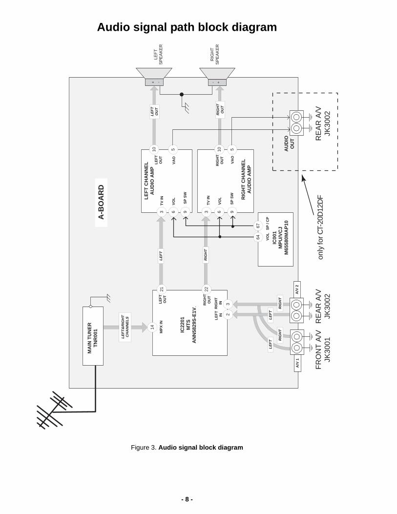
Audio signal path block diagram
Figure 3. Audio signal block diagram
MA
IN T
UN
ER
TN
R00
1
A/V
2
IC22
01M
TS
AN
N58
29S
-E1V
.
LEF
T&
RIG
HT
CH
AN
NE
LS
14
23
A/V
1
LEF
TLE
FT
RIG
HT
RIG
HT
LE
FT
INR
IGH
T IN
MP
X IN
FR
ON
T A
/VJK
3001
RE
AR
A/V
JK30
02
IC00
1M
PU
/VC
JM
6558
0MA
P10
2221LE
FT
RIG
HT
LE
FT
OU
T
RIG
HT
OU
T
64
LE
FT
CH
AN
NE
LA
UD
IO A
MP
3 6
RIG
HT
CH
AN
NE
LA
UD
IO A
MP
3 69 9
TV
IN
67
VO
L
SP
SW
VO
L
TV
IN
VO
L
SP
SW
SP
/ C
P
RE
AR
A/V
JK30
02
LEF
TS
PE
AK
ER
RIG
HT
SP
EA
KE
R
+ - +-
5 510 10
LEF
TO
UT
RIG
HT
OU
T
A-B
OA
RD
LE
FT
OU
T
RIG
HT
OU
T
VA
O
VA
O
AU
DIO
OU
T
on
ly fo
r CT-
20D
12D
F
- 9 -
Video signal path block diagram
Figure 4. Video signal block diagram
MA
IN T
UN
ER
TN
R00
1
A/V
2
26
A/V
1
TV
IN
FR
ON
T A
/VJK
3001
RE
AR
A/V
JK30
02
IC00
1M
PU
/VC
JM
6558
0MA
P10
A-B
OA
RD
20EX
T
59
6
23
9
41
8
Q00
6
Q00
7
Q00
83228 30
HA
LF
-T
ON
E
R-O
UT
G-O
UT
B-O
UT
5 13
IC05
0H
AL
FT
ON
E
3.3V
Q05
3
Q05
4
Q05
5
28 FB
A11 1 2 3
C1 1 2 3
Q35
4 -R
Q35
5 -G
Q35
6 -B
Q35
1 -R
Q35
2 -G
Q35
3 -B
C-B
OA
RD
V ID
EO
IN
V ID
EO
IN4849
51
Q05
0Q
053
Q05
3
OS
DR
R
GB
22 24 72
JK30
01
Y IN
C IN
SS
W
on
ly fo
r CT-
20D
12D
F
- 10 -Parts List
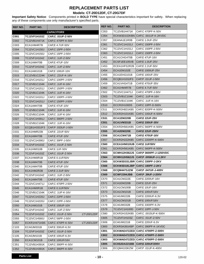
REPLACEMENT PARTS LISTModels: CT-20D12DF, CT-20G7DF
Important Safety Notice : Components printed in BOLD TYPE have special characteristics important for safety. When replacingany of these components use only manufacturer’s specified parts.
120-02
PA
RT
SLIS
T
REF NO. PART NO. DESCRIPTION
CAPACITORS
C001 TCJ2VF1H103Z CAP,C .01UF-Z-50V
C002 TCJ2VB1H471K CAP,C 470PF-K-50V
C003 ECA1HM4R7B CAP,E 4.7UF-50V
C004 TCJ2VC1H150J CAP,C 15PF-J-50V
C005 TCJ2VC1H150J CAP,C 15PF-J-50V
C008 TCJ2VF1H104Z CAP,C .1UF-Z-50V
C009 ECA1AM470B CAP,E 47UF-10V
C010 TCJ2VF1H104Z CAP,C .1UF-Z-50V
C011 ECA1AM101B CAP,E 100UF-10V
C015 ECJ2VB1C224K CAP,C .22UF-K-16V
C016 TCJ2VC1H101J CAP,C 100PF-J-50V
C017 TCJ2VB1C104K CAP,C .1UF-K-16V
C018 TCJ2VC1H151J CAP,C 150PF-J-50V
C020 TCJ2VB1C104K CAP,C .1UF-K-16V
C022 TCJ2VC1H101J CAP,C 100PF-J-50V
C023 TCJ2VC1H151J CAP,C 150PF-J-50V
C024 ECA1AM470B CAP,E 47UF-10V
C025 TCJ2VB1C104K CAP,C .1UF-K-16V
C026 TCJ2VB1C104K CAP,C .1UF-K-16V
C027 TCJ2VC1H391J CAP,C 390PF-J-50V
C028 TCJ2VB1C104K CAP,C .1UF-K-16V
C029 ECQB1H333JF3 CAP,P .033UF-J-50V
C031 ECA1HMR22B CAP,E .22UF-50V
C032 ECA1AM470B CAP,E 47UF-10V
C033 TCJ2VC1H390J CAP,C 39PF-J-50V
C034 TCJ2VF1H103Z CAP,C .01UF-Z-50V
C035 ECA1HM010B CAP,E 1UF-50V
C036 TCJ2VF1H103Z CAP,C .01UF-Z-50V
C037 ECA1HM0R1B CAP,E 0.1UF/50V
C038 ECA1AM470B CAP,E 47UF-10V
C040 ECA1AM470B CAP,E 47UF-10V
C041 ECA1HM2R2B CAP,E 2.2UF-50V
C042 TCJ2VF1H104Z CAP,C .1UF-Z-50V
C043 ECA1AM470B CAP,E 47UF-10V
C044 TCJ2VC1H471J CAP,C 470PF-J-50V
C045 ECA1HM0R1B CAP,E 0.1UF/50V
C046 TCJ2VB1C104K CAP,C .1UF-K-16V
C047 TCJ2VC1H220J CAP,C 22PF-J-50V
C048 TCJ2VC1H220J CAP,C 22PF-J-50V
C050 ECA1AM101B CAP,E 100UF-10V
C051 TCJ2VF1H104Z CAP,C .1UF-Z-50V
C054 TCJ2VF1H103Z CAP,C .01UF-Z-50V CT-20D12DF
C055 TCJ2VC1H560J CAP,C 56PF-J-50V
C057 ECKR1H471KB5 CAP,C 470PF-K-50V CT-20D12DF
C103 ECA0JM331B CAP,E 330UF-6.3V
C104 TCJ2VF1H103Z CAP,C .01UF-Z-50V
C105 ECA0JM101B CAP,E 100UF-6.3V
C350 ECA1CM101B CAP,E 100UF/16V
C351 TCJ2VB1H391K CAP,C 390PF-K-50V
C352 TCJ2VB1H391K CAP,C 390PF-K-50V
C353 TCJ2VB1H471K CAP,C 470PF-K-50V
C354 ECKW3D102KBN CAP,C .001UF-K-2KVDC
C357 EEANA1E1R0B CAP,E 1.0UF-25V
C361 TCJ2VC1H151J CAP,C 150PF-J-50V
C362 TCJ2VC1H151J CAP,C 150PF-J-50V
C363 TCJ2VC1H151J CAP,C 150PF-J-50V
C451 ECA1CHG470B CAP,E 47UF-16V
C452 ECSF1EE105VB CAP,E 1.0UF-25V
C453 ECEA1HFS2R2B CAP,E 2.2UF-50V
C454 ECA1EM102E CAP,E 1000UF-25V
C455 ECA1EHG101B CAP,E 100UF-25V
C456 ECQB1H103JF3 CAP,P .01UF-J-50V
C459 ECA1VHG471B CAP,E 470UF-35V
C462 ECA1HM4R7B CAP,E 4.7UF-50V
C502 TCJ2VC1H471J CAP,C 470PF-J-50V
C503 TCJ2VB1C104K CAP,C .1UF-K-16V
C504 TCJ2VB1C104K CAP,C .1UF-K-16V
C510 ECCR2H100D5 CAP,C 10PF-D-500V
C511 ECKR2H821KB5 CAP,C 820PF-K-500V
C512 ECKR2H101KB5 CAP,C 100UF-K-500V
C531 ECA1EM220B CAP,E 22UF-25V
C551 ECA1VM331B CAP,E 330UF-35V
C554 ECKR2H561KB5 CAP,C 560PF-K-500V
C555 ECA2EM220E CAP,E 22UF-250V
C556 ECA1CM471B CAP,E 470UF-16V
C557 ECKR2H222KB5 CAP,C 2200PF-K-500V
C560 ECEA1HN010UB CAP,E 1UF/50V
C561 ECKR2H561KB5 CAP,C 560PF-K-500V
C563 ECWH12H362JS CAP,P 3600PF-J-1250VDC
C564 ECWH12H562JS CAP,P .0056UF-J-1.2KV
C565 ECKW3D331JBR CAP,C 330PF-J-2KV
C566 ECKW3D181JBP CAP,C 180PF-J-2KV
C568 ECQM4473JZW CAP,P .047UF-J-400V
C569 ECWF2394JBB CAP,P .39UF-J-200V
C570 ECA1CM222E CAP,E 2200UF-16V
C571 ECA1EM220B CAP,E 22UF-25V
C572 ECA1CM100B CAP,E 10UF-16V
C573 ECA1CM101B CAP,E 100UF/16V
C575 ECA0JM222B CAP,E 2200UF-6.3V
C577 ECA1CM101B CAP,E 100UF/16V
C578 ECA0JM332B CAP,E 3300PF-6.3V
C579 TCJ2VC1H100D CAP,C 10PF-J-50V
C580 ECKR2H152KB5 CAP,C .0015UF-K-500V
C605 TCJ2VF1H103Z CAP,C .01UF-Z-50V
C606 ECA0JM221B CAP,E 220UF-6.3V
C800 ECKR3A391KBP CAP,C 390PF-K-1KVDC
C801 ECKWAE472ZED CAP,C 4700PF-Z-500V
C802 ECKWAE472ZED CAP,C 4700PF-Z-500V
C803 ECKWAE472ZED CAP,C 4700PF-Z-500V
C805 EC0S2DA221BB CAP,E 220UF/200V
C806 ECQM4103KZW CAP,P .01UF-K-400V
REF NO. PART NO. DESCRIPTION
REPLACEMENT PARTS LISTModels: CT-20D12DF, CT-20G7DF
Important Safety Notice : Components printed in BOLD TYPE have special characteristics important for safety. When replacingany of these components use only manufacturer’s specified parts.
- 11 -120-02
PA
RT
SLI
ST
Parts List
C807 ECKR3A821KBP CAP,C 820PF-K-1KV
C808 ECA1VM101B CAP,E 100UF-35V
C809 ECKR1H101KB5 CAP,C 100PF-K-50V
C810 ECKR1H471KB5 CAP,C 470PF-K-50V
C812 ECQU2A224MVA CAP,P .22UF-M-250VAC
C813 ECQU2A153MVA CAP,P .015UF-M-250VAC
C814 ECQU2A153MVA CAP,P .015UF-M-250VAC
C820 ECA1CM101B CAP,E 100UF/16V
C821 TCJ2VF1H103Z CAP,C .01UF-Z-50V
C822 ECKR3A221KBP CAP,C 220PF-K-1KV
C823 ECA1VM471E CAP,E 470UF-35V
C824 ECKR3A102KBP CAP,C 1000PF-K-1KV
C825 EEUMG2C221S CAP,E 220UF-160V
C826 ECKR3A471KBP CAP,C 470PF-K-1KV
C827 ECA1CM471B CAP,E 470UF-16V
C828 ECA160V33UE CAP,E 33UF/160V
C2201 ECA1HM4R7B CAP,E 4.7UF-50V
C2202 ECA1HM2R2B CAP,E 2.2UF-50V
C2203 ECA1HM4R7B CAP,E 4.7UF-50V
C2204 AP106K016CAE CAP,T 10UF/16V
C2205 ECA1HMR33B CAP,E .33UF-50V
C2206 ECQB1H223JF3 CAP,P .022UF-J-50V
C2207 AP335K016CAE CAP,T 3.3UF/16V
C2208 TCJ2VB1C104K CAP,C .1UF-K-16V
C2209 TCJ2VB1C104K CAP,C .1UF-K-16V
C2210 TCJ2VB1C104K CAP,C .1UF-K-16V
C2212 ECQB1H473JF3 CAP,P .047UF-J-50V
C2213 ECA1HMR47B CAP,E .47UF-50V
C2214 ECA1AM101B CAP,E 100UF-10V
C2215 EEANA1E100B CAP,E 10UF-25V
C2216 TCJ2VC1H100D CAP,C 10PF-J-50V
C2301 ECA1EM102E CAP,E 1000UF-25V
C2302 ECEA1HN010UB CAP,E 1UF/50V
C2303 ECA1EM101B CAP,E 100UF-25V
C2304 ECA1CM100B CAP,E 10UF-16V
C2307 ECA1CM102B CAP,E 1000UF/16V
C2309 ECA1HM010B CAP,E 1UF-50V CT-20D12DF
C2311 ECA1EM102E CAP,E 1000UF-25V
C2312 ECEA1HN010UB CAP,E 1UF/50V
C2313 ECA1EM101B CAP,E 100UF-25V
C2314 ECA1CM100B CAP,E 10UF-16V
C2317 ECA1CM102B CAP,E 1000UF/16V
C2319 ECA1HM010B CAP,E 1UF-50V CT-20D12DF
C2320 ECA1CM100B CAP,E 10UF-16V
C2330 ECA1CM100B CAP,E 10UF-16V
C2350 ECA1HM100B CAP,E 10UF/50V
C3001 ECA1HM0R1B CAP,E 0.1UF/50V
C3012 ECA1HM010B CAP,E 1UF-50V
C3018 ECA1HM010B CAP,E 1UF-50V
C3050 TCJ2VF1H103Z CAP,C .01UF-Z-50V CT-20D12DF
C3051 TCJ2VF1H103Z CAP,C .01UF-Z-50V CT-20D12DF
REF NO. PART NO. DESCRIPTION
DIODES
D002 MA165TA5VT DIODE, SWITCHING
D006 MA4330HTA DIODE
D052 MA4068MTA DIODE, ZENER
D053 MA4056MTA DIODE
D055 MA4056MTA DIODE
D451 ERA15-01V3 DIODE, RECTIFIER
D452 MA4047MTA DIODE
D453 MA165TA5VT DIODE, SWITCHING
D454 MA165TA5VT DIODE, SWITCHING
D456 MA4047MTA DIODE
D502 MA4047MTA DIODE
D531 AS01V0 DIODE
D551 D1NL20UV70 DIODE
D554 AU02V0 DIODE
D558 RS3FS DIODE
D559 BYD33G-113 DIODE
D561 AU02V0 DIODE
D571 MA165TA5VT DIODE, SWITCHING
D606 MA165TA5VT DIODE, SWITCHING
D607 MA152KTX DIODE
D608 MA152KTX DIODE
D609 MA152KTX DIODE
D801 D3SBA60-4103 DIODE
D806 TAP2AA0001 PTC 5-OHM
D808 SARS01V1 DIODE
D809 AG01V0 DIODE
D810 AG01V0 DIODE
D811 AG01V0 DIODE
D812 MA4068MTA DIODE, ZENER
D820 MA165TA5VT DIODE, SWITCHING
D821 MA4047HTA DIODE
D822 RN1ZLF-B1 DIODE
D823 S3L60P154004 DIODE
D824 D1NL20UV70 DIODE
D2305 MA3110MTX DIODE, ZENER CT-20D12DF
D2306 MA3110MTX DIODE, ZENER CT-20D12DF
D2307 MA3110MTX DIODE, ZENER CT-20D12DF
D2308 MA3110MTX DIODE, ZENER CT-20D12DF
D2350 MA4068MTA DIODE, ZENER
D2351 MA165TA5VT DIODE, SWITCHING
D2352 MA165TA5VT DIODE, SWITCHING
D2353 MA165TA5VT DIODE, SWITCHING
D2354 MA4091MTA DIODE
D3001 MA3110MTX DIODE, ZENER
D3003 MA3110MTX DIODE, ZENER
D3004 MA3110MTX DIODE, ZENER
D3005 MA3110MTX DIODE, ZENER
D3006 MA3110MTX DIODE, ZENER
D3017 MA3110MTX DIODE, ZENER
D3018 MA3110MTX DIODE, ZENER
REF NO. PART NO. DESCRIPTION
- 12 -Parts List
REPLACEMENT PARTS LISTModels: CT-20D12DF, CT-20G7DF
Important Safety Notice : Components printed in BOLD TYPE have special characteristics important for safety. When replacingany of these components use only manufacturer’s specified parts.
120-02
PA
RT
SLIS
T
D3019 MA3110MTX DIODE, ZENER
D3020 MA3110MTX DIODE, ZENER
D3021 MA3110MTX DIODE, ZENER
D3022 MA3110MTX DIODE, ZENER
FUSES
F801 XBA2A00101 FUSE 6.3A 125V
INTEGRATED CIRCUITS
IC001 M65580MAP103 MPU/VCJ
IC002 TVR2AJ125 EEPROM
IC003 PIC-37042SR IR RECEIVER
IC005 PQ1X331M2ZP VOLTAGE REGULATOR, 3.3V
IC006 MN1280R RESET
IC050 TC74HC4066AL HALFTONE
IC451 LA7837-TV V-OUT
IC551 AN78L09 INT CKT CT-20D12DF
IC551 AN78M09LB VOLTAGE REGULATOR 9V CT-20G7DF
IC552 AN78M05LB VOLTAGE REGULATOR, 5V
IC553 AN78M05LB VOLTAGE REGULATOR, 5V
IC801 STRG5623A POWER SUPPLY, 360V
IC2201 AN5829S-E1V MTS, S-AGC
IC2301 AN17800A AUDIO AMP CT-20G7DF
IC2301 AN17801A AUDIO AMP CT-20D12DF
IC2302 AN17800A AUDIO AMP CT-20G7DF
IC2302 AN17801A AUDIO AMP CT-20D12DF
COILS
L001 EXCELSA35T FERRITE BEAD
L003 TLUABTA2R2K COIL, PEAKING 2.2UH
L004 TLUABTA2R2K COIL, PEAKING 2.2UH
L005 EXCELDR35V FERRITE BEAD
L006 EXCELSA24T FERRITE BEAD
L007 EXCELDR35V FERRITE BEAD
L008 TLUABTA470K COIL, PEAKING 47UH
L009 EXCELSA35V FERRITE BEAD
L010 ELESN330JA COIL, PEAKING 33UH
L011 ELESN330JA COIL, PEAKING 33UH
L013 EXCELDR35V FERRITE BEAD
L014 ELESN180KA COIL, PEAKING 18UH
L015 EXCELSA35V FERRITE BEAD
L016 EXCELSA35V FERRITE BEAD
L017 TLUABTA100K COIL, PEAKING 10UH
L018 TLUABTA150K COIL, PEAKING 15UH
L019 EXCELDR35V FERRITE BEAD
L090 EXCELSA24T FERRITE BEAD
L104 TLUABTA2R2K COIL, PEAKING 2.2UH
L108 EXCELSA35V FERRITE BEAD
L238 EXCELSA39V FERRITE BEAD
L245 EXCELSA35V FERRITE BEAD
L250 EXCELSA35V FERRITE BEAD
L306 TLUABTA2R2K COIL, PEAKING 2.2UH
L325 EXCELSA35V FERRITE BEAD
L403 TLUABTA2R2K COIL, PEAKING 2.2UH
REF NO. PART NO. DESCRIPTION
L416 EXCELSA39V FERRITE BEAD
L551 ELH5L4101 COIL
L801 ELF15N011A COIL, PEAKING
L802 ELEIE680KA COIL, PEAKING 68UH
L803 TALL08T680KA COIL
L2305 EXCELSA35V FERRITE BEAD
L2308 EXCELSA24V FERRITE BEAD
L2350 ELESN4R7JA COIL, PEAKING 4.7UH
TRANSISTORS
Q001 2SD601ARTX TRANSISTOR
Q006 2SB709ARTX TRANSISTOR
Q007 2SB709ARTX TRANSISTOR
Q008 2SB709ARTX TRANSISTOR
Q009 2SC1473A TRANSISTOR
Q050 2SB709ARTX TRANSISTOR
Q051 2SB709ARTX TRANSISTOR
Q052 2SB709ARTX TRANSISTOR
Q053 2SD601ARTX TRANSISTOR
Q054 2SD601ARTX TRANSISTOR
Q055 2SD601ARTX TRANSISTOR
Q090 2SB709ARTX TRANSISTOR
Q092 2SB709ARTX TRANSISTOR
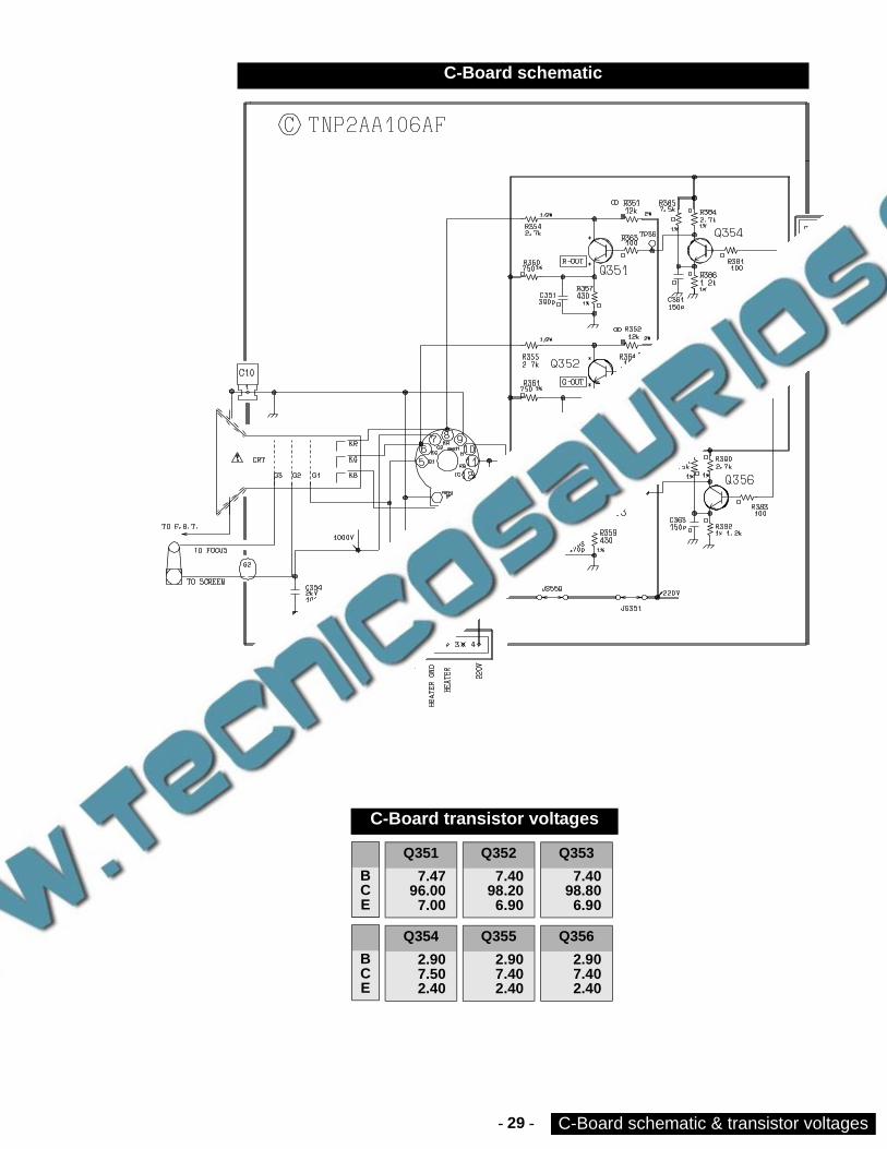
Q351 2SC3063RL TRANSISTOR
Q352 2SC3063RL TRANSISTOR
Q353 2SC3063RL TRANSISTOR
Q354 2SD601ARTX TRANSISTOR
Q355 2SD601ARTX TRANSISTOR
Q356 2SD601ARTX TRANSISTOR
Q451 2SD601ARTX TRANSISTOR
Q452 2SD601ARTX TRANSISTOR
Q453 2SD601ARTX TRANSISTOR
Q501 2SC1573AH TRANSISTOR
Q505 2SD601ARTX TRANSISTOR
Q520 2SD601ARTX TRANSISTOR
Q551 2SC562200VLA TRANSISTOR
Q605 2SB709ARTX TRANSISTOR
Q606 2SD601ARTX TRANSISTOR
Q820 2SA1767QTA TRANSISTOR
Q830 2SB1011QRL TRANSISTOR
Q2350 2SB709ARTX TRANSISTOR
RELAYS
RL801 TSEH0005 RELAY
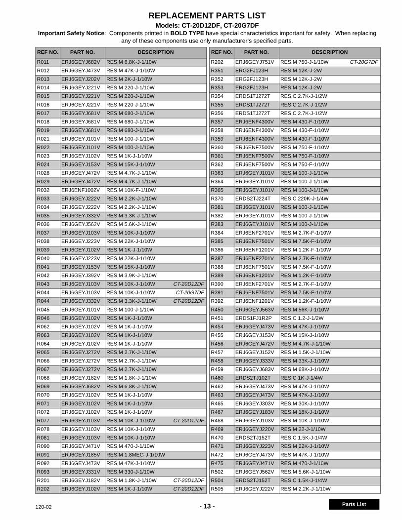
RESISTORS
R001 ERJ6GEYJ102V RES,M 1K-J-1/10W
R003 ERJ6GEYJ105V RES,M 1M-J-1/10W
R004 ERJ6GEYJ562V RES,M 5.6K-J-1/10W
R006 ERDS2TJ101T RES,C 100-J-1/4W
R007 ERJ6GEYJ471V RES,M 470-J-1/10W
R008 ERJ6GEYJ471V RES,M 470-J-1/10W
R009 ERJ6GEYJ472V RES,M 4.7K-J-1/10W
R010 ERJ6GEYJ682V RES,M 6.8K-J-1/10W
REF NO. PART NO. DESCRIPTION
REPLACEMENT PARTS LISTModels: CT-20D12DF, CT-20G7DF
Important Safety Notice : Components printed in BOLD TYPE have special characteristics important for safety. When replacingany of these components use only manufacturer’s specified parts.
- 13 -120-02
PA
RT
SLI
ST
Parts List
R011 ERJ6GEYJ682V RES,M 6.8K-J-1/10W
R012 ERJ6GEYJ473V RES,M 47K-J-1/10W
R013 ERJ6GEYJ202V RES,M 2K-J-1/10W
R014 ERJ6GEYJ221V RES,M 220-J-1/10W
R015 ERJ6GEYJ221V RES,M 220-J-1/10W
R016 ERJ6GEYJ221V RES,M 220-J-1/10W
R017 ERJ6GEYJ681V RES,M 680-J-1/10W
R018 ERJ6GEYJ681V RES,M 680-J-1/10W
R019 ERJ6GEYJ681V RES,M 680-J-1/10W
R021 ERJ6GEYJ101V RES,M 100-J-1/10W
R022 ERJ6GEYJ101V RES,M 100-J-1/10W
R023 ERJ6GEYJ102V RES,M 1K-J-1/10W
R024 ERJ6GEYJ153V RES,M 15K-J-1/10W
R028 ERJ6GEYJ472V RES,M 4.7K-J-1/10W
R029 ERJ6GEYJ472V RES,M 4.7K-J-1/10W
R032 ERJ6ENF1002V RES,M 10K-F-1/10W
R033 ERJ6GEYJ222V RES,M 2.2K-J-1/10W
R034 ERJ6GEYJ222V RES,M 2.2K-J-1/10W
R035 ERJ6GEYJ332V RES,M 3.3K-J-1/10W
R036 ERJ6GEYJ562V RES,M 5.6K-J-1/10W
R037 ERJ6GEYJ103V RES,M 10K-J-1/10W
R038 ERJ6GEYJ223V RES,M 22K-J-1/10W
R039 ERJ6GEYJ102V RES,M 1K-J-1/10W
R040 ERJ6GEYJ223V RES,M 22K-J-1/10W
R041 ERJ6GEYJ153V RES,M 15K-J-1/10W
R042 ERJ6GEYJ392V RES,M 3.9K-J-1/10W
R043 ERJ6GEYJ103V RES,M 10K-J-1/10W CT-20D12DF
R044 ERJ6GEYJ103V RES,M 10K-J-1/10W CT-20G7DF
R044 ERJ6GEYJ332V RES,M 3.3K-J-1/10W CT-20D12DF
R045 ERJ6GEYJ101V RES,M 100-J-1/10W
R046 ERJ6GEYJ102V RES,M 1K-J-1/10W
R062 ERJ6GEYJ102V RES,M 1K-J-1/10W
R063 ERJ6GEYJ102V RES,M 1K-J-1/10W
R064 ERJ6GEYJ102V RES,M 1K-J-1/10W
R065 ERJ6GEYJ272V RES,M 2.7K-J-1/10W
R066 ERJ6GEYJ272V RES,M 2.7K-J-1/10W
R067 ERJ6GEYJ272V RES,M 2.7K-J-1/10W
R068 ERJ6GEYJ182V RES,M 1.8K-J-1/10W
R069 ERJ6GEYJ682V RES,M 6.8K-J-1/10W
R070 ERJ6GEYJ102V RES,M 1K-J-1/10W
R071 ERJ6GEYJ102V RES,M 1K-J-1/10W
R072 ERJ6GEYJ102V RES,M 1K-J-1/10W
R077 ERJ6GEYJ103V RES,M 10K-J-1/10W CT-20D12DF
R078 ERJ6GEYJ103V RES,M 10K-J-1/10W
R081 ERJ6GEYJ103V RES,M 10K-J-1/10W
R090 ERJ6GEYJ471V RES,M 470-J-1/10W
R091 ERJ6GEYJ185V RES,M 1.8MEG-J-1/10W
R092 ERJ6GEYJ473V RES,M 47K-J-1/10W
R093 ERJ6GEYJ331V RES,M 330-J-1/10W
R201 ERJ6GEYJ182V RES,M 1.8K-J-1/10W CT-20D12DF
R202 ERJ6GEYJ102V RES,M 1K-J-1/10W CT-20D12DF
REF NO. PART NO. DESCRIPTION
R202 ERJ6GEYJ751V RES,M 750-J-1/10W CT-20G7DF
R351 ERG2FJ123H RES,M 12K-J-2W
R352 ERG2FJ123H RES,M 12K-J-2W
R353 ERG2FJ123H RES,M 12K-J-2W
R354 ERDS1TJ272T RES,C 2.7K-J-1/2W
R355 ERDS1TJ272T RES,C 2.7K-J-1/2W
R356 ERDS1TJ272T RES,C 2.7K-J-1/2W
R357 ERJ6ENF4300V RES,M 430-F-1/10W
R358 ERJ6ENF4300V RES,M 430-F-1/10W
R359 ERJ6ENF4300V RES,M 430-F-1/10W
R360 ERJ6ENF7500V RES,M 750-F-1/10W
R361 ERJ6ENF7500V RES,M 750-F-1/10W
R362 ERJ6ENF7500V RES,M 750-F-1/10W
R363 ERJ6GEYJ101V RES,M 100-J-1/10W
R364 ERJ6GEYJ101V RES,M 100-J-1/10W
R365 ERJ6GEYJ101V RES,M 100-J-1/10W
R370 ERDS2TJ224T RES,C 220K-J-1/4W
R381 ERJ6GEYJ101V RES,M 100-J-1/10W
R382 ERJ6GEYJ101V RES,M 100-J-1/10W
R383 ERJ6GEYJ101V RES,M 100-J-1/10W
R384 ERJ6ENF2701V RES,M 2.7K-F-1/10W
R385 ERJ6ENF7501V RES,M 7.5K-F-1/10W
R386 ERJ6ENF1201V RES,M 1.2K-F-1/10W
R387 ERJ6ENF2701V RES,M 2.7K-F-1/10W
R388 ERJ6ENF7501V RES,M 7.5K-F-1/10W
R389 ERJ6ENF1201V RES,M 1.2K-F-1/10W
R390 ERJ6ENF2701V RES,M 2.7K-F-1/10W
R391 ERJ6ENF7501V RES,M 7.5K-F-1/10W
R392 ERJ6ENF1201V RES,M 1.2K-F-1/10W
R450 ERJ6GEYJ563V RES,M 56K-J-1/10W
R451 ERDS1FJ1R2P RES,C 1.2-J-1/2W
R454 ERJ6GEYJ473V RES,M 47K-J-1/10W
R455 ERJ6GEYJ153V RES,M 15K-J-1/10W
R456 ERJ6GEYJ472V RES,M 4.7K-J-1/10W
R457 ERJ6GEYJ152V RES,M 1.5K-J-1/10W
R458 ERJ6GEYJ333V RES,M 33K-J-1/10W
R459 ERJ6GEYJ683V RES,M 68K-J-1/10W
R460 ERDS2TJ102T RES,C 1K-J-1/4W
R462 ERJ6GEYJ473V RES,M 47K-J-1/10W
R463 ERJ6GEYJ473V RES,M 47K-J-1/10W
R465 ERJ6GEYJ303V RES,M 30K-J-1/10W
R467 ERJ6GEYJ183V RES,M 18K-J-1/10W
R468 ERJ6GEYJ103V RES,M 10K-J-1/10W
R469 ERJ6GEYJ220V RES,M 22-J-1/10W
R470 ERDS2TJ152T RES,C 1.5K-J-1/4W
R471 ERJ6GEYJ223V RES,M 22K-J-1/10W
R472 ERJ6GEYJ473V RES,M 47K-J-1/10W
R475 ERJ6GEYJ471V RES,M 470-J-1/10W
R502 ERJ6GEYJ562V RES,M 5.6K-J-1/10W
R504 ERDS2TJ152T RES,C 1.5K-J-1/4W
R505 ERJ6GEYJ222V RES,M 2.2K-J-1/10W
REF NO. PART NO. DESCRIPTION
- 14 -Parts List
REPLACEMENT PARTS LISTModels: CT-20D12DF, CT-20G7DF
Important Safety Notice : Components printed in BOLD TYPE have special characteristics important for safety. When replacingany of these components use only manufacturer’s specified parts.
120-02
PA
RT
SLIS
T
R506 ERJ6GEYJ333V RES,M 33K-J-1/10W
R507 ERJ6GEYJ103V RES,M 10K-J-1/10W
R508 ERJ6GEYJ103V RES,M 10K-J-1/10W
R510 ERG3FJ272 RES,M 2.7K-J-3W
R512 ERG2FJ562H RES,M 5.6K-J-2W
R520 ERJ6GEYJ471V RES,M 470-J-1/10W
R521 ERJ6GEYJ272V RES,M 2.7K-J-1/10W
R531 ERD25FJ470P RES,C 47-J-1/4W
R532 ERJ6ENF8871V RES,M 8.87K-F-1/10W
R533 ERJ6ENF1301V RES,M 1.3K-F-1/10W
R551 ERDS1FJ1R0T RES,C 1.0-J-1/2W
R552 ERDS1FJ1R0T RES,C 1.0-J-1/2W
R555 ERDS1FJ101T RES,C 100-J-1/2W
R556 ERG1SJ221P RES,M 220-J-1W
R557 ERJ6GEYJ103V RES,M 10K-J-1/10W
R558 ERQ2CJP2R2S RES,F 2.2-J-2W
R559 ERG2FJ683H RES,M 12K-J-2W
R562 ERG3FJ680H RES,M 68-J-3W
R563 ERG1SJ150P RES,M 15-J-1W
R567 ERG2FJ122H RES,M 12K-J-2W
R572 ERJ6GEYJ222V RES,M 2.2K-J-1/10W
R605 ERDS2TJ103T RES,C 10K-J-1/4W
R606 ERJ6GEYJ562V RES,M 5.6K-J-1/10W
R607 ERJ6GEYJ102V RES,M 1K-J-1/10W
R608 ERJ6GEYJ104V RES,M 100K-J-1/10W
R801 ERF7ZK1R5 RES,W 1.5-K-7W
R802 ERDS2TJ684T RES,C 680K-J-1/4W
R803 ERG2FJ100H RES,M 10K-J-1/2W
R804 ERG2FJ104H RES,M 100K-J-2W
R805 ERX2FZJR18H RES,M .18-J-2W
R806 ERX2FJR56H RES,M .56-J-2W
R807 ERDS2TJ681T RES,C 680-J-1/4W
R808 ERDS2TJ4R7T RES,C 4.7-J-1/4W
R809 ERDS2TJ472T RES,C 4.7K-J-1/4
R815 ERC12ZGM825D RES,S 8.2MEG-M-1/2
R817 ERX3FJ6R8 RES,M 6.8-J-3W
R821 ERDS1FJ1R5T RES,C 1.5-J-1/2W
R822 ERDS1FJ1R5T RES,C 1.5-J-1/2W
R823 ERDS1FJ272T RES,C 2.7K-J-1/2W
R824 ERDS2TJ223T RES,C 22K-J-1/4W
R825 ERDS2TJ272T RES,C 2.7K-J-1/4W
R828 ERJ6GEYJ104V RES,M 100K-J-1/10W
R830 ERDS2TJ104T RES,C 100K-J-1/4W
R831 ERDS2TJ682T RES,C 6.8K-J-1/4W
R850 ERQ12HJR56P RES,F .56-J-1/2W
R2201 ERJ6GEYJ224V RES,M 220K-J-1/10W
R2203 ERJ6GEYJ102V RES,M 1K-J-1/10W
R2204 ERJ6GEYJ102V RES,M 1K-J-1/10W
R2205 ERJ6GEYJ101V RES,M 100-J-1/10W
R2206 ERJ6GEYJ273V RES,M 27K-J-1/10W
R2301 ERQ2CJP3R9S RES,F 3.9-J-2W
REF NO. PART NO. DESCRIPTION
R2307 ERJ6GEYJ103V RES,M 10K-J-1/10W
R2320 ERJ6GEYJ104V RES,M 100K-J-1/10W CT-20D12DF
R2350 ERDS2TJ391T RES,C 390-J-1/4W
R2351 ERJ6GEYJ562V RES,M 5.6K-J-1/10W
R2352 ERJ6GEYJ683V RES,M 68K-J-1/10W
R2353 ERJ6GEYJ124V RES,M 120K-J-1/10W
R2354 ERJ6GEYJ123V RES,M 12K-J-1/10W
R2355 ERJ6GEYJ222V RES,M 2.2K-J-1/10W
R2356 ERJ6GEYJ101V RES,M 100-J-1/10W
R2357 ERJ6GEYJ472V RES,M 4.7K-J-1/10W
R2365 ERDS2TJ102T RES,C 1K-J-1/4W
R2370 ERJ6GEYJ103V RES,M 10K-J-1/10W
R2417 ERJ6GEYJ104V RES,M 100K-J-1/10W CT-20D12DF
R3001 ERDS2TJ101T RES,C 100-J-1/4W
R3005 ERJ6GEYJ334V RES,M 330K-J-1/10W
R3007 ERJ6GEYJ151V RES,M 150-J-1/10W
R3008 ERJ6GEYJ151V RES,M 150-J-1/10W
R3009 ERJ6GEYJ682V RES,M 6.8K-J-1/10W
R3010 ERJ6GEYJ334V RES,M 330K-J-1/10W
R3011 ERJ6GEYJ682V RES,M 6.8K-J-1/10W
R3013 ERJ6ENF75R0V RES,M 75.0-F-1/10W CT-20D12DF
R3014 ERJ6ENF75R0V RES,M 75.0-F-1/10W CT-20D12DF
R3016 ERDS2TJ181T RES,C 180-J-1/4W
R3017 ERDS2TJ181T RES,C 180-J-1/4W
R3018 ERJ6GEYJ682V RES,M 6.8K-J-1/10W
R3019 ERJ6GEYJ682V RES,M 6.8K-J-1/10W
R3050 ERJ6GEYJ101V RES,M 100-J-1/10W CT-20D12DF
R3051 ERJ6GEYJ101V RES,M 100-J-1/10W CT-20D12DF
SWITCHES
S001 EVQPF106K SWITCH
S002 EVQPF106K SWITCH
S003 EVQPF106K SWITCH
S004 EVQPF106K SWITCH
S005 EVQPF106K SWITCH
S008 EVQPF106K SWITCH
S009 EVQPF106K SWITCH
TRANSFORMERS
T501 TLH15452 TRANSFORMER HORIZONTAL DRIVER
T551 KFT3AA341F TRANSFORMER FLYBACK
T801 ETS29AS183NC TRANSFORMER
CRYSTALS/FILTERS
X001 TSSA092 CRYSTAL OSCILLATOR
X002 AF080005BE CRYSTAL OSCILLATOR
OTHERS
TNR001 ENG36604GR TUNER CT-20G7DF
TNR001 ENG36610G TUNER CT-20D12DF
M001 TSX2AA0111-1 LINE CORD (SPT2)
M002 A51KRE89XDT CRT 20”
M003 TXF3A011DB2 ASSY. DAG GROUND
M004 TJSC00300 CRT SOCKET
DY TLY2AA001 DEFLECTION YOKE
REF NO. PART NO. DESCRIPTION
REPLACEMENT PARTS LISTModels: CT-20D12DF, CT-20G7DF
Important Safety Notice : Components printed in BOLD TYPE have special characteristics important for safety. When replacingany of these components use only manufacturer’s specified parts.
(Measurement can be taken at the bestaccessible location in common to theindicated point.)
2. Taken with an NTSC signal generatorconnected to the antenna terminal.(NTSC color bar pattern of 8 bars of EIAcolors, 100 IRE white and 7.5 IRE black.)
3. Customer Controls (Picture/Audio Menu) areset to Normalize. Volume is set to “MIN”.
4. All video and color waveforms are takenwith a wideband scope and a probewith low capacitance (10 to 1). Shapeand peak altitudes may varydepending on the type of Oscilloscopeused and its settings.
5. Ground symbol shown on waveformnumber indicates (Hot) ground leadconnection of the Oscilloscope.
CAUTION: Incorrect ground connection ofthe test equipment will result in erroneousreadings.
3
VOLTAGE MEASUREMENTS1. Voltage measurement:
- AC input to the Receiver is 120V.NTSC (HD, 1125i & 525P whenapplicable) signal generator isconnected to the antenna of theReceiver. (Color bar pattern of 100IRE white and 7.5 IRE black.)
- All Picture and Audio adjustments areset to Normalize.TV ANT/CABLE - (Set-Up Menu) inTV/ANT ModeVolume - Min.TV/Video SW - TV positionAudio Mode - Stereo
- Voltage readings are nominal andmay vary ±10% on active devices.Some voltage reading will varywith signal strength and picturecontent.
- Supply voltages are nominal.
2. Ground symbol indicates ground leadconnection of meter.Incorrect ground connection will resultin erroneous readings.
CAUTION: Incorrect ground connectionof the test equipment will result inerroneous readings.
IMPORTANT SAFETY NOTICETHIS SCHEMATIC DIAGRAM INCORPORATES SPECIALFEATURES THAT ARE IMPORTANT FOR PROTECTION FROMX-RADIATION, FIRE AND ELECTRICAL SHOCK HAZARDS.WHEN SERVICING IT IS ESSENTIAL THAT ONLYMANUFACTURERS SPECIFIED PARTS BE USED FOR THECRITICAL COMPONENTS DESIGNATED WITH A IN THESCHEMATIC.
BE
C
CHIP TRANSISTORLEAD DESIGNATION
- 17 -
Notas
PA
RT
SLIS
T
NOTAS DE LOS DIAGRAMAS1. Las Resistencias son de Carbón de 1/4W, a
menos que se indique otra característica.2. Los Capacitores son de Cerámica para
50V, a menos que se indique otracaracterística.
3. El valor indicado de las Bobinas es lainductancia expresada en µH.
4. Los puntos de prueba en la terminal dealgún componente son indicados por Lospuntos de prueba fuera de loscomponentes se indican con .
5. Los componentes señalados con elsímbolo son consideradoscomponentes críticos y deben ser
reemplazados sólo con las partesespecificadas por el fabricante.
6. (LINEA GRUESA ) indica laslíneas de alimentación de los VoltajesB+.
7. Los diagramas eléctricos están sujetos acambio sin previo aviso.
8. El símbolo indica que es unaconexión a Tierra Caliente y el símbolo
indica conexión a Tierra Fría .
NOTA: Los demas símbolos decomponentes incluidos sonusados con fines de diseño.
MEDICIÓN DE VOLTAJES1. Medición de voltaje:
- El voltaje de entrada al Receptor es de120V de Corriente Alterna. Ungenerador de patrones con formatoNTSC se conecta a la entrada de laantena. (Patrón de Barras de Colorescon 100 IREs para el Blanco y 7.5 IREspara el Negro.)
- Los ajustes de los Menus Picture yAudio se normalizan.En el Menú Set-Up, en la opciónANTENA, se selecciona el modo deCABLE.El nivel de Volumen se minimiza.De los modos TV y Video, seleccionar elmodo TV.Seleccionar modo Estereo del Audio.
- Las mediciones de los voltajes sonnominales y pueden variar hasta10% en componentes enfuncionamiento. Las lecturas de losvoltajes pueden variar por lapotencia de la señal y el contenidode la imagen.
- Las fuentes de voltajes sonnominales.
2. El símbolo indica el tipo de tierra quese utiliza en la conexión del medidor.
PRECAUCION: SI no se utiliza laconexión a la tierra adecuada, seobtendrán mediciones equivocadas ypodría dañar el equipo de medición.
MEDICIÓN DE FORMAS DE ONDA
1. Un símbolo como indica el punto para mediruna señal. (La medición puede hacerse enel punto con mayor accesibilidad, siempreque sea común al indicado.)
2. Se midieron utilizando un generador conformato NTSC conectado a la terminal de laantena. (Patrón de 8 Barras de ColoresEAI, formato NTSC de 100 IREs para elBlanco y 7.5 IREs para el Negro.)
3. Los ajustes de usuario de los MenusPICTURE y AUDIO se normalizaron.Posteriormente el nivel de volumen seajusta al mínimo.
4. Las formas de onda de Video y Colorfueron tomadas con un osciloscopio de
banda alta y con un punta de prueba debaja capacitancia (10 a 1). La forma yamplitud de las ondas puede variarsegún el tipo de osciloscopio que seutilice y sus características.
5. El símbolo de tierra que aparece junto alnúmero de la forma de onda, indica quese utiliza conexión a Tierra Caliente enel extremo negativo de la punta deprueba.
PRECAUCION: Si no se utiliza la conexióna la tierra adecuada, se obtendránmediciones equivocadas y podría dañar elequipo de medición.
3
NOTA DE SEGURIDADLOS DIAGRAMAS ELÉCTRICOS INCLUYENCARACTERÍSTICAS ESPECIALES MUY IMPORTANTESPARA LA PROTECCIÓN CONTRA RAYOS-X,QUEMADURAS Y DESCARGAS ELÉCTRICAS. CUANDOSE DE SERVICIO ES IMPORTANTE USAR PARAREEMPLAZO DE COMPONENTES CRITICOS, SOLOPARTES ESPECIFICADAS POR EL FABRICANTES. LOSCOMPONENTES CRITICOS ESTAN SEÑALADOS EN LOSDIAGRAMAS POR EL SIMBOLO .
BE
C
IDENTIFICACIÓN DE TERMINALESPARA TRANSISTORES EN CHIP
- 18 -A&C-Board Layout
- 19 - A&C-Board Layout
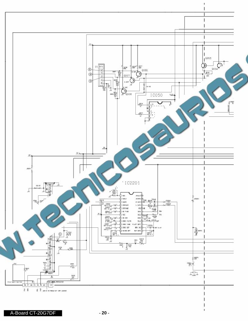
- 20 -A-Board CT-20G7DF
- 21 - A-Board CT-20G7DF
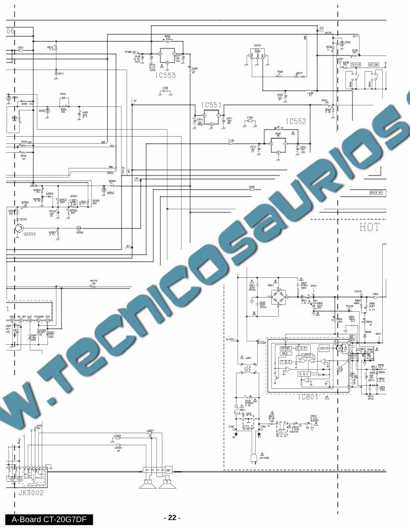
- 22 -A-Board CT-20G7DF
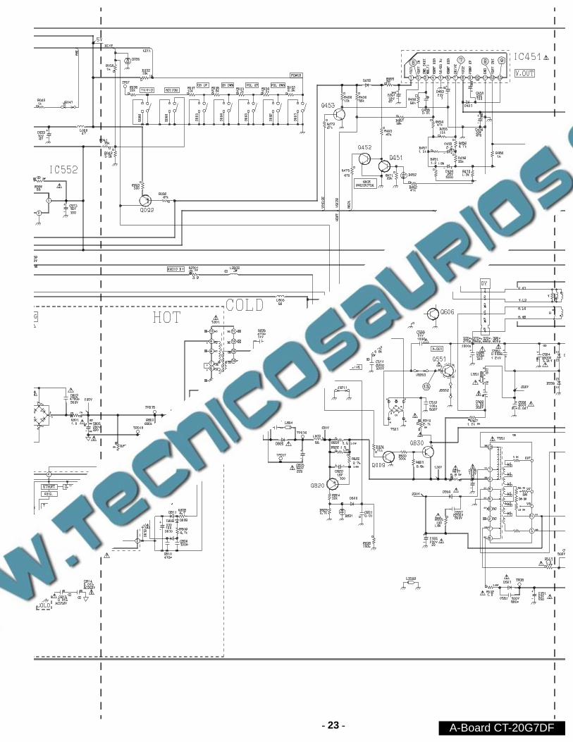
- 23 - A-Board CT-20G7DF
- 24 -A-Board CT-20G7DF
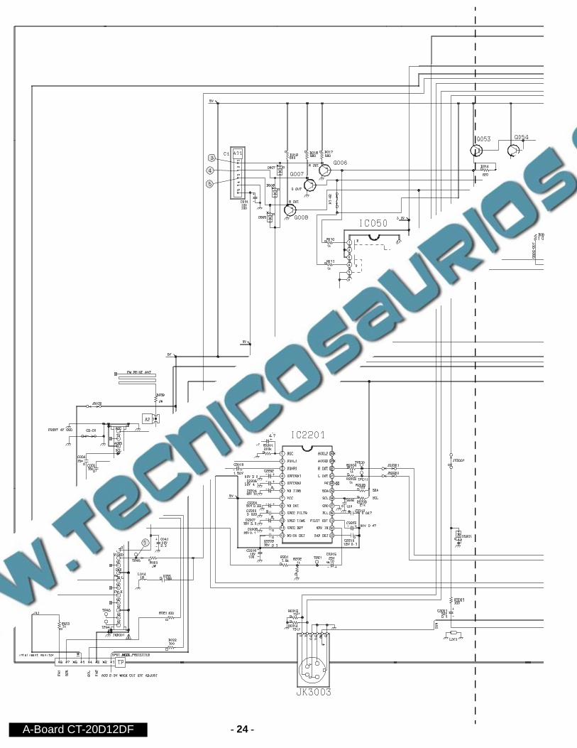
- 24 -A-Board CT-20D12DF
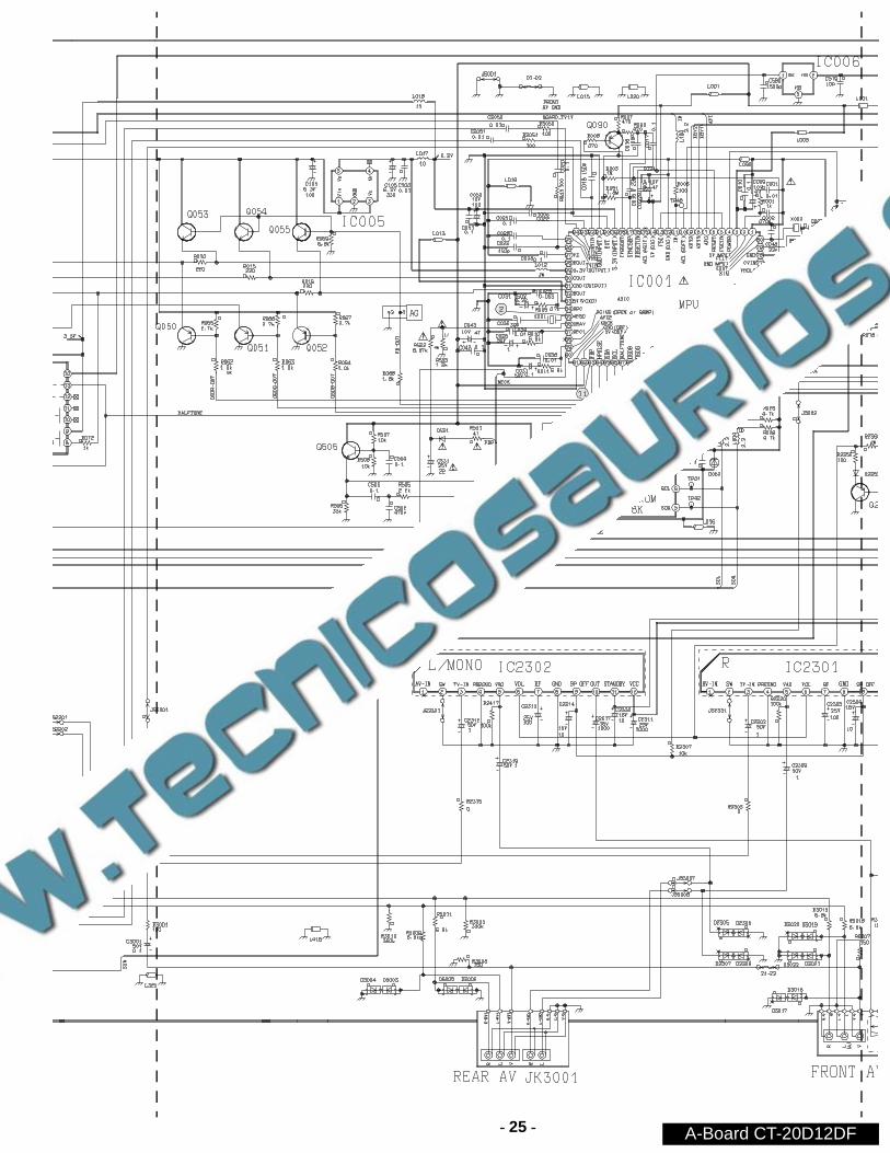
- 25 - A-Board CT-20D12DF
- 26 -A-Board CT-20D12DF
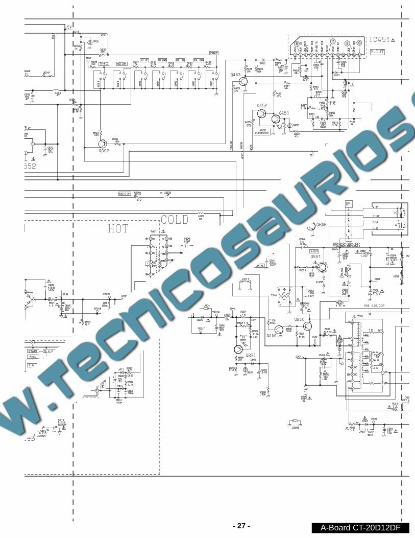
- 27 - A-Board CT-20D12DF
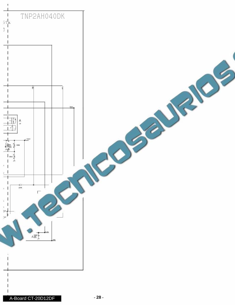
- 28 -A-Board CT-20D12DF
- 29 -
Q351
7.4796.00
7.00
Q352
7.4098.20
6.90
BCE
Q354
2.907.502.40
Q355
2.907.402.40
BCE
Q353
7.4098.80
6.90
Q356
2.907.402.40
C-Board transistor voltages
C-Board schematic
C-Board schematic & transistor voltages
- 30 -
A-Board Waveforms (All Models -- Todos los Modelos)


![Sencore Big Mack Adaprters (Making Your Own)[1]](https://static.documents.pub/doc/80x56/552c805a4a7959d27c8b4731/sencore-big-mack-adaprters-making-your-own1.jpg)

