Introduction OLEDs OTFTs OPVC Summary Organic Electronics Felix Buth Walter Schottky Institut, TU München Joint Advanced Student School 2008 Organic Electronics Walter Schottky Institut, TU München
Transcript
Introduction OLEDs OTFTs OPVC Summary
Organic Electronics
Felix Buth
Walter Schottky Institut, TU München
Joint Advanced Student School 2008
Organic Electronics Walter Schottky Institut, TU München
Introduction OLEDs OTFTs OPVC Summary
Outline1 Introduction
Difference organic/inorganic semiconductorsFrom molecular orbitals to the molecular crystal
Dark spots on a ITO/α-NPD/Alq3/Al OLED from: Kim et al.
Appl. Phys. Lett. 89, 132108 (2006)
Organic Electronics Walter Schottky Institut, TU München
Introduction OLEDs OTFTs OPVC Summary
Electrical Properties
Molecular Orbitals
Interaction between the atomic orbitals leads to bonding andanti-bonding molecular orbitalsSplitting determined by the interaction between the atoms
Organic Electronics Walter Schottky Institut, TU München
Introduction OLEDs OTFTs OPVC Summary
Electrical Properties
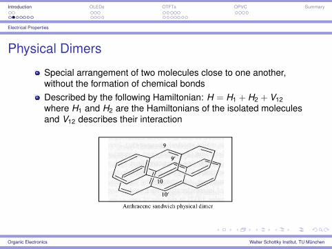
Physical Dimers
Special arrangement of two molecules close to one another,without the formation of chemical bondsDescribed by the following Hamiltonian: H = H1 + H2 + V12where H1 and H2 are the Hamiltonians of the isolated moleculesand V12 describes their interaction
Organic Electronics Walter Schottky Institut, TU München
Introduction OLEDs OTFTs OPVC Summary
Electrical Properties
Ground States of a Physical Dimer
Approximation of the ground state wavefunction as the product of thetwo molecular states:
Dimer Ground StateΨg = Ψ1Ψ2
The resulting energy of the ground state is the sum of the twomolecular states, but shifted by the coulombic binding energy W :
Organic Electronics Walter Schottky Institut, TU München
Introduction OLEDs OTFTs OPVC Summary
Basic Principals
Organic Light Emitting Diodes (OLEDs)
Principal of OLEDs first demonstrated in 1963 by Pope inanthraceneFirst comparably efficient OLED by Tang and van Slyke in 1987using Alq3
Organic Electronics Walter Schottky Institut, TU München
Introduction OLEDs OTFTs OPVC Summary
Basic Principals
Charge Carrier Injection
from N.Koch, ChemPhysChem 2007, 8, 1438 – 1455
Charge carriers need to overcome a potential barrier in order to getinto the semiconductor→ Metal with high workfunction (Φ1) for hole injection and one withlow workfunction (Φ2) for electron injection
Organic Electronics Walter Schottky Institut, TU München
Introduction OLEDs OTFTs OPVC Summary
Basic Principals
Level Alignment of some Organic Materials and Metals
Organic Electronics Walter Schottky Institut, TU München
Introduction OLEDs OTFTs OPVC Summary
Multilayer OLEDs
Multilayer OLEDs
Hole and electron transferlayers to decrease the injectionbarriers
Tranparent anode needed(here: ITO)
Figures from N.Koch, ChemPhysChem 2007, 8, 1438 – 1455
Organic Electronics Walter Schottky Institut, TU München
Introduction OLEDs OTFTs OPVC Summary
Multilayer OLEDs
Exciton RecombinationFluorescence vs. Phosphorescence
fast process ≈ 1ns relatively slow process > 1ns
Organic Electronics Walter Schottky Institut, TU München
Introduction OLEDs OTFTs OPVC Summary
Multilayer OLEDs
White Organic Light Emitting Diodes
from Sun et al., NATURE 2006, Vol 440, 908-912
Use of triplet excitons for non-blue light emission
Organic Electronics Walter Schottky Institut, TU München
Introduction OLEDs OTFTs OPVC Summary
Multilayer OLEDs
OLED Performance
from Shaw and Seidler,"Organic Electronics: Introduction", IBM J. RES. & DEV.,Vol. 45
Organic Electronics Walter Schottky Institut, TU München
Introduction OLEDs OTFTs OPVC Summary
OTFT Structure
Organic Thin Film Transistors
Possible use in active matrix flat panel displays, "electronicpaper" displays, sensors or radio-frequency identification (RFID)tagsIn competition with a:Si:H which is normally used in active matrixdisplays
Organic Electronics Walter Schottky Institut, TU München
Introduction OLEDs OTFTs OPVC Summary
OTFT Structure
OTFT Structure
Low conductivity in thechannel without any gatevoltageFormation of positive(negative) accumulationlayer at thesemiconductor-insulatorinterface upon applicationof a negative (positive) gatevoltageHigh crystallinity needed toobtain high mobilities→use of SAMs
Organic Electronics Walter Schottky Institut, TU München
Introduction OLEDs OTFTs OPVC Summary
OTFT Structure
Typical Transistor Characteristic
Organic Electronics Walter Schottky Institut, TU München
Introduction OLEDs OTFTs OPVC Summary
OTFT Structure
Combining OLED and OTFT
The Organic Light Emitting Transistor
from
Muccini, nature materials, Vol. 5 (2006), p. 605-613
Useful for example in activematrix displays. No separateOLEDs and OTFTS needed→thinner and less complicatedarrangement
Organic Electronics Walter Schottky Institut, TU München
Introduction OLEDs OTFTs OPVC Summary
OTFT Structure
Charge Carrier Mobility
Mobility measurable with the help of TFTs: IDS,sat = W2L Cµ (VG − VT )2
Hole mobilityElectron mobility
Three orders of magnitude lower than in inorganic semiconductors
Organic Electronics Walter Schottky Institut, TU München
Introduction OLEDs OTFTs OPVC Summary
Transport in organic semiconductors
Why is the mobility so low?Weak inter-molecular coupling leads to high effective massAmorphous material→ thermally activated hopping transport, noband transportPolycrystalline material→ scattering at grain boundaries"Self-trapping" of charge carriers - the polaron
Organic Electronics Walter Schottky Institut, TU München
Introduction OLEDs OTFTs OPVC Summary
Transport in organic semiconductors
Hopping TransportIn amorphous solids (also a-Si:H) the charge carriers are highlylocalised due to disorderPhonon assisted transport→ mobility increases with risingtemperature µ ∝ exp(−E/kT )
Organic Electronics Walter Schottky Institut, TU München
Introduction OLEDs OTFTs OPVC Summary
Transport in organic semiconductors
Polycrystalline Pentacene
When diffusing from one grainto another, charge carriers getscattered at the defectsintroduced by the grainboundaries. These boundarieshence reduce the effectivemobility.
Organic Electronics Walter Schottky Institut, TU München
Introduction OLEDs OTFTs OPVC Summary
Transport in organic semiconductors
The Polaron in Ionic Materials
Rearrangement of the latticeunder the influence of the electricfield of the charge carrierResulting potential well hindersthe motion of the charge, thusreducing its mobility
Organic Electronics Walter Schottky Institut, TU München
Introduction OLEDs OTFTs OPVC Summary
Transport in organic semiconductors
Polarons in π-conjugated Polymers
Polymer rearranges itself in the presence of a charge carrier(here a hole), in order to be in the state of lowest energy.This configuration change goes in hand with a lattice distortion.
Organic Electronics Walter Schottky Institut, TU München
Introduction OLEDs OTFTs OPVC Summary
Transport in organic semiconductors
Polaron Transport
In order to move the charge carrier the deformation needs tomove too→ low mobility of the polaron.Presence of phonons is increasing the mobility of the polaron.
Organic Electronics Walter Schottky Institut, TU München
Introduction OLEDs OTFTs OPVC Summary
Transport in organic semiconductors
Polaron-Excitons in OLEDs
Injection of positively and negatively charged polarons at theelectrodes.Migration of the polarons in the external field.When the two oppositely charged polarons meet they form apolaron-exciton, which can eventually recombine.
Organic Electronics Walter Schottky Institut, TU München
Introduction OLEDs OTFTs OPVC Summary
Differences to inorganic solar cells
Organic Photovoltaic CellsPhotovoltaic effect in single layer organic molecules firstobserved in the 1970s, later on also for polymersCells consisting of a single material reach only very lowefficiencies→ combination of at least two materials necessary
Organic Electronics Walter Schottky Institut, TU München
Introduction OLEDs OTFTs OPVC Summary
Differences to inorganic solar cells
Why two dissimilar materials?
Photon absorption leads to the formation of a neutral exciton,which is stable at room temperatureExciton dissociation is increased at organic-organic interfaceswith proper band alignment
Organic Electronics Walter Schottky Institut, TU München
Introduction OLEDs OTFTs OPVC Summary
Differences to inorganic solar cells
Operation Principle of OPVCs
Exciton formation by absorptionof a photonDiffusion of the neutral exciton tothe organic-organic interface(diffusion length up to a few tensof nanometers)Dissociation of the exciton at theinterfaceCollection of the charge carriersat the electrodes
Organic Electronics Walter Schottky Institut, TU München
Introduction OLEDs OTFTs OPVC Summary
Differences to inorganic solar cells
OPVC Performance
Organic Electronics Walter Schottky Institut, TU München
Introduction OLEDs OTFTs OPVC Summary
Summary
Organic semiconductors offer a low cost alternative toestablished semiconductors when it comes to large area and lowcost applicationsFirst OLED applications are already on the market. OTFTs andOPVCs will most probably follow.Improvements on the material side are still needed (e.g. bettersolubility of small molecular crystals or doping possibilities)
Organic Electronics Walter Schottky Institut, TU München