Organic Photovoltaics Based on Solution Cast Polymers and Boron Subphthalocyanines – Hybrid Device
Architectures Enabling Novel Material Combinations
by
Stephanie Robin Nyikos
A thesis submitted in conformity with the requirements for the degree of Master of Applied Science
Department of Chemical Engineering and Applied Chemistry University of Toronto
© Copyright by Stephanie Robin Nyikos 2018
ii
Polymer/BsubPc Organic Photovoltaics – Hybrid Device
Architectures Enabling Novel Material Combinations
Stephanie Robin Nyikos
Master of Applied Science
Department of Chemical Engineering and Applied Chemistry
University of Toronto
2018
Abstract
Solution-cast films of crystalline electron donating poly(3,3”’-didodecylquaterthiophene) (PQT-
12) were studied in pseudo-planar heterojunction (PPHJ) organic photovoltaic devices (OPVs)
paired with boron subphthalocyanine (BsubPc) as the electron acceptor layer, and the effects of
crystallinity domain size and layer thickness were investigated. Annealed, 10-20 nm films of
intermediate-sized crystals were 40% more efficient than un-annealed PQT-12 layers and had
comparable efficiency to their fullerene-based BHJ counterparts, demonstrating the ability of
polymer|BsubPc PPHJ OPVs to accommodate highly crystalline polymers with a tendency to
phase segregate and create devices with favorable electrical properties. These polymer|BsubPc
PPHJs were further studied with the new amorphous copolymer electron donating material
PBTZT-stat-BDTT-8. While optimized PPHJ devices of PBTZT-stat-BDTT-8|BsubPc had
substantially lower efficiency than PBTZT-stat-BDTT-8|fullerene BHJs (which were free of
morphological problems), they demonstrated comparable performance to their BHJ equivalents
due to ideal morphology, presenting a pathway forward for OPV design of otherwise phase
segregating polymer|BsubPc pairings.
iii
Acknowledgments
I would like to extend my utmost gratitude to my supervisor, Prof. Tim Bender, for his guidance
and support which helped navigate me through the course of my research. Thank you greatly for
your encouragement and direction.
I would also like to thank all my colleagues in the Bender lab for their optimism and excellent
advice. They challenged me to participate more in departmental groups and events, which added
amazing depth to my graduate school experience.
Lastly, my heartfelt thanks to my family and friends for their continued love and support, for
believing in me and pushing me to be my very best.
iv
Table of Contents
Acknowledgments......................................................................................................................... iii
Table of Contents ........................................................................................................................... iv
List of Tables ................................................................................................................................ vii
List of Figures .............................................................................................................................. viii
List of Appendices ......................................................................................................................... xi
Chapter 1 ....................................................................................................................................... xii
Introduction .................................................................................................................................1
1.1 Motivation ............................................................................................................................1
1.2 Background ..........................................................................................................................2
1.2.1 Brief Overview of OPV Development .....................................................................2
1.2.2 Device Physics .........................................................................................................3
1.2.3 Performance Metrics and J-V Curves ......................................................................6
1.2.4 Device Architecture .................................................................................................8
1.3 Outline................................................................................................................................14
Chapter 2 ........................................................................................................................................15
Materials and Methods ..............................................................................................................15
2.1 Materials ............................................................................................................................15
2.1.1 PEDOT:PSS ...........................................................................................................16
2.1.2 BCP ........................................................................................................................16
2.1.3 Silver ......................................................................................................................17
2.1.4 BsubPc ...................................................................................................................17
2.2 Experimental Methods .......................................................................................................18
2.2.1 Substrate Preparation and Cleaning .......................................................................18
2.2.2 Profilometry ...........................................................................................................20
2.2.3 Physical Vapor Deposition ....................................................................................21
v
2.2.4 OPV Light Testing .................................................................................................22
Nano-crystalline poly(3,3”-didodecyl-quarterthiophene) in pseudo-Planar Heterojunction
Organic Photovoltaics ...............................................................................................................25
3.1 Introduction ........................................................................................................................25
3.2 PQT-12 Thermal Transition Analysis ................................................................................28
3.3 Analysis of Solution Processed Films................................................................................29
3.3.1 Spin-coated Film Profilometry ..............................................................................29
3.3.2 Atomic Force Microscopy of PQT-12 Films .........................................................29
3.3.3 Ultraviolet-Visible Spectroscopy of PQT-12 Films ..............................................31
3.4 Performance in Organic Photovoltaic Devices ..................................................................32
3.4.1 PQT-12 OPV Performance with Cl-BsubPc ..........................................................32
3.4.2 Comparison of PQT-12, P3HT, and α6T OPVs ....................................................36
3.5 Chapter Conclusion ............................................................................................................39
PBTZT-stat-BDTT-8 in pseudo-Planar Heterojunction Organic Photovoltaics .......................40
4.1 Introduction ........................................................................................................................40
4.2 PBTZT-stat-BDTT-8 Film Profilometry ...........................................................................44
4.3 Performance and Optimization of OPVs based on PBTZT-stat-BDTT-8/Cl-BsubPc.......44
4.4 PBTZT-stat-BDTT-8 in “Cnops Stack”.............................................................................48
4.5 OPV Comparison of BsubPc Electron Acceptor Layers with PBTZT-stat-BDTT-8 ........50
4.5.1 Overcoming Replication Issues .............................................................................52
4.6 PBTZT-stat-BDTT-8 in Cl-Cl6BsubPc and PhO-Cl6BsubPc OPVs – BHJ vs PPHJ
Architecture........................................................................................................................54
4.7 Chapter Conclusion ............................................................................................................57
Summary and Future Work .......................................................................................................58
5.1 Summary ............................................................................................................................58
5.2 Future Work .......................................................................................................................60
References ......................................................................................................................................62
vi
Appendices .....................................................................................................................................69
Appendix A ...............................................................................................................................69
vii
List of Tables
Table 1.1 | Summary of literature PPHJ Photovoltaic Device Performance ................................ 13
Table 3.1 | Summary of literature PQT-12/fullerene BHJ performance ....................................... 26
Table 3.2 | Characteristic device parameter comparison of P3HT, PQT-12, and α6T donor layers
paired with Cl-BsubPc. ................................................................................................................. 37
Table 4.1 | Characteristic parameters of PBTZT-stat-BDTT-8/Cl-BsubPc devices. The layer
thickness of Cl-BsubPc was constant at 20 nm. ........................................................................... 46
Table 4.2 | Characteristic parameters of OPV devices with varying electron acceptor layer. The
layer thickness of PBTZT-stat-BDTT-8 was constant at 20 nm................................................... 49
Table 4.3 | Characteristic parameters of PBTZT-stat-BDTT-8/BsubPc devices with a 10 nm
electron acceptor layer. ................................................................................................................. 51
Table 4.4 | Characteristic parameters of PBTZT-stat-BDTT-8/BsubPc devices with a 20 nm
electron acceptor layer. ................................................................................................................. 52
Table 4.5 | Characteristic parameters of PBTZT-stat-BDTT-8/BsubPc devices in either pseudo-
Planar Heterojunction or Bulk Heterojunction architectures. ....................................................... 55
viii
List of Figures
Figure 1.1| Electronic Structure of an OPV. ................................................................................... 3
Figure 1.2 | Stack Architecture of a PHJ OPV. ............................................................................... 3
Figure 1.3 | Left: Solar testing J-V curve and Right: EQE results of a a6T/Cl-BsubPc planar
heterojunction baseline device under simulated solar illumination. The shaded area in both
graphs represent one standard deviation from the average. Important device testing parameters
used to calculate total device efficiency are marked. ..................................................................... 7
Figure 1.4| Pictorial representation of a) Bulk Heterojunction (BHJ) b) Planar Heterojunction
(PHJ) and c) Pseudo-Planar Heterojunction (PPHJ) OPV Architectures. ...................................... 8
Figure 1.5 | Device performance of PTB7/PCBM bilayer diffusion devices annealed at 150°C for
varying times. Device JSC is maximized after 10 min of annealing, resulting in the highest device
PCE. Reproduced with permission from ref. 42, Advanced Energy Materials 2013. .................. 11
Figure 1.6 | A comparison of the photovoltaic performance of devices based on traditional BHJ
PTB7:PCBM films (PCE = 5.9%) and sequentially-processed films with the fullerene layer cast
from a 50:50 2-CP:1-butanol co-solvent blend (PCE = 6.0%). Reproduced from ref. 43,
Advanced Energy Materials 2015. ................................................................................................ 12
Figure 1.7 | Cross-sectional TEM image showing incomplete mixing of C70/PBDTTT-C-T to
form a diffusive quasi-bilayer structure. Reproduced from ref. 44, Journal of Materials
Chemistry A 2014. ......................................................................................................................... 12
Figure 2.1 | Molecular structure of a) PEDOT:PSS b) BCP c) Cl-BsubPc d) P3HT and e) α6T. 15
Figure 2.2 | Glass/ITO Substrate Cleaning Procedure. ................................................................. 18
Figure 2.3 | The nitrogen glovebox (MARI) and vacuum chamber (KATE) setup used to
fabricate and test all OPVs for this thesis. .................................................................................... 21
Figure 2.4 | Custom-built substrate holders for light testing......................................................... 22
ix
Figure 3.1 | a) Chemical structures of poly(3-hexylthiophene-2,5-diyl) (P3HT), poly(3,3’’’–
didodecyl-quaterthiophene) (PQT-12), and chloro-boron subphthalocyanine (Cl-BsubPc) and b)
their reported frontier molecular orbital energy levels. c) Device schematic in which the electron
donor layer is varied with all other layers held constant. ............................................................. 26
Figure 3.2 | Left: TGA data and Right: DSC thermogram of PQT-12. Film annealing
temperatures are marked. .............................................................................................................. 28
Figure 3.3 | Profilometry results of PQT-12 on Glass/ITO/PEDOT:PSS substrates. ................... 29
Figure 3.4 | Tapping mode AFM images of 55 nm thick films of PQT-12. On the left are
topographic images, while images on the right are phase. ........................................................... 30
Figure 3.5 | UV/Vis absorption coefficient spectra of 55 ± 5 nm thick films of PQT-12. ........... 32
Figure 3.6 | Left: J-V characteristics and Right: EQE spectra of OPV devices optimized around
the electron donor layer thickness. The PQT-12 layer was prepared a) unannealed and annealed
at b) 118 °C c) 133 °C and d) 148 °C, paired with Cl-BsubPc. Shading indicates one standard
deviation from the average. ........................................................................................................... 34
Figure 3.7 | Plotted characteristic parameters of OPV devices optimized around the electron
donor layer thickness. ................................................................................................................... 35
Figure 3.8 | Comparison of the Left: J-V characteristics and Right: EQE spectra of P3HT, PQT-
12, and α6T electron donor layers paired with Cl-BsubPc. Shading indicates one standard
deviation from the average. ........................................................................................................... 37
Figure 4.1 | Chemical structures of a) BsubPc electron acceptor molecules and b) polymeric
electron donor materials, with c) their reported frontier orbital molecular energy levels. d)
Device schematic of pseudo-PHJ devices in which the BsubPc is varied. ................................... 41
Figure 4.2 | Profilometry results of PBTZT-stat-BDTT-8 on Glass/ITO/PEDOT:PSS substrates.
....................................................................................................................................................... 44
x
Figure 4.3 | Left: J-V curves and Right: EQE spectra of PBTZT-stat-BDTT-8/Cl-BsubPc devices
with varying electron donor layer thickness, constant 20 nm electron acceptor layer thickness.
Shaded error bars represent ±1 standard deviation from the mean. .............................................. 46
Figure 4.4 | Characteristic parameters of PBTZT-stat-BDTT-8/Cl-BsubPc devices, visualized to
display trends with increasing thickness. ...................................................................................... 47
Figure 4.5 | Left: J-V curves and Right: EQE spectra of OPV devices with varying electron
acceptor layer and constant 20 nm PBTZT-stat-BDTT-8 electron donor layer. Shaded error bars
represent ±1 standard deviation from the mean. ........................................................................... 49
Figure 4.6 | Left: J-V characteristics and Right: EQE spectra of OPV devices containing PBTZT-
stat-BDTT-8 as the electron donor layer and Cl-BsubPc, Cl-Cl6BsubPc, or PhO-Cl6BsubPc as
electron acceptor layer. Shaded error bars represent ±1 standard deviation from the average..... 51
Figure 4.7 | Comparison of VOC and FF of pseudo-Planar Heterojunction or Bulk Heterojunction
architectures. ................................................................................................................................. 55
Figure 4.8 | Comparison of the Left: J-V characteristics and Right: EQE spectra of PBTZT-stat-
BDTT-8/BsubPc OPVs in either pseudo-Planar Heterojunction or Bulk Heterojunction
architectures. Shaded error bars represent ± 1 standard deviation from the average.................... 55
xi
List of Appendices
A-1 | Replication testing of PPHJ OPVs with PBTZT-stat-BDTT-8 (30 nm)/Cl-Cl6BsubPc (10
nm)
A-2 | Replication testing of PPHJ OPVs with PBTZT-stat-BDTT-8 (60 nm)/Cl-Cl6BsubPc (10
nm)
A-3 | Replication testing of PPHJ OPVs with PBTZT-stat-BDTT-8 (30 nm)/Cl-Cl6BsubPc (20
nm)
A-4 | Replication testing of PPHJ OPVs with PBTZT-stat-BDTT-8 (60 nm)/Cl-Cl6BsubPc (20
nm)
xii
List of Abbreviations
α6T α-sexithiophene
AFM Atomic force microscopy
AIBN 2,2’-azobis(isobutyronitrile)
BCP Bathocuproine
BDT Benzodithiophene
BHJ Bulk heterojunction
BsubPc Boron subphthalocyanine
BT Benzothiadiazole
Cl-BsubPc Chloro-boron subphthalocyanine
Cl-Cl6BsubPc Chloro hexachloro-boron subphthalocyanine
D-A Donor-Acceptor
DCB 1,2-dichlorobenzene
DIO 1,8-diiodooctane
DSC Differential scanning calorimetry
EQE External quantum efficiency
FF Fill factor
GIWAXS Grazing-incidence wide-angle X-ray scattering
HOMO Highest occupied molecular orbital
ITO Indium tin oxide
J Current density
JSC Closed circuit current
LUMO Lowest unoccupied molecular orbital
OFET Organic field effect transistor
OPV Organic photovoltaic device
OTFT Organic thin film transistor
Pin Incident light intensity
P3HT poly(3-hexylthiophene-2,5-diyl)
PCBM 1-(3-methoxycarbonyl)-propyl-1-phenyl-[6,6]C61
PCE Power conversion efficiency
PEDOT:PSS poly(3,4-ethylenedioxythiophene) poly(styrene-sulfonate)
PHJ Planar heterojunction
xiii
PhO-Cl6BsubPc Phenoxy hexachloro-boron subphthalocyanine
PPHJ Pseudo planar heterojunction
PQT-12 poly(3,3”’ -didodecylquaterthiophene)
PTB7 poly[[4,8-bis[(2-ethylhexyl)oxy]benzo[1,2-b:4,5-b']dithiophene-2,6-
diyl][3-fluoro-2-[(2-ethylhexyl)carbonyl]thieno[3,4-b]thiophenediyl]]
PVD Physical vapor deposition
SubNc Chloro-boron subnaphthalocyanine
TGA Thermo-gravimetric analysis
TT Thieno[3,4-b]thiophene
UV-vis Ultraviolet-visible spectroscopy
V Voltage
VOC Open circuit voltage
1
Chapter 1
Introduction
Introduction
1.1 Motivation
The world’s growing demands in energy consumption, combined with harmful emissions released
through the exploitation of inexpensive yet environmentally damaging energy sources such as
fossil fuels, has brought the issue of climate change to the forefront of public discussion. With
programs coming online to incentivize zero emission energy generation, as well as the roll out of
modern electrical metering infrastructure allowing all homeowners to generate and potentially sell
their own electricity, there is a clear public desire for small scale sustainable energy generation.1,
2 Solar energy is the fastest growing source of green energy for small-scale generation due to its
modular design and rapidly decreasing price per kWh.2 However, traditional silicon solar
technology suffers from numerous constraints which limit its application. The cells are heavy and
brittle, necessitating the installation of potentially extensive supporting infrastructure which drives
up system cost. This requirement limits traditional solar cells to the tops of roofs or a flat open
backyard, which is not always feasible. Furthermore, traditional solar cells are fabricated using a
single slab of high-purity silicon in an expensive, energy-intensive process which keeps initial
capital costs high compared to other methods of generating electricity.
Organic photovoltaics (OPVs) have attracted significant attention in recent years due to their
potential as lightweight, low-cost, flexible solar cells.3, 4 While OPVs are not necessarily a
replacement for silicon cells due to their comparatively low power conversion efficiencies (PCEs),
their strength lies in the sheer number of potential commercial applications for a mass-producible,
lightweight, fully flexible solar cell. These semi-transparent solar cells can be roll-to-roll printed
onto sheets of plastic and employed practically anywhere with little or no supporting infrastructure
required.5, 6 For example, they could be installed on building façades to help meet inhabitant’s
electricity requirements or installed on the top and sides of electric vehicles to improve their
efficiency. Unlike silicon-based cells, OPVs retain their efficiency at low light levels, allowing
them to output energy in the shade or on a cloudy day.7-10 Despite OPVs numerous benefits, these
cells have only ever been installed for small-scale projects; larger scale commercialization has yet
2
to be achieved. While significant progress has been made towards improving the PCE and lifetime
of OPVs, further work must be done for this technology to truly flourish outside of a lab
environment.
One promising avenue of research towards this goal is the optimization of material choice within
the photoactive stack. OPVs require two types of photoactive material to function: an electron
donor layer and an electron acceptor layer. These layers have traditionally been deposited either
entirely from solution, or entirely from physical vapor deposition. Insoluble materials cannot be
solution deposited, and heavy polymers cannot be vapor deposited. This limitation has restricted
the combinations of electron donor/acceptor layers available with which to fabricate solar cells.
Overcoming this limitation opens the door for novel material combinations and solar device
architectures between polymers and small molecules, which may lead to improvements in OPV
efficiency and lifetime.
1.2 Background
1.2.1 Brief Overview of OPV Development
Historically, the discovery of photoconductivity in solid anthracene in 1906 marked the beginning
of the field of organic photovoltaics.11 Early investigations into OPV devices came in the 1950s
with the study of organic dyes such as chlorophyll and continued with studies into semiconducting
polymers. Efficiencies from these early single-junction devices were very low, under 0.1%. A
major breakthrough in the field came in 1986 when Tang reported the first bilayer device which
achieved and efficiency of 1%.12 In the paper, Tang first proposed the operating principle of the
electron donor/acceptor interface which is still accepted today. In 1993, Sariciftci et al. reported
the first polymer/C60 device, which achieved an efficiency of 0.04%.13 They outlined a method of
spin-coating the polymeric electron donor layer and vapor depositing the insoluble C60 layer in a
very similar technique to that used in this thesis to incorporate polymers and insoluble small
molecules in the same device. In 1995, Yu et al. reported polymer/fullerene blend OPVs which
were the first example of bulk heterojunction (BHJ) devices.14 The long interface of the electron
donor/acceptor layers was shown to improve device photogeneration and current density. Since
then, OPV technology has shown steady development in PCEs driven by molecular design of
3
photovoltaic molecules and improvements in device engineering. Record breaking efficiencies of
13% have recently been reported and certified for state-of-the-art fullerene-free BHJ devices with
a polymeric electron donor and small-molecule electron acceptor.15 The record for the highest
efficiency OPV is frequently broken, driven by significant research efforts to develop novel high-
performance semiconducting materials. While there are some caveats to these efficient OPVs, such
as difficult material synthesis and untested working cell lifetimes, the future of OPVs remains very
bright.
1.2.2 Device Physics
All OPV devices are composed of stacked layers of materials where each layer is
exceptionally thin, typically 1-200 nm for planar heterojunction solar cells (PHJs). Figure 1.1
Figure 1.2 | Stack Architecture of a PHJ OPV.
1. Light enters the device through the transparent
anode/hole transport layer and is absorbed by
chromophores in the two photoactive materials.
2. Excited materials produce excitons which
migrate to the electron donor/acceptor interface.
3. Excitons dissociate at the interface into electrons
and holes.
4. Charge carriers migrate to their respective
electrodes to produce current
Figure 1.1| Electronic Structure of an OPV.
1. Exciton dissociation at the electron
donor/acceptor interface is driven by the energy
difference between the HOMO of the donor and
the LUMO of the acceptor material. This energy
is approximately equal to the device’s Voc.
2. Holes travel along the HOMO of the donor
and electrons travel along the LUMO of the
acceptor towards their respective electrode.
3. Charge carriers jump across interface to their
respective electrode, a process facilitated by
electron/hole transport layers (not shown).
4
depicts the standard layer design of a PHJ OPV stack, while Figure 1.2 depicts its electronic
structure.
1.2.2.1 Light Absorption
The electron donor and acceptor layers are composed of semiconducting organic molecules which
strongly absorb visible wavelength light. Their conductive and photoactive properties are a result
of conjugated systems formed from multiple covalently bonded carbon atoms with adjacent p-
orbitals. The p-orbitals overlap and connect to from a bonding π-orbital and antibonding π*-orbital,
allowing π-electrons to delocalize across the system in order to reduce the free energy of the system
and increasing stability. Conjugated systems are depicted as alternating double and single bonds,
but the π-electrons belong to the group of atoms rather than any specific bond. The energy level
of the π-orbital is known as the highest occupied molecular orbital (HOMO) which is analogous
to the valence band of an inorganic semiconductor, while the energy level of the π*-orbital is
known as the lowest unoccupied molecular level (LUMO) and is analogous to a conduction band.
The band gap of an organic semiconductor is the energy separation between its HOMO and LUMO
levels. The width and depth of the bandgap is a critical factor in the molecular design of organic
photoactive materials. Organic semiconductors may only absorb photons with energy greater than
the band gap. For example, if the width of a material’s band gap is 2.5 eV, it can only absorb
green/blue light with photon energies of 2.5 eV or higher. Light with lower photons energies, such
as yellow and red light, will pass straight through the material as if it were transparent. Light with
much higher photon energies, such as purple and ultraviolet light, may still be absorbed, but energy
in excess of the bandgap is released as heat which can be detrimental to device performance.
1.2.2.2 Exciton Transport and Dissociation
Upon absorbing photons, a region of the conjugated system becomes excited and forms a
Coulombically bound electron-hole pair called an exciton.16 Excitons have no net electrical charge
and may transport energy through the material via diffusion away from areas with a high exciton
concentration. The diffusion length of excitons is limited to about ~15 nm because of their
relatively short lifetime, after which they decay back to their ground state.17 In organic
semiconductors, the aim is for excitons to diffuse to the electron donor/acceptor interface before
they decay.18 The energy difference between the HOMO of the electron donor layer and the LUMO
of the electron acceptor layer must be sufficient to overcome the exciton binding energy (typically
5
0.25-1 eV in organic materials)19 to dissociate a free electron and electron hole. The efficiency of
exciton dissociation is dependent on the area of the interface, the lifetime of the exciton, and its
ability to diffuse to the interface within that lifetime.20 The dissociated electrons and holes
experience significant coulombic attraction across the interface and may recombine if not
separated quickly.21 However, the competing coulombic repulsion of many like-charged electrons
and holes at the interface drive the newly dissociated charge carriers away from one another.
1.2.2.3 Charge Transport
Once dissociated, electrons travel through the electron acceptor layer to the metal cathode and
holes travel through the electron donor layer to the transparent anode. Charge carrier
recombination occurs when free electrons meet with free holes. The charge carrier mobility of the
photoactive layers must be approximately equal to ensure charge traverses through the layers at
approximately the same rate. Charge carrier mobility imbalance, as well as high interfacial energy
barriers between the electron donor/acceptor layers has been known to cause charge accumulation
in which charges cannot exit the device at an appreciable rate. Charge build-up at interfaces can
give rise to ‘S-kinks’, s-shaped current-voltage curves which greatly lowers OPV fill factor (FF)
and decreases performance.22, 23 Choice of layer material and transport layer crystallinity are
crucial to avoid charge accumulation issues.
1.2.2.4 Charge Extraction
After traversing the photoactive materials, charge carriers travel through a transport layer to reach
their respective electrode where they can be extracted to yield a photocurrent. These interface
buffer layers serve four important functions which significantly improve device performance.
Firstly, they block any stray opposite sign charge carriers from reaching the electrodes and
reducing the photocurrent. To do this, the material must have a high energy barrier for opposite
sign charges to jump across the layer interface based on their energy level alignment. Secondly,
interface buffer layers act as both diffusion barriers between the metal electrode and photoactive
layer, reducing the number of defects and recombination sites caused by metal penetration into the
photoactive layer. In doing so, they prevent any metal/organic chemical reactions from taking
place and degrading the layer materials. Thirdly, they improve the energy level alignment of the
metal/organic interface by changing the metal’s effective work function. This lowers the energy
barrier for charge carriers to traverse the electrode interface. Finally, interfacial buffer layers
6
protect the photoactive material from damage during electrode deposition, reducing the number of
defects introduced during device fabrication. In this thesis, bathocuproine (BCP) is used as the
electron transport layer and PEDOT:PSS is used as the hole transport layer. Both are well-studied
and commonly used transport layers which are known to significantly improve device
performance24-27 and will be further discussed in the next section.
In this thesis, the OPV cathode layer is an 80nm thick layer of Ag. Ag has a work function which
matches the energy levels of BCP, allowing electrons to easily make their way across the material
interface.27 It forms smooth, even films when vapor deposited, and is easier to deposit than other
commonly used cathode materials such as Al. The cell anode is a 120nm thick layer of indium tin
oxide (ITO) on top of a structurally supportive glass substrate. ITO is a conductive metal oxide
whose work function matches the energy levels of PEDOT:PSS. Critically, it is also transparent to
allow light into the OPV where it may be absorbed by the photoactive layers.28
1.2.3 Performance Metrics and J-V Curves
The performance of OPV devices can be quantified into three important characterization
parameters: open circuit voltage (VOC), short circuit current (JSC), and fill factor (FF). The OPV’s
power conversion efficiency (PCE) is defined as the fraction of incident power that is converted
into electricity, and may be calculated using these three numbers along with the incident light
intensity (Pin) by the following relationship:
PCE =VOC JSC FF
Pin
7
These metrics are determined through solar testing, which is further discussed in the methods
section of this thesis. Figure 1.4 displays typical graphs generated from solar testing data. As
previously discussed, the VOC can be approximated by the LUMO energy of the electron acceptor
and the HOMO level of the electron donor. Additionally, the VOC is heavily influenced by the
amount of charge carrier recombination that occurs as dissociated charges travel to their respective
electrodes. This phenomenon is a more pressing issue for BHJ architecture devices as it is strongly
affected by phase morphology.29 Generally, a higher VOC produces a better PCE. However, to
achieve a higher VOC, there must be a larger energy difference between the two photoactive
materials which can lead to a reduction in charge dissociation across the interface, which in turn
leads to lower device JSC and FF. A careful balance must be found between VOC and the other
characteristic parameters to achieve optimal device performance.
The JSC and FF are dependent on a much larger number of factors including light intensity,
temperature,30, 31 active layer thickness,32 and film morphology.33, 34 An OPV device outputs its
maximum power at VMAX and JMAX. An OPV should be operated at its VMAX to ensure it outputs
the maximum amount of electricity. The FF indicates internal energy losses within the cell and is
graphically the ‘squareness’ of the J-V curve. FF is the ratio of the maximum power to the product
of the cell’s VOC and JSC. The ideal value for FF is 1, meaning there are no internal losses occurring
Figure 1.3 | Left: Solar testing J-V curve and Right: EQE results of a a6T/Cl-BsubPc planar
heterojunction baseline device under simulated solar illumination. The shaded area in both graphs
represent one standard deviation from the average. Important device testing parameters used to
calculate total device efficiency are marked.
8
in the cell. An exceptional fill factor for real OPVs is ~0.7, although most OPVs have FFs between
0.5-0.7. The JSC indicates the total current produced by the device when the voltage is zero. It is
the largest current that can be produced by the device; any reductions in the JSC before JMAX are
caused by resistive losses within the OPV. The device current is dependent on the photo-generation
and collection of charge carriers as described previously. For PHJ architecture devices, this is often
the main source of efficiency reduction when compared to BHJ architecture devices due to the
decreased photoactive interfacial area.
An OPV’s external quantum efficiency (EQE) is defined as the ratio of the number of charge
carriers collected by the device to the total number of incident photons. It depends on both the
OPV’s ability to absorb photons and its ability to turn those photons into current. The EQE spectra
is generated by shining monochromatic light on the device and measuring the resulting current
generation at each wavelength. Ideally, the two photoactive layers will absorb strongly at different
wavelengths to cover more of the solar spectrum.
1.2.4 Device Architecture
The three types of OPV device architectures that are studied in this thesis are depicted in Figure
1.1. The two major device architectures in the field of OPV devices are bulk heterojunctions
(BHJs) and planar heterojunctions (PHJs). In BHJs, the two photoactive materials are combined
in solution and deposited together. OPVs with this architecture cannot incorporate insoluble
photoactive materials or even two photoactive materials with different solubility due to this
solution-processing step. Electron donor/acceptor intermixing causes BHJ OPVs to have a large
b) a) c)
Figure 1.4| Pictorial representation of a) Bulk Heterojunction (BHJ) b) Planar Heterojunction (PHJ)
and c) Pseudo-Planar Heterojunction (PPHJ) OPV Architectures.
9
interfacial area, which results in raised charge generation for this type of device architecture
compared to PHJs.35, 36 However, BHJs suffer from a lack of control over film morphology and
difficulty deconvoluting performance of electron donor/acceptor materials.
What is undertaken in my thesis is the exploration of another device architecture that will
enable the combination of a solution castable polymeric material and an additional insoluble
material – both paired together in a functional OPV device – which I will refer to as a pseudo-
planar heterojunction (PPHJ) architecture. The donor layer in a PPHJ architecture is solution
deposited while the acceptor layer is vapor deposited. electron donor/acceptor layers of PHJ
devices are vapor deposited separately to create a precisely designed and controlled interface
between the two layers. This precisely controlled layer structure is optimal for investigating new
material functionality and charge transport phenomena. Since heavy polymers degrade when
heated, photoactive materials in PHJs are restricted to small-molecules.
The PPHJ device architecture has been used in the past to fabricate poly(3-hexylthiophene-2,5-
diyl) (P3HT)/C60 OPVs. P3HT is one of the most intensely studied members in the polythiophene
family of conjugated semiconducting polymers and will be discussed more in-depth later on in this
thesis. Fullerene is highly insoluble and must be vapor deposited to obtain a thin film. P3HT/C60
bilayer devices are exceptionally rare in the literature compared to the amount of research
dedicated to P3HT/1-(3-methoxycarbonyl)-propyl-1-phenyl-[6,6]C61 (PCBM) BHJ devices. They
are generally studied to better understand the complex relationship between active layer
morphology and device performance. One such study was conducted by Geiser et al., in which
they constructed and analyzed P3HT/C60 bilayer OPVs.37 Using absorption and
photoluminescence spectroscopy, atomic force microscopy (AFM), and TOF-SIMS depth
profiling, they determined that spin-coated P3HT forms a porous film that allows C60 to readily
diffuse into the polymer layer and form aggregates. Devices that underwent thermal annealing at
150°C for 30 min achieved the highest performance with a VOC of 0.46 V, a JSC of 3.5 mA cm-2, a
FF of 0.55, and a PCE of 2.2%, which was attributed to morphology changes from beneficial phase
segregation and improved charge transport. Stevens et al. also reported improvements to bilayer
P3HT/C60 device efficiency with thermal annealing.38 Using AFM and device layer thickness
optimization, they determined that annealing the active layer at 170°C after vapor deposition of
C60 produced the best devices, achieving a VOC of 0.63 V, a JSC of 3.42 mA cm-2, a FF of 0.55, and
a PCE of 1.19%. The high performance after annealing was attributed to thermally induced mixing
10
of electron donor/acceptor layers causing an increase in interfacial area. The authors also
discovered a drop in VOC at extreme annealing temperatures caused by penetration of C60 to the
anode, which they solved with the addition of a pentacene blocking layer under the polymer. Tong
et al. also studied the P3HT/C60 bilayer, demonstrating a method of constructing an interdigitated
network between the two active materials through the addition of 2,2’-azobis(isobutyronitrile)
(AIBN) to the spin-coated P3HT layer.39 After deposition of the polymer, the film was annealed
at 65oC for 15h to induce the release of N2 gas from AIBN. AFM of the resulting film cross section
was used to determine that the escaping N2 caused significant roughening of the P3HT surface.
The best OPVs made with technique achieved a VOC of 0.3V, a JSC of 6.53 mA cm-2, a FF of 0.44,
and a PCE of 1.02% when the P3HT:AIBN ratio was 4:1. Since this efficiency was four times
greater than devices fabricated without AIBN, the authors concluded the performance
improvement was a result of increased electron donor/acceptor interfacial area and improved
percolation pathways for charge transport. Yang et al. also developed P3HT/C60 bilayers with a
focus on morphology control.40 The polymer donor layer was composed of imprinted P3HT
nanogratings formed using a lined Si mold with a width of 70 nm, height of 60 nm, and spacing of
70 nm. C60 was then vapor deposited on top at various deposition angles. The authors found device
efficiency was highly dependent on deposition angle, rate, and thickness, with the optimal devices
achieving a VOC of 0.32 V, a JSC of 9.46 mA cm-2, a FF of 0.45, and a PCE of 1.35%.
PPHJ OPVs have also been used to study the interface morphology of devices containing
poly[[4,8-bis[(2-ethylhexyl)oxy]benzo[1,2-b:4,5-b']dithiophene-2,6-diyl][3-fluoro-2-[(2-
ethylhexyl)carbonyl]thieno[3,4-b]thiophenediyl]] (PTB7), a high performance polymer which,
like P3HT, is far more frequently studied in BHJ OPVs than in PPHJs. Ochiai et al. used PTB7 in
a bilayer architecture to reduce the charge transport path complexity of BHJs.41 They fabricated
their OPVs with a spin coated layer of PTB7 followed by a spray coated layer of PC71BM. Spray
coating was employed rather than spin-coating to bypass the need for an orthogonal solvent, as
well as to avoid any damage to the underlying PTB7 layer that would be caused by spin-coating.
Using Ultraviolet-visible spectroscopy (UV-vis) and AFM, they investigated the effects on light
absorbance and surface morphology of 1,8-diiodooctane(DIO) solvent additive on each active
layer material both individually and together, as well as through incorporation into interpenetrated
PPHJ devices. They concluded that the DIO additive is highly beneficial when added to PC71BM
due to the resulting retarded drying time of PC71BM layer lengthening interpenetration time into
11
the underlying PTB7, as well as DIO’s ability to suppress larger grain formation in PC71BM which
increases the degree of interpenetration. Through the combination of two wet deposition processes,
along with the introduction of the solvent additive DIO into the PC71BM layer, they were able to
produce an interpenetrated PPHJ structure with a VOC of 0.75 V, a JSC of 10.51 mA, a FF of 0.45,
and a PCE of 3.54%.
Liu et al. also studied the PTB7/PC61BM interface in a
bilayer in order to relate its structure and morphology
to device performance.42 PTB7/PC61BM bilayer
devices were fabricated in an inverted architecture by
first spin-coating PC61BM onto the cathode, then spin-
coating PTB7 on a PSS coated wafer substrate and flow
transferring the film onto the PC61BM layer. After
drying the bilayer overnight and annealing, the anode
was deposited by vapor deposition. To investigate the
effect of diffusion on device performance, the authors
annealed PTB7/PC61BM at 150°C for increasing
periods of time. They identified a trend wherein the
overall efficiency reached a maximum after 10 minutes
of annealing, then began to decrease with additional
time (Fig. 1.5). The authors ascribed this behavior to
undesirable degree of PC61BM aggregation. Grazing
Incidence X-ray Diffraction was used to determine that
longer annealing times reduced the ordering of PTB7,
which was attributed to the dissolution of PTB7 by PC61BM diffusion. The authors concluded that
the interdiffused bilayer film had worse efficiency than traditional BHJ architecture due to the
lower degree of order in PTB7, along with larger-scale aggregation of PC61BM disrupting charge
transport across the interface.
Aguirre et al used a sequential processing technique to achieve efficient PTB7/PC61BM bilayer
OPVs.43 They tested a range of co-solvent blends to ideally swell and wet several polymers
including PTB7, then deposited the fullerene active layer from a carefully chosen orthogonal
solvent so as not to damage the underlying polymer layer. In the case of PTB7, 2-chlorophenol:1-
Figure 1.5 | Device performance of
PTB7/PCBM bilayer diffusion devices
annealed at 150°C for varying times.
Device JSC is maximized after 10 min of
annealing, resulting in the highest device
PCE. Reproduced with permission from
ref. 42, Advanced Energy Materials 2013.
12
butanol was used to first swell the polymer
film and later as the fullerene casting co-
solvent to hinder dissolution of PTB7 during
fullerene deposition. Swelling-activated
interdiffusion of fullerene into the PTB7
network occurred with little to no change in
underlying polymer crystallinity and
structure, as evidenced by grazing-incidence
wide-angle X-ray scattering (GIWAXS). The
authors determined that this interdiffusion
was highly selective towards amorphous
polymer network, leaving denser, crystalline
polymer regions untouched. Their sequential
processing technique resulted in the successful formation of a polymer/fullerene photoactive
network and efficient devices achieving a PCE of 6%, equivalent to those with a traditional BHJ
architecture (Fig 1.6).
Chang et al. also investigated PPHJs
incorporating PTB7, as well as related PBDTTT-
C-T.44 Inverted ‘quasi-bilayer’ PPHJ OPVs were
fabricated by first vacuum depositing a poorly
soluble C70 electron acceptor layer, then using the
fast-drying blade-coating method to deposit the
electron donor polymer. After depositing the
polymer layer from a toluene: o-xylene ratio of 95
: 5 wt%, the resulting C70/polymer films were
studied under AFM and the root-mean-square
roughness (Rms) were determined to be a very high
16.2 nm. Brightfield TEM revealed the presence of randomly oriented, island-like nanostructures
caused by C70 aggregation, which was further verified with SEM. Cross-sectional TEM revealed a
wavy interface donor-acceptor interface with controllable morphology through altering the wt%
Figure 1.6 | A comparison of the photovoltaic
performance of devices based on traditional BHJ
PTB7:PCBM films (PCE = 5.9%) and sequentially-
processed films with the fullerene layer cast from a
50:50 2-CP:1-butanol co-solvent blend (PCE =
6.0%). Reproduced from ref. 43, Advanced Energy
Materials 2015.
Figure 1.7 | Cross-sectional TEM image
showing incomplete mixing of C70/PBDTTT-
C-T to form a diffusive quasi-bilayer
structure. Reproduced from ref. 44, Journal
of Materials Chemistry A 2014.
13
of co-solvents. After layer thickness optimization, the optimal C70/PTB7 ‘quasi-bilayer’ OPV
achieved a VOC of 0.69 V, a JSC of 13.9 mA cm-2, a FF of 72.1, and an impressive PCE of 7.15%.
Moritomo et al. fabricated PTB7/C70 bilayer devices in order to study charge carrier density effects
on recombination, taking advantage of the greatly simplified interface compared to a BHJ device.45
To construct their devices, PTB7 was first spin-coated onto the anode, followed by a vapor
deposited layer of C70. The resulting device had a VOC of 0.68 V, a JSC of 5.9 mA cm-2, a FF of
0.68, and a PCE of 2.7%. Using time-resolved spectroscopy on the simple bilayer device, the
authors were able to demonstrate that fast charge carrier escape from the donor/acceptor interface
is critical for high device efficiency, since any charge accumulation greatly accelerates carrier
recombination at the interface.
Kim et al. constructed inverted bilayer OPVs with PBT7 as the electron donating layer to study
the relationship between device VOC, reverse saturation current, and crystal morphology.46 To
fabricate their devices, first the polymeric electron acceptor was spin-coated onto the anode from
chlorobenzene and annealed at varying temperatures for 15 min in N2, follow by spin-coating
PTB7 on top from dichloromethane. Using AFM and 2D-GIWAXS analysis, they determined that
200°C was the optimal annealing temperature to obtain highly crystalline P(NDI2OD-T2). From
further AFM and TEM measurements, they showed that changes to morphology of underlying
P(NDI2OD-T2) had no effect on PTB7’s morphology. Through investigation of resulting OPV
electrical characteristics, the authors determined that P(NDI2OD-T2) layers with increased
crystallinity and larger crystallites resulted in increased trap-assisted and bimolecular
recombination rates in devices, which reduced the VOC.
Table 1.1 | Summary of literature PPHJ Photovoltaic Device Performance
Electron Donor
Electron Acceptor
VOC [V]
JSC [mA cm-2]
FF PCE [%]
P3HT C60 0.46 3.50 0.55 2.20 ref 37
P3HT C60 0.63 3.42 0.55 1.19 ref 38
P3HT C60 0.30 6.53 0.44 1.02 ref 39
P3HT C60 0.32 9.46 0.45 1.35 ref 40
PTB7 PC71BM 0.75 10.51 0.45 3.54 ref 41
PTB7 PC61BM 0.75 5.12 0.56 2.20 ref 42
PTB7 PC61BM 0.76 13.70 0.57 6.00 ref 43
PTB7 C70 0.69 13.90 0.72 7.15 ref 44
PTB7 C70 0.68 5.90 0.68 2.7 ref 45
PTB7 P(NDI2OD-T2) 0.72 6.00 0.49 2.14 ref 46
14
There is a clear literature precedent of combining a solution-deposited polymeric electron
donor material with an otherwise process-incompatible electron acceptor using a PPHJ
architecture. In this thesis, I build off this pre-established research on PPHJ architecture devices
to investigate new combinations of polymeric and insoluble small molecule photoactive materials
for OPVs. Specifically, I investigate the performance of novel combinations of polythiophene-
based polymeric electron donor materials paired with boron subphthalocyanine-based small
molecule electron acceptor materials in OPV devices.
1.3 Outline
This thesis will focus on the study of PPHJ OPVs in which the electron donor layer is a polymeric
molecule and the electron acceptor layer is a small molecule. PPHJ OPV devices are tested
experimentally with alterations only to the photoactive layer composition, controlling for the rest
of the device stack. In this way, only the choice of photoactive materials and their interactions are
studied, with their performance used to further our understanding of how to better design future
organic molecules for use in OPVs. The following Chapter, Chapter 2 details experimental
methods and materials used across the entire thesis (more project-specific materials and
methodology are described in the relevant Chapter). Chapter 3 presents the integration of
regioregular poly(3,3’’’– didodecyl-quaterthiophene) (PQT-12) into OPV devices and proposes a
route forward for the molecular design of thiophenes for use with small molecules. Chapter 4
presents the integration of PBTZT-stat-BDTT polymer into OPV devices, and relates this
polymer’s resulting high performance back to its molecular design. Finally, Chapter 6 summarizes
the major findings in this thesis and discusses promising areas of future work.
Chapter 2
Materials and Methods
Materials and Methods
This section describes the materials and methodology utilized across the entirety of the thesis work.
More specific materials and procedures used only in one project will be described in the relevant
chapter.
2.1 Materials
The following materials used in this thesis were purchased and used as received: poly(3,4-
ethylenedioxythiophene) poly(styrene-sulfonate) (PEDOT:PSS, Heraeus, Clevois P VP AI 4083),
regioregular poly(3-hexylthiophene-2,5-diyl) (P3HT, Rieke Metals, RMI-001EE MW: 69K), α-
sexithiophene (α6T; Lumtec), bathocuproine (BCP; Lumtec, 99.6 %), 1,2-dichlorobenzene (DCB;
Sigma–Aldrich, anhydrous, 99 %), silver (Ag; Angstrom, 99.999 %), and silver paint (PELCO,
Conductive Silver18). Cl-BsubPc was synthesized in-lab through a previously reported method
Figure 2.1 | Molecular structure of a) PEDOT:PSS b) BCP c) Cl-BsubPc d) P3HT and e) α6T.
PEDOT:PSS and BCP are hole and electron transport layers, respectively, while Cl-BsubPc, P3HT,
and α6T are photoactive layers.
16
and purified once by train sublimation before use.47, 48 Of the materials listed, PEDOT:PSS, BCP,
and Ag are used is every single device fabricated for this thesis. As such, a brief background into
these materials is highly relevant for better understanding of subsequent chapters. Since this thesis
focuses heavily on the incorporation of BsubPc into OPVs, an introduction to these molecules is
also included.
2.1.1 PEDOT:PSS
PEDOT:PSS is a transparent, conductive polymer which has become a benchmark for OPV anode
buffer layer materials.49 It consists of a mixture of two ionomers: poly(3,4-
ethylenedioxythiophene) (PEDOT) and sodium polystyrene sulfonate (PSS). PEDOT is a
positively charged conjugated polythiophene, while PSS is a negatively charged polymer which
helps to disperse and stabilize the PEDOT in an aqueous dispersion to form smooth, continuous
thin films.50 It is solution deposited on top of the ITO anode layer where it serves as a barrier to
exciton and electron transport while facilitating the transport of holes to the anode. Due to the high
ductility, conductivity, and low cost of PEDOT:PSS, this layer is often studied as a replacement
for ITO as the anode in OPV devices.51 However, ITO/glass still provides better OPV performance
than PEDOT:PSS/glass due to its low sheet resistance, which is why ITO/glass was used as the
anode in this thesis.
2.1.2 BCP
BCP is vapor deposited on top of the organic layers prior to deposition of the silver cathode and
serves as a buffer layer between the photoactive material and the electrode. BCP is widely used in
device stacks as it is known to increase the performance of OPVs substantially.27, 52, 53 These
performance improvements are attributed to its ability to block exciton and hole diffusion to the
cathode, as well as its ability to facilitate electron transport from the organic layers to the cathode.
From a cursory look at the LUMO energy level of BCP (3.5 eV) and the work function of Ag (4.5
eV), BCP would appear like a poor material choice to transport electrons because its LUMO level
is much shallower than that of silver, meaning there is an energetic barrier for electrons to jump
between the two layers. However, in reality BCP is an excellent conductor of electrons. It was
found that electron transport does not actually occur at the BCP LUMO as expected, but at a deeper
energy level close to the work function of silver.27 During the deposition of silver, the metal
diffuses into the BCP layer where it forms a BCP-Ag complex whose LUMO level is much closer
17
to the work function of silver. Electron conduction occurs through the BCP-Ag complex rather
than through intact BCP, which explains its high performance.
2.1.3 Silver
The cathode material used in this thesis is silver, rather than the commonly used aluminum. The
two metals have been shown in the literature to give comparable device results in terms of
efficiency and trends in characteristic parameters when paired with a BCP buffer layer.54-56 Silver
is also less detrimental to the vacuum deposition system than Al, which creeps up the wall of the
crucible when heated and can damage the resistive heaters. In contrast, Ag remains in a cohesive
ball during thermal evaporation, posing no risk to the equipment.
2.1.4 BsubPc
Boron subphthalocyanines (BsubPcs) are a family of conjugated small molecules composed of
three nitrogen-bridged isoindoline units with a central boron atom. BsubPcs have a unique
nonplanar ‘bowl’-shaped conformation arising from the atomic radius of boron being slightly
larger than the molecule’s central cavity. These molecules have a symmetrical 14 π-electron
system which allow them to absorb strongly in the visible spectrum. The strongest BsubPc
absorption peak occurs between 560-600 nm which relates to their optical band gap of 2.0-2.1
eV.57 These opto-electronic properties make BsubPcs attractive materials for a variety of organic
electronic applications, such as organic light emitting diodes, organic photovoltaics, and organic
field effect transistors (OFETs).57
Of the BsubPc family, Cl-BsubPc is the most widely studied. The synthesis of Cl-BsubPc was first
reported in 197258 and was not investigated in OPVs until 2006 as an electron donor layer,55
although it has since been employed both as an electron donor layer and an electron acceptor layer.
Cl-BsubPc is thermally stable, with a degradation point above 300 °C.59 It forms a conformal film
with some degree of long-range crystallinity when vapor deposited under high vacuum conditions,
allowing for the deposition of smooth pinhole-free films with good charge transport capability. Its
good thin-film properties, ease of vapor deposition, and excellent opto-electronic properties make
Cl-BsubPc an excellent material for use in OPVs.
The chemical and physical properties of BsubPcs may be tuned through axial or peripheral
substitution. Altering the axial substituent changes the solubility and crystal structure of the
18
BsubPc, while peripheral substitution may be used to tune the energy level and band gap of
BsubPcs.57, 60 A variety of BsubPc derivatives have been synthesized to achieve materials with
different properties to suit the application. The application of these BsubPc derivatives are being
actively investigated in the Bender laboratory.
2.2 Experimental Methods
2.2.1 Substrate Preparation and Cleaning
Substrates were cleaned before use in experiments to ensure that no impurities or unwanted organic
materials entered OPV devices. If left uncleaned, these unwanted particles result in inconsistent
device results across a single substrate which introduces additional error into device performance
results. Thin 25mm x 25mm glass slides coated on one side with pre-patterned ITO from Thin
Devices Inc. were used as OPV substrates. Details of the cleaning procedure are depicted in Figure
Figure 2.2 | Glass/ITO Substrate Cleaning Procedure.
As-received substrates are placed in a glass container, which is then filled with soapy water containing 10
g/L solution of Alconox. The substrates were sonicated for 5 min. in soapy water. After sonication, the
soapy water was disposed of and replaced with distilled water. The same procedure was performed for each
of the depicted solvents. Substrates were stored in methanol after completion of the sonication steps. In the
laminar flow hood, compressed N2 was used to dry off the methanol from the substrates. Substrates were
then placed ITO-side up in the Plasma Cleaner, where they were treated with oxygen plasma for 5 min.
19
2.2. Successive sonication in soap water, distilled water, acetone, and methanol was used to
thoroughly clean the substrate of any contamination. After ultrasonic cleaning, substrates were
stored in methanol until needed for device work. The day before device work, substrates were
removed from their methanol container inside a lamellar flow hood and immediately dried using
compressed nitrogen. A laminar flow hood was used to ensure no dust collected on samples from
turbulent air flow. Dry substrates were placed in the plasma cleaner and cleaned using oxygen
plasma. This surface treatment is very effective at breaking most organic bonds and vaporizing
contaminants to create an ultra-clean surface. Additionally, plasma cleaning is used to raise the
surface energy of the substrate to improve adhesion for spin-coating. A PDC-32G Plasma Cleaner
was used for this thesis.
The solution processing technique used in this thesis was spin-coating due to the ready availability
of equipment and the ease of fabrication of high quality thin films. All of the polymeric electron
donor layer materials used in this thesis are soluble in DCB, which is a commonly used solvent
for depositing thin films. For this reason, DCB was used as a solvent for all solution deposition
experiments in this thesis. Electron donor materials were dynamically spin-coated using a
CHEMAT Technologies KW-4A spin-coater in a nitrogen atmosphere glovebox to limit the film’s
exposure to oxygen, which is detrimental to OPV performance. The hole transport material
PEDOT:PSS was spin-coated from water using a MicroNano Tools KW-4A spin-coater in a
laminar flow hood.
Dynamic dispense spin coating was used to deposit all of the electron donor layer materials for
this thesis. A pipettor was used to dispense 100 µL of solution onto the ITO/PEDOT:PSS substrate.
PBTWhile the dynamic dispense technique allows for less material waste during coating, variables
such as the angle of the pipette and the rate of dispension causes some film variation between
substrates. The resulting film thickness error of up to ± 10% can cause a greater spread in OPV
performance between substrates rather than between devices on the same substrate. If the pipette
solution contains any bubbles, or the dispense occurs slightly off-center, or the pipette tip touches
the substrate, the film quality is greatly affected and may cause significantly larger error between
substrates. For this reason, two substrates of every device architecture were fabricated when testing
device performance. If device performance between substrates was within the threshold of film
thickness error, the results were averaged together. Large variations between substrates were
20
uncommon, but when they occurred the results of the significantly lower performing substrate
were attributed to systematic error and were disregarded.
To perform dynamic spin-coating, first a clean substrate was loaded onto the spin-coater chuck,
where it was held in place using a vacuum. The rpm was then specified. Spin settings for all
polymeric electron donor layers were 700 rpm (12 s) and 1000 rpm (30 s) while spin settings for
PEDOT:PSS were 500 rpm (10 s) and 4000 rpm (30 s). Immediately after beginning substrate
rotation, a micropipette was used to deposit 100 µL of solution onto the rotating substrate.
Centrifugal forces caused the solution to spread out evenly across the substrate to form a
continuous film. Freshly spin-coated PEDOT:PSS substrates were immediately transferred to a
115 °C hotplate and baked for 10 min, then transferred into the nitrogen glovebox. Spin-coated
films of electron donor materials were baked in an oven inside the nitrogen glovebox for 3 min at
70 °C to evaporate the solvent.
The spin-coating technique allows control over film thickness through solution concentration,
which linearly affects viscosity. Before a solution-processed layer may be employed in an OPV, it
is first necessary to determine the relationship between concentration and film thickness for that
specific material. This was accomplished through coating films of various solution concentrations
onto substrates, then determining their layer thickness using profilometry.
2.2.2 Profilometry
Profilometry was used to determine what concentration of electron donor material in solution
would produce consistent films of various thicknesses based on the linear relationship between
concentration and solution viscosity. A KLA-Tencor P16+ surface profilometer was used for this
thesis. In profilometry, an extremely fine stylus is dragged over the surface of a film. It measures
the difference in stylus height across a step-edge, correcting for substrate curvature. Samples were
prepared for profilometry by creating a clean step-edge between the substrate and deposited
material film using acetone as a solvent. For the polymeric spin-coated films used in this thesis,
profilometry measurements were ±8 nm, with uncertainty arising from film roughness and uneven
step-edges. 8 step-edge measurements across two substrates were taken for each solution
concentration for every material tested.
21
2.2.3 Physical Vapor Deposition
Physical Vapor Deposition (PVD) was
used to deposit the electron acceptor
layer, electron transport layer, and Ag
electrode for all OPV devices fabricated
in this thesis. This technique is essential
for the deposition of insoluble small
molecules which cannot be solution
processed, such as Cl-BsubPc and α6T.
Low temperature crucibles were used
for deposition of organic molecules and
a high temperature water cooled crucible
was used for deposition of the Ag
electrode. All materials were deposited
from a height of 12” above the heated
crucible at a rate of 1 Å/s ±0.2 Å with a
working pressure of ~1x10⁻⁷ Torr.
Vacuum was maintained using a combination of compressed helium cryopump and a mechanical
rotary vane roughing pump. Contamination was minimized through the use of aluminum foil-
covered ‘shields’ between crucibles. Fresh aluminum foil was used whenever a different material
was loaded into the vacuum chamber. Deposition thickness was tracked using a quartz crystal
monitor.
Figure 2.3 | The nitrogen glovebox (MARI) and vacuum
chamber (KATE) setup used to fabricate and test all
OPVs for this thesis.
22
2.2.4 OPV Light Testing
Light testing was performed immediately
after fabrication of OPVs to determine the
device’s JSC, VOC, FF, and PCE, as well as
the EQE spectra. Testing was performed
inside of the nitrogen glovebox so that un-
encapsulated OPVs were never exposed to
ambient atmosphere prior to light testing.
Freshly fabricated OPV devices were loaded
into custom-built matte-black substrate
holders designed to minimize error from
reflection (Figure 2.4). Substrate holders
were equipped with gold pins to ensure good
electrical contact with the anode and
cathode. Testing was performed under 1 sun
of illumination by an Oriel 300W Xe arc
lamp with an AM 15.G filter. Light intensity
was calibrated using a reference calibrated
silicon photodetector. Current generated by
the devices were measured using a Keithley
2401 Low Voltage Source Meter. Wavelength scans of devices were performed using an in-line
Cornerstone 260 1/4m Monochromator at intervals of 10 nm.
Figure 2.4 | Custom-built substrate holders for light
testing.
Compressible gold pins make contact with the top and
bottom electrodes of each device. Electrical signals
travel through the pins to banana plugs at the bottom of
the holders. Current data is collected one device at a
time.
23
2.2.5 Experiment Statistics
Statistical analysis plays an important role in examining OPV device performance. It allows the
determination of whether or not changes to device structure, materials, crystallization, etc. translate
into statistically significant changes to device performance.
In Chapter 3 of this thesis, the device performance of PQT-12 is investigated in OPV devices by
varying the polymer layer thickness, as well as polymer crystallinity. Device efficiency is the
dependent variable as determined by the VOC, JSC, and FF. The main hypothesis for this section is
that PQT-12 performs better in PPHJ device as compared to BHJ devices, with the null hypothesis
being that the two device architectures perform exactly the same. In Chapter 4, PBTZT-stat-
BDTT-8 is investigated in OPVs by varying the active layer thicknesses independently, as well as
by varying the electron acceptor material. Once more, device efficiency is the dependent variable
as determined by the VOC, JSC, and FF. The main hypothesis for this chapter is that a PPHJ
architecture provides a better understanding of the charge transport in devices as compared to BHJ
devices, with the null hypothesis being that PPHJs provide no benefit.
In all experiments in this thesis, one independent variable was modified at a time to systematically
examine the result on the dependent variables. This is exemplified by layer thickness optimization
studies, in which the electron donor or acceptor layer thickness is varied and the subsequent effect
on device efficiency is studied as determined by the VOC, JSC, and FF. The null hypothesis in these
experiments was that the layer thickness has no effect on device efficiency, while the alternative
hypothesis was that layer thickness does make a real difference in device performance. For studies
of film crystallization in Chapter 3 of this thesis, the null hypothesis was that electron donor layer
annealing temperature has no effect on device efficiency, while the alternative hypothesis was that
electron donor layer annealing temperature made a statistical difference in device performance.
The controlled variables for all experiments in this thesis are the deposition method, the device
testing method, and the layer thicknesses of all supporting layers (ITO, PEDOT:PSS, BCP, and
Ag).
There are certain areas in the OPV device fabrication process which introduce systematic error
into the results. As previously discussed, spin coating deposition introduces a film thickness error
of ± 10%, while PVD introduces film thickness error of ± 0.5 nm. The OPV light testing apparatus
was calibrated with reference to a calibrated silicon photodetector in advance of every round of
24
device measurement, minimizing any error during device testing. Standard deviation was used to
generate all error bars for experimental data. This was done to indicate the variability of the data
and give readers a sense of the statistical significance of the difference between two or more
distinct device architectures to assist correct interpretation.
In order to prove or disprove the experimental hypothesis, it was necessary to measure the
efficiency of multiple devices to evaluate the statistical significance of the resulting data. The
number of devices (n) for each particular device architecture was between n = 7 and n = 17. This
variation was caused in part by limitations to equipment time and experiment batch size (maximum
20 devices), but was also due to the elimination of ‘bad’ devices. Bad devices were those that
shorted, malfunctioned, or generally did not function for no obvious reason. The efficiency of these
outliers lay outside of at least two standard deviations from the mean for that particular architecture
and were discarded.
25
Chapter 3
Nano-crystalline poly(3,3”-didodecyl-quarterthiophene) in pseudo-Planar Heterojunction Organic Photovoltaics
3.1 Introduction
Polythiophenes are a well-studied family of conjugated semiconducting materials with broad
applications in organic electronics. One of the most intensely researched polythiophenes is poly(3-
hexylthiophene-2,5-diyl) (P3HT), which has been thoroughly characterized as an electron donor
layer in bulk heterojunction (BHJ) solar cells paired with 1-(3-methoxycarbonyl)-propyl-1-
phenyl-[6,6]C61 (PCBM).61 The substantial number of P3HT papers has long made it a benchmark
in OPV device engineering. One key advantage of P3HT is its high degree of crystallinity, which
is known to enhance charge carrier mobility by providing favorable pathways through which
charge may easily flow. High charge carrier mobility facilitates charge transport through the device
and reduces detrimental recombination and exciton decay phenomena to produce more efficient
OPVs.62-65 It has previously been demonstrated by Jae Wie et al. that longer and more perfect
crystals of P3HT may be formed through the application of shear force on solution, which was
thought to improve the material’s charge transport properties.66 However, higher crystallinity
P3HT suffered from an extreme increase in viscosity, which is detrimental to spin-coating the
continuous films necessary for solar cell applications.
Regioregular poly(3,3’’’– didodecyl-quaterthiophene) (PQT-12) is compositionally similar to
P3HT, differing in alkyl side chain positioning and length (Figure 3.1). This allows PQT-12 to
achieve long-range, nano-scale crystals with a higher degree of crystallinity than P3HT as a result
of increased π-π stacking and side-chain interdigitation.67-69 Crystalline PQT-12 has been shown
to have excellent performance in organic thin film transistors (OTFTs) and organic field effect
transistors (OFETs) due to its high field-effect mobility of up to 0.18 cm2 V-1s-1, nearly double that
of P3HT.63, 67, 68, 70-75 While a material’s success in OFETs is not necessarily indicative of similar
success in OPVs, these organic electronic devices have an equal requirement for a high charge
mobility active layer for efficient charge transport. PQT-12’s substantial improvement over P3HT
in this area makes it a compelling active material for OPVs. PQT-12 has previously been tested in
26
Table 3.1 | Summary of literature PQT-12/fullerene BHJ performance
Composition Weight ratio VOC [V]
JSC [mA cm-2]
FF PCE [%]
PQT-12:PC61BM 1:3 0.65 -1.40 0.33 0.40 ref 69
PQT-12:PC71BM 1:2 0.70 -5.30 0.38 1.35 ref 76
PQT-DD:PC61BM 1:3 0.59 -2.78 0.33 0.54 ref 77
PQT-12:PC61BM 1:4 0.61 -4.31 0.44 1.15 ref 79
PQT-12:PC61BM 3:17 0.34 -5.05 0.41 0.70 ref 80
bulk heterojunction (BHJ) OPVs, often paired with PCBM. Efficiencies for PQT-12:PCBM
devices were seemingly limited to ~1%, significantly lower than the ~5% efficiency expected of
P3HT:PCBM BHJs.69, 76-80 This has been attributed to incompatible polymer blending between
nano-crystalline PQT-12 and PCBM, leading to macrophase separation and disrupted charge
transport.62, 69, 77, 79, 81 While disruptive in BHJs, these issues do not affect PHJ device structures
a)
b) c)
Figure 3.1 | a) Chemical structures of poly(3-hexylthiophene-2,5-diyl) (P3HT), poly(3,3’’’–
didodecyl-quaterthiophene) (PQT-12), and chloro-boron subphthalocyanine (Cl-BsubPc) and b)
their reported frontier molecular orbital energy levels. c) Device schematic in which the electron
donor layer is varied with all other layers held constant.
27
where organic active layers are deposited separately, rather than mixed and cast together as they
are in BHJs. A bilayer architecture would enable PQT-12 to fully crystallize without disruption by
PCBM or an alternative electron conducting material. In this way the effects of PQT-12
crystallization can be directly studied without the complexity of mixed morphologies.
Traditionally PHJ architecture devices are composed of only vapor deposited small molecule
active layers while this hybrid device consists of a solution deposited PQT-12 electron donor layer
and a vapor deposited electron acceptor layer in a ‘pseudo-PHJ’ structure. The pseudo-PHJ
architecture allows for better characterization of new material combinations due to its simple
bilayer interface which allows for ideal charge transport without having to overcome issues such
as phase seperation or poor percolation pathways. Although the performance of PQT-12 in pseudo-
PHJ devices has not yet been explored to our knowledge, the performance of P3HT pseudo-PHJ
devices has been studied in our lab paired with a chloro-boron subphthalocyanine (Cl-BsubPc)
acceptor layer.82 Cl-BsubPc is a well-studied photoactive material with which our lab has extensive
experience.57, 82-86
When BsubPc is used as an electron acceptor layer, its energy levels and absorption profile
complement that of many thiophenes. In the past, the oligomeric alpha-sexithiophene (α6T) has
been paired with BsubPcs due to its high performance and ability to be vapor deposited.87 Our lab
has frequently tested new electron acceptor BsubPc derivatives in PHJs with an α6T electron donor
layer.82, 86, 88, 89 However, the pseudo-PHJ architecture with solution cast polymeric electron
donating thiophene layer is relatively unexplored.
In the current work, PQT-12 was investigated as a solution processed donor material in hybrid
bilayer OPVs paired with Cl-BsubPc as an electron acceptor layer. Films of PQT-12 with varied
thickness and degrees of crystallization were incorporated into PHJ devices to study their effect
on device performance, and how these effects differ in a BHJ architecture. We show that thin
layers of PQT-12 annealed past the liquid crystalline phase transition produce optimal device
efficiency. PQT-12 devices were directly compared to those constructed with solution casted an
annealed P3HT and thermal vacuum deposited α6T. We discuss the impact of crystallinity and
chromophore density on device performance, and these results may contribute to further film
morphology study of solution processed thiophenes within the PHJ OPV device architecture.
28
3.2 PQT-12 Thermal Transition Analysis
Thermo-gravimetric analysis (TGA) was performed to verify the decomposition temperature of
PQT-12 to ensure that is was not exceeded while performing futher analysis. In this technique, the
mass of the test sample is measured over time as the temperature is increased over a specified
range. A Q50 V6.7 Build 203 TGA was used in this thesis with a temperature range of 25oC to
900oC, a heating rate of 10oC/min under nitrogen in an aluminum pan. 5.314 mg of PQT-12 was
used to conduct the analysis. Differential Scanning Calorimetry (DSC) is a technique used to
analyse the thermal transitions of materials. DSC works by cycling heating and cooling of the
material of study and a control material at a steady rate and comparing their heat flow. Endothermic
heat flow relate to a loss of material orderin g, while exothermic peaks correspond to an increase
in order. In this study, a Q1000 V9.9 Build 303 DSC was used. Conventional DSC analysis was
conducted with a temperature range from -20oC to 180oC over 5 heating/cooling cycles at a rate of
10 °C/min in an aluminum hermetic pan to determine the thermal peaks of PQT-12. Results of
TGA and DSC analysis are plotted in Figure 3.2. Thermal analysis verifies previously reported
DSC thermogram of PQT-12.68, 76, 90, 91 We confirmed two endothermic peaks at ~115 °C and 133
°C (Figure 2). The peak at ~115 °C corresponds to the crystal to liquid crystalline phase transition,
while the peak at 133 °C corresponds to the liquid crystalline to isotropic phase transition.
Corresponding exothermic peaks occur at 118 °C and 50 °C.
Figure 3.2 | Left: TGA data and Right: DSC thermogram of PQT-12. Film annealing temperatures
are marked.
29
3.3 Analysis of Solution Processed Films
3.3.1 Spin-coated Film Profilometry
The spin-coating deposition technique was
used to create films of PQT-12 used in this
study. Film thickness of spin-coated films is a
linear function of solution viscosity, which in
turn is linearly governed by solution
concentration. It follows that spin-coated film
thickness is controlled by the concentration of PQT-12 in solution of dichlorobenzene (DCB). To
determine the precise relationship of film thickness vs. solution concentration, PQT-12 solutions
in DCB were diluted into concentrations of 4, 8, 10, 12, and 14 mg/mL, then prepared and spin-
cast as described in the Methods section of this thesis onto substrates of Glass/ITO/PEDOT:PSS.
Step-edges were created by swiping away half of the films straight down the middle with an
acetone solvent wipe. Profilometry was conducted on all films to determine their real film
thickness. Two substrates were prepared for each solution concentration, and four profilometry
measurements were conducted per substrate (spread evenly across the step-edge). To control for
the thickness of PEDOT:PSS, plain films of Glass/ITO/PEDOT:PSS were also measured with
profilometry. Twelve profilometry measurements across four control substrates were conducted.
The average film thickness of control films of PEDOT:PSS was 33.3 nm ± 6.8 nm. The results of
PQT-12 profilometry are plotted in Figure 3.3. The linear trendline had a good R2 value of 0.996,
so all concentrations and film thicknesses used in this study were based off of this linear relation.
3.3.2 Atomic Force Microscopy of PQT-12 Films
From the DSC data, annealing temperatures of 118 °C, 133 °C, and 148 °C for PQT-12 cast films
were chosen to study the effects of each phase transition on OPV device performance. All films
were prepared on the same glass/ITO/PEDOT:PSS substrates used for OPVs to ensure comparable
crystal growth. After spin-coating 10 mg/mL solutions of PQT-12, films were annealed for 15 min
in an oven at their respective phase transition temperature, then slow cooled overnight to allow
time to self-order. This process was in line with that used for PQT-12 incorporation into OTFTs.68
It was noted that the vacuum oven must remain closed during annealing. If it is opened while
Figure 3.3 | Profilometry results of PQT-12 on
Glass/ITO/PEDOT:PSS substrates.
30
samples are slow-cooling, they will undergo thermal shock and the PQT-12 films delaminate from
the substrate. This effect is more pronounced for higher annealing temperatures. As a result, only
one annealing temperature was performed at a time. Completed samples were stored in the nitrogen
glovebox before film characterization.
Annealed films, as well as an unannealed control, were analysed using tapping-mode atomic force
microscopy (AFM) to determine the topographic and phase characteristics of the PQT-12 films
(Figure 3.4). AFM is a type of scanning probe microscopy which can achieve image resolution of
Figure 3.4 | Tapping mode AFM images of 55 nm thick films of PQT-12. On the left are
topographic images, while images on the right are phase.
31
fractions of a nanometer. Scans were conducted I ambient conditions at a scan rate of 1 Hz, with
imaging regions of 0.5 µm and 2 µm. Two different image scales were selected to display both the
crystal stacking and longer range film morphology. Phase images were of particular interest for
visualizing PQT-12 films due to differences in energy dissipation of crystalline and amorphous
regions of the sample. The scanning tip detects these differences and uses them to create contrast.
Darker regions signify increased crystallinity, while lighter regions are more amorphous.
Surface topology images reveal negligible variation in film roughness between annealing
temperatures. This allowed surface roughness to be removed as a variable for testing PQT-12
layers in OPVs. Unannealed films of spin cast PQT-12 display short, nano-scale grains with a high
degree of misorientation. 92 Larger-scale oriented crystalline domains begin forming at 118 °C, in
the range of the liquid-crystalline phase transition. When annealing temperature was increased to
133 °C, these crystal domains grow anisotropically along the long dimension. Crystalline domains
have the highest degree of order when annealed past the isotropic phase transition at 148 °C, as
the film-substrate system achieved a lower free-energy. Zhao et al. achieved similar results
annealing PQT-12, and further identified the domain structure as close-packed π-π stacks oriented
with their (100) axis normal to the substrate surface.67 PQT-12 has anisotropic charge transport, in
that the direction of facile charge transport is along the π-π stacks, or along the length of the crystals
and parallel to the substrate. While PQT-12 displays excellent mobility in OTFTs, the direction of
charge transport in those devices is across the substrate in the direction of π-π stacking, whereas
in OPVs charge must travel perpendicular to the substrate, against the facile charge transport
direction. While PQT-12 is known to perform poorly in BHJs due to nano-crystalline phase
separation,69, 77, 79 it is not possible to determine the OPV performance effects of charge anisotropy
with BHJs due to their complex mixed morphology.
3.3.3 Ultraviolet-Visible Spectroscopy of PQT-12 Films
Crystallinity is well-known to affect a material’s absorption. Since AFM studies have shown that
PQT-12’s crystalline domain sizes increase with annealing temperature, it follows that film
absorption will change as well. To investigate the affects of increasing crystallinity on PQT-12
film absorption, ultraviolet- visible (UV/Vis) spectroscopy was conducted on 55 nm thick films of
PQT-12 on Glass/ITO/PEDOT:PSS substrates annealed at 118 °C, 133 °C, 148 °C, and
unannealed(Figure 3.5). A Lambda 25 UV/Vis spectrometer was used to conduct the
32
measurements with a plain Glass/ITO/PEDOT:PSS substrate used as a control. PQT-12 layers
were deposited via spin-coating, as discussed in the Methods section of this thesis. The main
absorption peak of PQT-12 occurs at ~545 nm, with a minor secondary absorption peak at ~590
nm. Films annealed at 118 °C and 133 °C had a 15 % and 8 % higher main absorption peak than
unannealed films, respectively. The film annealed at 148 °C does not follow the expected trend,
with a peak absorbance closer to that of the unannealed film. Film thickness inconsistency between
substrates is an issue inherent to the spin-coating technique, and is a possible reason films annealed
to 118 °C and 133 °C had higher absorbance. While the main absorption peak of the 148 °C film
was very similar that of the unannealed film, it was broader and had a more pronounced secondary
peak at ~590 nm. This is directly caused by increasing length of crystalline domains with annealing
temperature.
3.4 Performance in Organic Photovoltaic Devices
3.4.1 PQT-12 OPV Performance with Cl-BsubPc
Pseudo planar heterojunction (PHJ) OPVs were then fabricated by thermally depositing Cl-
BsubPc, an electron acceptor well known to perform well with thiophene based electron donating
materials. Cnops et al. developed an 8.4% efficient OPV using α6T, Cl-BsubPc, and its
homologue chloro-boron subnaphthalocyanine (SubNc), which is an unprecedented efficiency for
a fullerene-free device.87 Our lab has shown that pairing α6T and Cl-BsubPc creates very stable
Figure 3.5 | UV/Vis absorption coefficient spectra of 55 ± 5 nm thick films
of PQT-12.
33
OPVs with excellent longevity in an outdoor testing environment, which is a crucial concern for
developing commercializable OPVs.86 The combination of high efficiency and stability of α6T/Cl-
BsubPc devices make Cl-BsubPc a promising electron acceptor layer for other thiophenes as well,
which is why we paired it with PQT-12 in the current study.
34
Figure 3.6 | Left: J-V characteristics and Right: EQE spectra of OPV devices optimized around the
electron donor layer thickness. The PQT-12 layer was prepared a) unannealed and annealed at b)
118 °C c) 133 °C and d) 148 °C, paired with Cl-BsubPc. Shading indicates one standard deviation
from the average.
35
OPV devices results are shown in Figure 3.6. The optimal PQT-12/Cl-BsubPc PHJ OPVs were
obtained with a 20 nm layer of PQT-12 annealed at 118°C with the following device structure:
glass/ITO/PEDOT:PSS (35 nm)/PQT-12 (20 nm)/Cl-BsubPc (20 nm)/BCP (7 nm)/Ag (80 nm).
This device structure achieved an open circuit voltage (VOC) of 0.95±0.01 V, a short circuit current
(JSC) of 1.89±0.02 mA cm-2, a fill factor (FF) of 0.58±0.01, and PCE of 1.04±0.02 %. This PCE is
comparable to PQT-12/PCBM BHJ OPVs,69, 77, 79 despite the inherently reduced interfacial area of
a PHJ architecture, which should reduce photocurrent generation. The more energetically
favourable pairing of solution-cast PQT-12 with vapor deposited Cl-BsubPc, rather than solution-
cast PCBM, increases device’s VOC and FF to the extent that they overcome the loss of the reported
JSC. In fact, the FF is considerably higher than typical BsubPc OPVs, which are usually around
0.48.86
Figure 3.7 | Plotted characteristic parameters of OPV devices optimized around the electron donor
layer thickness.
36
Annealing significantly improves device FF across all thicknesses and is the main reason why
annealed layers of PQT-12 have superior performance in devices than unannealed layers for nearly
every layer thickness/annealing temperature combination. A low FF can be indicative of low
charge mobility in one of the layers,22 and this is supported by the improvement in device
performance from annealing the PQT-12 to increase its degree of crystalline order and improve its
hole charge mobility. This result runs contrary to what was reported for annealing PQT-12 in BHJ
OPVs, where increased crystallinity reduces device performance.69, 77 Devices with thicker PQT-
12 layers annealed at 148 °C developed an S-kink, leading to a FF reduction which did not follow
the trend of the other annealed devices. S-kinks are caused by a charge imbalance wherein either
the donor or acceptor layer is significantly more efficient at transporting charge. This leads to
charge accumulation at the donor/acceptor interface, which manifests as a reduction in FF and
VOC. It is unclear why an S-kink only develops in devices with a 148 °C annealed layer, and only
at higher thicknesses.
Apart from S-kinked devices, the VOC varies only marginally with annealing temperature, and was
unaffected by PQT-12 layer thickness. A stable VOC is expected, since VOC is closely related to a
donor material’s highest occupied molecular orbital (HOMO) level together with the lowest
unoccupied molecular orbital (LUMO) energy of the electron acceptor, and therefore an intrinsic
material property.93 Conversely, device JSC was significantly affected by PQT-12 layer thickness.
There exists a clear positive trend between decreasing layer thickness and JSC across all annealing
temperatures, including unannealed devices. Thin layers of 10-20 nm provide optimal device
performance, suggesting that PQT-12 has a short, 10-20 nm exciton diffusion length. Although
exciton diffusion length is known to be influenced by a material’s degree of crystalline order, 17 in
this system the effects are not sufficient to improve the JSC of thicker layered devices.
3.4.2 Comparison of PQT-12, P3HT, and α6T OPVs
To directly compare the performance of PQT-12 to P3HT, materials with similar chemical
composition yet inherently different nano-phase morphology, devices were fabricated with a 30nm
layer of P3HT replacing PQT-12 as the electron donor layer (Figure 3.8). P3HT layers were
37
prepared both unannealed and annealed past its melting temperature (250 °C). All properties of
the underlying device substrate (glass/ITO/PEDOT:PSS) remained unchanged after annealing to
this temperature. The PQT-12 layer of the device used for comparison was annealed at 118 °C, as
this annealing temperature produced the highest efficiency at a 30nm layer thickness.
An unannealed layer of P3HT did produce the highest efficiency OPVs, followed by those with an
annealed PQT-12 layer. The increase in VOC in PQT-12 devices over those with a P3HT layer can
be attributed to the material’s deeper HOMO level. P3HT suffers a slight loss to its VOC upon
annealing, which suggests S-kinking or an additional mechanism related to structural organization
Figure 3.8 | Comparison of the Left: J-V characteristics and Right: EQE spectra of P3HT, PQT-12,
and α6T electron donor layers paired with Cl-BsubPc. Shading indicates one standard deviation
from the average.
Table 3.2 | Characteristic device parameter comparison of P3HT, PQT-12, and α6T donor layers
paired with Cl-BsubPc.
Donor Layer Annealing
Temp.
VOC
[V]
JSC
[mA cm-2] FF
PCE
[%]
α6T Unannealed 1.11 ± 0.01 -5.25 ± 0.15 0.57 ± 0.01 3.35 ± 0.0
P3HT 250°C 0.79 ± 0.01 -1.92 ± 0.03 0.46 ± 0.02 0.69 ± 0.04
P3HT Unannealed 0.82 ± 0.01 -2.43 ± 0.01 0.50 ± 0.02 1.00 ± 0.05
PQT-12 118°C 0.95 ± 0.01 -1.84 ± 0.05 0.55 ± 0.01 0.95 ± 0.02
PQT-12 Unannealed 0.96 ± 0.01 -1.53 ± 0.02 0.36 ± 0.01 0.53 ± 0.02
38
is at play. Annealing the P3HT layer causes a reduction in JSC and FF compared to an unannealed
device, which is the opposite effect from annealing PQT-12. This is likely caused by a superior
ability of the unannealed P3HT layer to dissociate charge across the interface compared to
unannealed PQT-12 due to its shallower HOMO level. However, P3HT has a lower VOC than PQT-
12 as a result.
After annealing, PQT-12 and P3HT devices have a nearly identical JSC and FF. There are two
possible explanations for this: either PQT-12 has better charge transport, but its JSC is limited by
poor charge dissociation at the interface, or the charge transport capabilities of annealed PQT-12
and P3HT are practically equivalent in OPVs. It could be that PQT-12 is not able to take full
advantage of its superior charge transport capabilities even when separated in a PHJ device
architecture due to suboptimal crystal orientation, since PQT-12 has anisotropic charge transport
properties. A further study on the impact of PQT-12 crystal orientation on OPV performance is
needed to better understand this phenomenon.
The EQE spectra of P3HT and PQT-12 devices show neither material contributes significantly to
the photocurrent. The spectra are dominated by the absorption of Cl-BsubPc at 570 nm exhibited
comparable absorption spectra. The absorption of PQT-12 is slightly red-shifted from that of P3HT
due to increased conjugation caused by its higher degree of crystallinity, but since both materials
have such poor absorption, it has a low impact on devices.
A device with a 30 nm donor layer of α6T was also fabricated for comparison. The drawback of
α6T devices is the required fabrication via physical vapor deposition due to α6T’s low solubility,
which is a more complex and expensive technique than casting from solution for ultimate
production of OPVs. As an oligothiophene with no alkyl side-chains, the molecular constituents
of α6T may pack together much more tightly than the polymeric P3HT or the nano crystalline
PQT-12, leading to an increased density of chromophores and a firm -conjugation length of 6
thiophene units. An EQE plot of the three materials in devices clearly shows the results of this
higher chromophore density and -conjugation length, with α6T strongly absorbing at 400-425 nm
while the absorptions of P3HT and PQT-12 are mostly overshadowed by that of Cl-BsubPc and
due to their blue shifted EQE contribution, in this configuration, their -conjugation length is likely
less than 6. The low contribution of P3HT and PQT-12 to the photocurrent is a major factor in
why these materials have a lower JSC, and thus efficiency, than α6T. Nonetheless, devices with
39
PQT-12 gain on the VOC of the α6T devices, which is a promising improvement over P3HT. This
significantly implies that moving forward, to leverage solution casting electron donating materials
in a PPHJ OPV configuration paired with a BsubPc electron acceptor, one needs to design a
thiophene based electron donating polymer/material with nano-crystalline morphology to achieve
a high VOC while also having a -conjugation length appropriate to achieved EQE/JSC
contributions/absorption in the range of 375-500 nm.
3.5 Chapter Conclusion
In this chapter we have demonstrated that a nano-crystalline electron donating material PQT-12,
while known to be largely unappealing for application in BHJ OPVs, has potential for application
in pseudo PHJ OPVs. Annealing of the PQT-12 layer enhances performance when applied in
pseudo PHJ devices when paired with Cl-BsubPc, with the FF offering the most significant
improvement over unannealed devices. The highest efficiency is produced by thin, 10-20 nm PQT-
12 layers annealed to 118 °C. This annealing temperature corresponds to short crystal domains
formed after annealing past the liquid-crystalline phase transition. Nano-crystallinity is therefore
shown to be beneficial for PHJ PQT-12 devices, as opposed to the reduction in device performance
seen in BHJs.
PQT-12 devices offer about 15% VOC improvement over P3HT devices, bringing them closer to
the VOC of α6T based devices. The JSC of PQT-12 OPVs remains low due to its minimal
contribution to the device photocurrent generation compared to the broader absorption of photons
from 6T, which does limit the PCE to ~1%. Since the oligothiophene α6T has a comparatively
high photocurrent contribution, it follows that PQT-12’s low contribution stems from its improper
polymeric ordering and orientation, compounded with a lower chromophore density due likely due
to the presence of solubilizing alkyl chains. Additionally, -conjugation length is likely shorter
than 6T indicated by the respective EQE contributions. From a molecular engineering standpoint,
a focal point moving forward will be maintaining thiophene solubility while concurrently
encouraging a densely packed crystalline film through a reduction of solubilizing alkyl chains and
enhanced -conjugation length.
40
Chapter 4
PBTZT-stat-BDTT-8 in pseudo-Planar Heterojunction Organic Photovoltaics
4.1 Introduction
Organic photovoltaic devices (OPVs) have great potential for energy production, offering
numerous advantages over traditional Si cells such as their light-weight design and good
performance in low lighting conditions.8, 94, 95 OPVs require multiple organic photoactive materials
to absorb light and convert it into electricity, and the choice of these materials is critical for
enhancing device performance. Some of the most successful, highest efficiency OPVs are
composed of conjugated ‘donor-acceptor’ (D-A) copolymers. D-A copolymers are composed of
an electron-rich donor moiety and an electron deficient acceptor moiety. The alternating donor and
acceptor characteristics of mers in the polymer backbone causes the polymer’s molecular orbitals
to hybridize, which changes their energy and narrows the molecular bandgap. The highest orbital
molecular orbital (HOMO) of the donor moiety and the lowest unoccupied molecular orbital
(LUMO) of the acceptor moiety are largely responsible for the energy levels of the resulting
copolymer.96 This unique design allows for a high degree of control over the copolymer’s energy
levels, as the HOMO and LUMO levels may be tuned separately based on adjustments to the two
moieties.97
Benzodithiophene (BDT) is a well-studied, high performance donor moiety in D-A copolymers.
The excellent photovoltaic performance of the benzodithiophene (BDT) comonomer is has made
it a popular building block in OPVs, with hundreds of BDT-based polymers and small molecules
reported since its first use in 2008.98 BDT has a rigid, planar conjugated structure which allows for
highly tunable energy levels and band gaps, in addition to a high hole mobility. BDT is often paired
with the acceptor moiety thieno[3,4-b]thiophene (TT) to form a final polymer design. Amongst
this class of polymers, Poly[[4,8-bis[(2-ethylhexyl)oxy]benzo[1,2-b:4,5-b']dithiophene-2,6-
diyl][3-fluoro-2-[(2-ethylhexyl)carbonyl]thieno[3,4-b]thiophenediyl]] (PTB7) is one of the most
studied copolymers in BHJ OPVs. Standard stack architecture BHJs of PBT7:PC71BM achieve
efficiencies of on average ~7.78%,99-107 with the very best devices achieving 9.98%.106 Building
41
off of the success of PTB7, the TT acceptor moiety was replaced by benzothiadiazole (BT), an
even stronger electron-withdrawing comonomer. The theory was that the low-lying HOMO of
BDT, combined with the deep LUMO level of BT, would result in a narrower optical bandgap and
higher open circuit voltage (VOC) in BDT-BT copolymers.108
PBTZT-stat-BDTT-8 is a state-of-the-art D-A copolymer first developed in 2015 by Merck
Chemicals Ltd to address the commercialization issues facing OPVs.109 The backbone of PBTZT-
stat-BDTT-8 is composed of BDT and BT comonomers separated by thiophene moieties, which
reduce steric hindrance and tune the energy levels and mobility of the polymer (Figure 4.1).108
Figure 4.1 | Chemical structures of a) BsubPc electron acceptor molecules and b) polymeric
electron donor materials, with c) their reported frontier orbital molecular energy levels. d) Device
schematic of pseudo-PHJ devices in which the BsubPc is varied.
42
They studied this new polymer in BHJ OPVs paired with PC60BM, and reported an excellent
efficiency of 9.3% for lab-scale devices. The polymer absorbs strongly in the visible spectrum,
with peaks at 600 nm and 640 nm. Its HOMO level was reported as -5.4 eV with a LUMO level
of -3.7 eV and a bandgap of 1.7 eV. The excellent photovoltaic properties of PBTZT-stat-BDTT-
8 and proven efficacy in BHJs make this polymer a prime candidate for studying polymer/small
molecule OPVs, specifically boron subphthalocyanines (BsubPcs).
BsubPcs are a well-studied and promising family of small-molecule electron acceptor materials
with which our lab has extensive experience in OPVs (Figure 4.1).57, 82, 83, 86, 110 These molecules
have intense optical absorption in the 560-600 nm spectral region and highly tunable energy levels
as a result of easily adjustable axial and peripheral substituents.57 Due to their high performance
but limited solubility in common organic solvents, BsubPcs are typically incorporated into planar
heterojunction (PHJ) devices paired with similarly insoluble small-molecule materials.55, 57, 82, 86,
111-113 Chloro-boron subphthalocyanine (Cl-BsubPc) in particular has produced excellent
performance OPVs when employed as an electron acceptor layer in PHJ devices. Cnops et al.
achieved an unprecedented high power conversion efficiency (PCE) of 8.4% for a non-fullerene
device using α6T, Cl-BsubPc, and its homologue chloro-boron subnaphthalocyanine (Cl-
BsubNc).87
As PHJ OPVs require active layers to be vapor deposited, polymeric electron donor materials are
often overlooked when designing the device stack due to their incompatibility with the fabrication
technique. As a result, there are few examples of BsubPc acceptors paired with polymeric donor
materials. To fabricate these devices, a hybrid deposition technique must be used since insoluble
small-molecule organic semiconductors cannot be used in BHJs and heavy polymeric materials
cannot be vapor deposited for PHJs. One method of bypassing these limitations is to solution
deposit a polymeric electron donor layer and then vapor deposit an electron acceptor layer on top
to achieve a pseudo-PHJ (PPHJ) device. This device architecture retains the simple interface and
separate electron donor/acceptor layer structure of PHJs which is ideal for characterization of new
polymer/small-molecule photoactive layer pairings.
Although soluble BsubPcs are uncommon, BsubPcs such as phenoxy-hexachloro-boron-
subphthalocyanine (PhO-Cl6BsubPc) and chloro-hexachloro-boron-subphthalocyanine (Cl-
Cl6BsubPc) may be solution processed, and have previously been reported for use as electron
43
acceptor materials in BHJ OPVs with PCEs of 3.5% and 4.0%, respectively.114-116 In a recent
paper from our lab authored by senior PhD student Kathleen Sampson, PhO-Cl6BsubPc was paired
with 10 high performance electron donating polymers in BHJ OPVs.117 All 10 polymers had been
designed for pairing with PC61BM, but due to fullerene’s weak absorption, lack of energy level
tunability, and energy intensive synthesis, it was desirable to screen these polymers for use with a
non-fullerene acceptor. Screening parameters included the use of 1,2-dichlorobenzene or o-xylene
as the solvent with 0 or 5 vol% 1,2-dimethoxybenzene solvent additive, as well as with and without
annealing at 120°C for 5 min. The general trend in efficiency of resulting PhO-Cl6BsubPc/polymer
devices were found to match those with PC61BM as the electron acceptor, with the best device
containing PhO-Cl6BsubPc/PBTZT-stat-BDTT-8 which achieved a VOC of 0.82 V, a JSC of 11 mA
cm-2, a FF of 0.67, and a PCE of 6.1%. These results were achieved using an inverted stack
architecture due to preliminary results indicating low performance of standard stack BHJs. It was
unclear as to why standard stack BHJs had such lower performance than their inverted stack
counterparts in those preliminary studies. The construction of a PPHJ-type OPV is essential to
elucidate this issue due to their simplified charge transport across a single interface, rather than
across the random interpenetrating interface of a BHJ.
In the current work, we report on three BsubPcs as vapor deposited small-molecule electron
acceptors paired with the solution-processed polymeric electron donor PBTZT-stat-BDTT-8 in
PPHJ devices. First, the layer thickness of PBTZT-stat-BDTT-8 was optimized when paired with
a constant thickness of Cl-BsubPc to study the effects of polymer layer thickness on device
performance. PBTZT-stat-BDTT-8 was then incorporated into the high-performance ‘Cnops
stack’ and evaluated as a potential replacement for α-sexithiophene. PPHJs of PBTZT-stat-BDTT-
8 paired with Cl-BsubPc, PhO-Cl6BsubPc and Cl-Cl6BsubPc at varied layer thicknesses were then
fabricated and assessed, and issues surrounding device replication during this thesis are discussed.
Finally, the performance of pseudo-PHJ devices of PBTZT-stat-BDTT-8 paired with PhO-
Cl6BsubPc and Cl-Cl6BsubPc were compared to their BHJ architecture counterparts.
44
4.2 PBTZT-stat-BDTT-8 Film Profilometry
All films in this study were deposited
via the spin-coating technique, as
PBTZT-stat-BDTT-8 is widely soluble
in most common organic solvents. All
solutions were prepared in
dichlorobenzene (DCB) to maintain
consistency across multiple studies. As
stated previously in this thesis, film
thickness is linear with solution
concentration. To determine the relation
for PBTZT-stat-BDTT-8, solutions in
DCB were diluted into concentrations of 5, 10, and 15 mg/mL, then prepared and spin-cast as
described in the Methods section of this thesis. Substrates of Glass/ITO/PEDOT:PSS were used,
which are the same as used for OPV devices. Profilometry was conducted on all resulting films.
Two substrates were prepared for each solution concentration, and four profilometry
measurements were conducted per substrate (spread evenly across the step-edge). The thickness
of the PEDOT:PSS layer was taken to be 35 nm. The results of PBTZT-stat-BDTT-8 are plotted
in Figure 4.2. The linear trendline had a good R2 value of 0.9956, so all concentrations and film
thicknesses used in this study were based off this linear relation.
4.3 Performance and Optimization of OPVs based on PBTZT-stat-BDTT-8/Cl-BsubPc
As this was the first investigation of the electron donating PBTZT-stat-BDTT-8 in PPHJ devices
with BsubPcs, we began our evaluation of the performance of this pairing by optimizing the layer
thickness of PBTZT-stat-BDTT-8 paired with the most common BsubPc, Cl-BsubPc. Previously
in our lab, OPVs based on the pairing of solution-cast poly(3-hexylthiophene-2,5-diyl) (P3HT)
and vacuum deposited Cl-BsubPc were developed as a baseline solution-cast electron donor OPV
for other electron-donating polymers with BsubPc electron acceptors.118 The device architecture
of this baseline device consisted of: ITO/PEDOT:PSS/P3HT (55nm)/Cl-BsubPc (20nm)/BCP
(7nm)/Ag (80nm). This baseline will serve as a useful reference point when evaluating the
Figure 4.2 | Profilometry results of PBTZT-stat-
BDTT-8 on Glass/ITO/PEDOT:PSS substrates.
45
performance of solution-cast PBTZT-stat-BDTT-8 paired with vacuum deposited Cl-BsubPc due
to the similarity of the materials and device architectures.
OPV devices with the architecture ITO/PEDOT:PSS/PBTZT-stat-BDTT-8/Cl-BsubPc
(20nm)/BCP (7nm)/Ag (80nm) were fabricated. The layer thickness of PBTZT-stat-BDTT-8 was
varied from 10-60 nm, while Cl-BsubPc thickness was held constant at 20 nm. The current density-
voltage (J-V) characteristics and external quantum efficiency (EQE) measurements are plotted in
Figure 4.3, with characteristic parameters summarized in Table 4.1. The optimal PBTZT-stat-
BDTT-8/Cl-BsubPc devices were obtained with a 20 nm layer of PBTZT-stat-BDTT-8. This
device produced a large open circuit voltage (VOC) of 1.19 V, much greater than the VOC typically
seen for fullerene acceptors and even greater than the VOC of 0.8 V of the baseline P3HT/Cl-
BsubPc device.36 The fill factor (FF) of 0.51 is typical for BsubPc OPVs, whose FF are usually
around 0.48.36, 83, 119 While these are promising VOC and FF results, the PPHJ PBTZT-stat-BDTT-
8/Cl-BsubPc devices suffered from a low JSC of -3.0 mA/cm2, which was main factor limiting
46
device PCE to 1.82%. This can be attributed to the inherently small interfacial area between the
two photoactive materials when compared to a BHJ architecture device due to its reduced ability
to dissociate excitons. However, the JSC and PCE were much improved compared to the PPHJ
baseline P3HT/Cl-BsubPc device, which had a JSC of 2.79 mA/cm2 and a PCE of 0.98%.36
Varying the thickness of PBTZT-stat-BDTT-8 from 60 nm to 10 nm revealed a clear positive trend
between device JSC and decreasing donor layer thickness until 20 nm (Figure 4.4). A layer
thickness lower than 20 nm severely impacted device FF and lowered device VOC. These results
suggest that PBTZT-stat-BDTT-8 has a short exciton diffusion length of ~20 nm, which is typical
of conjugated polymer films.64, 91 Layers thicker than 20 nm suffer loses to the photocurrent due
to excitons decaying to the ground state before they can reach the donor/acceptor interface and
dissociate. The thickest 60 nm layer of PBTZT-stat-BDTT-8 achieved nearly the same JSC as the
Figure 4.3 | Left: J-V curves and Right: EQE spectra of PBTZT-stat-BDTT-8/Cl-BsubPc devices
with varying electron donor layer thickness, constant 20 nm electron acceptor layer thickness.
Shaded error bars represent ±1 standard deviation from the mean.
Table 4.1 | Characteristic parameters of PBTZT-stat-BDTT-8/Cl-BsubPc devices. The layer
thickness of Cl-BsubPc was constant at 20 nm.
47
thinnest layer of 10 nm. One would expect that a thicker photoactive layer would absorb more
photons and further contribute to the photocurrent, but this is not the case due to the device’s
absorption spectra. As layer thickness was increased from 20 nm to 60 nm, the EQE plot shows
Cl-BsubPc’s absorbance peak at 580 became gradually weaker while the PBTZT-stat-BDTT-8
absorbance region at ~500-680 nm remained relatively stable. These results suggest that a thicker
PBTZT-stat-BDTT-8 layer blocks the absorbance of Cl-BsubPc without increasing its contribution
the photocurrent. As with device FF, this issue is caused by the low exciton diffusion length of
PBTZT-stat-BDTT-8. In devices with thicker electron donor layers, excitons decay to ground state
energy before they can reach the electron donor/acceptor interface to dissociate, dissipating the
energy from absorbed photons in the process. The minor spectral overlap between PBTZT-stat-
BDTT-8 and Cl-BsubPc exacerbates this issue since photons are absorbed in the electron donor
layer first so there are fewer photons available for Cl-BsubPc to absorb. Ideally there should be no
spectral overlap between the two photoactive materials to maximize photon absorption.
Neither the VOC nor the FF of devices varied significantly with PBTZT-stat-BDTT-8 film
thickness. Device VOC is approximated by a donor material’s highest occupied molecular orbital
(HOMO) level together with the acceptor material’s lowest unoccupied molecular orbital (LUMO)
level, and is ideally a characteristic physical quantity of the two photoactive layers.93 As such, a
stable VOC was expected because it is independent of layer thickness. Device FF is much more
complex, as it depends on many variables such as charge mobility and shunt/series resistance of
the material layers.22, 120 FF remained stable across all thicknesses apart from 10 nm, varying by
Figure 4.4 | Characteristic parameters of PBTZT-stat-BDTT-8/Cl-BsubPc devices, visualized to
display trends with increasing thickness.
48
only ±0.01. When the layer was reduced to 10 nm, the FF decreased dramatically from ~0.5 to
0.37. The most likely cause of this sharp drop is the development of pinholes through the
incomplete film coverage of such a thin solution-cast layer, which would raise the shunt resistance
of the cell. This would result in a lower FF, which is exactly what is seen for the 10 nm layer
device. For the other devices, the stable FF indicates that there are no significant charge mobility
or shunt/series resistance issues occurring within the cells as the layer thickness varies.
4.4 PBTZT-stat-BDTT-8 in “Cnops Stack”
The PHJ stack designed by Cnops et al. in 2014 remains the pinnacle of high performance non-
fullerene OPVs, having achieved a PCE of 8.4% with the following device architecture:
ITO/PEDOT:PSS/α-6T (60 nm)/Cl-BsubNc (12 nm)/Cl-BsubPc (15 nm)/BCP (10nm)/Ag.121 The
‘Cnops stack’ of BsubNc/BsubPc uses an energy transfer cascade in which the light absorbing
BsubPc layer is spatially separated from the electron donor/acceptor interface but may still
contribute to the device photocurrent via energy transfer to BsubNc.
Since PBTZT-stat-BDTT-8 was successful in OPVs when paired with Cl-BsubPc as detailed in
the previous section, it was expected to have even better performance as a solution-processible
replacement for α-6T in the Cnops stack. To test this theory, OPVs containing:
ITO/PEDOT:PSS/PBTZT-stat-BDTT-8 (30 nm)/Cl-BsubNc (12 nm)/Cl-BsubPc (15 nm)/Ag were
fabricated. A 30 nm layer of PBTZT-stat-BDTT-8 was used instead of 60 nm as it is closer to the
optimal thickness with BsubPc as determined in the previous section. Figure 4.5 depicts the results
of OPV testing, with the characteristic parameters shown in Table 4.2.
Unfortunately, the PBTZT-stat-BDTT-8/Cnops stack devices were relatively unsuccessful. The
exceedingly low FF made for some very strangely shaped J-V curves, severely limiting the device
PCE. Furthermore, the error bars were very large compared to those of the BsubPc devices. To
further explore the reason for this poor performance, another device was made containing PBTZT-
stat-BDTT-8/BsubNc, leaving out BsubPc and the energy transfer cascade. The similarly shaped
J-V curve, low FF, and large error bars of these devices helps elucidate why the PBTZT-stat-
BDTT-8/Cnops stack was unsuccessful. Clearly there is some energetic or interface issue between
PBTZT-stat-BDTT-8 and BsubNc that does not exist for BsubPcs. Since BsubNc has a shallower
49
HOMO and deeper LUMO than BsubPc, the more favorable energy alignment at the electron
donor/acceptor interface compared to BsubPc was expected to improve device performance. The
VOC and JSC of both the PBTZT-stat-BDTT-8/BsubNc and PBTZT-stat-BDTT-8/Cnops stack
devices were reasonable and the EQE spectra looked as expected for these materials, suggesting
that the energy levels were indeed favorable matched. It is most likely the low FF was caused by
issues in the interfacial morphology between PBTZT-stat-BDTT-8 and BsubNc. While the nature
of these problems was not further investigated for this thesis, they might be related to material
aggregation or delamination at the interface.
Table 4.2 | Characteristic parameters of OPV devices with varying electron acceptor layer. The
layer thickness of PBTZT-stat-BDTT-8 was constant at 20 nm.
Figure 4.5 | Left: J-V curves and Right: EQE spectra of OPV devices with varying electron
acceptor layer and constant 20 nm PBTZT-stat-BDTT-8 electron donor layer. Shaded error bars
represent ±1 standard deviation from the mean.
50
4.5 OPV Comparison of BsubPc Electron Acceptor Layers with PBTZT-stat-BDTT-8
Having fabricated and characterized PPHJ architecture PBTZT-stat-BDTT-8/Cl-BsubPc devices,
we then proceeded to test PBTZT-stat-BDTT-8 in OPVs paired with other BsubPc derivatives to
investigate whether this polymer is an effective electron donor for just Cl-BsubPc, or a wider
variety of BsubPcs. The halogenated BsubPc derivatives Cl-Cl6BsubPc and PhO-Cl6BsubPc were
selected for this study due to their relatively good solubility for BsubPcs, which allowed for the
comparison of PPHJ architecture devices to BHJ devices detailed in the next section.
PPHJ OPVs were fabricated with 30 or 60 nm of PBTZT-stat-BDTT-8 paired with 10 or 20 nm
layers of either Cl-BsubPc, Cl-Cl6BsubPc, or PhO-Cl6BsubPc. Their J-V characteristics and EQE
spectra are shown in Figure 4.6, while their characteristic parameters shown in Table 4.3 and Table
4.4. Preliminary rough optimization of layer thicknesses was performed to determine the
functionality of the novel material combinations. The highest efficiency device had the architecture
ITO/PEDOT:PSS (35 nm)/PBTZT-stat-BDTT-8 (30 nm)/Cl-BsubPc (20 nm)/BCP (7 nm)/Ag (80
nm). The Cl-BsubPc device had the highest overall efficiency due mainly to its substantial VOC,
which was expected based on the HOMO-LUMO offsets of these BsubPcs with PBTZT-stat-
BDTT-8. However, both the PhO-Cl6BsubPc and Cl-Cl6BsubPc devices achieved better FFs as a
result of their higher shunt resistances. Cl-Cl6BsubPc in particular had an excellent FF of 0.66,
which is impressive for OPVs in general, let alone for a device containing BsubPc. Devices
containing PhO-Cl6BsubPc were very consistent, with reduced sensitivity to electron acceptor
layer thickness compared to the other BsubPcs tested. While the origin of these improvements
remains unclear, it is possible that change in molecular ordering caused by additional chlorination
played a role in reducing the leakage current of devices, which corresponds to higher shunt
resistance.
As expected, trends in the VOC between electron acceptor materials were consistent with trends in
their LUMO levels, with Cl-BsubPc achieving the highest VOC of 1.16 V, followed by PhO-
Cl6BsubPc with a VOC of 0.91 V, and finally Cl-Cl6BsubPc with a VOC of 0.84 V. The Cl-
Cl6BsubPc and PhO-Cl6BsubPc devices displayed many of the same trends seen for Cl-BsubPc,
such as improved performance with a thinner electron donor layer due to increased JSC. When the
layer thickness of the BsubPc electron acceptor layer was reduced to 10 nm, in all cases device
51
Table 4.3 | Characteristic parameters of PBTZT-stat-BDTT-8/BsubPc devices with a 10 nm
electron acceptor layer.
Figure 4.6 | Left: J-V characteristics and Right: EQE spectra of OPV devices containing PBTZT-
stat-BDTT-8 as the electron donor layer and Cl-BsubPc, Cl-Cl6BsubPc, or PhO-Cl6BsubPc as
electron acceptor layer. Shaded error bars represent ±1 standard deviation from the average.
52
performance was reduced across all characteristic parameters. The one exception to this is the FF
of PhO-Cl6BsubPc devices which marginally improved, demonstrating its good consistency across
layer thicknesses. The lowered Jsc of the 10 nm BsubPc devices is a direct result of the thinner
absorbing layer capturing fewer photons than the 20 nm layer, leading to a reduced contribution
to the device photocurrent. This effect can be clearly seen in the device EQE spectra, where the
BsubPc peak at 570 nm is much stronger with 20 nm layers. As in the PBTZT-stat-BDTT-8/Cl-
BsubPc devices of the previous section, the 60 nm PBTZT-stat-BDTT-8 layer blocks light from
reaching the BsubPc layer due to overlap in their absorption spectra. This causes a reduction in the
BsubPc absorbance peak for devices with a thicker electron donor layer.
Both thin-layer Cl-BsubPc devices, as well as the thin-layer Cl-Cl6BsubPc device with the 60 nm
layer of PBTZT-stat-BDTT-8, had dramatically reduced performance. This poor performance can
be explained by the development of S-kinks within certain devices. S-kinks are caused by an
imbalance of charge within the device wherein one active layer transports charge faster than the
other, creating a charge buildup at the interface.22 This charge accumulation manifests as a
reduction in the device VOC and FF. The Cl-Cl6BsubPc device had a particularly pronounced S-
kink, indicating an extreme case of interface charge accumulation.
4.5.1 Overcoming Replication Issues
During the course of device fabrication there were some issues with the reproducibility of PBTZT-
stat-BDTT-8/Cl-Cl6BsubPc devices. There had never been any reproducibility issues in the
previous section of this study concerning the optimization of PBTZT-stat-BDTT-8/Cl-BsubPc,
which is a fairly similar material, so the fact that these problems existed for Cl-Cl6BsubPc devices
was unexpected.
Table 4.4 | Characteristic parameters of PBTZT-stat-BDTT-8/BsubPc devices with a 20 nm
electron acceptor layer.
53
The devices in question were all fabricated in the same day on two different device runs (Appendix
A). While the two devices of PBTZT-stat-BDTT-8/Cl-Cl6BsubPc (20 nm) and PBTZT-stat-
BDTT-8 (30 nm)/Cl-Cl6BsubPc (10 nm) had poor FFs, the device with PBTZT-stat-BDTT-8 (60
nm)/Cl-Cl6BsubPc (10 nm) had an exceptionally high FF of 0.7. The main contributor to the high
FF of this device was its excellent shunt resistance (Rsh) of ~15,200 Ω, an order of magnitude
greater than the shunt resistances of any other device architecture tested. Rsh is related to the current
leakage within an OPV caused by film pinholes or charge traps.22, 122 Larger values of Rsh indicate
low levels of current loss which improves device FF. This result was unusual due to the
comparatively low FFs of all other Cl-Cl6BsubPc devices apart from this one, so it was re-tested
to verify the results.
The subsequent devices produced substantially different results from the initial OPVs. The
baseline devices used to test the integrity of our vacuum deposition system indicated no changes
in the system. While spin-coating error is known to produce some substrate-to-substrate variation
in OPV performance due to minor inconsistencies in deposition technique, this error is not
sufficient to explain such a noticeable discrepancy in results [citation]. It was theorized that such
a difference in OPV results was most likely caused by contamination in one of the layer materials.
Two separate baselines were fabricated, one with PBTZT-stat-BDTT-8 (inverted stack BHJ with
PC60BM as electron acceptor) and the other with Cl-Cl6BsubPc (PHJ with α6T as electron donor).
The similarity of these baselines to previous tests indicated no contamination had occurred in either
material, so the initial theory was proven to be false. Since the original devices had been deposited
slightly slower than usual, at 0.6 Å/s rather than the usual 1 Å/s, it was theorized that the slower
deposition rate may have given Cl-Cl6BsubPc a chance to self-organize on the surface of PBTZT-
stat-BDTT-8 and form a more cohesive interface, which would explain the unusually high shunt
resistance of the high FF initial device. However, when this theory was tested by fabricating the
same devices with a slower 0.6 Å/s deposition rate, results were consistent with the more recent
PBTZT-stat-BDTT-8 (60 nm)/Cl-Cl6BsubPc (10 nm) OPV devices.
Contamination was once again considered. Consistent results for the PBTZT-stat-BDTT-8/Cl-
Cl6BsubPc (10 nm) had been fabricated since the initial OPVs, which suggests that a source of
contamination had existed the day those initial OPVs were fabricated which had since been
removed. As the PBTZT-stat-BDTT-8/Cl-Cl6BsubPc (20 nm) devices had been fabricated on the
same day as the irreproducible PBTZT-stat-BDTT-8/Cl-Cl6BsubPc (10 nm) devices, they were re-
54
tested twice on two different days. The resulting devices were consistent with one another, and
inconsistent with the initial round of OPVs. Since all devices made on that one initial day were
irreproducible, and reproducible devices had been made since, it was concluded that the
inconsistencies arose from contamination on that day. The most likely source of contamination is
the aluminum foil that shields the dividers between crucibles, which must be changed between
depositions of different materials. It is possible some PhO-Cl6BsubPc was introduced during
deposition of Cl-Cl6BsubPc due to human error causing the Al foil to go unchanged. The study
proceeded using the reproducible results, and efforts were made to prevent this error from
occurring again.
4.6 PBTZT-stat-BDTT-8 in Cl-Cl6BsubPc and PhO-Cl6BsubPc OPVs – BHJ vs PPHJ Architecture
Cl-Cl6BsubPc and PhO-Cl6BsubPc are halogenated BsubPc derivatives with adequate solubility
characteristics for solution deposition, leading to their incorporation into high performing BHJ
OPVs with other electron donor materials.114-116 Their solubility and proven functionality in BHJs
made these materials prime candidates for use in the first PBTZT-stat-BDTT-8/BsubPc BHJ
OPVs. As PBTZT-stat-BDTT-8 has achieved exceptional performance as an electron donor layer
with PC61BM in BHJ OPVs, it was initially expected that they would have success in BHJ
architecture devices with BsubPc.
The preliminary fabrication of PBTZT-stat-BDTT-8 with Cl-Cl6BsubPc or PhO-Cl6BsubPc in
standard stack BHJ OPVs was performed by Kathleen Sampson ahead of this study of PBTZT-
stat-BDTT-8 in PPHJ architecture devices (Figure 4.7). Results from these initial tests found that
standard-stack BHJ architecture devices had substantially lower VOC performance than expected
based of the HOMO/LUMO levels of the electron donor and acceptor materials, in addition to low
FFs. While the cells retained a high JSC typical of the large-interfacial area BHJ architecture, poor
results in the other device parameters limited the PCE to 1.56% with Cl-Cl6BsubPc and 2.07%
with PhO-Cl6BsubPc. Duan et al. reported similarly low performance with standard-stack BHJ
OPVs containing PTB7:BsubPc.123 They attributed the poor results to unfavorable vertical phase
segregation, which is likely the same reason for the low VOC and FF in our current PBTZT-stat-
BDTT-8/BsubPc devices due to the similarities in device structure and layer materials.98
55
Figure 4.8 | Comparison of the Left: J-V characteristics and Right: EQE spectra of PBTZT-stat-
BDTT-8/BsubPc OPVs in either pseudo-Planar Heterojunction or Bulk Heterojunction
architectures. Shaded error bars represent ± 1 standard deviation from the average.
Table 4.5 | Characteristic parameters of PBTZT-stat-BDTT-8/BsubPc devices in either pseudo-
Planar Heterojunction or Bulk Heterojunction architectures.
Figure 4.7 | Comparison of VOC and FF of pseudo-Planar Heterojunction or Bulk Heterojunction
architectures.
56
Vertical phase segregation is an issue with mixed solution deposition technique employed for BHJ
OPVs, caused by materials diffusing to the wrong electrode during deposition. This is not an
obstacle for OPVs with PPHJ architecture because the layers are deposited separately in their
favorable vertical locations, ensuring that electron donor/acceptor layers are contained at the
appropriate electrode. A valuable comparison may be made between standard-stack BHJ and PPHJ
device architectures to scope out the true potential of the PBTZT-stat-BDTT-8/BsubPc pairing,
which may then be realized in future work through the use of an inverted-stack BHJ architecture
to avoid the obstacle of suboptimal vertical phase segregation.
In the previous section, OPVs containing PBTZT-stat-BDTT-8/Cl-Cl6BsubPc or PhO-Cl6BsubPc
were investigated in a PPHJ architecture. The best devices from that section are now compared to
their respective BHJ architecture devices (Figure 4.7) (Table 4.5). OPVs in the PPHJ architecture
had much higher VOC and FF than their BHJ equivalents, with Cl-Cl6BsubPc achieving
improvements of 48% and 118% and PhO-Cl6BsubPc achieving improvements of 17% and 46%,
respectively (Figure 4.8). The substantially higher VOC and FF of the PPHJ devices represents the
actual electrical properties of these PBTZT-stat-BDTT-8/BsubPc pairings rather than those of the
standard-stack BHJs which suffered from serious bimolecular recombination losses. The EQE
spectra show a much broader absorption peak for BHJ devices due to the greatly increased
contribution of PBTZT-stat-BDTT-8 to the photocurrent in this architecture compared to in PPHJ
devices.
Despite their improved VOC and FFs, the PCEs of PPHJ architecture devices were nearly
equivalent to their BHJ counterparts due to the high JSC typical of BHJ architecture devices.
Although the efficiencies of both device configurations were similar, their max power points
(MPPs) occurred at completely different locations on the J-V curve. The MPP of PPHJ devices
occurred at high voltages and low currents, while the MPP of BHJ devices occurred at low voltages
and high currents. In real-world applications of OPVs running at their MPPs, it is more beneficial
to have higher operating voltage than current due to the inherent difficulty of transporting a large
electrical current through a thin film.124 For this reason, there is a clear operational advantage in
pursuing PBTZT-stat-BDTT-8/BsubPc devices in a PPHJ configuration.
57
4.7 Chapter Conclusion
In this chapter we have demonstrated that PBTZT-stat-BDTT-8 is a viable copolymeric electron
donating material for use in PPHJ architecture OPVs when paired with BsubPcs. The layer
thickness of PBTZT-stat-BDTT-8 was optimized in OPV devices with Cl-BsubPc, yielding
exceptionally high VOCs of 1.19 V. The best device had a PCE of 1.82% which represents an 86%
increase compared to the standard PPHJ baseline of P3HT/Cl-BsubPc.
PBTZT-stat-BDTT-8 was paired with Cl-Cl6BsubPc and PhO-Cl6BsubPc in PPHJ OPVs to test its
functionality with a wider variety of BsubPcs. After overcoming replication issues, a FF of 0.66
was demonstrated with Cl-Cl6BsubPc devices, significantly higher than the typical FF of ~0.5 of
BsubPc containing OPVs. When paired with PhO-Cl6BsubPc, the FF was found to be 0.57, and
devices were less sensitive to electron acceptor layer thickness than other BsubPcs tested.
Peripheral chlorination was highly beneficial to the FF of devices studied in this chapter. More
work is needed to better understand the precise impact of peripheral chlorination on device FF, as
it has great significance for the molecular design of BsubPcs for higher efficiency OPVs.
When compared to their equivalent BHJ architecture devices, the ideal charge interface of PPHJ
OPVs allowed these devices to have much improved VOC and FF of 48% and 118% for Cl-
Cl6BsubPc devices and 17% and 46% for PhO-Cl6BsubPc devices, respectively. These results
confirm the theory that BHJ devices were hindered by poor vertical morphology and provide an
ideal charge transport control off which the BHJ morphology may be improved. Although PPHJ
devices achieved comparable efficiencies to their BHJ equivalents, their higher VOC and lower JSC
could provide an operational advantage when incorporated into solar modules.
58
Chapter 5
Summary and Future Work
5.1 Summary
The work carried out in this thesis has thoroughly investigated the functionality of the solution
processed photoactive polymers PQT-12 and PBTZT-stat-BDTT-8 in PPHJ OPV devices when
paired with small molecule BsubPcs. Over the course of this work, the effects of crystallinity, layer
thickness, and electron donor/acceptor pairings on the characteristic parameters of PPHJ OPVs
were studied and discussed, and future considerations for the design of photoactive polymers for
BsubPcs were proposed.
In Chapter 3, the highly crystalline polythiophene PQT-12 was studied for use in PPHJ OPVs with
Cl-BsubPc. PQT-12 has had limited success in the past in BHJ architecture devices due to its
tendency to phase separate. Using DSC analysis, the thermal transitions of PQT-12 were shown to
occur at ~115 °C and 133 °C, corresponding to the crystal to liquid crystalline phase transition and
liquid crystalline to isotropic phase transition, respectively. The impact of these phase transitions
on crystal morphology were captured using AFM imaging, revealing that PQT-12 crystal growth
occurs anisotropically along the long dimension with higher annealing temperatures producing
longer, fibular crystals. Changes in crystallinity had only a minor impact on film absorbance, as
shown by UV-vis. The first PPHJ devices combining PQT-12 and Cl-BsubPc were fabricated and
evaluated through light testing. The optimal devices had a structure of: glass/ITO/PEDOT:PSS (35
nm)/PQT-12 (20 nm annealed at 118°C)/Cl-BsubPc (20 nm)/BCP (7 nm)/Ag (80 nm), which
achieved an average PCE of 1.04±0.02 %, similar to the efficiencies of previously reported PQT-
12/fullerene BHJ OPVs despite having reduced interfacial area. The more energetically favourable
pairing of solution-cast PQT-12 with vapor deposited Cl-BsubPc, rather than solution-cast PCBM,
increased device’s VOC and FF to the extent that they overcame the loss of the reported JSC. It was
determined that thinner layers of PQT-12 produced higher current due to the polymer’s short, 10-
20 nm diffusion length. Mid-sized oriented crystals were shown to provide the most improvement
to OPVs by improving device FF. Comparison of OPVs containing PQT-12 to those with P3HT
or α6T revealed that polymeric electron donors offered a much lower contribution to the device
photocurrent, which was attributed to their lower chromophore density and suboptimal crystalline
59
packing to facilitate charge transport in the vertical direction. In terms of polymer engineering, a
potential route forward was identified by decreasing the length of the solubilizing alkyl chains to
encourage higher polymer packing density, as well as enhancing π conjugation length.
Chapter 4 moved on to investigate the functionality and performance of a BDT and BT-based
copolymer PBTZT-stat-BDTT-8 in PPHJ OPVs. Unlike in the previous chapter, this polymer is
amorphous and has had great success in BHJ devices when paired with PC61BM. The PBTZT-stat-
BDTT-8/Cl-BsubPc pairing was studied in PPHJ OPVs for the first time, and devices were
optimized around the thickness of the polymeric electron donor layer (10-60 nm). The best device
had the architecture: ITO/PEDOT:PSS (35 nm)/PBTZT-stat-BDTT-8 (20 nm)/Cl-BsubPc (20
nm)/BCP (7 nm)/Ag (80 nm), achieving a PCE of 1.82% with an impressive VOC of 1.19V. The
main limiting factor to achieving higher device efficiencies was the short ~20 nm exciton diffusion
length of PBTZT-stat-BDTT-8, in addition to its suboptimal absorption region which overlaps
marginally with that of Cl-BsubPc. PBTZT-stat-BDTT-8 performed surprisingly poorly when
paired with the Cnops stack due to its low FF of only 0.12, which was attributed to morphology
issues at the interface of the polymer and Cl-BsubNc. To investigate whether PBTZT-stat-BDTT-
8 pairs well as an electron donor layer with a variety of BsubPcs or only Cl-BsubPc, it was studied
in PPHJ OPVs with the halogenated BsubPc derivatives Cl-Cl6BsubPc and PhO-Cl6BsubPc, and
the thickness of both electron donor and acceptor layers were roughly optimized. In all cases, the
30 nm electron donor layer paired with 20 nm of electron acceptor achieved the highest efficiency
due to balanced carrier mobility and more optimal spectral absorption. Out of the three BsubPc
molecules tested, Cl-BsubPc had the highest PCE at 1.16 V, Cl-Cl6BsubPc had the highest FF at
0.66, and PhO-Cl6BsubPc had the highest consistency with varying layer thickness. Peripheral
chlorination was shown to be highly beneficial to the FF of devices studied in this chapter, which
has significance for the molecular design of BsubPcs for higher efficiency OPVs. PPHJ devices
with Cl-Cl6BsubPc and PhO-Cl6BsubPc were found to have superior electrical characteristics
compared to their BHJ equivalents, with VOC improvements of 48% and 17%, and FF
improvements of 118% and 46%, respectively, which confirmed the initial theory that BHJ devices
were hindered by poor vertical morphology. The ideal charge transport of the PPHJ devices makes
them an excellent control off which the BHJ morphology may be improved. Additionally, the high
voltage, low current MPP of the PPHJ devices has potential for device integration into solar
modules, whose thin-film circuits are easily damaged by excessive electrical current.
60
5.2 Future Work
This thesis explored the effects of crystallinity, layer thickness, and electron donor/acceptor
pairings on the characteristic parameters of PPHJ OPVs with the solution deposited polymers
PQT-12 and PBTZT-stat-BDTT-8 paired with vapor deposited small molecule BsubPcs. A natural
extension to this work is the effect of all of these variables on the device characteristic parameters
over time, which is highly relevant since OPVs should operate over the course of several years.
Device lifetime is a crucial yet under-reported aspect of OPV design. All of the efficiencies and
performance metrics in this thesis were measured immediately after device fabrication. They do
not take into account chemical or morphological stability, which have a great impact on the true
viability of an OPV device. The thermodynamic stability of PPHJ devices is generally higher than
their BHJ counterparts, whose complex mixed morphology tends to simplify during operation and
lose much of the interfacial area that produces such high current. Attempts to study device lifetime
for this thesis were frustrated by technical difficulties involving the encapsulation process; the
existing procedure was designed for vapor deposited PHJ devices a very well-defined area which
was incompatible with larger area solution deposited electron donor layers and caused damage to
the cells. These issues might be overcome by sourcing a faster curing OPV-grade epoxy along
with rigorous testing of various encapsulation methods.
Both PQT-12 and PBTZT-stat-BDTT-8 produced comparable efficiencies in PPHJ architecture
devices as they did in BHJ devices despite having much lower current production. In both cases,
ideal charge transport conditions present in PPHJs were used to overcome morphological
challenges present in BHJ devices. However, increases in device VOC and FF were enough only to
maintain device efficiency against the drop in JSC, and were not enough to significantly improve
on it. The main reason for this was short exciton diffusion length in both polymers which limited
optimal layer thickness to 20 nm, much smaller than their absorption depth which is on the scale
of µm. Lengthening the range of exciton diffusion is an incredibly complex challenge requiring
deep knowledge of physics, chemistry, and materials science, but it is critical for the future success
of PHJ architecture devices. There are device engineering techniques to circumvent this efficiency
bottleneck, such as the design of multilayered tandem devices and triplet harvesting devices, but
both are highly complex systems and out of scope of the current work. A more likely extension of
61
the current work would be to source a photoactive polymer with a long exciton diffusion length
but low performance in BHJ devices due to poor morphology and apply it to PPHJs paired with
BsubPc. The molecular engineering of long exciton diffusion length polymers is poorly
understood, but this another area whose study could greatly benefit the type of PPHJ devices
studied in this thesis.
New photoactive polymers for BHJ OPVs are a popular area of research, since so many record
breaking OPVs have come out of these studies. However, it is nearly impossible to know ahead of
time whether a new photoactive polymer will have high performance in PPHJ OPVs paired with
BsubPc. Their energy level alignment and absorption spectra give some indication, but there are
many other factors at work such as crystal structure, interface phenomena, etc. which make
selection far from straight-forward. From the polymers studied in this thesis, higher efficiency in
BHJ devices when paired with fullerene did correlate to higher efficiency in PPHJs, but only two
polymers does not yet indicate a trend. Polymers in the same family with similar backbones tend
to behave comparably in OPVs, which is a good starting point for a polymer screening process.
One possible extension of the work in this thesis would be pairing polymers from a wide variety
of different families with a representative BsubPc, such as Cl-BsubPc, in order to get a rough idea
of the combination’s functionality.
62
References
1. O. D. o. Energy, Journal, 2017.
2. I. E. Agency, Journal, 2017.
3. P. Cheng, G. Li, X. Zhan and Y. Yang, Nat. Photonics, 2018, 12, 131-142.
4. K. Leo, Nature Reviews Materials, 2016, 1, 16056.
5. F. C. Krebs, N. Espinosa Martinez, M. Hösel, R. R. Søndergaard and M. Jørgensen, Adv.
Mater., 2014, 26, 29-39.
6. R. Søndergaard, M. Hösel, D. Angmo, T. T. Larsen-Olsen and F. C. Krebs, Mater.
Today, 2012, 15, 36-49.
7. D. Cheyns, B. P. Rand, B. Verreet, J. Genoe, J. Poortmans and P. Heremans, Appl. Phys.
Lett., 2008, 92, 243310/243311-243310/243313.
8. G. Dennler, K. Forberich, M. C. Scharber, C. J. Brabec, I. Tomis, K. Hingerl and T.
Fromherz, J. Appl. Phys., 2007, 102, 054516/054511-054516/054517.
9. R. Meerheim, C. Koerner, B. Oesen and K. Leo, Appl. Phys. Lett., 2016, 108,
103302/103301-103302/103304.
10. A. Mertens, J. Mescher, D. Bahro, M. Koppitz and A. Colsmann, Opt. Express, 2016, 24,
A898-A906.
11. H. Spanggaard and F. C. Krebs, Sol. Energy Mater. Sol. Cells, 2004, 83, 125-146.
12. C. W. Tang, Appl. Phys. Lett., 1986, 48, 183-185.
13. N. S. Sariciftci, D. Braun, C. Zhang, V. I. Srdanov, A. J. Heeger, G. Stucky and F. Wudl,
Appl. Phys. Lett., 1993, 62, 585-587.
14. J. G. G. Yu, J. C. Hummelen, F. Wudl, A. J. Heeger, Science, 1995, 270, 3.
15. W. Zhao, S. Li, H. Yao, S. Zhang, Y. Zhang, B. Yang and J. Hou, J. Am. Chem. Soc.,
2017, 139, 7148-7151.
16. S. Günes, H. Neugebauer and N. S. Sariciftci, Chem. Rev., 2007, 107, 1324-1338.
17. R. R. Lunt, N. C. Giebink, A. A. Belak, J. B. Benziger and S. R. Forrest, J. Appl. Phys.,
2009, 105, 053711.
18. K. Feron, W. Belcher, C. Fell and P. Dastoor, Int. J. Mol. Sci., 2012, 13, 17019.
19. B. A. Gregg and M. C. Hanna, J. Appl. Phys., 2003, 93, 3605-3614.
63
20. G. Li, R. Zhu and Y. Yang, Nat. Photonics, 2012, 6, 153.
21. C. L. Braun, J. Chem. Phys., 1984, 80, 4157-4161.
22. B. Qi and J. Wang, Physical Chemistry Chemical Physics, 2013, 15, 8972-8982.
23. W. Tress, A. Petrich, M. Hummert, M. Hein, K. Leo and M. Riede, Appl. Phys. Lett.,
2011, 98, 063301.
24. L. Huo, T. Liu, X. Sun, Y. Cai, A. J. Heeger and Y. Sun, Adv. Mater., 2015, 27, 2938-
2944.
25. S. H. Park, A. Roy, S. Beaupré, S. Cho, N. Coates, J. S. Moon, D. Moses, M. Leclerc, K.
Lee and A. J. Heeger, Nat. Photonics, 2009, 3, 297.
26. X. Yang, J. Loos, S. C. Veenstra, W. J. H. Verhees, M. M. Wienk, J. M. Kroon, M. A. J.
Michels and R. A. J. Janssen, Nano Lett., 2005, 5, 579-583.
27. H. Yoshida, J. Phys. Chem. C, 2015, 119, 24459-24464.
28. H. Kim, C. M. Gilmore, A. Piqué, J. S. Horwitz, H. Mattoussi, H. Murata, Z. H. Kafafi
and D. B. Chrisey, J. Appl. Phys., 1999, 86, 6451-6461.
29. K. Kaku, A. T. Williams, B. G. Mendis and C. Groves, J. Mater. Chem. C, 2015, 3, 6077-
6085.
30. V. Dyakonov, Thin Solid Films, 2004, 451-452, 493-497.
31. I. Riedel, J. Parisi, V. Dyakonov, L. Lutsen, D. Vanderzande and J. C. Hummelen, Adv.
Funct. Mater., 2004, 14, 38-44.
32. H. Hoppe, N. Arnold, N. S. Sariciftci and D. Meissner, Sol. Energy Mater. Sol. Cells,
2003, 80, 105-113.
33. B. P. Lyons, N. Clarke and C. Groves, Energy Environ. Sci., 2012, 5, 7657-7663.
34. S. E. Shaheen, C. J. Brabec, N. S. Sariciftci, F. Padinger, T. Fromherz and J. C.
Hummelen, Appl. Phys. Lett., 2001, 78, 841-843.
35. G. Dennler, M. C. Scharber and C. J. Brabec, Adv. Mater. (Weinheim, Ger.), 2009, 21,
1323-1338.
36. D. S. Josey, J. S. Castrucci, J. D. Dang, B. H. Lessard and T. P. Bender, Chemphyschem,
2015, 16, 1245-1250.
37. A. Geiser, B. Fan, H. Benmansour, F. Castro, J. Heier, B. Keller, K. E. Mayerhofer, F.
Nüesch and R. Hany, Sol. Energy Mater. Sol. Cells, 2008, 92, 464-473.
38. D. M. Stevens, Y. Qin, M. A. Hillmyer and C. D. Frisbie, J. Phys. Chem. C, 2009, 113,
11408-11415.
64
39. S. W. Tong, C. F. Zhang, C. Y. Jiang, Q. D. Ling, E. T. Kang, D. S. H. Chan and C. Zhu,
Appl. Phys. Lett., 2008, 93, 043304.
40. Y. Yang, M. Aryal, K. Mielczarek, W. Hu and A. Zakhidov, Journal of Vacuum Science
& Technology B, 2010, 28, C6M104-C106M107.
41. I.-J. No, P.-K. Shin, S. Kannappan, P. Kumar and S. Ochiai, Fabrication and
Characteristics of Organic Thin-film Solar Cells with Active Layer of Interpenetrated
Hetero-junction Structure, 2012.
42. F. Liu, W. Zhao, J. R. Tumbleston, C. Wang, Y. Gu, D. Wang, A. L. Briseno, H. Ade and
T. P. Russell, Adv. Energy Mater., 2013, 4, 1301377.
43. J. C. Aguirre, S. A. Hawks, A. S. Ferreira, P. Yee, S. Subramaniyan, S. A. Jenekhe, S. H.
Tolbert and B. J. Schwartz, Adv. Energy Mater., 2015, 5, 1402020.
44. J.-H. Chang, H.-F. Wang, W.-C. Lin, K.-M. Chiang, K.-C. Chen, W.-C. Huang, Z.-Y.
Huang, H.-F. Meng, R.-M. Ho and H.-W. Lin, J. Mater. Chem. A, 2014, 2, 13398-13406.
45. Y. Moritomo, K. Yonezawa and T. Yasuda, Scientific Reports, 2015, 5, 13648.
46. Y. J. Kim and C. E. Park, APL Materials, 2015, 3, 126105.
47. H. J. Wagner, R. O. Loutfy and C.-K. Hsiao, J. Mater. Sci., 1982, 17, 2781-2791.
48. C. D. ZYSKOWSKI and V. O. KENNEDY, J. Porphyrins Phthalocyanines, 2000, 04,
707-712.
49. A. Elshchner, S. Kirchmeyer, W. Lovenich, U. Merker and K. Reuter, PEDOT.
Principles And Applications Of An Intrinsically Conductive Polymer, 2011.
50. K. Sun, S. Zhang, P. Li, Y. Xia, X. Zhang, D. Du, F. H. Isikgor and J. Ouyang, J. Mater.
Sci., 2015, 26, 4438-4462.
51. H. Shi, C. Liu, Q. Jiang and J. Xu, Adv. Elec. Mater., 2015, 1.
52. P. Peumans, V. Bulović and S. R. Forrest, Appl. Phys. Lett., 2000, 76, 2650-2652.
53. P. Peumans and S. R. Forrest, Appl. Phys. Lett., 2001, 79, 126-128.
54. K. Cnops, B. P. Rand, D. Cheyns and P. Heremans, Appl. Phys. Lett., 2012, 101, 143301.
55. K. L. Mutolo, E. I. Mayo, B. P. Rand, S. R. Forrest and M. E. Thompson, J. Am. Chem.
Soc., 2006, 128, 8108-8109.
56. V. P. Singh, R. S. Singh, B. Parthasarathy, A. Aguilera, J. Anthony and M. Payne, Appl.
Phys. Lett., 2005, 86, 082106.
57. G. E. Morse and T. P. Bender, ACS Appl. Mater. Interfaces, 2012, 4, 5055-5068.
65
58. A. Meller and A. Ossko, Monatshefte für Chemie / Chemical Monthly, 1972, 103, 150-
155.
59. D. González-Rodríguez, T. Torres, E. L. G. Denardin, D. Samios, V. Stefani and D. S.
Corrêa, J. Organomet. Chem., 2009, 694, 1617-1622.
60. G. E. Morse, M. G. Helander, J. Stanwick, J. M. Sauks, A. S. Paton, Z.-H. Lu and T. P.
Bender, J. Phys. Chem. C, 2011, 115, 11709-11718.
61. M. T. Dang, L. Hirsch and G. Wantz, Advanced Materials, 2011, 23, 3597-3602.
62. Y. Yang, W. Chen, L. Dou, W.-H. Chang, H.-S. Duan, B. Bob, G. Li and Y. Yang, Nat.
Photonics, 2015, 9, 190-198.
63. H. Sirringhaus, P. J. Brown, R. H. Friend, M. M. Nielsen, K. Bechgaard, B. M. W.
Langeveld-Voss, A. J. H. Spiering, R. A. J. Janssen, E. W. Meijer, P. Herwig and D. M.
de Leeuw, Nature, 1999, 401, 685-688.
64. R. R. Lunt, J. B. Benziger and S. R. Forrest, Adv. Mater., 2010, 22, 1233-1236.
65. W. Chen, T. Xu, F. He, W. Wang, C. Wang, J. Strzalka, Y. Liu, J. Wen, D. J. Miller, J.
Chen, K. Hong, L. Yu and S. B. Darling, Nano Lett., 2011, 11, 3707-3713.
66. J. J. Wie, N. A. Nguyen, C. D. Cwalina, J. Liu, D. C. Martin and M. E. Mackay,
Macromolecules, 2014, 47, 3343-3349.
67. N. Zhao, G. A. Botton, S. Zhu, A. Duft, B. S. Ong, Y. Wu and P. Liu, Macromolecules,
2004, 37, 8307-8312.
68. B. S. Ong, Y. Wu and P. Liu, Proceedings of the IEEE, 2005, 93, 1412-1419.
69. G. Wantz, F. Lefevre, M. T. Dang, D. Laliberté, P. L. Brunner and O. J. Dautel, Sol.
Energy Mater. Sol. Cells, 2008, 92, 558-563.
70. L. Rapp, C. Constantinescu, P. Delaporte and A. P. Alloncle, Org. Electron., 2014, 15,
1868-1875.
71. J. Sun, B. J. Jung, T. Lee, L. Berger, J. Huang, Y. Liu, D. H. Reich and H. E. Katz, ACS
Appl. Mater. Interfaces, 2009, 1, 412-419.
72. P. Pingel, A. Zen, D. Neher, I. Lieberwirth, G. Wegner, S. Allard and U. Scherf, Appl.
Phys. A, 2009, 95, 67-72.
73. Y. Gan, Q. J. Cai, C. M. Li, H. B. Yang, Z. S. Lu, C. Gong and M. B. Chan-Park, ACS
Appl. Mater. Interfaces, 2009, 1, 2230-2236.
74. S. Allard, M. Forster, B. Souharce, H. Thiem and U. Scherf, Angew. Chem., Int. Ed.,
2008, 47, 4070-4098.
75. T. N. Ng, J. A. Marohn and M. L. Chabinyc, J. Appl. Phys., 2006, 100, 084505.
66
76. P. Vemulamada, G. Hao, T. Kietzke and A. Sellinger, Org. Electron., 2008, 9, 661-666.
77. B. C. Thompson, B. J. Kim, D. F. Kavulak, K. Sivula, C. Mauldin and J. M. J. Fréchet,
Macromolecules, 2007, 40, 7425-7428.
78. A. P. Yuen, A.-M. Hor, S. M. Jovanovic, J. S. Preston, R. A. Klenkler, N. M. Bamsey
and R. O. Loutfy, Sol. Energy Mater. Sol. Cells, 2010, 94, 2455-2458.
79. A. J. Moulé, S. Allard, N. M. Kronenberg, A. Tsami, U. Scherf and K. Meerholz, J. Phys.
Chem. C, 2008, 112, 12583-12589.
80. A. P. Yuen, J. S. Preston, A.-M. Hor, R. Klenkler, E. Q. B. Macabebe, E. Ernest van Dyk
and R. O. Loutfy, J. Appl. Phys., 2009, 105, 016105.
81. J. H. Park, J.-I. Park, D. H. Kim, J.-H. Kim, J. S. Kim, J. H. Lee, M. Sim, S. Y. Lee and
K. Cho, J. Mater. Chem., 2010, 20, 5860-5865.
82. D. S. Josey, J. S. Castrucci, J. D. Dang, B. H. Lessard and T. P. Bender, ChemPhysChem,
2015, 16, 1245-1250.
83. N. Beaumont, J. S. Castrucci, P. Sullivan, G. E. Morse, A. S. Paton, Z.-H. Lu, T. P.
Bender and T. S. Jones, The Journal of Physical Chemistry C, 2014, 118, 14813-14823.
84. A. S. Paton, G. E. Morse, D. Castelino and T. P. Bender, J. Org. Chem., 2012, 77, 2531-
2536.
85. M. V. Fulford, D. Jaidka, A. S. Paton, G. E. Morse, E. R. L. Brisson, A. J. Lough and T.
P. Bender, J. Chem. Eng. Data, 2012, 57, 2756-2765.
86. D. S. Josey, S. R. Nyikos, R. K. Garner, A. Dovijarski, J. S. Castrucci, J. M. Wang, G. J.
Evans and T. P. Bender, ACS Energy Lett., 2017, 2, 726-732.
87. K. Cnops, B. P. Rand, D. Cheyns, B. Verreet, M. A. Empl and P. Heremans, Nat.
Commun., 2014, 5.
88. B. H. Lessard, R. T. White, M. Al-Amar, T. Plint, J. S. Castrucci, D. S. Josey, Z.-H. Lu
and T. P. Bender, ACS Appl. Mater. Interfaces, 2015, 7, 5076-5088.
89. J. S. Castrucci, D. S. Josey, E. Thibau, Z.-H. Lu and T. P. Bender, J. Phys. Chem. Lett.,
2015, 6, 3121-3125.
90. R. K. Pandey, W. Takashima, S. Nagamatsu, A. Dauendorffer, K. Kaneto and R. Prakash,
J. Appl. Phys., 2013, 114, 054309.
91. Y. Tamai, H. Ohkita, H. Benten and S. Ito, J. Phys. Chem. Lett., 2015, 6, 3417-3428.
92. L. H. Jimison, A. Salleo, M. L. Chabinyc, D. P. Bernstein and M. F. Toney, Physical
Review B, 2008, 78, 125319.
93. B. P. Rand, D. P. Burk and S. R. Forrest, Physical Review B, 2007, 75, 115327.
67
94. S. B. Darling and F. You, RSC Advances, 2013, 3, 17633-17648.
95. R. Steim, T. Ameri, P. Schilinsky, C. Waldauf, G. Dennler, M. Scharber and C. J.
Brabec, Sol. Energy Mater. Sol. Cells, 2011, 95, 3256-3261.
96. L. Lu, T. Zheng, Q. Wu, A. M. Schneider, D. Zhao and L. Yu, Chemical Reviews, 2015,
115, 12666-12731.
97. J. Hou, M.-H. Park, S. Zhang, Y. Yao, L.-M. Chen, J.-H. Li and Y. Yang,
Macromolecules, 2008, 41, 6012-6018.
98. H. Yao, L. Ye, H. Zhang, S. Li, S. Zhang and J. Hou, Chemical Reviews, 2016, 116,
7397-7457.
99. X. Guo, M. Zhang, W. Ma, L. Ye, S. Zhang, S. Liu, H. Ade, F. Huang and J. Hou, Adv.
Mater., 2014, 26, 4043-4049.
100. J. Hou, H.-Y. Chen, S. Zhang, R. I. Chen, Y. Yang, Y. Wu and G. Li, J. Am. Chem. Soc.,
2009, 131, 15586-15587.
101. Y. Liang, Z. Xu, J. Xia, S. T. Tsai, Y. Wu, G. Li, C. Ray and L. Yu, Advanced Materials,
2010, 22, E135-E138.
102. C. Liu, X. Hu, C. Zhong, M. Huang, K. Wang, Z. Zhang, X. Gong, Y. Cao and A. J.
Heeger, Nanoscale, 2014, 6, 14297-14304.
103. L. Ye, S. Zhang, W. Zhao, H. Yao and J. Hou, Chemistry of Materials, 2014, 26, 3603-
3605.
104. H. Zhang, H. Yao, W. Zhao, L. Ye and J. Hou, Adv. Energy Mater., 2016, 6, 1502177.
105. S. Zhang, L. Ye, W. Zhao, D. Liu, H. Yao and J. Hou, Macromolecules, 2014, 47, 4653-
4659.
106. S. Zhang, L. Ye, W. Zhao, B. Yang, Q. Wang and J. Hou, Science China Chemistry,
2015, 58, 248-256.
107. W. Zhao, L. Ye, S. Zhang, M. Sun and J. Hou, J. Mater. Chem. A, 2015, 3, 12723-12729.
108. C. Gao, L. Wang, X. Li and H. Wang, Polymer Chemistry, 2014, 5, 5200-5210.
109. S. Berny, N. Blouin, A. Distler, H.-J. Egelhaaf, M. Krompiec, A. Lohr, O. R. Lozman, G.
E. Morse, L. Nanson, A. Pron, T. Sauermann, N. Seidler, S. Tierney, P. Tiwana, M.
Wagner and H. Wilson, Adv. Sci., 2016, 3, 1500342-n/a.
110. A. S. Paton, G. E. Morse, A. J. Lough and T. P. Bender, CrystEngComm, 2011, 13, 914-
919.
111. C. G. Claessens, D. González-Rodríguez, M. S. Rodríguez-Morgade, A. Medina and T.
Torres, Chem. Rev., 2014, 114, 2192-2277.
68
112. P. Sullivan, A. Duraud, l. Hancox, N. Beaumont, G. Mirri, J. H. R. Tucker, R. A. Hatton,
M. Shipman and T. S. Jones, Adv. Energy Mater., 2011, 1, 352-355.
113. R. Pandey, Y. Zou and R. J. Holmes, Appl. Phys. Lett., 2012, 101, 033308.
114. C. Duan, G. Zango, M. Garcia Iglesias, F. J. M. Colberts, M. M. Wienk, M. V. Martinez-
Diaz, R. A. J. Janssen and T. Torres, Angew. Chem., Int. Ed., 2017, 56, 148-152.
115. B. Ebenhoch, N. B. A. Prasetya, V. M. Rotello, G. Cooke and I. D. W. Samuel, J. Mater.
Chem. A, 2015, 3, 7345-7352.
116. B. Ma, Y. Miyamoto, C. H. Woo, J. M. J. Frechet, F. Zhang and Y. Liu, Proc. SPIE,
2009, 7416, 74161E/74161-74161E/74166.
117. K. L. Sampson, G. E. Morse and T. P. Bender, ACS Applied Energy Materials, 2018, 1,
2490-2501.
118. D. S. Josey, J. S. Castrucci, J. D. Dang, B. H. Lessard and T. P. Bender, ChemPhysChem,
2015, 16, 1245-1250.
119. G. E. Morse, J. L. Gantz, K. X. Steirer, N. R. Armstrong and T. P. Bender, ACS Appl.
Mater. Interfaces, 2014, 6, 1515-1524.
120. D. Bartesaghi, I. d. C. Pérez, J. Kniepert, S. Roland, M. Turbiez, D. Neher and L. J. A.
Koster, Nat. Commun., 2015, 6, 7083.
121. K. Cnops, B. P. Rand, D. Cheyns, B. Verreet, M. A. Empl and P. Heremans, Nature
Communications, 2014, 5, 3406.
122. C. M. Proctor and T.-Q. Nguyen, Appl. Phys. Lett., 2015, 106, 083301.
123. C. Duan, G. Zango, M. G. Iglesias, F. J. M. Colberts, M. M. Wienk, M. V. Martínez‐
Díaz, R. A. J. Janssen and T. Torres, Angewandte Chemie International Edition, 2017,
56, 148-152.
124. P. Sommer‐Larsen, M. Jørgensen, R. R. Søndergaard, M. Hösel and F. C. Krebs, Energy
Tech., 2013, 1, 15-19.
69
Appendices
Appendix A
A-1 Replication testing of PPHJ OPVs with PBTZT-stat-BDTT-8 (30 nm)/Cl-Cl6BsubPc (10 nm)
A-2 Replication testing of PPHJ OPVs with PBTZT-stat-BDTT-8 (60 nm)/Cl-Cl6BsubPc (10 nm)
70
A-3 Replication testing of PPHJ OPVs with PBTZT-stat-BDTT-8 (30 nm)/Cl-Cl6BsubPc (20 nm)
A-4 Replication testing of PPHJ OPVs with PBTZT-stat-BDTT-8 (60 nm)/Cl-Cl6BsubPc (20 nm)


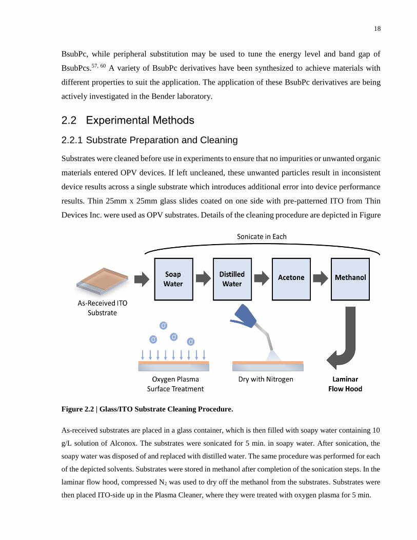


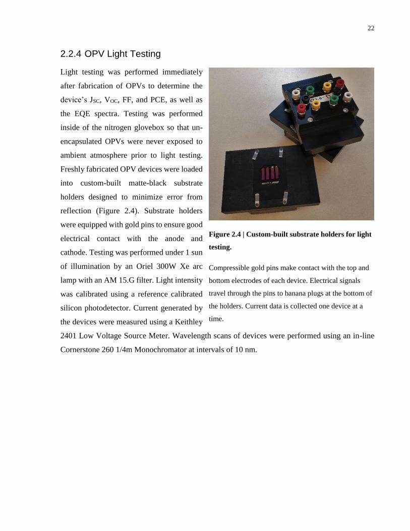


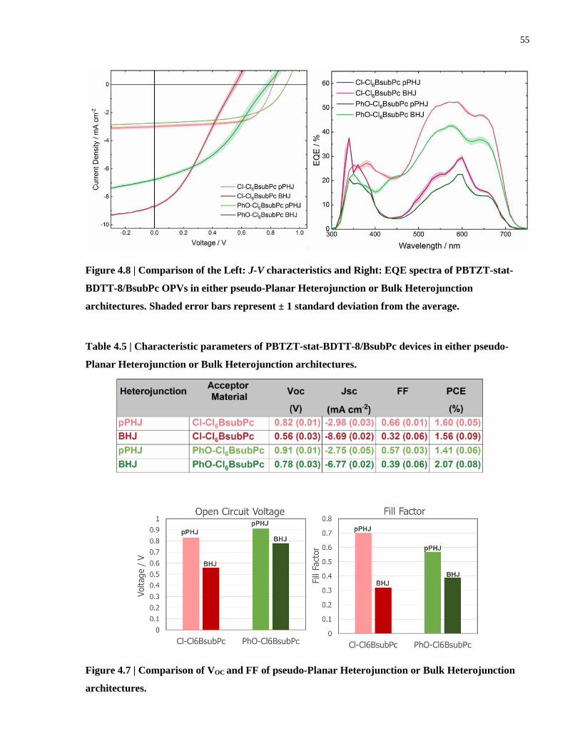


![Novel Boron Subphthalocyanines for Organic …...ITO indium doped tin oxide MoOx molybdenum oxide, indeterminate oxidation state MsO-BsubPc mezyl boron subphthalocyanine MTDATA 4,4',4"-tris[N,-(3-methylphenyl)-N-phenylamino]triphenylamine](https://static.documents.pub/doc/80x56/5fbeff8a40f4a94cd82710db/novel-boron-subphthalocyanines-for-organic-ito-indium-doped-tin-oxide-moox-molybdenum.jpg)


