Time T5A.1 Demonstration of 352-Gbit/s Single Line Rate PS-4096QAM THz Wired Transmission over Hollow-Core Fiber Junjie Ding 1 , Yanyi Wang 1 , Jiao Zhang 2 , Menghui He 1 , Feng Zhao 3 , Li Zhao 1 , Wen Zhou 1 , Yiwei Shi 1 , Min Zhu 2 , Jianjun Yu 1 1 Fudan University, China; 2 Purple Mountain Laboratories, China; 3 Xian University of Posts and Telecommunications, China We experimentally demonstrated THz wired transmission over 1-m hollow-core fiber employing 32-Gbaud PS-4096QAM signal at 325 GHz and successfully achieved the single line rate of 352 Gbit/s and the net spectrum efficiency of 8.6 bit/s/Hz. 19:30-19:45 T5A.2 Ultra-compact Single-shot Spectrometer Enabled by Stratified Waveguide Filters Ang Li 1 , Yeshaiahu Fainman 3 , Qixiang Cheng 2 , Shilong Pan 1 1 NUAA, China; 2 Cambridge University, United Kingdom; 3 UCSD, USA We demonstrate a silicon single-shot spectrometer with 0.008mm2 footprint, the smallest on CMOS compatible platforms. Experimental results confirm a bandwidth of 180nm with a resolution of 0.45nm. It opens new pathway towards commercial integrated spectrometers. 19:45-20:00 T5A.3 Aggregated 1.059 Tbit/s photonic-wireless transmission at 350 GHz over 10 meters Hongqi Zhang 1 , Lu Zhang 1 , Shiwei Wang 1 , Zijie Lu 1 , zuomin Yang 1 , Siqi Liu 1 , Xiaodan Pang 2 , Xianmin Zhang 1 , Xianbin Yu 1 1 Zhejiang University, China; 2 KTH, Sweden We report on a multi-dimensional multiplexed THz photonic wireless communication system. A record aggregated net rate of 1.059 Tbit/s over a wireless distance of 10 m in the 350 GHz band is experimentally demonstrated. 20:00-20:15 T5A.4 6.4Tb/s (16×400Gb/s) Nonlinear Frequency Division Multiplexing WDM Transmission over 640km SSMF We experimentally demonstrate nonlinear frequency division multiplexing WDM transmission over 640km SSMF with a record data capacity of 6.4Tb/s by employing the continuous nonlinear spectrum and neural network-based equalization in nonlinear frequency domain. 20:15-20:30 T5A.5 Real-time Single-Carrier 800Gb/s DP-64QAM Demonstration using Bi-Directional Self-homodyne Coherent Transceivers with 200krad/s Endless Active Polarization Controller Tao Gui 1 , Juntao Cao 1 , Xi Chen 1 , Keshuang Zheng 1 , Shuai Yuan 1 , Xiaotian Fang 1 , Yu Lei 2 , Qianxin Zhan 2 , Dawei Wang 2 , Qi Sui 2 , Zhaohui Li 2 , Liangchuan Li 1 1 Huawei Technologies, China; 2 School of Electronics and Information Technology, Sun Yat-Sen University, China We successfully demonstrated a real-time 800Gb/s single-carrier SHC-BiDi transmission with the proposed APC solution tracking up to a record 200 krad/s SOP rotation speed without performance penalty. A ~10km transmission without EDFA is achieved via a low cost DFB laser. 20:30-20:45 OSA 26th Optoelectronics and Communications Conference Post-deadline Session T5A (Room 7, 19:30-22:00, 6 July 2021) Presider: Alan P. T. Lau and Changyuan Yu, The Hong Kong Polytechnic University 1 Peking University, China 2 Peng Cheng Laboratory, Shenzhen, China Xinyu Chen 1 , Xiansong Fang 1 , Fan Yang 1 , Hao Ming 1 , Chenjia Li 1 , Lei Zhang 1 , Fan Zhang 1,2
Transcript
Time
T5A.1
Demonstration of 352-Gbit/s Single Line Rate PS-4096QAM THz Wired Transmission over Hollow-Core Fiber Junjie Ding1, Yanyi Wang1, Jiao Zhang2, Menghui He1, Feng Zhao3, Li Zhao1, Wen Zhou1, Yiwei Shi1, Min Zhu2, Jianjun Yu1 1Fudan University, China; 2Purple Mountain Laboratories, China; 3Xian University of Posts and Telecommunications, China We experimentally demonstrated THz wired transmission over 1-m hollow-core fiber employing 32-Gbaud PS-4096QAM signal at 325 GHz and successfully achieved the single line rate of 352 Gbit/s and the net spectrum efficiency of 8.6 bit/s/Hz.
19:30-19:45
T5A.2
Ultra-compact Single-shot Spectrometer Enabled by Stratified Waveguide Filters Ang Li1, Yeshaiahu Fainman3, Qixiang Cheng2, Shilong Pan1 1NUAA, China; 2Cambridge University, United Kingdom; 3UCSD, USA We demonstrate a silicon single-shot spectrometer with 0.008mm2 footprint, the smallest on CMOS compatible platforms. Experimental results confirm a bandwidth of 180nm with a resolution of 0.45nm. It opens new pathway towards commercial integrated spectrometers.
19:45-20:00
T5A.3
Aggregated 1.059 Tbit/s photonic-wireless transmission at 350 GHz over 10 meters Hongqi Zhang1, Lu Zhang1, Shiwei Wang1, Zijie Lu1, zuomin Yang1, Siqi Liu1, Xiaodan Pang2, Xianmin Zhang1, Xianbin Yu1 1Zhejiang University, China; 2KTH, Sweden We report on a multi-dimensional multiplexed THz photonic wireless communication system. A record aggregated net rate of 1.059 Tbit/s over a wireless distance of 10 m in the 350 GHz band is experimentally demonstrated.
20:00-20:15
T5A.4
6.4Tb/s (16×400Gb/s) Nonlinear Frequency Division Multiplexing WDM Transmission over 640km SSMF
We experimentally demonstrate nonlinear frequency division multiplexing WDM transmission over 640km SSMF with a record data capacity of 6.4Tb/s by employing the continuous nonlinear spectrum and neural network-based equalization in nonlinear frequency domain.
20:15-20:30
T5A.5
Real-time Single-Carrier 800Gb/s DP-64QAM Demonstration using Bi-Directional Self-homodyne Coherent Transceivers with 200krad/s Endless Active Polarization Controller Tao Gui1, Juntao Cao1, Xi Chen1, Keshuang Zheng1, Shuai Yuan1, Xiaotian Fang1, Yu Lei2, Qianxin Zhan2, Dawei Wang2, Qi Sui2, Zhaohui Li2, Liangchuan Li1 1Huawei Technologies, China; 2School of Electronics and Information Technology, Sun Yat-Sen University, China We successfully demonstrated a real-time 800Gb/s single-carrier SHC-BiDi transmission with the proposed APC solution tracking up to a record 200 krad/s SOP rotation speed without performance penalty. A ~10km transmission without EDFA is achieved via a low cost DFB laser.
20:30-20:45
OSA 26th Optoelectronics and Communications Conference Post-deadline Session T5A(Room 7, 19:30-22:00, 6 July 2021)
Presider: Alan P. T. Lau and Changyuan Yu, The Hong Kong Polytechnic University
1Peking University, China 2Peng Cheng Laboratory, Shenzhen, ChinaXinyu Chen1, Xiansong Fang1, Fan Yang1, Hao Ming1, Chenjia Li1, Lei Zhang1, Fan Zhang1,2
T5A.6
Single-Lane 402 Gb/s PAM-8 IM/DD Transmission Based on a Single DAC and an O-Band Commercial EML Md Sabbir-Bin Hossain1,2, Jinlong Wei1, Fabio Pittalà1, Nebojša Stojanović1, Stefano Calabrò1, Talha Rahman1, Tom Wettlin2, Changsong Xie1, Maxim Kuschnerov1, Stephan Pachnicke2 1Huawei Technologies Duesseldorf GmbH, Germany; 2Chair of Communications, Kiel University, Christian-Albrechts-Universitat zu Kiel, Kiel, Schleswig-Holstein, DE, academic, Germany We demonstrate 402 Gb/s IM/DD transmission using a single DAC directly driving an O-band EML with PAM-8. Considering 15.31%-overhead SD-FEC, this yields to a record net bit rate of 348.62 Gbit/s over 2 km SSMF.
20:45-21:00
T5A.7
High-speed Silicon Micro-Ring Modulator at 2-μm Waveband Weihong Shen1, Gangqiang Zhou1, Jiangbing Du1, Linjie Zhou1, Ke Xu2, Zuyuan He1 1Shanghai Jiao Tong University, China; 2Harbin Institute of Technology (Shenzhen), China Silicon micro-ring modulator with 18-GHz electro-optic bandwidth and <1-Vcm modulation efficiency was reported, achieving 50-Gbps highest-speed signaling at 1960 nm. Better endurance of two-photon absorption at 2 μm leads to significantly improved high-speed performances.
21:00-20:15
T5A.8
Field Trial of Cable Safety Protection and Road Traffic Monitoring over Operational 5G Transport Network with Fiber Sensing and On-Premise AI Technologies Ming-Fang Huang1, Shaobo Han1, Glenn Wellbrock2, Tiejun Xia2, Chaitanya Narisetty1, Milad Salemi1, Yuheng Chen1, James M. Moore3, Philip Ji1, Giovanni Milione1, Ting Wang1, Yukihide Yoda4, Yoshinori Kitahara4, Morio Ito4, Yoshiaki Aono4, Atsuo Itoh4 1NEC Laboratories America Inc, USA; 2Verizon, USA; 3Verizon, USA; 4NEC Corporation, Japan We report the distributed-fiber-sensing field trial results over a 5G-transport-network. A standard communication fiber is used with real-time AI processing for cable self-protection, cable-cut threat assessment and road traffic monitoring in a long-term continuous test.
20:15-21:30
T5A.9
Over 60GHz InP CDM and ICR Enabling 800Gbps LR/ER/ZR/ZR+ Transmission Links With 120Gbaud/DP-16QAM Modulation Jerome de You-Wei Chen1, Konstantin Kuzmin1, Maxime Poirier1, Tadatoshi Tomimoto1, George Zarris1, Ron Moore1, Chengkun Chen1, Wuchun Wu1, Jun Huang1, Marcel Boudreau1, Hui Xu1, Winston I. Way1 1NeoPhotonics, USA By using >60GHz 3dB bandwidth InP coherent driver modulator (CDM) and intradyne coherent receiver (ICR), we have demonstrated a record ≦13.6dB link budget for 800LR/ER, an rOSNR of 27dB for 600-km 800ZR+, and an 800ZR link accommodating optical line protection with a >20dB fiber loss budget.
21:30-21:45
T5A.10
Erbium-doped Waveguide Amplifier On Lithium Niobate On Insulator with 27.94 dB Total Gain and 6.20 dB/cm Net Gain Minglu Cai1, Kan Wu1, Junmin Xiang1, Jianping Chen1 1Shanghai Jiao Tong University, China. We demonstrate an erbium-doped waveguide amplifier on lithium niobate on insulator. The 2.58-cm long amplifier has 27.94 dB total gain (signal enhancement), 6.20 dB/cm net gain, and 3.48 dB noise figure at 1531.6 nm.
21:45-22:00
Demonstration of 352-Gbit/s Single Line Rate PS-4096QAM THz Wired Transmission over Hollow-Core Fiber
Junjie Ding1, Yanyi Wang1, Jiao Zhang2, Menghui He1, Feng Zhao3, Li Zhao1, Wen Zhou1, Yiwei Shi1, Min
Zhu2 and Jianjun Yu1* 1 Key Laboratory for Information Science of Electromagnetic Waves (MOE), Fudan University, Shanghai, China (*[email protected]);
2Purple Mountain Laboratories, Nanjing, Jiangsu, China; 3Xian University of Posts and Telecommunications, Xian, Shanxi, China
Since the ultra-wide bandwidth meets the urgent demand for large-capacity transmission, terahertz (THz)-wave communication has become a promising candidate technology in future 6G networks [1, 2]. Photonics-aided scheme has been demonstrated in THz transmission system to overcome the electromagnetic interference and bandwidth limitation of electronic equipment [2-4]. Furthermore, combined with the advanced high-order modulation, m-QAM THz signal generation and detection have been achieved to improve the transmission rate and spectral efficiency (SE) [3, 4]. By using probabilistically shaped 64-ary quadrature amplitude modulation (PS-64QAM), 2 × 300 Gbit/s line rate signal transmission at 320–380 GHz has been achieved in a THz photonic-wireless communication system [5]. However, the high loss resulted from large molecular absorption, high reflection loss, line-of-sight (LOS) and non-line-of-sight (NLOS) propagation characteristics is a critical problem for the future wireless links. To effectively solve this problem, it has been suggested that the system with newly developed THz hollow-core fiber (HCF) composed of a hollow substrate and a metal plating layer with a high reflectivity as the transmission medium could be one of the best ways for future 6G large capacity wireless communications [6, 7]. In our previous work, we have experimentally realized 128-Gbit/s W-band signal transmission over 1.5-m dielectric-coated metallic hollow fiber (DMHF) [8]. In this paper, we extend W-band wired delivery to THz band, and the deployed THz HCF can be applied in a wide wavelength range from visible light to far infrared and THz band. Besides, the THz loss characteristics of cladding modes propagating through the HCF is considered to be close to air loss window.
In this paper, the wired transmission of THz signal at 325 GHz over 1-m HCF in the photonics-aided THz-wave communication system is successfully demonstrated. By employing 32-Gbaud PS-4096QAM signal, the single line rate of the THz wired transmission reaches 352 Gbit/s (275.2-Gbit/s net rate) and the net SE is 8.6 bit/s/Hz, satisfying the 0.83-NGMI LDPC threshold with 25% overhead. The experimental results prove the potentiality of THz HCF as a new medium for high-speed transmission of THz signals.
2. Experimental setup
BinaryData
CCDM
LDPCEncoder
Amplitude Bits
Fold Index Bits SymbolMapping
U1 bits
U2 bits
sym2bin
PS-4096QAM11-bit/symbol
(b)
EA EA
PM-OCECL1
ECL2
I/Q MOD
EDFAOpticalATT UTC-PD
PC
1-m HCFEA
Mixer
LO
×24
200-GSa/s Digital OSC
(a)
Resampling
VNLEDD-LMSDecision
IQ Orthogonalization T/2 CMAFOE CPE
64-GSa/s AWG
Upsampling
Binary DataQAM Mapping
ResamplingRRC Filter
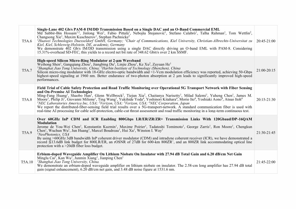
Fig. 1. (a) Experimental setup for transmission over THz HCF; (b) block diagram of PS-4096QAM signal generation.
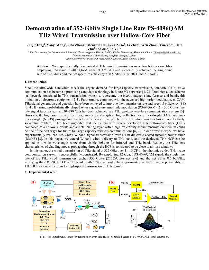
As shown in Fig. 1(a), we experimentally demonstrate the transmission of 32-Gbaud PS-QAM signals at 325 GHz over 1-m HCF in a photonics-aided THz communication system. For PS-QAM signal generation, we adopt the probabilistic amplitude shaping (PAS) scheme using a DVB-S2 LDPC encoder with 25% overhead (0.8 code rate), which is depicted in Fig. 1(b). The amplitude bits converted from the symbol sequence with different probabilities via constant composition distribution matcher (CCDM) are combined with fold index bits for PS symbol mapping. The probability distribution of the PS-4096QAM format with an information entropy of 11 bit/symbol is also given, which satisfies the Maxwell-Boltzmann distribution. In the Tx-side digital signal processing (DSP), the PS-QAM symbol sequence is ×2 up-sampled before root-raised-cosine (RRC) pulse shaping. The roll-off factor of RRC filter is set as 0.01 to overcome the system bandwidth limitation. The baseband electrical I/Q signals generated from a 64-GSa/s sampling rate arbitrary waveform generator (AWG) are boosted by two parallel electrical amplifiers (EAs) to drive the I/Q modulator. The optical carrier from the 100-kHz linewidth tunable ECL1 is modulated via an I/Q modulator with 30-GHz bandwidth, then amplified by a cascaded EDFA to compensate for the insertion loss of the modulator. The ECL2 is employed as the optical local oscillator (LO) and the frequency space between the two ECLs is 325 GHz. A polarization controller (PC) is added to adjust the polarization of the optical signal before the two laser beams are coupled by a polarization-maintaining optical coupler (PM-OC). The input optical power into the commercial uni-travelling photodiode (UTC-PD) is adjusted through a variable optical attenuator (VOA). Subsequently, the generated THz signal at 325 GHz from the UTC-PD is fed into 1-m THz HCF. The cross section of the HCF is illustrated in Fig. 2(a). Here, polycarbonate (PC) tube is used as the hollow substrate of the THz HCF to obtain flexibility, which can be bent or even coiled. The inner metal plating layer is silver film, the thickness of which is 0.3 µm. In addition, the inner diameter of the THz HCF is 3.6 mm and the linear transmission loss at 300 GHz is 1.33 dB/m [9, 10].
At the receiver, the THz signal after HCF transmission is received by a horn antenna. As shown in the photo of the experimental setup in Fig. 2(b), the two antennas at the transmitter and the receiver are placed in a parallel and equidirectional way. The HCF is bent and precisely inserted between the two antennas to ensure that the THz signal is confined in the HCF without leakage. The received THz signal is down-converted to the intermediate-frequency (IF) signal at 17 GHz by a 24-order harmonic THz Schottky mixer driven by an electrical LO. The amplified IF signal after an EA is then sampled by a real-time oscilloscope with 59-GHz electrical bandwidth and 200-GSa/s sampling rate. For 32-Gbaud PS-4096QAM THz signal transmission, the optical spectrum of the signal into PD with a frequency space of 325 GHz and a resolution of 0.01 nm is illustrated in Fig. 2(c). The center frequency of the THz signal is thus 325 GHz. Meanwhile, the electrical spectrum of the received IF signal at 17 GHz is given in Fig. 2(d).
The offline Rx-side DSP includes resampling, I/Q orthogonalization as well as 21-tap T/2-spaced CMA
equalization. After frequency offset estimation (FOE), we use hybrid principal component-based phase estimation
Receiver
Transmitter UTC-PD
1-m HCF
Mixer
LO
(a)325 GHz
IF 17 GHz
(c)
(d)
(b)
Air coreMetal layerSubstrate
Fig. 2. (a) The cross section of the HCF; (b) photo of the experimental setup; (c) optical spectrum of 32-Gbaud PS-4096QAM optical signal
into PD; (d) electrical spectrum of the received IF signal.
and blind phase search (PCPE-BPS) algorithms in carrier phase estimation (CPE) step. 190-tap 2nd Volterra nonlinear equalization (VNLE) is deployed to reduce the nonlinear distortions resulting from the optoelectronic devices. Moreover, a 61-tap DD-LMS equalizer is finally utilized to compensate for residual linear impairment.
3. Results and discussion
Figs. 3(a) and (b) shows the calculated NGMI of 32-Gbaud PS-256QAM, PS-1024QAM and PS-4096QAM signals versus power into PD in back-to-back (BtB) case and after 1-m HCF transmission, respectively. The information entropy of PS-256QAM, PS-1024QAM and PS-4096QAM is set as 7.8 bit/symbol, 9.6 bit/symbol and 11 bit/symbol, respectively. Considering the LDPC code with 0.8 code rate, the line bit rate of 32-Gbaud PS-4096QAM signal is 11 × 32= 352 Gbit/s, while the net bit rate is [11-12 × (1-0.8)] × 32= 275.2 Gbit/s. The net SE is thus 8.6 bit/s/Hz. NGMI is an outstanding channel metric which can evaluate the SD-FEC code performance regardless of the QAM order [11]. If the pre-FEC QAM data reaches an NGMI of 0.8, error-free post-FEC results will be obtained by an ideal SD-FEC code with 0.8 code rate. However, the used DVB-S2 LDPC has a gap to the theoretic limit and the error-free decoding is achieved for different modulation formats when NGMI is 0.83 [12]. Therefore, 0.83 NGMI is used as the LDPC threshold in this paper.
In BtB case, the measured NGMI values of PS-256QAM and PS-1024QAM signals are all above the 0.83-NGMI LDPC threshold. For PS-4096QAM signal, post-FEC error free can be obtained when the input power into PD reaches 10 dBm. Besides, compared with the BtB case, there is around 0.5-dB power penalty after 1-m HCF transmission. The required power into PD is improved to 10.5 dBm for PS-4096QAM signal in HCF transmission case, considering the 0.83-NGMI LDPC threshold. Meanwhile, the required power into PD for PS-1024QAM signal at 0.83-NGMI threshold is 8.6 dBm. Moreover, when the power into PD is 12 dBm, the constellation diagrams of the recovered PS-1024QAM and PS-4096QAM symbols are also illustrated in Fig. 3, respectively.
4. Conclusions
We have experimentally demonstrated 32-Gbaud PS-4096QAM THz signal wired transmission at 325 GHz over 1-m HCF in the photonics-aided THz-wave communication system. With the aid of PS technology and advanced DSP, 352-Gbit/s line rate (275.2-Gbit/s net rate) transmission with net SE of 8.6 bit/s/Hz can be successfully realized, satisfying the 0.83-NGMI LDPC threshold. This work is supported by National Key R&D Programmes of China (2018YFB1800905) and National Natural Science Foundation of China (61935005, 91938202, 61922025, 61527801, 61675048, 61720106015, 61835002, 61875164, and 61805043).
5. References [1] K. Takiguchi et al., “Flexible data rate THz-wave communication using Nyquist pulses and optical-domain reception…,” OFC 2020, M4I.5. [2] S. R. Moon et al., “Cost-Effective Photonics-Based THz Wireless Transmission…,” J. Light. Technol., vol. 39, no. 2, pp. 357-362, 2021. [3] X. Li et al., “Photonics-aided 2×2 MIMO wireless terahertz wave signal…,” Opt. Express, vol. 25, no. 26, pp. 33236–33242, 2017. [4] K. Wang et al., “Probabilistically shaped 16QAM signal transmission in a photonics-aided wireless terahertz-wave…,” OFC 2018, M4J.7. [5] S. Jia et al., “2 × 300 Gbit/s line rate PS-64QAM-OFDM THz photonic-wireless…,” J. Light. Technol., vol. 38, no.17, pp. 4715-4721, 2020. [6] V. Sharif et al., “Terahertz Hollow-Core Optical Fibers for Efficient Transmission of Orbital Angular…,” J. Light. Technol., 2021. [7] Y. Hou et al., “Terahertz single polarization single-mode hollow-core fiber…,” Photon. Technol. Lett., vol. 24, no. 8, pp. 637-639, 2012. [8] J. Yu et al., “High-Speed Signal Transmission at W-Band Over…,” IEEE Trans. Microw. Theory Tech., vol. 63, no. 6, pp. 1836-1842, 2015. [9] K. Chen et al., “Characterization of gas absorption modules based on flexible mid-infrared hollow…,” Sensors, vol. 19, no. 7, pp. 1698, 2019. [10] M. He et al., “Transmission and imaging characteristics of flexible…,” Opt. Express, vol. 29, no. 6, pp. 8430-8440, 2021. [11] J. Cho et al., “Normalized generalized mutual information as a forward error correction threshold…,” ECOC 2017, M2D.2. [12] K. Wang et al., “Bi-Directional OFDM Truncated PS-4096QAM Signals …,” J. Light. Technol., vol. 39, no. 11, pp. 3412-3419, 2021.
(a) (b)
Fig. 3. (a) NGMI of three PS-QAM formats versus power into PD (a) in BtB case and (b) after 1-m HCF transmission.
Ultra-compact Single-shot Spectrometer Enabled by Stratified Waveguide Filters
Ang Li1,*, Yeshaiahu Fainman2, Qixiang Cheng3, Shilong Pan1 1. Key Laboratory of Radar Imaging and Microwave Photonics, Ministry of Education, Nanjing University of Aeronautics and Astronautics,
Nanjing 210016, China 2. Department of Electrical and Computer Engineering, University of California at San Diego, La Jolla, CA, USA
3. Department of Engineering, University of Cambridge, 9 JJ Thomson Avenue, Cambridge CB3 0FA, UK Author e-mail address: [email protected]
Single-shot spectrometers being able to reconstruct unknown optical spectrum with single measurement are extremely useful in astronomy, environmental science, biomedical applications etc. There exists a rapidly expanding application space that has stronger desire for portability, lightweight and low-cost spectrometers, such as unmanned aerial vehicle (UVA) based remote sensing, alien exploration, in-home health monitoring etc. Among all material platforms, silicon photonics is most promising due to its ultra-high index contrast that allows high integration density of photonic components in a small chip as well as its compatibility with mature CMOS manufacturing technology that facilities massive fabrication of photonic integrated circuit at low-cost. Conventional single-shot spectrometer realized on silicon photonics platform split the spectral contents of the incident signal to multiple channels and record individual intensity. The spectral splitter can be dispersive gratings or narrowband filters array as shown in Fig. 1[1, 2]. This approach is requires a large number of splitting channels and detectors, when targeting broad bandwidth BW and high resolution ∆𝜆, as the channel number N=BW/∆𝜆. This will in turn cause considerably large footprint, hardware cost, and degraded signal-to-noise ratio (SNR) at each detector. How to produce comparative performance, namely operation bandwidth and spectral resolution, while maintaining compact footprint and high SNR remains a challenge.
Fig. 1 Conventional single-shot spectrometers utilize either narrowband filters or dispersive gratings
to spatially split the spectral contents of the incident signal.
In this paper, we address this by developing a computational single-shot spectrometer which consists of 32 stratified waveguide filters with diverse transmission spectra covering a broad wavelength span[3]. Each filter’s transmission spectrum can be considered as a set of sampling coefficients at each wavelength points. Together with advanced signal processing algorithms, the incident spectrum can be reconstructed from the outputs of 32 filters. Moreover, we also develop a tap-based ultra-compact 1x32 power splitter for directing incident signal into 32 filters. The 32 filters and the 1x32 splitter, demonstrated on silicon photonics platform, in total occupies a footprint less than 0.008mm2, which is the smallest spectrometer realized on a CMOS compatible platform. The experimental results confirm a broad operation bandwidth of 180nm as well as a high spectral resolution of 0.45nm.
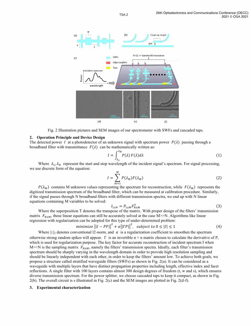
Fig. 2 Illustration pictures and SEM images of our spectrometer with SWFs and cascaded taps.
2. Operation Principle and Device Design The detected power 𝐼 at a photodetector of an unknown signal with spectrum power 𝑃(𝜆) passing through a broadband filter with transmittance 𝐹(𝜆) can be mathematically written as:
𝐼 = ∫ 𝑃(𝜆)𝜆𝑁
𝜆1
𝐹(𝜆)𝑑𝜆 (1)
Where 𝜆1, 𝜆𝑁 represent the start and stop wavelength of the incident signal’s spectrum. For signal processing, we use discrete form of the equation:
𝐼 = ∑ 𝑃(𝜆𝑀)𝐹(𝜆𝑀)𝑀
𝑚=1
(2)
𝑃(𝜆𝑀) contains M unknown values representing the spectrum for reconstruction, while 𝐹(𝜆𝑀) represents the digitized transmission spectrum of the broadband filter, which can be measured at calibration procedure. Similarly, if the signal passes through N broadband filters with different transmission spectra, we end up with N linear equations containing M variables to be solved:
𝐼1𝑥𝑁 = 𝑃1𝑥𝑀𝐹𝑁𝑥𝑀𝑇 (3)
Where the superposition T denotes the transpose of the matrix. With proper design of the filters’ transmission matrix 𝐹𝑁𝑥𝑀, these linear equations can still be accurately solved at the case M>>N. Algorithms like linear regression with regularization can be adopted for this type of under-determined problem:
Where ||·||2 denotes conventional l2-norm, and 𝛼 is a regularization coefficient to smoothen the spectrum otherwise strong random spikes will appear. Γ is an invertible n × n matrix chosen to calculate the derivative of P, which is used for regularization purpose. The key factor for accurate reconstruction of incident spectrum I when M<<N is the sampling matrix 𝐹𝑁𝑥𝑀, namely the filters’ transmission spectra. Ideally, each filter’s transmission spectrum should be sharply varying in the wavelength domain in order to provide high resolution sampling and should be linearly independent with each other, in order to keep the filters’ amount low. To achieve both goals, we propose a structure called stratified waveguide filters (SWFs) as shown in Fig. 2(a). It can be considered as a waveguide with multiple layers that have distinct propagation properties including length, effective index and facet reflections. A single filter with 100 layers contains almost 300 design degrees of freedom (t, w and s), which ensures diverse transmission spectrum. For the power splitter, we choose cascaded taps to keep it compact, as shown in Fig. 2(b). The overall circuit is s illustrated in Fig. 2(c) and the SEM images are plotted in Fig. 2(d-f).
The device containing 32 SWFs was fabricated on a 200mm silicon-on-insulator wafer using Ebeam lithography. However, all the design parameters are chosen to be compatible with standard CMOS technology that uses optical lithography. First of all, we measure the filters’ transmission spectra and record them as sampling matrix. Some representative results are plotted in Fig. 3(a). Clearly, the filters’ transmission spectra satisfy the both criteria introduced in previous section. Afterwards, various spectra including broadband spectrum from a SLD and narrow linewidth laser from Agilent 8163B tunable laser were sent to the spectrometer to calibrate the regularization coefficients. After calibration, we send another broadband spectrum from a C+L ASE source and narrow linewidth laser peaks at various wavelength locations for reconstruction using the regularization coefficients obtained in calibration procedure. During the entire measurement procedure, the chip and the background temperature is stabilized using a vacuum pump and a temperature controller, respectively. As can be seen in Fig. 3(b-d), both broadband spectral components and narrow linewidth peaks can be accurately reconstructed using these 32 stratified waveguide filters. The operation bandwidth is tested to be 180nm, which is limited by our measurement equipment, to be specific, the tunable laser we used to measure the filters’ transmission spectra. And the resolution, defined as the Full-Width-Half-Maxim of the laser peak that can be clearly resolved, is about 0.45nm.
Fig. 3 Experimental characterization of our spectrometer
4. Conclusion
In this manuscript, we implement a concept of a single-shot spectrometer that uses an array of broadband SWFs realized in silicon photonics platforms. The rich design degrees of freedom of each SWF enable the spectral filters with sharply varying spectral features as well as low linear dependency between any two filters. As a consequence, the spectrometer consisting of only 32 filters can reconstruct both broadband spectral components and narrow linewidth peaks accurately. In order to distribute the incident spectral signal into 32 filters with little power imbalance, we also developed and demonstrated experimentally an ultra-compact splitter based on cascaded taps. The total footprint of the splitter and the 32 SWFs is as small as 35 μm × 260 μm, which to the best of our knowledge, is the smallest experimentally demonstrated spectrometer on a silicon photonic platform. The experimental results demonstrate operation with broad bandwidth input signals (i.e., 180 nm centered at 1550 nm) and narrowband signals (i.e., 0.45 nm FWHM laser emission). The SWF spectrometer approach is a promising candidate for cost-effective manufacturing of miniaturized spectrometers.
1. Gatkine, P., et al., Arrayed waveguide grating spectrometers for astronomical applications: new results.
Optics Express, 2017. 25(15): p. 17918-17935. 2. Fan, T., et al., Highly-uniform resonator-based visible spectrometer on a Si 3 N 4 platform with robust and
accurate post-fabrication trimming. Optics Letters, 2018. 43(20): p. 4887-4890. 3. Li, A. and Y. Fainman, On-chip spectrometers using stratified waveguide filters. Nature Communications,
1. Introduction With the rapid growth of Internet users and wireless data traffic, the demand for wireless service is projected to grow dramatically. The capacity demand for wireless connections is predicted to exceed 100 Gbit/s and even up to Tbit/s in the coming decades. The terahertz (THz) band (0.3–10 THz), featuring high energy efficiency and large bandwidth, is envisioned as a promising candidate to accommodate the ever-increasing capacity demand [1,2]. Benefit from the rapid evolution of state-of-the-art THz devices as well as the wide deployment and large bandwidth of optical fibers, significant progress has been witnessed in the photonic-assisted THz communication system [3-12]. For instance, single-channel wireless transmission of 100 Gbit/s at 280 GHz, 106 Gbit/s at 400 GHz, and 128 Gbit/s at 300 GHz over 0.5 m are experimentally demonstrated [3-5] without any multiplexing techniques. To further improve the data rates, the multiplexing techniques such as polarization multiplexing (PDM), wavelength division multiplexing (WDM) are employed in sub-THz/THz wireless systems. For example, wireless transmission with 108 Gbit/s at 100 GHz based on the PDM method [11], wireless transmission of 260 Gbit/s at 400 GHz based on the WDM method [12] are experimentally obtained. Based on these single-dimensional multiplexing schemes, wireless data rates have indeed significantly improved. However, it is insufficient to support wireless data rates up to Tbit/s and beyond due to the limitation of obtainable signal-to-noise ratio (SNR) after hybrid photonic wireless transmission. Therefore, a multi-dimensional multiplexing scheme targeting Tbit/s is highly desirable in this sense.
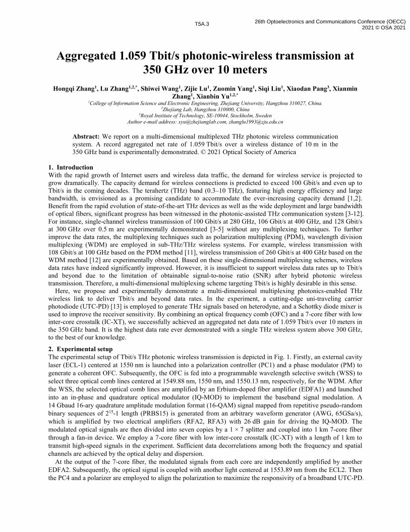
Here, we propose and experimentally demonstrate a multi-dimensional multiplexing photonics-enabled THz wireless link to deliver Tbit/s and beyond data rates. In the experiment, a cutting-edge uni-traveling carrier photodiode (UTC-PD) [13] is employed to generate THz signals based on heterodyne, and a Schottky diode mixer is used to improve the receiver sensitivity. By combining an optical frequency comb (OFC) and a 7-core fiber with low inter-core crosstalk (IC-XT), we successfully achieved an aggregated net data rate of 1.059 Tbit/s over 10 meters in the 350 GHz band. It is the highest data rate ever demonstrated with a single THz wireless system above 300 GHz, to the best of our knowledge.
2. Experimental setup The experimental setup of Tbit/s THz photonic wireless transmission is depicted in Fig. 1. Firstly, an external cavity laser (ECL-1) centered at 1550 nm is launched into a polarization controller (PC1) and a phase modulator (PM) to generate a coherent OFC. Subsequently, the OFC is fed into a programmable wavelength selective switch (WSS) to select three optical comb lines centered at 1549.88 nm, 1550 nm, and 1550.13 nm, respectively, for the WDM. After the WSS, the selected optical comb lines are amplified by an Erbium-doped fiber amplifier (EDFA1) and launched into an in-phase and quadrature optical modulator (IQ-MOD) to implement the baseband signal modulation. A 14 Gbaud 16-ary quadrature amplitude modulation format (16-QAM) signal mapped from repetitive pseudo-random binary sequences of 215-1 length (PRBS15) is generated from an arbitrary waveform generator (AWG, 65GSa/s), which is amplified by two electrical amplifiers (RFA2, RFA3) with 26 dB gain for driving the IQ-MOD. The modulated optical signals are then divided into seven copies by a 1 × 7 splitter and coupled into 1 km 7-core fiber through a fan-in device. We employ a 7-core fiber with low inter-core crosstalk (IC-XT) with a length of 1 km to transmit high-speed signals in the experiment. Sufficient data decorrelations among both the frequency and spatial channels are achieved by the optical delay and dispersion.
At the output of the 7-core fiber, the modulated signals from each core are independently amplified by another EDFA2. Subsequently, the optical signal is coupled with another light centered at 1553.89 nm from the ECL2. Then the PC4 and a polarizer are employed to align the polarization to maximize the responsivity of a broadband UTC-PD.
The modulated optical carrier centered at 1550 nm and the unmodulated local oscillator (LO) lightwave at 1553.89 nm are separated by 350 GHz. The modulated light consists of three wavelengths with equal spacing of 15 GHz. Combined with the unmodulated LO lightwave, a 3-channel THz signal is generated in the UTC-PD. The generated THz channels are centered at 365 GHz, 350 GHz, and 335 GHz and are named channel_1 (Ch_1), channel_2 (Ch_2), and channel_3 (Ch_3), respectively. Subsequently, the THz signals from the UTC-PD are radiated into a 10 m line-of-sight (LOS) wireless link via a horn antenna. A pair of THz lenses with 25 dBi gain are used to collimate the THz beam to reduce the propagation path loss.
At the receiver side, a Schottky mixer is used to down-convert the received THz signals into the intermediate frequency (IF) domain, which is driven by a 12-order frequency multiplied electrical signal. The LO signal is located at 372.5 GHz. Finally, the IF signals are amplified by an electrical amplifier (RFA4) with 22 dB gain and then sampled by a real-time digital storage oscilloscope (DSO, 160GSa/s) for offline DSP.
Fig. 1. Experimental setup of Tbit/s THz photonics wireless communication link. ECL: external cavity laser; PC: polarization controller; PM: phase modulator; RF: radio frequency; RFA: RF amplifier; WSS: wavelength selective switch; EDFA: erbium-doped fiber amplifier; AWG: arbitrary waveform generator; IQ-MOD: in-phase and quadrature modulator; VOA: variable optical attenuator; UTC-PD: uni-traveling carrier photodiode; DSO: digital storage oscilloscope; LO: local oscillator. The insert: (a) optical spectra of optical frequency comb after the PM. (b) optical spectra at the input of the UTC-PD.
3. Experimental results and discussions Fig. 2 shows the experimental results. Fig. 2(a) presents the measured bit-error-rate (BER) performance as a function of the optical power at the UTC-PD for in total 21 channels after the 7-core fiber and 10-m wireless transmission. As the optical power increases, the BER performances of all channels becomes better. For the same frequency channel within different cores, the BER performances constantly form a cluster with negligible penalties. The BER performances of all 21 channels can reach below the soft decision forward-error-correction (SD-FEC, 2.7 × 10⁻²) threshold with 20% overhead [14]. Besides, the BER performances of Ch_1 and Ch_2 in all cores can reach below the hard decision forward-error-correction (HD-FEC, 4.5 × 10⁻³) threshold with 7% overhead [15]. Subsequently, each core of 7-core fiber carries data rates of 168 Gbit/s (14 Gbaud × 4 bit/s/Hz × 3 channels), resulting in an aggregate line data rate of 1.176 Tbit/s (168 Gbit/s × 7) in the 7-core fiber. Taking the FEC overhead into account, an aggregated net data rate of 1.059 Tbit/s after hybrid photonics wireless transmission is successfully achieved. Owing to the limitation of the Schottky mixer (~40 GHz bandwidth), the Ch_3 is with the worst performance.
Fig. 2(b) depicts the measured baud rate-dependent BER performance of the core_5 for three channels as an example. As the baud rate increases, the BER performance worsens with narrower guardband between adjacent channels and more crosstalk. Besides, another main reason for BER degradation is the reduction of electrical SNR. The BER performance of all 3-channel can reach below the HD-FEC when the baud rate is lower than 10 Gbaud. We also test the system stability for selective 3 channels - core_1, core_3, and core_5, as shown in Fig. 2(c). In terms of BER performance, three channels individually possess stable performance with negligible variation over 300 measured traces, while features different performance channel by channel, as observed in Fig. 2(a). In addition, Fig. 2(d) shows the measured BER performance of 3 channels over core_1 with different wireless transmission distances, as an example. As the wireless transmission distance increases from 6 m to 8 m, we can see the BER
performance slightly degrades in general. Furthermore, when the distance further increases to 10 m, the BER performance variation can also be observed, mainly caused by the alignment accuracy variation of the THz transmitter and receiver.
Fig. 2. Experimental results of Tbit/s wireless transmission. (a) The measured BER performance of 7-core fiber with overall 21 channels after 7-core fiber and 10 m wireless transmission. (b) The measured 3-channel BER performance of core_5 versus baud rate. (c) System stability of 3-channel in core_1, core_3, and core_5. (d) The measured BER performance of 3-channel in core_1 with different wireless distances.
4. Conclusions We have experimentally demonstrated a record aggregated net rate of 1.059 Tbit/s with a single multi-dimensional multiplexed photonic-wireless transmission system, enabled by both frequency and spatial division multiplexing. Transmission over 10 m wireless distance is achieved in the 350 GHz band. Our work can be considered a significant milestone to pave the way towards Tbit/s wireless communications.
Acknowledgments This work is supported by the National Key Research and Development Program of China (2020YFB1805700), in part by the Natural National Science Foundation of China under Grant 61771424, the Natural Science Foundation of Zhejiang Province under Grant LZ18F010001 and LQ21F010015, the Swedish Research Council 2019-05197_VR, State Key Laboratory of Advanced Optical Communication Systems and Networks of Shanghai Jiao Tong University, the Fundamental Research Funds for the Central Universities 2020QNA5012 and Zhejiang Lab (no. 2020LC0AD01).
References [1] V. Petrov, et al., in ICUMT, 2016, 183-190. [2] I. F. Akyildiz, et al., Phys. Commun-Amst. 12, 16-32 (2014). [3] V. K. Chinni, et al., Electron. Lett. 54, 638-640, (2018). [4] S. Jia, et al., J. Light. Technol. 36, 610-616, (2018). [5] C. Castro, et al., in OFC, 2019, paper M4F. 5. [6] T. Nagatsuma, et al., in MWP, 2016, 27-30. [7] X. Yu, et al., APL Photon. 1, 081301 (2016). [8] H. Hamada, et al., in IMS, 2018, 1480-1483.
[9] H. Shams, et al., IEEE Photon. J. 7, 1-11 (2015). [10] K. Liu, et al., IEEE Photon. Technol. Lett. 30, 1064-1067 (2018). [11] X. Li, et al., Opt. Express. 21, 18812-18819, (2013). [12] X. Pang, et al., in Proc. IPC 2016, Paper PD1-2. [13] H. Ito, et al., Electron. Lett. 36, 1809-1810 (2000). [14] D. Chang, et al., in Proc. OFC/NFOEC, 2012, 1-3. [15] S. Koenig, et al., Nat. Photonics, 7, 977-981 (2013).
6.4Tb/s (16×400Gb/s) Nonlinear Frequency Division Multiplexing WDM Transmission over 640km SSMF
Xinyu Chen1, Xiansong Fang1, Fan Yang1, Hao Ming1, Chenjia Li1, Lei Zhang1, Fan Zhang1, 2, *
1State Key Laboratory of Advanced Optical Communication Systems and Networks, Frontiers Science Center for Nano-optoelectronics, Department of Electronics, Peking University, Beijing 100871, China
Nonlinear frequency division multiplexing (NFDM) has attracted great attention recently as a revolutionary transmission scheme to treat fiber nonlinearity as a constructive effect, rather than a destructive feature [1]. This approach uses nonlinear Fourier transform (NFT) against Kerr nonlinear distortions with data modulated on the nonlinear spectrum that evolves linearly in the fiber channel, which contains discrete spectrum and continuous spectrum [2]. Over the past few years, significant progress has been made in both numerical [3-5] and experimental [6-7] studies of NFDM transmission, which aims to design tailored transmission and detection strategies for enhancing the achievable capacity of the NFDM systems. Up to now, however, due to many challenges in design and practical implementation, there is still a certain gap between the demonstrated experimental NFDM systems and the high-capacity transmission. The highest data rate so far achieved a net data rate of single-wavelength 220Gb/s in dual-polarization (DP) NFDM system with continuous spectrum modulation over 976km standard single-mode fiber (SSMF) [6]. To further extend the data capacity and prompt the performance of NFDM systems, it is necessary to increase the single lane data rate and combine NFDM with wavelength division multiplexing (WDM). In this paper, we demonstrate a 64Gbaud 16-ary quadrature amplitude modulation (16QAM) continuous spectrum modulated DP-NFDM WDM system over 640km SSMF with a record data rate of 6.4Tb/s (16×400Gb/s) by employing neural network (NN) based equalization [4].
2. DP-NFDM System Model
The block diagram of the q-modulated NFDM system is depicted in Fig. 1. The useful temporal consecutive signal is required to be separated so that the vanishing boundary conditions of the NFT operation are satisfied. Owing to the temporal broadening caused by chromatic dispersion, certain guard intervals (GI) are essential to avoid inter-symbol interference (interval time GT ). Here we define the guard interval factor g as the total burst time duration
0 GT T+ over the useful time duration 0T . For the sake of shortening GI, pre-dispersion compensation (PDC) is applied [7]. The time domain signal is generated via the inverse nonlinear Fourier transform (INFT). After coherent detection at the receiver, NFT is performed to recover ( )cQ , followed by a phase back-rotation operation which removes the interplay of dispersion and nonlinearity during propagation. Finally, the data decoding is performed.
Fig. 1. Principle of the NFDM system.
3. Experimental Setup and Results
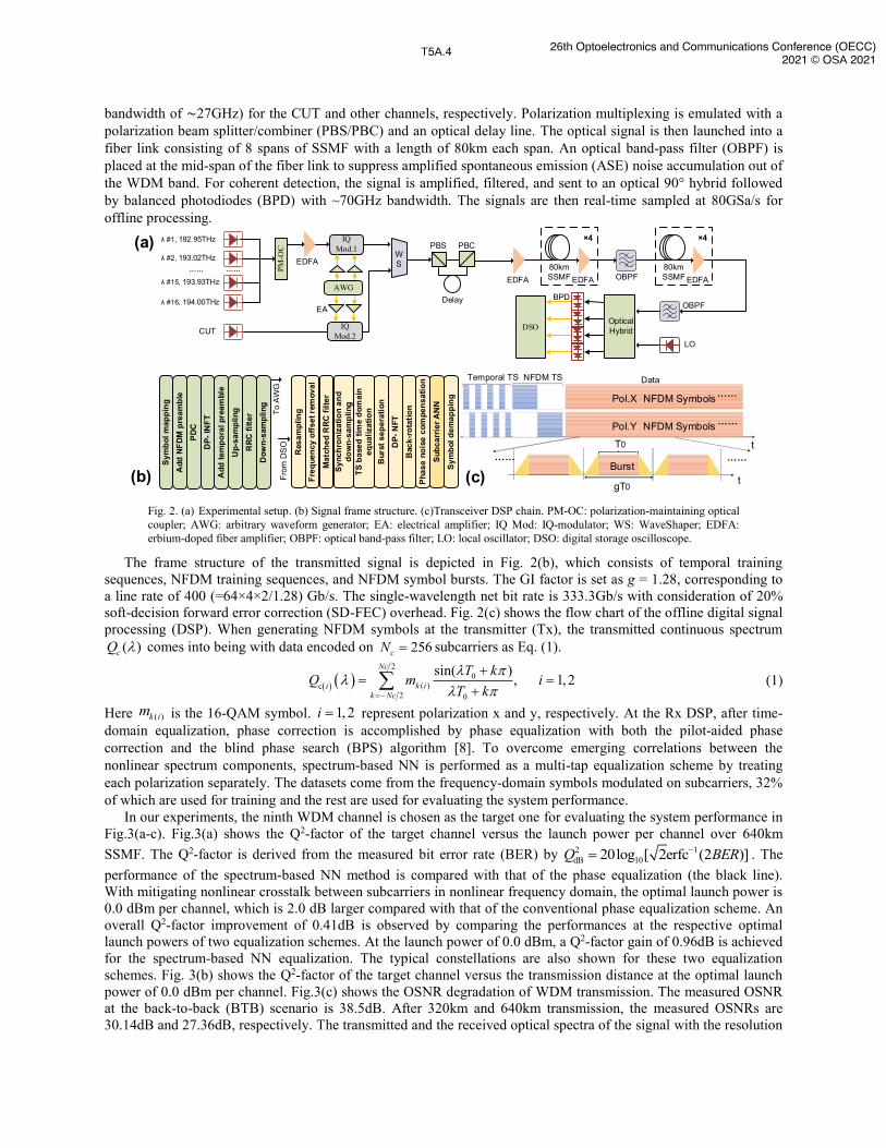
We set up a WDM system with 16×64Gbaud DP-NFDM 16QAM signals with 70GHz channel spacing. The experimental setup is shown in Fig.2(a). The loading channels were from 16 external cavity lasers (ECLs) at frequencies from 192.95 THz to 194.00 THz, which were then switched off in turn before multiplexing with the channel under test (CUT) using a WaveShaper (WS). The baseband signal was generated with an arbitrary waveform generator (AWG) operating at 120GSa/s. After amplified by a pair of electrical amplifiers (EAs) with 50GHz bandwidth, the waveforms from AWG were used to drive the IQ modulators (IQ Mod.1/2 with a 3dB
bandwidth of ∼27GHz) for the CUT and other channels, respectively. Polarization multiplexing is emulated with a polarization beam splitter/combiner (PBS/PBC) and an optical delay line. The optical signal is then launched into a fiber link consisting of 8 spans of SSMF with a length of 80km each span. An optical band-pass filter (OBPF) is placed at the mid-span of the fiber link to suppress amplified spontaneous emission (ASE) noise accumulation out of the WDM band. For coherent detection, the signal is amplified, filtered, and sent to an optical 90° hybrid followed by balanced photodiodes (BPD) with ~70GHz bandwidth. The signals are then real-time sampled at 80GSa/s for offline processing.
The frame structure of the transmitted signal is depicted in Fig. 2(b), which consists of temporal training sequences, NFDM training sequences, and NFDM symbol bursts. The GI factor is set as g = 1.28, corresponding to a line rate of 400 (=64×4×2/1.28) Gb/s. The single-wavelength net bit rate is 333.3Gb/s with consideration of 20% soft-decision forward error correction (SD-FEC) overhead. Fig. 2(c) shows the flow chart of the offline digital signal processing (DSP). When generating NFDM symbols at the transmitter (Tx), the transmitted continuous spectrum
( )cQ comes into being with data encoded on 256cN = subcarriers as Eq. (1).
( ) ( )2
0( )c
2 0
sin( ), 1, 2
Nc
k iik Nc
T kQ m i
T k
=−
+= =
+ (1)
Here ( )k im is the 16-QAM symbol. 1, 2i = represent polarization x and y, respectively. At the Rx DSP, after time-domain equalization, phase correction is accomplished by phase equalization with both the pilot-aided phase correction and the blind phase search (BPS) algorithm [8]. To overcome emerging correlations between the nonlinear spectrum components, spectrum-based NN is performed as a multi-tap equalization scheme by treating each polarization separately. The datasets come from the frequency-domain symbols modulated on subcarriers, 32% of which are used for training and the rest are used for evaluating the system performance.
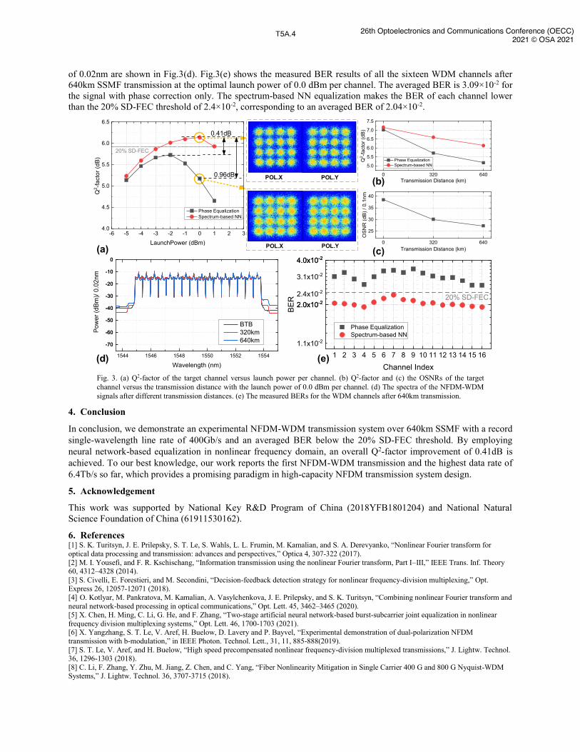
In our experiments, the ninth WDM channel is chosen as the target one for evaluating the system performance in Fig.3(a-c). Fig.3(a) shows the Q2-factor of the target channel versus the launch power per channel over 640km SSMF. The Q2-factor is derived from the measured bit error rate (BER) by 2 1
dB 1020log [ 2erfc (2 )]Q BER−= . The performance of the spectrum-based NN method is compared with that of the phase equalization (the black line). With mitigating nonlinear crosstalk between subcarriers in nonlinear frequency domain, the optimal launch power is 0.0 dBm per channel, which is 2.0 dB larger compared with that of the conventional phase equalization scheme. An overall Q2-factor improvement of 0.41dB is observed by comparing the performances at the respective optimal launch powers of two equalization schemes. At the launch power of 0.0 dBm, a Q2-factor gain of 0.96dB is achieved for the spectrum-based NN equalization. The typical constellations are also shown for these two equalization schemes. Fig. 3(b) shows the Q2-factor of the target channel versus the transmission distance at the optimal launch power of 0.0 dBm per channel. Fig.3(c) shows the OSNR degradation of WDM transmission. The measured OSNR at the back-to-back (BTB) scenario is 38.5dB. After 320km and 640km transmission, the measured OSNRs are 30.14dB and 27.36dB, respectively. The transmitted and the received optical spectra of the signal with the resolution
of 0.02nm are shown in Fig.3(d). Fig.3(e) shows the measured BER results of all the sixteen WDM channels after 640km SSMF transmission at the optimal launch power of 0.0 dBm per channel. The averaged BER is 3.09×10⁻² for the signal with phase correction only. The spectrum-based NN equalization makes the BER of each channel lower than the 20% SD-FEC threshold of 2.4×10⁻², corresponding to an averaged BER of 2.04×10⁻².
Fig. 3. (a) Q2-factor of the target channel versus launch power per channel. (b) Q2-factor and (c) the OSNRs of the target channel versus the transmission distance with the launch power of 0.0 dBm per channel. (d) The spectra of the NFDM-WDM signals after different transmission distances. (e) The measured BERs for the WDM channels after 640km transmission.
4. Conclusion
In conclusion, we demonstrate an experimental NFDM-WDM transmission system over 640km SSMF with a record single-wavelength line rate of 400Gb/s and an averaged BER below the 20% SD-FEC threshold. By employing neural network-based equalization in nonlinear frequency domain, an overall Q2-factor improvement of 0.41dB is achieved. To our best knowledge, our work reports the first NFDM-WDM transmission and the highest data rate of 6.4Tb/s so far, which provides a promising paradigm in high-capacity NFDM transmission system design.
5. Acknowledgement
This work was supported by National Key R&D Program of China (2018YFB1801204) and National Natural Science Foundation of China (61911530162).
6. References [1] S. K. Turitsyn, J. E. Prilepsky, S. T. Le, S. Wahls, L. L. Frumin, M. Kamalian, and S. A. Derevyanko, “Nonlinear Fourier transform for optical data processing and transmission: advances and perspectives,” Optica 4, 307-322 (2017). [2] M. I. Yousefi, and F. R. Kschischang, “Information transmission using the nonlinear Fourier transform, Part I–III,” IEEE Trans. Inf. Theory 60, 4312–4328 (2014). [3] S. Civelli, E. Forestieri, and M. Secondini, “Decision-feedback detection strategy for nonlinear frequency-division multiplexing,” Opt. Express 26, 12057-12071 (2018). [4] O. Kotlyar, M. Pankratova, M. Kamalian, A. Vasylchenkova, J. E. Prilepsky, and S. K. Turitsyn, “Combining nonlinear Fourier transform and neural network-based processing in optical communications,” Opt. Lett. 45, 3462–3465 (2020). [5] X. Chen, H. Ming, C. Li, G. He, and F. Zhang, “Two-stage artificial neural network-based burst-subcarrier joint equalization in nonlinear frequency division multiplexing systems,” Opt. Lett. 46, 1700-1703 (2021). [6] X. Yangzhang, S. T. Le, V. Aref, H. Buelow, D. Lavery and P. Bayvel, “Experimental demonstration of dual-polarization NFDM transmission with b-modulation,” in IEEE Photon. Technol. Lett., 31, 11, 885-888(2019). [7] S. T. Le, V. Aref, and H. Buelow, “High speed precompensated nonlinear frequency-division multiplexed transmissions,” J. Lightw. Technol. 36, 1296-1303 (2018). [8] C. Li, F. Zhang, Y. Zhu, M. Jiang, Z. Chen, and C. Yang, “Fiber Nonlinearity Mitigation in Single Carrier 400 G and 800 G Nyquist-WDM Systems,” J. Lightw. Technol. 36, 3707-3715 (2018).
1Optical Research Department, Huawei Technologies, Dongguan, China 2School of Electronics and Information Technology, Sun Yat-Sen University, Guangzhou, China
Abstract: We successfully demonstrated a real-time 800Gb/s single-carrier SHC-BiDi transmission with the proposed APC solution tracking up to a record 200 krad/s SOP rotation speed without performance penalty. A ~10km transmission without EDFA is achieved via a low cost DFB laser. OCIS codes: (060.1660) Coherent communications; (060.2330) Fiber optics communications
1. Introduction
Data centre (DC) traffic has become the major portion of nowadays global Internet Protocol (IP) traffic with a rapid growth speed. The huge traffic growth desires high-capacity DC interconnects in short-reach optical communications (within ~100 km), where a great number of pluggable optical transceivers attached directly to the electrical switch faceplate are required. Such enormous demands drive the optical interfaces to have more stringent requirements on power consumption, density, and cost, etc. Due to its simplicity and low cost, the intensity modulation and direct-detection (IMDD) scheme is preferred in nowadays optical short reach applications. However, due to bandwidth constraints on the optical and electrical components and channel impairments (fiber dispersion, loss, etc), it is very challenging for IMDD to cope with the 800GE/1.6TE Ethernet rate, which will be the switch interface after 2023. Predictably, the IMDD schemes will retreat to the intra-DC distance (typically <2 km), while the trend that the traditional coherent detection used in metro and long haul (with higher sensitivity, spectral efficiency, as well as the tolerance to several optical impairments) comes down to short reach applications will be inevitable. Nonetheless, it is still widely regarded as too expensive and power consuming for the coherent scheme below 10 km due to the demand for narrow-linewidth lasers and complex digital signal processing (DSP). Thus, a lot of possible schemes have been proposed to target the scenario of 2km ~ 10km, which is referred as inter-DC. The inter-DC techniques can be generally divided into two categories. One is advanced IMDD, where complex vector modulation and/or polarization division multiplexing are employed in a self-coherent manner to improve the IMDD tolerance to fiber dispersion for longer distance transmission, such as Stokes-vector (SV)-DD receivers [1] and Kramers-Kronig (KK) receivers [2], etc. Most of these approaches are enabled by high-speed DACs and ADCs, complicated transceiver structure with non-standard design, and power-hungry DSP. The other one is simplified coherent detection, aiming to reduce the cost, power, and spatial footprint of classical coherent technology via various approaches. The representative works are baud-rate-sampling coherent [3] and self-homodyne coherent (SHC) [4]. Although it still be open discussions around the candidates for the future inter-DC interface, the simplified coherent scheme is more appreciated by the industrial community since it is compatible with the mature long-haul coherent devices. Among the simplified coherent schemes, the SHC with un-cooled distributed feedback laser (DFB) and simplifies the DSP algorithms as one of the most promising solutions has attracted increasing attention [4-7], in which the modulated signal and local oscillator (LO) originating from the same laser are sent through duplex-fiber to the remote RX for coherent reception. Since propagating through the fiber link, the LO experiences random polarization fluctuation caused by the environment of network. An active polarization controller (APC) is needed to stabilize the transmitted LO state of polarization (SOP) before a coherent front-end.
In the paper, we report a successful real-time demonstration of SHC in bidirectional (BiDi) transmission using our 800Gb/s single-carrier DP-64QAM coherent transceivers with our proposed APC solution showing a record 200 krad/s endless polarization tracking ability, which can satisfy most of the short reach scenarios in DC application. Then, a designed low coat DFB laser with 18dBm output power enhanced the 800Gb/s signal to reach 10km transmission distance without EDFA.
2. SHC-BiDi System Configuration and the Proposed Scheme for APC
Fig. 1 (a) shows the structure of the SHC-BiDi transceivers at both ends of the link, same as that in [5,6]. For each transceiver, the Tx sends the modulated signal and a copy of the CW carrier (for replacing the LO at the receiver) from the same laser to the remote Rx through different lanes of a full-duplex fiber for coherent detection. Ideally, there is no LO frequency offset and carrier phase variation since the transmitted LO has the same central frequency and phase noise as the transmitted signal. Thus the system allows the use of un-cooled lasers with large linewidth and simplified DSP algorithms which provide cost and power consumption saving. Besides, the fiber achieves full-duplex via different wavelength laser (λ1 and λ2) at each transceiver side and 1X2 optical coarse wavelength division multiplexing (CWDM) filters. The key practical issue is to stabilize the SOP of the transmitted LO before the integrated coherent receiver (ICR). Thus, an APC with endless tracking ability, enough tracking speed, and relatively small insertion loss and cost is essential.
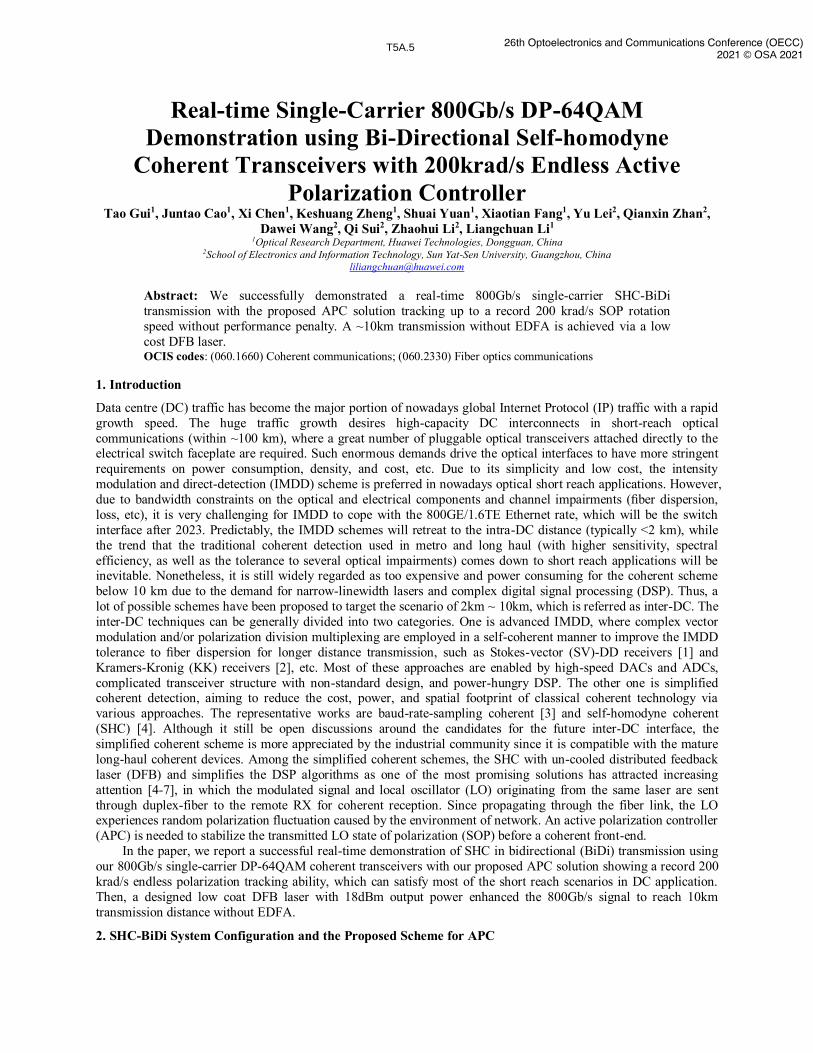
Fig. 1 (a) Structure of SHC-BiDi transmission; (b) The typical APC based on LiNbO3 multistage wave-plates with a classical ICR; (c) the
proposed APC scheme with one stage LiNbO3-based rotatable half-wave plate (HWP) and modified ICR.
We have proposed APC on an impacted SiP chip via several thermal phase shifters, tracking up to 300 rad/s without performance penalty [5]. Such tracking speed is mainly limited by the bandwidth of the thermal phase shifters (<20kHz). Besides, before the “digital coherent revolution” (over 10~20 years ago), a number of approaches [8,9] have worked on endless fast APC based on Lithium-Niobate (LiNbO3) polarization controller due to its high respond speed (100 ns). Fig. 1(b) shows a typical APC based on LiNbO3 multistage wave plates (inset a) in front of a classical ICR. Its objective is to track the random walking SOP to a horizontally polarized light (a certain point on the Poincaré sphere). Such tracking goal requires the multistage wave-plates work coordinately, thus leads to a complex control system with tracking speed limited by the “endless” requirement. Actually, the tracking goal can be simplified in SHC-BiDi that to produce equal power of LO to beat with the 2 orthogonal polarizations signals in ICR. On Poincaré sphere viewing, the target SOP is the circle of Longitude where S1=0 (shown as Fig. 1(c)). Thus, we propose to use one stage LiNbO3-based rotatable half-wave plate (HWP) together with the modified ICR as shown in Fig. 1(c). The HWP can endlessly rotate the input SOP on its Latitude circle of Poincaré sphere with a limited range of driving voltage VA and VC [9]. Thus, it can transfer any input SOP to the target Longitude ring with proper driving voltages.
3. Experimental Demonstration and Results Discussion
Fig. 2 The effectiveness of the proposed APC, showing by a) the received SOP on Poincaré sphere and b) the magnitude of error signals after
BPD as a function of time. The input SOP is under different rotation speed generated by polarization scrambler (Novoptel EPS1000) to cyclically rotate all of its internal wave-plates at different rotation speeds.
We firstly demonstrated the proposed APC via an EOSPACE polarization controller (only one stage HWP is functioned) and designed a dedicated electronic control circuit. As Fig. 2 shows, a fraction of the output lights after
the polarization rotate splitter (PSR) are tapped from the waveguide then received by the balanced photodiode (BPD) as the feedback error. This error signal is detected by an ADC as the input of the control algorithm that runs on an FPGA platform equipped with 2 output DACs, whose voltages are then applied to the HWP. Our algorithm is based on gradient descent method to minimize the errors which represented by the difference between the two power LOA and LOB. Fig. 2 shows the effectiveness of the proposed APC via the received SOP (detected by Agilent Polarimeter) on Poincaré sphere and the error signals after BPD. We can see that the APC stably locks the random rotate SOP to the large ring under 200 krad/s rotation speed. After that, the performance of APC begins to become unstable with several unlock periods (as the spikes on the error signal distribution after BPD in Fig. 2). In the future, such LiNbO3-based HWP can be integrated together with the ICR through the silicon and LiNbO3 hybrid integration platform [10], which may have much faster tracking speed due to its higher response speed and lower Vπ voltage.
Fig. 3 a) The experimental setup of SHC-BiDi system; b) Multiple-measured pre-FEC BER vs. LO SOP rotation speeds; c) Link loss margin
vs. transmission distance.
Then, we show the real-time SHC-BiDi demonstration setup as Fig. 3 (a) based on our 800 Gb/s single-carrier DP-64QAM coherent BiDi transceiver product (inset a) and the proposed APC solution. 100GE client signal from Ethernet tester is mapped over the optical signal to verify a long-term performance testing. The fiber link is setup by duplex fibers, pre-terminated optical cable, and commercial connectors (inset c) to better simulate the real link in DC. Such link can keep the mismatch distance between the signal and LO lanes within a few centimeters, minimizing the phase noise influence. A polarization scrambler is set on the LO link to emulate fast polarization variations. Firstly, the pre-FEC BER performances are measured multiple times over short periods under different LO SOP rotation speeds. As shown in Fig. 3(b), there is a negligible performance penalty up to 200 krad/s rotation. After that, the BER starts to strongly fluctuate over the time and the average performance is gradually degraded. Even sometimes, the transmission is crashed since the BER is beyond the FEC threshold. Such phenomenon are consistent well with the results in Fig. 2. Then, a long term testing based on Ethernet client reported an error-free transmission over 24 hours under 200krad/s rotation, which proves the feasibility and reliability of the proposed APC. In Fig. 3 (c), we measured the link loss margin of our real time transceiver product as a function of transmission distance in a non-EDFA link. A DFB laser with 18dBm output power and ~500 kHz linewidth is used, where a few ten MHz laser frequency dithers is applied to suppress stimulated Brillouin scattering (SBS) effect in LO path. Our experimental results demonstrated that the 800Gb/s signal can reach to ~10 km with 1.25 dB margin. Note that the insertion loss of APC is considered as ~2.5dB (measured from the EOSPACE polarization controller) which is promising to be further reduced by the thin film LiNbO3-based HWP integrated with ICR.
4. Summary
To the best of our knowledge, we have firstly demonstrated the real-time 800-Gb/s SHC-BiDi transmission with a record 200krad/s SOP tracking solution. In addition, we show a ~10km 800-Gb/s transmission in non-EDFA links. Such results indicate the potentials and feasibilities of SHC-BiDi transceivers for future high-speed inter-DC optical interconnects
5. Reference [1] T. Hoang, et al., J. Lightw. Technol., 36, 460-467, 2018. [2] A. Mecozzi, et al., Optica, 3, 1220–1227, 2016. [3] A. Gorshtein, et al., Photon. Technol. Lett., 22(16), 1208–1210, 2010. [4] M. M. Osman et al., Opt. Exp., 26(7), 8890-8903, 2018. [5] T. Gui, et al., in OFC 2020, PDP paper Th4C.3. [6] T. Gui, et al., J. Lightw. Technol. 39 (4), 1231-1238, 2021. [7] Y. J. Wen, et al., Opt. Exp., 28(15), 21940-21955, 2020. [8] R. Noé, et al., J. Lightw. Technol., 6, 1199-1208, 1988. [9] B. Koch, et al., Electron. Lett., 47(14) 813-814; 2011. [10] M. He, et al., Nat. Photonics, 13, 359-364, 2019.
Single-Lane 402 Gb/s PAM-8 IM/DD Transmission Based on a Single DAC and an O-Band Commercial EML
Md Sabbir-Bin Hossain1, 2*, Jinlong Wei1*, Fabio Pittalà1, Nebojša Stojanović1, Stefano Calabrò1, Talha Rahman1, Tom Wettlin2, Changsong Xie1, Maxim Kuschnerov1, and Stephan Pachnicke2
1 Huawei Technologies Duesseldorf GmbH, Munich Research Center, Riesstr. 25, 80992 Munich, Germany 2 Kiel University (CAU), Chair of Communications, Kaiserstr. 2, 24143 Kiel, Germany
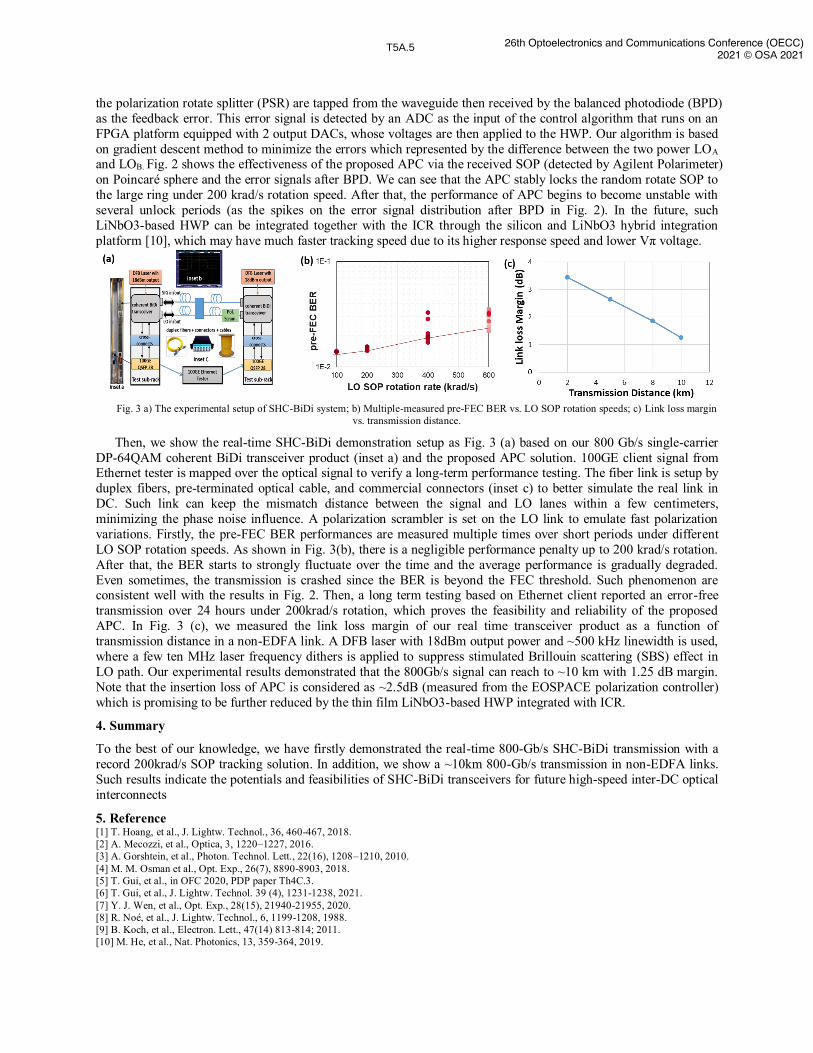
Data center networks (DCNs) account for more than 90% of the Internet traffic, which exhibits an exponential growth further reinforced in the pandemic when various cloud applications surge such as video-on-demand, gaming, and remote office work. This drives the evolution to the next generation DCN with Ethernet transceivers beyond 400 Gigabit Ethernet (GbE). Intensity modulation and direct detection (IM/DD) has been enabling a cost-effective interconnect solution to address these challenges. 200 Gb/s/lane IM/DD transmission is under specification in the 800G Pluggable MSA [1] and is under consideration for IEEE standardization [2]. Energy-efficient and high bandwidth (BW) optical components are critical technologies to increase the speed of IM/DD transmissions. So far O-band opto-electronic components have been used in standardized short-reach optical modules for links below 10 km [3-13]. O-band modulators including directly modulated lasers (DMLs) [3-5], electro-absorption modulated lasers (EMLs) [6-9] and Mach-Zehnder modulators (MZM) [10-13] have been demonstrated for short-reach IM/DD transmission links at 200+ Gb/s bit rates, as summarized in Fig. 1(a). A >100GHz DML has enabled the highest net bit rate of 321.24 Gb/s based on discrete multi-tone (DMT) signaling [3]. Due to the bandwidth limitation of the digital-to-analogue converter (DAC), a high BW RF analogue band multiplexer (MUX) was used in [3] to combine data streams from two DACs. An optical amplifier was also used in [3] to boost the receiver input power. With a similar RF MUX configuration, an EML could achieve a net bit rate of up to 266.7 Gb/s [6]. O-band MZMs [10-13] have not shown better performance compared to DMLs and EMLs. In this paper, we report record single-lane 402 Gb/s PAM-8 IM/DD transmission based on a commercially available EML at 1310.9 nm, which represents to the best of our knowledge the highest IM/DD lane rate ever achieved by using O-band optical modulators. The packaged EML, which is shown in an evaluation kit in Fig. 1(b), has a 3-dB bandwidth of 55 GHz as shown in Fig.1 (c). Considering a forward error correction (FEC) with 15.31% overhead and a threshold bit error rate (BER) of 2×10⁻² [14,15], PAM-8 transmission at a net bit rate of 348.62 Gb/s is successfully demonstrated for a transmission distance of 2 km, measuring a BER of 1.54×10⁻², well below the threshold. Compared with the previous O-band DML transmission record [3], we use a single DAC, driver-free modulation, commercial EML and optical amplifier-free receiver, enabling improved spectral and power efficiency solutions for datacom optics.
(b)(c)
(a)200
240
280
320
360
400250 300 350200
Net
bit
rate
(Gb/
s)
Gross bit rate (Gb/s)
MLO-band DMLO-band EZMMO-band
le DAC]This work, sing[
Mux][3, band
DM][5, ET [6, band Mux]
][8, single DAC[9, ETDM]
11, single DAC][
single DAC][10,C][12, single DA
ngle DAC][13, si
Mux][7, band
[4, single DAC]
Fig. 1. (a) A summary of short reach IM/DD transmissions at lane rates beyond 200 Gb/s based on O-band optical modulators, (b) the packaged
O-band EML on an evaluation kit, and (c) its normalized S21 frequency transfer function.
The experimental setup is depicted in Fig. 2. Below each electro-optical component, we report its 3-dB BW. Offline transceiver digital signal processing (DSP) is also depicted. A pseudorandom binary sequence (PRBS) is mapped to 8-level pulse amplitude modulation (PAM-8) symbols using a Gray mapping. PAM-8 with a symbol rate of 134 GBd is generated at 1 sample per symbol (sps). The quantized data is then fed to an arbitrary waveform generator (AWG) with 3-dB BW of >55 GHz and nominal sampling rate of 128 GSa/s. An external clock source set to 67 GHz is used to operate the AWG at 134 GSa/s, which is beyond the prescribed specification. A lower temperature was maintained to achieve stable operation when overclocking the AWG. Afterwards, the driver-free analog signal directly modulates an O-band EML (3-dB BW ≈55 GHz), which is biased at -3.1V for linear operation (EML transfer curve is presented in Fig. 2 (a)) whereas a 60-mA current is supplied to the integrated laser diode of the EML. During the experiments ≈ 25° C was maintained for the packaged EML. Both optical back-to-back (B2B) and 2 km standard single-mode fiber (SSMF) transmissions are measured. A variable optical attenuator (VOA) is used after the fiber link to sweep the received optical power (ROP). The optical signal is then detected and converted to an electrical signal with a 75 GHz PIN photodetector (PD). A commercial transceiver would contain a transimpedance amplifier (TIA) after PD. However, this experiment is conducted with a 22 dB fixed gain 60 GHz electrical amplifier (EA) due to absence of a TIA during the experiment. Besides, an optional inline optical power monitor is inserted between the VOA and the PD to monitor the ROP. The amplified electrical signal is then quantized and captured with a digital storage oscilloscope (DSO), which operates at 256 GSa/s with 3-dB BW set to 70 GHz. Data is captured for different values of ROP adjusting the VOA before the inline optical power monitor. 1 million samples are used for receiver-side offline processing. For estimating and compensating jitter and frequency sampling offset, timing recovery is performed [16]. After time synchronization, the signal is resampled to 1 sps and processed with a Volterra nonlinear equalizer (VNLE). A memory length of 551 taps is used for linear equalization to minimize the effect of reflections from the discrete component setup, long copper cables and connectors. In addition to linear taps, 2nd and 3rd order kernels of VNLE with memory length of 11 and 7, respectively, are used to compensate nonlinearities introduced by AWG, EML and square-law detection. To reduce post-cursor inter symbol interference (ISI), decision feedback equalization (DFE) with memory length of 2 taps is used after VNLE. This processing step is iterated twice, namely the DFE coefficients are calculated in training mode in the first iteration to set the decision threshold for the second iteration. Afterwards symbols decision is performed on the PAM-8 symbols followed by symbol to bits de-mapping and BER calculation. 3. Transmission Results and Discussions The experimental results obtained with VNLE complemented with DFE are shown in Fig. 3 and presented as BER over ROP sweep. For the B2B scenario, the BER threshold of 2×10⁻² for the considered SD-FEC is reached at 1.3
(c)(b)
(d)
Tx DSP(Offline)
AWG128 GSa/s
DSO256 GS/s
Rx DSP(Offline)
70 GHz>55 GHz
0/2 km SSMF 75 GHz
PDVOA
55 GHz
Power Monitor
DC
O-Band EML
External Clock Source
60 GHz
EA
Resampling
PAM-8 de-mapping
Computing BER
VNLE
DFE
Timing Recovery
PRBS
PAM-8 mapping
22 dB
(a)
Rx DSPTx DSP
Fig. 2: Schematic of the IM/DD transmission system with transmitter and receiver-side offline DSP. Inset (a) shows the transfer curve of the EML and the operation point indicated with a red circle. The optical spectrum of the signal for B2B and 2 km is presented in inset (b). The power spectrum density of the received signal is shown in the inset (c). Inset (d) shows the histogram of the uniformly distributed 8-level PAM transmit sequence. AWG: arbitrary waveform generator, EA: electrical amplifier, EML: electro-absorption modulated laser, VOA: variable optical attenuator, PD: photodiode, DSO: digital storage oscilloscope, VNLE: Volterra nonlinear equalization, DFE: decision feedback equalization.
dBm, and for the 2 km SSMF scenario a power penalty of -0.1 dB is observed. The negative penalty may be attributed to the compensation of the EML chirp by the residual fiber chromatic dispersion at the wavelength of 1310.9 nm. In addition, Fig.4 shows the log histogram of the equalized received symbols with different equalization configurations, where results are obtained with various numbers of taps of a linear feed-forward equalizer (FFE), 2nd and 3rd order VNLE kernels as well as the DFE. As an example, the captured data for B2B at ROP 3 dBm is used. Only using 551 linear taps for feed-forward equalization, the resultant BER (4.8×10⁻²) is not sufficient to reach the 15.31% target SD-FEC threshold. Inclusion of the 2nd and 3rd order VNLE kernels lowers the error floor up to 3.2×10⁻², which is still not sufficient to reach SD-FEC threshold. Nevertheless, a resultant BER (1.3 ×10⁻²) below the threshold of interest is achieved after including a 1 tap DFE. Moreover, further improvement is achieved with 2 tap DFE (9.7×10⁻³). DFE significantly improves the separation between neighboring levels, which can be seen in Fig. 4. However, including additional DFE taps does not bring any significant gain. 4. Conclusions We have experimentally demonstrated record transmission of PAM-8 IM/DD signal over 2 km SSMF achieving a 402 Gb/s gross bit rate, which yields a net bit rate of 348.62 Gb/s considering an SD-FEC with 15.31% overhead. To the best of our knowledge, these are the highest transmitted gross and net bit rates on a single-lane IM/DD system using a driver-free O-band EML and single DAC. The experimental setup also does not contain any optical amplifier reflecting the implementation of a future product. Acknowledgment We would like to thank Sumitomo Electric Device Innovations, Inc. for providing the packaged EML component for the experiment. References [1] 800G Pluggable MSA. Available at https://www.800gmsa.com [online] [2] IEEE 802.3 Beyond 400 Gb/s Ethernet Study Group Public Area, available at https://www.ieee802.org/3/B400G/public/index.html [online] [3] N.-P. Diamantopoulos et al., “Net 321.24-Gb/s IMDD Transmission Based on a >100-GHz Bandwidth Directly Modulated Laser,” OFC
2020, PDP Th4C.1 [4] D. Che et al., “Long-Term Reliable >200-Gb/s Directly Modulated Lasers with 800GbE-Compliant DSP,” OFC 2021, PDP F3A.3 [5] S. Yamaoka et al., “239.3-Gbit/s net rate PAM-4 transmission using directly modulated membrane lasers on high thermal conductivity SiC,”
ECOC 2019, PD2.1 [6] H. Yamazaki et al., “160-GBd (320-Gb/s) PAM4 Transmission Using 97-GHz Bandwidth Analog Multiplexer,” PTL, 30, 1749-1751 (2018). [7] H. Yamazaki et al., “300-Gbps Discrete Multi-tone Transmission Using Digital-Preprocessed Analog -Multiplexed DAC with Halved Clock
Frequency and Suppressed Image”, ECOC 2016, PDP, pp. 1-3 [8] W. Wang et al., “Demonstration of 214Gbps per lane IM/DD PAM-4 transmission using O-band 35GHz-class EML with advanced MLSE
and KP4-FEC,” OFC 2020; M4F.4. [9] S. Kanazawa et al., “Transmission of 214-Gbit/s 4-PAM signal using an ultra-broadband lumped-electrode EADFB laser module,”
OFC2016, Th5B.3 [10] J. Zhang et al., “280 Gb/s IM/DD PS-PAM-8 Transmission Over 10 km SSMF at O-band For Optical Interconnects,” OFC 2020, M4F.1 [11] M.S.B. Hossain et al., “Feasibility of Transmitting 270 Gbit/s with PAM-8 in O-band CWDM4 with IM/DD System,” OFC 2021, W7F.3 [12] A. Masuda et al., “255-Gbps PAM-8 Transmission under 20-GHz Bandwidth Limitation Using NL-MLSE Based on Volterra Filter,” OFC
2019, WI4. 6 [13] T. Rahman et al., “1.6 Tb/s Transmission Feasibility Employing IM/DD for Data Centre Networks,” ECOC 2020 pp. 1-4 [14] Open ROADM MSA. Available at http://openroadm.org/download.html [online] [15] G. Tzimpragos et al., “A Survey on FEC Codes for 100 G and beyond optical networks,” in IEEE Comm. Surv. & Tutor., vol. 18, no. 1, pp.
209-221, 2016 [16] F. M. Gardner, “A BPSK/QPSK Timing-Error Detector for Sampled Receivers,” IEEE Tran. on Comm., vol. COM-34, no. 5, pp. 423-429,
1986.
Fig. 3: Experimental results of 134 GBd PAM-8 for B2B and 2km.
Fig. 4: Histogram of the equalized received symbols for different
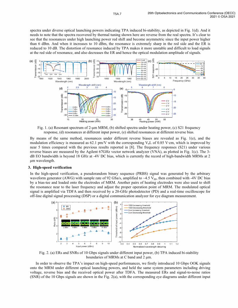
High-speed silicon micro-ring modulator at 2-μm waveband
Weihong Shen1,3, Gangqiang Zhou1,3, Jiangbing Du1,*, Linjie Zhou1, Ke Xu2, and Zuyuan He1
1State Key Laboratory of Advanced Optical Communication Systems and Networks, Shanghai Jiao Tong University, Shanghai 200240, China. 2Department of Electronic and Information Engineering, Harbin Institute of Technology (Shenzhen), Shenzhen 518055, China.
Recent years, in virtue of hollow-core fiber [1] with low loss and low latency, and thulium-doped fiber amplifier (TDFA) [2] with broadband gain, 2-μm waveband has been considered as a promising communication window, especially for the short-reach optical interconnection and capacity/latency-hungry scenarios like data centers [3-4].
Thanks to the acceptable absorption loss of silicon at 2-μm wavelength, conventional silicon-on-insulator (SOI) is still a preferred platform for 2-μm wavelength integrated devices/systems [5]. Electro-optic modulators, which play key roles in optical communication systems, are also in urgent need to be extended towards 2 μm. Till now, several silicon modulators at the 2-μm wavelength have been reported, such as high-speed Mach-Zehnder modulator (MZM) up to 80 Gbps [6-7] and micro-ring modulator (MRM) with 3-Gbps data rate [8]. However, the current modulation efficiency, bandwidth and data rates still have a long way to go, to meet the demands of high-speed 2-μm-wavelength transmission, especially for low-power-consumption MRM.
Besides, weaker two-photon absorption (TPA) [9] and stronger free-carrier dispersion (FCD) [10] at longer wavelength make it more attractive for 2-μm-wavelength silicon modulators. Particularly, when it comes to MRM, TPA effect accumulated in the resonator brings in the distortion in both the time and frequency domain, i. e. self-pulsation (SP) and optical bi-stability (BI), therefore results in deterioration of high-speed performances [11]. Weaker TPA coefficient makes 2-μm silicon MRM more tolerant to the high optical launching power, so as to achieve better high-speed performances.
In this work, we report the state-of-art high-speed silicon integrated MRM working at the 2-μm waveband. The proposed MRM presents 18-GHz electro-optic bandwidth at 4V reverse bias, and modulation efficiency of 0.85 V‧cm. Up to 50-Gbps none-return-to-zero on-off-keying (NRZ-OOK) modulation is realized with a bit error rate (BER) under 3.8e-3. TPA induced spectrum distortion is observed in the 2-μm MRM, and so is the impact on eye performances. However, 2-μm MRM shows ~3 dB higher power threshold of TPA compared with MRM in the C band, so as to achieve better high-speed performances at higher launching power. This work fills the blank space of high-speed silicon MRM at 2-μm, and also is the first time to observe and analyze the TPA effect in 2-μm MRM. It shows the promising perspective of high-speed silicon integrated circuits at the 2-μm waveband.
2. Static characterization The silicon 2-μm-wavelength MRM is designed on the 220-nm SOI wafer with 2-μm-thick buried oxide layer. The rib waveguide with 90-nm-thick slab is 600-nm wide propagating at 2 μm wavelength. The phase shifter in MRM is designed with a L-shaped PN junction in order to increase the modulation efficiency [12]. The doping concentrations are 8e17 cm−3, 1e18 cm−3, 1e20 cm−3, and 1e20 cm−3 for the n, p, n++, and p++ doping regions, respectively. The device was fabricated by MPW run in AMF, Singapore. Fiber-to-chip coupling via inverse tapers has ~5 dB/facet loss at 2 μm. A fiber laser source with a fixed single wavelength near 1960 nm and the ASE broadband source centered at 1850 nm were employed to measure the transmission spectrum of MRM. The resonant spectrum is plotted in Fig. 1(a), showing free spectrum range of 16.75 nm, full width at half maximum of 0.94 nm and the extinction ratio (ER) near 1960 nm over 15 dB.
Due to the lack of a tunable laser at 2 μm, the operation point of MRM was tuned by applying a voltage to the heater and shifting the resonance close to the laser wavelength. Thus, we mapped the resonance shift with the heating power, as shown in Fig. 1(b), abstracting the thermal tuning efficiency of 0.15 nm/mW. By using the single-frequency laser source, power meter at 2 μm, and sweeping the heating power, we obtained the resonant
spectra under diverse optical launching powers indicating TPA induced bi-stability, as depicted in Fig. 1(d). And it needs to note that the spectra recovered by thermal tuning shown here are reverse from the real spectra. It’s clear to see that the resonances under high launching power red shift and become asymmetric since the input power higher than 6 dBm. And when it increases to 10 dBm, the resonance is extremely sharp in the red side and the ER is reduced to 10 dB. The distortion of resonance induced by TPA makes it more unstable and difficult to load signals at the red side of resonance, and also decreases the ER and hence the optical modulation amplitude of signals.
Fig. 1. (a) Resonant spectrum of 2-μm MRM, (b) shifted spectra under heating power, (c) S21 frequency
response, (d) resonances at different input power, (e) shifted resonances at different reverse bias. By means of the same method, resonances under different reverse biases are revealed as Fig. 1(e), and the modulation efficiency is measured as 62.1 pm/V with the corresponding VπL of 0.85 V‧cm, which is improved by near 5 times compared with the previous results reported in [8]. The frequency responses (S21) under various reverse biases are measured by the Agilent 67GHz vector network analyzer (VNA), as plotted in Fig. 1(c). The 3-dB EO bandwidth is beyond 18 GHz at -4V DC bias, which is currently the record of high-bandwidth MRMs at 2 μm wavelength.
3. High-speed verification In the high-speed verification, a pseudorandom binary sequence (PRBS) signal was generated by the arbitrary waveform generator (AWG) with sample rate of 92 GSa/s, amplified to ~4.5 Vpp, then combined with -4V DC bias by a bias-tee and loaded onto the electrodes of MRM. Another pairs of heating electrodes were also used to shift the resonance near to the laser frequency and adjust the proper operation point of MRM. The modulated optical signal is amplified via TDFA and then received by a 20-GHz photodetector (PD) and a real-time oscilloscope for off-line digital signal processing (DSP) or a digital communication analyzer for eye diagram measurement.
Fig. 2. (a) ERs and SNRs of 10 Gbps signals under different input power, (b) TPA induced bi-stability
boundaries of MRMs at C band and 2 μm. In order to observe the TPA’s impact on high-speed performances, we firstly introduced 10 Gbps OOK signals
onto the MRM under different optical launching powers, and held the same system parameters including driving voltage, reverse bias and the received optical power after TDFA. The measured ERs and signal-to-noise ratios (SNR) of the 10 Gbps signals are shown in the Fig. 2(a), with the corresponding eye diagrams under different input
powers. The SNRs keep rising up as the launching power increases, which is straightforward that TDFA brings more noises for the lower input power. However, the ERs firstly go up along with the increased power, but reach a bottleneck and then fall down at the high launching power of 10 dBm, which can find the proof from Fig. 1(d) (the distorted resonant with lower ER at 10 dBm input). This phenomenon indicates that there exists an optimal launching power, which not only alleviates the ASE noises brought by high-gain TDFA under low input power, but also prevent the strong TPA induced ER reduction under high input power.
As for the high-speed transmission system, the higher the optimal launching power, the better the ERs and SNRs of received signals. In this case, thanks to the lower TPA coefficient, 2-μm waveband in SOI platform reflects natural advantages compared to the conventional transmission window C band. To prove this, optical bi-stability (BI) in silicon MRM induced by thermo-optical (TO) effect, TPA and other nonlinear effects is theoretically analyzed by coupled mode theory and linear stability analysis method [13]. Taking account of the higher Kerr effect, lower TPA, stronger FCD and free-carrier absorption (FCA) effect at 2 μm contrast to C band, and setting the identical parameters of MRMs in the two wavebands, we obtained the BI boundaries in the map of input power and wavelength detuning. As shown in Fig. 2(b), both the upper and lower thresholds of launching power present 3 dB higher at 2 μm than that in C band, which means the silicon MRM at 2 μm can endure much higher input power, holding high-quality high-speed transmission and keeping unaffected by TPA. These results illustrate the superior application prospects of silicon integrated circuits at 2 μm, especially for the high-speed interconnect systems with hungry power penalty.
After adjusting the operation point of MRM to get rid of TPA, eye diagrams of 20 and 30 Gbps OOK signals were observed on the sampling oscilloscope, as shown in Fig. 3(a-b), appearing clear open eyes with the ERs of 2.659 dB and 2.125 dB respectively. A higher data rate can be achieved by applying a root raised cosine filter and feed-forward equalization (FFE) at the transmitter/receiver side. The BER curves of the 40-Gbps and 50-Gbps OOK signals are plotted in Fig. 3(c). The 40-Gbps OOK signal has a BER under 7% forward error correction (FEC) threshold (3.8e-3) at >-5 dBm received optical power, and the 50-Gbps OOK signal shows a BER of 4.4e-4 at 3 dBm. The corresponding post-FFE eye diagrams are also depicted.
Fig. 3. (a-b) Eye diagrams of 20 and 30 Gbps signals, (c) BER curves of 40 and 50 Gbps signals.
4. Conclusion The state-of-art high-speed silicon micro-ring modulator working at 2-μm waveband was demonstrated with 18-GHz bandwidth, high modulation efficiency and up to 50-Gbps signaling. TPA induced spectrum distortion and deterioration of high-speed signals were observed in the 2-μm MRM. And theoretical studies reveal the higher threshold of launching power at 2-μm MRM so as to avoid TPA’s impact on high-speed transmission. Thus, silicon MRM at 2 μm waveband shows promising perspective in the high-speed optical interconnect systems.
Acknowledgement National Natural Science Foundation of China (NSFC) (61935011, 61875124, 61875049); National Key Research and Development Program of China (2018YFB1801004).
5. References [1] G. T. Jasion, et al, OFC PDP 2020, paper Th4B.4. [2] Z. Li, et al, Opt. Express 21, 26450-26455 (2013). [3] W. Shen, et al, J. Lightwave Technol. 38(15), 3874-3882 (2020). [4] W. Shen, et al, Photon. Res. 8(9), 1484-1490 (2020). [5] J. Li, et al, IEEE Photon. Technol. Lett. 30, 471–474 (2018). [6] W. Li, et al, OFC 2020, paper M1D.4. [7] X. W, ei al, Photon. Res. 9(4), 535-540 (2021). [8] W. Cao, et al, Optica 5(9), 1055-1062 (2018).
[9] A. D. Bristow, et al, Appl. Phys. Lett. 90, 191104 (2007). [10] M. Nedeljkovic, et al, IEEE Photon. J. 3, 1171-1180 (2011). [11] M. D. Cea, et al, Opt. Express 27, 24274-24285 (2019). [12] G. Zhou, et al, ICIOP 2018, 1096419. [13] L. Zhang, et al, Phys. Rev. A 87, 053805 (2013).
Field Trial of Cable Safety Protection and Road Traffic Monitoring over Operational 5G Transport Network with
Fiber Sensing and On-Premise AI Technologies Ming-Fang Huang1, Shaobo Han1, Glenn A. Wellbrock2, Tiejun J. Xia2, Chaitanya Narisetty1, Milad Salemi1, Yuheng Chen1, James M. Moore3, Philip N. Ji1, Giovanni Milione1, Ting Wang1, Yukihide Yoda 4, Yoshinori
Kitahara4, Morio Ito 4, Yoshiaki Aono4 and Atsuo Itoh 4 1NEC Laboratories America, 4 Independence Way, Princeton, NJ 08540, USA
2Verizon, 1201 E Arapaho Rd, Richardson, TX 75081, USA 3Verizon, 999 W Main St, 02 Floor, Freehold, NJ 07728, USA 4NEC Corporation, Minato-ku 108-8001, Japan
1. Introduction Over the past 30 years, telecom carriers have built large-scale fiber infrastructures to support Internet traffic growth, especially for coming 5G networks [1]. Although intended for only solo function of data transmission, it is now established that ordinary transmission fibers can be utilized as sensing media [2, 3] by using distributed fiber optic sensing (DFOS) technologies, doubling the value of carriers’ fiber assets. Emerging applications include traffic monitoring and incident detection [3, 4], pavement surface roughness level evaluation [5], seismic monitoring [6], and environmental temperature measurement [7]. Meanwhile, DFOS technologies can help locate underground fiber cables [8], identify threats to the cables [9] and thus improve the reliability of infrastructure.
In this paper, we report for the first-time the use of fiber optic sensing and machine learning technologies as a unique solution for continuous monitoring an operational 5G transport network, to both protect the cable itself and monitor the environmental surrounding activities. Over the same fiber, our intelligent sensing system processes data in real-time and extracts useful information for cable threat detection, localization, and traffic detection. The trial results provide a holistic view of the road traffic covered the entire route, which has the potential to discover seasonal variations in traffic congestion, vehicle counts, and speed. The fine-grained temporal resolution and low latency enables transportation operators to design adaptive and precise traffic management strategies, such as dynamic routing to avoid congestion or reduce accidents. Additionally, various cable threat events in the field are detected and localized, including fall-down incidents (pole, tree, or stone), road constructions, and distant vibrating sources. Reporting these events instantaneously can allow quick actions to be taken, preventing potential damage on both the sensing of communication functionalities using fiber sensing. 2. System Design for Joint Sensing of Road Traffic and Cable Threats with Real-time Processing By detecting the intensity change of Rayleigh scattering via interferometric phase beating in fiber, fiber optic sensing technology senses any vibrations near a fiber cable and generates a large volume dataset. Processing data locally with on-premise AI reduces cost in both data transmission and storage and enhances data privacy. We develop Fiber-VTMS (Vehicle Traffic Monitoring System) and Fiber-CS3 (Cable Safety Self-Protection System), hosted on an edge AI platform with high benefit-cost ratio. Fig. 1 illustrates the two-in-one system connected to single field fiber. Information sharing between Fiber-VTMS and Fiber-CS3 allows the discovery of complex correlated events and thus reducing false alarms, e.g., road construction as the root cause of traffic jams or responsible parties for a cable damage event. The GPS coordinates of detected events can be pinpointed by a cable localization module [7].
Fiber-VTMS uses a convolutional network architecture for precise segmentation of normal traffic patterns with a high-frame rate. Vehicle counts and speeds are provided by a post-processing step. Fiber-CS3 solicits online
Figure 1: Flow chart of proposed AI platform for simultaneous multipurpose sensing.
Figure 2: Field results of the long-term traffic monitoring system.
information from Fiber-VTMS and utilizes it to establish a location-specific threshold for abnormal detection over a certain time window. Strong vibration points are first detected by a saliency detector. Those points that cannot be attributed to normal traffics in Fiber-VTMS are fed into Fiber-CS3. Accordingly, dense spatial-temporal sensing data is reduced to a sparse format, such that abnormal detection can be conducted on-the-fly with low latency. The threat level of the detected abnormal event is further assessed based on time-frequency representations. The location of the detected events along the cable can be pinpointed on the map accurately. High-level summary results are stored in an event log for future analysis.
3. Field Trial Results The field trial conducted over a carrier’s 5G network in Long Beach Island (LBI), NJ, USA (Fig. 2(a)). A 19-km monitoring cable consists of aerial cable over the first 2-km and underground cable over remaining 17-km (buried at 40-60 inch depth). One distributed acoustic sensing (DAS) system was used. It was placed at a remote site and connected to the field fiber for real-time, continuous, and long-term monitoring (>7 months, since October 2020).
Figure 2(b) shows LBI’s traffic flow from April 15 to May 12, 2021. As can be seen, there was consistently heavier traffic on the southern part pf LBI as compared to the north. The monitored traffic volume over time suggests an increase in the number of visitors to LBI after April 24. This may be attributed to the relief of COVID-19 advisory restrictions in addition to warming temperature, which attracts seasonal tourists and residents. A 45 MPH vehicle speed (averaged every 1-minute, each 200-meters) on May 1st and 3rd is shown in Fig. 2(c). Vehicle speeding was observed early in the mornings. Additionally, at 6-7 km, where close to LBI’s main stores/restaurants are, lower speeds were detected, may be caused by tourists looking for parking spaces on Saturday (May 1). Monitored traffic (entering the island from NJ-72) in-bound to LBI shown in Fig. 2(d) and 2(e). Fig. 2(d) shows traffic variations over time as radial-polar visualizations, where angular slices and radial rings represent hourly segments over a 24-hour period and days, respectively. After 4-week monitoring, as expected, there is little traffic between midnight and 6 am, as people typically begin entering LBI at 7 am, with rush hours at nearly noon. Also, noticeably, in late April, more people visited LBI after 7 pm. Fig. 2(e) shows weekly traffic flow from March to May (2 weeks/month as examples). As can be seen, LBI is a seasonal tourist location, where more people visit on Fridays and Saturdays during late spring. Foreseeably, the traffic will be heavier in the summer.
Fig. 3 shows field results of the proposed cable safety protection system. Fig. 3(a) shows abnormal activities discovered (from both aerial and buried cables) and displayed on an evidence map. As an example, 8 days within a 7-month period were selected. Blue, red, and green circles represent road construction, aerial cable anomalies, and field experiments, respectively. The abnormal score of the events are denoted by the size and brightness of the circles (e.g., higher risk events are denoted by larger and darker circles). In our previous work [9], the cable threat-level was determined by a frequency-attenuation mechanism. Here, for the first time, the method was validated by field constructions—Event-b and Event-c. In the power-spectrum shown in Fig. 3(b) and 3(c), Event-b had more high frequency components (with three dangerous strikes) than Event-c, despite also comprising strong vibrations as indicated on the evidence map, which had only low frequency components. The threat assessment module assigned higher risk to Event-b than Event-c. Verified via visual inspection in the field, a machine <3-m away from the cable caused, Event-b (Fig. 3(b-i)). Event-c (Fig. 3(c-i)) was 100-m away from the cable, thus confirming the reliability of proposed schemes. Fig. 3(d) shows an incident where a falling pole fell directly on the monitoring cable (Event-d), which was caused by a construction accident at 2:30:21 pm on May 4.
Figure 3: Field results of detected abnormal events and experimental results on source-to-cable distance prediction.
Abnormal scores on the map indicate high risk events, which may cut or damage the cable. With fiber optic sensing technology, such events can be reported to the carrier immediately. Thus communication network downtimes can be prevented/reduced. Event-g and h were asphalt paving machines active at 8-m away, parallel to the cable. They were detected and assessed as low risk events. Additional event information such as working hours and locations were also provided. A pilot study on estimating the source-to-cable distance was successfully conducted (Event-e). Fig. 3(f-i) presents the field experimental setup. A vibrator was used to emulate machine engine noise at 1.8 to 11 m from the cable at a 0.9 m interval. The active sensing coverage was about 65.2 m along the cable. Fig. 3(e) shows the intensities of each sensing point along the cable (a total of 41 points), perpendicular from the buried cable at the midpoint (point 21). Intensities of the sensing points vary with a clearly symmetric pattern. This is expected via the physical setup of the experiment, where the intensity at the midpoint was consistently higher (brighter areas) and reduced proportionately at sensing points (darker areas) that were further away. A probabilistic model based on the estimated joint probability distribution of distance and intensities was developed. Fig. 3(f) shows the performance of the model in predicting test data distances. The mean and median indicators along with the narrow height of the boxes, demonstrate high accuracy of predictions at most distances from the cable.
4. Conclusions We have successfully demonstrated joint cable safety self-protection, event localization, and traffic monitoring applications using one DAS with one standard communication fiber in an operational 5G transport network. The continuous monitoring system dealt with variations caused by various environmental factors (e.g., weather and ground conditions) based on self-normalization. The on-premise AI platform yields low-latency so that timely actions can be taken. Fiber sensing provides a unique solution for cable safety self-protection without need of introducing other sensors, which will be very useful in supporting other mission-critical 5G and beyond applications. The field trial results show that distributed fiber sensing with AI technologies can create additional values for both carriers and third-party customers (such as transportation operators) with mutual benefits, which have great potential for future smart transportation, safer city, and smart city applications.
Acknowledgements The authors would like to thank Jason Cascio and Christoph Winkelmann from Verizon for their support to this work.
References [1] Fierce Telecom, From AT&T to Fatbeam: The top 10 (and
more) biggest providers of fiber in the U.S., 2015. [2] G. Wellbrock et al., OFC 2019, Th4C.7. [3] C. Narisetty et al., TRB, 2675(2), 233, 2021. [4] T Li et al., OFC 2021, Th1A.26.
[5] M.-F. Huang et al., JLT, 38(1), 75, 2020. [6] M. R. Fernández-Ruiz et al., APL Photonics 5, 030901, 2020. [7] G. Wellbrock et al., ECOC 2020, Th2H-1. [8] TJ Xia et al., OFC 2020, Th3A.5. [9] TJ Xia et al., OFC 2021, Th4H.3.
Over 60GHz InP CDM and ICR Enabling 800Gbps LR/ER/ZR/ZR+ Transmission Links
With 120Gbaud/DP-16QAM Modulation
You-Wei Chen*, Konstantin Kuzmin, Maxime Poirier, Tadatoshi Tomimoto, George Zarris, Ron Moore, Chengkun Chen, Wuchun Wu, Jun Huang, Marcel Boudreau, Hui Xu, and Winston I. Way
NeoPhotonics, 3081 Zanker Road, San Jose, CA 95134, USA * [email protected]
1. Introduction Despite the fact that 90-96Gbaud based 800Gb/s per wavelength line-cards have been deployed in the field since 2020, the industry is marching toward 120-130Gbaud based 800Gb/s per wavelength line-cards and pluggable modules for longer transmission distances in metro and data-center interconnection (DCI), and a high link loss budget for unamplified grey links [1]. For a coherent transmission system with ≥120Gbaud and ≥800Gb/s net data rate, all optoelectronic components must have sufficiently high bandwidths. Today, a number of ≥800Gb/s per wavelength coherent transmission experiments have been reported by using practical lithium niobate, silicon photonic (SiP), or indium phosphide (InP) polarization-multiplexed quadrature (PMQ) modulators. However, due to the limited bandwidth of the former two types, most experimental studies need to resort to sophisticated compensation methods such as optical equalization [2-5], heavy-duty linear [2,4,5] and nonlinear equalization [5], and a strong forward error correction (FEC) with a ≥20% overhead [2-5]. SiP PMQ modulators would suffer additional penalty from a high VS, and therefore no transmission distance has been demonstrated [5]. In addition, none of these experiments have used a coherent receiver with trans-impedance amplifiers (TIAs) and relied on an EDFA to boost the received optical power, thus forbid the unamplified LR/ER applications. InP PMQ modulators, however, have demonstrated a much higher bandwidths. In [6], an InP single-polarization IQ modulator with an 80GHz 6dB bandwidth was used to run a 168Gbaud/DP-16QAM experiment, using a test equipment-level coherent receiver without TIA. In [7], a subassembly of InP photonic IC and SiGe ASIC were shown to exhibit an over 50GHz 3dB bandwidth for both transmitter and receiver, and was used in a 95.6Gbaud 10u100km Raman-amplifier-based experiment with a 20% FEC overhead [8]. In this paper, we report near-term feasible 120Gbaud-based 800Gb/s LR/ER/ZR/ZR+ links by using practical InP CDM and ICR having 3dB bandwidths over 60GHz, and 400ZR-like simple off-line digital signal processing [9]. Our CDM having a high output power together with an ICR having a high sensitivity and a wide dynamic range are shown to enable a record unamplified LR (10km) and ER+ (50km) link budget at a d15% FEC overhead, and a superior OSNR performance in amplified ZR and ZR+ links at a 15% FEC overhead.
2. High-Bandwidth (HB) CDM and ICR Characteristics
Fig. 1 Frequency responses of (a) HB-CDM and (b) HB-ICR with EVB and cables de-embedded.
The InP high bandwidth (HB)-CDM shown in Fig.1(a) consists of an open collector 90nm node SiGe linear quad-driver and a PMQ modulator with a differential RF electrical termination. The chip is packaged with a surface mount technology (SMT) RF interface, compliant to the Optical Internetworking Forum (OIF) CDM implementation agreement [10] with 4 GSSG channels on a 0.8mm pitch. The frequency response of the CDM without the high frequency loss due to evaluation board (EVB) and connecting cables is shown in Fig.1(a), which exhibits a 3dB bandwidth of 61 GHz. However, the EVB and cables cause additional 5.5 and 9.5dB loss at 50 and 60GHz, respectively. The package’s dimension is 24.8 u 12 u 4.8mm3. The HB-CDM has a VS < 2.0 Volts, fiber-to-fiber insertion loss per polarization <12dB, and child and parent interferometer extinction ratios >25 dB. The InP HB-ICR in Fig.1(b) consists of a waveguide-balanced-photodetector (WG-BPD) chip, two 90nm node SiGe dual-TIA chips, and a silica-on-silicon planar lightwave circuit (PLC) chip, which integrates dual polarization optical hybrids, monitor-PD taps, and variable optical attenuators. The WG-PD chip comprises a spot-size converter (SSC), a vertical coupler, and an InP/InGaAs detector. Fig.1(b) shows the measured HB-ICR 3dB bandwidths of 64 GHz without the loss of EVB and connecting cables, whereas the EVB and cables cause additional 3 and 3.5dB loss at 50 and 60GHz, respectively. The HB-ICR has a high responsivity performance of 0.05A/W and 0.058A/W for signal and local oscillator, respectively, and a superior input referred noise spectral density of 20-25pA/�Hz across an input power range of -20 to 0dBm.
3. Experimental Setup and Results Fig. 2 shows the experimental setup. Two external cavity tunable lasers (ECTL) with a 50KHz linewidth and an
output power of +15.2 and +12.3dBm, respectively, were used to mimic the transmitter (TX) and local oscillator (LO) laser power split from a single +17.5dBm laser in an 800G pluggable module. This split ratio of 2:1 between TX and LO power was experimentally proven to maximize the LR and ER link budgets. The TX output power after HB-CDM modulation, which corresponds to the optimum linear driving swing voltage and back-to-back bit-error-ratio (BER), is -4.7 and -8.4dBm, before and after pre-equalization, respectively. The four 120Gbaud PAM4 signals (with a pattern length of 215 symbols) were generated from four DACs (each with a 65GHz 3dB analog bandwidth and an ENOB >5.5 up to 60GHz) in an arbitrary waveform generator (AWG). The sampling rate was 120GSa/s (1 sample per symbol) and no pulse shaping was applied. A frequency-domain pre-equalizer was used to pre-compensate the combined bandwidth of DAC, CDM, EVB, and RF cables. In Fig.2, the upper path for LR/ER link contains a 10 or 50km fiber spool and a variable attenuator (VOA), the lower path for ZR/ZR+ contains 100/600km fiber spools with in-line EDFAs. After the HB-ICR, the waveforms of the 120Gbaud/DP-16QAM coherent signals were recorded by a 4-channel, 110-GHz, 256GSa/s real-time scope.
To increase the TX output power for ZR and ZR+ links, we have also tested the feasibility of using a post-modulation semiconductor optical amplifier (SOA). The SOA has a noise figure of <6dB, a linear gain of 12.7dB, and a total power consumption <0.4W. Test results of the 800LR/ER link performance are described below. Fig.3(a) shows the BER versus received optical power (ROP) over LR and ER distances. At a CFEC BER threshold of 1.25e-2, the receiver sensitivities under
Fig. 2 Experimental setup for LR/ER (upper path) and ZR/ZR+ (lower path). IQM: IQ modulator
Fig.3 (a) BER vs ROP over LR/ER distances with CDM output power of -6.3 dBm. (b) Minimum required ROP and the total link budget as a function of the transmitter output power (Ptx) under different FEC BER threshold.
different cases (including back-to-back (BtB), 10 and 50km) are all around -20dBm for dual-polarizations, and <0.3dB penalties were introduced by the 50km fiber dispersion. In order to test the 800LR/ER receiver dynamic range, we also increased the ROP up to 0dBm (which required an EDFA specifically for this purpose), and found insignificant BER change. Fig.3(b) shows that a maximum link budget of 13.6dB can be achieved when the HB-CDM output power was at -6.3dBm, at which the HB-CDM was driven slightly into the nonlinear region. This link budget is sufficient to cover practical ER links [12]. For an 800LR link, the pre-FEC BER threshold is expected to be reduced to 4e-3 due to a low-latency FEC [11], the maximum link budget of 9dB was achieved when the TX output power is -7.4dBm, and the required ROP (rROP) was -16.4dBm. This link budget is 1dB higher than the target 800LR spec in OIF [1]. Next we discuss the 800ZR/ZR+ link performance. Fig.(4) shows the measured BER versus OSNR curves. The BtB rOSNR at a CFEC threshold is found to be 26.3dB. After 600km (=50km u8+100km u2) SMF transmission with EDFAs and a 0dBm/channel launched power per fiber span, the rOSNR is increased to 27dB. The link-delivered OSNR after 600km is 28.3dB, and thus the system margin is 28.3-27=1.3dB. The constellation diagrams of the 120Gbaud/DP-16QAM signal for BtB and after 600km transmission are shown in Fig.4. The TX output power may need to be increased to ~ 0dBm to match with brown-field DWDM TX output power in a ZR+ link. On the other hand, the TX output power is a main concern for a single-span 800ZR link with optical line protection [1], which could have an optical loss of d12.5dB (due to patch panels, connecting cables, a DWDM multiplexer, and a 1u2 optical splitter) before a booster EDFA. This d12.5dB loss severely limits the achievable OSNR due to the booster amplifier. Therefore, to increase the TX output power for both 800ZR and 800ZR+ links, we have tested a low-power (<0.4W) polarization-dependent post-modulation SOA. This SOA can be monolithically integrated in each X- and Y-polarization output arm of an InP PMQ, or can be co-packaged with a SiP PMQ, as shown in Fig.2. Experimentally, the SOA was placed after the HB-CDM, a VOA, and a polarization controller for testing ZR and ZR+ links. We set the input power to the SOA as -16dBm and obtain an output power of -3.3dBm, which gives a total TX output power of -0.3dBm when combining the two polarizations. This -0.3dBm TX output power can significantly improve the OSNR due to the booster amplifier to about 40dB, even with a 12.5dB loss between a TX and a booster EDFA. In the meantime, the OSNR contributed by the SOA is maintained at ≥36dB. As a result, a single-span 800ZR link can accommodate optical line protection and provide a fiber loss budget of >20dB. Fig.4(b) demonstrates that, by comparing the single-polarization (SP) results with and without SOA, there is a negligible OSNR penalty due to SOA. 4. Conclusions By using over 60GHz bandwidth InP HB-CDM and HB-ICR, we have experimentally demonstrated for the first time 800LR/ER/ZR/ZR+ transmission systems based on 120Gbaud/DP-16QAM. The record 800LR/ER link budgets are shown to be 13.6 and 9dB in using CFEC and a low-latency FEC [11], respectively. The former exceeds the unamplified 400ZR link budget [12] by 2.6dB, while the latter exceeds the target link budget [1] by 1dB. In these unamplified links, a superior 800Gb/s receiver dynamic range of > 20dB is achieved. For 800ZR+, a rOSNR of 27dB is achieved after a 600km EDFA-based transmission system. We have also demonstrated that the use of low-power SOAs can significantly improve the TX output power to ~ 0dBm in 800ZR and ZR+ links. This can enable an 800ZR DCI link with optical line protection and a fiber loss budget of >20dB. 5. References [1] www.oiforum.com/technical-work/hot-topics/800g-coherent [8] H. Sun, et al., J. Lightwave Technol., vol.38, p.4744, 2020. [2] A. Matsushita, et al., J. Lightwave Technol., vol.38, p.2905, 2020. [9] W. Jiang, et al., Photo. Technol. Lett., vol.30, p.1671, 2018. [3] F. Buchali, et al., Paper Mo1E.4, ECOC 2020. [10] OIF-HB-CDM-01.0 IA, Nov. 30, 2018. [4] J. Zhang, et al., Paper Tu2E.5, OFC 2017. [11] https://ieee802.org/3/ad_hoc/ngrates/public/calls/20_0727 [5] S. Zhalehpour, et al., Paper W3D.6, OFC2020. /lam_nea_01_200727.pdf [6] F. Hamaoka, et al., Paper Tu3B.1, ECOC2019. [12] OIF-400ZR-01.0 IA, Mar. 10, 2020. [7] V. Lal, et al., Paper M3A.2, OFC2020.
Fig.4 (a) BER vs OSNR with in-line EDFAs; (b) BER vs OSNR with (single-polarization) and without SOA. When using an SOA in TX, the PMQ output power per polarization was attenuated to -16dBm
Erbium-doped waveguide amplifier on lithium niobate on insulator with 27.94 dB total gain and 6.20 dB/cm net gain
Minglu Cai, Kan Wu*, Junmin Xiang, and Jianping Chen State Key Laboratory of Advanced Optical Communication Systems and Networks, Shanghai Jiao Tong University, Shanghai 200240, China
Lithium niobate on insulator (LNOI) or thin-film lithium niobate has attracted great attention due to its excellent performance in electro-optic modulation, microresonator and supercontinuum generation enabled by its abundant photonic properties and good mode confinement [1]. To achieve a fully integrated photonic system on LNOI, there is another key requirement, that is, the gain. Recently, erbium-doped LNOI (Er:LNOI) wafer has been successfully fabricated with ion-cutting technology. Lasers and waveguide amplifiers based on Er:LNOI are reported [2-8]. Very importantly, different from many reported erbium based integrated amplifiers with extremely high gain per unit length but very small total gain (also known as signal enhancement), Er:LNOI can simultaneously support high total gain and moderate saturation power as well as high gain per unit length. Here the total gain is defined as the power ratio of the output signal when the pump power is turned on and turned off. The internal net gain is total gain subtracting waveguide loss. Both internal net gain and total gain decrease with the increase of input signal power. The saturation power is defined as the internal net gain reaches 0 dB where the input signal power equals to the output signal power.
In this paper, we demonstrate an efficient 2.58-cm long erbium-doped waveguide amplifier on LNOI platform. The amplifier has 27.94 dB total gain (signal enhancement), 15.99 dB internal net gain, 6.20 dB/cm net gain, -8.84 dBm saturation power and 3.48 dB noise figure at 1531.6 nm. As shown in the comparison with other Er:LNOI works in Fig. 1(a), benefited from optimized waveguide design and 1484-nm pump, our work has achieved superior performance in two key specifications of total gain and saturation power. This work paves the way towards a fully integrated photonic circuits on LNOI platform and can benefit the applications including integrated optical computing, quantum computing and optical communications.
The fabrication procedures of the monolithically integrated Er:LNOI amplifier are briefly explained as follows. Firstly, the high-quality Er:LNOI (~1 mol%, Z-cut) wafer was prepared by “ion-cutting” technology. The analysis of element distribution in 200 nm depth from the wafer surface was performed by Ion Time-of-Flight Secondary Ion Mass Spectrometer (TOF-SIMS). As shown in Fig. 1(b), within the depth of 200 nm, the erbium ions uniformly distribute along the depth, which lays the foundation for the high-performance waveguide amplifier. Then a hard mask of chromium (Cr) was patterned with hydrogen silsequioxane (HSQ) photo resist, electron beam lithography (EBL) and standard dry etching process. The Cr pattern was then transferred to the Er:LNOI layer with optimized inductively coupled plasma-reactive ion etching (ICP-RIE) technology. The total waveguide height is 600 nm with a ridge height of 410 nm and a slab height of 190 nm. The top width of the waveguide is 1.4 μm and single TE mode is supported. As the pump mode at 1484 nm has a better mode overlap with 1530-nm mode than that at 980 nm, we mainly focus on the 1484-nm pump in this work for a better amplifier performance.
Fig. 1. (a) Comparison of recent works on Er:LNOI amplifiers. (b) Element distribution of Er:LNOI in 200-nm depth from the surface.
0 10 20 30 40 50 60 70
5
10
15
20
25
30
Sign
al E
nhan
cem
ent (
dB)
Pump power (mw)
(17.34,27.94),2.58cm1531.6nm/1484nm[our work]
(45,22.2),2.97cm1531.6nm/980nm[our work]
(40,18.576),3.6cm1530nm/980nm[2]
(21,6.2),5mm1531.6nm/980nm[3]
(10.78,11.94),5.3mm1531.6nm/980nm[4]
(64,15.415),5mm1531.5nm/980nm[5]
[2] J. Zhou, et al, 2021[3] Z. Chen, et al, 2021[4] X. Yan, et al, 2021[5] Q. Luo, et al, 2021
The experimental setup of Er:LNOI amplifier is shown in Fig. 2. The signal light is from a C-band tunable laser and the pump is from a homemade 1484 nm Raman laser. For forward pumping scheme, the signal and pump are combined by a wavelength division multiplexing (WDM), propagate through a polarization controller (PC) and couple to the Er:LNOI chip via a lensed fiber. The output from the chip is collected by a second lensed fiber and then propagates through a second WDM. The residual pump is extracted by the WDM and the signal is detected by an optical spectrum analyzer (OSA). For bi-directional pumping scheme, the 1484 nm pump is split by a 50:50 coupler. Half of the pump is fed to the first WDM and half to the second WDM. The inset in Fig. 2 shows a micrograph of the chip and waveguide when the pump is applied. The luminous region is the spiral waveguide amplifier on the chip.
Fig. 2. Experimental setup of integrated Er:LNOI amplifier. Inset: Micrograph of the chip with pump applied.
For forward pumping, Fig. 3(a) summarizes the wavelength dependent total gain for four Er:LNOI amplifiers with lengths of 1.38 cm, 1.94 cm, 2.58 cm, respectively. The input signal power and pump power are fixed to 3 μW and 12.54 mW, respectively. It can be observed that the total gain increases with the increasing length of the amplifiers, and the gain peaks appear around the bands of 1530 nm and 1545 nm. To estimate the internal net gain from the input to the output of the waveguide amplifiers, the waveguide loss including propagation loss and erbium absorption should be calibrated. Fig. 3(b) shows the photoluminescence (PL) spectrum of Er:LNOI (blue line). Based on the PL spectrum, the wavelength related absorption cross section can be derived, and then the absorption loss can be obtained (green line in Fig. 3(b)) [9]. The absorption cross sections at 1531.6 nm and 1550.0 nm are 1.046×10⁻²⁰ cm2 and 0.325×10-
20 cm2, corresponding to the absorption loss of 2.98 dB/cm and 0.95 dB/cm. The total loss is shown in purple line by truncation method in Fig. 3(b), and the value is 4.63 dB/cm and 3.08 dB/cm at 1531.6 nm and 1550 nm, respectively, which has been calibrated by resonator Q-analysis method. The propagation loss is therefore ~2 dB/cm.
Fig. 3. (a) Measured total gain (signal enhancement) of forward pumped Er:LNOI waveguide amplifiers with length of 1.38 cm, 1.94 cm and 2.58 cm. (b) PL spectrum of Er:LONI wafer (blue), absorption induced waveguides loss (green) and total waveguide loss (purple).
Noting that 2.35-cm-long waveguide has highest signal enhancement in the forward pumping scheme, bi-directional pumping is applied to this waveguide to further improve the gain performance. Fig. 4 shows the measured signal enhancement and internal net gain at 1531.6 nm and 1550.0 nm. At 1531.6 nm, the maximal signal enhancement is 27.94 dB for a input signal power of -50 dBm (10 nW), corresponding to the internal net gain of 15.99 dB and a net gain per unit length of 6.20 dB/cm. With the increase of input signal power, the signal enhancement and internal net gain decrease. When the internal net gain reaches 0 dB, the saturation power is -8.84 dBm. At 1550.0 nm, the gain
performance is weaker than that at 1531.6nm. The maximal signal enhancement is 10.61 dB, the maximal internal net gain is 2.66 dB, and the saturation input-signal power is -22.47 dBm.
Fig. 4. Measured signal enhancement and internal net gain of bi-directional pumped 2.58-cm waveguide at (a) 1531.6 nm and (b) 1550.0 nm. Insets: Optical spectra of input and output signal at maximal signal enhancement.
Fig. 5(a) summarizes the relation between input signal power and output signal power at 1531.6 nm and 1550.0 nm. Besides, we have measured noise figure as a function of the signal input power by the polarization extinction method [10], as shown in Fig. 5(b). The noise figure has positive correlation with the signal input power. When the signal input power is -50.39 dBm, the noise figure is 3.48 dB. For the input signal power below -20 dBm, the noise figure is less than 7 dB.
Fig. 5. (a) Signal output power and (b) noise figure versus signal input power for 2.58-cm waveguide.
In conclusion, an efficient Er:LNOI waveguide amplifier has been demonstrated with a maximal total gain of 27.94 dB total gain, a maximal internal net gain of 15.99 dB, a maximal net gain per unit length of 6.20 dB/cm and a saturation power of -8.84 dBm at 1531.6 nm. This work is a solid step towards a fully integrated photonic circuits based on LNOI platform and will have wide applications in optical / quantum computing and signal processing.
[1] D. Zhu, et al. . “Integrated photonics on thin-film lithium niobate”. Adv. Opt. Photon., 13, 242-352 (2021). [2] J. Zhou, et al., "On-chip integrated waveguide amplifiers on Erbium-doped thin film lithium niobate on insulator," arXiv:2101.00783 (2021). [3] Z. Chen, C. Wang, et al., "Efficient erbium-doped thin-film lithium niobate waveguide amplifiers," Opt. Lett. 46, 1161-1164 (2021). [4] X. Yan, et al., "Integrated spiral waveguide amplifiers on erbium-doped thin-film lithium niobate," arXiv:2105.00214 (2021). [5] Q. Luo, et al, "On-chip erbium-doped lithium niobate waveguide amplifiers," Chin. Opt. Lett., 19, 060008 (2021). [6] Z. Wang, et al., "On-chip tunable microdisk laser fabricated on Er3+-doped lithium niobate on insulator," Opt. Lett. 46, 380-383 (2021). [7] Y. Liu, X. Chen, et al., "On-chip erbium-doped lithium niobate microcavity laser," Sci. China Phys. Mech. Astron. 64, 234262 (2021). [8] Q. Luo, et al., "Microdisk lasers on an erbium-doped lithium-niobite chip," Sci. China Phys. Mech. Astron. 64, 234263 (2021). [9] M. Ohashi, "Design considerations for an Er3+-doped fiber amplifier," J. Lightwave Technol., 9, 1099, (1991). [10] M. Movassaghi, et al., "Noise figure of erbium-doped fiber amplifiers in saturated operation," J. Lightwave Technol., 16, 812, (1998).