Rev. 0 Document Feedback Information furnished by Analog Devices is believed to be accurate and reliable. However, no responsibility is assumed by Analog Devices for its use, nor for any infringements of patents or other rights of third parties that may result from its use. Specifications subject to change without notice. No license is granted by implication or otherwise under any patent or patent rights of Analog Devices. Trademarks and registered trademarks are the property of their respective owners.
FEATURES Conversion gain: 11 dB (typical) at IFOUT = 100 MHz Image rejection: 25 dB (typical) at IFOUT = 100 MHz LO to RF isolation: 46 dB (typical) LO to IF isolation: 26 dB (typical) IF output frequency: dc to 3.5 GHz 32-lead, 4.9 mm × 4.9 mm ceramic leadless chip carrier
APPLICATIONS Point to point radios Point to multipoint radios and very small aperture terminals
(VSATs) Test equipment and sensors Military end use
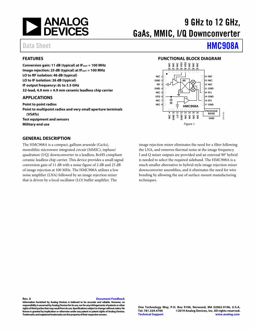
FUNCTIONAL BLOCK DIAGRAM
2GND3RF4GND5NIC6VD37NIC8NIC
1NIC
17 GND18 IF219 GND20 IF121 GND22 NIC23 NIC24 NIC
25
NIC
26
NIC
27
NIC
28
VD2
29
VD1
30
NIC
31
NIC
32
NIC
9
NIC
10
GN
D
11
LO
12
GN
D
13
NIC
14
NIC
15
NIC
16
NIC
PACKAGEBASE
GND
–90
0
2007
0-00
1
HMC908A
Figure 1.
GENERAL DESCRIPTION The HMC908A is a compact, gallium arsenide (GaAs), monolithic microwave integrated circuit (MMIC), inphase/ quadrature (I/Q) downconverter in a leadless, RoHS compliant ceramic leadless chip carrier. This device provides a small signal conversion gain of 11 dB with a noise figure of 2 dB and 25 dB of image rejection at 100 MHz. The HMC908A utilizes a low noise amplifier (LNA) followed by an image rejection mixer that is driven by a local oscillator (LO) buffer amplifier. The
image rejection mixer eliminates the need for a filter following the LNA, and removes thermal noise at the image frequency. I and Q mixer outputs are provided and an external 90° hybrid is needed to select the required sideband. The HMC908A is a much smaller alternative to hybrid style image rejection mixer downconverter assemblies, and it eliminates the need for wire bonding by allowing the use of surface-mount manufacturing techniques.
Pin Configuration and Function Descriptions ............................. 5 Interface Schematics..................................................................... 5
Theory of Operation ...................................................................... 22 LO Driver Amplifier .................................................................. 22 Mixer ............................................................................................ 22 LNA .............................................................................................. 22
Applications Information .............................................................. 23 Layout .......................................................................................... 23 Performance at Lower IF Frequencies ..................................... 25
SPECIFICATIONS TA = 25°C, LO drive level = 0 dBm, VD1 = VD2 = 3 V, VD3 = 5 V. All measurements performed on the evaluation printed circuit board (PCB).
Table 1. Parameter Test Conditions/Comments Min Typ Max Unit FREQUENCY
Radio Frequency (RF) 9 12 GHz Intermediate Frequency (IF) Output DC 3.5 GHz LO Input 8.5 15.5 GHz
LO DRIVE LEVEL −4 0 +6 dBm RF PERFORMANCE
Downconverter (IFOUT), IFOUT = 100 MHz Upper sideband Conversion Gain 8 11 dB Image Rejection 15 25 dB Input Third-Order Intercept (IP3) −3 0 dBm Input Second-Order Intercept (IP2) 31 Input 1 dB Compression Point (P1dB) −8 dBm Noise Figure 2 3.5 dB
Downconverter (IFOUT), IFOUT = 3500 MHz Lower sideband Conversion Gain 7 9 dB Image Rejection 18 30 dB Input IP3 −3 +1 dBm Input IP2 27 Input P1dB −9 dBm Noise Figure 3 dB
Amplitude Balance Taken without external 90° hybrid ±1 dB Phase Balance Taken without external 90° hybrid ±6 Degrees Isolation Taken without external 90° hybrid
LO to RF 36 46 dB LO to IF 17 26 dB RF to IF 5 dB
Return Loss Taken without external 90° hybrid LO 12 dB RF 18 dB IF1 12 dB IF2 10 dB
SUPPLIES Supply Current of RF LNA (ID1 + ID2) VD1 = VD2 = 3 V 53 85 mA Supply Current of LO Amplifier (ID3) VD3 = 5 V 100 125 mA
ABSOLUTE MAXIMUM RATINGS Table 2 Parameter Rating RF Input Power 5 dBm IFx Input Power (LO = 10 dBm, RF = −10 dBm) 15.5 dBm LO Input Power 20 dBm VD1, VD2 4.0 V VD3 5.5 V IFx Source or Sink Current 5 mA Maximum Junction Temperature (TJ) 175°C Lifetime at Maximum TJ >1 × 10⁶ hours Continuous Power Dissipation, PDISS
1 (TA = 85°C, Derate 9.56 mW/°C Above 85°C)
0.65 W
Operating Temperature Range −40°C to +85°C Storage Temperature Range −65°C to +150°C Lead Temperature (Soldering 60 sec) 260°C Moisture Sensitivity Level (MSL)2 MSL3 Electrostatic Discharge (ESD) Sensitivity
Human Body Model (HBM) 250V Field Induced Charged Device Model
(FICDM) 1250V
1 PDISS is a theoretical number calculated by (TJ − 85°C)/θJC. 2 Based on IPC/JEDEC J-STD-20 MSL classifications.
Stresses at or above those listed under Absolute Maximum Ratings may cause permanent damage to the product. This is a stress rating only; functional operation of the product at these or any other conditions above those indicated in the operational section of this specification is not implied. Operation beyond the maximum operating conditions for extended periods may affect product reliability.
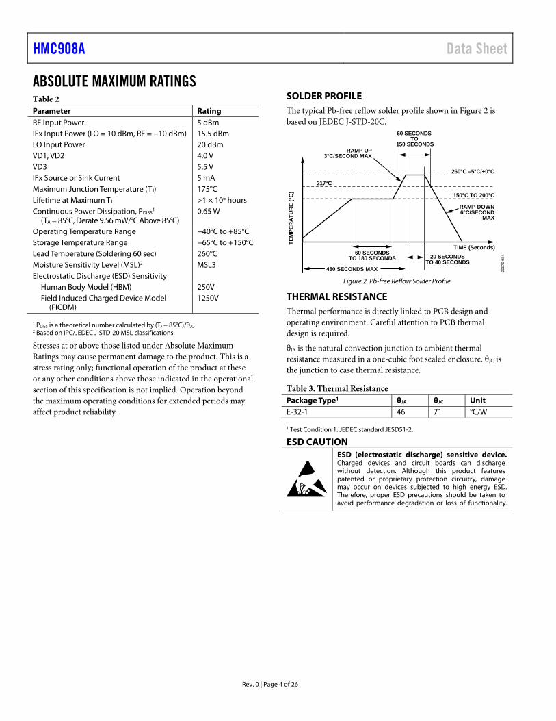
SOLDER PROFILE The typical Pb-free reflow solder profile shown in Figure 2 is based on JEDEC J-STD-20C.
60 SECONDSTO 180 SECONDS 20 SECONDS
TO 40 SECONDS480 SECONDS MAX
TEM
PER
ATU
RE
(°C
)
TIME (Seconds)
260°C –5°C/+0°C
150°C TO 200°C
RAMP DOWN6°C/SECOND
MAX
217°C
RAMP UP3°C/SECOND MAX
60 SECONDSTO
150 SECONDS
2007
0-08
4
Figure 2. Pb-free Reflow Solder Profile
THERMAL RESISTANCE Thermal performance is directly linked to PCB design and operating environment. Careful attention to PCB thermal design is required.
θJA is the natural convection junction to ambient thermal resistance measured in a one-cubic foot sealed enclosure. θJC is the junction to case thermal resistance.
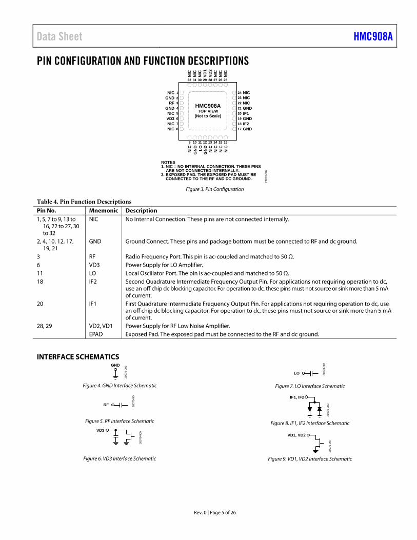
NOTES1. NIC = NO INTERNAL CONNECTION. THESE PINS ARE NOT CONNECTED INTERNALLY.2. EXPOSED PAD. THE EXPOSED PAD MUST BE
CONNECTED TO THE RF AND DC GROUND.
2007
0-00
2
Figure 3. Pin Configuration
Table 4. Pin Function Descriptions Pin No. Mnemonic Description 1, 5, 7 to 9, 13 to
16, 22 to 27, 30 to 32
NIC No Internal Connection. These pins are not connected internally.
2, 4, 10, 12, 17, 19, 21
GND Ground Connect. These pins and package bottom must be connected to RF and dc ground.
3 RF Radio Frequency Port. This pin is ac-coupled and matched to 50 Ω. 6 VD3 Power Supply for LO Amplifier. 11 LO Local Oscillator Port. The pin is ac-coupled and matched to 50 Ω. 18 IF2 Second Quadrature Intermediate Frequency Output Pin. For applications not requiring operation to dc,
use an off chip dc blocking capacitor. For operation to dc, these pins must not source or sink more than 5 mA of current.
20 IF1 First Quadrature Intermediate Frequency Output Pin. For applications not requiring operation to dc, use an off chip dc blocking capacitor. For operation to dc, these pins must not source or sink more than 5 mA of current.
28, 29 VD2, VD1 Power Supply for RF Low Noise Amplifier. EPAD Exposed Pad. The exposed pad must be connected to the RF and dc ground.
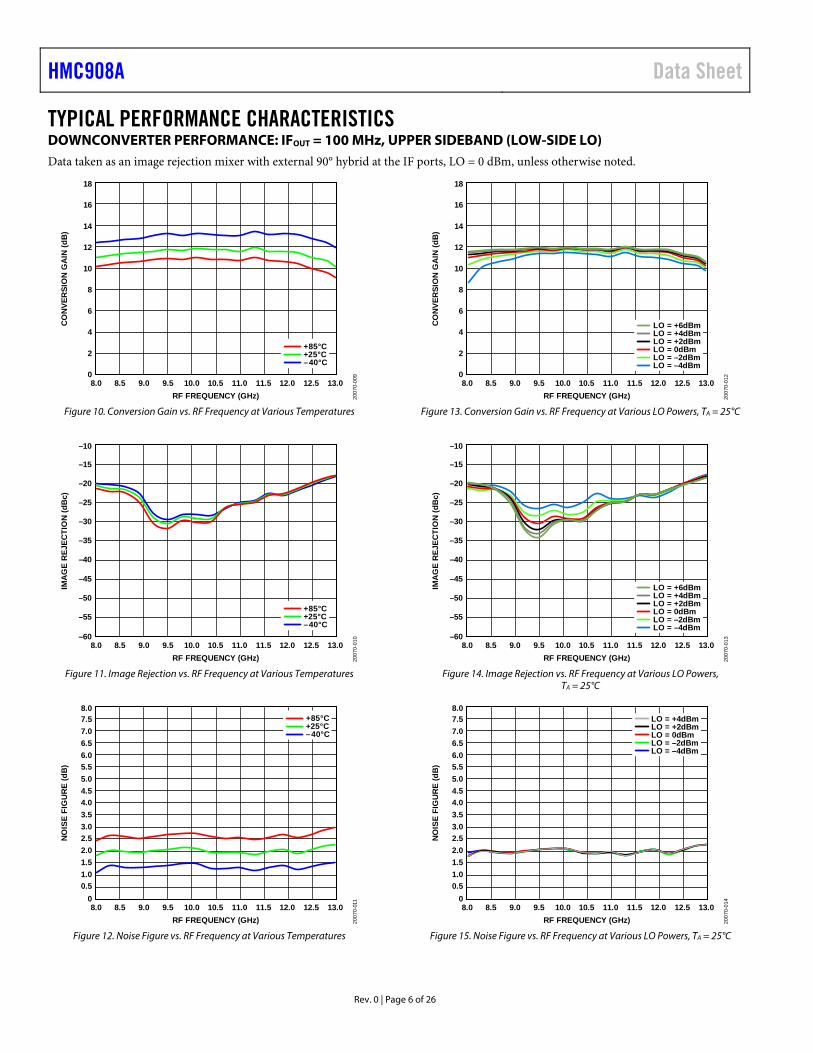
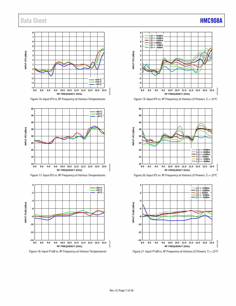
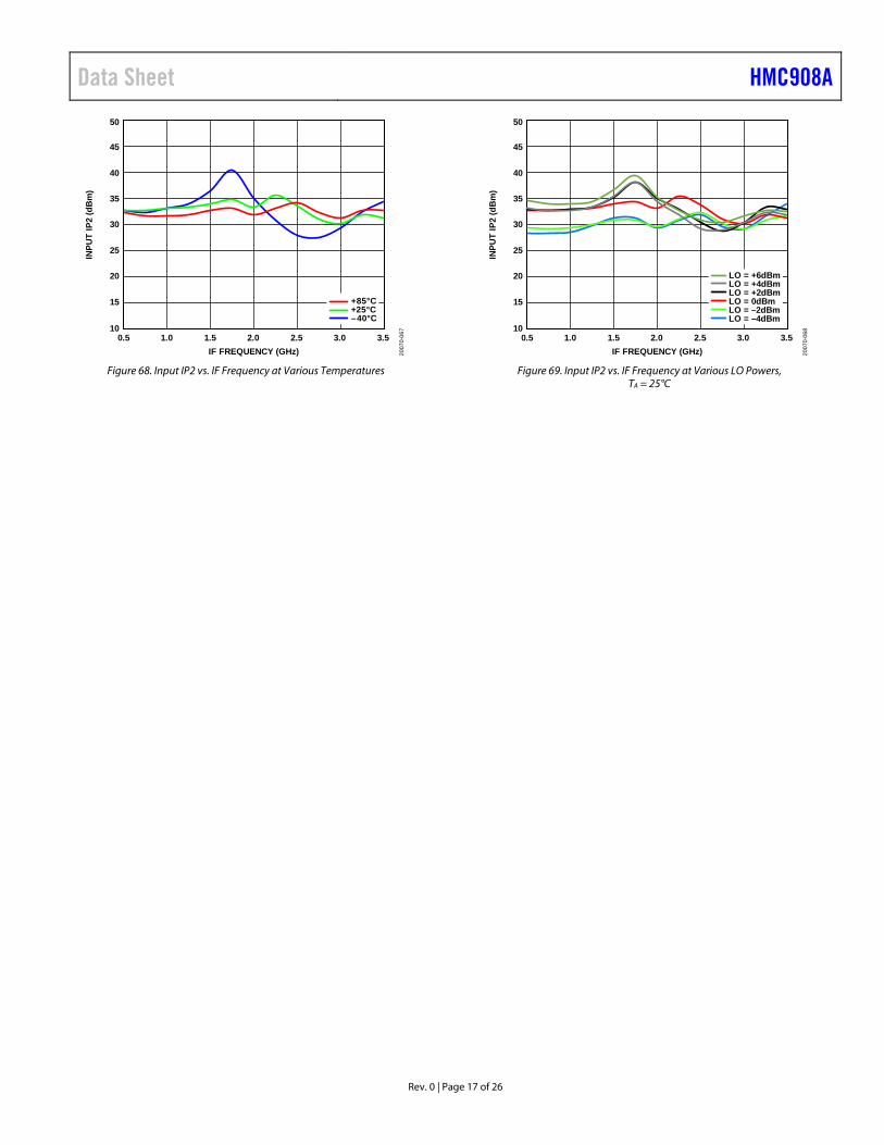
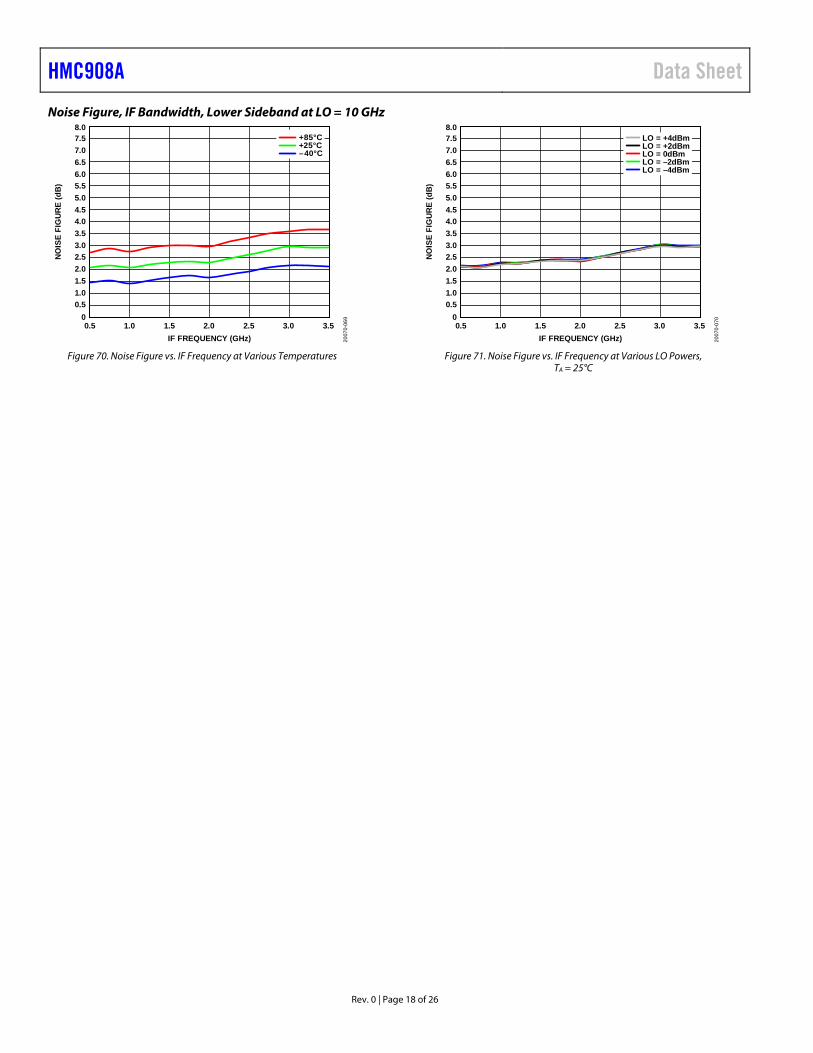
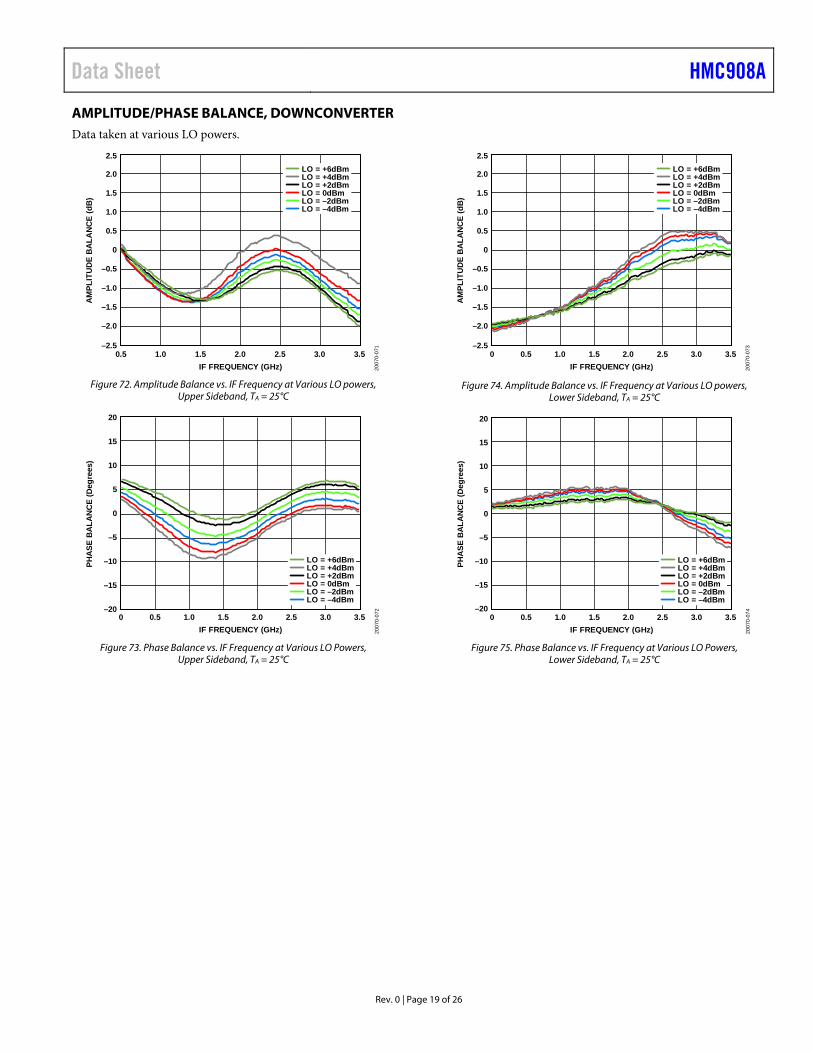
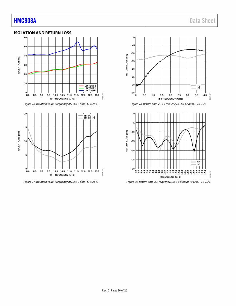
TYPICAL PERFORMANCE CHARACTERISTICS DOWNCONVERTER PERFORMANCE: IFOUT = 100 MHz, UPPER SIDEBAND (LOW-SIDE LO) Data taken as an image rejection mixer with external 90° hybrid at the IF ports, LO = 0 dBm, unless otherwise noted.
+85°C+25°C–40°C
8.0 13.0RF FREQUENCY (GHz)
8.5 9.0 9.5 10.0 10.5 11.0 11.5 12.0 12.5
18
0
4
10
14
16
8
2
6
12
CO
NVE
RSI
ON
GA
IN (d
B)
2007
0-00
9
Figure 10. Conversion Gain vs. RF Frequency at Various Temperatures
–10
–60
IMA
GE
REJ
ECTI
ON
(dB
c)
–55
–50
–45
–40
–35
–30
–25
–20
–15
+85°C+25°C–40°C
8.0 13.0RF FREQUENCY (GHz)
8.5 9.0 9.5 10.0 10.5 11.0 11.5 12.0 12.5
2007
0-01
0
Figure 11. Image Rejection vs. RF Frequency at Various Temperatures
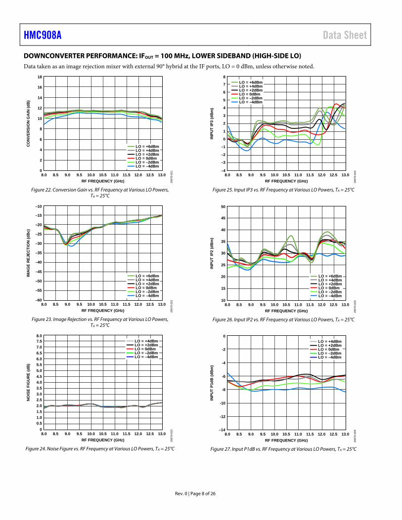
DOWNCONVERTER PERFORMANCE: IFOUT = 100 MHz, LOWER SIDEBAND (HIGH-SIDE LO) Data taken as an image rejection mixer with external 90° hybrid at the IF ports, LO = 0 dBm, unless otherwise noted.
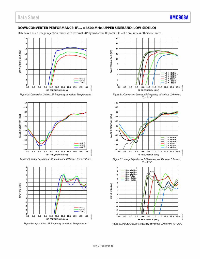
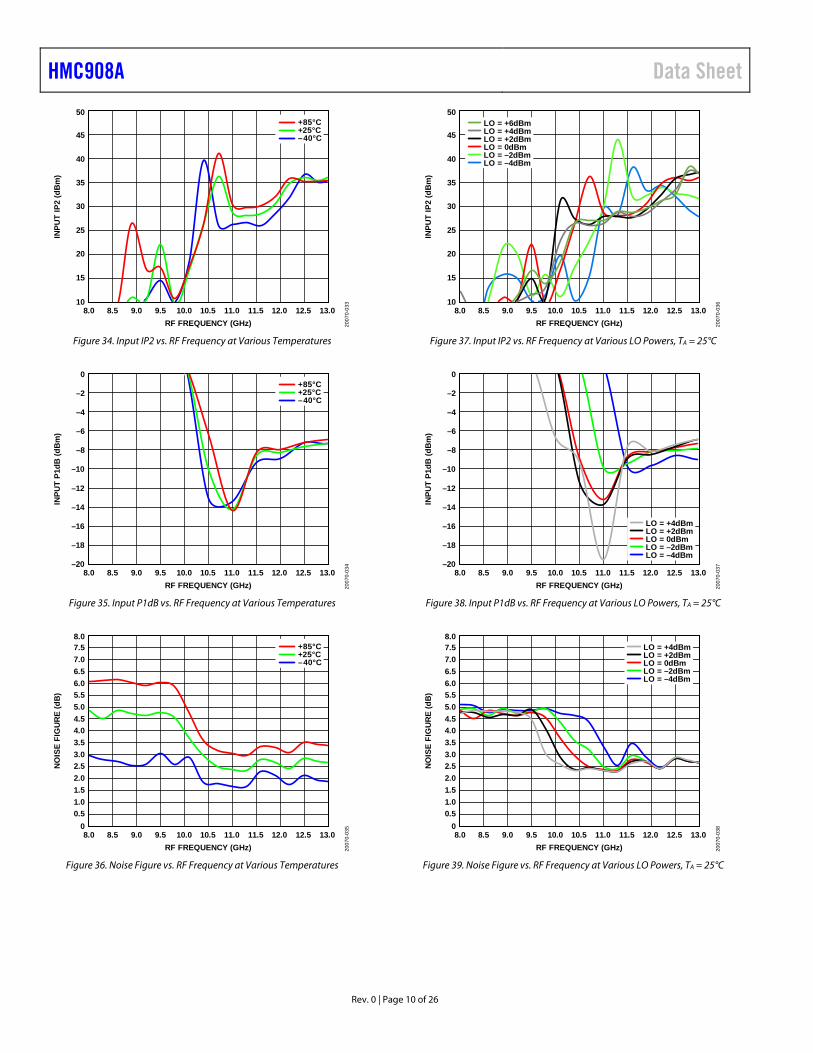
DOWNCONVERTER PERFORMANCE: IFOUT = 3500 MHz, UPPER SIDEBAND (LOW-SIDE LO) Data taken as an image rejection mixer with external 90° hybrid at the IF ports, LO = 0 dBm, unless otherwise noted.
8.0 13.0RF FREQUENCY (GHz)
8.5 9.0 9.5 10.0 10.5 11.0 11.5 12.0 12.5
18
0
4
10
14
16
8
2
6
12
CO
NVE
RSI
ON
GA
IN (d
B)
+85°C+25°C–40°C
2007
0-02
7
Figure 28. Conversion Gain vs. RF Frequency at Various Temperatures
–10
–60
IMA
GE
REJ
ECTI
ON
(dB
c)
–55
–50
–45
–40
–35
–30
–25
–20
–15
8.0 13.0RF FREQUENCY (GHz)
8.5 9.0 9.5 10.0 10.5 11.0 11.5 12.0 12.5
+85°C+25°C–40°C
2007
0-02
8
Figure 29. Image Rejection vs. RF Frequency at Various Temperatures
8
–4
INPU
T IP
3 (d
Bm
)
–3
–2
–1
0
1
2
3
4
5
6
7
8.0 13.0RF FREQUENCY (GHz)
8.5 9.0 9.5 10.0 10.5 11.0 11.5 12.0 12.5
+85°C+25°C–40°C
2007
0-02
9
Figure 30. Input IP3 vs. RF Frequency at Various Temperatures
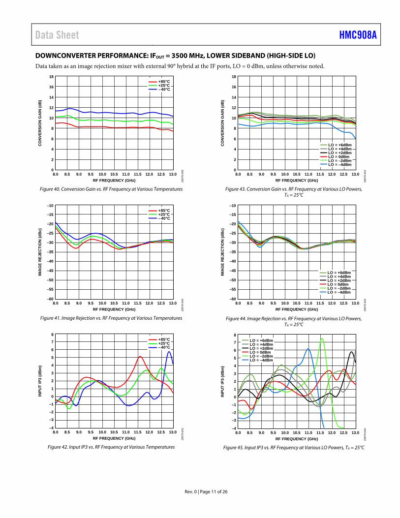
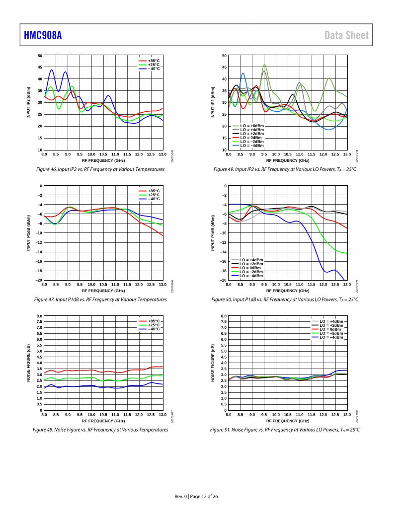
DOWNCONVERTER PERFORMANCE: IFOUT = 3500 MHz, LOWER SIDEBAND (HIGH-SIDE LO) Data taken as an image rejection mixer with external 90° hybrid at the IF ports, LO = 0 dBm, unless otherwise noted.
8.0 13.0RF FREQUENCY (GHz)
8.5 9.0 9.5 10.0 10.5 11.0 11.5 12.0 12.5
18
0
4
10
14
16
8
2
6
12
CO
NVE
RSI
ON
GA
IN (d
B)
+85°C+25°C–40°C
2007
0-03
9
Figure 40. Conversion Gain vs. RF Frequency at Various Temperatures
–10
–60
IMA
GE
REJ
ECTI
ON
(dB
c)
–55
–50
–45
–40
–35
–30
–25
–20
–15
8.0 13.0RF FREQUENCY (GHz)
8.5 9.0 9.5 10.0 10.5 11.0 11.5 12.0 12.5
+85°C+25°C–40°C
2007
0-04
0
Figure 41. Image Rejection vs. RF Frequency at Various Temperatures
8
–4
INPU
T IP
3 (d
Bm
)
–3
–2
–1
0
1
2
3
4
5
6
7
8.0 13.0RF FREQUENCY (GHz)
8.5 9.0 9.5 10.0 10.5 11.0 11.5 12.0 12.5
+85°C+25°C–40°C
2007
0-04
1
Figure 42. Input IP3 vs. RF Frequency at Various Temperatures
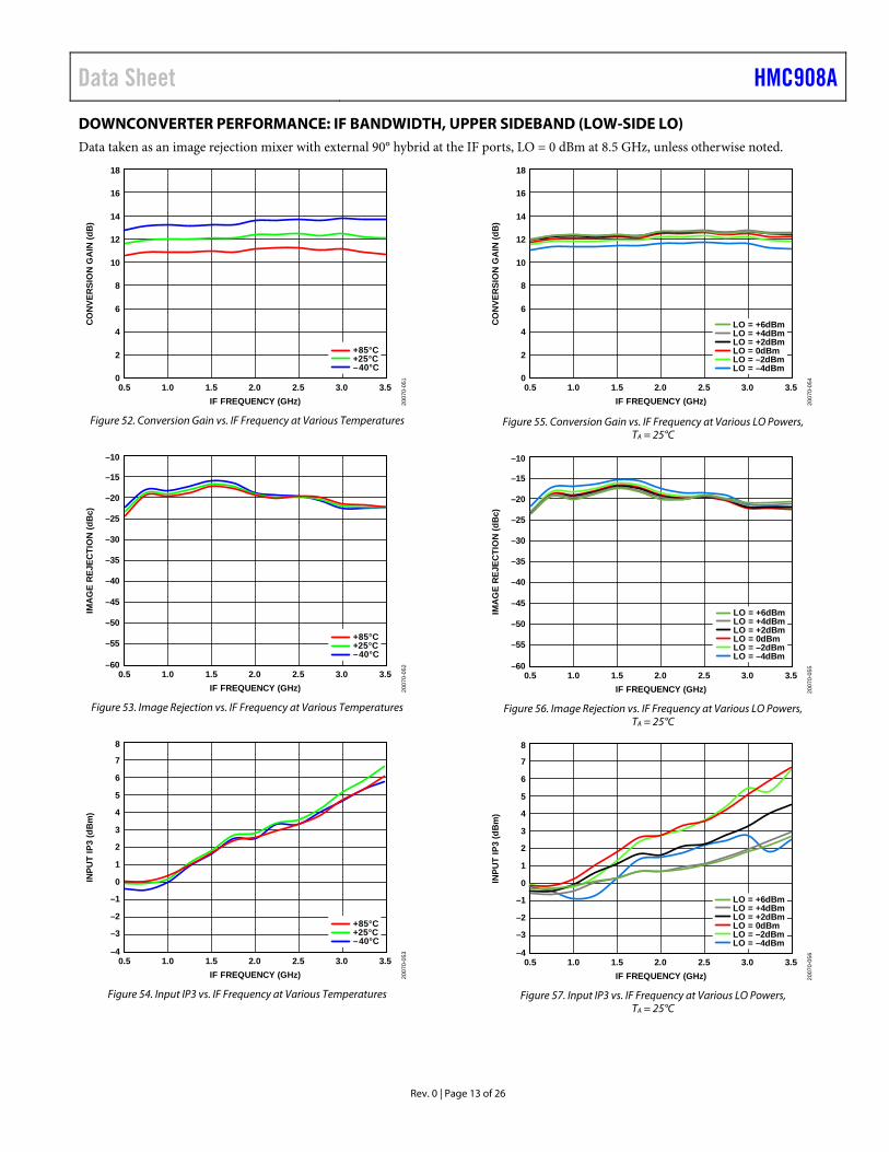
DOWNCONVERTER PERFORMANCE: IF BANDWIDTH, UPPER SIDEBAND (LOW-SIDE LO) Data taken as an image rejection mixer with external 90° hybrid at the IF ports, LO = 0 dBm at 8.5 GHz, unless otherwise noted.
0.5 3.5IF FREQUENCY (GHz)
1.0 1.5 2.0 2.5 3.0
18
0
4
10
14
16
8
2
6
12
CO
NVE
RSI
ON
GA
IN (d
B)
+85°C+25°C–40°C
2007
0-05
1
Figure 52. Conversion Gain vs. IF Frequency at Various Temperatures
–10
–60
IMA
GE
REJ
ECTI
ON
(dB
c)
–55
–50
–45
–40
–35
–30
–25
–20
–15
0.5 3.5IF FREQUENCY (GHz)
1.0 1.5 2.0 2.5 3.0
+85°C+25°C–40°C
2007
0-05
2
Figure 53. Image Rejection vs. IF Frequency at Various Temperatures
8
–4
INPU
T IP
3 (d
Bm
)
–3
–2
–1
0
1
2
3
4
5
6
7
0.5 3.5IF FREQUENCY (GHz)
1.0 1.5 2.0 2.5 3.0
+85°C+25°C–40°C
2007
0-05
3
Figure 54. Input IP3 vs. IF Frequency at Various Temperatures
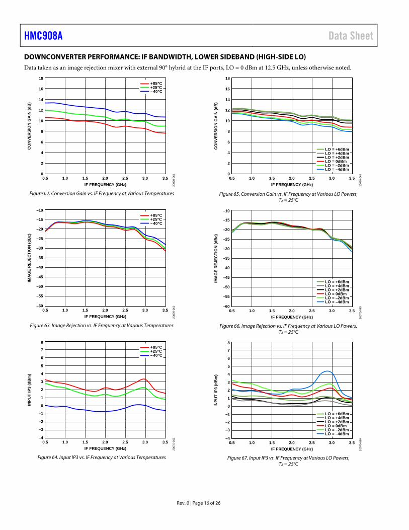
DOWNCONVERTER PERFORMANCE: IF BANDWIDTH, LOWER SIDEBAND (HIGH-SIDE LO) Data taken as an image rejection mixer with external 90° hybrid at the IF ports, LO = 0 dBm at 12.5 GHz, unless otherwise noted.
0.5 3.5IF FREQUENCY (GHz)
1.0 1.5 2.0 2.5 3.0
18
0
4
10
14
16
8
2
6
12
CO
NVE
RSI
ON
GA
IN (d
B)
+85°C+25°C–40°C
2007
0-06
1
Figure 62. Conversion Gain vs. IF Frequency at Various Temperatures
–10
–60
IMA
GE
REJ
ECTI
ON
(dB
c)
–55
–50
–45
–40
–35
–30
–25
–20
–15
0.5 3.5IF FREQUENCY (GHz)
1.0 1.5 2.0 2.5 3.0
+85°C+25°C–40°C
2007
0-06
2
Figure 63. Image Rejection vs. IF Frequency at Various Temperatures
8
–4
INPU
T IP
3 (d
Bm
)
–3
–2
–1
0
1
2
3
4
5
6
7
0.5 3.5IF FREQUENCY (GHz)
1.0 1.5 2.0 2.5 3.0
+85°C+25°C–40°C
2007
0-06
3
Figure 64. Input IP3 vs. IF Frequency at Various Temperatures
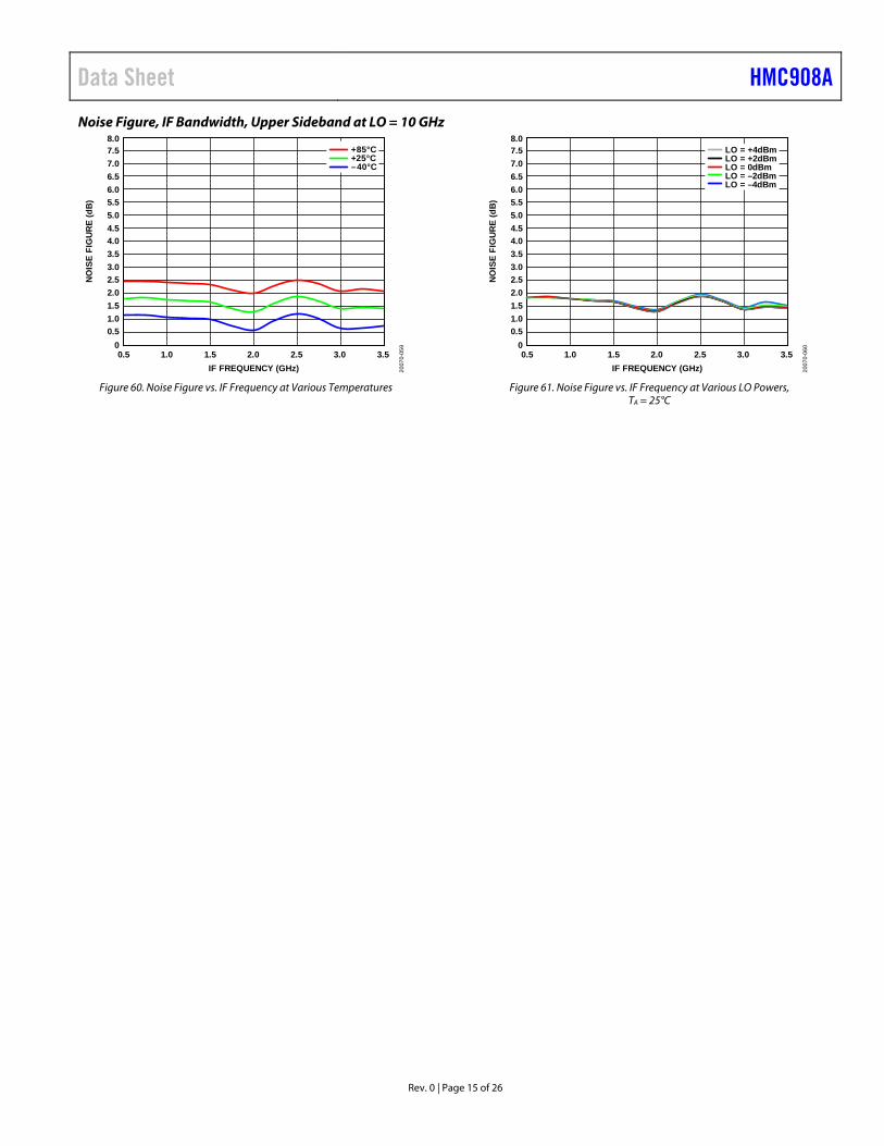
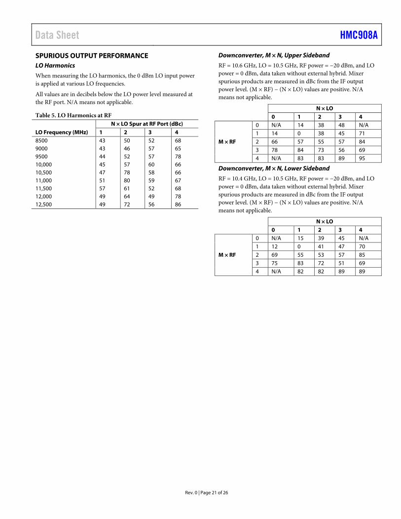
When measuring the LO harmonics, the 0 dBm LO input power is applied at various LO frequencies.
All values are in decibels below the LO power level measured at the RF port. N/A means not applicable.
Table 5. LO Harmonics at RF N × LO Spur at RF Port (dBc) LO Frequency (MHz) 1 2 3 4 8500 43 50 52 68 9000 43 46 57 65 9500 44 52 57 78 10,000 45 57 60 66 10,500 47 78 58 66 11,000 51 80 59 67 11,500 57 61 52 68 12,000 49 64 49 78 12,500 49 72 56 86
Downconverter, M × N, Upper Sideband
RF = 10.6 GHz, LO = 10.5 GHz, RF power = −20 dBm, and LO power = 0 dBm, data taken without external hybrid. Mixer spurious products are measured in dBc from the IF output power level. (M × RF) − (N × LO) values are positive. N/A means not applicable.
RF = 10.4 GHz, LO = 10.5 GHz, RF power = −20 dBm, and LO power = 0 dBm, data taken without external hybrid. Mixer spurious products are measured in dBc from the IF output power level. (M × RF) − (N × LO) values are positive. N/A means not applicable.
THEORY OF OPERATION The HMC908A is a compact, GaAs, MMIC, I/Q downconverter in a RoHS compliant package optimized for point to point and point to multipoint microwave radio applications operating in the 9 GHz to 12 GHz input RF frequency range. The HMC908A supports LO input frequencies of 8.5 GHz to 15.5 GHz and IF output frequencies of dc to 3.5 GHz.
The HMC908A uses an RF LNA amplifier followed by an I/Q double balanced mixer, where a driver amplifier drives the LO (see Figure 1).
LO DRIVER AMPLIFIER The LO driver amplifier takes a single LO input and amplifies it to the desired LO signal level for the mixer to operate optimally. The LO driver amplifier is self biased, and it only requires a single dc bias voltage (VD3) to operate. The bias current for the LO amplifier is 100 mA at 5 V, typically. The LO drive level of −4 dBm to +6 dBm makes it compatible with the Analog Devices, Inc., wideband synthesizer portfolio without the need for an external LO driver amplifier.
MIXER The mixer is an I/Q double balanced mixer, and this mixer topology reduces the need for filtering the unwanted sideband. An external 90° hybrid is required to select the desired sideband of operation.
LNA The LNA (RF amplifier) is self biased. The bias current for the LNA is 53 mA at 3 V, typically.
The typical application circuit (see Figure 81) shows the necessary external components on the bias lines to eliminate any undesired stability problems for the RF amplifier and the LO amplifier.
The HMC908A is a much smaller alternative to hybrid style image rejection converter assemblies, and it eliminates the need for wire bonding by allowing the use of surface-mount manufacturing assemblies.
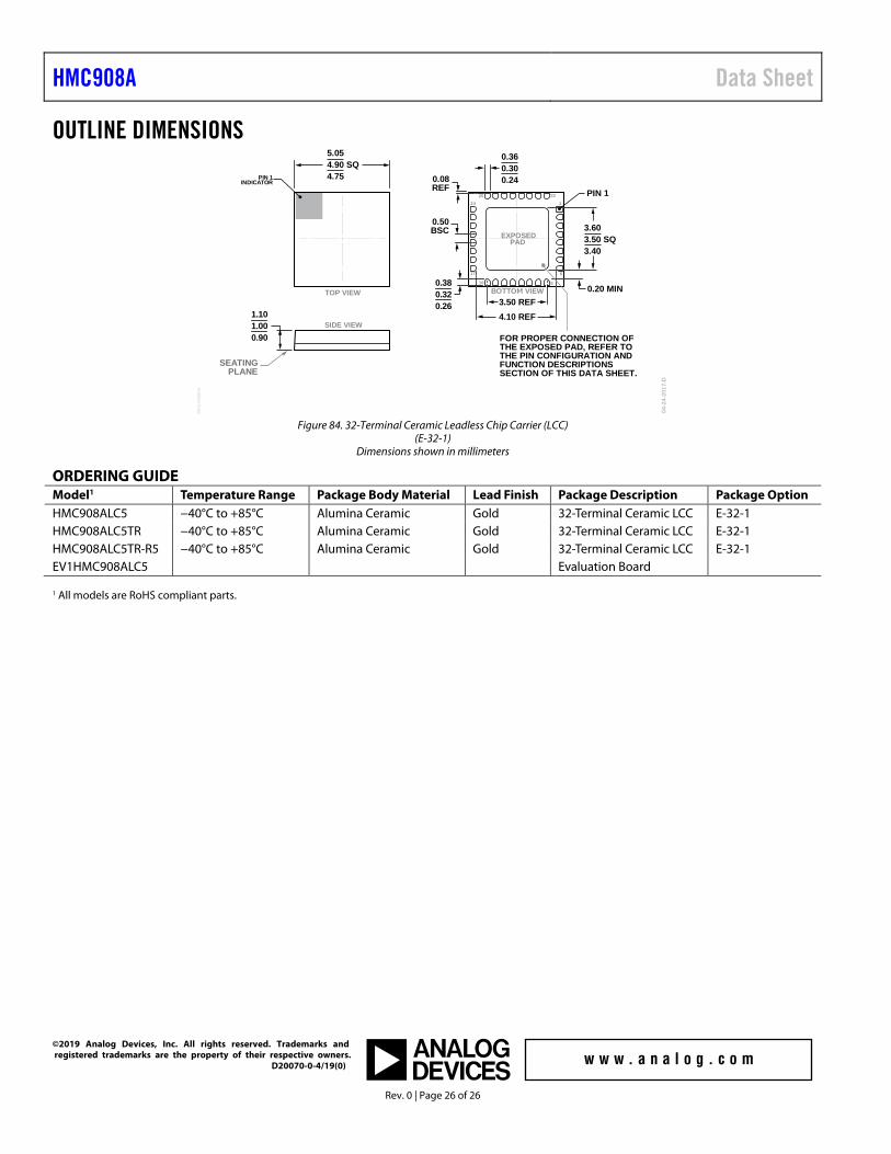
The HMC908A downconverter comes in a compact, 4.9 mm × 4.9 mm, 32-terminal ceramic LCC. The HMC908A operates over the −40°C to +85°C temperature range.
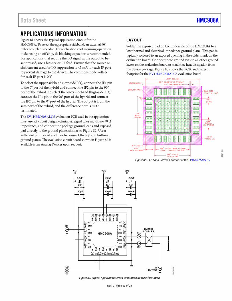
APPLICATIONS INFORMATION Figure 81 shows the typical application circuit for the HMC908A. To select the appropriate sideband, an external 90° hybrid coupler is needed. For applications not requiring operation to dc, using an off chip, dc blocking capacitor is recommended. For applications that require the LO signal at the output to be suppressed, use a bias tee or RF feed. Ensure that the source or sink current used for LO suppression is <5 mA for each IF port to prevent damage to the device. The common-mode voltage for each IF port is 0 V.
To select the upper sideband (low-side LO), connect the IF1 pin to the 0° port of the hybrid and connect the IF2 pin to the 90° port of the hybrid. To select the lower sideband (high-side LO), connect the IF1 pin to the 90° port of the hybrid and connect the IF2 pin to the 0° port of the hybrid. The output is from the sum port of the hybrid, and the difference port is 50 Ω terminated.
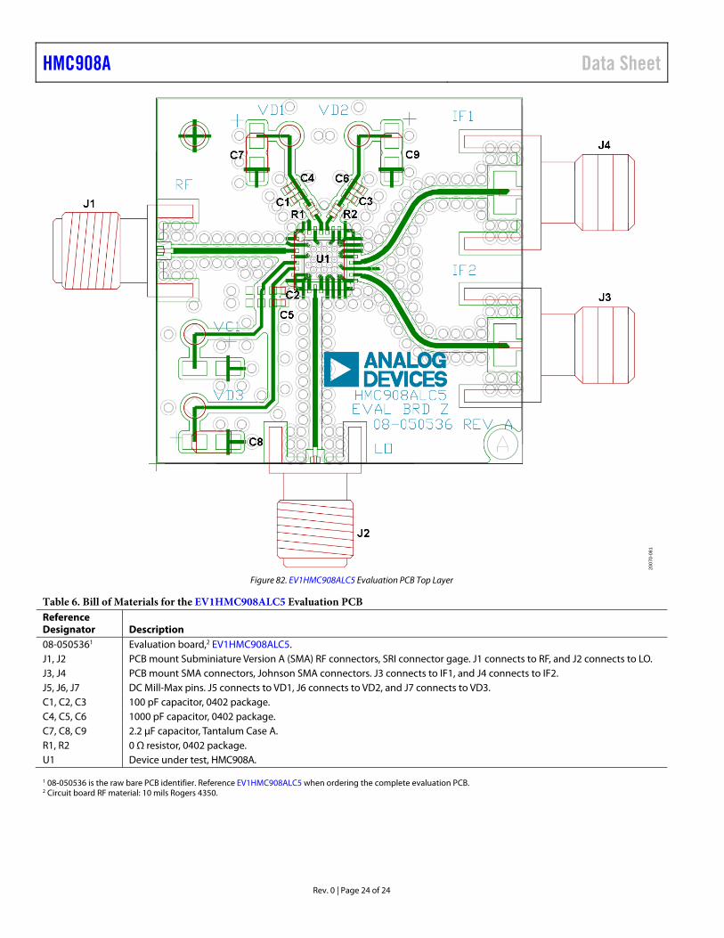
The EV1HMC908ALC5 evaluation PCB used in the application must use RF circuit design techniques. Signal lines must have 50 Ω impedance, and connect the package ground leads and exposed pad directly to the ground plane, similar to Figure 82. Use a sufficient number of via holes to connect the top and bottom ground planes. The evaluation circuit board shown in Figure 82 is available from Analog Devices upon request.
LAYOUT Solder the exposed pad on the underside of the HMC908A to a low thermal and electrical impedance ground plane. This pad is typically soldered to an exposed opening in the solder mask on the evaluation board. Connect these ground vias to all other ground layers on the evaluation board to maximize heat dissipation from the device package. Figure 80 shows the PCB land pattern footprint for the EV1HMC908ALC5 evaluation board.
2007
0-08
0
Figure 80. PCB Land Pattern Footprint of the EV1HMC908ALC5
+
2.2µF
VD3
1nF
100pF
NIC
NIC
NIC
VD1
VD2
NIC
NIC
NIC
NIC
GND
LO GND
NIC
NIC
NIC
NIC
NIC
GND
RF
GND
NIC
VD3
NIC
NIC
NIC
NIC
NIC
GND
IF1
GND
IF2
GND
+
2.2µF
VD1
1nF
100pF
+
2.2µF
VD2
1nF
100pF
RF
LO IFOUTPUT
IF2
IF1HYBRID
COUPLERHMC908A
9 10 11 12 13 14 15 16
32 31 30 29 28 27 26 25
24
23
22
21
20
19
18
17
1
2
3
4
5
6
7
8
2007
0-08
3
Figure 81. Typical Application Circuit Evaluation Board Information
Table 6. Bill of Materials for the EV1HMC908ALC5 Evaluation PCB Reference Designator Description 08-0505361 Evaluation board,2 EV1HMC908ALC5. J1, J2 PCB mount Subminiature Version A (SMA) RF connectors, SRI connector gage. J1 connects to RF, and J2 connects to LO. J3, J4 PCB mount SMA connectors, Johnson SMA connectors. J3 connects to IF1, and J4 connects to IF2. J5, J6, J7 DC Mill-Max pins. J5 connects to VD1, J6 connects to VD2, and J7 connects to VD3. C1, C2, C3 100 pF capacitor, 0402 package. C4, C5, C6 1000 pF capacitor, 0402 package. C7, C8, C9 2.2 μF capacitor, Tantalum Case A. R1, R2 0 Ω resistor, 0402 package. U1 Device under test, HMC908A. 1 08-050536 is the raw bare PCB identifier. Reference EV1HMC908ALC5 when ordering the complete evaluation PCB. 2 Circuit board RF material: 10 mils Rogers 4350.
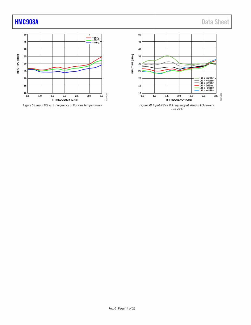
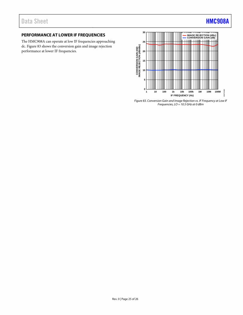
PERFORMANCE AT LOWER IF FREQUENCIES The HMC908A can operate at low IF frequencies approaching dc. Figure 83 shows the conversion gain and image rejection performance at lower IF frequencies.
30
25
20
15
10
5
01 10 100 1k 10k 100k 1M 10M 100M
CO
NVE
RSI
ON
GA
INA
ND
IMA
GE
REJ
ECTI
ON
(dB
/dB
c)
IF FREQUENCY (Hz)
IMAGE REJECTION (dBc)CONVERSION GAIN (dB)
2007
0-08
2
Figure 83. Conversion Gain and Image Rejection vs. IF Frequency at Low IF


![F3JR MB R20 1211[31731]ncandelier.free.fr/asus/ASUS_F3JR_R20.pdfH_D#50 H_TMS H_TDO H_TCK H_TRST# H_PREQ# +VCCP +VCCP +VCCP +VCCP GND GND GND GND GND GND GND TPC26T 1 T1 R8 1 2 56Ohm](https://static.documents.pub/doc/80x56/5faf0ab01979a324157ec2b6/f3jr-mb-r20-121131731-hd50-htms-htdo-htck-htrst-hpreq-vccp-vccp-vccp.jpg)


