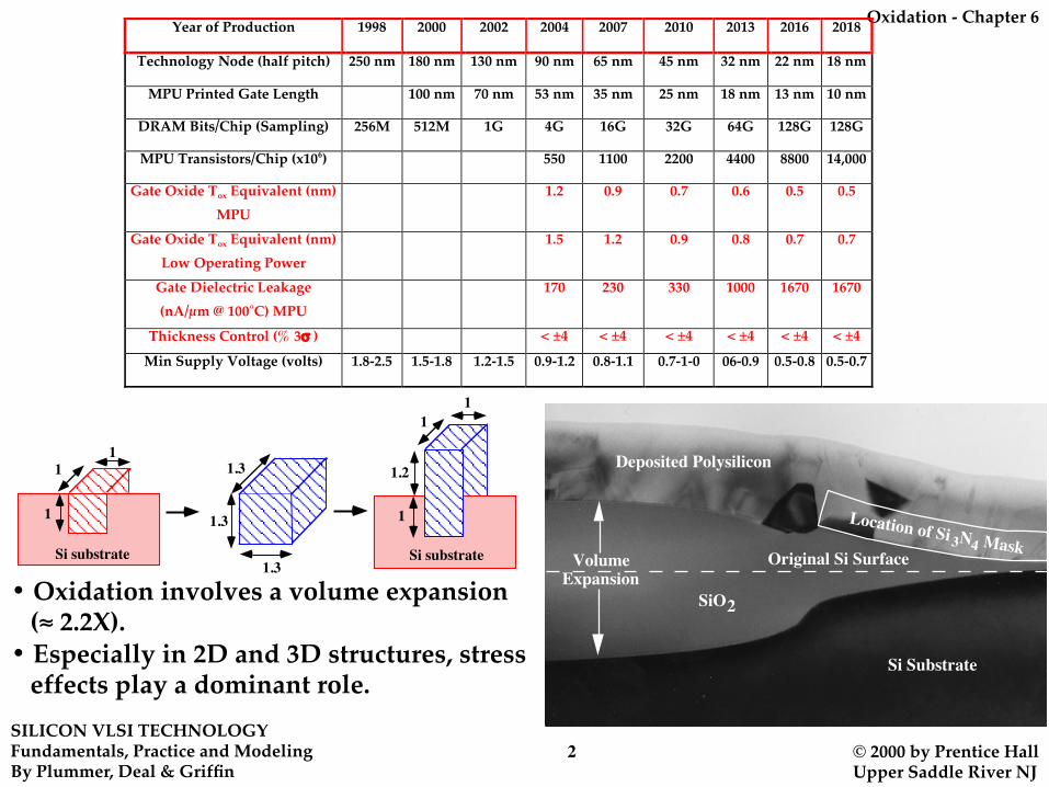
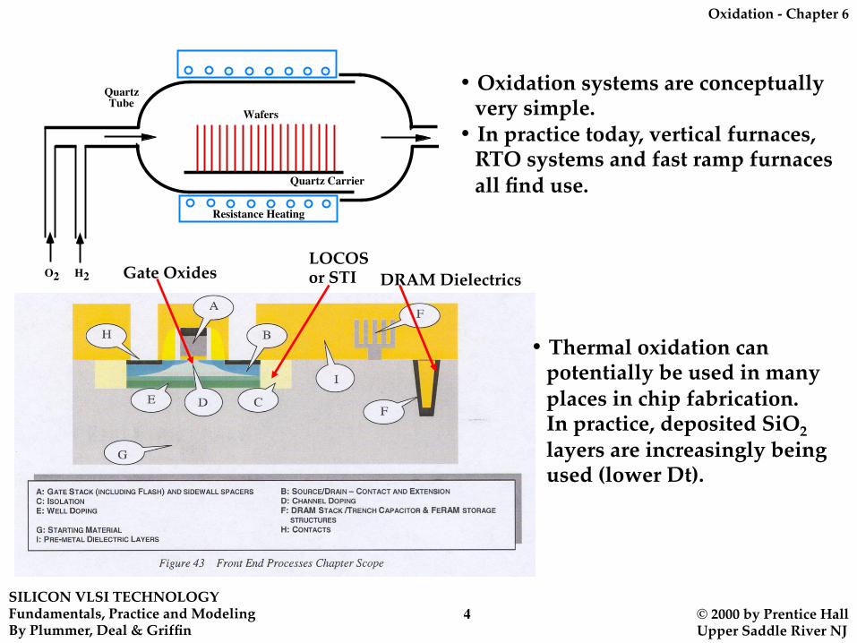
• Oxidation systems are conceptually very simple.• In practice today, vertical furnaces, RTO systems and fast ramp furnaces all find use.
• Thermal oxidation can potentially be used in many places in chip fabrication. In practice, deposited SiO2 layers are increasingly being used (lower Dt).
Gate OxidesLOCOSor STI DRAM Dielectrics
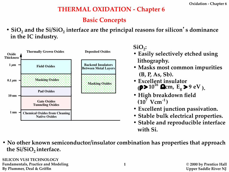
Oxidation - Chapter 6
SILICON VLSI TECHNOLOGYFundamentals, Practice and ModelingBy Plummer, Deal & Griffin
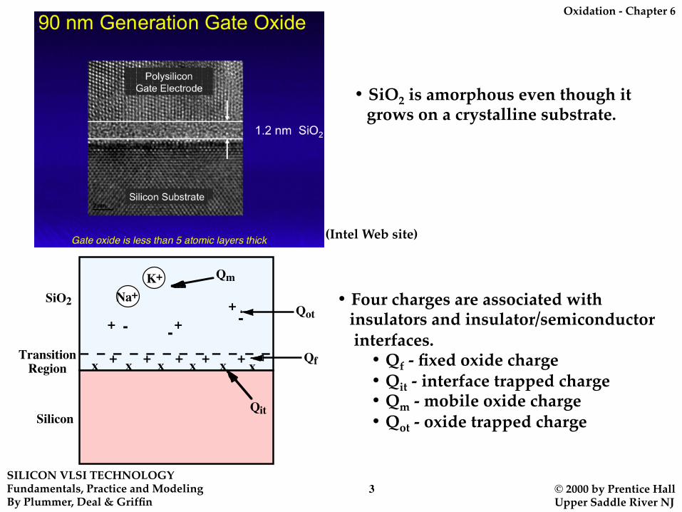
• Electric field lines pass through the “perfect” insulator and Si/SiO2 interface, into the substrate where they control charge carriers.• Accumulation, depletion and inversion result.• HF curve - inversion layer carriers cannot be generated fast enough to follow the AC signal so Cinv is Cox + CD.• LF curve - inversion layer carriers can be created and recombine at AC signal frequency so Cinv is just Cox.• Deep depletion - “DC” voltage is applied fast enough that inversion layer carriers cannot follow it, so CD must expand to balance the charge on the gate.• C-V measurements can be used to extract quantitative values for:
tox - oxide thickness NA - the substrate doping profile Qf, Qit, Qm, Qot - oxide, interface charges
Oxidation - Chapter 6
SILICON VLSI TECHNOLOGYFundamentals, Practice and ModelingBy Plummer, Deal & Griffin
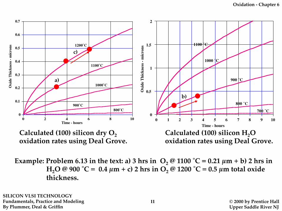
Calculated (100) silicon dry O2 oxidation rates using Deal Grove.
Calculated (100) silicon H2O oxidation rates using Deal Grove.
Example: Problem 6.13 in the text: a) 3 hrs in O2 @ 1100 ˚C = 0.21 µm + b) 2 hrs in H2O @ 900 ˚C = 0.4 µm + c) 2 hrs in O2 @ 1200 ˚C = 0.5 µm total oxide thickness.
a)
b)
c)
Oxidation - Chapter 6
SILICON VLSI TECHNOLOGYFundamentals, Practice and ModelingBy Plummer, Deal & Griffin
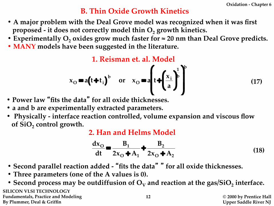
B. Thin Oxide Growth Kinetics• A major problem with the Deal Grove model was recognized when it was first proposed - it does not correctly model thin O2 growth kinetics.• Experimentally O2 oxides grow much faster for ≈ 20 nm than Deal Grove predicts.• MANY models have been suggested in the literature.
1. Reisman et. al. Model
�
xO = a t + t i( ) b or xO = a t + x i
a⎛ ⎝ ⎜
⎞ ⎠ ⎟
1b
⎛
⎝
⎜ ⎜ ⎜
⎞
⎠
⎟ ⎟ ⎟
b
(17)
• Power law “fits the data” for all oxide thicknesses.• a and b are experimentally extracted parameters.• Physically - interface reaction controlled, volume expansion and viscous flow of SiO2 control growth.
2. Han and Helms Model
�
dxO
dt= B1
2xO + A1+ B2
2xO + A2(18)
• Second parallel reaction added - “fits the data” ” for all oxide thicknesses.• Three parameters (one of the A values is 0).• Second process may be outdiffusion of OV and reaction at the gas/SiO2 interface.
Oxidation - Chapter 6
SILICON VLSI TECHNOLOGYFundamentals, Practice and ModelingBy Plummer, Deal & Griffin
• Second term added to Deal Grove model - higher dx/dt during initial growth.• L ≈ 7 nm, second term disappears for thicker oxides.• Easy to implement along with the DG model, \ used in process simulators.• Data agrees with the Reisman, Han and Massoud models. (800˚C dry O2 model comparison below.)
.
0
0.005
0.01
0.015
0.02
0.025
0.03
0 2 4 6 8 10
Oxi
de T
hick
ness
- m
icro
ns
Han & Helms Model
Reisman et. al. Model
Time - hours
Deal Grove Model (τ = 0)
Deal Grove Model (τ = 8 hrs)
Oxidation - Chapter 6
SILICON VLSI TECHNOLOGYFundamentals, Practice and ModelingBy Plummer, Deal & Griffin
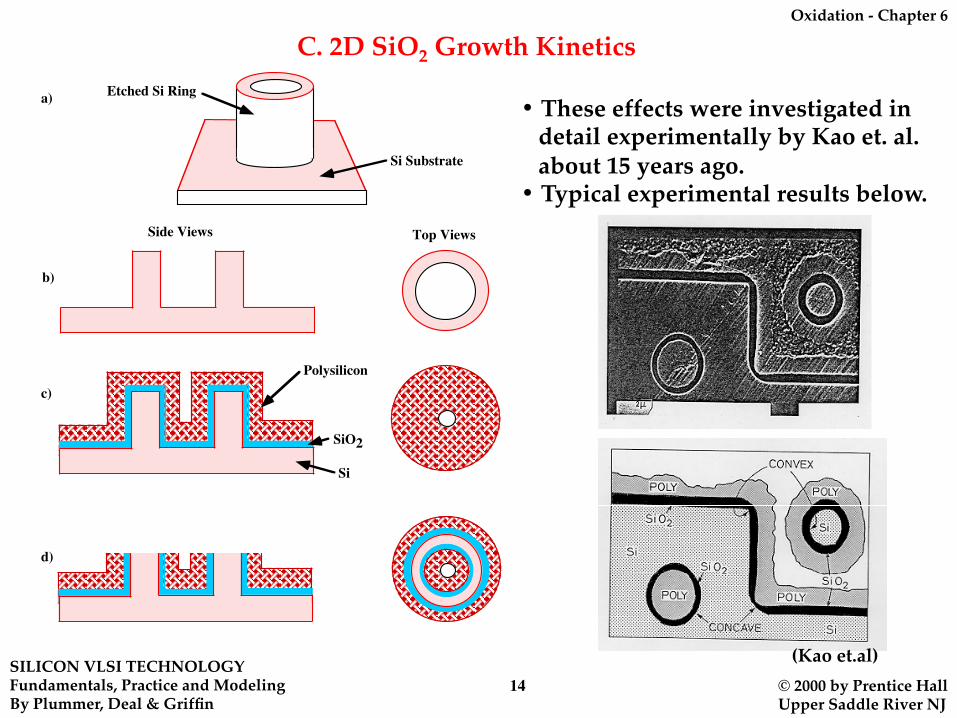
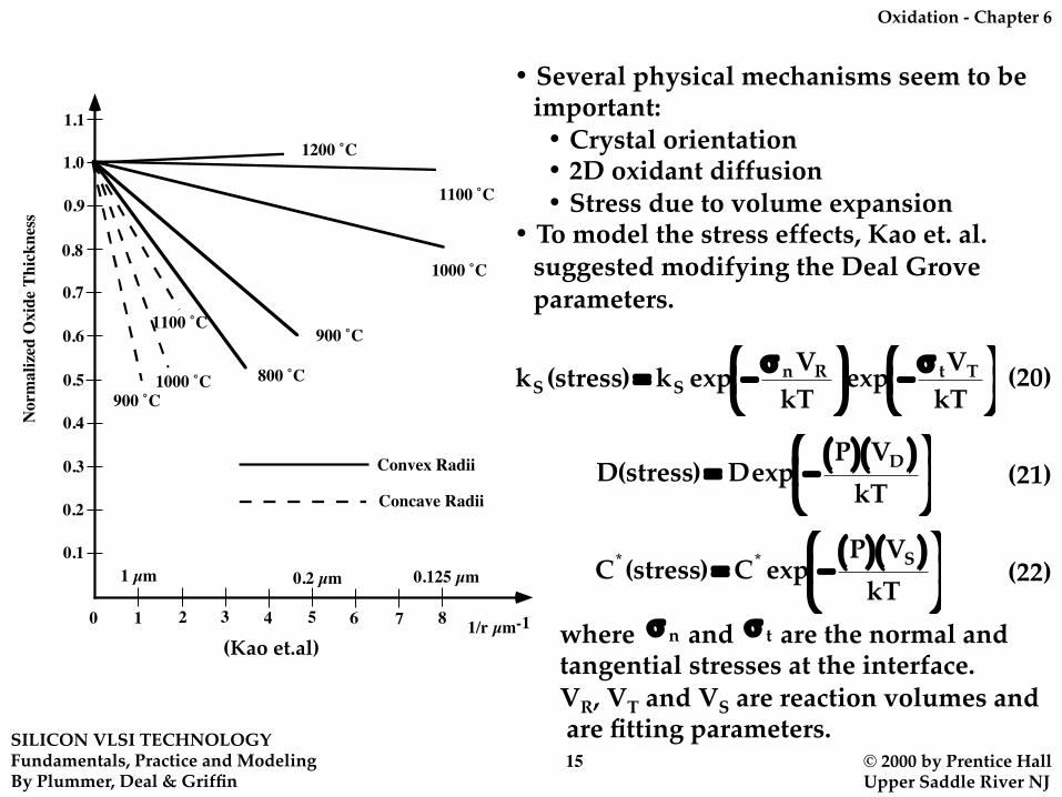
• Several physical mechanisms seem to be important: • Crystal orientation • 2D oxidant diffusion • Stress due to volume expansion• To model the stress effects, Kao et. al. suggested modifying the Deal Grove parameters.
�
kS (stress) = kS exp − σ nVR
kT⎛ ⎝ ⎜
⎞ ⎠ ⎟ exp − σ tVT
kT⎛ ⎝ ⎜
⎞ ⎠ ⎟
�
D(stress) = Dexp −P( ) VD( )
kT
⎛
⎝ ⎜
⎞
⎠ ⎟
�
C*(stress) = C* exp −P( ) VS( )
kT
⎛
⎝ ⎜
⎞
⎠ ⎟
(20)
(22)
(21)
where and are the normal and tangential stresses at the interface. VR, VT and VS are reaction volumes and are fitting parameters.
(Kao et.al)
�
σ n
�
σ t
Oxidation - Chapter 6
SILICON VLSI TECHNOLOGYFundamentals, Practice and ModelingBy Plummer, Deal & Griffin
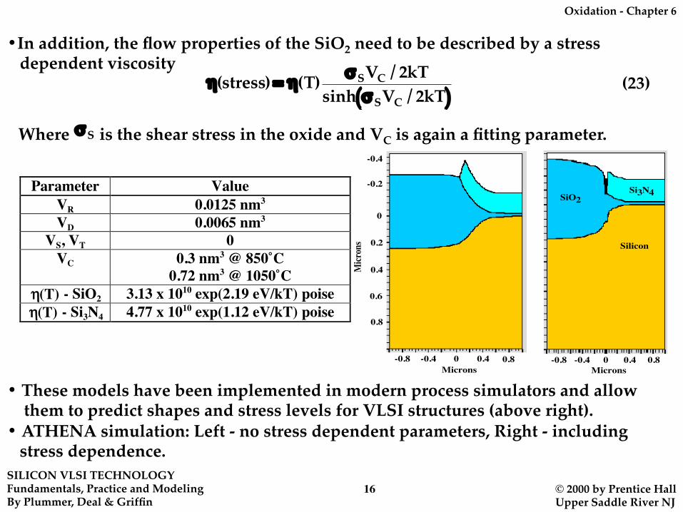
Where is the shear stress in the oxide and VC is again a fitting parameter.
�
σS
Parameter ValueVR 0.0125 nm3
VD 0.0065 nm3
VS, VT 0VC 0.3 nm3 @ 850˚C
0.72 nm3 @ 1050˚Cη(T) - SiO2 3.13 x 10¹⁰ exp(2.19 eV/kT) poiseη(T) - Si3N4 4.77 x 10¹⁰ exp(1.12 eV/kT) poise
• These models have been implemented in modern process simulators and allow them to predict shapes and stress levels for VLSI structures (above right).• ATHENA simulation: Left - no stress dependent parameters, Right - including stress dependence.
.
Silicon
SiO2Si3N4
0
0.2
0.4
0.6
0.8
-0.2
-0.4
MicronsMicrons
0 0.4 0.8-0.4-0.8Microns0 0.4 0.8-0.4-0.8
Oxidation - Chapter 6
SILICON VLSI TECHNOLOGYFundamentals, Practice and ModelingBy Plummer, Deal & Griffin
D. Point Defect Based Models• The oxidation models we have considered to this point are macroscopic models (diffusion coefficients, chemical reactions etc.).
*
*O2
H2O
Diffusion
Oxide Silicon
II
V
�
1 + 2γ( )SiSi + 2OI + 2βV↔ SiO2 + 2γI + stress
• There is also an atomistic picture of oxidation that has emerged in recent years.• Most of these ideas are driven by the volume expansion occurring during oxidation and the need for “free volume”.
• In Chapter 3 we described internal oxidation in the following way:
(24)
• Surface oxidation can be thought of in the same way.
Oxidation - Chapter 6
SILICON VLSI TECHNOLOGYFundamentals, Practice and ModelingBy Plummer, Deal & Griffin
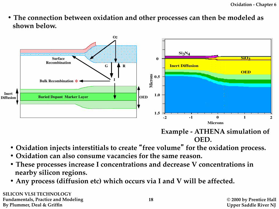
• The connection between oxidation and other processes can then be modeled as shown below.
Buried Dopant Marker Layer
G R
Bulk Recombination
SurfaceRecombination
*
OEDInert
Diffusion
O2
I
.
Inert DiffusionOED
Micr
ons
0
0.5
1.0
1.5
Microns0 1 2-1-2
Si3N4SiO2
Example - ATHENA simulation of OED.
• Oxidation injects interstitials to create “free volume” for the oxidation process.• Oxidation can also consume vacancies for the same reason.• These processes increase I concentrations and decrease V concentrations in nearby silicon regions.• Any process (diffusion etc) which occurs via I and V will be affected.
Oxidation - Chapter 6
SILICON VLSI TECHNOLOGYFundamentals, Practice and ModelingBy Plummer, Deal & Griffin
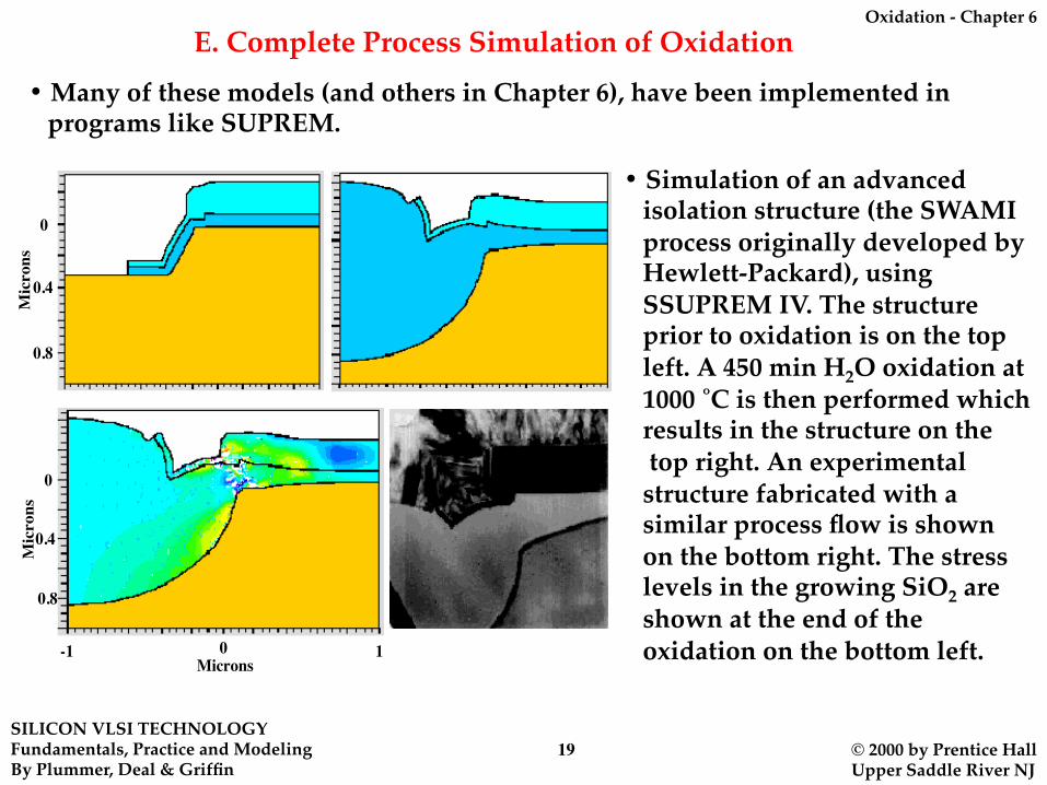
E. Complete Process Simulation of Oxidation• Many of these models (and others in Chapter 6), have been implemented in programs like SUPREM.
.
0
0.4
0.8
Microns
0
0.4
0.8
Microns
Microns1-1 0
• Simulation of an advanced isolation structure (the SWAMI process originally developed by Hewlett-Packard), using SSUPREM IV. The structure prior to oxidation is on the top left. A 450 min H2O oxidation at 1000 ˚C is then performed which results in the structure on the top right. An experimental structure fabricated with a similar process flow is shown on the bottom right. The stress levels in the growing SiO2 are shown at the end of the oxidation on the bottom left.
Oxidation - Chapter 6
SILICON VLSI TECHNOLOGYFundamentals, Practice and ModelingBy Plummer, Deal & Griffin