31
P-N junction
| Date post: | 21-Mar-2017 |
| Category: |
Science |
| Upload: | debi-prasad-dash |
| View: | 181 times |
| Download: | 1 times |
P-N junction

I
+ V –
Circuit symbol
P-N Junction
Donor ions
N-type
P-type
P-type semiconductor in contact withN-type semiconductor forms a P-Njunction
To a semiconductor, one side electronsand other side holes are injected
Or to a P-type semiconductor a layer ofelectrons are diffused or vice versa.
P-N junctions are the basic unit of allsemiconductor devices; at least onejunction
Used as rectifiers, switching devices,solar cells, laser diodes and LEDs
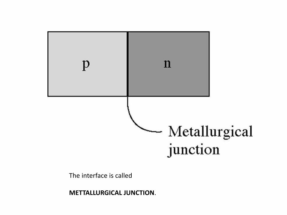
The interface is called
METTALLURGICAL JUNCTION.
n-typep-typeNdNa
pp0= Na nn0= Nd
a
2i
0pN
nn
d
2i
0nN
np
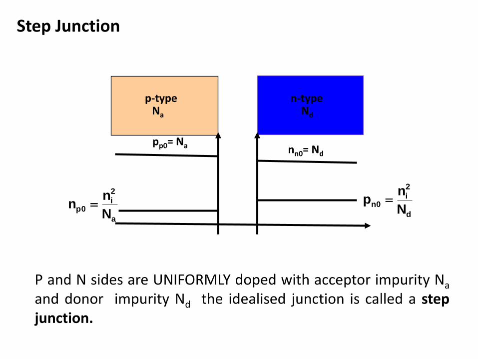
Step Junction
P and N sides are UNIFORMLY doped with acceptor impurity Na
and donor impurity Nd the idealised junction is called a stepjunction.
n=0p=0

BASIC STRUCTURE
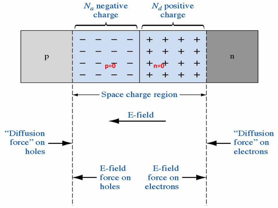
1.Due to density gradient of the majority carriers across the junction, carrier diffusion takes place.2. Recombination of majority carriers across the junction leaves behind positive
dopant ions on the N-side and negative dopant ions on the P-side.
3. Separation of charge creates a POTENTIAL DIFFERENCE at the junction and an ELECTRIC FIELD is established directed from N to P side of the junction.
4. In a region on both sides of the junction free carriers (electrons and holes) are absent, this is called DEPLETION LAYER or SPACE CHARGE REGION
5. Outside this region density gradient and diffusion force on the majority carriers exist.
6. At equilibrium, the diffusion force is balanced by the electric force on the carriers.

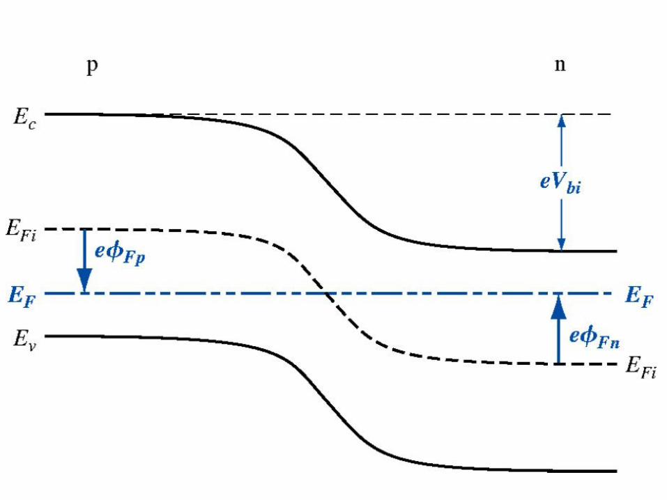
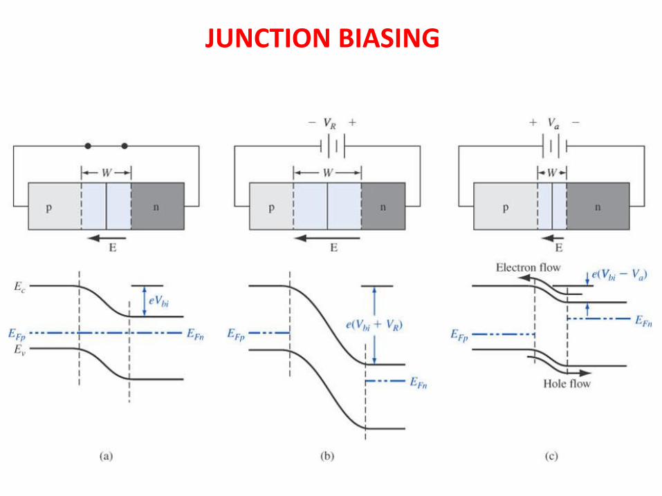
No voltage applied to the junction– P-N junction at thermal equilibrium
This is called ZERO BIASING.
Majority carriers from both side experience a POTENTIAL BARRIER due to the electric field at the junction.
This barrier at the junction is called BUILT-IN-POTENTIAL BARRIER.
BUILT-IN-POTENTIAL BARRIER ( Vbi) maintains equilibrium between the carriers across the junction and prevents further recombination across the junction.
Vbi is calculated as it can not be measured directly.
In the depletion layer, n=0 and p=0
FERMI LEVEL is constant throughout the system.
A bending of band observed from P to N side.

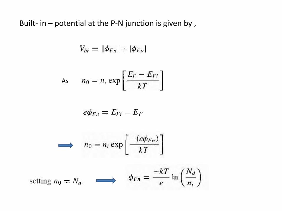
Built- in – potential at the P-N junction is given by ,
As

Nd and Na will denote the net donor andacceptor concentrations in the individualn and p regions, respectively
As lower Ec means a higher voltage, the N side is at a higher voltage or electrical potential than the P side.
Similarly,

ELECTRIC FIELD
POTENTIAL
Emax

REVERSE BIAS PN JUNCTION
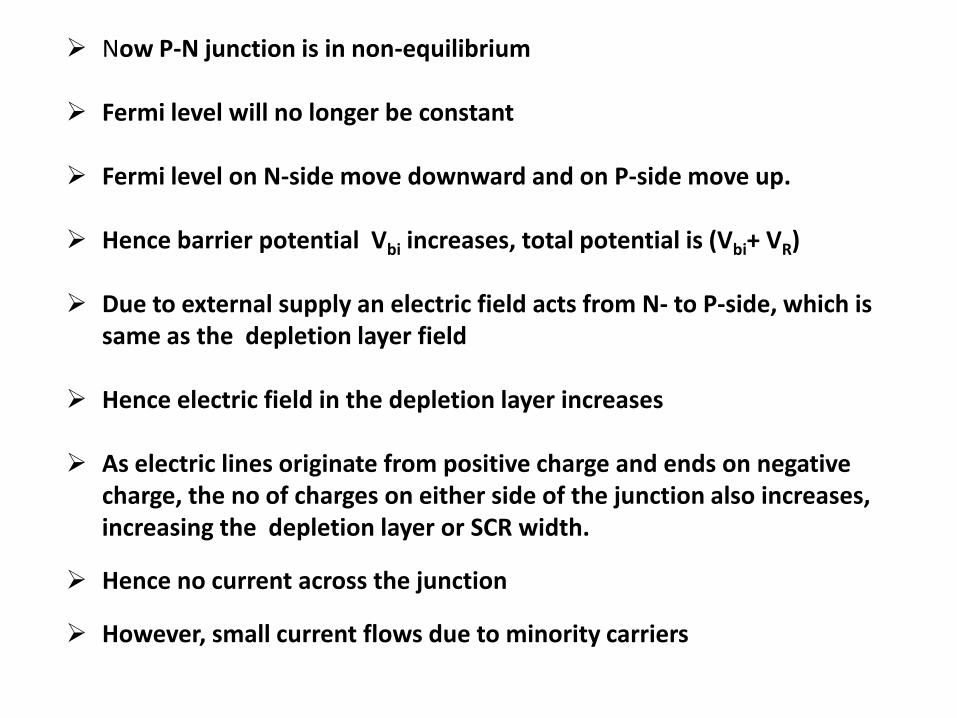
Now P-N junction is in non-equilibrium
Fermi level will no longer be constant
Fermi level on N-side move downward and on P-side move up.
Hence barrier potential Vbi increases, total potential is (Vbi+ VR)
Due to external supply an electric field acts from N- to P-side, which is same as the depletion layer field
Hence electric field in the depletion layer increases
As electric lines originate from positive charge and ends on negative charge, the no of charges on either side of the junction also increases,increasing the depletion layer or SCR width.
Hence no current across the junction
However, small current flows due to minority carriers
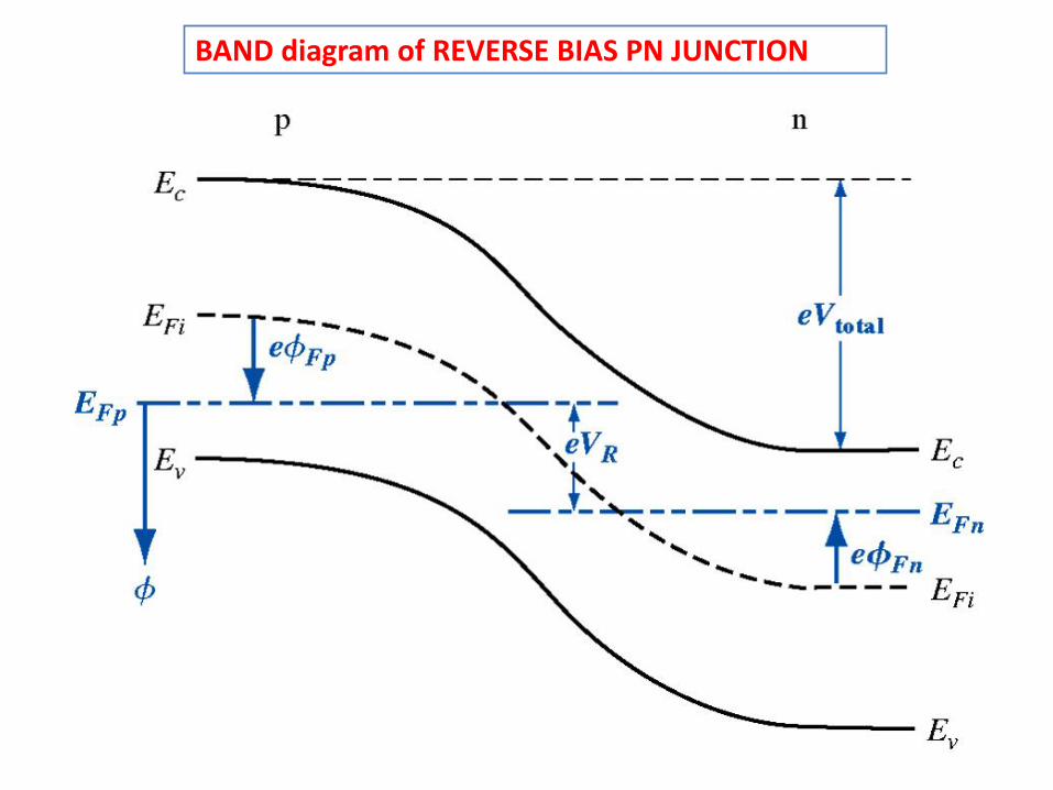
BAND diagram of REVERSE BIAS PN JUNCTION

Breakdown Mechanism:
Breakdown occurs by two mechanisms.
• Avalanche BreakdownEnergetic carriers ionize host atoms and there is carrier multiplication leading to breakdown.
• Zener BreakdownElectrons from p-region can tunnel to the conduction band in the n-region causing breakdown.
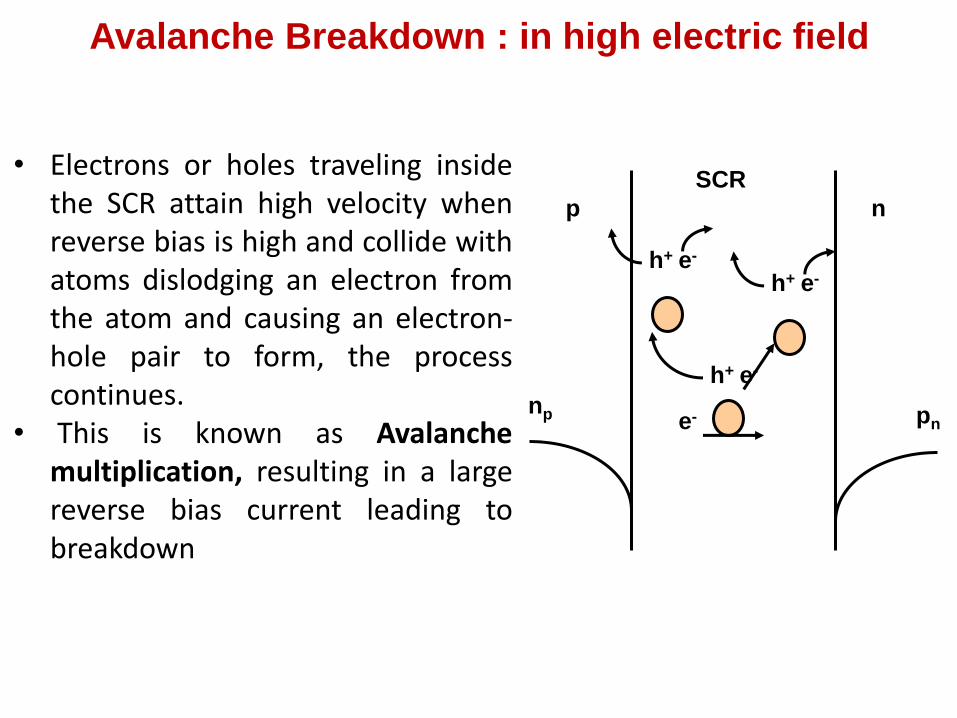
Avalanche Breakdown : in high electric field
• Electrons or holes traveling insidethe SCR attain high velocity whenreverse bias is high and collide withatoms dislodging an electron fromthe atom and causing an electron-hole pair to form, the processcontinues.
• This is known as Avalanchemultiplication, resulting in a largereverse bias current leading tobreakdown
np pn
p n
SCR
e-
e-h+
e-h+e-h+
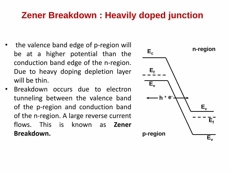
Zener Breakdown : Heavily doped junction
• the valence band edge of p-region willbe at a higher potential than theconduction band edge of the n-region.Due to heavy doping depletion layerwill be thin.
• Breakdown occurs due to electrontunneling between the valence bandof the p-region and conduction bandof the n-region. A large reverse currentflows. This is known as ZenerBreakdown.
Ec
Ev
Ef
Ec
Ef
Ev
p-region
n-region
e-h +
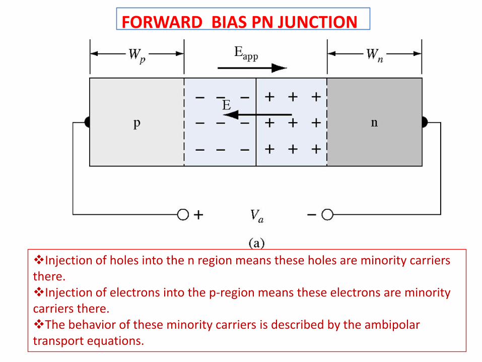
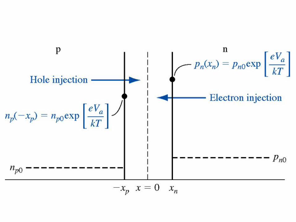
FORWARD BIAS PN JUNCTION
Injection of holes into the n region means these holes are minority carriers there.Injection of electrons into the p-region means these electrons are minority carriers there.The behavior of these minority carriers is described by the ambipolar transport equations.

Forward Biasing
The applied forward biasing potential Va reduces the depletion layerpotential to (Vbi-Va).
Since the applied field is in the opposite direction now the net EF isreduced , so thermal eqbm. is also disturbed.
The electric field force that prevented majority carriers from crossingthe space charge region is reduced.
Majority carrier electrons from the n side are now injected acrossthe depletion region into the p material, and majority carrier holesfrom the p side are injected across the depletion region .
As long as the bias Va is applied, the injection of carriers across thespace charge region continues and a current is created in the pnjunction
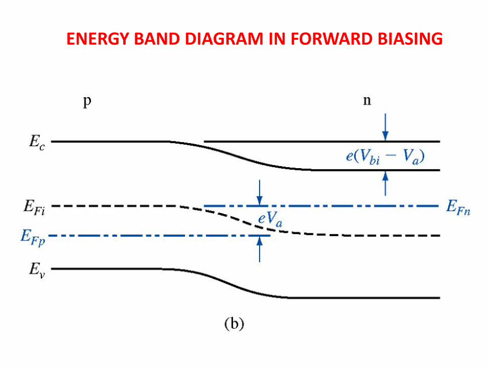
ENERGY BAND DIAGRAM IN FORWARD BIASING

Minority Carrier Distribution
For excess minority carrier holes in an n region
For excess minority carrier electrons in p region
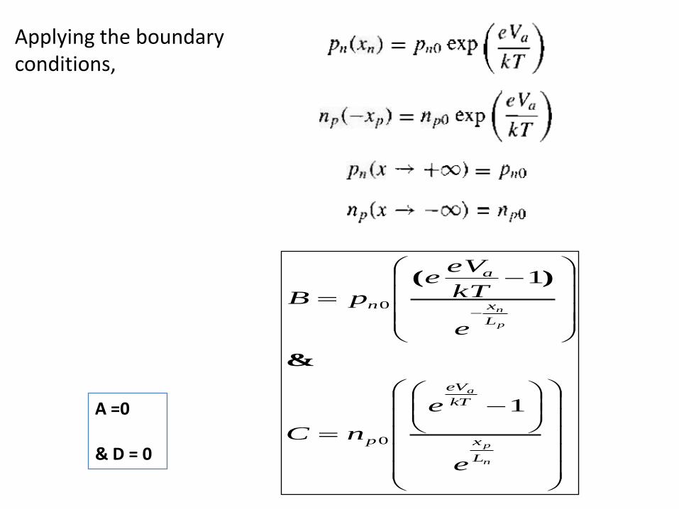
Applying the boundary conditions,
n
p
a
p
n
L
x
kT
eV
p
L
x
a
n
e
e
nC
e
kT
eVe
pB
1
1
0
0
&
)(
A =0
& D = 0

)(
)()(,
n
p
nkT
eV
n
nnn
xxL
xxeep
pxpxpso
a
10
0
)(
)()(&,
p
n
pkT
eV
p
ppp
xxL
xxeen
nxnxn
a
10
0
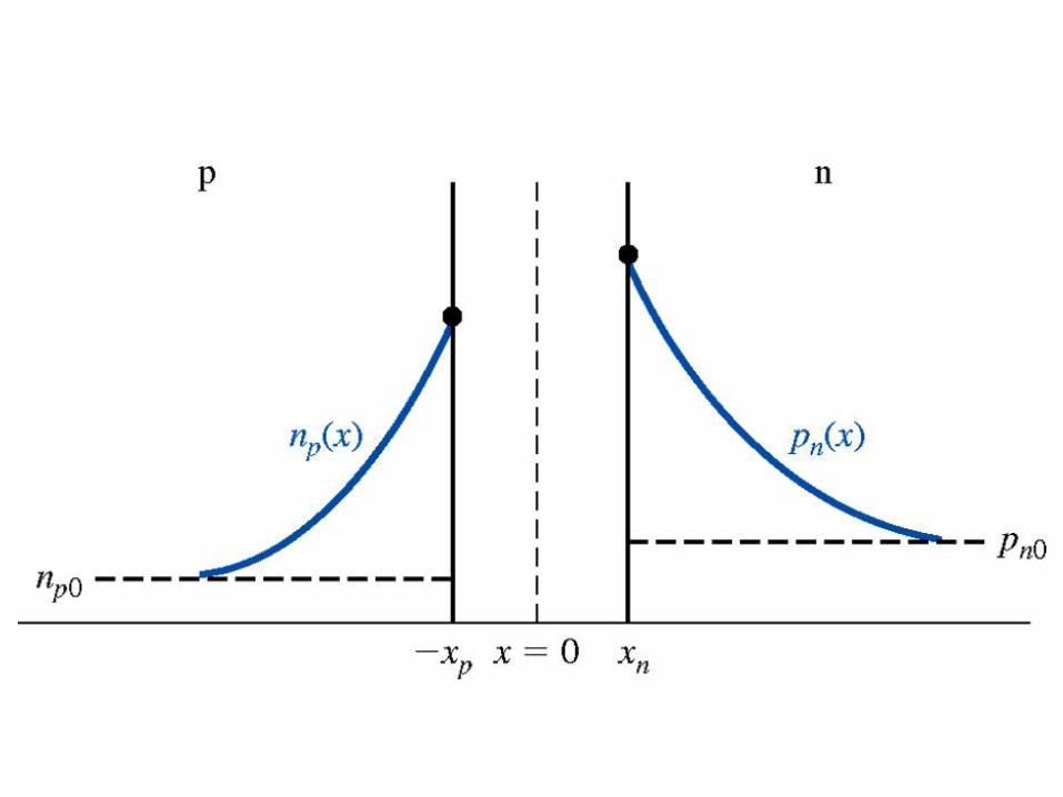
The minority carrier concentrations decay exponentially with distance away from the junction to their thermal-equilibrium values

IDEAL PN JUNCTION CURRENT
both electron and hole current density are in the +x direction.
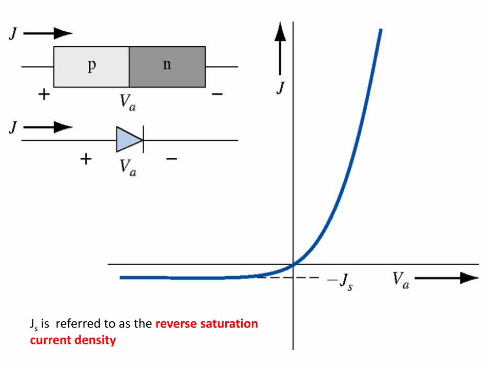
Js is referred to as the reverse saturation current density

Ideal reverse saturation current density Js , is a function of the thermal-equilibrium minority carrier concentrations np0 and pn0 , which are proportional to ni, which is a very strong function of temperature.
Forward-bias current-voltage relation has Js and
As temperature increases, less forward-bias voltage is required to obtain the same diode current. If the voltage is constant, the diode current will increase as temperature increases
Which makes the forward-bias current-voltage relation a function of temperature
Effect of temperature

The IV curves of the silicon PN diode shift to lower voltages with increasing temperature
JUNCTION BIASING


