30
P51: High Performance Networking Lecture 4: High Throughput Devices Dr Noa Zilberman [email protected] Lent 2018/19
P51: High Performance NetworkingLecture 4: High Throughput Devices
Dr Noa [email protected] Lent 2018/19
Very High Throughput Switches

12.8Tbps Switches!
Lets convert this to packet rate requirements:
5.8 Gpps @ 256B
19.2 Gpps @ 64B
But clock rate is only ~1GHz….
The Truth About Switch Silicon Design
02468
101214161820
50 250 450 650 850 1050 1250 1450
Req
uire
d Pa
ralle
lism
Packet Size [B]
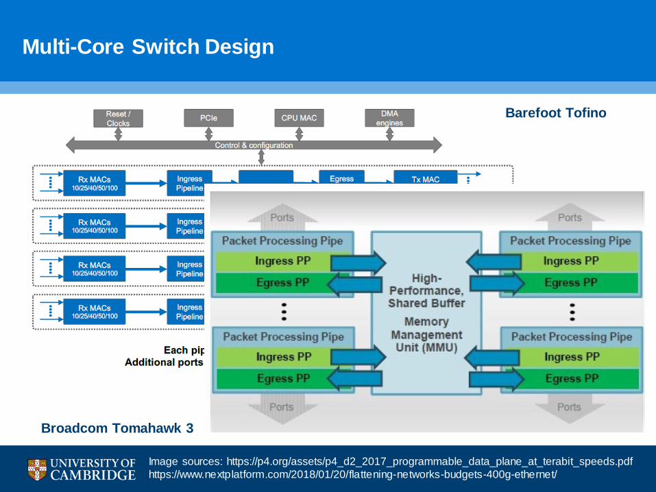
Multi-Core Switch Design
Broadcom Tomahawk 3
Barefoot Tofino
Image sources: https://p4.org/assets/p4_d2_2017_programmable_data_plane_at_terabit_speeds.pdfhttps://www.nextplatform.com/2018/01/20/flattening-networks-budgets-400g-ethernet/
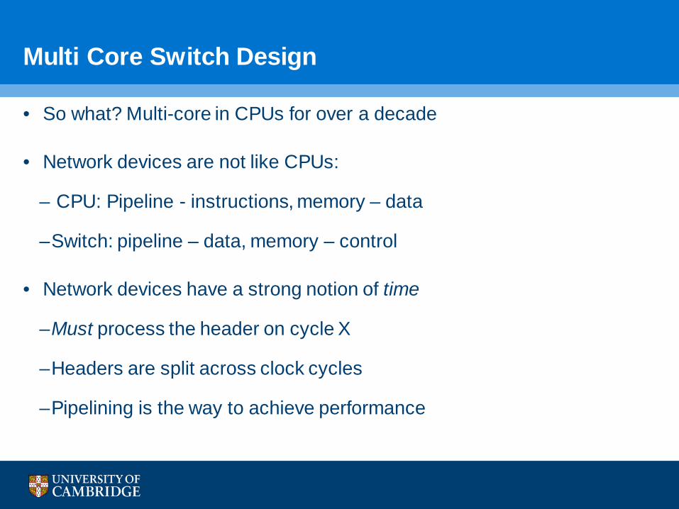
• So what? Multi-core in CPUs for over a decade
• Network devices are not like CPUs:
– CPU: Pipeline - instructions, memory – data
–Switch: pipeline – data, memory – control
• Network devices have a strong notion of time
–Must process the header on cycle X
–Headers are split across clock cycles
–Pipelining is the way to achieve performance
Multi Core Switch Design

• The limitations of processing packets in the host:
• DPDK is a popular set of libraries and drivers for fast packet processing
• DPDK can process a packet in 80 clock cycles
– Lets assume 4GHz clock (0.25ns/cycle)
–Can process 4 × 10⁹ ÷ 80 = 50 × 106 pkts/sec
–50Mpps is not sufficient for 40GE. 30% of 64B packets at 100GE.
–Can dedicate multiple cores…
–And this is just sending / receiving, not operating on the packet!
Multi Core Switch Design
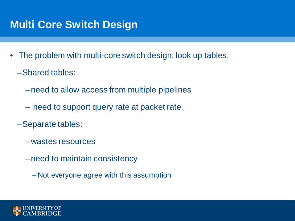
• The problem with multi-core switch design: look up tables.
–Shared tables:
–need to allow access from multiple pipelines
– need to support query rate at packet rate
–Separate tables:
–wastes resources
–need to maintain consistency
– Not everyone agree with this assumption
Multi Core Switch Design
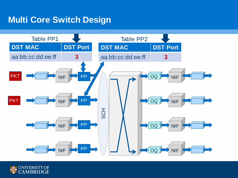
Multi Core Switch Design
PP
PP
PP
PP
NIF
NIF
NIF
NIF
NIF
NIF
NIF
NIF
OQ
OQ
OQ
OQ
SCH
PKT
PKT
DST MAC DST Portaa:bb:cc:dd:ee:ff 2DST MAC DST Portaa:bb:cc:dd:ee:ff 3
Table PP1DST MAC DST Portaa:bb:cc:dd:ee:ff 2DST MAC DST Portaa:bb:cc:dd:ee:ff 3
Table PP2
High Throughput Interfaces
Performance Limitations
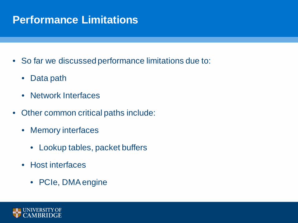
• So far we discussed performance limitations due to:
• Data path
• Network Interfaces
• Other common critical paths include:
• Memory interfaces
• Lookup tables, packet buffers
• Host interfaces
• PCIe, DMA engine
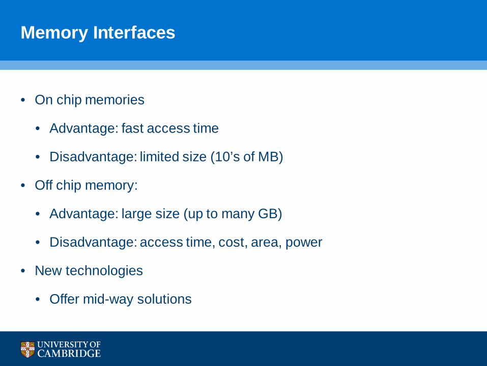
Memory Interfaces
• On chip memories
• Advantage: fast access time
• Disadvantage: limited size (10’s of MB)
• Off chip memory:
• Advantage: large size (up to many GB)
• Disadvantage: access time, cost, area, power
• New technologies
• Offer mid-way solutions

Example: QDR-IV SRAM
• Does 4 operations every clock: 2 READs, 2 WRITEs
• Constant latency
• Maximum random transaction rate: 2132 MT/s
• Maximum bandwidth: 153.3Gbps
• Maximum density: 144Mb
• Example applications: Statistics, head-tail cache, descriptors lists
Switch
QDR SRAM

Example: QDR-IV SRAM
• Does 4 operations every clock: 2 READs, 2 WRITEs• DDR4 DRAM: 2 operations every clock
• Constant latency• DDR4 DRAM: variable latency
• Maximum random transaction rate: 2132 MT/s• DDR4 DRAM: 20MT/s (worst case! tRC~50ns)
• DDR4 theoretical best case 3200MT/s• Maximum bandwidth: 153.3Gbps
• DDR4 DRAM maximum bandwidth: 102.4Gbps (for 32b (2x16) bus)• Maximum density: 144Mb
• DDR4 maximum density: 16Gb• Example applications: Statistics, head-tail cache, descriptors lists
• No longer applicable: packet buffer
Switch
QDR SRAM
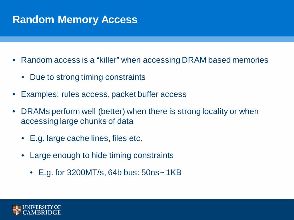
Random Memory Access
• Random access is a “killer” when accessing DRAM based memories
• Due to strong timing constraints
• Examples: rules access, packet buffer access
• DRAMs perform well (better) when there is strong locality or when accessing large chunks of data
• E.g. large cache lines, files etc.
• Large enough to hide timing constraints
• E.g. for 3200MT/s, 64b bus: 50ns~ 1KB
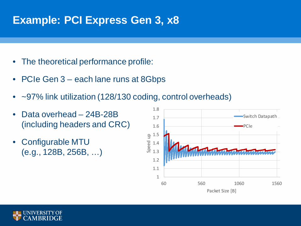
Example: PCI Express Gen 3, x8
• The theoretical performance profile:
• PCIe Gen 3 – each lane runs at 8Gbps
• ~97% link utilization (128/130 coding, control overheads)
• Data overhead – 24B-28B(including headers and CRC)
• Configurable MTU(e.g., 128B, 256B, …)
1
1.1
1.2
1.3
1.4
1.5
1.6
1.7
1.8
60 560 1060 1560
Spee
d up
Packet Size [B]
Switch Datapath
PCIe
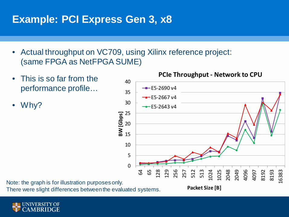
Example: PCI Express Gen 3, x8
• Actual throughput on VC709, using Xilinx reference project:(same FPGA as NetFPGA SUME)
• This is so far from the performance profile…
• Why?
0
5
10
15
20
25
30
35
40
64 65 128
129
256
257
512
513
1024
1025
2048
2049
4096
4097
8192
8193
1638
3
BW [G
bps]
Packet Size [B]
PCIe Throughput - Network to CPU
E5-2690 v4
E5-2667 v4
E5-2643 v4
Note: the graph is for illustration purposes only.There were slight differences between the evaluated systems.
Flow Control
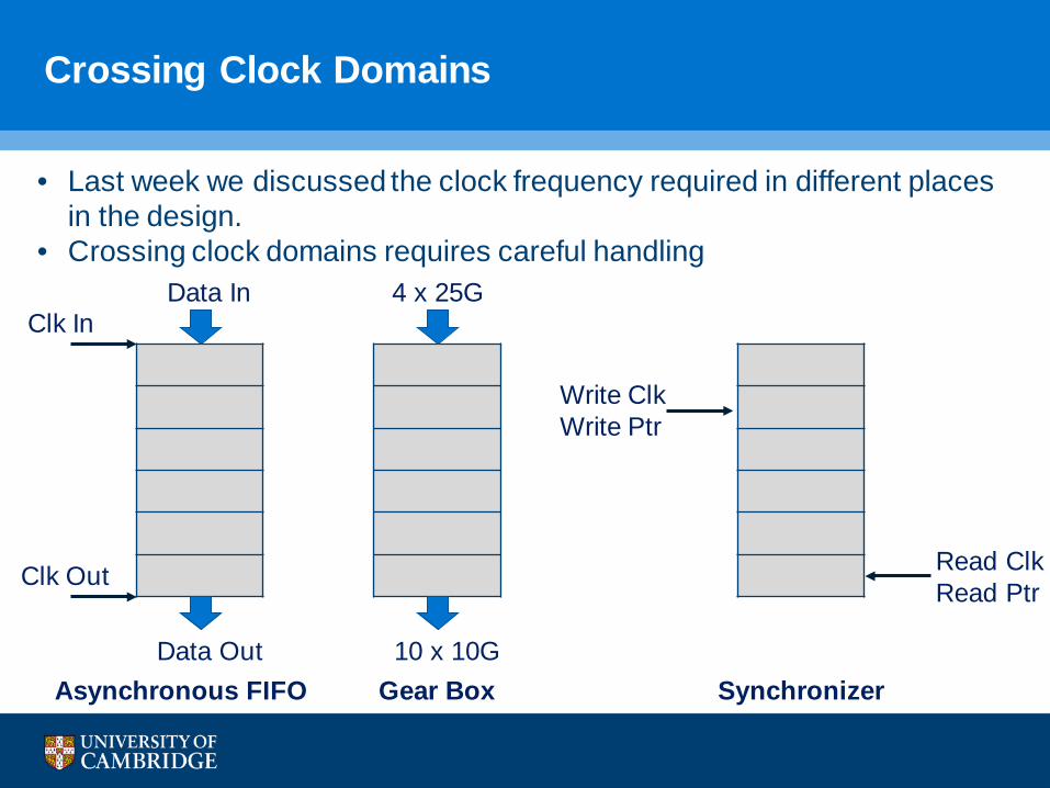
• Last week we discussed the clock frequency required in different places in the design.
• Crossing clock domains requires careful handling
Crossing Clock Domains
Data In
Data Out
Clk In
Clk Out
Asynchronous FIFO
4 x 25G
10 x 10GGear Box
Write ClkWrite Ptr
Read ClkRead Ptr
Synchronizer
• Why do we care about clock domain crossing?
• Adds latency
• The latency is not deterministic
• But bounded
• Crossing clock domains multiple times increases the jitter
• Using a single clock is often not an option:
• Insufficient packet processing rate
• Multiple interface clocks
• Need speed up (e.g., to handle control events)
Crossing Clock Domains

Flow Control
• The flow of the data through the device (the network) needs to be regulated
• Different events may lead to stopping the data:
• An indication from the destination to stop
• Congestion (e.g. 2 ports sending to 1 port)
• Crossing clock domains
• Rate control
• …
Data
Back pressure
Flow Control
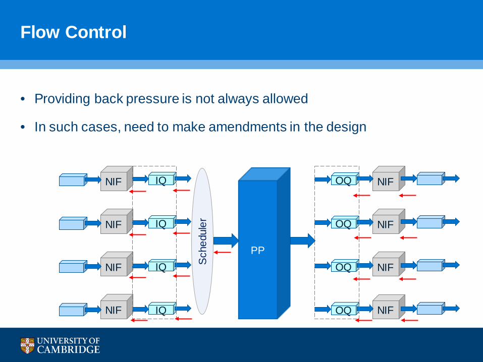
• Providing back pressure is not always allowed
• In such cases, need to make amendments in the design
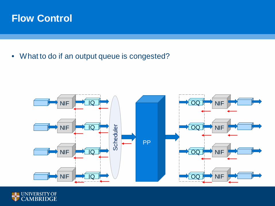
NIF
NIF
NIF
NIF
NIF
NIF
NIF
NIF
OQ
OQ
OQ
OQ
Sche
dule
r
PP
IQ
IQ
IQ
IQ
Flow Control
• What to do if an output queue is congested?
NIF
NIF
NIF
NIF
NIF
NIF
NIF
NIF
OQ
OQ
OQ
OQ
Sche
dule
r
PP
IQ
IQ
IQ
IQ
Flow Control and Buffering
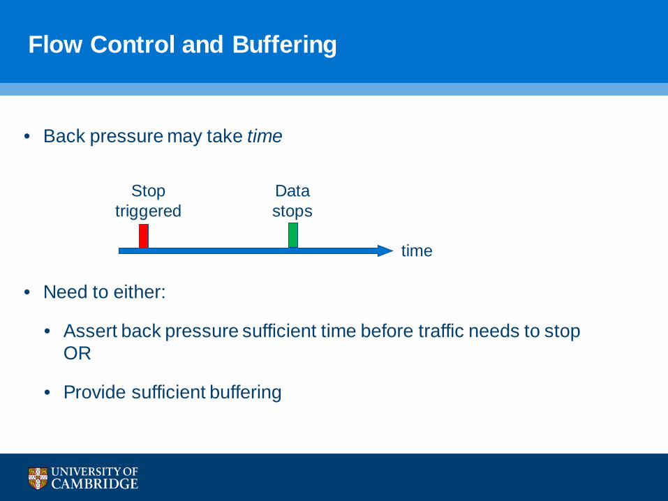
• Back pressure may take time
• Need to either:
• Assert back pressure sufficient time before traffic needs to stopOR
• Provide sufficient buffering
time
Datastops
Stoptriggered
Flow Control and Buffering
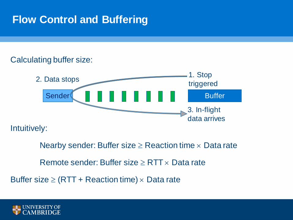
Calculating buffer size:
Intuitively:
Nearby sender: Buffer size ≥ Reaction time × Data rate
Remote sender: Buffer size ≥ RTT × Data rate
Buffer size ≥ (RTT + Reaction time) × Data rate
3. In-flight data arrives
2. Data stops 1. Stoptriggered
BufferSender

Flow Control and Buffering
Calculating buffer size:
2 switches, connected using 100m fibre, 10G port, instantaneous response time:Propagation delay in a fibre is 5ns/m
Buffer size ≥ 1us × 10Gbps = ~1.25KB
3. In-flight data arrives
2. Data stops 1. Stoptriggered
BufferSender
Low Latency Switches
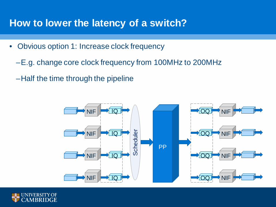
• Obvious option 1: Increase clock frequency
–E.g. change core clock frequency from 100MHz to 200MHz
–Half the time through the pipeline
How to lower the latency of a switch?
NIF
NIF
NIF
NIF
NIF
NIF
NIF
NIF
OQ
OQ
OQ
OQ
Sche
dule
r
PP
IQ
IQ
IQ
IQ

• Obvious option 1: Increase clock frequency
• Limitations:– Frequency is often a property of manufacturing process– Some modules (e.g. PCS) must work at a specific frequency (multiplications)
How to lower the latency of a switch?
NIF
NIF
NIF
NIF
NIF
NIF
NIF
NIF
OQ
OQ
OQ
OQ
Sche
dule
r
PP
IQ
IQ
IQ
IQ
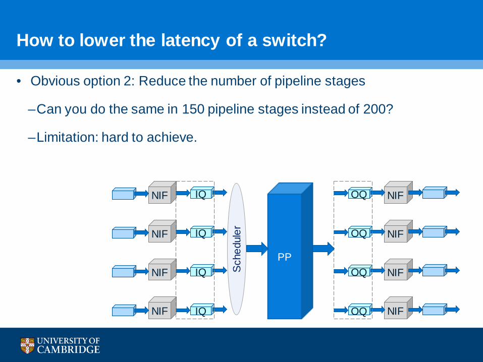
• Obvious option 2: Reduce the number of pipeline stages
–Can you do the same in 150 pipeline stages instead of 200?
–Limitation: hard to achieve.
How to lower the latency of a switch?
NIF
NIF
NIF
NIF
NIF
NIF
NIF
NIF
OQ
OQ
OQ
OQ
Sche
dule
r
PP
IQ
IQ
IQ
IQ
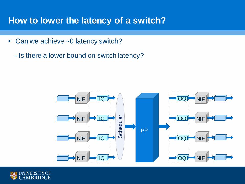
• Can we achieve ~0 latency switch?
–Is there a lower bound on switch latency?
How to lower the latency of a switch?
NIF
NIF
NIF
NIF
NIF
NIF
NIF
NIF
OQ
OQ
OQ
OQ
Sche
dule
r
PP
IQ
IQ
IQ
IQ


