+ All Categories
Home > Documents > p63x_en_m_bm6__610-611-620-621__vol_1__

p63x_en_m_bm6__610-611-620-621__vol_1__

Date post: 10-Jul-2015
Category:
Upload: jenny-huang
View: 564 times
Download: 16 times
Share this document with a friend
409
 MiCOM P631/P632/P633/P634 Transformer Differential Protection Devices P63x/EN M/Bm6 Version P631 -305/6/7/8 -403/4/5/6/7/8 -610/11/20/21 P632 -305/6/7/8 -403/4/5/6/7/8 -610/11/20/21 P633 -305/6/7/8 -404/5/6/7/8/9/10/11/12 -610/11/20/21 P634 -305/6/7/8 -403/4/5/6/7/8 -610/11/20/21 Technical Manual Content P63x/EN M/Ca4 (-610) P63x/EN AD/Ak6 (-611/620) P63x/EN AD/Am6 (-621) Volume 1 of 2
Transcript

7/11/2019 p63x_en_m_bm6__610-611-620-621__vol_1__

http://slidepdf.com/reader/full/p63xenmbm6610-611-620-621vol1 1/605

MiCOM

P631/P632/P633/P634Transformer Differential Protection Devices P63x/EN M/Bm6

VersionP631 -305/6/7/8 -403/4/5/6/7/8 -610/11/20/21

P632 -305/6/7/8 -403/4/5/6/7/8 -610/11/20/21P633 -305/6/7/8 -404/5/6/7/8/9/10/11/12 -610/11/20/21P634 -305/6/7/8 -403/4/5/6/7/8 -610/11/20/21

Technical Manual

Content P63x/EN M/Ca4 (-610)P63x/EN AD/Ak6 (-611/620)P63x/EN AD/Am6 (-621)

Volume 1 of 2

7/11/2019 p63x_en_m_bm6__610-611-620-621__vol_1__

http://slidepdf.com/reader/full/p63xenmbm6610-611-620-621vol1 2/605

7/11/2019 p63x_en_m_bm6__610-611-620-621__vol_1__

http://slidepdf.com/reader/full/p63xenmbm6610-611-620-621vol1 3/605

MiCOM

P631/P632/P633/P634Transformer Differential Protection Devices

P63x/EN M/Ca4(AFSV.12/09701 D)

Version P631 -305 -403/404 -610P632 -305 -403/404 -610

P633 -305 -404/405/406 -610P634 -305 -403/404 -610

Technical Manual

7/11/2019 p63x_en_m_bm6__610-611-620-621__vol_1__

http://slidepdf.com/reader/full/p63xenmbm6610-611-620-621vol1 4/605

7/11/2019 p63x_en_m_bm6__610-611-620-621__vol_1__

http://slidepdf.com/reader/full/p63xenmbm6610-611-620-621vol1 5/605

! Warning

When electrical equipment is in operation, dangerous voltage will be present in certain parts of theequipment. Failure to observe warning notices, incorrect use, or improper use may endanger personnel and equipment and cause personal injury or physical damage.

Before working in the terminal strip area, the device must be isolated. Where stranded conductorsare used, wire end ferrules must be employed.

Proper and safe operation of this device depends on appropriate shipping and handling, proper storage, installation and commissioning, and on careful operation, maintenance, and servicing.

For this reason only qualified personnel may work on or operate this device.

Any modifications to this device must be in accordance with the manual. If any other modificationis made without the express permission of Schneider Electric, it will invalidate the warranty, andmay render the product unsafe.

Qualified Personnel

are individuals who

are familiar with the installation, commissioning and operation of the device and of the system to which it is beingconnected;

are able to perform switching operations in accordance with safety engineering standards and are authorized toenergize and de-energize equipment and to isolate, ground, and label it;

are trained in the care and use of safety apparatus in accordance with safety engineering standards;

are trained in emergency procedures (first aid).

Note:

The operating manual for this device gives instructions for its installation, commissioning, and operation.However, the manual cannot cover all conceivable circumstances or include detailed information on all topics. Inthe event of questions or specific problems, do not take any action without proper authorization. Contact theappropriate Schneider Electric technical sales office and request the necessary information.

Any agreements, commitments, and legal relationships and any obligations on the part of Schneider Electric,including settlement of warranties, result solely from the applicable purchase contract, which is not affected by thecontents of the operating manual.

7/11/2019 p63x_en_m_bm6__610-611-620-621__vol_1__

http://slidepdf.com/reader/full/p63xenmbm6610-611-620-621vol1 6/605

7/11/2019 p63x_en_m_bm6__610-611-620-621__vol_1__

http://slidepdf.com/reader/full/p63xenmbm6610-611-620-621vol1 7/605

Modifications After Going to Press

P63X/EN M/Ba4 // AFSV.12.09701 D /// P631-305-403/404-610 // P632-305-403/404-610 // P633-305-404/405/406-610 // P634-305-403/404-610 11

7/11/2019 p63x_en_m_bm6__610-611-620-621__vol_1__

http://slidepdf.com/reader/full/p63xenmbm6610-611-620-621vol1 8/605

12 P63X/EN M/Ba4 // AFSV.12.09701 D /// P631-305-403/404-610 // P632-305-403/404-610 // P633-305-404/405/406-610 // P634-305-403/404-610

7/11/2019 p63x_en_m_bm6__610-611-620-621__vol_1__

http://slidepdf.com/reader/full/p63xenmbm6610-611-620-621vol1 9/605

Contents

P63X/EN M/Ba4 // AFSV.12.09701 D /// P631-305-403/404-610 // P632-305-403/404-610 // P633-305-404/405/406-610 // P634-305-403/404-610 13

1 Application and Scope 1-1

2 Technical Data 2-12.1 Conformity 2-12.2 General Data 2-12.3 Tests 2-22.3.1 Type tests 2-22.3.2 Routine Tests 2-52.4 Environmental Conditions 2-52.5 Inputs and Outputs 2-6

2.6 Interfaces 2-82.7 Information Output 2-112.8 Settings 2-112.9 Deviations 2-122.9.1 Deviations of the Operate Values 2-122.9.2 Deviations of the Timer Stages 2-132.9.3 Deviations of Measured Data Acquisition 2-142.10 Recording Functions 2-152.11 Power Supply 2-162.12 Current Transformer Specifications 2-17

7/11/2019 p63x_en_m_bm6__610-611-620-621__vol_1__

http://slidepdf.com/reader/full/p63xenmbm6610-611-620-621vol1 10/605

Contents(continued)

14 P63X/EN M/Ba4 // AFSV.12.09701 D /// P631-305-403/404-610 // P632-305-403/404-610 // P633-305-404/405/406-610 // P634-305-403/404-610

3 Operation 3-13.1 Modular Structure 3-13.2 Operator-Machine Communication 3-33.3 Configuration of the Measured

Value Panels(Function Group LOC) 3-4

3.4 Serial Interfaces 3-73.4.1 PC interface (Function Group PC) 3-73.4.2 Communication Interface (Function Group COMM1) 3-9

3.4.3 Communication Interface 2 (Function Group COMM2) 3-183.4.4 UCA2 Communication Interface (Function Group UCA2) 3-21

3.4.5 IEC 61850 CommunicationInterface (Function groups IEC,GOOSE and GSSE) 3-22

3.4.5.1 IEC 61850 CommunicationInterface

(Function Group IEC) 3-22

3.4.5.2 Generic Object OrientedSubstation Event

(Function Group GOOSE) 3.25

5.4.5.3 Generic Substation State Event (Function Group GSSE) 3-273.5 IRIG-B Clock Synchronization (Function Group IRIGB) 3-293.6 Configuration and Operating Mode

of the Binary Inputs(Function Group INP) 3-30

3.7 Measured data input (Function Group MEASI) 3-313.7.1 Direct Current Input 3-323.7.2 Input for Connection of a

Resistance Thermometer

3-36

3.8 Configuration, Operating Mode,and Blocking of the Output Relays

(Function Group OUTP) 3-37

3.9 Measured data output (Function Group MEASO) 3-403.9.1 BCD Measured Data Output 3-433.9.2 Analog Measured Data Output 3-453.9.3 Output of ‘External’ Measured

Data3-51

3.10 Configuration and Operating Modeof the LED Indicators

(Function Group LED) 3-52

3.11 Main Functions of the P63x (Function Group MAIN) 3-563.11.1 Conditioning of the Measured

values3-56

3.11.2 Phase Reversal Function 3-603.11.3 Selection of the Residual Current

to be Monitored3-62

3.11.4 Forming a Virtual Transformer End 3-643.11.5 Operating Data Measurement 3-663.11.6 Configuring and Enabling the

Protection Functions3-79

3.11.7 Activation of Dynamic Parameters 3-813.11.8 Multiple Blocking 3-823.11.9 Multiple Signaling of the

Measuring Circuit MonitoringFunction

3-84

3.11.10 Blocked / Faulty 3-85

3.11.11 Starting Signals and TrippingLogic

3-86

3.11.12 Time Tagging and ClockSynchronization

3-90

3.11.13 Resetting Mechanisms 3-92

7/11/2019 p63x_en_m_bm6__610-611-620-621__vol_1__

http://slidepdf.com/reader/full/p63xenmbm6610-611-620-621vol1 11/605

Contents(continued)

P63X/EN M/Ba4 // AFSV.12.09701 D /// P631-305-403/404-610 // P632-305-403/404-610 // P633-305-404/405/406-610 // P634-305-403/404-610 15

3.11.14 Assigning CommunicationsInterfaces to PhysicalCommunications Channels

3-93

3.11.15 Test mode 3-943.12 Parameter Subset Selection (Function Group PSS) 3-95

3.13 Self-Monitoring (Function Group SFMON) 3-973.14 Operating Data Recording (Function Group OP_RC) 3-1003.15 Monitoring Signal Recording (Function Group MT_RC) 3-1013.16 Overload Data Acquisition (Function Group OL_DA) 3-1023.17 Overload Recording (Function Group OL_RC) 3-1053.18 Fault Data Acquisition (Function Group FT_DA) 3-1083.19 Fault Recording (Function Group FT_RC) 3-1163.20 Differential Protection (Function Group DIFF) 3-122

3.21 Ground Differential Protection (Br:Restricted earth fault protection)

(Function Groups REF_1to REF_3)

3-145

3.22 Definite-Time OvercurrentProtection

(Function Groups DTOC1to DTOC3)

3-157

3.23 Inverse-Time OvercurrentProtection

(Function Groups IDMT1to IDMT3)

3-167

3-24 Thermal Overload Protection (Function Groups THRM1and THRM2)

3-183

3.25 Time-Voltage Protection (Function Group V<>) 3-1933.26 Over-/Underfrequency Protection (Function Group f<>) 3-1963.27 Overfluxing Protection (Function Group V/f) 3-2023.28 Current Transformer Supervision (Function Group CTS) 3-2103.29 Measuring-Circuit Monitoring (Function Groups MCM_1

to MCM_4)

3-218

3.30 Limit Value Monitoring (Function Group LIMIT) 3-2213.31 Limit Value Monitoring of Phase

Currents(Function Groups LIM_1 toLIM_3)

3-224

3.32 Programmable Logic (Function Group LOGIC) 3-227

7/11/2019 p63x_en_m_bm6__610-611-620-621__vol_1__

http://slidepdf.com/reader/full/p63xenmbm6610-611-620-621vol1 12/605

Contents(continued)

16 P63X/EN M/Ba4 // AFSV.12.09701 D /// P631-305-403/404-610 // P632-305-403/404-610 // P633-305-404/405/406-610 // P634-305-403/404-610

4 Design 4-14.1 Designs 4-14.2 Modules 4-9

5 Installation and Connection 5-15.1 Unpacking and Packing 5-15.2 Checking Nominal Data and Design Type 5-15.3 Location Requirements 5-25.4 Installation 5-35.5 Protective and Operational Grounding 5-145.6 Connection 5-155.6.1 Connecting Measuring and Auxiliary Circuits 5-15

5.6.2 Connecting the IRIG-B Interface 5-185.6.3 Connecting the Serial Interfaces 5-18

6 Local Control Panel 6-16.1 Display and Keypad 6-26.2 Changing between Display Levels 6-66.3 Display Illumination 6-76.4 Control at the Panel Level 6-76.5 Control at the Menu Tree Level 6-86.5.1 Navigation in the Menu Tree 6-86.5.2 Switching Between Address Mode and Plain Text Mode 6-96.5.3 Change-Enabling Function 6-106.5.4 Changing Parameters 6-13

6.5.5 Setting a List Parameter 6-146.5.6 Memory Readout 6-156.5.7 Resetting 6-196.5.8 Password-Protected Control Actions 6-206.5.9 Changing the Password 6-21

7 Settings 7-17.1 Parameters 7-17.1.1 Device Identification 7-27.1.2 Configuration Parameters 7-67.1.3 Function Parameters 7-507.1.3.1 Global 7-507.1.3.2 General Functions 7-557.1.3.3 Parameter Subsets 7-67

7/11/2019 p63x_en_m_bm6__610-611-620-621__vol_1__

http://slidepdf.com/reader/full/p63xenmbm6610-611-620-621vol1 13/605

Contents(continued)

P63X/EN M/Ba4 // AFSV.12.09701 D /// P631-305-403/404-610 // P632-305-403/404-610 // P633-305-404/405/406-610 // P634-305-403/404-610 17

8 Information and Control Functions 8-18.1 Operation 8-18.1.1 Cyclic Values 8-18.1.1.1 Measured Operating Data 8-18.1.1.2 Physical State Signals 8-88.1.1.3 Logic State Signals 8-158.1.2 Control and Testing 8-338.1.3 Operating Data Recording 8-378.2 Events 8-388.2.1 Event Counters 8-388.2.2 Measured Event Data 8-398.2.3 Event Recording 8-42

9 Commissioning 9-19.1 Safety Instructions 9-19.2 Commissioning Tests 9-3

10 Troubleshooting 10-1

11 Maintenance 11-1

12 Storage 12-1

13 Accessories and Spare Parts 13-1

14 Order Information 14-114.1 Order Information for P631 in 40TE case 14-114.2 Order Information for P632 in 40TE case 14-214.3 Order Information for P633 in 40TE or 84TE case 14-314.4 Order Information for P634 in 84TE case 14-4

AppendixA GlossaryB Signal ListC Terminal connection diagramsD Overview of Changes

Address list:See chapters 7, 8 and 10, as well as the MiCOM S1 / S&R-103support software.

7/11/2019 p63x_en_m_bm6__610-611-620-621__vol_1__

http://slidepdf.com/reader/full/p63xenmbm6610-611-620-621vol1 14/605

18 P63X/EN M/Ba4 // AFSV.12.09701 D /// P631-305-403/404-610 // P632-305-403/404-610 // P633-305-404/405/406-610 // P634-305-403/404-610

7/11/2019 p63x_en_m_bm6__610-611-620-621__vol_1__

http://slidepdf.com/reader/full/p63xenmbm6610-611-620-621vol1 15/605

1 Application and Scope

P63X/EN M/Ba4 // AFSV.12.09701 D /// P631-305-403/404-610 // P632-305-403/404-610 // P633-305-404/405/406-610 // P634-305-403/404-610 1-1

1 Application and Scope

The P63x differential protection devices are designed for the fast and selective short-circuit protection of transformers, motors and generators and of other two-, three- or four-winding end arrangements.

The MiCOM P63x range features fast three-stage differential protection by applying atripping characteristic with two knee points and two high value settable differentialcurrent thresholds to enable rapid tripping in conjunction with inrush, overfluxing andthrough-stabilization. Amplitude and vector group matching is made by just entering thenominal values of each transformer end and the associated current transformers.A new (optional) overreaching current measuring circuit monitoring function will preventunwanted tripping by differential protection for faults in the CT's secondary circuit.

When considering 1 ½ circuit breaker arrangements and ring busbar arrangements it isalso possible to define a virtual end, where phase currents and the residual current fromtwo freely-selectable ends may be added geometrically (vector sum).

A phase reversal function is available for applications in pumped storage power stations.

In a device type where protection functions are available more than once they may eachbe freely assigned to individual winding ends.

Moreover there are numerous backup protection and automatic control functionsavailable.

The relevant protection parameters can be stored in four independent parameter subsets in order to adapt the protection device to different operating and power systemmanagement conditions.

7/11/2019 p63x_en_m_bm6__610-611-620-621__vol_1__

http://slidepdf.com/reader/full/p63xenmbm6610-611-620-621vol1 16/605

Application and Scope(continued)

1-2 P63X/EN M/Ba4 // AFSV.12.09701 D /// P631-305-403/404-610 // P632-305-403/404-610 // P633-305-404/405/406-610 // P634-305-403/404-610

General functions General functions are complete function groups, which may be individually configured or cancelled, depending on the application (e.g. included in or excluded from the device’sconfiguration).An exception is the MA I N function, which is always visible.

A function is selected by a mouse click in the support software:

Unused or cancelled function groups are hidden to the user, thus simplifying the menu.

Communication functions and measured value functions may also be configured or excluded.

This concept provides a wide choice of functions and makes wide-ranging application of the protection device possible, with just one model version. On the other hand simpleand clear parameter settings and adaptations to each protection scheme can be made.The powerful programmable logic provided by the protection device also makes itpossible to accommodate special applications.

7/11/2019 p63x_en_m_bm6__610-611-620-621__vol_1__

http://slidepdf.com/reader/full/p63xenmbm6610-611-620-621vol1 17/605

Application and Scope(continued)

P63X/EN M/Ba4 // AFSV.12.09701 D /// P631-305-403/404-610 // P632-305-403/404-610 // P633-305-404/405/406-610 // P634-305-403/404-610 1-3

General Functions P631 P632 P633 P634

87 DIFF Differential protection

> Three-stage differential protection

> Amplitude and vector group matching

> Residual current filtering

> Tripping characteristic with two kneepoints

> Inrush stabilization

> Overfluxing stabilization

> Through stabilization

2 ends 2 ends 3 ends 4 ends

87 G REF_x Ground differential protection (Br:

Restricted earth fault protection)

- 2 3 3

50 DTOCx Definite-time overcurrent protection 2 2 3 3

51 IDMTx Inverse-time overcurrent protection 2 2 3 3

49 THRMx Thermal overload protection 1 1 2 2

27 / 59 V<> Time-voltage protection 1 1 1

81 O/U f<> Over-/underfrequency protection 1 1 1

24 U_f Overfluxing protection 1 1 1

CTS Current transformer supervision optional optional optional optional

MCM_x Measuring-circuit monitoring 2 2 3 4

LIMIT, LIM_x Limit value monitoring 2 2 3 3

LOGIC Programmable logic 1 1 1 1

Communication Functions P63x

COMM1, COMM2

IRIGB

IEC, GOOSE, GSSE

2 information interfaces

IRIG-B

IEC 61850 communications protocol

options

Input/output functions P631 P632 P633 P634

INP / OUTP Binary signal inputs / Output relays (maximum number) 4 / 14 34 / 22 40 / 30 34 / 22

Measured Value Functions P631 P632 P633 P634

MEASI / MEASO Analog input / output(20 mA and resistance thermometer inputs, 2 x 20 mAoutputs)

- optional optional optional

Measuring inputs P631 P632 P633 P634

Phase currents 2 x 3 2 x 3 3 x 3 4 x 3

Resultant current and neutral-point current - 2 3 3

Voltage - 1 1 1

7/11/2019 p63x_en_m_bm6__610-611-620-621__vol_1__

http://slidepdf.com/reader/full/p63xenmbm6610-611-620-621vol1 18/605

Application and Scope(continued)

1-4 P63X/EN M/Ba4 // AFSV.12.09701 D /// P631-305-403/404-610 // P632-305-403/404-610 // P633-305-404/405/406-610 // P634-305-403/404-610

Global functions In addition to the listed features and extensive self-monitoring, the P63x offers thefollowing global functions:

Global functions

PSS Parameter subset selection System measurements to support the user during commissioning, testingand operation

OP_RC Operating data recording(time-tagged event logging)

OL_DA Overload Data Acquisition

OL_RC Overload recording (time-tagged event logging) FT_DA Fault data acquisition for a particular, settable point in time during a fault FT_RC Fault recording (time-tagged event logging together with fault value

recording of the three phase currents, the residual currents, the threephase-to-ground voltages, the neutral-point displacement voltage and thereference voltage before, during and after a fault).

Further functions

Further functions

MAIN Main function DVICE Device

LED LED indicators LOC Local control panel PC PC link

SFMON Comprehensive self-monitoring MT_RC Monitoring Signal Recording

7/11/2019 p63x_en_m_bm6__610-611-620-621__vol_1__

http://slidepdf.com/reader/full/p63xenmbm6610-611-620-621vol1 19/605

Application and Scope(continued)

P63X/EN M/Ba4 // AFSV.12.09701 D /// P631-305-403/404-610 // P632-305-403/404-610 // P633-305-404/405/406-610 // P634-305-403/404-610 1-5

Functional diagram

Iph

V

IY,a

IY,b

Iph

IY,c

Iph

Iph

Ivirtual

Communication

to SCADA / Substation control / RTU / Modem ...via RS485 or Optical Fibre

using IEC 60870-5-101, -103, Modbus, DNP3, Courierresp.

via RJ45 or Fibre Optics using IEC 61850

Recordingand

DataAcquisition

Transformer Differential

Protection P63x

always available

optional or specific

Σ Σ Σ Σ Σ

COMM1 COMM2 IECInter

MiCOMIRIG-B Self

Monitoring

LIM-3 LIM-2 LIM-1 Metering

Overload rec.

Fault rec.

LOGIC

27, 59V<>

81f<>

24V/f

87GREF_3

87GREF_2

87GREF_1

50DTOC-3

50DTOC-2

50DTOC-1

51IDMT-3

51IDMT--2

51IDMT--1

49THRM2

49THRM1

87DIFF

RTD,mA mA_OP

BC_4

BC _3

BC_2

BC_1

7/11/2019 p63x_en_m_bm6__610-611-620-621__vol_1__

http://slidepdf.com/reader/full/p63xenmbm6610-611-620-621vol1 20/605

Application and Scope(continued)

1-6 P63X/EN M/Ba4 // AFSV.12.09701 D /// P631-305-403/404-610 // P632-305-403/404-610 // P633-305-404/405/406-610 // P634-305-403/404-610

Design The MiCOM P631, P632, P633 and P634 protection devices are modular in design.The plug-in modules are housed in a robust aluminum case and electricallyinterconnected via one analog p/c board and one digital p/c board.

Inputs and outputs The nominal current and voltage values of the measuring inputs on the P63x can be setwith the function parameters.

The nominal voltage range of the optical coupler inputs is 24 to 250 V DC. As an optionbinary signal input modules with a higher operate threshold are available.

The auxiliary voltage input for the power supply is also designed for an extended range.

The nominal voltage ranges are 48 to 250 V DC and 100 to 230 V AC. A 24 VDCversion is also available.

All output relays can be utilized for signaling and command purposes.

The optional PT 100 input is lead-compensated, balanced and linearized for PT 100resistance thermometers as per IEC 751.

The optional 0 to 20 mA input provides open-circuit and overload monitoring, zerosuppression defined by a setting, plus the option of linearizing the input variable via20 adjustable interpolation points.

Two selectable measured values (cyclically updated measured operating data andstored measured fault data) can be output as a burden-independent direct current viathe two optional 0 to 20 mA outputs. The characteristics are defined via 3 adjustableinterpolation points allowing a minimum output current (4 mA, for example) for slave-sideopen-circuit monitoring, knee-point definition for fine scaling, and a limitation to lower nominal currents (10 mA, for example). Where sufficient output relays are available,a selectable measured value can be output in BCD-coded form by contacts.

7/11/2019 p63x_en_m_bm6__610-611-620-621__vol_1__

http://slidepdf.com/reader/full/p63xenmbm6610-611-620-621vol1 21/605

Application and Scope(continued)

P63X/EN M/Ba4 // AFSV.12.09701 D /// P631-305-403/404-610 // P632-305-403/404-610 // P633-305-404/405/406-610 // P634-305-403/404-610 1-7

Control and display Local control panel

17 LED indicators,12 with user-definable functional assignment

PC interface

Communication interfaces (optional)

Information interfaces Information is exchanged through the local control panel, the PC interface, or twooptional communication interfaces (channel 1 and channel 2).

Using the first communication interface, the numerical protection device can be wired

either to the substation control system or to a telecontrol system.The first communication interface is optionally available with a switcheable protocol(per IEC 60870-5-103, IEC 870-5-101, DNP 3.0, MODBUS or Courier) or as anIEC 61850 interface.

The second communication interface (communication protocol per IEC 60870-5-103only) is designed for remote control.

External clock synchronization can be accomplished by using the optional IRIG-B input.

7/11/2019 p63x_en_m_bm6__610-611-620-621__vol_1__

http://slidepdf.com/reader/full/p63xenmbm6610-611-620-621vol1 22/605

Application and Scope(continued)

1-8 P63X/EN M/Ba4 // AFSV.12.09701 D /// P631-305-403/404-610 // P632-305-403/404-610 // P633-305-404/405/406-610 // P634-305-403/404-610

Overview of all function groups

P631 P632 P633 P634

IDMT1: Inverse-time overcurrent protection 1

IDMT2: Inverse-time overcurrent protection 2

IDMT3: Inverse-time overcurrent protection 3 - -

OUTP: Binary outputs

OP_RC: Operating data recording

DIFF: Differential protection

REF_1: Ground differential protection 1(Br: Restricted earth fault protection 1)

-

REF_2: Ground differential protection 2(Br: Restricted earth fault protection 2)

-

REF_3: Ground differential protection 3(Br: Restricted earth fault protection 3)

- -

INP: Binary input

f<>: Over-/underfrequency protection -

DVICE: Device

GOOSE: Generic Object Orientated Substation Events(as of P63x –610)

LIMIT: Limit value monitoring

MAIN: Main function

LIM_1: Limit value monitoring 1

LIM_2: Limit value monitoring 2

LIM_3: Limit value monitoring 3 - -

GSSE: IEC Generic Substation Status Events(as of P63x –610)

IEC: IEC 61850 Communication (as of P63x –610)

IRIGB: IRIG-B interface

COMM1: Communication interface 1

COMM2: Communication interface 2 (as of P63x –602)

LED: LED indicators

LOGIC: Logic

MEASO: Measured data output

MEASI: Measured data input

MCM_1: Measuring-circuit monitoring 1 (as of P63x –602)

MCM_2: Measuring-circuit monitoring 2 (as of P63x –602)

MCM_3: Measuring-circuit monitoring 3 (as of P63x –602)

MCM_4: Measuring-circuit monitoring 4 (as of P63x –602)

PC: PC link

PSS: Parameter subset selection

SFMON: Self-monitoring

CTS: Current transformer supervision (as of P63x –606)

FT_RC: Fault recording

FT_DA: Fault data acquisition

THRM1: Thermal overload protection 1

THRM2: Thermal overload protection 2 - -

V<>: Time-voltage protection -

V/f: Overfluxing protection (as of P63x –602)

OL_RC: Overload recording

OL_DA: Overload data acquisition

DTOC1: Definite-time overcurrent protection 1

DTOC2 Definite-time overcurrent protection 2

DTOC3: Definite-time overcurrent protection 3 - -

MT_RC: Monitoring signal recording

UCA2: Utility Communication Architecture 2.0(P63x –604/-605/-606 only)

LOC: Local control panel

7/11/2019 p63x_en_m_bm6__610-611-620-621__vol_1__

http://slidepdf.com/reader/full/p63xenmbm6610-611-620-621vol1 23/605

2 Technical Data

P63X/EN M/Ba4 // AFSV.12.09701 D /// P631-305-403/404-610 // P632-305-403/404-610 // P633-305-404/405/406-610 // P634-305-403/404-610 2-1

2 Technical Data

2.1 Conformity

Notice Applicable to P631 / P632 / P634, version -305 -403/404/-610 andP633 version -305-404/405/406-610.

Declaration of conformity (Per Article 10 of EC Directive 72/73/EC.)The products designated ‘P631, P632, P633 and P634 Transformer DifferentialProtection Devices’ have been designed and manufactured in compliance with Europeanstandards EN 60255-6 and EN 60010-1 and with the ‘EMC Directive’ and the ‘LowVoltage Directive’ issued by the Council of the European Community.

2.2 General Data

General device data Design Surface-mounted case suitable for wall installation or flush-mounted case for 19" cabinets and for control panels.

Installation PositionVertical ± 30°

Degree of ProtectionPer DIN VDE 0470 and EN 60529 or IEC 529.

IP 52; IP 20 for rear connection space with flush-mounted case(IP 10 for ring-terminal connection)

Weight40TE case: Approx. 7 kg; 84TE case: Approx. 11 kg

Dimensions and ConnectionsSee dimensional drawings (Chapter 4) and terminal connection diagrams (Chapter 5).

Terminals

PC interface (X6):EIA RS232 (DIN 41652) connector, type D-Sub, 9-pin.

Communication Interface:Optical fibers (X7 and X8): F-SMA optical fiber connection

per IEC 60874-2 and DIN 47258 (for plastic fibers)or optical fiber connection BFOC-ST

® connector 2.5

per IEC 60874-10-1 and DIN 47254-1 (for glass fibers)

(ST®

is a registered trademark of AT&TLightguide Cable Connectors)

or Leads (X9 and X10): M2 threaded terminal ends for wire cross-sections

up to 1.5 mm².

or (for IEC 61850 only via

100 Mbit/s Ethernet board) (X13): Glass fiber SC per IEC 60874-14-4 and RJ45 wire

IRIG-B Interface (X11): BNC plug.

7/11/2019 p63x_en_m_bm6__610-611-620-621__vol_1__

http://slidepdf.com/reader/full/p63xenmbm6610-611-620-621vol1 24/605

2 Technical Data(continued)

2-2 P63X/EN M/Ba4 // AFSV.12.09701 D /// P631-305-403/404-610 // P632-305-403/404-610 // P633-305-404/405/406-610 // P634-305-403/404-610

Current Measuring Inputs:Threaded terminals for pin-terminal connection: M5,self-centering with wire protection for conductor cross-sections ≤ 4 mm

2

or Threaded terminals for ring-terminal connection: M4

Other Inputs and Outputs:Threaded terminals for pin-terminal connection: M3,self-centering with wire protection for conductor cross-sections from 0.2 to 2.5 mm2 or Threaded terminals for ring-terminal connection: M4.

Creepage Distances and Clearances

Per EN 61010-1 and IEC 664-1.Pollution degree 3, working voltage 250 V,overvoltage category III, impulse test voltage 5 kV.

2.3 Tests

2.3.1 Type Tests

Type tests All tests per EN 60263-6

§or IEC 60255-26.

Electromagnetic compatibility (EMC)

Interference SuppressionPer EN 55022 § or IEC CISPR 22, Class A.

1 MHz Burst Disturbance TestPer IEC 255 Part 22-1

§or IEC 60255-22-1, Class III

Common-mode test voltage: 2.5 kVDifferential test voltage: 1.0 kVTest duration: > 2 s, Source impedance: 200 Ω

Immunity to Electrostatic DischargePer EN 60255-22-2

§or IEC 60255-22-2, severity level 3

Contact discharge, single discharges: > 10Holding time: > 5 s

Test voltage: 6 kVTest generator: 50 to 100 MΩ, 150 pF / 330 Ω

Immunity to Radiated Electromagnetic EnergyPer EN 61000-4-3

§and ENV 50204

§§, severity level 3

Antenna distance to tested device: > 1 m on all sidesTest field strength, frequency band 80 to 1000 MHz: 10 V / mTest using AM: 1 kHz / 80 %Single test at 900 MHz AM 200 Hz / 100 %

§For this EN, ENV or IEC standard, the DIN EN, DINV ENV or DIN IEC edition,

respectively, was used in the test.

7/11/2019 p63x_en_m_bm6__610-611-620-621__vol_1__

http://slidepdf.com/reader/full/p63xenmbm6610-611-620-621vol1 25/605

2 Technical Data(continued)

P63X/EN M/Ba4 // AFSV.12.09701 D /// P631-305-403/404-610 // P632-305-403/404-610 // P633-305-404/405/406-610 // P634-305-403/404-610 2-3

Electrical Fast Transient or Burst RequirementsPer IEC 60255-22-4, Class B.Power supply: Amplitude: 2 kV, Burst frequency: 5 kHzInputs and outputs: Amplitude: 2 kV, Burst frequency: 5 kHzCommunications: Amplitude: 1 kV, Burst frequency: 5 kHz

Per EN 61000-4-4§, severity level 4:

Power supply: Amplitude: 4 kV, Burst frequency: 2.5 kHz and 5 kHzInputs and outputs: Amplitude: 2 kV, Burst frequency: 5 kHzCommunications: Amplitude: 2 kV, Burst frequency: 5 kHz

Rise time of one pulse: 5 nsImpulse duration (50% value): 50 ns

Burst duration: 15 msBurst period: 300 msSource impedance: 50 W

Current/Voltage Surge Immunity Test Per EN 61000-4-5

§or IEC 61000-4-5, insulation class 4

Testing of circuits for power supply and asymmetrical or symmetrical lines.Open-circuit voltage, front time / time to half-value: 1.2 / 50 µsShort-circuit current, front time / time to half-value: 8 / 20 µsAmplitude: 4 / 2 kVPulse frequency: > 5 / minSource impedance: 12 / 42 Ω

Immunity to Conducted DisturbancesInduced by Radio Frequency Fields Per EN 61000-4-6 § or IEC 61000-4-6, severity level 3Test voltage: 10 V

Power Frequency Magnetic Field ImmunityPer EN 61000-4-8 § or IEC 61000-4-8, severity level 4Frequency: 50 HzTest field strength: 30 A / m

Alternating Component (Ripple) in DC Auxiliary Energizing QuantityPer IEC 255-1112 %

Insulation Voltage TestPer EN 61010-1 § and IEC 255-5.2 kV AC, 60 s.Only direct voltage (2.8 kV DC) must be used for the voltage test on the power supplyinputs. The PC interface must not be subjected to the voltage test.

Impulse Voltage Withstand TestPer IEC 255-5.Front time: 1.2 µsTime to half-value: 50 µs

Peak value: 5 kVSource impedance: 500 W

7/11/2019 p63x_en_m_bm6__610-611-620-621__vol_1__

http://slidepdf.com/reader/full/p63xenmbm6610-611-620-621vol1 26/605

2 Technical Data(continued)

2-4 P63X/EN M/Ba4 // AFSV.12.09701 D /// P631-305-403/404-610 // P632-305-403/404-610 // P633-305-404/405/406-610 // P634-305-403/404-610

Mechanical robustness 1(**)

Vibration TestPer EN 60255-21-1 § or IEC 255-21-1, test severity class 1Frequency range in operation: 10 to 60 Hz, 0.035 mm and 60 to 150 Hz, 0.5 gFrequency range during transport: 10 to 150 Hz, 1 g

Shock Response and Withstand Test, Bump TestPer EN 60255-21-2

§or IEC 255-21-2,

acceleration and pulse duration:Shock Response tests are carried out to verify full operability (during operation),test severity class 1 ,5 g for 11 ms,

Shock Withstand tests are carried out to verify the endurance (during transport),test severity class 1 ,15 g for 11 ms

Seismic Test Per EN 60255-21-3

§or IEC 60255-21-3, test procedure A, class 1

Frequency range:5 to 8 Hz, 3.5 mm / 1.5 mm, 8 to 35 Hz, 10 / 5 m/s2, 3 x 1 cycle.

Mechanical robustness 2(**)

Vibration TestPer EN 60255-21-1

§or IEC 255-21-1, test severity class 2

Frequency range in operation: 10 to 60 Hz, 0.075 mm and 60 to 150 Hz, 1.0 gFrequency range during transport: 10 to 150 Hz, 2 g

Shock Response and Withstand Test, Bump TestPer EN 60255-21-2

§or IEC 255-21-2,

acceleration and pulse duration:Shock Response tests are carried out to verify full operability (during operation),test severity class 2,10 g for 11 ms;Shock Withstand tests are carried out to verify the endurance (during transport),test severity class 1,15 g for 11 msShock bump tests are carried out to verify permanent shock (during transport),test severity class 1,10 g for 16 ms

Seismic TestPer EN 60255-21-3

§or IEC 60255-21-3, test procedure A, class 2

Frequency range:5 to 8 Hz, 7.5 mm / 3.5 mm, 8 to 35 Hz, 20 / 10 m/s2, 3 x 1 cycle.

(**)Mechanical robustness 2:Valid for with delivery date as of May 2005, if one of the following case variants isused:

Flush mounted case, flush-mounting method 2 (with angle brackets and frame)

Surface-Mounted Case

7/11/2019 p63x_en_m_bm6__610-611-620-621__vol_1__

http://slidepdf.com/reader/full/p63xenmbm6610-611-620-621vol1 27/605

2 Technical Data(continued)

P63X/EN M/Ca4 // AFSV.12.09701 D /// P631-305-403/404-610 // P632-305-403/404-610 // P633-305-404/405/406-610 // P634-305-403/404-610 2-5

2.3.2 Routine Tests

All tests per EN 60255-6§

or IEC 255-6and DIN 57435 Part 303.

Voltage TestPer IEC 255-52.2 kV AC, 1 s.Only direct voltage (2.8 kV DC) must be used for the voltage test on the power supplyinputs.The PC interface must not be subjected to the voltage test.

Additional Thermal Test

100% controlled thermal endurance test, inputs loaded.

2.4 Environmental Conditions

Environment

TemperaturesRecommended temperature range: -5°C to +55°C (23°F to 131°F)Storage and transit: -25 °C to +70 °C (-13 °F to +158 °F)

Ambient Humidity Range≤ 75 % relative humidity (annual mean),56 days at ≤ 95 % relative humidity and 40 °C (104°F), condensation not permitted.

Solar RadiationDirect solar radiation on the front of the device must be avoided.

7/11/2019 p63x_en_m_bm6__610-611-620-621__vol_1__

http://slidepdf.com/reader/full/p63xenmbm6610-611-620-621vol1 28/605

2 Technical Data(continued)

2-6 P63X/EN M/Ba4 // AFSV.12.09701 D /// P631-305-403/404-610 // P632-305-403/404-610 // P633-305-404/405/406-610 // P634-305-403/404-610

2.5 Inputs and Outputs

Measuring inputs CurrentRated current: 1 or 5 A AC (settable).Nominal burden per phase: < 0.13 VA at Inom

Load rating:continuous: 4 Inom

for 10 s: 30 Inom

for 1 s: 100 Inom

Nominal surge current: 250 Inom

VoltageNominal voltage Vnom: 50 to 130 V AC (adjustable)

Nominal burden per phase: < 0.3 VA at Vnom = 130 V AC

Load rating: continuous 150 V AC

Frequency Nominal frequency f nom: 50 Hz and 60 Hz (adjustable)

Operating range: 0.95 to 1.05 f nom

Frequency protection: 40 to 70 Hz

All other protection functions:Operating range: 0.95 to 1.05 f nom

Overfluxing protection: 0.5 to 1.5 f nom Binary signal inputs

Threshold Pickup and Drop-off Points as per Ordering Option18 V standard variant (VA,nom: = 24 to 250 V DC):

Switching threshold in the range 14 V to19 V

Special variant with switching thresholds from 58 to 72 % of the nominal supply voltage(i.e. definitively ,low’ for VA < 58 % of the nominal supply voltage,

definitively ,high’ for VA > 72 % of the nominal supply voltage)

"Special variant 73 V": Nominal supply voltage 110 V DC"Special variant 90 V": Nominal supply voltage 127 V DC"Special variant 146 V": Nominal supply voltage 220 V DC

"Special variant 155 V": Nominal supply voltage 250 V DC

Power consumption per inputStandard variant:VA = 19 ... 110 V DC: 0.5 W ± 30 %,

VA > 110 V DC: VA • 5 mA ± 30 %.

Special variant:Vin > Switching threshold: VA • 5 mA ± 30 %.

NotesThe standard variant of binary signal inputs (opto couplers) is recommended in mostapplications, as these inputs operate with any voltage from 19 V. Special versions with

higher pick-up/drop-off thresholds are provided for applications where a higher switchingthreshold is expressly required.

The maximum voltage permitted for all binary signal inputs is 300V DC.

7/11/2019 p63x_en_m_bm6__610-611-620-621__vol_1__

http://slidepdf.com/reader/full/p63xenmbm6610-611-620-621vol1 29/605

2 Technical Data(continued)

P63X/EN M/Ba4 // AFSV.12.09701 D /// P631-305-403/404-610 // P632-305-403/404-610 // P633-305-404/405/406-610 // P634-305-403/404-610 2-7

IRIG-B interface Minimum / maximum input voltage level(peak-peak): 100 mVpp / 20 Vpp.Input impedance: 33 kΩ at 1 kHz.Electrical isolation: 2 kV

Direct current input Input current: 0 to 26 mAValue range: 0.00 to 1.20 IDC,nom (IDC,nom = 20 mA)

Maximum permissible continuous current: 50 mAMaximum permissible input voltage: 17 VInput resistance: 100 Ω Open-circuit monitoring: 0 to 10 mA (adjustable)Overload monitoring: > 24.8 mAZero suppression: 0.000 to 0.200 IDC,nom (adjustable)

Resistance thermometer inputs

Resistance thermometer: For analog module, PT 100 permitted only.Mapping curve as per IEC 751.

§

Value range: -40.0 to +215.0°C3-wire configuration: max. 20 Ω per conductor.Open and short-circuited input permittedOpen-circuit monitoring: Θ > +215 °C and Θ < -40 °C

Output relays Rated voltage: 250 V DC, 250 V ACContinuous current: 5 AShort-duration current: 30 A for 0.5 sMaking capacity: 1000 W (VA) at L/R = 40 msBreaking capacity: 0.2 A at 220 V DC and L/R = 40 ms

4 A at 230 V AC and cosϕ = 0.4

BCD Measured Data Output

Maximum numerical value that can be displayed: 399

Direct Current Output

Value range: 0 to 20 mAPermissible load: 0 to 500 Ω Maximum output voltage: 15 V

7/11/2019 p63x_en_m_bm6__610-611-620-621__vol_1__

http://slidepdf.com/reader/full/p63xenmbm6610-611-620-621vol1 30/605

2 Technical Data(continued)

2-8 P63X/EN M/Ba4 // AFSV.12.09701 D /// P631-305-403/404-610 // P632-305-403/404-610 // P633-305-404/405/406-610 // P634-305-403/404-610

2.6 Interfaces

Local control panel Input or output:via seven keys and a 4 x 20 character-LCD display

State and fault signals:17 LED indicators (13 permanently assigned, 4 freely configurable)

PC interface Transmission rate: 300 to 115,200 baud (adjustable)

Communication interfaces

1 and 2 The communication module can be provided with up to two communication channels,depending on the module variant. Channel 1 is designed for twisted pair connection or fiber optic connection, whereas Channel 2 is intended for twisted pair connection only.

For communication interface 1, communication protocols based on IEC 60870-5-103,IEC 870-5-101, MODBUS or DNP 3.0 (as of version P63x -602 Courier) can be set.

Communication interface 2 can only be operated with the interface protocol based onIEC 60870-5-103.

For Wire LeadsPer RS 485 or RS 422, 2 kV isolationDistance to be bridgedPoint-to-point connection: max. 1200 mMultipoint connection: max. 100 m

Transmission rate Communication Protocol

BA-no. -910(one channel)

300 to 19,200 baud (adjustable) IEC 60870-5-103

BA-no. -921(two channels)

300 to 64,000 baud(adjustable for COMM1)

300 to 57,600 baud(adjustable for COMM2)

Can be set by user for onechannel

1) Distance to be bridged given for identical optical outputs and inputs at both ends, asystem reserve of 3 dB, and typical fiber attenuation.

7/11/2019 p63x_en_m_bm6__610-611-620-621__vol_1__

http://slidepdf.com/reader/full/p63xenmbm6610-611-620-621vol1 31/605

2 Technical Data(continued)

P63X/EN M/Ba4 // AFSV.12.09701 D /// P631-305-403/404-610 // P632-305-403/404-610 // P633-305-404/405/406-610 // P634-305-403/404-610 2-9

Plastic Fiber ConnectionOptical wavelength: typically 660 nmOptical output: min. -7.5 dBmOptical sensitivity: min. -20 dBmOptical input: max. -5 dBmDistance to be bridged:

1)max. 45 m

Transmission rate Communication Protocol

BA-no. -910(one channel)

300 to 38,400 baud (adjustable) IEC 60870-5-103

BA-no. -922

(two channels)

300 to 64,000 baud

(adjustable for COMM1)300 to 57,600 baud(adjustable for COMM2)

Can be set by user for one

channel

Glass Fiber Connection G 50/125Optical wavelength: typically 820 nmOptical output: min. -19.8 dBmOptical sensitivity: min. -24 dBmOptical input: max. -10 dBmDistance to be bridged:

1)max. 400 m

Glass Fiber Connection G 62.5/125

Optical wavelength: typically 820 nmOptical output: min. -16 dBmOptical sensitivity: min. -24 dBmOptical input: max. -10 dBmDistance to be bridged:1) max. 1,400 m

Glass Fiber Connection G 50/125 or G 62.5/125

Transmission rate Communication Protocol

BA-no. -910(one channel)

300 to 38,400 baud (adjustable) IEC 60870-5-103

BA-no. -924(two channels) 300 to 64,000 baud(adjustable for COMM1)300 to 57,600 baud

(adjustable for COMM2)

Can be set by user for onechannel

1)Distance to be bridged given for identical optical outputs and inputs at both ends, a

system reserve of 3 dB, and typical fiber attenuation.

7/11/2019 p63x_en_m_bm6__610-611-620-621__vol_1__

http://slidepdf.com/reader/full/p63xenmbm6610-611-620-621vol1 32/605

2 Technical Data(continued)

2-10 P63X/EN M/Ba4 // AFSV.12.09701 D /// P631-305-403/404-610 // P632-305-403/404-610 // P633-305-404/405/406-610 // P634-305-403/404-610

IRIG-B interface B122 formatAmplitude modulated signalCarrier frequency: 1 kHzBCD-coded variation data (daily)

Data transmission using the IEC 61850 protocol

Order ext. No. -936:Interface to connect a 100 Mbit/s Ethernet, glass fiber-SC and RJ45 wireor Order ext. No. -937:Interface to connect a 100 Mbit/s Ethernet, glass fiber-SC and RJ45 wire

For Wire Leadsper RJ45, 1.5 kV isolationDistance to be bridged: Max. 100 m

Glass Fiber Connection G 50/125Optical wavelength: typically 1300 nmOptical output: min. -23.5 dBmOptical sensitivity: min. -31 dBmOptical input: max. -14 dBm

Glass Fiber Connection G 62.5/125

Optical wavelength: typically 1300 nmOptical output: min. -20 dBmOptical sensitivity: min. -31 dBmOptical input: max. -14 dBm

The second communication interface (RS 485 connection, IEC 60870-5-103 protocol) isalso available.

7/11/2019 p63x_en_m_bm6__610-611-620-621__vol_1__

http://slidepdf.com/reader/full/p63xenmbm6610-611-620-621vol1 33/605

2 Technical Data(continued)

P63X/EN M/Ba4 // AFSV.12.09701 D /// P631-305-403/404-610 // P632-305-403/404-610 // P633-305-404/405/406-610 // P634-305-403/404-610 2-11

2.7 Information Output

Counters, measured data, signals and LED indications: see Chapter 8.

2.8 Settings

Typical characteristic data Main functionMinimum output pulse duration for a trip command: 0.1 to 10 s (adjustable)

Differential ProtectionOperate time at Id = 10 Idiff > with inrush restraint disabled, or at Id > Idiff >>>:

at least 13 ms, typically 15 ms.Operate time at Id = 2.5 Idiff > with inrush restraint disabled:at least 19 ms, typically 21 ms.Operate time at Id = 2.5 Idiff > with inrush restraint enabled:

at least 30 ms, typically 33 ms.

Definite-time and inverse-time overcurrent protectionOperate time including output relay (measured value from 0 to 2-fold operate value):

≤ 40 ms, approx. 30 msReset time (measured value drops from 2-fold operate value to 0):

≤ 40 ms, approx. 30 msStarting resetting ratio: Approx. 0.95

Time-Voltage ProtectionOperate time including output relay (measured value from nominal value to 1.2-foldoperate value or measured value from nominal value to 0.8-fold operate value):

≤ 40 ms, approx. 30 msReset time (measured value from 1.2-fold operate value to nominal valueor measured value from 0.8-fold operate value to nominal value):

≤ 45 ms, approx. 30 msResetting ratio for V<>: 1 to 10 % (adjustable)

Overfluxing protectionStarting and measurement resetting ratio (hysteresis): 0.95

7/11/2019 p63x_en_m_bm6__610-611-620-621__vol_1__

http://slidepdf.com/reader/full/p63xenmbm6610-611-620-621vol1 34/605

2 Technical Data(continued)

2-12 P63X/EN M/Ba4 // AFSV.12.09701 D /// P631-305-403/404-610 // P632-305-403/404-610 // P633-305-404/405/406-610 // P634-305-403/404-610

2.9 Deviations

2.9.1 Deviations of the Operate Values

Definitions Reference ConditionsSinusoidal signals at nominal frequency f nom, total harmonic distortion ≤ 2 %, ambient

temperature 20°C (68°F), and nominal auxiliary voltage VA,nom

DeviationDeviation relative to the setting under reference conditions.

Differential Protection Measuring systemDeviation for Idiff ≥: 0.2 Iref : ± 5 %

Harmonic blocking: ±10 %

Inrush Stabilization (Harmonic Restraint)Deviation: ± 10 %

Ground differential protection (Br: Restricted earth fault protection)

Measuring systemDeviation for Idiff ≥: 0.2 Iref : ± 5 %

Definite-time and inverse- time overcurrent protection

Deviation: ± 5 %

Thermal Overload Protection

Deviation: ± 5 %

Frequency protection Operate Valuesfnom = 50 Hz: Deviation: ± 30 mHzfnom = 60 Hz: Deviation: ± 40 mHz

df/dt protection Operate Valuesfnom = 50 Hz: Deviation: ± 0.1 Hz/sfnom = 60 Hz: Deviation: ± 0.1 Hz/s

Time-Voltage Protection Deviation: ± 3 %

Overfluxing protection Deviation: : ± 3 %

Direct current input Deviation: ± 1 %

Resistance thermometer Deviation: ± 2 ° or ± 1 %

7/11/2019 p63x_en_m_bm6__610-611-620-621__vol_1__

http://slidepdf.com/reader/full/p63xenmbm6610-611-620-621vol1 35/605

2 Technical Data(continued)

P63X/EN M/Ba4 // AFSV.12.09701 D /// P631-305-403/404-610 // P632-305-403/404-610 // P633-305-404/405/406-610 // P634-305-403/404-610 2-13

Analog Measured Data Output

Deviation: ± 1 %Output residual ripple with max. load: ± 1 %

2.9.2 Deviations of the Timer Stages

Definitions Reference Conditions Sinusoidal signals at nominal frequency f nom, total harmonic distortion ≤ 2 %, ambient

temperature 20 °C (68°F), and nominal auxiliary voltage VA,nom.

DeviationDeviation relative to the setting under reference conditions.

Definite-time stages Deviation: 1 % or + 20 ms to 40 ms

Inverse-time stages Deviation when I ≥ 2 Iref : ± 5 % + 10 to 25 ms

or for IEC 'Extremely Inverse', thermal overload and V/f characteristics:± 7.5 % + 10 to 20 ms

Limit Value Monitoring Limit Value Monitoring is not designed to be a high-speed protection function; it is used

for reporting purposes. This function is calculated approximately one time per second.Therefore, it is not accurate enough to provide meaningful data for the time deviation.

7/11/2019 p63x_en_m_bm6__610-611-620-621__vol_1__

http://slidepdf.com/reader/full/p63xenmbm6610-611-620-621vol1 36/605

2 Technical Data(continued)

2-14 P63X/EN M/Ba4 // AFSV.12.09701 D /// P631-305-403/404-610 // P632-305-403/404-610 // P633-305-404/405/406-610 // P634-305-403/404-610

2.9.3 Deviations of Measured Data Acquisition

Definitions Reference ConditionsSinusoidal signals at nominal frequency f nom, total harmonic distortion ≤ 2 %, ambient

temperature 20 °C (68°F), and nominal auxiliary voltage VA,nom.

DeviationDeviation relative to the setting under reference conditions.

Measured Operating Data Measuring Input CurrentsDeviation: ± 1 %

Measuring Input VoltageDeviation: ± 0.5 %

Internally formed restraining and differential currentsDeviation: ± 2 %

FrequencyDeviation: ± 10 mHz

Direct Current of Measured Data Input and OutputDeviation: ± 1 %

TemperatureDeviation: ± 2 °C

Fault data Phase and Star point currentsDeviation: ± 3 %

Restraining and Differential CurrentsDeviation: ± 5 %

Internal clock With free running internal clock:

Deviation: < 1 min/month

With external synchronization (with a synchronization interval ≤ 1 min):Deviation: < 10 ms

With synchronization via IRIG-B interface: ± 1 ms

7/11/2019 p63x_en_m_bm6__610-611-620-621__vol_1__

http://slidepdf.com/reader/full/p63xenmbm6610-611-620-621vol1 37/605

2 Technical Data(continued)

P63X/EN M/Ba4 // AFSV.12.09701 D /// P631-305-403/404-610 // P632-305-403/404-610 // P633-305-404/405/406-610 // P634-305-403/404-610 2-15

2.10 Recording Functions

Organization of the Recording Memories:

Operating data memory Scope for signals: All operation-relevant signals from a total of 1024 different

logic state signals

Depth: The 100 most recent signals

Monitoring signal memory Scope for signals: All signals relevant for self-monitoring from a total of

1024 different logic state signals

Depth: Up to 30 signals

Overload memory Number: The 8 most recent overload events

Scope for signals: All signals relevant for an overload event from a total of 1024 different logic state signals

Depth: 200 entries per overload event

Fault memory Number: The 8 most recent fault events

Scope for signals: Signals:All fault-relevant signals from a total of 1024 differentlogic state signals

Depth for fault values:Sampled values for all measured currents and voltages

Depth for signals Signals:200 entries per fault event

Depth for fault values:

Max. number of periods per fault set by the user; 820 periodsin total for all faults, that is 16.4 s (for f nom = 50 Hz) or 13.7 s

(for f nom = 60 Hz)

7/11/2019 p63x_en_m_bm6__610-611-620-621__vol_1__

http://slidepdf.com/reader/full/p63xenmbm6610-611-620-621vol1 38/605

2 Technical Data(continued)

2-16 P63X/EN M/Ba4 // AFSV.12.09701 D /// P631-305-403/404-610 // P632-305-403/404-610 // P633-305-404/405/406-610 // P634-305-403/404-610

Resolution of the Recorded Data

Signals Time resolution: 1 ms

Fault values Time resolution: 20 sampled values per period

Phase and Star point currents

Dynamic range: 33 Inom

Amplitude resolution at Inom = 1 A: 2 mA r.m.s.

at Inom = 5 A: 10.1 mA r.m.s.

Voltage Dynamic range: 150 V ACAmplitude resolution: 9.2 mVrms

2.11 Power Supply

Power supply Nominal auxiliary voltage VA,nom:

48 to 250 V DC and 100 to 230 V AC or 24 V DC(ordering option)

Operating range for direct voltage:0.8 to 1.1 VA,nom with a residual ripple of up to 12 % VA,nom

Operating range for alternating voltage: 0.9 to 1.1 VA,nom

Nominal burden where VA = 220 V DC and with maximum module configuration:

For case: 40TE 84TE

Relays de-energized,approx.:

13 W 13 W

Relays energizedapprox.:

29 W 37 W

Start-up peak current: < 3 A for duration of 0.25 msPermitted supply interruption: ≥ 50 ms for interruption of VA ≥ 220 V DC

7/11/2019 p63x_en_m_bm6__610-611-620-621__vol_1__

http://slidepdf.com/reader/full/p63xenmbm6610-611-620-621vol1 39/605

2 Technical Data(continued)

P63X/EN M/Ba4 // AFSV.12.09701 D /// P631-305-403/404-610 // P632-305-403/404-610 // P633-305-404/405/406-610 // P634-305-403/404-610 2-17

2.12 Current Transformer Specifications

The following equation is used to calculate the specifications of a current transformer for the offset maximum primary current:

( ) ( ) 'max1,iopnominomsat IkRRInRRV ⋅⋅+≥⋅⋅+=

with:Vsat: saturation voltage (IEC knee point)

I'1,max: non-offset maximum primary current, converted to the secondary side

Inom: rated secondary current

n: rated overcurrent factor

k: over-dimensioning factor Rnom: rated burden

Rop actual connected operating burden

Ri internal burden

The specifications of a current transformer can then be calculated for the minimumrequired saturation voltage Vsat as follows:

( ) 'max1,iopsat IkRRV ⋅⋅+≥

As an alternative, the specifications of a current transformer can also be calculated for the minimum required rated overcurrent factor n by specifying a rated power P

nom

as

follows:

( )( )

( )( ) nom

'max1,

inom

iop

nom

'max1,

inom

iop

I

Ik

PP

PP

I

Ik

RR

RRn ⋅⋅

+

+=⋅⋅

+

+≥

With

2nomii

2nomopop

2nomnomnom

IRP

IRP

IRP

⋅=

⋅=

⋅=

Theoretically, the specifications of the current transformer could be calculated for lack of saturation by inserting instead of the required over-dimensioning factor k its maximumvalue:

k Tmax ≈ +1 1ω

with:ω : system angular frequencyT1: system time constant

7/11/2019 p63x_en_m_bm6__610-611-620-621__vol_1__

http://slidepdf.com/reader/full/p63xenmbm6610-611-620-621vol1 40/605

2 Technical Data(continued)

2-18 P63X/EN M/Ba4 // AFSV.12.09701 D /// P631-305-403/404-610 // P632-305-403/404-610 // P633-305-404/405/406-610 // P634-305-403/404-610

However, this is not necessary. Instead, it is sufficient to calculate the over-dimensioning factor k such that the normal behavior of the analyzed protective functionis guaranteed under the given conditions.

The transformer differential protection device is equipped with a saturation discriminator.This function will generate a stabilizing blocking signal if a differential current occurs as aconsequence of transformer saturation with an external fault (in contrast to an internalfault). For the passing maximum fault current in the case of an external fault,overdimensioning is, therefore, obviated.

For the maximum fault current with an internal fault, static saturation up to a maximumsaturation factor ‘f S’ of 4 is permissible. This corresponds to an overdimensioning

factor ‘k’ of 0.25.

The implementation of these requirements is comparatively unproblematic astransformer differential protection would require overdimensioning in accordance with thetotal fault clearing time, which includes the total circuit-breaker open time for an externalfault.

Current transformers should observe the error limit values for class 5P.

7/11/2019 p63x_en_m_bm6__610-611-620-621__vol_1__

http://slidepdf.com/reader/full/p63xenmbm6610-611-620-621vol1 41/605

3 Operation

P63X/EN M/Ba4 // AFSV.12.09701 D /// P631-305-403/404-610 // P632-305-403/404-610 // P633-305-404/405/406-610 // P634-305-403/404-610 3-1

3 Operation

3.1 Modular Structure

The P63x, a numeric device, is part of the MiCOM P 30 family of devices. The devicetypes included in this family are built from identical uniform hardware modules.Figure 3-1 shows the basic hardware structure of the P63x.

3-1 Basic hardware structure

7/11/2019 p63x_en_m_bm6__610-611-620-621__vol_1__

http://slidepdf.com/reader/full/p63xenmbm6610-611-620-621vol1 42/605

3 Operation(continued)

3-2 P63X/EN M/Ba4 // AFSV.12.09701 D /// P631-305-403/404-610 // P632-305-403/404-610 // P633-305-404/405/406-610 // P634-305-403/404-610

The external analog and binary quantities – electrically isolated – are converted to theinternal processing levels by the peripheral modules T, Y, and X. Commands andsignals internally generated by the device are connected to the external plant viacontacts through the binary I/O modules X. The external auxiliary voltage is applied tothe power supply module V, which supplies the auxiliary voltages that are requiredinternally.

Analog data is transferred from the transformer module T via the analog bus module B tothe processor module P. The processor module contains all the elements necessary for the conversion of measured analog variables, including multiplexers and analog/digitalconverters. The analog data conditioned by the analog I/O module Y is transferred tothe processor module P via the digital bus module. Binary signals are fed to theprocessor module by the binary I/O modules X via the digital bus module.

The processor handles the processing of digitized analog variables and of binary signals,generates the protective trip and signals, and transfers them to the binary I/O modules Xvia the digital bus module. The processor module also handles overall devicecommunication. As an option, communication module A can be mounted on theprocessor module to provide serial communication with substation control systems.

The control and display elements of the integrated local control panel and the integratedPC interface are housed on control module L.

7/11/2019 p63x_en_m_bm6__610-611-620-621__vol_1__

http://slidepdf.com/reader/full/p63xenmbm6610-611-620-621vol1 43/605

3 Operation(continued)

P63X/EN M/Ba4 // AFSV.12.09701 D /// P631-305-403/404-610 // P632-305-403/404-610 // P633-305-404/405/406-610 // P634-305-403/404-610 3-3

3.2 Operator-Machine Communication

The following interfaces are available for the exchange of information between the user and the device:

Integrated local control panel (LOC)

PC interface

Communication interface

All settings and signals as well as all measurements and control functions are arrangedwithin the branches of the menu tree following a scheme that is uniform throughout thedevice family. The main branches are:

‘Parameters’ branch All settings are contained in this branch. This branch carries all settings, including thedevice identification data, the configuration parameters for adapting the device interfacesto the system, and the function parameters for adapting the device functions to theprocess. All values in this group are stored in non-volatile memory, which means thatthe values will be preserved even if the power supply fails.

‘Operation’ branch This branch includes all information relevant for operation such as measured operatingdata and binary signal states. This information is updated periodically and consequentlyis not stored. In addition, various controls are grouped here, for example those for resetting counters, memories and displays.

‘Events’ branch The third branch is reserved for the recording of events. All information in this group istherefore stored. In particular, the start/end signals during a fault, the measured faultdata, and the sampled fault waveforms are stored here and can be read out whenrequired.

Settings and signals are displayed either in plain text or as addresses, in accordancewith the user’s choice. Chapters 7, 8 and 10 describe the settings, signals andmeasured values available with the P63x. The possible setting values can be found inthe P63x's data model file associated with the PC operating program (MiCOM S1).

The configuration of the local control panel also permits the installation of MeasuredValue 'Panels’ on the LCD display. Different Panels are automatically displayed for specific system operating conditions. Priority increases from normal operation tooperation under overload conditions and finally to operation following a short circuit inthe system. Thus the P63x provides the measured data relevant for the prevailingconditions.

7/11/2019 p63x_en_m_bm6__610-611-620-621__vol_1__

http://slidepdf.com/reader/full/p63xenmbm6610-611-620-621vol1 44/605

3 Operation(continued)

3-4 P63X/EN M/Ba4 // AFSV.12.09701 D /// P631-305-403/404-610 // P632-305-403/404-610 // P633-305-404/405/406-610 // P634-305-403/404-610

3.3 Configuration of the Measured Value Panels (Function Group LOC)

The P63x offers Measured Value Panels, which display the measured values relevant ata given time.

During normal power system operation, the Operation Panel is displayed. As an eventoccurs, the display switches to the appropriate Event Panel - provided that measuredvalues have been selected for the Event Panels. In the event of overload event, thedisplay will automatically switch to the Operation Panel at the end of the event. In theevent of a fault, the Fault Panel remains active until the LED indicators or the faultmemories are reset.

Operation Panel

The Operation Panel is displayed after the set return time has elapsed, provided that atleast one measured value has been configured.

The user can select which of the measured operating values will be displayed on theOperation Panel by means of an ‘m out of n’ parameter. If more measured values areselected for display than the LC display can accommodate, then the display will switch tothe next set of values at intervals defined by the setting at LOC: Hold-Time for Panels or when the appropriate key on the local control panel is pressed.

3-2 Operation Panel

7/11/2019 p63x_en_m_bm6__610-611-620-621__vol_1__

http://slidepdf.com/reader/full/p63xenmbm6610-611-620-621vol1 45/605

3 Operation(continued)

P63X/EN M/Ba4 // AFSV.12.09701 D /// P631-305-403/404-610 // P632-305-403/404-610 // P633-305-404/405/406-610 // P634-305-403/404-610 3-5

Fault panel The Fault Panel is displayed in place of another data panel when there is a fault,provided that at least one measured value has been configured. The Fault Panelremains on display until the LED indicators or the fault memories are cleared.

The user can select the measured fault values that will be displayed on the Fault Panelby setting an 'm out of n' parameter. If more measured values are selected for displaythan the LC display can accommodate, then the display will switch to the next set of values at intervals defined by the setting at LO C: Hol d- Ti me for Pa ne ls or whenthe appropriate key on the local control panel is pressed.

3-3 Fault panel

7/11/2019 p63x_en_m_bm6__610-611-620-621__vol_1__

http://slidepdf.com/reader/full/p63xenmbm6610-611-620-621vol1 46/605

3 Operation(continued)

3-6 P63X/EN M/Ba4 // AFSV.12.09701 D /// P631-305-403/404-610 // P632-305-403/404-610 // P633-305-404/405/406-610 // P634-305-403/404-610

Overload Panel The Overload Panel is automatically displayed in place of another data panel when thereis an overload, provided that at least one measured value has been configured.The Overload Panel remains on display until the overload ends, unless a fault occurs.In this case the display switches to the Fault Panel.

The user can select the measured values that will be displayed on the Overload Panelby setting a 'm out of n' parameter. If more measured values are selected for displaythan the LC display can accommodate, then the display will switch to the next set of values at intervals defined by the setting at LO C: Hol d- Tim e fo r Pan el s or whenthe appropriate key on the local control panel is pressed.

3-4 Overload Panel

7/11/2019 p63x_en_m_bm6__610-611-620-621__vol_1__

http://slidepdf.com/reader/full/p63xenmbm6610-611-620-621vol1 47/605

3 Operation(continued)

P63X/EN M/Ba4 // AFSV.12.09701 D /// P631-305-403/404-610 // P632-305-403/404-610 // P633-305-404/405/406-610 // P634-305-403/404-610 3-7

3.4 Serial Interfaces

The P63x has a PC interface as a standard component. Communication module A isoptional and can be provided with one or two communication channels, depending onthe design version. Communication between the P63x and the control station’scomputer is through the communication module A. Setting and interrogation is possiblethrough all the P63x's interfaces.

If the communication module A with two communication channels is installed, settings for two communication interfaces will be available. The setting of communication interface 1(COMM1) may be assigned to the physical communication channels 1 or 2 (see section"Main Functions"). If the COMM1 settings have been assigned to communicationchannel 2, then the settings of communication interface 2 (COMM2) will automatically be

active for communication channel 1. Communications channel 2 can only be used totransmit data to and from the P63x if its PC interface has been de-activated. As soon asthe PC interface is used to transmit data, communications channel 2 becomes "dead".It will only be enabled again after the PC interface “Time-out ” has elapsed.

If tests are run on the P63x, the user is advised to activate the test mode. In this waythe PC or the control system will recognize all incoming test signals accordingly (seesection "Main Functions").

3.4.1 PC Interface (Function Group PC)

Communication between the device and a PC is through the PC interface. In order for data transfer between the P63x and the PC to function, several settings must be made inthe P63x.

There is a support software available as an accessory for P63x control (see Chapter 13).

7/11/2019 p63x_en_m_bm6__610-611-620-621__vol_1__

http://slidepdf.com/reader/full/p63xenmbm6610-611-620-621vol1 48/605

3 Operation(continued)

3-8 P63X/EN M/Ba4 // AFSV.12.09701 D /// P631-305-403/404-610 // P632-305-403/404-610 // P633-305-404/405/406-610 // P634-305-403/404-610

3-5 PC interface settings

7/11/2019 p63x_en_m_bm6__610-611-620-621__vol_1__

http://slidepdf.com/reader/full/p63xenmbm6610-611-620-621vol1 49/605

3 Operation(continued)

P63X/EN M/Ba4-S // AFSV.12.09701 D /// P631-305-403/404-610 // P632-305-403/404-610 // P633-305-404/405/406-610 // P634-305-403/404-610 3-9

3.4.2 Communication Interface (Function Group COMM1)

Communication between the P63x and the control station’s computer is done throughthe communication interface. Depending on the design version of communicationsmodule A (see "Technical Data") there are several interface protocols available.The IEC 60870-5-103 protocol is always supported. The following user-selectedinterface protocols are available for use with the P63x:

IEC 60870-5-103, "Transmission protocols - Companion standard for the informativeinterface of protection equipment, first edition, 1997-12 (corresponds to VDEW / ZVEIRecommendation, "Protection communication companion standard 1, compatibilitylevel 2", February 1995 edition) with additions covering control and monitoring

IEC 870-5-101, "Telecontrol equipment and systems - Part 5: Transmissionprotocols - Section 101 Companion standard for basic telecontrol tasks," first edition1995-11

ILS-C, internal protocol of Schneider Electric

MODBUS

DNP 3.0

COURIER

In order for data transfer to function properly, several settings must be made in the P63x.

Communication interface 1 can be blocked through a binary signal input. In addition,a signal or measured-data block can also be imposed through a binary signal input.

7/11/2019 p63x_en_m_bm6__610-611-620-621__vol_1__

http://slidepdf.com/reader/full/p63xenmbm6610-611-620-621vol1 50/605

3 Operation(continued)

3-10 P63X/EN M/Ba4 // AFSV.12.09701 D /// P631-305-403/404-610 // P632-305-403/404-610 // P633-305-404/405/406-610 // P634-305-403/404-610

3-6 Communication interface 1, selecting the interface protocol

7/11/2019 p63x_en_m_bm6__610-611-620-621__vol_1__

http://slidepdf.com/reader/full/p63xenmbm6610-611-620-621vol1 51/605

3 Operation(continued)

P63X/EN M/Ba4 // AFSV.12.09701 D /// P631-305-403/404-610 // P632-305-403/404-610 // P633-305-404/405/406-610 // P634-305-403/404-610 3-11

3-7 Communication interface 1, settings for the IEC 60870-5-103 interface protocol

7/11/2019 p63x_en_m_bm6__610-611-620-621__vol_1__

http://slidepdf.com/reader/full/p63xenmbm6610-611-620-621vol1 52/605

3 Operation(continued)

3-12 P63X/EN M/Ba4 // AFSV.12.09701 D /// P631-305-403/404-610 // P632-305-403/404-610 // P633-305-404/405/406-610 // P634-305-403/404-610

3-8 Communication interface 1, settings for the IEC 870-5-101 interface protocol

7/11/2019 p63x_en_m_bm6__610-611-620-621__vol_1__

http://slidepdf.com/reader/full/p63xenmbm6610-611-620-621vol1 53/605

3 Operation(continued)

P63X/EN M/Ba4 // AFSV.12.09701 D /// P631-305-403/404-610 // P632-305-403/404-610 // P633-305-404/405/406-610 // P634-305-403/404-610 3-13

3-9 Communication interface 1, settings for the ILS_C interface protocol

7/11/2019 p63x_en_m_bm6__610-611-620-621__vol_1__

http://slidepdf.com/reader/full/p63xenmbm6610-611-620-621vol1 54/605

3 Operation(continued)

3-14 P63X/EN M/Ba4 // AFSV.12.09701 D /// P631-305-403/404-610 // P632-305-403/404-610 // P633-305-404/405/406-610 // P634-305-403/404-610

3-10 Communication interface 1, settings for the MODBUS protocol

7/11/2019 p63x_en_m_bm6__610-611-620-621__vol_1__

http://slidepdf.com/reader/full/p63xenmbm6610-611-620-621vol1 55/605

3 Operation(continued)

P63X/EN M/Ba4 // AFSV.12.09701 D /// P631-305-403/404-610 // P632-305-403/404-610 // P633-305-404/405/406-610 // P634-305-403/404-610 3-15

3-11 Communication interface 1, settings for the DNP 3.0 protocol

7/11/2019 p63x_en_m_bm6__610-611-620-621__vol_1__

http://slidepdf.com/reader/full/p63xenmbm6610-611-620-621vol1 56/605

3 Operation(continued)

3-16 P63X/EN M/Ba4 // AFSV.12.09701 D /// P631-305-403/404-610 // P632-305-403/404-610 // P633-305-404/405/406-610 // P634-305-403/404-610

3-12 Communication interface 1, settings for the COURIER protocol

7/11/2019 p63x_en_m_bm6__610-611-620-621__vol_1__

http://slidepdf.com/reader/full/p63xenmbm6610-611-620-621vol1 57/605

3 Operation(continued)

P63X/EN M/Ba4 // AFSV.12.09701 D /// P631-305-403/404-610 // P632-305-403/404-610 // P633-305-404/405/406-610 // P634-305-403/404-610 3-17

Checking spontaneous signals

For interface protocols based on IEC 60870-5-103, IEC 870-5-101, or ILS_C it ispossible to select a signal for test purposes. The transmission of this signal to the controlstation as ‘sig. start‘ or ‘sig. end‘ can then be triggered via setting parameters.

3-13 Checking spontaneous signals

7/11/2019 p63x_en_m_bm6__610-611-620-621__vol_1__

http://slidepdf.com/reader/full/p63xenmbm6610-611-620-621vol1 58/605

3 Operation(continued)

3-18 P63X/EN M/Ba4 // AFSV.12.09701 D /// P631-305-403/404-610 // P632-305-403/404-610 // P633-305-404/405/406-610 // P634-305-403/404-610

3.4.3 Communication Interface 2 (Function Group COMM2)

Communication interface 2 supports the IEC 60870-5-103 interface protocol.

In order for data transfer to function properly, several settings must be made in the P63x.

7/11/2019 p63x_en_m_bm6__610-611-620-621__vol_1__

http://slidepdf.com/reader/full/p63xenmbm6610-611-620-621vol1 59/605

3 Operation(continued)

P63X/EN M/Ba4 // AFSV.12.09701 D /// P631-305-403/404-610 // P632-305-403/404-610 // P633-305-404/405/406-610 // P634-305-403/404-610 3-19

3-14 Settings for communication interface 2

7/11/2019 p63x_en_m_bm6__610-611-620-621__vol_1__

http://slidepdf.com/reader/full/p63xenmbm6610-611-620-621vol1 60/605

3 Operation(continued)

3-20 P63X/EN M/Ba4 // AFSV.12.09701 D /// P631-305-403/404-610 // P632-305-403/404-610 // P633-305-404/405/406-610 // P634-305-403/404-610

Checking spontaneous signals

It is possible to select a signal for test purposes. The transmission of this signal to thecontrol station as ‘sig. start‘ or ‘sig. end‘ can then be triggered via setting parameters.

Spontan.signal start

Spontan.signal end

3-15 Checking spontaneous signals

7/11/2019 p63x_en_m_bm6__610-611-620-621__vol_1__

http://slidepdf.com/reader/full/p63xenmbm6610-611-620-621vol1 61/605

3 Operation(continued)

P63X/EN M/Ba4 // AFSV.12.09701 D /// P631-305-403/404-610 // P632-305-403/404-610 // P633-305-404/405/406-610 // P634-305-403/404-610 3-21

3.4.4 UCA2 Communication Interface (Function Group UCA2)

This function group is available only with the P63x -604/-605/-606 device.

(As of device version P63x –610, the IEC 61850 communication interface is available:it uses function groups IEC, GOOSE and GSSE. A description is provided in thefollowing section).

The communication protocol ‘Utility Communication Architecture 2.0’ is implemented withthe UCA2 function group and the Ethernet module (in the 10 MHz and 100 MHzvariants).

Function group UCA2 is only available as an alternative to function group COMM1

(hardware ordering option!). Pending the implementation of the IEC 61850 protocol,the use of UCA2 is reserved for specific projects.

The UCA2 addresses for setting, information and control functions are described inchapters 7 and 8.

(See also the detailed description of the UCA2 protocol implementation:P54x_EN_UC_B42.pdf).

7/11/2019 p63x_en_m_bm6__610-611-620-621__vol_1__

http://slidepdf.com/reader/full/p63xenmbm6610-611-620-621vol1 62/605

3 Operation(continued)

3-22 P63X/EN M/Ba4 // AFSV.12.09701 D /// P631-305-403/404-610 // P632-305-403/404-610 // P633-305-404/405/406-610 // P634-305-403/404-610

3.4.5 IEC 61850 Communication Interface(Function groups IEC, GOOSE and GSSE)

These function groups are available only with the P63x -610 device.

The IEC 61850 communication protocol is implemented by these function groups and theEthernet module.

Note:

Function group IEC is only available as an alternative to function group COMM1(hardware ordering option!).

3.4.5.1 IEC 61850 Communication Interface (Function Group IEC)

IEC 61850 IEC 61850 was created jointly by users and manufacturers as an international standard.The main target of IEC 61850 is interoperability of devices. This includes the capabilityof two or more intelligent electronic devices (IED), manufactured by the same companyor different companies, to exchange data for combined operation.

Now this new communication standard IEC 61850 has created an open and commonbasis for communication from the process control level down to the network control level,for the exchange of signals, data, measured values and commands.

For a standardized description of all information and services available in a field device adata model, which lists all visible functions, is created. Such a data model, specificallycreated for each device, is used as a basis for an exchange of data between the devices

and all process control installations interested in such information. In order to facilitateengineering at the process control level a standardized description file of the device,based on XML, is created with the help of the data model. This file can be imported andprocessed further by the relevant configuration program used by the process controldevice. This makes possible an automated creation of process variables, substationsand signal images.

The following documentation with the description of the IEC 61850 data model, used withthe P63x, is available:

IDC file based on XML in the SCL (Substation Configuration Description Language)with a description of data, properties and services, available from the device, that areto be imported into the system configurator.

PICS_MICS_ADL file with the following contents:

PICS (Protocol Implementation Conformance Statement) with an overview of available services.

MICS (Model Implementation Conformance Statement) with an overview of available object types.

ADL (Address Assignment List) with an overview of the assignment of parameter addresses (signals, measuring values, commands, etc.) used by the device withthe device data model as per IEC 61850.

7/11/2019 p63x_en_m_bm6__610-611-620-621__vol_1__

http://slidepdf.com/reader/full/p63xenmbm6610-611-620-621vol1 63/605

3 Operation(continued)

P63X/EN M/Ba4 // AFSV.12.09701 D /// P631-305-403/404-610 // P632-305-403/404-610 // P633-305-404/405/406-610 // P634-305-403/404-610 3-23

Ethernet Module The optional Ethernet module provides an RJ45 connection and a fiber optic interfacewhere an Ethernet network can be connected. The selection which of the two interfacesis to be used to connect to the Ethernet network is made by setting the parameter I E C : E t h e rn e t m e d i a . The optical interface of the Ethernet module is currentlyavailable with an SC connector (100 Mbit/s and 1300 nm). A variant with an STconnector is being developed. The RJ45 connector supports 10 Mbit/s and 100 Mbit/s.

The optional Ethernet module additionally provides an RS485 interface for remoteaccess with the operating program MiCOM S1 (function group COMM2).

Notes: The P63x may only be equipped with the optional Ethernet module as analternative to the standard optional communication module. Therefore theEthernet based communication protocol IEC 61850 is only available as an

alternative to function group COMM1.

The Ethernet module can only be applied in conjunction with the processor module P (included in current hardware version) with the item number 9650135 or other processor modules available in the near future. When upgradingolder P63x hardware versions with an Ethernet module, which is technicallypossible, it must be kept in mind that such units are usually equipped with theprocessor module P, item number 0337 875. But this processor module Pdoes not support the Ethernet module and therefore the communicationsprotocol per IEC 61850 is also not supported. If such an upgrade is carriedout the processor module P must be exchanged. The processor module itemnumber can be checked by reading the device identification setting atD V I C E : M o d u l e v a r . s l o t 1 .

Activating and Enabling The IEC function group can be activated by setting the parameter I E C : Fu n c t i o ng r o up I EC . This parameter is only visible if the optional Ethernet communicationmodule is fitted to the device. After activation of IEC, all data points associated with thisfunction group (setting parameters, binary state signals etc.) become visible.The function can then be enabled or disabled by settingI E C : G e n e ra l e n a b l e U S E R .

The parameter settings for function groups IEC, GOOSE and GSSE in the device are notautomatically activated. Activation occurs either when the command I E C : E n ab l ec o n f i gu r a t i o n is executed or automatically when the device is switched online atM A I N : D e v i c e o n - l i n e .

Client Log-on Communication in Ethernet no longer occurs in a restrictive master slave system, as iscommon with other protocols. Instead server or client functionalities, as defined in the'Abstract Communication Service Interface' (ACSI, IEC 61870-7-2), are assigned to thedevices. A 'server' is always that device which provides information to other devices.A client may log-on to this server so as to receive information, for instance 'reports'.In a network a server can supply any number of clients with spontaneous or cyclicinformation.

In its function as server the P63x can supply up to 16 clients with information.

7/11/2019 p63x_en_m_bm6__610-611-620-621__vol_1__

http://slidepdf.com/reader/full/p63xenmbm6610-611-620-621vol1 64/605

3 Operation(continued)

3-24 P63X/EN M/Ba4 // AFSV.12.09701 D /// P631-305-403/404-610 // P632-305-403/404-610 // P633-305-404/405/406-610 // P634-305-403/404-610

Clock Synchronization With IEC 61850 clock synchronization occurs via the SNTP protocol, defined as standardfor Ethernet. Here the P63x functions as a SNTP client.

For clock synchronization one can select between the operating modes Broadcast fromSNTP Server or Request from Server . With the first operating mode synchronizationoccurs by a broadcast message sent from the SNTP server to all devices in the network,and in the second operating mode the P63x requests the device specific time signalduring a settable cycle.

Fault Transmission Transmission of fault files is supported per "File Transfer".

Transmission of "Goose

Messages" The so-called "Goose Message" is a particular form of data transmission. Whereasnormal server-client-services are transmitted at the MMS and TCP/IP level, the "GooseMessage" is transmitted directly at the Ethernet level with a high transmission priority.Furthermore these "Goose Messages" can be received by all participants in therespective sub-network, independent of their server or client function. In IEC 61850"Goose Messages" are applied for the accelerated transmission of information betweentwo or more devices. Application fields are, for example, a reverse interlocking, a transfer trip or a decentralized substation interlock. In future the "Goose Message" will thereforereplace a wired or serial protective interface.

According to IEC 61850 there are two types of "Goose Messages", GSSE andIEC-GOOSE. The GSSE is used to transmit binary information with a simpleconfiguration by 'bit pairs', and it is compatible with UCA2. However IEC-GOOSE

enables transmission of all data formats available in the data model, such as binaryinformation, integer values or even analog measured values. But this will require moreextensive configuration with the help of the data model from the field unit situated on theopposite side. With IEC-GOOSE the P63x at this time supports sending and receiving of binary information.

Communication with the Operating Program MiCOM S1 via the Ethernet Interface

Direct access by the operating program MiCOM S1 via the Ethernet interface on thedevice may occur through the "tunneling principle". Transmission is carried out by anEthernet Standard Protocol, but this is only supported by the associated operating

program MiCOM S1 (specific manufacturer solution). Such transmission isaccomplished over the same hardware for the network, which is used for server-clientcommunication and "Goose Messages".Available are all the familiar functions offered by the operating program MiCOM S1 suchas reading/writing of setting parameters or retrieving stored data.

The various settings, measured values and signals for function group IEC are describedin chapters 7 and 8.

7/11/2019 p63x_en_m_bm6__610-611-620-621__vol_1__

http://slidepdf.com/reader/full/p63xenmbm6610-611-620-621vol1 65/605

3 Operation(continued)

P63X/EN M/Ba4 // AFSV.12.09701 D /// P631-305-403/404-610 // P632-305-403/404-610 // P633-305-404/405/406-610 // P634-305-403/404-610 3-25

3.4.5.2 Generic Object Oriented Substation Event (Function Group GOOSE)

For high-speed exchange of information between individual IEDs (intelligent electronicdevices) in a local network, the P63x provides function group GOOSE (IEC-GOOSE) asdefined in the IEC 61850 standard. GOOSE features high-speed and securetransmission for trip commands, blocking, enabling, contact position signals and other signals.

"Goose Messages" are only transmitted by switches but not by routers. "GooseMessages" therefore remain in the local network to which the device is logged-on.

Activating and Enabling Function group GOOSE can be activated by setting the parameter

GO OS E : F un c t i on g r ou p GOOS E . This parameter is only visible if the optionalEthernet communication module is fitted to the device. After activation of GOOSE, alldata points associated to this function group (setting parameters, binary state signalsetc.) become visible.The function can then be enabled or disabled by settingG O O S E : G e n e ra l e n a b l e U S E R .

The parameter settings for function groups IEC, GOOSE and GSSE in the device are notautomatically activated. Activation occurs either when the commandI E C : E n ab l e c o n f i gu r a t i on is executed or automatically when the device isswitched online with M A I N : D e v i c e o n - l i ne . In addition function group IEC mustbe configured and enabled.

Sending GOOSE

With GOOSE the P63x can transmit up to 32 logic binary state signals. Selection of binary state signals is made by settingGO OS E : Ou t p u t n f c t . a s s i g . (n = 1 to 32). The assignment of data objectindexes to logic state signals is made in the range from 1 to 32 according to theassignment to GOOSE outputs.

GOOSE is automatically sent with each new state change of a configured binary statesignal or an external device. There are numerous send repetitions in fixed ascendingtime periods (10 ms, 20 ms, 50 ms, 100 ms, 500 ms, 1000 ms, 2000 ms). If after 2 seconds there is no further state change apparent, GOOSE is then sent cyclically at2-second intervals.

7/11/2019 p63x_en_m_bm6__610-611-620-621__vol_1__

http://slidepdf.com/reader/full/p63xenmbm6610-611-620-621vol1 66/605

3 Operation(continued)

3-26 P63X/EN M/Ba4 // AFSV.12.09701 D /// P631-305-403/404-610 // P632-305-403/404-610 // P633-305-404/405/406-610 // P634-305-403/404-610

In order to have unambiguous identification of GOOSE sent, characteristics such as theGoose ID number, MAC address, application ID and VLAN identifier must be enteredthrough parameter settings. Further characteristics are the 'Dataset ConfigurationRevision' with the fixed value "100" as well as the 'Dataset Reference', which is made upof the IED name (setting in function group IEC) and the fixed string"System/LLNO$GooseST".

GOOSE-DataSet: LLN0$GooseST

Goose ID: "Local IED"

Server nameSYSTEM/GosGGI01/Out1/stVal

Multicast MAC address: 01-0C-CD-01-00-00

VLAN Identifier: 0

GOOSE: Output 1 fct.assig.

… …

GOOSE: Output 2 fct.assig.

GOOSE: Output 32 fct.assig.

64Z6090A_EN

Server nameSYSTEM/GosGGI01/Out2/stVal

Server nameSYSTEM/GosGGI01/Out32/stVal

Identification:

Data range:

Application ID: 12288

DataSet Cfg. Revision: 100

DataSet Ref. : "Local IEDSystem/LLNO$GooseST"

VLAN Priority: 4

3-16 Basic structure of sent GOOSE

7/11/2019 p63x_en_m_bm6__610-611-620-621__vol_1__

http://slidepdf.com/reader/full/p63xenmbm6610-611-620-621vol1 67/605

3 Operation(continued)

P63X/EN M/Ba4 // AFSV.12.09701 D /// P631-305-403/404-610 // P632-305-403/404-610 // P633-305-404/405/406-610 // P634-305-403/404-610 3-27

With GOOSE up to 16 logic binary state signals can be received. Configuration of thelogic state signals received (GO OS E : I n p u t n f c t . as s i g . , where n = 1 to 16) ismade on the basis of the selection table of the binary inputs (opto coupler inputs).

For each state signal to be received from an external device the "Goose Message" mustbe selected that includes the information wanted by setting the Goose ID, the ApplicationID and the 'Dataset Reference'. With the further setting of the data object index and thedata attribute index through parameters, the required information from the chosenGOOSE will be selected. The device will not evaluate the identification features VLANidentifier and ‘Dataset Configuration Revision’ that are also included in the GOOSEreceived.

Each GOOSE includes time information on the duration of validity of its information.

This corresponds to the double time period to the next GOOSE repetition. If the durationof validity has elapsed without having received this GOOSE again (i.e. because of acommunications fault), the received signals will automatically be set to their respectivedefault values GOO SE : Inp ut n def au l t or GOO SE : Ext .D ev . n def au l t(n = 1 to 16).

The various settings, measured values and signals for function group GOOSE aredescribed in chapters 7 and 8.

3.4.5.3 Generic Substation State Event (Function Group GSSE)

For high-speed exchange of information between individual IEDs (intelligent electronicdevices) in a local network, the P63x provides, as an additional functionality, the function

group GSSE (UCA2.0-GOOSE) as defined in the IEC 61850 standard. GSSE featureshigh-speed and secure transmission of logic binary state signals such as trip commands,blocking, enabling and other signals.

Activating and Enabling Function Group GSSE can be activated by setting the parameter GS S E : F un c t i o ng r o up G SS E . This parameter is only visible if the optional Ethernet communicationmodule is fitted to the device. After activation of GSSE, all data points associated to thisfunction group (setting parameters, binary state signals etc.) become visible.The function can then be enabled or disabled by settingG S S E : G e n e ra l e n a b l e U S E R .

The parameter settings for function groups IEC, GOOSE and GSSE in the device are notautomatically activated. Activation occurs either when the command I E C : E n ab l ec o n f i gu r a t i on is executed or automatically when the device is switched online withMA I N : D ev i c e o n - l i ne . In addition the function group IEC must be configured andenabled.

7/11/2019 p63x_en_m_bm6__610-611-620-621__vol_1__

http://slidepdf.com/reader/full/p63xenmbm6610-611-620-621vol1 68/605

3 Operation(continued)

3-28 P63X/EN M/Ba4 // AFSV.12.09701 D /// P631-305-403/404-610 // P632-305-403/404-610 // P633-305-404/405/406-610 // P634-305-403/404-610

Sending GSSE With GSSE up to 32 logic binary state signals can be sent. Selection of binary statesignals is made by settingGS S E : O u t pu t n f c t . a s s i g . (n = 1 to 32). Each state signal selected is to beassigned to a bit pair in GSSE (GS S E : O u t pu t n b i t pa i r (n = 1 to 32)), whichwill transmit this state signal.

GSSE is automatically sent with each state change of a selected state signal. There willbe multiple send repetitions at ascending time periods. The first send repetition occursat the given cycle time set with the parameter G S S E : M i n . c y c l e . The cycles for the following send repetitions result from a conditional equation with the increment setwith the parameter GS S E : I n c r em en t . Should no further state changes occur up tothe time when the maximum cycle time has elapsed (GS S E : Ma x . c y c l e ) , thenGSSE will be sent cyclically at intervals as set for the max. cycle time.

In order to have unambiguous identification of a GSSE sent, the IED name is used whichwas set in function group IEC.

Receiving GSSE With GSSE up to 32 logic binary state signals can be received. Configuration of the logicbinary state signals received (GS S E : I n pu t n f c t . as s i g . , where n = 1 to 32) ismade on the basis of the selection table of the binary inputs (opto coupler inputs).

For each state signal to be received, the GSSE message, which will include the requiredinformation, must be selected by setting the IED name (GS SE : I E D n am e) .Selection of information wanted from the selected GSSE will occur by setting the bit pair (GSSE: b i t pa i r ) .

Each GSSE includes time information on the duration of validity of its information.This corresponds to the double time period to the next GSSE repetition. If the durationof validity has elapsed without having received this GSSE again (i.e. because of acommunications fault), the signals received will automatically be set to their respectivedefault value ( GS S E : I n pu t n d ef au l t (n = 1 to 32)).

The various settings, measured values and signals for function group GSSE aredescribed in chapters 7 and 8.

7/11/2019 p63x_en_m_bm6__610-611-620-621__vol_1__

http://slidepdf.com/reader/full/p63xenmbm6610-611-620-621vol1 69/605

3 Operation(continued)

P63X/EN M/Ba4 // AFSV.12.09701 D /// P631-305-403/404-610 // P632-305-403/404-610 // P633-305-404/405/406-610 // P634-305-403/404-610 3-29

3.5 IRIG-B Clock Synchronization (Function Group IRIGB)

If, for example, a GPS receiver with IRIG-B connection is available, the internal clock of the P63x can be synchronized to run on GPS time using the optional IRIG-B interface.It should be noted that the IRIG-B signal holds information on the day only (day of thecurrent year). Using this information and the year set at the P63x, the P63x calculatesthe current date (DD.MM.YY).

Disabling or enabling the IRIG-B interface

The IRIG-B interface can be disabled or enabled via a setting parameter.

Synchronization readiness

If the IRIG-B interface is enabled and receiving a signal, the P63x checks the receivedsignal for plausibility. Implausible signals are rejected by the P63x. If the P63x does notreceive a correct signal in the long run, synchronization will not be ready any longer.

3-17 IRIG-B interface

7/11/2019 p63x_en_m_bm6__610-611-620-621__vol_1__

http://slidepdf.com/reader/full/p63xenmbm6610-611-620-621vol1 70/605

3 Operation(continued)

3-30 P63X/EN M/Ba4 // AFSV.12.09701 D /// P631-305-403/404-610 // P632-305-403/404-610 // P633-305-404/405/406-

3.6 Configuration and Operating Mode of the Binary Inputs (Function Group INP)

The P63x has opto coupler inputs for processing binary signals from the substation.The functions that will be activated in the P63x by triggering these binary signal inputsare defined by the configuration of the binary signal inputs. The typical response time is< 10 ms, although for reliability it is recommended that the initiating signal is maintainedfor at least 30 ms.

Configuring the binary inputs

One function can be assigned to each binary signal input by configuration. The samefunction can be assigned to several signal inputs. Thus one function can be activatedfrom several control points having different signal voltages.

In this manual, we assume that the required functions (marked 'EXT' in the addressdescription) have been assigned to binary signal inputs by configuration.

It should be noted that time-critical applications such as time synchronization commandsshould not be mapped to the binary signal inputs of the analog I/O module as these havean increased reaction time due to internal processing.

Operating mode of the binary inputs

The operating mode for each binary signal input can be defined. The user can specifywhether the presence (active 'high' mode) or the absence (active 'low' mode) of avoltage should be interpreted as the logic '1' signal. The display of the state of a binary

signal input – 'low' or 'high' – is independent of the setting for the operating mode of thesignal input.

3-18 Configuration and operating mode of the binary signal inputs

7/11/2019 p63x_en_m_bm6__610-611-620-621__vol_1__

http://slidepdf.com/reader/full/p63xenmbm6610-611-620-621vol1 71/605

3 Operation(continued)

P63X/EN M/Ba4 // AFSV.12.09701 D /// P631-305-403/404-610 // P632-305-403/404-610 // P633-305-404/405/406-610 // P634-305-403/404-610 3-31

3.7 Measured Data Input (Function Group MEASI)

The P63x has a measured data input function involving two inputs. Direct current is fedto the P63x through one of the inputs. The other input is designed to connect aresistance thermometer.

The input current IDC is displayed as a measured operating value. The current that isconditioned for monitoring purposes (IDC,lin) is also displayed as a measured operatingvalue. In addition, it is monitored by the Limit Value Monitoring function to determinewhether it exceeds or falls below set thresholds (see "Limit Value Monitoring").

The measured temperature is also displayed as a measured operating value andmonitored by the limit value monitoring function to determine whether it exceeds or falls

below set thresholds (see "Limit Value Monitoring").

Disabling or enabling the measured data input function

The measured data input can be disabled or enabled via a setting parameter.

3-19 Disabling or enabling the measured data input function

7/11/2019 p63x_en_m_bm6__610-611-620-621__vol_1__

http://slidepdf.com/reader/full/p63xenmbm6610-611-620-621vol1 72/605

3 Operation(continued)

3-32 P63X/EN M/Ba4 // AFSV.12.09701 D /// P631-305-403/404-610 // P632-305-403/404-610 // P633-305-404/405/406-610 // P634-305-403/404-610

3.7.1 Direct Current Input

External measuring transducers normally supply an output current of 0 to 20 mA that isdirectly proportional to the physical quantity being measured – the temperature, for example.If the output current of the measuring transducer is directly proportional to the measuredquantity only in certain ranges, linearization can be arranged, provided that themeasured data input is set accordingly. Furthermore, for certain applications it may benecessary to limit the range being monitored or to monitor certain parts of the range witha higher or lower sensitivity. By setting the value pair MEASI: IDC x andME AS I: IDC, l in x, the user specifies which input current IDC will correspond to thecurrent that is monitored by the Limit Value Monitoring function, i.e., IDC,lin. The resultingpoints, called "interpolation points", are connected by straight lines in an IDC-IDC,lin

diagram. In order to implement a simple characteristic, it is sufficient to specify twointerpolation points, which are also used as limiting values (see figure 3-20). Up to20 interpolation points are available to implement a complex characteristic.When setting the characteristic the user must remember that only a monotonicallyincreasing curve is allowed (no peak or vee-shapes). If an invalid setting is entered, theSF MO N: In va li d s ca li ng ID C signal will be generated.

0

0.1

0.2

0.3

0.4

0.5

0.6

0.7

0.8

0.9

1

1.1

1.2

0 0.1 0.2 0.25 0.3 0.35 0.4 0.45 0.5 0.6 IDC/ IDC,nom

IDClin / IDC,nom

IDC1 IDC20

IDClin1

IDClin20

D5Z52KDA19Z5266A_EN

3-20 Example of the conversion of 4 to 10 mA input current to 0 to 20 mA monitored current, IDC,lin

7/11/2019 p63x_en_m_bm6__610-611-620-621__vol_1__

http://slidepdf.com/reader/full/p63xenmbm6610-611-620-621vol1 73/605

3 Operation(continued)

P63X/EN M/Ba4 // AFSV.12.09701 D /// P631-305-403/404-610 // P632-305-403/404-610 // P633-305-404/405/406-610 // P634-305-403/404-610 3-33

0

0.1

0.2

0.3

0.4

0.5

0.6

0.7

0.8

0 0.1 0.2 0.3 0.4 0.5 0.6 0.7 0.8 0.9 1 1.1 1.2

IDC / IDC,nom

IDClin / IDC,nom

D5Z52KEB

IDC1 IDC2 IDC3 IDC4 IDC20

IDC,lin1

IDC,lin2

IDC,lin3

IDC,lin4

IDC,lin20

Interpolation points

Enable IDC p.u.D5Z52KEB_EN

3-21 Example of a characteristic with five interpolation points (characteristic with zero suppression setting of 0.1 I DC,nom is shown as a broken

line)

Zero suppression Zero suppression is defined by setting M E A S I : E n ab l e I D C p . u . If the directcurrent does not exceed the set threshold, the per-unit input current IDC p.u. and the

current IDC,lin will be displayed as having a value of ‘ 0 ’.

Open-circuit and overload

monitoring The device is equipped with an open-circuit monitoring function. If current IDC falls belowthe set threshold, ME AS I: ID C< op en ci rc ui t, the M EA SI : Op en ci rc .20 m A i n p . signal is issued.

The input current is monitored in order to protect the 20 mA input against overloading.If it exceeds the fixed threshold of 24.8 mA, the M E A S I : O v e r l o ad 2 0m A i n pu tsignal is issued.

7/11/2019 p63x_en_m_bm6__610-611-620-621__vol_1__

http://slidepdf.com/reader/full/p63xenmbm6610-611-620-621vol1 74/605

3 Operation(continued)

3-34 P63X/EN M/Ba4 // AFSV.12.09701 D /// P631-305-403/404-610 // P632-305-403/404-610 // P633-305-404/405/406-610 // P634-305-403/404-610

3-22 Analog direct current input

7/11/2019 p63x_en_m_bm6__610-611-620-621__vol_1__

http://slidepdf.com/reader/full/p63xenmbm6610-611-620-621vol1 75/605

3 Operation(continued)

P63X/EN M/Ba4 // AFSV.12.09701 D /// P631-305-403/404-610 // P632-305-403/404-610 // P633-305-404/405/406-610 // P634-305-403/404-610 3-35

Beyond the linearization described above, the user has the option of scaling thelinearized values. Thereby negative values, for example, can be displayed as well andare available for further processing by protection functions.

3-23 Scaling of the linearized measured value

7/11/2019 p63x_en_m_bm6__610-611-620-621__vol_1__

http://slidepdf.com/reader/full/p63xenmbm6610-611-620-621vol1 76/605

3 Operation(continued)

3-36 P63X/EN M/Ba4 // AFSV.12.09701 D /// P631-305-403/404-610 // P632-305-403/404-610 // P633-305-404/405/406-610 // P634-305-403/404-610

3.7.2 Input for Connection of a Resistance Thermometer

This input is designed to connect a PT 100 resistance thermometer. The mappingcurve, R = f(T), of PT 100 resistance thermometers is defined in the IEC 751 standard.If the PT 100 resistance thermometer is connected using the 3-wire method, then nofurther calibration is required.

Open-circuit monitoring If there is an open measuring circuit due to a broken wire, the signal M E A S I : Op enci r c. PT 10 0 is issued.

3-24 Temperature measurement using a resistance thermometer

7/11/2019 p63x_en_m_bm6__610-611-620-621__vol_1__

http://slidepdf.com/reader/full/p63xenmbm6610-611-620-621vol1 77/605

3 Operation(continued)

P63X/EN M/Ba4 // AFSV.12.09701 D /// P631-305-403/404-610 // P632-305-403/404-610 // P633-305-404/405/406-610 // P634-305-403/404-610 3-37

3.8 Configuration, Operating Mode, and Blocking of the Output Relays(Function Group OUTP)

The P63x has output relays for the output of binary signals. The binary signalassignment is freely-configured by the user.

Configuration of the output relays

One binary signal can be assigned to each output relay. The same binary signal can beassigned to several output relays by configuration.

Operating mode of the output relays

The user can set an operating mode for each output relay that determines whether theoutput relay operates in a normally open arrangement (NO) or normally closedarrangement (NC) and whether it operates in latching mode. Latching can be disabledeither manually via a setting parameter, or by an appropriately configured binary signalinput, at the onset of a new fault or of a new system disturbance, depending on theselected operating mode.

Blocking the output relays The P63x offers the option of blocking all output relays via a setting parameter or by wayof an appropriately configured binary signal input. The output relays are likewiseblocked if the device is disabled via appropriately configured binary inputs.

In these cases the relays are treated according to their set operating mode, i.e. relays ina normally open arrangement (NO) are not tr iggered, whereas relays in a normallyclosed arrangement (NC) are triggered.

This does not apply to the relays associated with the signalsSFMON: Warning (relay) or MAIN: Blocked/faulty. Self-monitoring alarms arethus correctly indicated.

If the self-monitoring detects a serious hardware fault (see error messages in chapter 10,which will lead to a blocking of the protection), all output relays are reset regardless of the set operating mode or signal configuration.

7/11/2019 p63x_en_m_bm6__610-611-620-621__vol_1__

http://slidepdf.com/reader/full/p63xenmbm6610-611-620-621vol1 78/605

3 Operation(continued)

3-38 P63X/EN M/Ba4 // AFSV.12.09701 D /// P631-305-403/404-610 // P632-305-403/404-610 // P633-305-404/405/406-610 // P634-305-403/404-610

3-25 Configuration, setting the operating mode, and blocking the output relays

7/11/2019 p63x_en_m_bm6__610-611-620-621__vol_1__

http://slidepdf.com/reader/full/p63xenmbm6610-611-620-621vol1 79/605

3 Operation(continued)

P63X/EN M/Ba4 // AFSV.12.09701 D /// P631-305-403/404-610 // P632-305-403/404-610 // P633-305-404/405/406-610 // P634-305-403/404-610 3-39

Testing the output relays For testing purposes, the user can select an output relay and trigger it via a settingparameter. Therefore the device must be switched to 'off-line'. Triggering persists for the duration of the set hold time.

47Z1050A_EN

MAIN: Protectionenabled

No (off)

3-26 Testing the output relays

7/11/2019 p63x_en_m_bm6__610-611-620-621__vol_1__

http://slidepdf.com/reader/full/p63xenmbm6610-611-620-621vol1 80/605

3 Operation(continued)

3-40 P63X/EN M/Ba4 // AFSV.12.09701 D /// P631-305-403/404-610 // P632-305-403/404-610 // P633-305-404/405/406-610 // P634-305-403/404-610

3.9 Measured Data Output (Function Group MEASO)

Measured values made available by the P63x can be provided in BCD (binary codeddecimal) form through output relays or in analog form as direct current output. Output asdirect current can only occur if the device is equipped with analog module Y. BCDoutput is always possible, whether the device is equipped with analog module Y or not.

Disabling or enabling the measured data output function

The measured data output can be disabled or enabled via a setting parameter.

3-27 Disabling or enabling the measured data output function

7/11/2019 p63x_en_m_bm6__610-611-620-621__vol_1__

http://slidepdf.com/reader/full/p63xenmbm6610-611-620-621vol1 81/605

3 Operation(continued)

P63X/EN M/Ba4 // AFSV.12.09701 D /// P631-305-403/404-610 // P632-305-403/404-610 // P633-305-404/405/406-610 // P634-305-403/404-610 3-41

Enabling measured data output

The measured data output can be enabled through a binary signal input, provided thatthe function ME ASO : O ut p. en ab le d E XT has been configured. If the functionME AS O: Ou tp . en ab led EXT has not been configured to a binary signal input, thenthe measured data output is always enabled.

3-28 Enabling measured data output

7/11/2019 p63x_en_m_bm6__610-611-620-621__vol_1__

http://slidepdf.com/reader/full/p63xenmbm6610-611-620-621vol1 82/605

3 Operation(continued)

3-42 P63X/EN M/Ba4 // AFSV.12.09701 D /// P631-305-403/404-610 // P632-305-403/404-610 // P633-305-404/405/406-610 // P634-305-403/404-610

Resetting the measured data output function

BCD or analog output of measured values is terminated for the duration of the hold timeif one of the following conditions is met:

The measured data output is reset either via a setting parameter or via anappropriately configured binary signal input.

There is a general reset.

LED indicators reset

3-29 Resetting the measured data output function

Scaling Scaling is used to map the physical measuring range to the device's inherent settingrange.

7/11/2019 p63x_en_m_bm6__610-611-620-621__vol_1__

http://slidepdf.com/reader/full/p63xenmbm6610-611-620-621vol1 83/605

3 Operation(continued)

P63X/EN M/Ba4 // AFSV.12.09701 D /// P631-305-403/404-610 // P632-305-403/404-610 // P633-305-404/405/406-610 // P634-305-403/404-610 3-43

3.9.1 BCD Measured Data Output

The user can select a measured value for output in BCD form by assigning output relays.

The selected measured value is available in BCD form for the duration of the set holdtime ME AS O: Hol d T im e O ut pu t BC D. If the selected variable was not measured,then there is no output of a measured value.

Output of measured event values

If the measured event value is updated during the hold time, the measured value outputmemory is cleared and the hold time is re-started. This leads to an immediate availabilityat the output of the updated value.

Output of measured operating values

The selected measured operating value is available for the duration of the set hold time.After the hold time has elapsed, the current value is saved and the hold time is re-started. If the hold time has been set to 'blocked ', the measured operating value that hasbeen output will be stored until the measured data output function is reset.

Scaling of BCD output The resolution for measured data output is defined by setting the scaling factor.The scaling factor should be selected so that the value 399 is not exceeded by themaximum measured value to be output. If this should occur or if the measured value isoutside the acceptable measuring range, then the value for "Overflow" (all relaystriggered) is transmitted.

factor scaling

MM max,x

scal,x =

where:

scal,xM : scaled measured value

Mx,max : maximum transmitted value for the selected measured value

7/11/2019 p63x_en_m_bm6__610-611-620-621__vol_1__

http://slidepdf.com/reader/full/p63xenmbm6610-611-620-621vol1 84/605

3 Operation(continued)

3-44 P63X/EN M/Ba4 // AFSV.12.09701 D /// P631-305-403/404-610 // P632-305-403/404-610 // P633-305-404/405/406-610 // P634-305-403/404-610

3-30 BCD Measured Data Output

7/11/2019 p63x_en_m_bm6__610-611-620-621__vol_1__

http://slidepdf.com/reader/full/p63xenmbm6610-611-620-621vol1 85/605

3 Operation(continued)

P63X/EN M/Ba4 // AFSV.12.09701 D /// P631-305-403/404-610 // P632-305-403/404-610 // P633-305-404/405/406-610 // P634-305-403/404-610 3-45

3.9.2 Analog Measured Data Output

Analogue output of measured data is two-channel.

The user can select two of the measured values available in the P63x for output in theform of load-independent direct current. Three interpolation points per channel can bedefined for specific adjustments such as adjustment to the scaling of a measuringinstrument. The direct current that is output is displayed as a measured operating value.

The selected measured value is output as direct current for the duration of the set holdtime ME AS O: Ho ld t ime ou tpu t A- x. If the selected variable was not measured,then there is no output of a measured value.

Output of measured event values

If the measured event value is updated during the hold time, the measured value outputmemory is cleared and the hold time is re-started. This leads to an immediate availabilityat the output of the updated value.

Output of measured operating values

The selected measured operating value is available for the duration of the set hold time.After the hold time has elapsed, the current value is saved and the hold time isre-started. If the hold time has been set to "blocked ", the measured operating value thathas been output will be stored until the measured data output function is reset.

Configuration of output relays assigned to the output channels

The user must keep in mind that direct current output only occurs when the output relaysassigned to the output channels are configured for ME ASO : Val ue A-x ou tpu t ,since the output channels would otherwise remain short-circuited (see terminalconnection diagrams).

7/11/2019 p63x_en_m_bm6__610-611-620-621__vol_1__

http://slidepdf.com/reader/full/p63xenmbm6610-611-620-621vol1 86/605

3 Operation(continued)

3-46 P63X/EN M/Ba4 // AFSV.12.09701 D /// P631-305-403/404-610 // P632-305-403/404-610 // P633-305-404/405/406-610 // P634-305-403/404-610

Scaling the analog display In order to define the resolution for measured data output the measured value range inscaled form and the associated display range have to be set. One additional value for the knee point must also be defined. In this way the user can obtain an analog outputcharacteristic similar to the characteristic shown in Figure 3-31.

Measured value range to be output

The measured value range to be output is (Mx,min ... Mx,knee ... Mx,max),with:Mx,min: minimum value to be outputMx,knee: Knee point value for the measured value range to be outputMx,max: maximum value to be output

This measured value range to be output is defined by setting the following parameters:

M E A S O : S c a l e d m i n . v a l . A - x

M E A S O : S c a l e d k n e e v a l . A - x

M E A S O : S c a l e d m a x . v a l . A - x

Scaling is made with reference to the complete range of values for the selectedmeasured value (variable Mx). The complete range of values is defined by their endvalues Mx,RL1 and Mx,RL2. (Mx,RL1 and Mx,RL2 are listed in the S&R-103 - PC MiCOM S1Support Software - under "minimum" and "maximum".)

Measured values Range

Measured values of thevariable Mx

Mx,RL1 ... Mx,RL2

Associated scaled measuredvalues

0 ... 1

Measured value to beoutput

Range

Measured values with knee-point to be output

Mx,min ... Mx,knee ... Mx,max

Scaled measured values

with a scaled knee-point tobe output

Mx,scal,min ... Mx,scal,knee ... Mx,scal,max

with:

Mx,scal,min = (Mx,min - Mx,RL1) / (Mx,RL2 - Mx,RL1

Mx,scal,knee = (Mx,knee - Mx,RL1) / (Mx,RL2 - Mx,RL1)

Mx,scal,max = (Mx,max - Mx,RL1) / (Mx,RL2 - Mx,RL1

Designation of the setvalues in the data model

"Scal. min. value Ax" ...... "Scal. knee-point Ax" ...

... "Scal. max. value Ax"

7/11/2019 p63x_en_m_bm6__610-611-620-621__vol_1__

http://slidepdf.com/reader/full/p63xenmbm6610-611-620-621vol1 87/605

3 Operation(continued)

P63X/EN M/Ba4 // AFSV.12.09701 D /// P631-305-403/404-610 // P632-305-403/404-610 // P633-305-404/405/406-610 // P634-305-403/404-610 3-47

Associated display range The associated display range is defined by setting the following parameters:

M E A S O : A n O u t m i n . v a l . A - x

M E A S O : A n O u t k n e e p o i n t A - x

M E A S O : A n O u t m a x . v a l . A - x

Measured values Analog display values

Measured values in therange "Measured values tobe output"

"AnOut min. val. A-x" ...... "AnOut knee point A-x" ...

...

... "AnOut max. val. A-x"(Value A-x valid)

Measured values:Mx,RL1 = Mx = Mx,min

"AnOut min. val." (Value A-x not valid)

Measured values Mx:Mx,max = Mx = Mx,RL2

"AnOut max. val." (Value A-x not valid)

Measured values Mx:Mx < Mx,RL1or Mx > Mx,RL2

"AnOut max. val." (Overflow)

7/11/2019 p63x_en_m_bm6__610-611-620-621__vol_1__

http://slidepdf.com/reader/full/p63xenmbm6610-611-620-621vol1 88/605

3 Operation(continued)

3-48 P63X/EN M/Ba4 // AFSV.12.09701 D /// P631-305-403/404-610 // P632-305-403/404-610 // P633-305-404/405/406-610 // P634-305-403/404-610

Example for scaling of analog display ranges

Voltage A-B is selected as the measured value to be transmitted by channel A-1.The measuring range is from 0 to 1.5 Vnom with Vnom = 100 V.The range to be transmitted is from 0.02 to 1 Vnom

with the associated display range from 4 mA to 18 mA. The knee-point of the characteristic is 0.1 Vnom with an associated display of 16 mA.

Measured values Range

Measured values of thevariable Mx

0 V ... 150 V

Associated scaled measured

values

0 ... 1

Measured values to beoutput

Range

Measured values with knee-point to be output

2 V ...10 V... 100 V

Associated scaled measuredvalues

0.013 ... 0.067 ... 0.67

with:

Mx,scal,min = (2 V - 0 V ) / (150 V - 0 V ) = 0.013

Mx,scal,knee = (10 V - 0 V ) / (150 V - 0 V ) = 0.067

Mx,scal,max = (100 V - 0 V ) / (150 V - 0 V ) = 0.67

Measured values Analog display values

Measured values in therange "Measured valuesto be output"0.02 ... 0.1 Vnom ... 1 Vnom

4 mA ... 16 mA ... 18 mA

In this example the following device settings are selected:

/Parameter/Config. parameters/

Address Description Current value

056 020 MEASO : Func tion grou p MEASO With

031 074 MEASO : Gene ral enab le USER Yes

053 000 MEASO : Fct. ass ignm . A-1 MAIN: Voltage A-B PU

010 114 MEASO : Hol d t ime outp ut A-1 1.00 s

037 104 ME AS O: Sc al ed mi n. va l. A- 1 0.013 (corresponds with0.02 Vnom)

037 105 ME AS O: Sc al ed kn ee va l. A- 1 0.067 (corresponds with0.10 Vnom)

037 106 ME AS O: Sc al ed ma x. va l. A- 1 0.667 (corresponds with1.00 Vnom)

037 107 MEASO : AnOu t min. val . A-1 4 mA

037 108 MEASO : AnOu t knee poin t A-1 16 mA

037 109 MEASO : AnOu t max. val. A-1 18 mA

7/11/2019 p63x_en_m_bm6__610-611-620-621__vol_1__

http://slidepdf.com/reader/full/p63xenmbm6610-611-620-621vol1 89/605

3 Operation(continued)

P63X/EN M/Ba4 // AFSV.12.09701 D /// P631-305-403/404-610 // P632-305-403/404-610 // P633-305-404/405/406-610 // P634-305-403/404-610 3-49

By setting ME AS O: AnO ut Mi n. val . A- x, the user can specify the output currentthat will be output when values are smaller than or equal to the set minimum measuredvalue to be transmitted. The setting at ME AS O: AnO ut ma x. v al . A -x defines theoutput current that is output for the maximum measured value to be transmitted.By defining the knee-point, the user can obtain two characteristic curve sections withdifferent slopes. When entering this setting the user must keep in mind that only amonotonically increasing or decreasing curve is permitted (peaky or vee shapes notallowed). If the setting was not properly entered, the signal SFMON: Inval idsc al in g A -x will be issued.

Note:

A check of the set characteristic and its acceptance by the device, if the setting was

properly entered, will only occur after the device, with the setting MAIN: Deviceon-l ine is again switched on-line.

0

2

4

6

8

10

12

14

16

18

20

0 0.02 0.1 1 1.2 1.3 1.4 1.5

Ia / mA

D5Z52KFA

Min.

output value

Knee point

output value

Max.

output value

Mx,scal0,013 0,067 0,667

Vnom

1,0

19Z5265A_EN

3-31 Example of a characteristic curve for analog measured data output . In this example the range starting value is = 0; also possible is directional-signed output (see corresponding example in section BCD Measured Data Output).

7/11/2019 p63x_en_m_bm6__610-611-620-621__vol_1__

http://slidepdf.com/reader/full/p63xenmbm6610-611-620-621vol1 90/605

3 Operation(continued)

3-50 P63X/EN M/Ba4 // AFSV.12.09701 D /// P631-305-403/404-610 // P632-305-403/404-610 // P633-305-404/405/406-610 // P634-305-403/404-610

3-32 Analog Measured Data Output

7/11/2019 p63x_en_m_bm6__610-611-620-621__vol_1__

http://slidepdf.com/reader/full/p63xenmbm6610-611-620-621vol1 91/605

3 Operation(continued)

P63X/EN M/Ba4 // AFSV.12.09701 D /// P631-305-403/404-610 // P632-305-403/404-610 // P633-305-404/405/406-610 // P634-305-403/404-610 3-51

3.9.3 Output of ‘External’ Measured Data

Measured data from external devices, which must be scaled to 0 ... 100%, can be writtento the following parameters of the P63x via the communications interface.

M E A S O : O u t p u t V a l u e 1

M E A S O : O u t p u t V a l u e 2

M E A S O : O u t p u t V a l u e 3

These "external" measured values are output by the P63x either in BCD data form or asload-independent direct current, provided that the BCD measured data output function or the channels of the analogue measured data output function are configured accordingly.

7/11/2019 p63x_en_m_bm6__610-611-620-621__vol_1__

http://slidepdf.com/reader/full/p63xenmbm6610-611-620-621vol1 92/605

3 Operation(continued)

3-52 P63X/EN M/Ba4 // AFSV.12.09701 D /// P631-305-403/404-610 // P632-305-403/404-610 // P633-305-404/405/406-610 // P634-305-403/404-610

3.10 Configuration and Operating Mode of the LED Indicators(Function Group LED)

LED indicators The P63x has 17 LED indicators for the indication of binary signals. Four of the LEDindicators are permanently assigned to fixed functions. The other LED indicators arefreely configurable.

Configuring the LED indicators

One binary signal can be assigned to each of the freely configurable LED indicators(example for H5 : LE D: Fc t . as sig nm . H5 ). The same binary signal can be assignedto several LED indicators, if required.

LED indicator Label Configuration

H 1 'HEALTHY' Not configurable. H 1 indicates the operational readiness of the device(supply voltage is present).

H 17 'EDIT MODE' Not configurable. H 17 indicates the input (edit) mode. Only when thedevice is in this mode, can parameter settings be changed by pressingthe and keys. (See Chapter 6, section 'Display and Keypad')

H 2 'OUT OF SERVICE' Permanently configured with function MA I N : B l o c k e d / f au l t y .

H 3 'ALARM' Permanently configured with function S F MO N : W a rn i n g ( LE D ) .

H 4 'TRIP' As a standard LED indicator H 4 is configuredat MA IN : Ge n. tr ip si gn al . The factory setting for this LED indicator is shown in the terminal connection drawings included in thedocumentation or the appendix.

H 5 to H 16 ---- These 12 LED indicators are freely configurable.

The drawing below shows the layout of the LED indicators situated on the local controlpanel.

7/11/2019 p63x_en_m_bm6__610-611-620-621__vol_1__

http://slidepdf.com/reader/full/p63xenmbm6610-611-620-621vol1 93/605

3 Operation(continued)

P63X/EN M/Ba4 // AFSV.12.09701 D /// P631-305-403/404-610 // P632-305-403/404-610 // P633-305-404/405/406-610 // P634-305-403/404-610 3-53

C

TRIP

ALARM

OUT OF SERVICE

HEALTHY

G

G

EDIT MODE

= CLEAR

= ENTER

= READ

C

H4

H3

H2

H1

H17

H5

H6

H7

H8

H9

H16

H15

H14

H13

H12

H11

H10

64Z6000A_EN

3-33 Layout of the LED indicators

7/11/2019 p63x_en_m_bm6__610-611-620-621__vol_1__

http://slidepdf.com/reader/full/p63xenmbm6610-611-620-621vol1 94/605

3 Operation(continued)

3-54 P63X/EN M/Ba4 // AFSV.12.09701 D /// P631-305-403/404-610 // P632-305-403/404-610 // P633-305-404/405/406-610 // P634-305-403/404-610

Operating mode of the LED indicators

The mode determines whether a logic "1" will light the LED, defined as a follower mode,or whether the binary signal is inverted such that a logic zero will light the LED. Latchingis disabled either manually via a setting parameter or by an appropriately configuredbinary signal input (see "Main Functions of the P63x"), at the onset of a new fault or of anew system disturbance, depending on the selected operating mode.

7/11/2019 p63x_en_m_bm6__610-611-620-621__vol_1__

http://slidepdf.com/reader/full/p63xenmbm6610-611-620-621vol1 95/605

3 Operation(continued)

P63X/EN M/Ba4 // AFSV.12.09701 D /// P631-305-403/404-610 // P632-305-403/404-610 // P633-305-404/405/406-610 // P634-305-403/404-610 3-55

3-34 Configuration and Operating Mode of the LED Indicators

7/11/2019 p63x_en_m_bm6__610-611-620-621__vol_1__

http://slidepdf.com/reader/full/p63xenmbm6610-611-620-621vol1 96/605

3 Operation(continued)

3-56 P63X/EN M/Ba4 // AFSV.12.09701 D /// P631-305-403/404-610 // P632-305-403/404-610 // P633-305-404/405/406-610 // P634-305-403/404-610

3.11 Main Functions of the P63x (Function Group MAIN)

3.11.1 Conditioning of the Measured values

The secondary phase currents of the system transformers are fed to the P63x.Furthermore, there is the option of connecting a measuring voltage. The measuredvalues are – electrically isolated – converted to normalized electronics levels. Theanalog quantities are digitized and are thus available for further processing. Dependingon the design version, the P63x has the following measuring inputs:

P631:

Current inputs (three phases) for the processing of measured values for two winding

ends of the transformer

P632:

Current inputs (three phases) for the processing of measured values for two windingends of the transformer

Two current inputs for the measurement of the residual currents (see Figure 3-36)

One voltage input

P633 and P634:

Current inputs (three phases) for the processing of measured values for three (P633)or four (P634) winding ends of the transformer.

Current inputs for up to three neutral-point-to-ground connections (see Figure 3-35)or, alternatively, for looping into ground connections of the phase currenttransformers or for connection to a Holmgreen group.

One voltage input.

7/11/2019 p63x_en_m_bm6__610-611-620-621__vol_1__

http://slidepdf.com/reader/full/p63xenmbm6610-611-620-621vol1 97/605

3 Operation(continued)

P63X/EN M/Ba4 // AFSV.12.09701 D /// P631-305-403/404-610 // P632-305-403/404-610 // P633-305-404/405/406-610 // P634-305-403/404-610 3-57

3-35 Connection of the measured values to the P63x, connection of the fourth current transformer set to the transformers of the neutral-point-to-ground connections

7/11/2019 p63x_en_m_bm6__610-611-620-621__vol_1__

http://slidepdf.com/reader/full/p63xenmbm6610-611-620-621vol1 98/605

3 Operation(continued)

3-58 P63X/EN M/Ba4 // AFSV.12.09701 D /// P631-305-403/404-610 // P632-305-403/404-610 // P633-305-404/405/406-610 // P634-305-403/404-610

3-36a Connection of the measured values to the P63x, looping of the fourth current transformer set into the ground connections of the phase current transformers, Part 1 of 2

7/11/2019 p63x_en_m_bm6__610-611-620-621__vol_1__

http://slidepdf.com/reader/full/p63xenmbm6610-611-620-621vol1 99/605

3 Operation(continued)

P63X/EN M/Ba4 // AFSV.12.09701 D /// P631-305-403/404-610 // P632-305-403/404-610 // P633-305-404/405/406-610 // P634-305-403/404-610 3-59

3-36b Connection of the measured values to the P63x, looping of the fourth current transformer set into the ground connections of the phase current transformers, Part 2 of 2

7/11/2019 p63x_en_m_bm6__610-611-620-621__vol_1__

http://slidepdf.com/reader/full/p63xenmbm6610-611-620-621vol1 100/605

3 Operation(continued)

3-60 P63X/EN M/Ba4 // AFSV.12.09701 D /// P631-305-403/404-610 // P632-305-403/404-610 // P633-305-404/405/406-610 // P634-305-403/404-610

3.11.2 Phase Reversal Function

The phase reversal function is available as of version P63x -610. It is intended to protectmachines in pumped storage power stations that are operated either as motors or asgenerators, depending on the demand. In such applications it is common practice toswap two phases in order to facilitate the pumping operation. Because of this, the P63xphase reversal function can maintain correct operation of all protection functions evenwhen the phase reversal switch is inside the protected zone.

The processing is done right after A/D conversion, such that the link between physicaltransformer input and internal numerical signal will be swapped, depending on thesetting. (The measured values stored in the respective measured value memories areswapped.) Thus all further processing of measured values and protection functions

remains unchanged.

Phase reversal can be set independently for each transformer end and in eachparameter subset. The parameters are included in function group 'MAIN' because phasereversal affects not only the differential protection function (DIFF), but also the negativesequence elements of Inverse and Definite Time Overcurrent protection functions(IDMTx, DTOCx) as well as Current Transformer Supervision (CTS) and Measuring-Circuit Monitoring (MCM_x) functions.

PS1 PS2 PS3 PS4 Description Range of Values

010 200 010 201 010 202 010 203 MAIN: Phase reversal a PSx

010 204 010 205 010 206 010 207 MAIN: Phase reversal b PSx010 208 010 209 010 210 010 211 MAIN: Phase reversal c PSx

010 212 010 213 010 214 010 215 MAIN: Phase reversal d PSx

No swap

A-B swappedB-C swappedC-A swapped

Using parameter subsets readily allows phase reversal to be activated via any controlinterface (LOC, PC, COMMx) or via appropriately configured binary signal inputs.

Since the currently active parameter subset is shown on the LC-display and may berecalled from the recordings, phase reversal information is accessible. There arehowever applications where an additional display of a phase reversal may be useful.Such would be the case when recordings by a P63x are to be compared with those byother devices not featuring phase reversal (e.g. Backup overcurrent-time protectiondevice) and without knowledge of the P63x setting file. For this the following display isused:

Description Range of Values

036 220 MAIN: Phase reversal active NoYes

Phase reversal is active (Yes ) when at least one of the setting parameters in the activeparameter subset has a value other than No swap.

The setting file must be viewed to determine which phases are swapped.

7/11/2019 p63x_en_m_bm6__610-611-620-621__vol_1__

http://slidepdf.com/reader/full/p63xenmbm6610-611-620-621vol1 101/605

3 Operation(continued)

P63X/EN M/Ba4 // AFSV.12.09701 D /// P631-305-403/404-610 // P632-305-403/404-610 // P633-305-404/405/406-610 // P634-305-403/404-610 3-61

*2

*3

*4

MAIN: Phase reversal b PSx[ *2 ]

0

1

2

3

0: without

1: a-b

2: b-c

3: c-a

MAIN: Phase reversala PSx[ *1 ]

0

1

2

3

0: without

1: a-b

2: b-c

3: c-a

MAIN: Phase reversald PSx[ *4 ]

0

1

2

3

0: without

1: a-b

2: b-c

3: c-a

MAIN: Phase reversalc PSx[ *3 ]

0

1

2

3

0: without

1: a-b

2: b-c

3: c-a

64Z6001A_EN

*1 MAIN: Phasereversal a PSx

010 201

010 200

010 202

010 203

MAIN: Phasereversal b PSx

010 205

010 204

010 206010 207

MAIN: Phasereversal c PSx

010 209

010 208

010 210

010 211

MAIN: Phasereversal d PSx

010 213

010 212

010 214

010 215

MAIN: Phasereversal activ[ 036 220 ]

Parameter

set 1

set 2

set 3

set 4

Parameter

set 1

set 2

set 3

set 4

Parameter

set 1

set 2

set 3set 4

Parameter

set 1

set 2

set 3

set 4

3-37 Phase reversal function of the P63x

7/11/2019 p63x_en_m_bm6__610-611-620-621__vol_1__

http://slidepdf.com/reader/full/p63xenmbm6610-611-620-621vol1 102/605

3 Operation(continued)

3-62 P63X/EN M/Ba4 // AFSV.12.09701 D /// P631-305-403/404-610 // P632-305-403/404-610 // P633-305-404/405/406-610 // P634-305-403/404-610

3.11.3 Selection of the Residual Current to be Monitored

For protection functions of the P632, P633 and P634 monitoring the residual current,the user can select whether the device is to use the current derived from the three phasecurrents or the current measured at the fourth current transformer.

7/11/2019 p63x_en_m_bm6__610-611-620-621__vol_1__

http://slidepdf.com/reader/full/p63xenmbm6610-611-620-621vol1 103/605

3 Operation(continued)

P63X/EN M/Ba4 // AFSV.12.09701 D /// P631-305-403/404-610 // P632-305-403/404-610 // P633-305-404/405/406-610 // P634-305-403/404-610 3-63

3-38 Evaluation of residual current

7/11/2019 p63x_en_m_bm6__610-611-620-621__vol_1__

http://slidepdf.com/reader/full/p63xenmbm6610-611-620-621vol1 104/605

3 Operation(continued)

3-64 P63X/EN M/Ba4 // AFSV.12.09701 D /// P631-305-403/404-610 // P632-305-403/404-610 // P633-305-404/405/406-610 // P634-305-403/404-610

3.11.4 Forming a Virtual Transformer End

The P633 and P634 offer the option of forming a new variable by combining the phasecurrents or the residual currents from two or three ends of the transformer. The followingoptions are possible:

Forming the sum of the phase currents or of the residual currents from two ends of the transformer (options 1 to 6). Options 1 to 6 are shown in Figure 3-39.

Forming the sum of the phase currents or of the residual currents from three ends of the transformer (options 7 to 10).

Subtracting the phase currents or the residual currents from two ends of thetransformer (options 11 to 16). By subtraction (unstable) transverse differential

protection including time-overcurrent protection may be obtained.

7/11/2019 p63x_en_m_bm6__610-611-620-621__vol_1__

http://slidepdf.com/reader/full/p63xenmbm6610-611-620-621vol1 105/605

3 Operation(continued)

P63X/EN M/Ba4 // AFSV.12.09701 D /// P631-305-403/404-610 // P632-305-403/404-610 // P633-305-404/405/406-610 // P634-305-403/404-610 3-65

3-39 Forming the sum of the phase currents or of the residual currents, options 1 to 6

7/11/2019 p63x_en_m_bm6__610-611-620-621__vol_1__

http://slidepdf.com/reader/full/p63xenmbm6610-611-620-621vol1 106/605

3 Operation(continued)

3-66 P63X/EN M/Ba4 // AFSV.12.09701 D /// P631-305-403/404-610 // P632-305-403/404-610 // P633-305-404/405/406-610 // P634-305-403/404-610

3.11.5 Operating Data Measurement

The P63x has an operating data measurement function for the display of currents andvoltages measured by the P63x during normal power system operation; quantitiesderived from these measured values are also displayed. For the display of measuredvalues, set lower thresholds need to be exceeded. If these lower thresholds are notexceeded, the value 'not measured ' is displayed. The following measured values aredisplayed:

Phase currents of all three phases of all four ends of the transformer

Maximum phase current of each end of the transformer

Minimum phase current of each end of the transformer

Delayed and stored maximum phase current of each end of the transformer

Positive- and negative-sequence current measured values of all ends

Current IN derived by the P63x from the sum of the phase currents for each end of the

transformer

Current IY measured by the P63x at transformer -Tx4 (x: 1, 2 or 3)

Phase currents of all three phases of the virtual end of the transformer.The virtual end is formed by adding the corresponding currents of two transformer ends selected by the user at MA IN : Cur ren t sum ma tio n. (See description inprevious section.)

Positive- and negative-sequence current measured values of the virtual end Maximum phase current of the virtual end of the transformer

Minimum phase current of the virtual end of the transformer

Current IN of the virtual end of the transformer

Voltage

Frequency

Angle between the phase currents for a given end of the transformer

Angle between the currents of the same phase between two ends of the transformer

Angle between derived IN and the current measured at transformer -Tx4 (x: 1, 2 or 3)

The measured data are updated at 1 s intervals. Updating is interrupted if a generalstarting state occurs or if the self-monitoring function detects a hardware fault.

7/11/2019 p63x_en_m_bm6__610-611-620-621__vol_1__

http://slidepdf.com/reader/full/p63xenmbm6610-611-620-621vol1 107/605

3 Operation(continued)

P63X/EN M/Ba4 // AFSV.12.09701 D /// P631-305-403/404-610 // P632-305-403/404-610 // P633-305-404/405/406-610 // P634-305-403/404-610 3-67

Measured current values The measured values for the current are displayed both as per unit quantities referred tothe nominal current of the P63x and as primary quantities. To allow display in primaryvalues, the primary nominal current of the transformers connected to the P63x needs tobe set.

7/11/2019 p63x_en_m_bm6__610-611-620-621__vol_1__

http://slidepdf.com/reader/full/p63xenmbm6610-611-620-621vol1 108/605

3 Operation(continued)

3-68 P63X/EN M/Ba4 // AFSV.12.09701 D /// P631-305-403/404-610 // P632-305-403/404-610 // P633-305-404/405/406-610 // P634-305-403/404-610

Delayed maximum phase current display

The P63x offers the option of a delayed display of the maximum value of the three phasecurrents (thermal ammeter function). The delayed maximum phase current display isan exponential function of the maximum phase current IP,max (see upper curve in Figure

3-40). The time after which the delayed maximum phase current display will havereached 95 % of maximum phase current IP,max is set at MAIN: Sett l. t. IP,m ax,del .

Stored maximum phase current display

The stored maximum phase current follows the delayed maximum phase current. If thevalue of the delayed maximum phase current is declining, then the highest value of thedelayed maximum phase current remains stored. The display remains constant until the

actual delayed maximum phase current exceeds the value of the stored maximum phasecurrent (see middle curve in Figure 3-40). The stored maximum phase current is set tothe actual value of the delayed maximum phase current atMA I N : R e s et I P , ma x , s t o r ed (see lower curve in Figure 3-40).

7/11/2019 p63x_en_m_bm6__610-611-620-621__vol_1__

http://slidepdf.com/reader/full/p63xenmbm6610-611-620-621vol1 109/605

3 Operation(continued)

P63X/EN M/Ba4 // AFSV.12.09701 D /// P631-305-403/404-610 // P632-305-403/404-610 // P633-305-404/405/406-610 // P634-305-403/404-610 3-69

3-40 Operation of delayed and stored maximum phase current display, end d (P634 only)

7/11/2019 p63x_en_m_bm6__610-611-620-621__vol_1__

http://slidepdf.com/reader/full/p63xenmbm6610-611-620-621vol1 110/605

3 Operation(continued)

3-70 P63X/EN M/Ba4 // AFSV.12.09701 D /// P631-305-403/404-610 // P632-305-403/404-610 // P633-305-404/405/406-610 // P634-305-403/404-610

3-41 Measured operating data for the phase currents, ends a to d

7/11/2019 p63x_en_m_bm6__610-611-620-621__vol_1__

http://slidepdf.com/reader/full/p63xenmbm6610-611-620-621vol1 111/605

3 Operation(continued)

P63X/EN M/Ba4 // AFSV.12.09701 D /// P631-305-403/404-610 // P632-305-403/404-610 // P633-305-404/405/406-610 // P634-305-403/404-610 3-71

3-42 Measured operating data for the residual currents, ends a to c

7/11/2019 p63x_en_m_bm6__610-611-620-621__vol_1__

http://slidepdf.com/reader/full/p63xenmbm6610-611-620-621vol1 112/605

3 Operation(continued)

3-72 P63X/EN M/Ba4 // AFSV.12.09701 D /// P631-305-403/404-610 // P632-305-403/404-610 // P633-305-404/405/406-610 // P634-305-403/404-610

3-43 Measured operating data for the residual current, end d (P634 only)

7/11/2019 p63x_en_m_bm6__610-611-620-621__vol_1__

http://slidepdf.com/reader/full/p63xenmbm6610-611-620-621vol1 113/605

3 Operation(continued)

P63X/EN M/Ba4 // AFSV.12.09701 D /// P631-305-403/404-610 // P632-305-403/404-610 // P633-305-404/405/406-610 // P634-305-403/404-610 3-73

3-44 Measured operating data for the phase currents and the residual current for the virtual end (formed by current summation,

P633 and P634 only, see Figure 3-39)

7/11/2019 p63x_en_m_bm6__610-611-620-621__vol_1__

http://slidepdf.com/reader/full/p63xenmbm6610-611-620-621vol1 114/605

3 Operation(continued)

3-74 P63X/EN M/Ba4 // AFSV.12.09701 D /// P631-305-403/404-610 // P632-305-403/404-610 // P633-305-404/405/406-610 // P634-305-403/404-610

Positive- and negative- sequence currents

As of version P63x -606 the positive- and negative-sequence current measured valuesof all ends (primary and per unit values) are determined continuously and displayed asmeasured operating data:

z: End a z: End b z: End c z: End d

MA IN : Cu rr en t In eg z pr im . 005 125 005 129 005 136 005 140

MA IN : Cu rr en t Ip os z pr im . 005 127 005 134 005 138 005 146

MA IN : Cu rr en t In eg z p. u. 005 126 005 130 005 137 005 145

MA IN : Cu rr en t Ip os z p. u. 005 128 005 135 005 139 005 147

As of version P63x -606 the positive- and negative-sequence current measured valuesof the virtual end, formed by summation or subtraction of current values (primary and per unit values), are also continuously determined and displayed as measured operatingdata:

MAIN : Curr . Ineg, add p.u. 005 149

MAIN : Curr . Ipos, add p.u. 005 150

When the CB's contacts are open, it is also possible to force to zero the setting of smallpositive- and negative-sequence current measured values if such measured values arebelow additionally created settable thresholds.

MAIN : Meas. value rel. Ineg 011 048

MAIN : Meas. value rel. Ipos 011 049

7/11/2019 p63x_en_m_bm6__610-611-620-621__vol_1__

http://slidepdf.com/reader/full/p63xenmbm6610-611-620-621vol1 115/605

3 Operation(continued)

P63X/EN M/Ba4 // AFSV.12.09701 D /// P631-305-403/404-610 // P632-305-403/404-610 // P633-305-404/405/406-610 // P634-305-403/404-610 3-75

Measured voltage value The measured voltage value is displayed both as a per unit quantity referred to thenominal voltage of the P63x and as a primary quantity. To allow a display in primaryvalues, the primary nominal voltage of the system transformer connected to the P63xmust be set.

3-45 Measured voltage value

Frequency The P63x determines the frequency from the voltage. This voltage needs to exceed aminimum threshold of 0.65 Vnom in order for frequency to be determined.

3-46 Frequency measurement

7/11/2019 p63x_en_m_bm6__610-611-620-621__vol_1__

http://slidepdf.com/reader/full/p63xenmbm6610-611-620-621vol1 116/605

3 Operation(continued)

3-76 P63X/EN M/Ba4 // AFSV.12.09701 D /// P631-305-403/404-610 // P632-305-403/404-610 // P633-305-404/405/406-610 // P634-305-403/404-610

Angle determination The P63x determines the angle between the following currents if the associated currentsexceed the minimum threshold of 0.033 Inom:

Angle between the phase currents for each end of the transformer

Angle between the currents of the same phase between two ends of the transformer

Angle between the derived residual current and the current measured at thetransformer -Tx4 (x: 1, 2 or 3) for each end of the transformer

3-47 Determination of the angle between the phase currents

7/11/2019 p63x_en_m_bm6__610-611-620-621__vol_1__

http://slidepdf.com/reader/full/p63xenmbm6610-611-620-621vol1 117/605

3 Operation(continued)

P63X/EN M/Ba4 // AFSV.12.09701 D /// P631-305-403/404-610 // P632-305-403/404-610 // P633-305-404/405/406-610 // P634-305-403/404-610 3-77

3-48 Determination of the angle between the phase currents of the transformer ends

7/11/2019 p63x_en_m_bm6__610-611-620-621__vol_1__

http://slidepdf.com/reader/full/p63xenmbm6610-611-620-621vol1 118/605

3 Operation(continued)

3-78 P63X/EN M/Ba4 // AFSV.12.09701 D /// P631-305-403/404-610 // P632-305-403/404-610 // P633-305-404/405/406-610 // P634-305-403/404-610

3-49 Determination of the angle between the derived residual current and the current measured at transformer -Tx4

7/11/2019 p63x_en_m_bm6__610-611-620-621__vol_1__

http://slidepdf.com/reader/full/p63xenmbm6610-611-620-621vol1 119/605

3 Operation(continued)

P63X/EN M/Ba4 // AFSV.12.09701 D /// P631-305-403/404-610 // P632-305-403/404-610 // P633-305-404/405/406-610 // P634-305-403/404-610 3-79

3.11.6 Configuring and Enabling the Protection Functions

The device can be adapted to the requirements of a specific high-voltage system byconfiguring the available function range. By including the relevant protection functions inthe device configuration and cancelling all other protection functions, the user creates anindividual device appropriate to the application. Parameters, signals, and measuredvalues of canceled protection functions are not displayed on the local control panel.Functions of general applicability such as operating data recording (OP_RC) or mainfunctions (MAIN) cannot be cancelled.

Cancelling a protection function

The following conditions must be met before a protection function can be cancelled:

The protection function in question must be disabled.

None of the elements of the protection function being cancelled may be assigned to abinary input.

None of the signals of the protection function may be assigned to a binary output or an LED indicator.

No functions of the device function being cancelled can be selected in a list setting.

If the above conditions are met, proceed through the 'Configuration' branch of the menutree to access the setting relevant for the device function to be cancelled. If, for example, the "LIMIT" function group is to be cancelled, the setting LIMIT: Funct ion

gr ou p LI MI T is accessed and its value is set to 'Without '. To re-include the "LIMIT"function in the device configuration, the same setting is accessed and its value ischanged to 'With '.

The protection function to which a setting, a signal, or a measured value belongs isdefined by the function group designation (example: In the following description of theprotection functions, it is presumed that this protection function is included in theconfiguration.

7/11/2019 p63x_en_m_bm6__610-611-620-621__vol_1__

http://slidepdf.com/reader/full/p63xenmbm6610-611-620-621vol1 120/605

3 Operation(continued)

3-80 P63X/EN M/Ba4 // AFSV.12.09701 D /// P631-305-403/404-610 // P632-305-403/404-610 // P633-305-404/405/406-610 // P634-305-403/404-610

Disabling and enabling the protection function

Protection functions that are included in the configuration may still be disabled via afunction setting or via binary signal inputs. Protection can only be disabled or enabledthrough binary signal inputs if the M A I N : D i s a b l e P r o t e c t . E X T andMA I N : E n a b l e p ro t e c t . E X T functions are both configured. When neither or onlyone of the two functions is configured, the condition is interpreted as "Protectionexternally enabled". If the triggering signals of the binary signal inputs are implausible –i.e. both are at logic level = "1" – then the last plausible state remains stored in memory.

Note: If the protection is disabled via a binary signal input that is configured for MAIN : Di sab le p ro t ec t . EX T, the signal MAI N: B loc ked / fa u l t yis not issued.

3-50 Enabling or disabling protection

7/11/2019 p63x_en_m_bm6__610-611-620-621__vol_1__

http://slidepdf.com/reader/full/p63xenmbm6610-611-620-621vol1 121/605

3 Operation(continued)

P63X/EN M/Ba4 // AFSV.12.09701 D /// P631-305-403/404-610 // P632-305-403/404-610 // P633-305-404/405/406-610 // P634-305-403/404-610 3-81

3.11.7 Activation of Dynamic Parameters

For several of the protection functions, it is possible to switch the duration of the set holdtime to other settings - the "dynamic parameters" – through an appropriately configuredbinary signal input. If the hold time is set to 0 s, switching is effective while the binarysignal input is being triggered.

3-51 Activation of dynamic parameters

7/11/2019 p63x_en_m_bm6__610-611-620-621__vol_1__

http://slidepdf.com/reader/full/p63xenmbm6610-611-620-621vol1 122/605

3 Operation(continued)

3-82 P63X/EN M/Ba4 // AFSV.12.09701 D /// P631-305-403/404-610 // P632-305-403/404-610 // P633-305-404/405/406-610 // P634-305-403/404-610

3.11.8 Multiple Blocking

Four multiple blockings may be defined via 'm out of n' parameters. Thereby thefunctions defined by the selection may be blocked via an appropriately configured binarysignal input.

7/11/2019 p63x_en_m_bm6__610-611-620-621__vol_1__

http://slidepdf.com/reader/full/p63xenmbm6610-611-620-621vol1 123/605

3 Operation(continued)

P63X/EN M/Ba4 // AFSV.12.09701 D /// P631-305-403/404-610 // P632-305-403/404-610 // P633-305-404/405/406-610 // P634-305-403/404-610 3-83

3-52 Multiple Blocking

7/11/2019 p63x_en_m_bm6__610-611-620-621__vol_1__

http://slidepdf.com/reader/full/p63xenmbm6610-611-620-621vol1 124/605

3 Operation(continued)

3-84 P63X/EN M/Ba4 // AFSV.12.09701 D /// P631-305-403/404-610 // P632-305-403/404-610 // P633-305-404/405/406-610 // P634-305-403/404-610

3.11.9 Multiple Signaling of the Measuring Circuit Monitoring Function

Signals issued by the measuring circuit monitoring (MCMON) function are combined toone signal in function group MA IN.

3-53 Signals issued by measuring circuit monitoring

7/11/2019 p63x_en_m_bm6__610-611-620-621__vol_1__

http://slidepdf.com/reader/full/p63xenmbm6610-611-620-621vol1 125/605

3 Operation(continued)

P63X/EN M/Ba4 // AFSV.12.09701 D /// P631-305-403/404-610 // P632-305-403/404-610 // P633-305-404/405/406-610 // P634-305-403/404-610 3-85

3.11.10 Blocked / Faulty

If the protective functions are blocked, this condition is signaled by continuousillumination of the amber (yellow) LED indicator H 2 on the local control panel and by asignal from an output relay configured at MA I N : B l oc k e d / F a u l t y . In addition, theuser can select the functions that will issue the M A I N : B l o c k ed / F a u l t y signal bysetting an ‘m out of n’ parameter.

3-54 "Blocked/Faulty" signal

7/11/2019 p63x_en_m_bm6__610-611-620-621__vol_1__

http://slidepdf.com/reader/full/p63xenmbm6610-611-620-621vol1 126/605

3 Operation(continued)

3-86 P63X/EN M/Ba4 // AFSV.12.09701 D /// P631-305-403/404-610 // P632-305-403/404-610 // P633-305-404/405/406-610 // P634-305-403/404-610

3.11.11 Starting Signals and Tripping Logic

Tripping signals for autotransformers

As of version P63x -603 the following new tripping signals are available for applicationswith autotransformers:

MAIN: Trip sig.REF1 & REF2 036 174

MAIN: Trip sig.REF2 & REF3 036 175

MAIN: Trip sig.REF1 & REF3 036 176

Starting signals The trip signals of differential protection and ground differential protection plus thegeneral starting signals of the definite-time and inverse-time overcurrent protectionfunctions are combined into one common general starting signal.

64Z6002A_ EN

DIFF: Starting[ 041 106 ]

DTOC1: Generalstarting[ 035 128 ]

DTOC2: Generalstarting

[ 035 234 ]DTOC3: Generalstarting[ 035 244 ]

IDMT1: Generalstarting[ 038 115 ]

IDMT2: Generalstarting[ 038 135 ]

IDMT3: Generalstarting[ 038 155 ]

REF_1: Tripsignal[ 041 005 ]

REF_2: Tripsignal[ 041 016 ]

REF_3: Tripsignal[ 041 067 ]

MAIN: Generalstarting[ 036 000 ]

3-55 General starting of the P63x

7/11/2019 p63x_en_m_bm6__610-611-620-621__vol_1__

http://slidepdf.com/reader/full/p63xenmbm6610-611-620-621vol1 127/605

3 Operation(continued)

P63X/EN M/Ba4 // AFSV.12.09701 D /// P631-305-403/404-610 // P632-305-403/404-610 // P633-305-404/405/406-610 // P634-305-403/404-610 3-87

Counter of starting signals The general starting signals are counted. The counter can be reset individually.

3-56 Counter for general starting signals.

Trip command

The P63x has four trip commands. The functions to effect a trip can be selected bysetting a ‘m out of n’ parameter independently for each of the four trip commands.The minimum trip command time may be set. The trip signals are present only as longas the conditions for the signal are met.

Manual trip command A manual trip command may be issued via a parameter or a binary signal inputconfigured accordingly, but it is not executed unless the manual trip is included in theselection of possible functions to cause a trip.

Latching of the trip commands

For each of the four trip commands, the user can specify by way of the appropriatesetting whether it will operate in latching mode. The trip command, set to latch mode,will remain active until reset by parameters or reset through an appropriately configuredbinary signal input.

Blocking of the trip commands

The trip commands can be blocked via parameters or an appropriately configured binarysignal input. This blocking is then effective for all four trip commands. The trip signalsare not affected by this blocking. If the trip commands are both blocked, it is indicated bythe continuously illuminated amber LED indicator H 2 on the local control panel and by asignal from an output relay configured to "Blocked/Faulty". (To identify H2, see thedimensional drawings in the Chapter entitled ‘Design’.)

7/11/2019 p63x_en_m_bm6__610-611-620-621__vol_1__

http://slidepdf.com/reader/full/p63xenmbm6610-611-620-621vol1 128/605

3 Operation(continued)

3-88 P63X/EN M/Ba4 // AFSV.12.09701 D /// P631-305-403/404-610 // P632-305-403/404-610 // P633-305-404/405/406-610 // P634-305-403/404-610

3-57 Forming the trip commands

7/11/2019 p63x_en_m_bm6__610-611-620-621__vol_1__

http://slidepdf.com/reader/full/p63xenmbm6610-611-620-621vol1 129/605

3 Operation(continued)

P63X/EN M/Ba4 // AFSV.12.09701 D /// P631-305-403/404-610 // P632-305-403/404-610 // P633-305-404/405/406-610 // P634-305-403/404-610 3-89

Counter of trip commands The number of trip commands is counted. The counters can be reset either individuallyor as a group.

3-58 Counter of trip commands

7/11/2019 p63x_en_m_bm6__610-611-620-621__vol_1__

http://slidepdf.com/reader/full/p63xenmbm6610-611-620-621vol1 130/605

3 Operation(continued)

3-90 P63X/EN M/Ba4 // AFSV.12.09701 D /// P631-305-403/404-610 // P632-305-403/404-610 // P633-305-404/405/406-610 // P634-305-403/404-610

3.11.12 Time Tagging and Clock Synchronization

The data stored in the operating data memory, the monitoring signal memory and theevent memories are date- and time-tagged. For correct tagging, the date and time needto be set in the P63x.

The time of different devices may be synchronized by a pulse given to an appropriatelyconfigured binary signal input. The P63x evaluates the rising edge. This will set theclock to the nearest full minute, rounding either up or down. If several start/end signalsoccur (bouncing of a relay contact), only the last edge is evaluated.

3-59 Date/time setting and clock synchronization with minute pulses presented at a binary signal input

7/11/2019 p63x_en_m_bm6__610-611-620-621__vol_1__

http://slidepdf.com/reader/full/p63xenmbm6610-611-620-621vol1 131/605

3 Operation(continued)

P63X/EN M/Ba4 // AFSV.12.09701 D /// P631-305-403/404-610 // P632-305-403/404-610 // P633-305-404/405/406-610 // P634-305-403/404-610 3-91

Priority control of time synchronization

The protection device provides several ways of synchronizing the internal clock:

o Telegram with the time of day via the communication interface COMM1/IEC (full time)

o Telegram with the time of day via the communication interface COMM2/PC (full time)

o IRIG-B Signal (IRIGB; time of day only)

o Impulse every minute via a binary signal input (MAIN), see Figure 3-59 and previoussection.

Up to device version P63x -605 these interfaces were of equal priority, i.e. clocksynchronization was carried out irrespective of the source. No conflicts have to be taken

into account as long as synchronization sources (communication master, IRIG-B andminute impulse source) operate at the same time of day. Should the synchronizationsources operate with a different time basis unwanted step changes in the internal clockmay occur. On the other hand a redundant time of day synchronization is often used soas to sustain time synchronization via IRIG-B interface even if and while the SCADAcommunication is out of service.

As of device version P63x -606 a primary and a backup source for time of daysynchronization may now be set, where both provide the four options listed in the above.

MAIN: Prim.Source TimeSync

MAIN: BackupSourceTimeSync

With this feature synchronization occurs continuously from the primary source as long astime synchronization telegrams are received within a time-out period set atMAIN: Time sync. t ime-out.

When selecting the time telegram via IEC as the primary source the device will expecttime synchronization telegrams from server SNTP2 after server SNTP 1 has becomedefective, before it will switch over to the backup source.

Time synchronization occurs solely from the primary source when the time-out stage isblocked.

7/11/2019 p63x_en_m_bm6__610-611-620-621__vol_1__

http://slidepdf.com/reader/full/p63xenmbm6610-611-620-621vol1 132/605

3 Operation(continued)

3-92 P63X/EN M/Ba4 // AFSV.12.09701 D /// P631-305-403/404-610 // P632-305-403/404-610 // P633-305-404/405/406-610 // P634-305-403/404-610

3.11.13 Resetting Mechanisms

Stored data such as event logs, measured fault data etc, can be cleared in several ways.The following mechanisms are available:

Automatic resetting of the event signals provided by LED indicators (given that theLED operating mode has been set accordingly) and of the display of measured eventdata on the local control panel LCD whenever a new event occurs.

Resetting of LED indicators and measured event data displayed on the local controlpanel LCD by pressing the "Clear" key C located on the local control panel.

Selective resetting of a particular memory type (e.g. only the fault memory) via settingparameters or through appropriately configured binary signal inputs

General reset

In the first two cases listed above only the displays on the local control panel LCD arecleared but not the internal memories such as the fault memory.

In the event of a cold restart, namely simultaneous failure of both internal battery andsubstation auxiliary supply, all stored signals and values will be lost.

3-60 General reset, LED reset and measured event data reset from the local control panel

7/11/2019 p63x_en_m_bm6__610-611-620-621__vol_1__

http://slidepdf.com/reader/full/p63xenmbm6610-611-620-621vol1 133/605

3 Operation(continued)

P63X/EN M/Ba4 // AFSV.12.09701 D /// P631-305-403/404-610 // P632-305-403/404-610 // P633-305-404/405/406-610 // P634-305-403/404-610 3-93

3.11.14 Assigning Communications Interfaces to Physical CommunicationsChannels

There are two communication channels available. These physical communicationschannels may be assigned to communications interfaces COMM1 and COMM2.

If communications interface COMM1 is assigned to communications channel 2, then thesettings of communications interface COMM2 are automatically assigned tocommunications channel 1. Communications channel 2 can only be used to transmitdata to and from the P63x if its PC interface has been de-activated. As soon as the PCinterface is used to transmit data, communications channel 2 becomes "dead".

3-61 Assigning communications interfaces to physical communications channels

7/11/2019 p63x_en_m_bm6__610-611-620-621__vol_1__

http://slidepdf.com/reader/full/p63xenmbm6610-611-620-621vol1 134/605

3 Operation(continued)

3-94 P63X/EN M/Ba4 // AFSV.12.09701 D /// P631-305-403/404-610 // P632-305-403/404-610 // P633-305-404/405/406-610 // P634-305-403/404-610

3.11.15 Test mode

If tests are run on the P63x, the user is advised to activate the test mode so that allincoming signals via the serial interfaces will be marked accordingly.

3-62 Setting the test mode

7/11/2019 p63x_en_m_bm6__610-611-620-621__vol_1__

http://slidepdf.com/reader/full/p63xenmbm6610-611-620-621vol1 135/605

3 Operation(continued)

P63X/EN M/Ba4 // AFSV.12.09701 D /// P631-305-403/404-610 // P632-305-403/404-610 // P633-305-404/405/406-610 // P634-305-403/404-610 3-95

3.12 Parameter Subset Selection (Function Group PSS)

With the P63x, four independent parameter subsets may be pre-set. The user mayswitch between parameter subsets during operation without interrupting the protectionfunction.

Selecting the parameter subset

The control path determining the active parameter subset (function setting or binarysignal input) may be selected via the function setting PSS : Co nt rol v ia US ER or viathe external signal PS S: Con trol vi a us er EX T. Correspondingly, the parameter subset is selected either in accordance with the pre-set function settingP S S : Pa r am . s ub s . s e l . U S E R or in accordance with external signals.

The parameter subset actually active at a particular time may be determined by scanningthe logic state signals P SS : A ct ua l p ar am . s ub se t or P SS : P S x ac ti ve .

Selecting the parameter subset via binary inputs

If the binary signal inputs are to be used for parameter subset selection, then the P63xfirst checks to determine whether at least two binary inputs are configured for parameter subset selection. If this is not the case, then the parameter subset selected via thefunction setting will be active. The P63x also checks whether the signals present at thebinary signal inputs allow an unambiguous parameter subset selection. This is only truewhen only one binary signal input is set to a logic level of "1". If more than one signalinput is set to a logic level of "1", then the parameter subset previously selected remainsactive. Should a dead interval occur while switching between parameter subsets (this is

the case if all binary signal inputs have a logic level of "0"), then the stored hold time isstarted. While this timer stage is running, the previously selected parameter subsetremains active. As soon as a signal input has a logic level of "1", the associatedparameter subset becomes active. If, after the stored time has elapsed, there is still nosignal input with a logic level of "1", the parameter subset selected via the functionparameter becomes active.

If, after the supply voltage is turned on, no logic level of "1" is present at any of the binarysignal inputs selected for the parameter subset selection, then the parameter subsetselected via the function parameter will become active once the stored time has elapsed.The previous parameter subset remains active while the stored hold timer stage isrunning.

Parameter subset selection may also occur during a starting condition. When subsetselection is handled via binary signal inputs, a maximum inherent delay of approximately100 ms must be taken into account.

Settings for which only one address is given in the following sections are equallyeffective for all four parameter subsets.

7/11/2019 p63x_en_m_bm6__610-611-620-621__vol_1__

http://slidepdf.com/reader/full/p63xenmbm6610-611-620-621vol1 136/605

3 Operation(continued)

3-96 P63X/EN M/Ba4 // AFSV.12.09701 D /// P631-305-403/404-610 // P632-305-403/404-610 // P633-305-404/405/406-610 // P634-305-403/404-610

3-63 Activating the parameter subsets

7/11/2019 p63x_en_m_bm6__610-611-620-621__vol_1__

http://slidepdf.com/reader/full/p63xenmbm6610-611-620-621vol1 137/605

3 Operation(continued)

P63X/EN M/Ba4 // AFSV.12.09701 D /// P631-305-403/404-610 // P632-305-403/404-610 // P633-305-404/405/406-610 // P634-305-403/404-610 3-97

3.13 Self-Monitoring (Function Group SFMON)

Comprehensive monitoring routines in the P63x ensure that internal faults are detectedand do not lead to malfunctions.

Tests during start-up After the supply voltage has been turned on, various tests are carried out to verify fulloperability of the P63x. If the P63x detects a fault in one of the tests, then start-up isterminated. The display shows which test was running when termination occurred.No control actions may be carried out. A new attempt to start up the P63x can only beinitiated by turning the supply voltage off and then on again.

Cyclic tests

After start-up has been successfully completed, cyclic self-monitoring tests will be runduring operation. In the event of a positive test result, a specified monitoring signal willbe issued and stored in a non-volatile memory – the monitoring signal memory – alongwith the assigned date and time (see also Monitoring Signal Recording).

The self-monitoring function monitors the built-in battery for any drop below the minimumacceptable voltage level. If the associated monitoring signal is displayed, then thebattery should be replaced within a month, since otherwise there is the danger of dataloss if the supply voltage should fail. Chapter 11 gives further instructions on batteryreplacement.

Signals The monitoring signals are also signaled via the output relay configured toS FM ON : W ar n i n g . The output relay operates as long as an internal fault isdetected.

3-64 Monitoring signals

7/11/2019 p63x_en_m_bm6__610-611-620-621__vol_1__

http://slidepdf.com/reader/full/p63xenmbm6610-611-620-621vol1 138/605

3 Operation(continued)

3-98 P63X/EN M/Ba4 // AFSV.12.09701 D /// P631-305-403/404-610 // P632-305-403/404-610 // P633-305-404/405/406-610 // P634-305-403/404-610

Device response The response of the P63x depends on the type of monitoring signal. The followingresponses are possible:

Signaling OnlyIf there is no malfunction associated with the monitoring signal, then only a signal isissued, and there are no further consequences. This situation exists, for example,when internal data acquisition memories overflow.

Selective BlockingIf a fault is diagnosed solely in an area that does not affect the protective functions,then only the affected area is blocked. This would apply, for example, to thedetection of a fault on the communication module or in the area of the PC interface.

Warm RestartIf the self-monitoring function detects a fault that might be eliminated by a systemrestart – such as a fault in the hardware –, then a procedure called a warm restart isautomatically initiated. During this procedure, as with any start-up, the computer system is reset to a defined state. A warm restart is characterized by the fact that nostored data and, in particular, no setting parameters are affected by the procedure.A warm restart can also be triggered manually by control action. During a warmrestart sequence the protective functions and the communication through serialinterfaces will be blocked. If the same fault is detected after a warm restart has beentriggered by the self-monitoring system, then the protective functions remain blockedbut communication through the serial interfaces will usually be possible again.

Cold Restart

If a corrupted parameter subset is diagnosed during the checksum test, which is partof the self-monitoring procedure, then a cold restart is carried out. This is necessarybecause the protection device cannot identify which parameter in the subset iscorrupted. A cold restart causes all internal memories to be reset to a defined state.This means that all the protection device settings are also erased after a cold restart.In order to establish a safe initial state, the default values have been selected so thatthe protective functions are blocked. Both the monitoring signal that triggered thecold restart and the value indicating parameter loss are entered in the monitoringsignal memory.

7/11/2019 p63x_en_m_bm6__610-611-620-621__vol_1__

http://slidepdf.com/reader/full/p63xenmbm6610-611-620-621vol1 139/605

3 Operation(continued)

P63X/EN M/Ba4 // AFSV.12.09701 D /// P631-305-403/404-610 // P632-305-403/404-610 // P633-305-404/405/406-610 // P634-305-403/404-610 3-99

Monitoring signal memory (as of version P63x -605)

Depending on the type of internal fault detected the device will respond by trying toeliminate the problem with a warm restart. (See above; for further details read also aboutdevice behavior with problems in Chapter 10 ,Troubleshooting’.) Whether or not thismeasure will suffice can only be determined if the monitoring signal has not already beenstored in the monitoring signal memory because of a previous fault. If it was alreadystored and a second fault is detected then, depending on the type of fault detected, thedevice will be blocked after the second warm restart. Previously this occurredindependently of the time duration that had passed since the first monitoring signal wasissued.

The behavior caused by sporadic faults could lead to an unwanted blocking of the device

if the monitoring signal memory has not been reset in the interim, for example, becausethe substation is difficult to reach in wintertime or reading-out and clearing of themonitoring signal memory via the communication interfaces was not enabled. A"memory retention time" timer stage has been introduced to defuse this problem.

SFMON: Mon.sig. retention

Now device blocking only occurs, when the same internal device fault is detected twiceduring this time duration. Otherwise, the device will continue to operate normally after awarm restart. In the default setting this timer stage is blocked so that, when an internalfault is detected, the device will operate in the same way as the previous versions.

Monitoring signal memory

time tag (as of version P63x -605)

Because of these changes the significance of the time tag for entries to the monitoringsignal memory has been re-defined. The time when the device fault occurred first waspreviously recorded. As of version P63x –605 the time when the device fault occurredlast is now recorded.

7/11/2019 p63x_en_m_bm6__610-611-620-621__vol_1__

http://slidepdf.com/reader/full/p63xenmbm6610-611-620-621vol1 140/605

3 Operation(continued)

3-100 P63X/EN M/Ba4 // AFSV.12.09701 D /// P631-305-403/404-610 // P632-305-403/404-610 // P633-305-404/405/406-610 // P634-305-403/404-610

3.14 Operating Data Recording (Function Group OP_RC)

For the continuous recording of processes in system operation as well as of events,a non-volatile memory is provided (cyclic buffer). The "operationally relevant" signals,each fully tagged with date and time at signal start and signal end, are entered inchronological order. The signals relevant for operation include control actions such asfunction disabling and enabling and triggers for testing and resetting. The onset and endof events in the system that represent a deviation from normal operation such asoverloads, ground faults or short-circuits are also recorded. The operating data memorycan be cleared/reset.

Counter for signals relevant to system

operation The signals stored in the operating data memory are counted.

3-65 Operating data recording and counter for signals relevant to system operation

7/11/2019 p63x_en_m_bm6__610-611-620-621__vol_1__

http://slidepdf.com/reader/full/p63xenmbm6610-611-620-621vol1 141/605

3 Operation(continued)

P63X/EN M/Ba4 // AFSV.12.09701 D /// P631-305-403/404-610 // P632-305-403/404-610 // P633-305-404/405/406-610 // P634-305-403/404-610 3-101

3.15 Monitoring Signal Recording (Function Group MT_RC)

The monitoring signals generated by the self-monitoring function are recorded in themonitoring signal memory. The memory buffer allows for a maximum of 30 entries. If more than 29 monitoring signals occur without interim memory clearance, theSFMON: Ov e r f l o w MT _ R C signal is entered as the last entry. Monitoring signalsprompted by a hardware fault in the unit are always entered in the monitoring signalmemory. Monitoring signals prompted by a peripheral fault can be entered into themonitoring signal memory, if desired. The user can select this option by setting an 'mout of n' parameter (see 'Self-Monitoring').

If at least one entry is stored in the monitoring signal memory, this fact is signaled by thered LED indicator H 3 on the local control panel. Each new entry causes the LED to

flash (on/off/on....).

The monitoring signal memory can only be cleared manually by a control action. Entriesin the monitoring signal memory are not cleared automatically, even if the correspondingtest in a new test cycle now shows the device to be healthy. The contents of themonitoring signal memory can be read from the local control panel or through the PC or communication interface. The time and date information assigned to the individualentries can be read out through the PC or communication interface or from the localcontrol panel.

Monitoring signal counter The number of entries stored in the monitoring signal memory is displayed on themonitoring signal counter (MT_RC: N o . m on i t . s i g n a l s ).

3-66 Monitoring signal recording and the monitoring signal counter

7/11/2019 p63x_en_m_bm6__610-611-620-621__vol_1__

http://slidepdf.com/reader/full/p63xenmbm6610-611-620-621vol1 142/605

3 Operation(continued)

3-102 P63X/EN M/Ba4 // AFSV.12.09701 D /// P631-305-403/404-610 // P632-305-403/404-610 // P633-305-404/405/406-610 // P634-305-403/404-610

3.16 Overload Data Acquisition (Function Group OL_DA)

In the event of an overload, the P63x determines the following measured overload data.

Overload duration

Measured overload data derived from the measured operating data of the thermaloverload protection functions THRM1 and THRM2. The following values aredetermined for each of the two functions:

Status of the thermal replica

Load current

Object temperature

Coolant temperature

Time remaining before tripping

Offset of the thermal replica

7/11/2019 p63x_en_m_bm6__610-611-620-621__vol_1__

http://slidepdf.com/reader/full/p63xenmbm6610-611-620-621vol1 143/605

3 Operation(continued)

P63X/EN M/Ba4 // AFSV.12.09701 D /// P631-305-403/404-610 // P632-305-403/404-610 // P633-305-404/405/406-610 // P634-305-403/404-610 3-103

Acquisition of the overload duration

The overload duration is defined as the time between the start and end of theOL_RC: Record. in progress signal.

3-67 Overload duration

7/11/2019 p63x_en_m_bm6__610-611-620-621__vol_1__

http://slidepdf.com/reader/full/p63xenmbm6610-611-620-621vol1 144/605

3 Operation(continued)

3-104 P63X/EN M/Ba4 // AFSV.12.09701 D /// P631-305-403/404-610 // P632-305-403/404-610 // P633-305-404/405/406-610 // P634-305-403/404-610

Acquisition of the measured overload data from the thermal overload protection

Measured overload values are derived from the measured operating data of the thermaloverload protection function. They are stored at the end of an overload event.

3-68 Measured overload data from thermal overload protection (THRM1 shown)

7/11/2019 p63x_en_m_bm6__610-611-620-621__vol_1__

http://slidepdf.com/reader/full/p63xenmbm6610-611-620-621vol1 145/605

3 Operation(continued)

P63X/EN M/Ba4 // AFSV.12.09701 D /// P631-305-403/404-610 // P632-305-403/404-610 // P633-305-404/405/406-610 // P634-305-403/404-610 3-105

3.17 Overload Recording (Function Group OL_RC)

Start of overload recording The following description refers to the thermal overload protection 1 (THRM1) functionand can be applied similarly to THRM2.

An overload exists – and consequently overload recording begins – if at least theTHRM1: Starting k*Iref> signal is issued.

Counting overload events Overload events are counted and identified by sequential numbers.

3-69 Counting overload events

7/11/2019 p63x_en_m_bm6__610-611-620-621__vol_1__

http://slidepdf.com/reader/full/p63xenmbm6610-611-620-621vol1 146/605

3 Operation(continued)

3-106 P63X/EN M/Ba4 // AFSV.12.09701 D /// P631-305-403/404-610 // P632-305-403/404-610 // P633-305-404/405/406-610 // P634-305-403/404-610

Time tagging The date of each overload event is stored. The overload start or end signals are likewisetime-tagged by the internal clock. The date and time assigned to an overload eventwhen the event begins can be read out from the overload memory on the local controlpanel or through the PC and communication interfaces. The time information (relative tothe onset of the overload) that is assigned to the signals can be retrieved from theoverload memory or through the PC or communication interfaces.

Overload logging Protection signals during an overload event are logged in chronological order withreference to the specific event. A total of eight overload events, each involving amaximum of 200 start or end signals, can be stored in the non-volatile overloadmemories. After eight overload events have been logged, the oldest overload log will be

overwritten, unless memories have been cleared in the interim. If more than 199 start or end signals have occurred during a single overload event, then OL _R C : Ov e r l .me m. o v e r f l ow will be entered as the last signal.

In addition to the signals, the measured overload data will also be entered in theoverload memory.

The overload logs can be read from the local control panel or through the PC or communication interfaces.

7/11/2019 p63x_en_m_bm6__610-611-620-621__vol_1__

http://slidepdf.com/reader/full/p63xenmbm6610-611-620-621vol1 147/605

3 Operation(continued)

P63X/EN M/Ba4 // AFSV.12.09701 D /// P631-305-403/404-610 // P632-305-403/404-610 // P633-305-404/405/406-610 // P634-305-403/404-610 3-107

3-70 Overload memory

7/11/2019 p63x_en_m_bm6__610-611-620-621__vol_1__

http://slidepdf.com/reader/full/p63xenmbm6610-611-620-621vol1 148/605

3 Operation(continued)

3-108 P63X/EN M/Ba4 // AFSV.12.09701 D /// P631-305-403/404-610 // P632-305-403/404-610 // P633-305-404/405/406-610 // P634-305-403/404-610

3.18 Fault Data Acquisition (Function Group FT_DA)

When there is a fault in the power system, the P63x collects the following measured faultdata:

Running time

Fault duration

Fault currents

Differential current of all three measuring systems

Second and fifth harmonic of the differential current

Restraining current of all three measuring systems Differential currents of ground differential protection

Restraining currents of ground differential protection

Running time and fault duration

The running time is defined as the time between the start and end of the general startingsignal that is generated within the P63x, and the fault duration is defined as the timebetween the start and end of the FT _R C: Re co rd. in pr og re ss signal.

3-71 Running time and fault duration

7/11/2019 p63x_en_m_bm6__610-611-620-621__vol_1__

http://slidepdf.com/reader/full/p63xenmbm6610-611-620-621vol1 149/605

3 Operation(continued)

P63X/EN M/Ba4 // AFSV.12.09701 D /// P631-305-403/404-610 // P632-305-403/404-610 // P633-305-404/405/406-610 // P634-305-403/404-610 3-109

Fault data acquisition time The P63x determines the measured fault data for a particular point in time during a fault.Depending on the protection function that recognizes a fault, the criterion for thedetermination of the recording start time is selected by the P63x. If, for example, thedifferential protection function detects a fault then the P63x determines the measuredfault data at the time during the fault when the maximum differential current wasmeasured. The measured fault data are displayed at the end of the fault. If severalprotection functions detect a fault then the criterion is selected on the basis of thepriorities given in the table below. The selected criterion is displayed at the P63x.

Priority Function Recognizing the Fault Acquisition Time Criterion

1 Differential protection function Maximum differential current

2 Ground differential protection, end a(Br: Restricted earth fault protection, end a)

Maximum differential current(REF_1)

3 Ground differential protection, end b(Br: Restricted earth fault protection, end b)

Maximum differential current(REF_2)

4 Ground differential protection, end c(Br: Restricted earth fault protection, end c)

Maximum differential current(REF_3)

5 Definite-time overcurrent protectionor inverse-time overcurrent protection

Maximum restraining current

6 Functions according to the selection

through m out of n parameters

End of fault

The difference in time between the start of the fault and the fault data acquisition time isdetermined by the P63x and displayed.

7/11/2019 p63x_en_m_bm6__610-611-620-621__vol_1__

http://slidepdf.com/reader/full/p63xenmbm6610-611-620-621vol1 150/605

3 Operation(continued)

3-110 P63X/EN M/Ba4 // AFSV.12.09701 D /// P631-305-403/404-610 // P632-305-403/404-610 // P633-305-404/405/406-610 // P634-305-403/404-610

3-72 Determination of the fault data acquisition time

7/11/2019 p63x_en_m_bm6__610-611-620-621__vol_1__

http://slidepdf.com/reader/full/p63xenmbm6610-611-620-621vol1 151/605

3 Operation(continued)

P63X/EN M/Ba4 // AFSV.12.09701 D /// P631-305-403/404-610 // P632-305-403/404-610 // P633-305-404/405/406-610 // P634-305-403/404-610 3-111

Acquisition of the fault currents

The P63x stores the fault currents data determined at the acquisition time. The followingfault currents are stored:

The maximum phase currents for each end of the transformer

The residual current calculated from the phase currents

The current measured by the P63x at transformer -Tx4 (x: 1, 2 or 3)

The fault currents are displayed as per-unit quantities referred to Inom.

7/11/2019 p63x_en_m_bm6__610-611-620-621__vol_1__

http://slidepdf.com/reader/full/p63xenmbm6610-611-620-621vol1 152/605

3 Operation(continued)

3-112 P63X/EN M/Ba4 // AFSV.12.09701 D /// P631-305-403/404-610 // P632-305-403/404-610 // P633-305-404/405/406-610 // P634-305-403/404-610

3-73 Acquisition of the fault currents

7/11/2019 p63x_en_m_bm6__610-611-620-621__vol_1__

http://slidepdf.com/reader/full/p63xenmbm6610-611-620-621vol1 153/605

3 Operation(continued)

P63X/EN M/Ba4 // AFSV.12.09701 D /// P631-305-403/404-610 // P632-305-403/404-610 // P633-305-404/405/406-610 // P634-305-403/404-610 3-113

Acquisition of the differential and restraining currents

The P63x stores the differential and restraining current data determined at theacquisition time by the differential protection and ground differential protection functions.Moreover, the values for the second and fifth harmonics of the differential current arestored.

Differential and restraining currents are stored as per-unit quantities referred to Iref .

7/11/2019 p63x_en_m_bm6__610-611-620-621__vol_1__

http://slidepdf.com/reader/full/p63xenmbm6610-611-620-621vol1 154/605

3 Operation(continued)

3-114 P63X/EN M/Ba4 // AFSV.12.09701 D /// P631-305-403/404-610 // P632-305-403/404-610 // P633-305-404/405/406-610 // P634-305-403/404-610

3-74 Acquisition of the differential and restraining currents of differential protection

7/11/2019 p63x_en_m_bm6__610-611-620-621__vol_1__

http://slidepdf.com/reader/full/p63xenmbm6610-611-620-621vol1 155/605

3 Operation(continued)

P63X/EN M/Ba4 // AFSV.12.09701 D /// P631-305-403/404-610 // P632-305-403/404-610 // P633-305-404/405/406-610 // P634-305-403/404-610 3-115

3-75 Acquisition of the differential and restraining currents of ground differential protection

Fault data reset After pressing the reset key ‘C’ on the local control panel, the fault data value isdisplayed as 'Not measured' . However, the values are not erased and can continue tobe read out through the PC and communication interfaces.

7/11/2019 p63x_en_m_bm6__610-611-620-621__vol_1__

http://slidepdf.com/reader/full/p63xenmbm6610-611-620-621vol1 156/605

3 Operation(continued)

3-116 P63X/EN M/Ba4 // AFSV.12.09701 D /// P631-305-403/404-610 // P632-305-403/404-610 // P633-305-404/405/406-610 // P634-305-403/404-610

3.19 Fault Recording (Function Group FT_RC)

Start of fault recording A fault exists and therefore fault recording begins if at least one of the signals selectedthrough an m out of n parameter is present. Moreover, fault recording is started if theId> and IR> triggers operate. In addition fault recording may also be started manuallyusing setting parameters or externally through an appropriately configured binary signalinput.

Fault counting Faults are counted and identified by sequential numbers.

7/11/2019 p63x_en_m_bm6__610-611-620-621__vol_1__

http://slidepdf.com/reader/full/p63xenmbm6610-611-620-621vol1 157/605

3 Operation(continued)

P63X/EN M/Ba4 // AFSV.12.09701 D /// P631-305-403/404-610 // P632-305-403/404-610 // P633-305-404/405/406-610 // P634-305-403/404-610 3-117

3-76 Start of fault recording and fault counter

7/11/2019 p63x_en_m_bm6__610-611-620-621__vol_1__

http://slidepdf.com/reader/full/p63xenmbm6610-611-620-621vol1 158/605

3 Operation(continued)

3-118 P63X/EN M/Ba4 // AFSV.12.09701 D /// P631-305-403/404-610 // P632-305-403/404-610 // P633-305-404/405/406-610 // P634-305-403/404-610

Time tagging The date that is assigned to each fault by the internal clock is stored. A fault’s individualstart or end signals are likewise time-tagged. The date and time assigned to a faultwhen the fault begins can be read out from the fault memory on the local control panel or through the PC and communication interfaces. The time information (relative to theonset of the fault) that is assigned to the signals can be retrieved from the fault memoryor through the PC or communication interfaces.

Fault recordings Protection signals, including the signals during the settable pre-fault and post-fault times,are logged in chronological order with reference to the specific fault. A total of eightfaults, each involving a maximum of 200 start or end signals, can be stored in the non-volatile fault memories. After eight faults have been recorded, the oldest fault recording

will be overwritten, unless memories have been cleared in the interim. If more than199 start or end signals have occurred during a single fault, thenFT _ R C : F a u l t m em . o v e r f l o w will be entered as the last signal. If the time anddate are changed during the pre-fault time, the signal F T_ R C : F a u l t y t i me t ag isgenerated.

In addition to the fault signals, the measured RMS fault data will also be entered in thefault memory.

The fault recordings can be read from the local control panel or through the PC or communication interfaces.

7/11/2019 p63x_en_m_bm6__610-611-620-621__vol_1__

http://slidepdf.com/reader/full/p63xenmbm6610-611-620-621vol1 159/605

3 Operation(continued)

P63X/EN M/Ba4 // AFSV.12.09701 D /// P631-305-403/404-610 // P632-305-403/404-610 // P633-305-404/405/406-610 // P634-305-403/404-610 3-119

3-77 Fault memory

7/11/2019 p63x_en_m_bm6__610-611-620-621__vol_1__

http://slidepdf.com/reader/full/p63xenmbm6610-611-620-621vol1 160/605

3 Operation(continued)

3-120 P63X/EN M/Ba4 // AFSV.12.09701 D /// P631-305-403/404-610 // P632-305-403/404-610 // P633-305-404/405/406-610 // P634-305-403/404-610

Fault data recording The following analog signals are recorded:

The phase currents of all four ends of the transformer

The residual current measured by the P63x at transformer -Tx4 (x: 1, 2 or 3)

Voltage

The signals are recorded before, during and after a fault. The window length for oscillography recording before and after the fault can be set. A maximum time period of 16.4 s (for 50 Hz) or 13.7 s (for 60 Hz) is available for recording. This period can bedivided among a maximum of eight faults. The maximum recording time per fault can beset. If a fault, including the set pre-fault and post-fault times, lasts longer than the set

maximum recording time, then recording will terminate when the set maximum recordingtime is reached.

The pre-fault time is exactly adhered to if it is shorter than the set maximum recordingtime. Otherwise the pre-fault time is set to the maximum recording time minus asampling increment, and the post-fault time is set to zero.

If the maximum recording time is exceeded, the analog values for the oldest fault areoverwritten, but not the binary values. If more than eight faults have occurred since thelast reset, then all data for the oldest fault are overwritten.

The analog oscillography data of the fault record can only be read out through the PC or communication interfaces.

When the supply voltage is interrupted or after a warm restart, the values of all faultsremain stored.

7/11/2019 p63x_en_m_bm6__610-611-620-621__vol_1__

http://slidepdf.com/reader/full/p63xenmbm6610-611-620-621vol1 161/605

3 Operation(continued)

P63X/EN M/Ba4 // AFSV.12.09701 D /// P631-305-403/404-610 // P632-305-403/404-610 // P633-305-404/405/406-610 // P634-305-403/404-610 3-121

3-78 Fault value recording

7/11/2019 p63x_en_m_bm6__610-611-620-621__vol_1__

http://slidepdf.com/reader/full/p63xenmbm6610-611-620-621vol1 162/605

3 Operation(continued)

3-122 P63X/EN M/Ba4 // AFSV.12.09701 D /// P631-305-403/404-610 // P632-305-403/404-610 // P633-305-404/405/406-610 // P634-305-403/404-610

3.20 Differential Protection (Function Group DIFF)

The P63x is designed for the protection of transformers as well as for the protection of motors and generators and of other two-winding end (P631, P632, P633, P634), three-winding (P633, P634) or four-winding end (P634) arrangements.

For application of the device as transformer differential protection, amplitude matching isrequired. This is achieved simply by setting the reference power - generally the nominalpower of the transformer - and of the primary nominal voltages for all winding ends of thetransformer.

Vector group matching is achieved by the straightforward input of the relevant vector group identification number. For special applications, zero-sequence current filtering

may be disabled. For conditions where it is possible to load the transformer with avoltage in excess of the nominal voltage, the overfluxing restraint prevents unwantedtripping.

For application as differential protection device for motors or generators, harmonicrestraint (inrush compensation) can be disabled. The start-up of directly switchedasynchronous motors represents a problem in differential protection due to transienttransformer saturation caused by a displacement of the start-up current for relatively highprimary time constants. Even under these unfavorable measurement conditions, theP63x exhibits an excellent stable performance due to the application of a saturationdiscriminator.

All observations below are based on the assumption that the system currenttransformers are connected to the P63x in standard configuration (see section'Conditioning of the measured values'). In particular, the application as transformer differential protection presupposes that end 'a' corresponds to the high voltage side of the transformer. For a non-standard connection, the appropriate settings must be takenselected (see Chapter 7).

7/11/2019 p63x_en_m_bm6__610-611-620-621__vol_1__

http://slidepdf.com/reader/full/p63xenmbm6610-611-620-621vol1 163/605

3 Operation(continued)

P63X/EN M/Ba4 // AFSV.12.09701 D /// P631-305-403/404-610 // P632-305-403/404-610 // P633-305-404/405/406-610 // P634-305-403/404-610 3-123

Enabling or disabling differential protection

Differential protection can be disabled or enabled via setting parameters. Moreover,enabling can be carried out separately for each parameter subset.

3-79 Enabling or disabling differential protection

7/11/2019 p63x_en_m_bm6__610-611-620-621__vol_1__

http://slidepdf.com/reader/full/p63xenmbm6610-611-620-621vol1 164/605

3 Operation(continued)

3-124 P63X/EN M/Ba4 // AFSV.12.09701 D /// P631-305-403/404-610 // P632-305-403/404-610 // P633-305-404/405/406-610 // P634-305-403/404-610

Amplitude matching In order to set the amplitude matching for the protected object, a reference power -identical for all windings - needs to be defined. For two-end arrangements, the nominalpower will usually be the transformer’s reference power. For three- or four-endtransformers, the nominal power of the winding with the highest-power should be set asthe reference power. The individual reference currents for each end of the protectedobject are then calculated by the P63x on the basis of the set reference power and theset primary nominal voltages of the transformer.

a ,nom

ref a ,ref

V

S I

=

3

b ,nom

ref b ,ref

V

S I

=

3

c ,nom

ref

c ,ref V

S I

=

3

d ,nom

ref

d ,ref V

S I

=

3

S ref : reference power

Iref,a to d : reference current of end a, b, c or dV nom,a to d : nominal voltage of end a, b, c or d

The P63x calculates the matching factors on the basis of the reference currents and theset primary nominal currents of the system transformers.

a ,ref

a ,nom a ,am

I

I k =

b ,ref

b ,nom b ,am

I

I k =

c ,ref

c ,nom c ,am

I

I k =

d ,ref

d ,nom d ,am

I

I k =

with

kam,a to d: amplitude matching factor of end a, b, c or dI nom,a to d: primary nominal currents of the system transformers

Reference currents and matching factors are displayed at the P63x.

The P63x checks that the reference currents and matching factors are within their

permissible ranges. The acceptable ranges for the reference currents are found in theAddress List in the Appendix. The matching factors must satisfy the following conditions:

The matching factors must always be ≤ 16.

The value for the second highest matching factor (kam,mid) must always be ≥ 0.5.

7/11/2019 p63x_en_m_bm6__610-611-620-621__vol_1__

http://slidepdf.com/reader/full/p63xenmbm6610-611-620-621vol1 165/605

3 Operation(continued)

P63X/EN M/Ba4 // AFSV.12.09701 D /// P631-305-403/404-610 // P632-305-403/404-610 // P633-305-404/405/406-610 // P634-305-403/404-610 3-125

In three- or four-end protection, the “weakest“ end, that is the end with the smallestprimary nominal transformer current, is thus not under any restrictions pertaining to thesettings for the amplitude matching.

Should the P63x calculate reference currents or matching factors not satisfying theabove conditions then an alarm will be issued and the P63x will be blockedautomatically.

The measured values of the phase currents of the windings of the protected object aremultiplied by the relevant matching factors and are then available for further processing.Consequently, all threshold values and measured values always refer back to therelevant reference currents rather than to the transformer nominal currents or thenominal currents of the device.

7/11/2019 p63x_en_m_bm6__610-611-620-621__vol_1__

http://slidepdf.com/reader/full/p63xenmbm6610-611-620-621vol1 166/605

3 Operation(continued)

3-126 P63X/EN M/Ba4 // AFSV.12.09701 D /// P631-305-403/404-610 // P632-305-403/404-610 // P633-305-404/405/406-610 // P634-305-403/404-610

64Z6013A_EN

kam,a > 16

kam,b > 16

kam,c > 16

kam,d > 16

SFMON: 2nd match.fact. inv.[ 091 006 ]

DIFF: Ref. curr.Iref,a[ 019 023 ]

DIFF: Ref. curr.Iref,b[ 019 024 ]

DIFF: Ref. curr.Iref,c[ 019 025 ]

DIFF: Ref. curr.Iref,d[ 019 038 ]

SFMON: Iref, ainval. range[ 091 007 ]

SFMON: Iref, binval. range[ 091 008 ]

SFMON: Iref, cinval. range[ 091 009 ]

SFMON: Iref, dinval. range[ 091 016 ]

DIFF: Matchingfact. kam,a[ 004 105 ]

DIFF: Matchingfact. kam,b[ 004 106 ]

DIFF: Matching

fact. kam,c[ 004 127 ]

DIFF: Matchingfact. kam,d[ 004 168 ]

SFMON: Matchingfail. end a[ 091 000 ]

SFMON: Matchingfail. end b[ 091 001 ]

SFMON: Matchingfail. end C[ 091 002 ]

SFMON: Matchingfail. end D[ 091 017 ]

DIFF: Sound match303 310

MAIN: Vnom prim., end a[ 019 017 ]

MAIN: Vnom prim., end b[ 019 018 ]

MAIN: Vnom prim., end c[ 019 019 ]

MAIN: Vnom prim., end d[ 019 037 ]

MAIN: Inom

C.T.prim.,end a[ 019 020 ]

MAIN: Inom C.T.prim.,end b[ 019 021 ]

MAIN: Inom C.T.prim.,end c[ 019 022 ]

MAIN: Inom C.T.prim.,end d[ 019 026 ]

DIFF: Reference power Sref

[ 019 016 ]

Iref,a =Sref /(Vnom,a*©3)

Iref, b=Sref/(Vnom,b*©3 )

Iref, c=Sref/(Vnom,c*©3 )

Iref, d=Sref/(Vnom,d*©3 )

Monit. range limits

Monit. range limits

Monit. range limits

Monit. range limits

kam,pos

kam,pos < 0.5

kam,a=Inom,a/Iref,a

kam,b=Inom,b/Iref,b

kam,c=Inom,c/Iref,c

kam,d=Inom,d/Iref,d

3-80 Calculating and checking the matching factors.

7/11/2019 p63x_en_m_bm6__610-611-620-621__vol_1__

http://slidepdf.com/reader/full/p63xenmbm6610-611-620-621vol1 167/605

3 Operation(continued)

P63X/EN M/Ba4 // AFSV.12.09701 D /// P631-305-403/404-610 // P632-305-403/404-610 // P633-305-404/405/406-610 // P634-305-403/404-610 3-127

Iam,A,a

Iam,B,a

Iam,C,a

Iam,A,b

Iam,B,b

Iam,C,b

Iam,A,c

Iam,B,c

Iam,C,c

Iam,A,d

Iam,B,d

Iam,C,d

64Z5004B_EN

MAIN: Protectionactive

306 001

DIFF: Sound match303 310

DIFF: Matchingfact. kam,a[ 004 105]

IA,a

IB,a

IC,a

DIFF: Matchingfact. kam,b[ 004 106]

IA,b

IB,b

IC,b

DIFF: Matchingfact. kam,c[ 004 127]

IA,d

IB,d

IC,d

IA,c

IB,c

IC,c

DIFF: Matchingfact. kam,d[ 004 168]

kam,a*IA,a

kam,a*IB,a

kam,a*IC,a

kam,b*IA,b

kam,b*IB,b

kam,b*IC,b

kam,c*IA,c

kam,c*IB,c

kam,c*IC,c

kam,d*IA,d

kam,d*IB,d

kam,d*IC,d

3-81 Amplitude matching

7/11/2019 p63x_en_m_bm6__610-611-620-621__vol_1__

http://slidepdf.com/reader/full/p63xenmbm6610-611-620-621vol1 168/605

3 Operation(continued)

3-128 P63X/EN M/Ba4 // AFSV.12.09701 D /// P631-305-403/404-610 // P632-305-403/404-610 // P633-305-404/405/406-610 // P634-305-403/404-610

Vector group matching Vector group matching indicates that the low voltage-side currents are rotated withrespect to the high voltage-side currents according to the vector group of the transformer to be protected. Thereby, phase coincidence with the high voltage-side currents isrestored. With the P63x, this is achieved by calculating the relevant vector difference or where appropriate, by sign inversion for the low voltage-side phase currents (end b, cor d). Care must be taken to avoid distortion of the amplitude matching by this

operation. For all odd vector groups, this is achieved by means of the factor 1/ 3 .Using vector diagrams, it can be shown that the operations listed in the following tablewill lead to phase coincidence of the high and low voltage-side currents whilemaintaining the amplitude matching. In Figure 3-82, such a vector diagram is depictedfor a transformer having the vector group Yd5 as an example. By subtraction of eachphase current from the cyclically leading phase current and subsequent multiplication by

the factor 1/ 3 , the desired matching is achieved.

7/11/2019 p63x_en_m_bm6__610-611-620-621__vol_1__

http://slidepdf.com/reader/full/p63xenmbm6610-611-620-621vol1 169/605

3 Operation(continued)

P63X/EN M/Ba4 // AFSV.12.09701 D /// P631-305-403/404-610 // P632-305-403/404-610 // P633-305-404/405/406-610 // P634-305-403/404-610 3-129

3-82 Vector diagram for vector group matching with a transformer having the vector group Yd5

7/11/2019 p63x_en_m_bm6__610-611-620-621__vol_1__

http://slidepdf.com/reader/full/p63xenmbm6610-611-620-621vol1 170/605

3 Operation(continued)

3-130 P63X/EN M/Ba4 // AFSV.12.09701 D /// P631-305-403/404-610 // P632-305-403/404-610 // P633-305-404/405/406-610 // P634-305-403/404-610

Zero-sequence current filtering

The table shows that the zero-sequence current is subtracted from the phase currents of end a and, for all even vector groups, from the phase currents of ends b, c and d.

According to the theory of symmetrical components, the zero-sequence current iscalculated by dividing by 3 the vector sum of the phase currents:

[ ]z ,C ,am z ,B ,am z ,A,am z ,,am I I I I ++⋅=3

10

z: end a, b, c or dI am

: amplitude-matched current

Zero-sequence filtering may be disabled separately for each end.

In general this disabling of zero-sequence filtering is intended for even-numbered vector groups. Should the side considered here require the setting of an odd-numbered vector group while at the same time no operational system star point grounding is providedwithin the protected area, then, in view of increased sensitivity with single-pole internalfaults, it is recommended that the respective zero-sequence current is fed to theindividual measuring systems again.

Zero-sequence filtering for end z is enabled using setting parameter:DIFF: 0-seq. f i l t .z en.PSx.

The following table lists the required operations for all vector groups that may occur.The indices in the equations have the following meanings:

am : amplitude-matcheds : amplitude- and vector group-matchedx: phase A, B or Cy: measuring system 1, 2 or 3z: end b, c or dx+1: cyclically trailing phasex-1: cyclically leading phase

7/11/2019 p63x_en_m_bm6__610-611-620-621__vol_1__

http://slidepdf.com/reader/full/p63xenmbm6610-611-620-621vol1 171/605

3 Operation(continued)

P63X/EN M/Ba4 // AFSV.12.09701 D /// P631-305-403/404-610 // P632-305-403/404-610 // P633-305-404/405/406-610 // P634-305-403/404-610 3-131

End ID of thevector group

Setting:With zero-sequence filtering

=zysI ,,

Setting:Without zero-sequence filtering

=zysI ,,

a a ,0,am a x,,am I I − a x,,am I

0 = 12z ,0,am z x,,am I I − z x,,am I

1 [ ]3

11

⋅−+ z ,x ,am z x,,am I I [ ]

3

11

⋅−+ z ,x ,am z x,,am I I + z ,0,am I

2z ,,x ,am z ,0,am I I

1+− z 1,x ,am I

+

3

[ ] 3

1

11 ⋅− +− z ,x ,am z ,x ,amp I I [ ] 3

1

11 ⋅− +− z ,x ,am z ,x ,amp I I + z ,0,am I

4z ,,am z ,x ,am I I

01−

− z ,x ,am I

1−

b, c or d 5 [ ]3

1

1⋅−

− z ,x ,am z ,x ,m a I I [ ]3

1

1⋅−

− z ,x ,am z ,x ,m a I I + z ,0,am I

6z ,x ,am z ,,am I I −

0 z ,x ,am I

7 [ ]3

1

1⋅−

+ z x,,am z ,x ,am I I [ ]3

1

1⋅−

+ z x,,am z ,x ,am I I + z ,0,am I

8z ,,am z ,x ,am I I

01−

+ z ,x ,am I

1+

9 [ ]3

1

11⋅−

−+ z ,x ,am z ,x ,am I I [ ]3

1

11⋅−

−+ z ,x ,am z ,x ,am I I + z ,0,am I

10z ,x ,am z ,,am I I

10 −− z 1,- x ,am I

11 [ ]3

1

1⋅−

− z ,x ,am z ,x ,am I I [ ]3

1

1⋅−

− z ,x ,am z ,x ,am I I + z ,0,am I

Vector group matching is via a straight-forward input of the vector group identificationnumber provided that the phase currents of the high and low voltage side(s) areconnected in standard configuration (see section 'Conditioning of the measured values').For other configurations, special considerations apply (see Chapter 7). A reverse phase

rotation (A-C-B) needs to be taken into account by making the appropriate setting at theP63x. The P63x will then automatically form the complementary value of the set vector group ID to the number 12 (vector group ID = 12 – set ID).

7/11/2019 p63x_en_m_bm6__610-611-620-621__vol_1__

http://slidepdf.com/reader/full/p63xenmbm6610-611-620-621vol1 172/605

3 Operation(continued)

3-132 P63X/EN M/Ba4 // AFSV.12.09701 D /// P631-305-403/404-610 // P632-305-403/404-610 // P633-305-404/405/406-610 // P634-305-403/404-610

MAIN: Phasesequence[ 010 049 ]

64Z6010A_EN

DIFF: Vec.gr. endsa-c PSx

[ * ]

DIFF: Vec.gr. endsa-b PSx

[ * ]

Parameter

set 1set 2

set 3set 4

DIFF: Vec.gr.ends a-b PSx

019 010019 040

019 041019 042

DIFF: 0-seq.filt.a en.PSx

072 155073 155

074 155075 155

Parameter

set 1set 2

set 3set 4

DIFF: 0-seq.filt.b en.PSx

072 156073 156

074 156075 156

Parameter

set 1set 2

set 3set 4

DIFF: Vec.gr.ends a-c PSx

019 011019 043

019 044019 045

DIFF: 0-seq.filt.c en.PSx

072 157073 157

074 157075 157

Iam,0,a

Iam,0,c

Iam,0,b

Iam,A,a

Iam,B,a

Iam,C,a

Iam,A,b

Iam,B,b

Iam,C,b

Iam,A,c

Iam,B,c

Iam,C,c

Iam,A,d

Iam,B,d

Iam,C,d

Is,y,a

Is,1,a

Is,2,a

Is,3,a

Is,y,b

Is,1,b

Is,2,b

Is,3,b

Is,y,c

Is,1,c

Is,2,c

Is,3,c

DIFF: 0-seq.filt.a en.PSx

DIFF: 0-seq.filt.b en.PSx

DIFF: 0-seq.filt.c en.PSx

0: no

1: yes

0: no

1: yes

0: no

1: yes

3-83 Vector group matching and zero-sequence filtering, ends a to c

7/11/2019 p63x_en_m_bm6__610-611-620-621__vol_1__

http://slidepdf.com/reader/full/p63xenmbm6610-611-620-621vol1 173/605

3 Operation(continued)

P63X/EN M/Ba4 // AFSV.12.09701 D /// P631-305-403/404-610 // P632-305-403/404-610 // P633-305-404/405/406-610 // P634-305-403/404-610 3-133

MAIN: Phase sequence[ 010 049 ]

64Z6011A_EN

Parameter

set 1set 2

set 3set 4

DIFF: Vec.gr. endsa-d PSx

019 014019 046

019 047019 048

DIFF: 0-seq. filt.den.PSx

072 154073 154

074 154075 154

DIFF: Vec.gr. endsa-d PSx

[ * ]

Iam,0,d

Iam,A,d

Iam,B,d

Iam,C,d

DIFF: 0-seq. filt.den.PSx

Is,y,d

Is,1,d

Is,2,d

Is,3,d

3-84 Vector group matching and zero-sequence filtering, end d

7/11/2019 p63x_en_m_bm6__610-611-620-621__vol_1__

http://slidepdf.com/reader/full/p63xenmbm6610-611-620-621vol1 174/605

3 Operation(continued)

3-134 P63X/EN M/Ba4 // AFSV.12.09701 D /// P631-305-403/404-610 // P632-305-403/404-610 // P633-305-404/405/406-610 // P634-305-403/404-610

Tripping characteristics The differential and restraining current values for each measurement system arecalculated from the current values after amplitude and vector group matching.The formation of the restraining values differs between two- and three-winding protectionThe following equations are valid for uniformly defined current arrows relative to theprotected equipment, e.g. all the current arrows of all windings point either towards theprotected object or away from it.

Calculation of differential and restraining currents for two-winding protection:

b ,y ,s a ,y ,s y ,d I I I +=

b ,y ,s a ,y ,s y ,R I I .I −⋅= 50

Calculation of differential and restraining currents for three-winding or four-windingprotection:

d ,y ,s c ,y ,s b ,y ,s a ,y ,s y ,d I I I I I +++=

d ,y ,s c ,y ,s b ,y ,s a ,y ,s y ,R I I I I .I +++⋅= 50

The tripping characteristic of the P63x line differential protection device has two knee

points. The first knee-point depends on the setting at D I F F : I d i f f > PS x and is onthe intersection with the tripping characteristic for single-side feed.

If the new current transformer supervision (CTS) function - as of version P63x -606 - isused, the basic pick-up sensitivity DIFF: Idi f f> can be increased to a set value(DI FF : Id i f f> (CTS )) when a CT fault is detected. See details given in the sectiondescribing the CTS function group.

The second knee of the tripping characteristic is defined by the setting atD I F F : I R , m 2 P S x .

The characteristic equations for the three different ranges are given below. Figure 3-85shows the tripping characteristic.

Characteristics equation for the range >⋅≤≤ diff R I .I 500 :

ref

diff

ref

d

I

I

I

I >=

Characteristics equation for the range2

50 m ,R R diff I I I . ≤><⋅ :

( )11 501 m .I

I

I

I m

I

I

ref

dif

ref

R

ref

d ⋅−⋅

>+⋅=

7/11/2019 p63x_en_m_bm6__610-611-620-621__vol_1__

http://slidepdf.com/reader/full/p63xenmbm6610-611-620-621vol1 175/605

3 Operation(continued)

P63X/EN M/Ba4 // AFSV.12.09701 D /// P631-305-403/404-610 // P632-305-403/404-610 // P633-305-404/405/406-610 // P634-305-403/404-610 3-135

Characteristics equation for the range R m ,R I I <2 :

( ) ( )21

2

12501 m m

I

I m .

I

I

I

I m

I

I

ref

m ,R

ref

diff

ref

H

ref

d −⋅+⋅−⋅

>+⋅=

Iref : reference current

m1: gradient of the characteristic in range250 m ,H R diff I I I . ≤><⋅

m 2 : gradient of characteristic in range H m ,R I I <2

m 1 = 0. 3

F a u l t

c u r r e n t c h

a r a

c t e r i s

t i c

f o r s i n

g l e

- s i d

e f e e d

Id> / Iref = 0.2

Id / Iref

IR / Iref

1 2 2

0 0 e . D

S 4

m 2 = 0. 7

Tripping area

Blocking area2.00

4.00

6.00

8.00

0.00 2.00 4.00 6.00 8.00

IR,m2 / Iref = 4.0

I IIIII

3-85 Tripping characteristic of differential protection

7/11/2019 p63x_en_m_bm6__610-611-620-621__vol_1__

http://slidepdf.com/reader/full/p63xenmbm6610-611-620-621vol1 176/605

3 Operation(continued)

3-136 P63X/EN M/Ba4 // AFSV.12.09701 D /// P631-305-403/404-610 // P632-305-403/404-610 // P633-305-404/405/406-610 // P634-305-403/404-610

If the current transformer supervision (CTS) function is used, the basic pick-up sensitivityDI FF : Id if f> can be increased to a value set at DI FF : Id if f> (C TS).

1 2 3

1

0

Idiff

IR

Fault current characteristicfor single-side infeed

Idiff

>

IR,m2

m1

m2

Idiff

>(CTS)

64Z6030A_EN

3-86 Changing the characteristic if CTS : Id if f> (C TS )a ct iv e = Yes

Rapid (high-set) differential protection

Above the adjustable threshold D I FF : I d i f f > > P S x of the differential current, theP63x will trip without taking into account either the harmonic restraint or the overfluxingstabilization. If the differential current exceeds the adjustable thresholdD I F F : I d i f f > > > P S x , the restraining current and the saturation discriminator are nolonger taken into account either, that is the P63x will trip regardless of the restrainingvalue and the saturation discriminator.

7/11/2019 p63x_en_m_bm6__610-611-620-621__vol_1__

http://slidepdf.com/reader/full/p63xenmbm6610-611-620-621vol1 177/605

3 Operation(continued)

P63X/EN M/Ba4 // AFSV.12.09701 D /// P631-305-403/404-610 // P632-305-403/404-610 // P633-305-404/405/406-610 // P634-305-403/404-610 3-137

3-87 Forming the differential and restraining currents for the three measuring systems

7/11/2019 p63x_en_m_bm6__610-611-620-621__vol_1__

http://slidepdf.com/reader/full/p63xenmbm6610-611-620-621vol1 178/605

3 Operation(continued)

3-138 P63X/EN M/Ba4 // AFSV.12.09701 D /// P631-305-403/404-610 // P632-305-403/404-610 // P633-305-404/405/406-610 // P634-305-403/404-610

64Z6012A_EN

Parameter

set 1set 2

set 3set 4

DIFF: IR,m2PSx

072 147073 147

074 147075 147

DIFF: m2PSx

072 146073 146

074 146075 146

DIFF: m1PSx

072 145073 145

074 145075 145

DIFF: Idiff>>PSx

072 143073 143

074 143075 143

DIFF: Idiff>>>PSx

072 144073 144

074 144075 144

Parameter

set 1

set 2set 3

set 4

DIFF: Idiff>(CTS)PSx

080 000

081 000082 000

083 000

DIFF: Idiff>PSx

072 142

073 142074 142

075 142

DIFF: Op.moderush rst.PSx

072 148

073 148074 148

075 148

DIFF: Op.del.,trip sig.PSx

[ * ]

DIFF: Idiff>(CTS)PSx#or

if CTS: Idiff>(CTS)active=yes [ 036 203 ]

DIFF: Op.del.,trip sig.PSx

010 162010 163

010 164010 165

DIFF: Sat.discr.1 trigg.[ 041 115 ]

DIFF: Sat.discr.2 trigg.[ 041 116 ]

DIFF: Sat.discr.3 trigg.[ 041 117 ]

DIFF: Harm.block1 trigg.[ 041 118 ]

DIFF: Harm.block2 trigg.[ 041 119 ]

DIFF: Harm.block

3 trigg.[ 041 120 ]

DIFF: Enabled[ 041 210 ]

MAIN: Protectionactive

306 001

DIFF: Id,1

303 303

DIFF: IR,1

303 305

DIFF: Id,2

303 304

DIFF: IR,2

303 306

DIFF: Id,3

303 307

DIFF: IR,3

303 308

DIFF: Trip signal[ 041 075 ]

DIFF: Tripsignal 1[ 041 002 ]

DIFF: Tripsignal 2[ 041 003 ]

DIFF: Tripsignal 3[ 041 004 ]

DIFF: Id>>triggered[ 041 221 ]

DIFF: Meas.system 1 trigg.[ 041 124 ]

DIFF: Meas.system 2 trigg.[ 041 125 ]

DIFF: Meas.system 3 trigg.[ 041 126 ]

DIFF: Id>>>triggered[ 041 222 ]

DIFF: Op.moderush rst.PSx

[ * ]

DIFF: m1PSx

[ * ]

DIFF: m2PSx

[ * ]

DIFF: IR,m2PSx

[ * ]

DIFF: Idiff>>PSx

[ * ]

DIFF: Idiff>>>PSx

[ * ]

0: Without

1: Not phase-selective

2: Phase-selective

DIFF: Idiff>(#)PSx

[ * ]DIFF: Overflux.bl.1trigg.[ 041 121 ]DIFF: Overflux.bl.2trigg.[ 041 122 ]

DIFF: Overflux.bl.3trigg.[ 041 123 ]

3-88 Measuring system of the P63x

7/11/2019 p63x_en_m_bm6__610-611-620-621__vol_1__

http://slidepdf.com/reader/full/p63xenmbm6610-611-620-621vol1 179/605

3 Operation(continued)

P63X/EN M/Ba4 // AFSV.12.09701 D /// P631-305-403/404-610 // P632-305-403/404-610 // P633-305-404/405/406-610 // P634-305-403/404-610 3-139

Inrush stabilization (harmonic restraint)

When an unloaded transformer is connected, the inrush current at unfavorable switchinginstants such as for voltage zero, may have values that exceed the transformer nominalcurrent several times over. It takes some time for the current to assume its smallstationary value. Since the high inrush current flows on the connected side only, thetripping characteristic of the differential protectionP63x may give rise to a trip unlessstabilizing action is taken. The fact that the inrush current has a high proportion of harmonics having twice the system frequency offers a possibility of stabilization againsttripping by the inrush current.

The P63x filters the differential current. The fundamental wave I(f 0) and second

harmonic components I(2*f 0) of the differential current are determined. If the ratio

I(2*f 0) / I(f 0) exceeds a specific adjustable value in at least one measuring system,

tripping is blocked optionally in one of the following modes:

across all three measuring systems

selectively for one measuring system (see Figure 3-88).

There will be no blocking if the differential current exceeds the set thresholdDIFF: Idi f f>> PSx.

7/11/2019 p63x_en_m_bm6__610-611-620-621__vol_1__

http://slidepdf.com/reader/full/p63xenmbm6610-611-620-621vol1 180/605

3 Operation(continued)

3-140 P63X/EN M/Ba4 // AFSV.12.09701 D /// P631-305-403/404-610 // P632-305-403/404-610 // P633-305-404/405/406-610 // P634-305-403/404-610

DIFF: Id,1I(f0)

I(2*f0)I(2*f0)/ I(f0)

DIFF: RushI(2f0)/I(f0) PSx

[ * ]

DIFF: Meas.system 1trigg.[ 041 124 ]

DIFF: Meas.system 2trigg.[ 041 125 ]

DIFF: Meas.system 3trigg.[ 041 126 ]

&

0 30ms &

DIFF: Trip signal[ 041 075 ]

DIFF: Harm.block1 trigg.[ 041 118 ]

DIFF: Id,2 I(f0)

I(2*f0)I(2*f0)/ I(f0)

&

0 30ms &

DIFF: Harm.block2 trigg.[ 041 119 ]

DIFF: Id,3I(f0)

I(2*f0)I(2*f0)/ I(f0)

&

0 30ms &

DIFF: Harm.block3 trigg.[ 041 120 ]

DIFF: I(2*f0),1

DIFF: I(2*f0),2

DIFF: I(2*f0),3

072 159

073 159074 159

075 159

Q6Z0110C _EN

f0

2*f0

f0

2*f0

f0

2*f0

*DIFF: RushI(2f0)/I(f0) PSxParameter

set 1

set 2set 3

set 4

303 301

303 302

303 309

3-89 Inrush stabilization (Harmonic restraint)

7/11/2019 p63x_en_m_bm6__610-611-620-621__vol_1__

http://slidepdf.com/reader/full/p63xenmbm6610-611-620-621vol1 181/605

3 Operation(continued)

P63X/EN M/Ba4 // AFSV.12.09701 D /// P631-305-403/404-610 // P632-305-403/404-610 // P633-305-404/405/406-610 // P634-305-403/404-610 3-141

Saturation discriminator Up to a certain limit, stability in the event of external faults is ensured by means of thebias. Due to the triple-slope tripping characteristic, the stabilization is particularlypronounced for high currents. However, as an additional safeguard for through-currentswith transformer saturation, the P63x is provided with a saturation discriminator.

After each zero crossing of the restraining current, the saturation discriminator monitorsthe occurrence of the differential current over time. For internal faults, the differentialcurrent appears after a zero crossing together with the restraining current. In the case of passing currents with transformer saturation, however, a differential current will notappear until transformer saturation begins. Accordingly, a locking signal is generated onthe basis of level monitoring of the differential current as compared to the restrainingcurrent, and thus the desired through-stabilization is achieved. Locking is restricted to

the measuring system where an external fault was detected.

There will be no blocking if the differential current exceeds the set thresholdD I F F : I d i f f > > P S x .

3-90 Saturation discriminator

7/11/2019 p63x_en_m_bm6__610-611-620-621__vol_1__

http://slidepdf.com/reader/full/p63xenmbm6610-611-620-621vol1 182/605

3 Operation(continued)

3-142 P63X/EN M/Ba4 // AFSV.12.09701 D /// P631-305-403/404-610 // P632-305-403/404-610 // P633-305-404/405/406-610 // P634-305-403/404-610

Overfluxing stabilization If the transformer is loaded with a voltage in excess of the nominal voltage, saturationeffects occur. Without stabilization, these could lead to differential protection tripping.The fact that the current of the protected object under saturation conditions has a highproportion of harmonics having five times the system frequency serves as the basis of stabilization.

The P63x filters the differential current. The fundamental wave I(f 0) and second

harmonic components I(5*f 0) of the differential current are determined. If the ratio

I(5*f 0) / I(f 0) exceeds the set value D I F F : Ov e r I ( 5 f 0 ) / I ( f 0 ) P Sx in at least onemeasuring system, and if the restraining current is smaller than 4·Iref , then tripping is

blocked selectively for one measuring system.

There will be no blocking if the differential current exceeds the set thresholdD I F F : I d i f f > > P S x .

7/11/2019 p63x_en_m_bm6__610-611-620-621__vol_1__

http://slidepdf.com/reader/full/p63xenmbm6610-611-620-621vol1 183/605

3 Operation(continued)

P63X/EN M/Ba4 // AFSV.12.09701 D /// P631-305-403/404-610 // P632-305-403/404-610 // P633-305-404/405/406-610 // P634-305-403/404-610 3-143

3-91 Overfluxing stabilization

7/11/2019 p63x_en_m_bm6__610-611-620-621__vol_1__

http://slidepdf.com/reader/full/p63xenmbm6610-611-620-621vol1 184/605

3 Operation(continued)

3-144 P63X/EN M/Ba4 // AFSV.12.09701 D /// P631-305-403/404-610 // P632-305-403/404-610 // P633-305-404/405/406-610 // P634-305-403/404-610

Measured operating data of differential protection

The differential and restraining currents are displayed as measured operating dataprovided that the set thresholds are exceeded.

3-92 Measured operating data of differential and restraining currents

7/11/2019 p63x_en_m_bm6__610-611-620-621__vol_1__

http://slidepdf.com/reader/full/p63xenmbm6610-611-620-621vol1 185/605

3 Operation(continued)

P63X/EN M/Ba4 // AFSV.12.09701 D /// P631-305-403/404-610 // P632-305-403/404-610 // P633-305-404/405/406-610 // P634-305-403/404-610 3-145

3.21 Ground Differential Protection (Function Groups REF_1 to REF_3)

The ground differential protection function (Br.: restricted earth fault protection) can beapplied to transformer windings with grounded neutral point where the neutral point-to-ground connection is fitted with a current transformer.

The ground differential protection (Br: restricted earth fault protection) function is notprovided by the P631. For the other P63x models, one ground differential protectionfunction per transformer winding is available for up to three ends. The P63x displayshows the winding end associated with a particular ground differential protectionfunction. Connection for and operation of the ground differential protection function willnow be presented with end 'a' as an example. Equivalent considerations apply to ends'b' and 'c'.

Ground differential protection may be applied to transformer ends with a groundedneutral-point, but in this case the neutral-point-to-ground connection must be fitted witha CT.

Ground differential protection is based on comparing the vector sum I N of the phase

currents of the relevant transformer end to the neutral-point current I Y . The P63x

calculates the vector sum of the phase currents. For the connection, see section'Conditioning of the measured values'.

7/11/2019 p63x_en_m_bm6__610-611-620-621__vol_1__

http://slidepdf.com/reader/full/p63xenmbm6610-611-620-621vol1 186/605

3 Operation(continued)

3-146 P63X/EN M/Ba4 // AFSV.12.09701 D /// P631-305-403/404-610 // P632-305-403/404-610 // P633-305-404/405/406-610 // P634-305-403/404-610

Disabling or enabling ground differential protection

Ground differential protection can be disabled or enabled using setting parameters.Moreover, enabling can be carried out separately for each parameter subset.

3-93 Disabling or enabling ground differential protection

7/11/2019 p63x_en_m_bm6__610-611-620-621__vol_1__

http://slidepdf.com/reader/full/p63xenmbm6610-611-620-621vol1 187/605

3 Operation(continued)

P63X/EN M/Ba4 // AFSV.12.09701 D /// P631-305-403/404-610 // P632-305-403/404-610 // P633-305-404/405/406-610 // P634-305-403/404-610 3-147

Amplitude matching For amplitude matching, the nominal power of the transformer end should first be set asthe reference power. The reference current is then calculated by the P63x on the basisof the set reference power and the set primary nominal voltage of the transformer end.

a ,nom

ref a ,N ef,r

V

S I

=

3

S ref : reference power I ref,N,a : reference current of the ground differential protection function, end a

V nom,a : nominal voltage, end a

The P63x calculates the matching factors on the basis of the reference currents and theset primary nominal currents of the system transformers.

a ,N ef,r

a ,nom a ,N ,am

I

I k =

a N,ef,r

a ,Y ,nom a ,Y ,am

I

I k =

with

am : amplitude-matchedI nom,a : primary nominal current of the main current transformer

I nom,Y,a : primary nominal current of current transformer in the neutral-point-to-ground

connection

Reference currents and matching factors are displayed at the P63x.

The P63x checks that the reference current and matching factor are within their permissible ranges. The acceptable range for the reference current can be read outfrom the S&R 103 operating program. The following applies to the matching factors:

The matching factor must always be ≤ 16.

The value for the smaller matching factor (kam,min) must always be ≥ 0.5.

Should the P63x calculate a reference current or matching factors not meeting the above

conditions then an alarm will be issued and the P63x will be blocked automatically.

The measured values are multiplied by the relevant matching factors and are thenavailable for further processing. Consequently, all threshold values and measuredvalues always refer back to the relevant reference current rather than to the transformer nominal current or the nominal current of the device.

7/11/2019 p63x_en_m_bm6__610-611-620-621__vol_1__

http://slidepdf.com/reader/full/p63xenmbm6610-611-620-621vol1 188/605

3 Operation(continued)

3-148 P63X/EN M/Ba4 // AFSV.12.09701 D /// P631-305-403/404-610 // P632-305-403/404-610 // P633-305-404/405/406-610 // P634-305-403/404-610

kam,N,a > 16

kam,N,a > 16

kam,N,a =

kam,N,a =

64Z6020A_EN

REF_1: Matchingfact. kam,N[ 004 160 ]

REF_1: Matchingfact.kam,Y[ 004 163 ]

SFMON: Match.f.kam,N REF_1[ 091 101 ]

SFMON: Match.f.kam,Y REF_1[ 091 102 ]

SFMON: Min.mtch.f.inv.REF_1[ 091 104 ]

Inom,a/Iref,N,a

Inom,Y,a/Iref,N,a

Monit. range limits

Iref,N,a=Sref/(Vnom*©3)

REF_1: Reference power Sref

[ 019 031 ]

MAIN: Vnom prim., end a[ 019 017 ]

MAIN: Inom C.T.prim.,end a[ 019 020 ]

MAIN: Inom C.T.Yprim,end a[ 019 027 ]

kam,min < 0.5

kam,min

REF_1: Ref. curr.Iref[ 019 034 ]

SFMON: Inv.rangeIref REF_1[ 091 105 ]

3-94 Calculating and monitoring the matching factors

7/11/2019 p63x_en_m_bm6__610-611-620-621__vol_1__

http://slidepdf.com/reader/full/p63xenmbm6610-611-620-621vol1 189/605

3 Operation(continued)

P63X/EN M/Ba4 // AFSV.12.09701 D /// P631-305-403/404-610 // P632-305-403/404-610 // P633-305-404/405/406-610 // P634-305-403/404-610 3-149

Operating modes As of version P63x -603 a new parameter makes it possible for the user to chooseamong three operating modes.

Address Description Range of Values

PS1 PS2 PS3 PS4

072 149 073 149 074 149 075 149 EDIF1 : Opera t i ng mode PSx Low imped. / sum(IP)Low imped. / IP,max High impedance

072 169 073 169 074 169 075 169 EDIF2 : Opera t i ng mode PSx Low imped. / sum(IP)Low imped. / IP,max High impedance

072 049 073 049 074 049 075 049 EDIF3 : Opera t i ng mode PSx Low imped. / sum(IP)

Low imped. / IP,max High impedance

The 'Low imped. / sum(IP)' operating mode is the same as the (low impedance) grounddifferential protection function previously provided by version P63x -602.

7/11/2019 p63x_en_m_bm6__610-611-620-621__vol_1__

http://slidepdf.com/reader/full/p63xenmbm6610-611-620-621vol1 190/605

3 Operation(continued)

3-150 P63X/EN M/Ba4 // AFSV.12.09701 D /// P631-305-403/404-610 // P632-305-403/404-610 // P633-305-404/405/406-610 // P634-305-403/404-610

'Low imped. / sum(IP)' operating mode

From the amplitude-matched resultant currents I am,N,a and I am,Y,a , the differential and

restraining currents are calculated as follows:

a Y,,am a N,,am a ,N ,d I I I +=

a N,,am a N,,R I I =

Again, the equation for the differential current applies under the condition of uniformlydefined current arrows relative to the protected object. Both current arrows point either

towards the protected object or away from it.

Figure 3-95 shows the tripping characteristic of the ground differential protectionfunction. The characteristic equation is as follows:

a ,N ,ref

a N,,R

a ,N ,ref

a N,,diff

ref

a ,N ,d

I

I .

I

I

I

I ⋅+=

>0051

withI diff>,N,a : setting at R EF _1 : I di f f> PS x

7/11/2019 p63x_en_m_bm6__610-611-620-621__vol_1__

http://slidepdf.com/reader/full/p63xenmbm6610-611-620-621vol1 191/605

3 Operation(continued)

P63X/EN M/Ba4 // AFSV.12.09701 D /// P631-305-403/404-610 // P632-305-403/404-610 // P633-305-404/405/406-610 // P634-305-403/404-610 3-151

F a u l t c

u r r e n t

c h a

r a c t e r i s t i c

f o r t r a n

s i e n

t s a t u

r a t i o

n o f

t h e m a i n c u

r r e n

t t r a n s f o

r m e r s

Id,N> / Iref = 0.2

Id,N / Iref

IR,N / Iref

1 2 2 0 1 e . D

S 4

m =

1. 0 0 5

Tripping area

Blocking area2.00

4.00

6.00

8.00

0.00 2.00 4.00 6.00 8.00

3-95 Tripping characteristic of ground differential protection with the 'Low imped. / sum(IP)' operating mode

7/11/2019 p63x_en_m_bm6__610-611-620-621__vol_1__

http://slidepdf.com/reader/full/p63xenmbm6610-611-620-621vol1 192/605

3 Operation(continued)

3-152 P63X/EN M/Ba4 // AFSV.12.09701 D /// P631-305-403/404-610 // P632-305-403/404-610 // P633-305-404/405/406-610 // P634-305-403/404-610

'Low imped. / IP,max' operating mode

Using this operating mode differential current Id and restraining current IR are defined asfollows:

( )Y Y ,am C B AP ,am R

Y Y ,am C B AP ,am d

I k I ,I ,I max k I

I k I ,I ,I k I

⋅+⋅⋅=

⋅+Σ⋅=

2

1

When compared to the 'Low imped. / sum(IP)' operating mode, a double slope trippingcharacteristic can be used here because of the definition of the restraining current (see

Figure 3-96). In particular, this tripping characteristic permits a tripping test under loadcurrent by shorting a phase current (to simulate residual current) without the need of star point current IY.

Besides the Idiff > parameter, already available to set the basic pick-up sensitivity, the

following parameters are also provided with the 'Low imped. / IP,max' operating mode toset the tripping characteristic; in this case IR,m2 is equivalent to Iref .

Address Description Range of Values

PS1 PS2 PS3 PS4

072 162 073 162 074 162 075 162 REF_1: m1 PSx 0.00 … 0.20 … 1.00

072 163 073 163 074 163 075 163 REF_1 : m2 PSx 0.15 … 1.50

072 164 073 164 074 164 075 164 REF_1 : IR,m 2 PSx 0.10 … 1.00 … 1.50

072 172 073 172 074 172 075 172 REF_1: m1 PSx 0.00 … 0.20 … 1.00

072 165 073 165 074 165 075 165 REF_1 : m2 PSx 0.15 … 1.50

072 166 073 166 074 166 075 166 REF_1 : IR,m 2 PSx 0.10 … 1.00 … 1.50

072 192 073 192 074 192 075 192 REF_1: m1 PSx 0.00 … 0.20 … 1.00

072 193 073 193 074 193 075 193 REF_1 : m2 PSx 0.15 … 1.50

072 194 073 194 074 194 075 194 REF_1 : IR,m 2 PSx 0.10 … 1.00 … 1.50

7/11/2019 p63x_en_m_bm6__610-611-620-621__vol_1__

http://slidepdf.com/reader/full/p63xenmbm6610-611-620-621vol1 193/605

3 Operation(continued)

P63X/EN M/Ba4 // AFSV.12.09701 D /// P631-305-403/404-610 // P632-305-403/404-610 // P633-305-404/405/406-610 // P634-305-403/404-610 3-153

Idiff>

Id/Iref

m 2

1 1.5 20.5

0.5

1

1.5

IR/Iref

2

m 1

IR,m2

Fault current characteristic for

single-end, single-phase

infeed

64Z6021A_EN

3-96 Tripping characteristic of the ground differential protection with the 'Low imped. / IP,max' operating mode

'High impedance' operating mode

This operating mode is provided for application with the high impedance currentmeasuring approach. The pick-up sensitivity is set via the Idiff > parameter which is

already available.

7/11/2019 p63x_en_m_bm6__610-611-620-621__vol_1__

http://slidepdf.com/reader/full/p63xenmbm6610-611-620-621vol1 194/605

3 Operation(continued)

3-154 P63X/EN M/Ba4 // AFSV.12.09701 D /// P631-305-403/404-610 // P632-305-403/404-610 // P633-305-404/405/406-610 // P634-305-403/404-610

Idiff>>> threshold The restraining quantity is no longer taken into account when the differential currentvalue exceeds the threshold set at R E F _ 1 : I d i f f > > > PS x . Therefore the P63x willissue a trip signal independently of the restraining quantity.

Applying Current Transformer Supervision

When applying current transformer supervision (CTS) (as of version P63x -606), theground differential protection function may be blocked for the relevant end where a CTfault is detected. See details given in the section describing the CTS function group.

When a C T S : A l a r m e nd y signals is issued, the associated ground differentialprotection function is then blocked, if if it has been set accordingly

(REF_n : CTS e f fec t i ve PSx = 'Yes' by assigning REF_n to end y).

7/11/2019 p63x_en_m_bm6__610-611-620-621__vol_1__

http://slidepdf.com/reader/full/p63xenmbm6610-611-620-621vol1 195/605

3 Operation(continued)

P63X/EN M/Ba4 // AFSV.12.09701 D /// P631-305-403/404-610 // P632-305-403/404-610 // P633-305-404/405/406-610 // P634-305-403/404-610 3-155

64Z6022A_EN

IN,a

REF_1: IR,m2PSx

[ * ]

REF_1: m2PSx

[ * ]

REF_1: m1PSx

[ * ]

REF_1: Idiff>PSx

[ * ]

REF_1: Idif>>>PSx

[ * ]

kam,N,a*IN,a

kam,Y,a*IN,a

Id,N,a

IR,Y,a

REF_1: Tripsignal[ 041 005 ]

REF_1: IR,N,a

402 551

REF_1: Id,N,a

402 550

MAIN: Protectionactive

306 001

REF_1: Enabled[ 041 132 ]

I A, a

IB, a

IC, a

IY, a

Parameter

set 1

set 2

set 3

set 4

DIFF: m2PSx

072 163

073 163

074 163

075 163

REF_1: m1PSx

072 162

073 162

074 162

075 162

REF_1: Idiff>PSx

072 150

073 150

074 150

075 150

REF_1: IR,m2PSx

072 164

073 164

074 164

075 164

REF_1: Idiff>>>PSx

072 151

073 151

074 151

075 151

CTS: Alarm end a[ 036 205 ]

1: yes

REF_1: CTSeffective[ 080 003 ]

1: yes

3-97 Measuring system of the P63x

7/11/2019 p63x_en_m_bm6__610-611-620-621__vol_1__

http://slidepdf.com/reader/full/p63xenmbm6610-611-620-621vol1 196/605

3 Operation(continued)

3-156 P63X/EN M/Ba4 // AFSV.12.09701 D /// P631-305-403/404-610 // P632-305-403/404-610 // P633-305-404/405/406-610 // P634-305-403/404-610

Measured operating data of ground differential protection

The differential and restraining currents are displayed as measured operating dataprovided that the set thresholds are exceeded.

3-98 Measured operating data of differential and restraining currents

7/11/2019 p63x_en_m_bm6__610-611-620-621__vol_1__

http://slidepdf.com/reader/full/p63xenmbm6610-611-620-621vol1 197/605

3 Operation(continued)

P63X/EN M/Ba4 // AFSV.12.09701 D /// P631-305-403/404-610 // P632-305-403/404-610 // P633-305-404/405/406-610 // P634-305-403/404-610 3-157

3.22 Definite-Time Overcurrent Protection (Function Groups DTOC1 to DTOC3)

In the P63x a three-stage definite-time overcurrent protection function (DTOC protection)is available for up to three transformer ends. The measured values to be monitored bythe respective DTOC functions are selected using a setting parameter. With the P633and P634, these values can also be quantities formed by summation of the currentvalues from two user-selected transformer ends. With the P631 and P632, the 'Current summation' setting has no effect. Phase current values as well as negative-sequenceand residual current measured values are monitored. Function group DTOC1 will serveas an example to illustrate the operation of the DTOC protection functions. The samewill apply to function groups DTOC2 and DTOC3.

3-99 Selection of measured values for DTOC protection (Selection of end d applies to the P634 only, selection of end c and of 'Current summation' applies to the P633 and P634 only)

7/11/2019 p63x_en_m_bm6__610-611-620-621__vol_1__

http://slidepdf.com/reader/full/p63xenmbm6610-611-620-621vol1 198/605

3 Operation(continued)

3-158 P63X/EN M/Ba4 // AFSV.12.09701 D /// P631-305-403/404-610 // P632-305-403/404-610 // P633-305-404/405/406-610 // P634-305-403/404-610

Enabling or disabling DTOC protection

DTOC protection can be disabled or enabled using setting parameters. Moreover,enabling can be carried out separately for each parameter set.

3-100 Enabling or disabling DTOC protection

7/11/2019 p63x_en_m_bm6__610-611-620-621__vol_1__

http://slidepdf.com/reader/full/p63xenmbm6610-611-620-621vol1 199/605

3 Operation(continued)

P63X/EN M/Ba4 // AFSV.12.09701 D /// P631-305-403/404-610 // P632-305-403/404-610 // P633-305-404/405/406-610 // P634-305-403/404-610 3-159

Phase current stages The three phase currents are monitored by the P63x with three-stage functions to detectwhen they exceed the set thresholds. One of two different threshold types can be active.The "dynamic" thresholds are active for the set hold time for the "dynamic parameters"(see section "Activation of dynamic parameters") and the "normal" thresholds are activewhen no hold time is running. If the current exceeds the set thresholds in one phase,timer stages are started. Once the time delays have elapsed, a trip signal is issued.The timer stages can be blocked by appropriately configured binary signal inputs.

The first stage of the DTOC protection function can optionally be blocked by the inrushstabilization function of differential protection.

7/11/2019 p63x_en_m_bm6__610-611-620-621__vol_1__

http://slidepdf.com/reader/full/p63xenmbm6610-611-620-621vol1 200/605

3 Operation(continued)

3-160 P63X/EN M/Ba4 // AFSV.12.09701 D /// P631-305-403/404-610 // P632-305-403/404-610 // P633-305-404/405/406-610 // P634-305-403/404-610

3-101 Phase current stages

7/11/2019 p63x_en_m_bm6__610-611-620-621__vol_1__

http://slidepdf.com/reader/full/p63xenmbm6610-611-620-621vol1 201/605

3 Operation(continued)

P63X/EN M/Ba4 // AFSV.12.09701 D /// P631-305-403/404-610 // P632-305-403/404-610 // P633-305-404/405/406-610 // P634-305-403/404-610 3-161

Negative-sequence current stages

The P63x calculates the negative-sequence current from the three phase current valuesaccording to this equation. This is based on the setting at MA IN : Ph as e seq ue nc e.

Phase sequence A-B-C: Phase sequence A-C-B:

( )CB2

Aneg IaIaI3

1I ⋅+⋅+⋅= ( )C

2BAneg IaIaI

3

1I ⋅+⋅+⋅=

a e j=

°120

a e j2 240=

°

The negative-sequence current is monitored by the P63x with three-stage functions todetect when it exceeds the set thresholds. One of two different threshold types can beactive. The "dynamic" thresholds are active for the set hold time for the "dynamicparameters" (see section "Activation of dynamic parameters") and the "normal"thresholds are active when no hold time is running. If the current exceeds the setthresholds, timer stages are started. Once these time delays have elapsed, a trip signalis issued. The timer stages can be blocked by appropriately configured binary signalinputs.

The first stage of the negative-sequence current protection function can optionally beblocked by the inrush stabilization function of differential protection.

7/11/2019 p63x_en_m_bm6__610-611-620-621__vol_1__

http://slidepdf.com/reader/full/p63xenmbm6610-611-620-621vol1 202/605

3 Operation(continued)

3-162 P63X/EN M/Ba4 // AFSV.12.09701 D /// P631-305-403/404-610 // P632-305-403/404-610 // P633-305-404/405/406-610 // P634-305-403/404-610

MAIN: Phasesequence[ 010 049 ]

64Z5074C_EN

Parameter

set 1set 2

set 3set 4

DTOC1: Ineg>>PSx

076 198077 198

078 198079 198

DTOC1: Ineg>dynamic PSx

076 200077 200

078 200079 200

DTOC1: Ineg>PSx

076 197077 197

078 197079 197

DTOC1: Ineg>>dynamic PSx

076 201077 201

078 201079 201

DTOC1: Rushrestr.enabl PSx

076 063077 063

078 063079 063

Parameter

set 1

set 2set 3

set 4

DTOC1: tIneg>PSx

076 203

077 203078 203079 203

DTOC1: Ineg>>>dynamic PSx

076 202

077 202078 202079 202

DTOC1: Ineg>>>PSx

076 199

077 199078 199079 199

DTOC1: tIneg>>PSx

076 204

077 204078 204079 204

DTOC1: tIneg>>>PSx

076 205

077 205078 205079 205

DTOC1: Gen.starting modePSx

076 066

077 066078 066079 066

DTOC1: Tripsignal tIneg>>[ 036 152 ]

DTOC1: tIneg>>elapsed[ 036 149 ]

DTOC1: StartingIneg>>[ 036 146 ]

DTOC1: Tripsignal tIneg>>>[ 036 153 ]

DTOC1: tIneg>>>elapsed[ 036 150]

DTOC1: StartingIneg>>>[ 036 147 ]

DTOC1: StartingIneg[ 036 144 ]

DTOC1: Tripsignal tIneg>[ 036 151 ]

DTOC1: tIneg>elapsed[ 036 148 ]

DTOC1: StartingIneg>[ 036 145 ]

DTOC1: Gen.starting modePSx[ * ]

DTOC1: Block.tIneg> EXT[ 036 141 ]

DTOC1: Rushrestr.enabl PSx[ * ]

1: With start. IN/Ineg

1: yes

DIFF: Harm.block1 trigg.[ 041 118 ]

DIFF: Harm.block2 trigg.[ 041 119 ]

DIFF: Harm.block

3 trigg.[ 041 120 ]

MAIN: Dynam. param. active[ 040 090]

DTOC1: Enabled[ 035 102 ]

MAIN: Protectionactive

306 001

IA,y

IB,y

IC,y

DTOC1: Block.tIneg>> EXT[ 036 142 ]

DTOC1: Block.tIneg>>> EXT[ 036 143 ]

DTOC1: Ineg>PSx

[ * ]

DTOC1: Ineg>dynamic PSx

[ * ]

DTOC1: Ineg>>PSx[ * ]

DTOC1: Ineg>>dynamic PSx

[ * ]

DTOC1: Ineg>>>PSx

[ * ]

DTOC1: Ineg>>>dynamic PSx

[ * ]

DTOC1: tIneg>>PSx

[ * ]

DTOC1: tIneg>>>PSx

[ * ]

DTOC1: tIneg>PSx

[ * ]

Ineg,y

3-102 Negative-sequence current stages

7/11/2019 p63x_en_m_bm6__610-611-620-621__vol_1__

http://slidepdf.com/reader/full/p63xenmbm6610-611-620-621vol1 203/605

3 Operation(continued)

P63X/EN M/Ba4 // AFSV.12.09701 D /// P631-305-403/404-610 // P632-305-403/404-610 // P633-305-404/405/406-610 // P634-305-403/404-610 3-163

Residual current stages The residual current is monitored by the with three-stage functions to detect when itexceeds the set thresholds. One of two different threshold types can be active.The "dynamic" thresholds are active for the set hold time for the "dynamic parameters"(see "Activation of Dynamic Parameters") and the "normal" thresholds are active whenno hold time is running. If the residual current exceeds the set thresholds, timer stagesare started. Once the time delays have elapsed, a signal is issued. If the operatingmode of the general starting decision is set to 'With starting IN' , a trip signal is issued aswell.

The timer stages can be blocked by appropriately configured binary signal inputs.In addition these timer stages can also be automatically blocked by single-pole or multi-pole starting (depending on the setting).

7/11/2019 p63x_en_m_bm6__610-611-620-621__vol_1__

http://slidepdf.com/reader/full/p63xenmbm6610-611-620-621vol1 204/605

3 Operation(continued)

3-164 P63X/EN M/Ba4 // AFSV.12.09701 D /// P631-305-403/404-610 // P632-305-403/404-610 // P633-305-404/405/406-610 // P634-305-403/404-610

3-103 Residual current stages

7/11/2019 p63x_en_m_bm6__610-611-620-621__vol_1__

http://slidepdf.com/reader/full/p63xenmbm6610-611-620-621vol1 205/605

3 Operation(continued)

P63X/EN M/Ba4 // AFSV.12.09701 D /// P631-305-403/404-610 // P632-305-403/404-610 // P633-305-404/405/406-610 // P634-305-403/404-610 3-165

General starting If the current exceeds one of the set thresholds of the phase current stages, a generalstarting decision is issued. The user can select whether the starting of the negative-sequence and residual current stages should be taken into account in the generalstarting decision. The general starting triggers a timer stage. A signal is issued when thetime delay of this stage has elapsed.

3-104 General starting

7/11/2019 p63x_en_m_bm6__610-611-620-621__vol_1__

http://slidepdf.com/reader/full/p63xenmbm6610-611-620-621vol1 206/605

3 Operation(continued)

3-166 P63X/EN M/Ba4 // AFSV.12.09701 D /// P631-305-403/404-610 // P632-305-403/404-610 // P633-305-404/405/406-610 // P634-305-403/404-610

Counters of the DTOC protection function

The number of general starts is counted. The counter can be reset individually.

3-105 Counters of the DTOC protection function

7/11/2019 p63x_en_m_bm6__610-611-620-621__vol_1__

http://slidepdf.com/reader/full/p63xenmbm6610-611-620-621vol1 207/605

3 Operation(continued)

P63X/EN M/Ba4 // AFSV.12.09701 D /// P631-305-403/404-610 // P632-305-403/404-610 // P633-305-404/405/406-610 // P634-305-403/404-610 3-167

3.23 Inverse-time Overcurrent Protection (Function Groups IDMT1 to IDMT3)

The P63x features an inverse-time overcurrent protection function (IDMT protection) for up to three transformer ends. The measured variables to be monitored by the respectiveIDMT function are selected by a setting parameter. With the P633 and P634 this canalso be quantities formed by summation of current values from two user-selectedtransformer ends. With the P631 and P632 the 'Current summation' setting has noeffect. Phase current values as well as negative-sequence and residual currentmeasured values are monitored. Function group IDMT1 will serve as an example toillustrate the operation of the IDMT protection functions. The same will apply to functiongroups IDMT2 and IDMT3.

3-106 Selection of measured variables for IDMT protection (Selection of end d applies to the P634 only, selection of end c and of 'Current summation' applies to the P633 and P634 only)

7/11/2019 p63x_en_m_bm6__610-611-620-621__vol_1__

http://slidepdf.com/reader/full/p63xenmbm6610-611-620-621vol1 208/605

3 Operation(continued)

3-168 P63X/EN M/Ba4 // AFSV.12.09701 D /// P631-305-403/404-610 // P632-305-403/404-610 // P633-305-404/405/406-610 // P634-305-403/404-610

Enabling or disabling IDMT protection

IDMT protection can be disabled or enabled via setting parameters. Moreover, enablingcan be carried out separately for each parameter subset.

3-107 Disabling or enabling IDMT protection

Time-dependent characteristics

The measuring systems for the evaluation of the three phase currents, the negative-sequence current and the residual current operate independently and can be setseparately. The user can select from a large number of characteristics. The trippingcharacteristics available for selection are shown in figures 3-108 Tripping characteristicsas per IEC 255-3 to 3-11 RI-type inverse and RXIDG-type inverse trippingcharacteristics.

7/11/2019 p63x_en_m_bm6__610-611-620-621__vol_1__

http://slidepdf.com/reader/full/p63xenmbm6610-611-620-621vol1 209/605

3 Operation(continued)

P63X/EN M/Ba4 // AFSV.12.09701 D /// P631-305-403/404-610 // P632-305-403/404-610 // P633-305-404/405/406-610 // P634-305-403/404-610 3-169

No.

TrippingCharacteristic

Formula for theTrippingCharacteristic

Constants Formula for theReset Characteristic

Characteristic settablefactor:k = 0.05 to 10.00

a b c R

0 Definite Time t k=

Per IEC 255-3

1−⎟⎟ ⎠

⎞⎜⎜⎝

⎛ ⋅=

b

ref I

I

a k t

1 Standard Inverse 0.14 0.02

2 Very Inverse 13.50 1.00

3 Extremely Inverse 80.00 2.00

4 Long Time Inverse 120.00 1.00

Per IEEE C37.112

⎟⎟⎟⎟⎟⎟

⎜⎜⎜⎜⎜⎜

+

−⎟⎟ ⎠

⎞⎜⎜⎝

⎛ ⋅= c

I

I

a k t

b

ref

1

1

2

−⎟⎟ ⎠

⎞⎜⎜⎝

⎛ ⋅=

ref

r

I

I

R k t

5 Moderately Inverse 0.0515 0.0200 0.1140 4.85

6 Very Inverse 19.6100 2.0000 0.4910 21.60

7 Extremely Inverse 28.2000 2.0000 0.1217 29.10

Per ANSI

⎟⎟⎟⎟⎟⎟

⎜⎜⎜⎜⎜⎜

+

−⎟⎟ ⎠

⎞⎜⎜⎝

⎛ ⋅= c

I

I

a k t

b

ref

1

1

2

−⎟⎟ ⎠

⎞⎜⎜⎝

⎛ ⋅=

ref

r

I

I

R k t

8 Normally Inverse 8.9341 2.0938 0.17966 9.00

9 Short Time Inverse 0.2663 1.2969 0.03393 0.50

10 Long Time Inverse 5.6143 1.0000 2.18592 15.75

11 RI-Type Inverse

⎟⎟ ⎠

⎞⎜⎜⎝

⎛ −

⋅=

ref I

I

k t 236.0

339.0

1

12 RXIDG-Type Inverse⎟⎟ ⎠

⎞⎜⎜⎝

⎛ ⋅−⋅=

ref I

I k t ln35.18.5

7/11/2019 p63x_en_m_bm6__610-611-620-621__vol_1__

http://slidepdf.com/reader/full/p63xenmbm6610-611-620-621vol1 210/605

3 Operation(continued)

3-170 P63X/EN M/Ba4 // AFSV.12.09701 D /// P631-305-403/404-610 // P632-305-403/404-610 // P633-305-404/405/406-610 // P634-305-403/404-610

0.01

0.1

1

10

100

1000

0 1 2 3 4 5 6 7 8 9 10 11 12 13 14 15 16 17 18 19 20

I/IB

t/s

S8Z50K1B

k=1

k=10

k=0.1k=0.05

IEC 255-3. Standard Inverse

I/Iref

0.01

0.1

1

10

100

1000

0 1 2 3 4 5 6 7 8 9 10 11 12 13 14 15 16 17 18 19 20

I/Iref

t/s

S8Z50K2B

k=1

k=10

k=0.1

k=0.05

IEC 255-3. Very Inverse

Characteristic No. 1 Characteristic No. 2

0.01

0.1

1

10

100

1000

0 1 2 3 4 5 6 7 8 9 10 11 12 13 14 15 16 17 18 19 20

I/Iref

t/s

S8Z50K3B

k=1

k=10

k=0.1

k=0.05

IEC 255-3. Extremely Inverse

0.01

0.1

1

10

100

1000

0 1 2 3 4 5 6 7 8 9 10 11 12 13 14 15 16 17 18 19 20

I/Iref

t/s

S8Z50K4B

k=1

k=10

k=0.1

k=0.05

IEC 255-3. Long Time Inverse

Characteristic No. 3 Characteristic No. 4

3-108 Tripping characteristics as per IEC 255-3

7/11/2019 p63x_en_m_bm6__610-611-620-621__vol_1__

http://slidepdf.com/reader/full/p63xenmbm6610-611-620-621vol1 211/605

3 Operation(continued)

P63X/EN M/Ba4 // AFSV.12.09701 D /// P631-305-403/404-610 // P632-305-403/404-610 // P633-305-404/405/406-610 // P634-305-403/404-610 3-171

0.01

0.1

1

10

100

1000

0 1 2 3 4 5 6 7 8 9 10 11 12 13 14 15 16 17 18 19 20

I/Iref

t/s

S8Z50K5C

k=1

k=10

k=0.1k=0.05

IEEE C37.112. Moderately Inverse

0.01

0.1

1

10

100

1000

0 1 2 3 4 5 6 7 8 9 10 11 12 13 14 15 16 17 18 19 20

I/Iref

t/s

S8Z50K6C

k=1

k=10

k=0.1k=0.05

IEEE C37.112. Very Inverse

Characteristic No. 5 Characteristic No. 6

0.01

0.1

1

10

100

1000

0 1 2 3 4 5 6 7 8 9 10 11 12 13 14 15 16 17 18 19 20

I/Iref

t/s

S8Z50K7C

k=1

k=10

k=0.1

k=0.05

IEEE C37.112. Extremely Inverse

Characteristic No. 7

3-109 Tripping characteristics as per IEEE C37.112

7/11/2019 p63x_en_m_bm6__610-611-620-621__vol_1__

http://slidepdf.com/reader/full/p63xenmbm6610-611-620-621vol1 212/605

3 Operation(continued)

3-172 P63X/EN M/Ba4 // AFSV.12.09701 D /// P631-305-403/404-610 // P632-305-403/404-610 // P633-305-404/405/406-610 // P634-305-403/404-610

0.01

0.1

1

10

100

1000

0 1 2 3 4 5 6 7 8 9 10 11 12 13 14 15 16 17 18 19 20

I/Iref

t/s

S8Z50K8C

k=1

k=10

k=0.1

k=0.05

ANSI. Normally Inverse

0.01

0.1

1

10

100

1000

I/Iref

t/s

S8Z50K9C

k=1

k=10

k=0.1k=0.05

ANSI. Short Time Inverse

0 1 2 3 4 5 6 7 8 9 10 11 12 13 14 15 16 17 18 19 20

Characteristic No. 8 Characteristic No. 9

0.01

0.1

1

10

100

1000

0 1 2 3 4 5 6 7 8 9 10 11 12 13 14 15 16 17 18 19 20

I/Iref

t/s

S8Z50KAC

k=1

k=10

k=0.1

k=0.05

ANSI. Long Time Inverse

Characteristic No. 10

3-110 Tripping characteristics as per ANSI

7/11/2019 p63x_en_m_bm6__610-611-620-621__vol_1__

http://slidepdf.com/reader/full/p63xenmbm6610-611-620-621vol1 213/605

3 Operation(continued)

P63X/EN M/Ba4 // AFSV.12.09701 D /// P631-305-403/404-610 // P632-305-403/404-610 // P633-305-404/405/406-610 // P634-305-403/404-610 3-173

0.01

0.1

1

10

100

1000

0 1 2 3 4 5 6 7 8 9 10 11 12 13 14 15 16 17 18 19 20

I/Iref

t/s

S8Z50KBB

k=1

k=10

k=0.1

k=0.05

RI-Type Inverse

0.01

0.1

1

10

100

1000

0 1 2 3 4 5 6 7 8 9 10 11 12 13 14 15 16 17 18 19 20

I/Iref

t/s

S8Z50KCB

k=1

k=10

k=0.1

k=0.05

RXIDG-Type Inverse

Characteristic No. 11 Characteristic No. 12

3-111 RI-type inverse and RXIDG-type inverse tripping characteristics

7/11/2019 p63x_en_m_bm6__610-611-620-621__vol_1__

http://slidepdf.com/reader/full/p63xenmbm6610-611-620-621vol1 214/605

3 Operation(continued)

3-174 P63X/EN M/Ba4 // AFSV.12.09701 D /// P631-305-403/404-610 // P632-305-403/404-610 // P633-305-404/405/406-610 // P634-305-403/404-610

Phase current stage The three phase currents are monitored by the P63x to detect when they exceed the setthresholds. Alternatively, two different thresholds can be active. The “dynamic”threshold is active for the set hold time of the “dynamic parameters” (see “Activation of Dynamic Parameters”); the “normal” threshold is active when no hold time is running.The IDMT protection function will be triggered when the 1.05-fold of the set referencecurrent value is exceeded in one phase. The P63x will then determine the maximumcurrent flowing in the three phases and this value is used for further processing.Depending on the characteristic selected and the current magnitude, the P63x willdetermine the tripping time. Furthermore, a minimum tripping time can be set; thetripping time will not fall below this minimum independently of the magnitude of thecurrent.

The IDMT protection function can optionally be blocked by the inrush stabilizationfunction of differential protection.

7/11/2019 p63x_en_m_bm6__610-611-620-621__vol_1__

http://slidepdf.com/reader/full/p63xenmbm6610-611-620-621vol1 215/605

3 Operation(continued)

P63X/EN M/Ba4 // AFSV.12.09701 D /// P631-305-403/404-610 // P632-305-403/404-610 // P633-305-404/405/406-610 // P634-305-403/404-610 3-175

3-112 Phase current stage

7/11/2019 p63x_en_m_bm6__610-611-620-621__vol_1__

http://slidepdf.com/reader/full/p63xenmbm6610-611-620-621vol1 216/605

3 Operation(continued)

3-176 P63X/EN M/Ba4 // AFSV.12.09701 D /// P631-305-403/404-610 // P632-305-403/404-610 // P633-305-404/405/406-610 // P634-305-403/404-610

Negative-sequence current stage

The P63x calculates the negative-sequence current from the three phase current valuesaccording to this formula. This is based on the setting at MA IN: Pha se seq ue nc e.

Phase sequence A-B-C: Phase sequence A-C-B:

( )CB2

Aneg IaIaI3

1I ⋅+⋅+⋅= ( )C

2BAneg IaIaI

3

1I ⋅+⋅+⋅=

a e j= °120

a e j2 240= °

The negative-sequence current is monitored by the P63x to detect when it exceeds theset thresholds. Alternatively, two different thresholds can be active. The "dynamic"thresholds are active for the set hold time for the "dynamic parameters" (see "Activationof Dynamic Parameters") and the "normal" thresholds are active when no hold time isrunning. The IDMT protection will trigger when the 1.05-fold of the set reference currentvalue is exceeded. Dependent on the characteristic selected and the negative-sequencecurrent magnitude the P63x will determine the tripping time. Furthermore, a minimumtripping time can be set; the tripping time will not fall below this minimum independent of the magnitude of the current.

The negative-sequence current stage of the IDMT protection function can be blockedoptionally by the inrush stabilization function of the differential protection.

7/11/2019 p63x_en_m_bm6__610-611-620-621__vol_1__

http://slidepdf.com/reader/full/p63xenmbm6610-611-620-621vol1 217/605

3 Operation(continued)

P63X/EN M/Ba4 // AFSV.12.09701 D /// P631-305-403/404-610 // P632-305-403/404-610 // P633-305-404/405/406-610 // P634-305-403/404-610 3-177

MAIN: Phasesequence[ 010 049 ]

64Z5076C_EN

Parameter

set 1

set 2set 3

set 4

IDMT1: Hold timeneg PSx

081 115

082 115083 115

084 115

IDMT1: Min. tript. neg PSx

081 117

082 117083 117

084 117

IDMT1: Factorkt,neg PSx

081 114

082 114083 114

084 114

IDMT1: Releaseneg PSx

081 116

082 116083 116

084 116

IDMT1: Gen.starting modePSx

081 059

082 059083 059

084 059

Parameter

set 1set 2

set 3set 4

IDMT1: Iref,negdynamic PSx

081 112082 112

083 112084 112

IDMT1: Iref,negPSx

081 111082 111

083 111084 111

IDMT1: Rushrestr.enabl PSx

081 060082 060

083 060084 060

IDMT1: Character.neg. PSx

081 113082 113

083 113084 113

IDMT1: Rushrestr.enabl PSx[ * ]

IDMT1: Iref,negPSx

[ * ]

IDMT1: Iref,negdynamic PSx

[ * ]

IDMT1: Gen.starting modePSx[ * ]

IDMT1: Character.neg. PSx

[ * ]

IDMT1: Factorkt,neg PSx

[ * ]

[ * ]

[ * ]

[ * ]

IDMT1: Min. trip t.neg PSx

IDMT1: Hold timeneg PSx

IDMT1: Release negPSx

DIFF: Harm.block 1trigg.[ 041 118 ]

DIFF: Harm.block 2trigg.[ 041 119 ]

DIFF: Harm.block 3trigg.[ 041 120 ]

IDMT1: Enabled[ 038 125 ]

MAIN: Dynam. param. active[ 040 090 ]

MAIN: Protectionactive

306 001

IA,y

IB,y

IC,y

IDMT1: Block.tIref,neg> EXT[ 038 178 ]

1: With start. IN/Ineg

Ineg/Iref,neg

IDMT1: Release neg PSx

Setting

1: Without delay

2: Delayed as per char.

Ineg

1.05 * Iref

1: yes

0: no

Setting

IDMT1: Character. neg. PSx

1: IEC Standart Inverse

2: IEC Very Inverse

3: IEC Extr. Inverse

4: IEC Long Time Inv.

5: IEEE Moderately Inv.

6: IEEE Very Inverse

7: IEEE Extremely Inv.

8: ANSI Normally Inv.

9: ANSI Short Time Inv.

10: ANSI Long Time Inv.

11: RI-Type Inverse

12: RXIDG-Type Inverse

IDMT1: Memory'neg' clear[ 038 176 ]

IDMT1: Trip sig.tIref,neg>[ 038 177 ]

IDMT1: tIref,neg>elapsed[ 038 174 ]

IDMT1: Hold timeneg runn.[ 038 175 ]

IDMT1: StartingIref,neg>[ 038 173 ]

3-113 Negative-sequence

current stage

7/11/2019 p63x_en_m_bm6__610-611-620-621__vol_1__

http://slidepdf.com/reader/full/p63xenmbm6610-611-620-621vol1 218/605

3 Operation(continued)

3-178 P63X/EN M/Ba4 // AFSV.12.09701 D /// P631-305-403/404-610 // P632-305-403/404-610 // P633-305-404/405/406-610 // P634-305-403/404-610

Residual current stage The residual current is monitored by the P63x to detect when it exceeds the setthresholds. Alternatively, two different thresholds can be active. The "dynamic"threshold is active for the set hold time for the "dynamic parameters" (see section"Activation of dynamic parameters") and the "normal" threshold is active when no holdtime is running. The IDMT protection will trigger when the 1.05-fold of the set referencecurrent value is exceeded by the residual current. Dependent on the characteristicselected and the residual current magnitude the P63x will determine the tripping time.Moreover the tripping time will under no circumstances fall below a settable minimumtime threshold irrespective of the residual current flow magnitude.

The inverse-time stage can be blocked by an appropriately configured binary signalinput. In addition the inverse-time stage can also be automatically blocked by single-

pole or multi-pole starting (depending on the setting).

7/11/2019 p63x_en_m_bm6__610-611-620-621__vol_1__

http://slidepdf.com/reader/full/p63xenmbm6610-611-620-621vol1 219/605

3 Operation(continued)

P63X/EN M/Ba4 // AFSV.12.09701 D /// P631-305-403/404-610 // P632-305-403/404-610 // P633-305-404/405/406-610 // P634-305-403/404-610 3-179

3-114 Residual current stage

7/11/2019 p63x_en_m_bm6__610-611-620-621__vol_1__

http://slidepdf.com/reader/full/p63xenmbm6610-611-620-621vol1 220/605

3 Operation(continued)

3-180 P63X/EN M/Ba4 // AFSV.12.09701 D /// P631-305-403/404-610 // P632-305-403/404-610 // P633-305-404/405/406-610 // P634-305-403/404-610

Hold time The setting of the hold time defines the time period during which the IDMT protectionstarting time is stored after the starting has dropped out. Should starting recur during thehold time period then the time of the renewed starting will be added to the time periodstored. When the starting times sum reach the tripping time value determined by theP63x then the corresponding signal will be issued. Should starting not recur during thehold time period then, depending on the setting, the memory storing the accumulatedstarting times value will either be cleared without delay or according to the characteristicset. In figure 3-115 the effect of hold time is shown by the example of a phase currentstage.

7/11/2019 p63x_en_m_bm6__610-611-620-621__vol_1__

http://slidepdf.com/reader/full/p63xenmbm6610-611-620-621vol1 221/605

3 Operation(continued)

P63X/EN M/Ba4 // AFSV.12.09701 D /// P631-305-403/404-610 // P632-305-403/404-610 // P633-305-404/405/406-610 // P634-305-403/404-610 3-181

3-115 The effect of the hold time illustrated for the phase current stage as an example Case A: The determined tripping time is not reached.Case B: The determined tripping time is reached.

7/11/2019 p63x_en_m_bm6__610-611-620-621__vol_1__

http://slidepdf.com/reader/full/p63xenmbm6610-611-620-621vol1 222/605

3 Operation(continued)

3-182 P63X/EN M/Ba4 // AFSV.12.09701 D /// P631-305-403/404-610 // P632-305-403/404-610 // P633-305-404/405/406-610 // P634-305-403/404-610

General starting A general starting is triggered if the current in one phase exceeds the 1.05-fold of the setreference current value. It can be selected whether the starting of the negative-sequence and residual current stages should be taken into account in the generalstarting decision. The general starting triggers a timer stage. A signal is issued when thetime period of this stage has elapsed.

3-116 General starting

Counters of the IDMT protection function

The number of general starts is counted. The counter can be reset individually.

3-117 Counters of the IDMT protection function

7/11/2019 p63x_en_m_bm6__610-611-620-621__vol_1__

http://slidepdf.com/reader/full/p63xenmbm6610-611-620-621vol1 223/605

3 Operation(continued)

P63X/EN M/Ba4 // AFSV.12.09701 D /// P631-305-403/404-610 // P632-305-403/404-610 // P633-305-404/405/406-610 // P634-305-403/404-610 3-183

3.24 Thermal Overload Protection (Function Groups THRM1 and THRM2)

The thermal overload protection function has been designed for overload protection of transformers. Function group THRM1 is available in all devices of the P63x productfamily (P631, P632, P633 and P634) whereas function group THRM2 is available only inthe P633 and P634 devices. Function group THRM1 will serve as an example toillustrate the operation of the thermal overload protection functions. Accordingly, thesame is valid for function group THRM2.

The measured values to be monitored by the respective thermal overload protectionfunctions are selected using a setting parameter. With the P633 and P634, these canalso be quantities formed by summation of the current values from two user-selectedtransformer ends. With the P631 and P632, the 'Current summation' setting has no

effect.

7/11/2019 p63x_en_m_bm6__610-611-620-621__vol_1__

http://slidepdf.com/reader/full/p63xenmbm6610-611-620-621vol1 224/605

3 Operation(continued)

3-184 P63X/EN M/Ba4 // AFSV.12.09701 D /// P631-305-403/404-610 // P632-305-403/404-610 // P633-305-404/405/406-610 // P634-305-403/404-610

3-118 Selection of measured values for thermal overload protection (Selection of end d applies to the P634 only, selection of end c and of 'Current summation' applies to the P633 and P634 only)

7/11/2019 p63x_en_m_bm6__610-611-620-621__vol_1__

http://slidepdf.com/reader/full/p63xenmbm6610-611-620-621vol1 225/605

3 Operation(continued)

P63X/EN M/Ba4 // AFSV.12.09701 D /// P631-305-403/404-610 // P632-305-403/404-610 // P633-305-404/405/406-610 // P634-305-403/404-610 3-185

Disabling or enabling thermal overload protection

Thermal overload protection may be disabled or enabled using setting parameters.Moreover, enabling can be carried out separately for each parameter subset.

3-119 Disabling or enabling thermal overload protection

7/11/2019 p63x_en_m_bm6__610-611-620-621__vol_1__

http://slidepdf.com/reader/full/p63xenmbm6610-611-620-621vol1 226/605

3 Operation(continued)

3-186 P63X/EN M/Ba4 // AFSV.12.09701 D /// P631-305-403/404-610 // P632-305-403/404-610 // P633-305-404/405/406-610 // P634-305-403/404-610

Readiness of thermal overload protection

Thermal overload protection will issue the T H ER M: N o t r e ad y signal if one of thefollowing conditions applies:

Thermal overload protection is disabled.

Thermal overload protection is blocked because of a fault in the coolant temperature(ambient) acquisition.

Thermal overload protection is blocked because of an incorrect setting.

The thermal replica is blocked via an appropriately configured binary signal input.

3-120 TH ER M: No t re ad y signal

7/11/2019 p63x_en_m_bm6__610-611-620-621__vol_1__

http://slidepdf.com/reader/full/p63xenmbm6610-611-620-621vol1 227/605

3 Operation(continued)

P63X/EN M/Ba4 // AFSV.12.09701 D /// P631-305-403/404-610 // P632-305-403/404-610 // P633-305-404/405/406-610 // P634-305-403/404-610 3-187

Tripping characteristics The maximum phase current IP,max.y of the selected transformer end is used to track afirst-order thermal replica according to IEC 255-8. The following parameters will governthe tripping parameters:

The set thermal time constant (τ) of the protected objectT H E R M : T i m . c o n s t . 1 , > I b l P S x

The tripping threshold ∆ϑtrip set at TH ERM : R e l . O /T t r i p PS x

The accumulated thermal load ∆ϑ0

The updated measured coolant temperature Θc for the protected object

The maximum permissible coolant temperature Θc,maxset at T HRM1: Ma x.pe rm.c ool.t mpPSx

The maximum permissible object temperature Θmax set at THRM1 : Max. perm. obj.t mp.PS x

The object temperature is calculated from the current IP,max.y and can be displayed atTH RM 1: Ob je ct te mp er at ., TH 1. The coolant temperature is either measured viathe PT 100 input or via a 20 mA input, or a default temperature value is used instead.This choice is governed by the setting at TH RM1 : Se lec t CTA PS x. The coolanttemperature is displayed at TH RM1 : Coo la nt te mp . TH1 . The difference betweenthe settings for the maximum permissible temperatures of the protected object and thecoolant can be displayed at TH RM 1: O/ T f .I re f pe rs is t 1

The tripping characteristics are then defined by the equation:

⎟⎟

⎞⎜⎜

Θ−Θ

Θ−Θ−⋅∆−

⎟⎟

⎜⎜

∆−⎟⎟

⎜⎜

⋅=

max,max

max,

2

0

2

1

ln

c

cc

trip

ref

ref

I

I

I

I

t

ϑ

ϑ

τ

The setting for the operating mode selects an 'absolute' or 'relative' replica. If the settingis for 'Absolute replica' , the P63x will operate with a fixed trip threshold ∆trip of 100 %.

7/11/2019 p63x_en_m_bm6__610-611-620-621__vol_1__

http://slidepdf.com/reader/full/p63xenmbm6610-611-620-621vol1 228/605

3 Operation(continued)

3-188 P63X/EN M/Ba4 // AFSV.12.09701 D /// P631-305-403/404-610 // P632-305-403/404-610 // P633-305-404/405/406-610 // P634-305-403/404-610

0 1 2 3 4 5 6 7 8 9 10 11

I/Iref

t/min

D5Z50BE

30

1000

1

τ/min

θtrip / %

1000

10000

100

10

1

0.1

0.01

0.00

200

110

50

200

200

110

110

50

50

3-121 Tripping characteristic of the thermal overload protection. Tripping characteristics apply to ∆ϑ 0 = 0 % and identical settings for the maximum permissible coolant and the updated measurement of the object temperature.

7/11/2019 p63x_en_m_bm6__610-611-620-621__vol_1__

http://slidepdf.com/reader/full/p63xenmbm6610-611-620-621vol1 229/605

3 Operation(continued)

P63X/EN M/Ba4 // AFSV.12.09701 D /// P631-305-403/404-610 // P632-305-403/404-610 // P633-305-404/405/406-610 // P634-305-403/404-610 3-189

Coolant temperature acquisition

To permit acquisition of the coolant temperature, an analogue I/O module Y must befitted to the P63x. If this module is not present then the setting atT H R M 1 : D e f a u l t C T A PS x is used in the calculation of the tripping time.

The setting at T H R M1 : B l . f . C TA f au l t P Sx defines whether the thermaloverload protection function will be blocked in the event of a fault in the coolanttemperature acquisition.

3-122 Monitoring the coolant temperature acquisition (ambient temperature input)

7/11/2019 p63x_en_m_bm6__610-611-620-621__vol_1__

http://slidepdf.com/reader/full/p63xenmbm6610-611-620-621vol1 230/605

3 Operation(continued)

3-190 P63X/EN M/Ba4 // AFSV.12.09701 D /// P631-305-403/404-610 // P632-305-403/404-610 // P633-305-404/405/406-610 // P634-305-403/404-610

Warning signal A warning signal is issued when the thermal load reaches the warning level set atTH R M 1: R e l . O / T w a rn i n g P S x . Moreover, a time-to-tripping threshold (pre-triptime) can be set. When the time left until tripping falls below the setting atTHRM1: Warning pre-trip PSx, a warning signal will be issued.

If the current falls below the default threshold of 0.1 Iref , the buffer is discharged with thetime constant set at T H R M1 : T i m . c on s t 2 , < I b l P S x . The thermal replica maybe reset from the local control panel or via an appropriately configured binary signalinput. Resetting is possible even when thermal overload protection is disabled. Thermaloverload protection can be blocked via an appropriately configured binary signal input.

7/11/2019 p63x_en_m_bm6__610-611-620-621__vol_1__

http://slidepdf.com/reader/full/p63xenmbm6610-611-620-621vol1 231/605

3 Operation(continued)

P63X/EN M/Ba4 // AFSV.12.09701 D /// P631-305-403/404-610 // P632-305-403/404-610 // P633-305-404/405/406-610 // P634-305-403/404-610 3-191

3-123 Thermal overload protection

7/11/2019 p63x_en_m_bm6__610-611-620-621__vol_1__

http://slidepdf.com/reader/full/p63xenmbm6610-611-620-621vol1 232/605

3 Operation(continued)

3-192 P63X/EN M/Ba4 // AFSV.12.09701 D /// P631-305-403/404-610 // P632-305-403/404-610 // P633-305-404/405/406-610 // P634-305-403/404-610

3-124 Resetting the thermal replica

7/11/2019 p63x_en_m_bm6__610-611-620-621__vol_1__

http://slidepdf.com/reader/full/p63xenmbm6610-611-620-621vol1 233/605

3 Operation(continued)

P63X/EN M/Ba4 // AFSV.12.09701 D /// P631-305-403/404-610 // P632-305-403/404-610 // P633-305-404/405/406-610 // P634-305-403/404-610 3-193

3.25 Under and Overvoltage Protection (Function Group V<>)

The time-voltage protection function is not provided by the P631.

The two-stage time-voltage protection function provided by the P63x evaluates thefundamental wave of the phase voltages.

Disabling or enabling V<> protection

V<> protection can be disabled or enabled via setting parameters. Moreover, enablingcan be carried out separately for each parameter subset.

V<> protection readiness

V<> protection is ready if it is enabled and no fault has been detected in the voltage-measuring circuit by the measuring-circuit monitoring function.

3-125 Enabling, disabling and readiness of V<> protection

7/11/2019 p63x_en_m_bm6__610-611-620-621__vol_1__

http://slidepdf.com/reader/full/p63xenmbm6610-611-620-621vol1 234/605

3 Operation(continued)

3-194 P63X/EN M/Ba4 // AFSV.12.09701 D /// P631-305-403/404-610 // P632-305-403/404-610 // P633-305-404/405/406-610 // P634-305-403/404-610

Voltage monitoring The P63x checks the voltage to determine whether it exceeds or falls below a setthreshold. The triggers are followed by timer stages that can be blocked viaappropriately configured binary signal inputs.

If undervoltage monitoring decisions are to be included in the trip commands, then it isrecommended that transient signals be used. Otherwise the trip command would alwaysbe present when the system voltage was disconnected, and it would therefore not bepossible to close the circuit breaker again.

Furthermore, time-voltage protection provides a time-window for each timer stage.The windows are defined by the setting V<>: Vmin PSx as lower threshold for bothtimer stages and by the set operate value V< or V<< of the relevant timer stage and

parameter subset as upper threshold. With an appropriate setting of the successivetimer stages, this provision can be used to bridge short periods of voltage failure asencountered in switching operations.

3-126 Overvoltage monitoring

7/11/2019 p63x_en_m_bm6__610-611-620-621__vol_1__

http://slidepdf.com/reader/full/p63xenmbm6610-611-620-621vol1 235/605

3 Operation(continued)

P63X/EN M/Ba4 // AFSV.12.09701 D /// P631-305-403/404-610 // P632-305-403/404-610 // P633-305-404/405/406-610 // P634-305-403/404-610 3-195

3-127 Undervoltage monitoring

7/11/2019 p63x_en_m_bm6__610-611-620-621__vol_1__

http://slidepdf.com/reader/full/p63xenmbm6610-611-620-621vol1 236/605

3 Operation(continued)

3-196 P63X/EN M/Ba4 // AFSV.12.09701 D /// P631-305-403/404-610 // P632-305-403/404-610 // P633-305-404/405/406-610 // P634-305-403/404-610

3.26 Over-/Underfrequency Protection (Function Group f<>)

The frequency protection function is not provided with the P631.

The P63x monitors the voltage to determine whether its frequency exceeds or falls belowset thresholds. The frequency is determined from the difference in time between thezero crossings of the voltage (voltage zeroes). The over-/underfrequency protectionfunction has four stages. The operation of over-/underfrequency protection will beexplained below using the first stage as an example.

Disabling or enabling over-/underfrequency protection

The frequency protection can be disabled or enabled using setting parameters.Moreover, enabling can be carried out separately for each parameter subset.

3-128 Enabling, disabling and readiness of f<> protection

7/11/2019 p63x_en_m_bm6__610-611-620-621__vol_1__

http://slidepdf.com/reader/full/p63xenmbm6610-611-620-621vol1 237/605

3 Operation(continued)

P63X/EN M/Ba4 // AFSV.12.09701 D /// P631-305-403/404-610 // P632-305-403/404-610 // P633-305-404/405/406-610 // P634-305-403/404-610 3-197

Undervoltage blocking and evaluation time

Over-/ underfrequency protection requires a measuring voltage of adequate magnitude.Over-/ underfrequency protection will be blocked without delay if the measuring voltagefalls below the set threshold of the undervoltage stage.

In order to avoid frequency stage starting caused by brief frequency fluctuations or interference, the evaluation time can be set by the user. The operate conditions must besatisfied for at least the duration of the set evaluation time in order for a signal to beissued.

3-129 Undervoltage blocking and evaluation time setting

7/11/2019 p63x_en_m_bm6__610-611-620-621__vol_1__

http://slidepdf.com/reader/full/p63xenmbm6610-611-620-621vol1 238/605

3 Operation(continued)

3-198 P63X/EN M/Ba4 // AFSV.12.09701 D /// P631-305-403/404-610 // P632-305-403/404-610 // P633-305-404/405/406-610 // P634-305-403/404-610

Operating modes of over-/ underfrequency protection

For each stage of the over-/underfrequency protection function, the user can choosebetween the following operating modes:

Frequency monitoring

Frequency monitoring combined with differential frequency gradient monitoring (df/dt)

Frequency monitoring combined with mean frequency gradient monitoring (∆f/∆t)

Frequency monitoring Depending on the setting, the P63x monitors the frequency to determine whether itexceeds or falls below set thresholds. If an operate threshold in excess of the set

nominal frequency is set, the P63x checks to determine whether the frequency exceedsthe operate threshold. If an operate threshold below the set nominal frequency is set,the P63x checks to determine whether the frequency falls below the operate threshold.If it exceeds or falls below the set threshold, a set timer stage is started. The timer stagecan be blocked by way of an appropriately configured binary signal input.

Frequency monitoring combined with differential frequency gradient monitoring (df/dt)

In this operating mode of the over-/ underfrequency protection function, the frequency isalso checked to determine whether the set frequency gradient is reached (in addition tobeing monitored for exceeding or falling below the set threshold). Monitoring for overfrequency is combined with monitoring for a frequency increase; monitoring for underfrequency is combined with monitoring for a frequency decrease. If both operateconditions are satisfied, a set timer stage is started. The timer stage can be blocked byway of an appropriately configured binary signal input.

7/11/2019 p63x_en_m_bm6__610-611-620-621__vol_1__

http://slidepdf.com/reader/full/p63xenmbm6610-611-620-621vol1 239/605

3 Operation(continued)

P63X/EN M/Ba4 // AFSV.12.09701 D /// P631-305-403/404-610 // P632-305-403/404-610 // P633-305-404/405/406-610 // P634-305-403/404-610 3-199

Frequency monitoring combined with mean frequency gradient

monitoring ( ∆f/ ∆t)The frequency gradient can differ for system disturbances in individual substations andmay vary over time due to power swings. Therefore it makes sense to take the meanvalue of the frequency gradient into account for load-shedding systems.

In this operating mode of over-/underfrequency protection, frequency monitoring must beset for 'underfrequency monitoring'.

Monitoring the mean value of the frequency gradient is started with the starting of frequency monitoring. If the frequency decreases by the set value ∆f within the set

time ∆t, then the ∆t/∆f monitoring function operates instantaneously and generates a tripsignal. If a frequency change does not lead to an operate decision of the monitoringfunction, then the ∆t/∆f monitoring function will be blocked until the underfrequencymonitoring function drops out. The trip signal can be blocked by way of an appropriatelyconfigured binary signal input.

3-130 Operation of frequency monitoring combined with ∆f/ ∆t monitoring

7/11/2019 p63x_en_m_bm6__610-611-620-621__vol_1__

http://slidepdf.com/reader/full/p63xenmbm6610-611-620-621vol1 240/605

3 Operation(continued)

3-200 P63X/EN M/Ba4 // AFSV.12.09701 D /// P631-305-403/404-610 // P632-305-403/404-610 // P633-305-404/405/406-610 // P634-305-403/404-610

3-131 First stage of the over-/ underfrequency protection function

7/11/2019 p63x_en_m_bm6__610-611-620-621__vol_1__

http://slidepdf.com/reader/full/p63xenmbm6610-611-620-621vol1 241/605

3 Operation(continued)

P63X/EN M/Ba4 // AFSV.12.09701 D /// P631-305-403/404-610 // P632-305-403/404-610 // P633-305-404/405/406-610 // P634-305-403/404-610 3-201

f min /f max measurement For the acquisition of the minimum frequency during an underfrequency condition and for the acquisition of the maximum frequency during an overfrequency condition, the twofollowing measured event values are available:

f<>: Max. f requ. for f>

f<>: Min. frequ. for f<

Both measured event values are reset automatically at the onset of a new overfrequencyor underfrequency situation. A manual reset is also possible:

f<>: Reset meas.val. USER

7/11/2019 p63x_en_m_bm6__610-611-620-621__vol_1__

http://slidepdf.com/reader/full/p63xenmbm6610-611-620-621vol1 242/605

3 Operation(continued)

202 P63X/EN M/Ba4 // AFSV.12.09701 D /// P631-305-403/404-610 // P632-305-403/404-610 // P633-305-404/405/406-610 // P634-305-403/404-610

3.27 Overfluxing Protection (Function Group V/f)

The overfluxing protection function will detect an inadmissibly high induction B in the ironcore of transformers which may have been caused either by a voltage increase and/or afrequency decrease.

Disabling or enabling overfluxing protection

The overfluxing protection function can be disabled or enabled using setting parameters.Moreover, enabling can be carried out separately for each parameter subset.

3-132 Disabling or enabling overfluxing protection

7/11/2019 p63x_en_m_bm6__610-611-620-621__vol_1__

http://slidepdf.com/reader/full/p63xenmbm6610-611-620-621vol1 243/605

3 Operation(continued)

P63X/EN M/Ba4 // AFSV.12.09701 D /// P631-305-403/404-610 // P632-305-403/404-610 // P633-305-404/405/406-610 // P634-305-403/404-610 203

Conditioning the measured value

The overfluxing protection function will evaluate the voltage to frequency (V/f) ratioreferred to nominal values. This ratio is proportional to the induction in the iron core of atransformer. The overfluxing measurement is not enabled unless the voltage andfrequency values are within limits for admissible values.

3-133 Conditioning of measured value

7/11/2019 p63x_en_m_bm6__610-611-620-621__vol_1__

http://slidepdf.com/reader/full/p63xenmbm6610-611-620-621vol1 244/605

3 Operation(continued)

204 P63X/EN M/Ba4 // AFSV.12.09701 D /// P631-305-403/404-610 // P632-305-403/404-610 // P633-305-404/405/406-610 // P634-305-403/404-610

Fixed-time warning stage The overfluxing value (V/f) is monitored to determine whether it exceeds a set threshold.A timer stage is triggered when the overfluxing value exceeds this threshold and a signalis issued when the time delay has elapsed.

3-134 Warning stage

7/11/2019 p63x_en_m_bm6__610-611-620-621__vol_1__

http://slidepdf.com/reader/full/p63xenmbm6610-611-620-621vol1 245/605

3 Operation(continued)

P63X/EN M/Ba4 // AFSV.12.09701 D /// P631-305-403/404-610 // P632-305-403/404-610 // P633-305-404/405/406-610 // P634-305-403/404-610 205

Fixed-time tripping stage The overfluxing value (V/f) is monitored to determine whether it exceeds a set threshold.A timer stage is triggered when the overfluxing value exceeds this threshold and a signalis issued when the time delay has elapsed.

3-135 Fixed-time tripping stage

7/11/2019 p63x_en_m_bm6__610-611-620-621__vol_1__

http://slidepdf.com/reader/full/p63xenmbm6610-611-620-621vol1 246/605

3 Operation(continued)

206 P63X/EN M/Ba4 // AFSV.12.09701 D /// P631-305-403/404-610 // P632-305-403/404-610 // P633-305-404/405/406-610 // P634-305-403/404-610

Variable-time tripping stage The overfluxing value (V/f) is monitored to determine whether it exceeds the setthreshold. When the overfluxing value exceeds this threshold the P63x will determinethe tripping time according to the overfluxing magnitude value and the set characteristic.

The variable-time tripping characteristic is set by defining 12 pairs of overfluxing valuesand their associated tripping time values. Intermediate values are obtained byinterpolation. The setting of the characteristic is checked for plausibility with regard to amonotonically decreasing characteristic. With values of V/f > 1.6 the tripping time islimited to the value set for V/f = 1.6. The tripping characteristic with default settingvalues is displayed in Figure 3-136.

1

10

100

1.00 1.10 1.20 1.30 1.40 1.50 1.60 1.70 1.80 1.90 2.00 2.10

V/f

t/s

64Z5198A_EN

3-136 Example of a tripping characteristic (default setting)

7/11/2019 p63x_en_m_bm6__610-611-620-621__vol_1__

http://slidepdf.com/reader/full/p63xenmbm6610-611-620-621vol1 247/605

3 Operation(continued)

P63X/EN M/Ba4 // AFSV.12.09701 D /// P631-305-403/404-610 // P632-305-403/404-610 // P633-305-404/405/406-610 // P634-305-403/404-610 207

After a starting, the elapsed starting time is accumulated in a buffer. When the startingdrops out, the buffer memory is discharged. The discharge gradient is defined by the setcooling time. When the starting recurs the buffer memory is again accumulated withstarting time values. If the accumulated starting time reaches the tripping time valuedetermined by the P63x then the trip signal will be issued. The buffer memory contentduring an interrupted starting is shown in Figure 3-137. In case A, the tripping timedetermined by the P63x is not reached by the accumulated starting time. In case B, onthe other hand, a trip signal is issued

3-137 Buffer memory content during a starting

7/11/2019 p63x_en_m_bm6__610-611-620-621__vol_1__

http://slidepdf.com/reader/full/p63xenmbm6610-611-620-621vol1 248/605

3 Operation(continued)

208 P63X/EN M/Ba4 // AFSV.12.09701 D /// P631-305-403/404-610 // P632-305-403/404-610 // P633-305-404/405/406-610 // P634-305-403/404-610

3-138 Variable-time tripping stage

7/11/2019 p63x_en_m_bm6__610-611-620-621__vol_1__

http://slidepdf.com/reader/full/p63xenmbm6610-611-620-621vol1 249/605

3 Operation(continued)

P63X/EN M/Ba4 // AFSV.12.09701 D /// P631-305-403/404-610 // P632-305-403/404-610 // P633-305-404/405/406-610 // P634-305-403/404-610 209

3-139 Resetting of the thermal replica

7/11/2019 p63x_en_m_bm6__610-611-620-621__vol_1__

http://slidepdf.com/reader/full/p63xenmbm6610-611-620-621vol1 250/605

3 Operation(continued)

3-210 P63X/EN M/Ba4 // AFSV.12.09701 D /// P631-305-403/404-610 // P632-305-403/404-610 // P633-305-404/405/406-610 // P634-305-403/404-610

3.28 Current Transformer Supervision (Function Group CTS)

As of version P63x –606, a new current transformer supervision function has beenimplemented which can prevent unwanted tripping by differential protection for faults inthe CT's secondary circuit.

Hardware requirement This function can only be used if the new processor board with DSP coprocessor isfitted!

Disabling and enabling the CTS function

The current transformer supervision function can be disabled or enabled using setting

parameters. Moreover, enabling can be carried out separately for each parameter subset.

0

CTS: Generalenable USER [ 031 085 ]

1

0: no

1: yes

0

CTS: EnablePSx[ * ]

1

0: no

1: yes

CTS: Enabled[ 036 080 ]

PSS: PS x active[ * ]

64Z5300B_EN

eingeschaltet

036 091

036 092

036 093

x

1

2

3

4

PSS: PS x active

036 090

Parameter

set 1

set 2

set 3

set 4

CTS: EnablePSx

001 118

001 119

001 120

001 121

&

3-140 Disabling or enabling the CT Supervision

7/11/2019 p63x_en_m_bm6__610-611-620-621__vol_1__

http://slidepdf.com/reader/full/p63xenmbm6610-611-620-621vol1 251/605

3 Operation(continued)

P63X/EN M/Ba4 // AFSV.12.09701 D /// P631-305-403/404-610 // P632-305-403/404-610 // P633-305-404/405/406-610 // P634-305-403/404-610 3-211

Blocking CTS Current transformer supervision is blocked if one of the following conditions applies:

Protection is disabled (off).

The CTS function is not enabled.

An external blocking signal is present.

The general trip signal is present.

Inrush stabilization or overfluxing restraint have operated.

64Z5301A_EN

MAIN: Protectionactive

CTS: Blocking EXT[ 036 160 ]

DIFF: Harm.block 1trigg.[ 041 118 ]DIFF: Harm.block 2trigg.[ 041 119 ]DIFF: Harm.block 3trigg.[ 041 120 ]

>1

DIFF: Overflux.bl.1

trigg.[ 041 121 ] >1

DIFF: Overflux.bl.2trigg.[ 041 122 ]DIFF: Overflux.bl.3trigg.[ 041 123 ]

MAIN: Gen. tripsignal[ 036 251 ]

CTS: Enabled[ 036 080 ]

CTS: blocked>1

3-141 Blocking of current transformer supervision

7/11/2019 p63x_en_m_bm6__610-611-620-621__vol_1__

http://slidepdf.com/reader/full/p63xenmbm6610-611-620-621vol1 252/605

3 Operation(continued)

3-212 P63X/EN M/Ba4 // AFSV.12.09701 D /// P631-305-403/404-610 // P632-305-403/404-610 // P633-305-404/405/406-610 // P634-305-403/404-610

Monitoring condition If CTS is ready, it will monitor the positive- and negative-sequence currents from alltransformer ends (2 to 4 ends depending on the device type). A CT fault is detectedwhen the following conditions are simultaneously present:

The positive-sequence current exceeds the set threshold Ipos> in at least 2 windingends. This means that CTS can operate only if a minimum load current is present inthe protected object.

The negative- to positive-sequence current ratio exceeds a high set threshold valueIneg/Ipos>> in a single winding end.

In all the other ends, the negative- to positive-sequence current ratio is smaller thanthe low set threshold value Ineg/Ipos>, or no significant current is present (i.e. the

positive-sequence current is lower than the Ipos> threshold).In such a case, there is a fault in the secondary circuit of the CT at the transformer endwhere a high negative-sequence current is present.

Because this function uses negative-sequence currents, it can only detect unbalancedCT faults. In practice, this does not present a problem as the occurrence of a three-poleCT fault is very unlikely.

7/11/2019 p63x_en_m_bm6__610-611-620-621__vol_1__

http://slidepdf.com/reader/full/p63xenmbm6610-611-620-621vol1 253/605

3 Operation(continued)

P63X/EN M/Ba4 // AFSV.12.09701 D /// P631-305-403/404-610 // P632-305-403/404-610 // P633-305-404/405/406-610 // P634-305-403/404-610 3-213

CTS: blocked

IA,y

IC,yIC,y

Ipos

Ineg

Ineg/Ipos

cCTS: Ineg/Ipos>PSx[ * ]

cCTS: Ineg/Ipos>>PSx[ * ]

cCTS: Ipos> PSx[ * ]

Parameter

set 1set 2

set 3set 4

CTS: Ipos>PSx

001 111001 115

001 116001 117

CTS: Ineg/Ipos>PSx

001 102001 103

001 104001 105

CTS: Ineg/Ipos>> PSx

001 122001 123

001 124001 125

64Z5302 A

Ipos>,y

Ineg/Ipos>,y

Ineg/Ipos>>,y

MAIN: Phasesequence[ 010 049 ]

*

3-142 Current evaluation referring to the respective end

7/11/2019 p63x_en_m_bm6__610-611-620-621__vol_1__

http://slidepdf.com/reader/full/p63xenmbm6610-611-620-621vol1 254/605

3 Operation(continued)

3-214 P63X/EN M/Ba4 // AFSV.12.09701 D /// P631-305-403/404-610 // P632-305-403/404-610 // P633-305-404/405/406-610 // P634-305-403/404-610

64Z5303A

Ipos>,c

Note N = Number of ends:P631, P632: N = 2 (a and b)P633: N = 3 (a ... c)P634: N = 4 (a ... d)

CTS: blocked

Ipos>,a

Ineg/Ipos>,a

Ipos>,b

Ipos>,d

>1

>2

Ineg/Ipos>,b

>1

Ineg/Ipos>,c

>1

Ineg/Ipos>,d

>1

Ineg/Ipos>>,a =1

Ineg/Ipos>>,cIneg/Ipos>>,d

Ineg/Ipos>>,b

=(N-1)

&

&CTS: End a faulty

&CTS: End b faulty

&

&

CTS: End c faulty

CTS: End d faulty

3-143 CTS triggering condition

7/11/2019 p63x_en_m_bm6__610-611-620-621__vol_1__

http://slidepdf.com/reader/full/p63xenmbm6610-611-620-621vol1 255/605

3 Operation(continued)

P63X/EN M/Ba4 // AFSV.12.09701 D /// P631-305-403/404-610 // P632-305-403/404-610 // P633-305-404/405/406-610 // P634-305-403/404-610 3-215

Signaling and indication Triggering of the CTS function is signaled by multiple signals as well as by single signalsreferring to the respective ends. Beside the updated signals latched signals are alsoavailable in order to achieve stable signaling behavior and a permanent differentialprotection characteristic with reduced sensitivity when, for instance, intermittent faultshave occurred. The updated signal as well as the stored signal are time-delayed in order to suppress any signaling caused by a transient event. On the other hand,instantaneous signals are used to block or restrain the differential protection functions asfast as possible.

As soon as a CTS condition is detected (CT S : I d i f f > (C TS ) a c t i v e is present),the function will raise the differential protection low set threshold to theDI FF: Id i f f> (C TS) setting:

1 2 3

1

0

Idiff

IR

Fault current characteristicfor single-side infeed

Idiff

>

IR,m2

m1

m2

Idiff

>(CTS)

64Z6030A_EN

3-144 Modification of the differential protection triggering characteristic with CTS active

The setting for this value determines the CTS operating mode:

Signaling only: DIF F: Id iff >(C TS) P Sx = D IFF : Idi ff> P Sx.Differential protection remains unrestricted, but there is a risk of unwanted

tripping occurring under load current.

Restricted operation: DI FF : Idi ff >( CT S) PS x = maximum load current.This will permit the safe differential protection behavior, even during CT failure:

there will be no unwanted trip under any load condition, but protection will remainoperational for internal faults with currents exceeding the load current).

Blocking: D IFF: Idi ff>( CTS) PS x = D IFF: Idi ff>> PS x.In practice differential protection is blocked for all currents under normaloperating conditions.

When one of the C TS : A l a r m e nd y signals is issued, the associated grounddifferential protection function is then blocked, if it has been set accordingly(R E F _ n : C T S e f f e c t i v e P S x = 'Yes' by assigning REF_n to end y).

7/11/2019 p63x_en_m_bm6__610-611-620-621__vol_1__

http://slidepdf.com/reader/full/p63xenmbm6610-611-620-621vol1 256/605

3 Operation(continued)

3-216 P63X/EN M/Ba4 // AFSV.12.09701 D /// P631-305-403/404-610 // P632-305-403/404-610 // P633-305-404/405/406-610 // P634-305-403/404-610

Reset Latched CTS signals can be reset using control parameters or through an appropriatelyconfigured binary signal input as well as by a general reset command.

Multiple signaling from the CTS function

The signals issued by the CTS function (and/or measuring circuit monitoring, seedescription of MCM_x) are combined into the M A I N : M ea s . c i r c . I f a u l t y signal.A signal is simultaneously issued by the self-monitoring function.

CTS: End a faulty

CTS: End b faulty

CTS: End c faulty

CTS: End d faulty

>1

CTS: Resetlatching EXT[ 036 158 ]

CTS: Reset latch.USER [ 036 157 ]

1

0

1 100 ms

1: execute

0: don't execute

>1

MAIN: Generalreset[ 003 002 ]1: execute

t 0

CTS: t(Latch)PSx

[ * ]

1

1

1S

R

t 0

CTS: t(Alarm)PSx

[ * ]

>1

CTS: Operated(updating)[ 036 099 ]

CTS: Operated(latched)[ 036 202 ]

CTS: Idiff>(CTS)

active[ 036 203 ]

CTS: Reset1 500 ms

64Z5304B_ EN

Parameter

set 1

set 2

set 3

set 4

CTS: t(Alarm)PSx

001 126

001 127

001 128

001 129

CTS: t(Latch)PSx

001 130

001 131

001 132

001 133

MAIN: Meas. circ.Ifaulty[ 036 155 ]

SFMON: Meas. circ.Ifaulty[ 091 018 ]

3-145 CTS overreaching signals

7/11/2019 p63x_en_m_bm6__610-611-620-621__vol_1__

http://slidepdf.com/reader/full/p63xenmbm6610-611-620-621vol1 257/605

3 Operation(continued)

P63X/EN M/Ba4 // AFSV.12.09701 D /// P631-305-403/404-610 // P632-305-403/404-610 // P633-305-404/405/406-610 // P634-305-403/404-610 3-217

CTS: End y faulty

t 0

CTS: t(Latch)PSx

[ * ]

1

1

1S

R

t 0

CTS: t(Alarm)PSx

[ * ]

>1

CTS: Alarm end y(updat.)[ * ]

CTS: Reset

CTS: Alarm end y(latch.)[ * ]

CTS: Alarm end y[ * ]

64Z5305B _EN

Parameter

set 1

set 2set 3

set 4

CTS: t(Alarm)PSx

001 126

001 127001 128

001 129

CTS: t(Latch)PSx

001 130

001 131001 132

001 133

CTS: Meas. c. Ifaulty, y[ * ]

End

a

bc

d

CTS: Alarm endy (updat.)

036 081

CTS: Alarm endy (latch .)

036 204

CTS: Alarm end y

036 205

036 082 036 206 036 207036 083 036 208 036 209

036 084 036 210 036 211

CTS: Meas. c.I faulty, y

091 026

091 027091 028

091 029

3-146 CTS signals per end

7/11/2019 p63x_en_m_bm6__610-611-620-621__vol_1__

http://slidepdf.com/reader/full/p63xenmbm6610-611-620-621vol1 258/605

3 Operation(continued)

3-218 P63X/EN M/Ba4 // AFSV.12.09701 D /// P631-305-403/404-610 // P632-305-403/404-610 // P633-305-404/405/406-610 // P634-305-403/404-610

3.29 Measuring-Circuit Monitoring (Function Groups MCM_1 to MCM_4)

The measuring-circuit monitoring function featured by the P63x will detect faults in theCTs' secondary circuits. Measuring-circuit monitoring functions MCM_1, MCM_2,MCM_3 or MCM_4 are permanently assigned to the transformer ends monitored by theP63x . Function group MCM_1 will serve as an example to illustrate the operation of themeasuring-circuit monitoring functions. The same will apply to function groups MCM_2,MCM_3 and MCM_4.

Enabling or disabling measuring-circuit monitoring

The measuring-circuit monitoring function can be disabled or enabled using setting

parameters. Moreover, enabling can be carried out separately for each parameter set.

3-147 Enabling or disabling measuring-circuit monitoring

7/11/2019 p63x_en_m_bm6__610-611-620-621__vol_1__

http://slidepdf.com/reader/full/p63xenmbm6610-611-620-621vol1 259/605

3 Operation(continued)

P63X/EN M/Ba4 // AFSV.12.09701 D /// P631-305-403/404-610 // P632-305-403/404-610 // P633-305-404/405/406-610 // P634-305-403/404-610 3-219

Measuring circuit monitoring

The negative- to positive-sequence current ratio is used as a criterion for measuring-circuit monitoring. The measuring-circuit monitoring function is triggered when the setratio value, Ineg / Ipos, is exceeded and either the negative- or the positive-sequence

current exceeds 0.02 Inom. After the set operate time-delay has elapsed, a warning isissued.

As of version –606, the previously available measuring-circuit monitoring functions whichwere based on the phase currents per end, have been enhanced and can now be usedto detect broken conductors on the CTs' primary sides.

The functions can now be blocked individually via input signals set atM C M _ x : B l o c k i n g E X T .

When the triggering condition is met an instantaneous starting signal is raised:(MCM_x: Starting).

The enhanced function is displayed, as an example, by function group MCM_1 in thelogic diagram below.

IA,aIB,a

IC,a

Ineg/Ipos

c MCM_1: Ineg/Ipos>PSx[ * ]

64Z5187 B_EN

c

c

MCM_1: Enabled[ 036 194 ]

MAIN: Phasesequence[ 010 049 ]

MCM_1: Blocking EXT[ 036 213 ]

>1> 0.02Inom

> 0.02Inom

Ineg

Ipos

5s 0

c MCM_1: Operatedelay PSx[ * ]

MCM_1: Meas. circ.I faulty[ 036 198 ]

SFMON: Meas. c. Ifaulty, a[ 091 026 ]

MCM_1: Starting[ 036 212 ]

*Parameter

set 1

set 2set 3set 4

MCM_1: Ineg/Ipos> PSx

081 042

082 042083 042084 042

MCM_1: Operatedelay PSx

081 046

082 046083 046084 046

3-148 Measuring-circuit monitoring for end a

7/11/2019 p63x_en_m_bm6__610-611-620-621__vol_1__

http://slidepdf.com/reader/full/p63xenmbm6610-611-620-621vol1 260/605

3 Operation(continued)

3-220 P63X/EN M/Ba4 // AFSV.12.09701 D /// P631-305-403/404-610 // P632-305-403/404-610 // P633-305-404/405/406-610 // P634-305-403/404-610

Multiple signaling from the measuring circuit monitoring function

The signals issued by the measuring circuit monitoring function (and/or currenttransformer supervision, see description of CTS) are grouped to form theMA I N : M ea s . c i r c . I f a u l t y multiple signal. A signal is simultaneously issued bythe self-monitoring function.

3-149 Signals issued by the measuring circuit monitoring function

7/11/2019 p63x_en_m_bm6__610-611-620-621__vol_1__

http://slidepdf.com/reader/full/p63xenmbm6610-611-620-621vol1 261/605

3 Operation(continued)

P63X/EN M/Ba4 // AFSV.12.09701 D /// P631-305-403/404-610 // P632-305-403/404-610 // P633-305-404/405/406-610 // P634-305-403/404-610 3-221

3.30 Limit Value Monitoring (Function Group LIMIT)

The limit value monitoring function (LIMIT) monitors measured values which have beenobtained from the analog measured data inputs.

Enabling/disabling the Limit Value Monitoring function

The Limit Value Monitoring function can be disabled or enabled via setting parameters.

Monitoring the linearized measured DC values

The direct current, linearized by the analog measured data input, is monitored by twostages to determine if it exceeds or falls below set thresholds. If any of the measured

values exceed or fall below the thresholds then a signal is issued after the associatedtime-delay has elapsed.

7/11/2019 p63x_en_m_bm6__610-611-620-621__vol_1__

http://slidepdf.com/reader/full/p63xenmbm6610-611-620-621vol1 262/605

3 Operation(continued)

3-222 P63X/EN M/Ba4 // AFSV.12.09701 D /// P631-305-403/404-610 // P632-305-403/404-610 // P633-305-404/405/406-610 // P634-305-403/404-610

3-150 Monitoring the linearized measured DC values

7/11/2019 p63x_en_m_bm6__610-611-620-621__vol_1__

http://slidepdf.com/reader/full/p63xenmbm6610-611-620-621vol1 263/605

3 Operation(continued)

P63X/EN M/Ba4 // AFSV.12.09701 D /// P631-305-403/404-610 // P632-305-403/404-610 // P633-305-404/405/406-610 // P634-305-403/404-610 3-223

Monitoring the measured temperature value

The temperature that is measured by the P63x using a resistance thermometer ismonitored by two stages to determine if it exceeds or falls below set thresholds. If itexceeds or falls below the thresholds, a signal is issued once a set time-delay haselapsed.

3-151 Monitoring the measured temperature value

7/11/2019 p63x_en_m_bm6__610-611-620-621__vol_1__

http://slidepdf.com/reader/full/p63xenmbm6610-611-620-621vol1 264/605

3 Operation(continued)

3-224 P63X/EN M/Ba4 // AFSV.12.09701 D /// P631-305-403/404-610 // P632-305-403/404-610 // P633-305-404/405/406-610 // P634-305-403/404-610

3.31 Limit Value Monitoring of Phase Currents(Function Groups LIM_1 to LIM_3)

Each of the limit value monitoring functions, LIM_1, LIM_2 and LIM_3, is designed for the monitoring of the minimum and maximum phase currents for a user-selectedtransformer end.

Enabling or disabling limit value monitoring

Limit value monitoring functions LIM_n can be disabled or enabled using settingparameters.

Monitoring minimum and

maximum phase currents In the P631 and P632, two limit value monitoring functions (LIM_1 and LIM_2) areimplemented and can be assigned to both transformer ends.

In the P633 and the P634, three limit value monitoring functions (LIM_1, LIM_2 andLIM_3) are implemented. These can each be assigned to one of the transformer ends(a, b or c for the P633; a, b, c or d for the P634) or to the virtual transformer end formedby current summation over two user-selected transformer ends.

For each limit value monitoring function, a setting parameter is provided for thisassignment by the user. The function will then monitor the minimum and maximumphase currents for the selection. If a maximum phase current exceeds the relevant setthreshold or if a minimum phase current falls below the relevant set threshold, a signal isissued once a set time has elapsed. Function group LIM_1 will serve as an example toillustrate the operation of the limit value monitoring functions in the following figures.

7/11/2019 p63x_en_m_bm6__610-611-620-621__vol_1__

http://slidepdf.com/reader/full/p63xenmbm6610-611-620-621vol1 265/605

3 Operation(continued)

P63X/EN M/Ba4 // AFSV.12.09701 D /// P631-305-403/404-610 // P632-305-403/404-610 // P633-305-404/405/406-610 // P634-305-403/404-610 3-225

3-152 Selection of measured values (Selection of end d applies to the P634 only, selection of end c and of 'Current summation' applies to the P633 and P634 only)

7/11/2019 p63x_en_m_bm6__610-611-620-621__vol_1__

http://slidepdf.com/reader/full/p63xenmbm6610-611-620-621vol1 266/605

3 Operation(continued)

3-226 P63X/EN M/Ba4 // AFSV.12.09701 D /// P631-305-403/404-610 // P632-305-403/404-610 // P633-305-404/405/406-610 // P634-305-403/404-610

3-153 Limit Value Monitoring of minimum and maximum phase current

7/11/2019 p63x_en_m_bm6__610-611-620-621__vol_1__

http://slidepdf.com/reader/full/p63xenmbm6610-611-620-621vol1 267/605

3 Operation(continued)

P63X/EN M/Ba4 // AFSV.12.09701 D /// P631-305-403/404-610 // P632-305-403/404-610 // P633-305-404/405/406-610 // P634-305-403/404-610 3-227

3.32 Programmable Logic (Function Group LOGIC)

Programmable (or user-configurable) logic enables the user to link binary signals withina framework of Boolean equations.

Binary signals in the P63x may be linked by logical 'OR' or 'AND' operations with theoption of additional NOT operations by setting L OG I C : F c t . A s s i g n m. Ou t p . n ,where n = 1 to 32. The Boolean equations need to be defined without the use of brackets. The following rule applies to the operators: ‘NOT’ before ‘AND’ before ‘OR’.

A maximum of 32 elements can be processed in one Boolean equation. In addition tothe signals generated by the P63x, initial conditions for governing the equations can beset via setting parameters, through binary signal inputs, or through the serial interfaces.

Depending on the device type the P63x provides up to 40 binary signal inputs.As of version P63x -602 the respective number of binary input signalsLOG IC : In pu t 1 EXT to LOGI C: Inpu t 40 EX T are provided in order to be ableto process these binary input signals.

Logical operations can be controlled through the binary signal inputs in different ways.The binary input signals L O GI C : I n pu t n E X T (n = 1 to 40) have an updatingfunction, whereas the input signals L OG I C : S e t n E X T (n = 1 to 8) are latched.The logic can only be controlled from the binary signal inputs configured for LO GI C : Se t n E XT if the corresponding reset input L OG I C : R e s et n E XT )has been configured for a binary signal input. If only one or neither of the two functionsis configured, then this is interpreted as ‘Logic externally set’. If the input signals of thetwo binary signal inputs are implausible (such as when they both have a logic value of ‘ 1 ’), then the last plausible state remains stored in memory.

! When using the programmable logic, the user must carry out a functional type test toconform with the requirements of the relevant protection/control application.In particular, it is necessary to verify that the requirements for the implementation of logiclinking (by setting) as well as the time performance during device startup, duringoperation and when there is a fault (device blocking) are fulfilled.

7/11/2019 p63x_en_m_bm6__610-611-620-621__vol_1__

http://slidepdf.com/reader/full/p63xenmbm6610-611-620-621vol1 268/605

3 Operation(continued)

3-228 P63X/EN M/Ba4 // AFSV.12.09701 D /// P631-305-403/404-610 // P632-305-403/404-610 // P633-305-404/405/406-610 // P634-305-403/404-610

3-154 Control of logic operations via setting parameters or stored input signals

The LOGIC: T r igger n signal is a ‘triggering function’ that causes a 100 ms pulse tobe issued.

7/11/2019 p63x_en_m_bm6__610-611-620-621__vol_1__

http://slidepdf.com/reader/full/p63xenmbm6610-611-620-621vol1 269/605

3 Operation(continued)

P63X/EN M/Ba4 // AFSV.12.09701 D /// P631-305-403/404-610 // P632-305-403/404-610 // P633-305-404/405/406-610 // P634-305-403/404-610 3-229

64Z60CDA_EN

LOGIC: Input 40EXT[ 034 109 ]

LOGIC: 1 has beenset[ 034 067 ]

LOGIC: Input 1EXT[ 034 000 ]

LOGIC: 8 has beenset[ 034 074 ]

LOGIC: 8 setexternally[ 034 082 ]

LOGIC: 1 setexternally[ 034 075 ]

LOGIC: Set 1 USER [ 034 030 ]

LOGIC: Set 8 USER [ 034 037 ]

MAIN: Protectionactive

306 001

Signal 1

Signal 2

Signal 3

Signal n

LOGIC: Generalenable USER

[ 031 099 ]

0: no

1: yes

LOGIC: Enabled[ 034 046 ]

LOGIC: Output1(t)[ 042 033 ]

LOGIC: Fct.assignm. outp. 1

[ 030 000 ]

LOGIC: Op. modet output 1

[ 030 001 ]

LOGIC: Time t1output 1

[ 030 002 ]

LOGIC: Time t2output 1

[ 030 003 ]

0: Without timerstage

1: Oper./releas.delay

2: Oper.del./ puls.dur.

3: Op./rel.delay,retrig

4: Op.del./ puls.dur.,rt

5: Minimum time

LOGIC: Trigger 1

[ 034 038 ]

LOGIC: Trigger 8

[ 034 045 ]

0: don't execute

1: execute

0: don't execute

1: execute

LOGIC: Output 1

[ 042 032 ]

3-155 Setting options for programmable logic (shown here for output 1)

7/11/2019 p63x_en_m_bm6__610-611-620-621__vol_1__

http://slidepdf.com/reader/full/p63xenmbm6610-611-620-621vol1 270/605

3 Operation(continued)

3-230 P63X/EN M/Ba4 // AFSV.12.09701 D /// P631-305-403/404-610 // P632-305-403/404-610 // P633-305-404/405/406-610 // P634-305-403/404-610

The output signal of an equation can be fed into a further, higher order equation as aninput signal thus creating a sequence of interlinked Boolean equations. The equationsare processed in the sequence defined by the order of each equation. It should be notedthat in the case of overlapping equations, the result is provided by the equation with thehighest order.

The output signal of each equation is fed to a separate timer stage with two timer elements and a choice of operating modes. This makes it possible to assign a freelyconfigurable time characteristic to the output signal of each Boolean equation. In the'Minimum time' operating mode, the setting of timer stage t2 has no effect. Figures 3-156 to 3-160 show the time characteristics for the various timer stage operating modes.

Note: If the device is switched to "offline" the equations are not processed and all

outputs are set to a logic value of ' 0 '.

3-156 Operating mode 1: Pickup/reset delay

7/11/2019 p63x_en_m_bm6__610-611-620-621__vol_1__

http://slidepdf.com/reader/full/p63xenmbm6610-611-620-621vol1 271/605

3 Operation(continued)

P63X/EN M/Ba4 // AFSV.12.09701 D /// P631-305-403/404-610 // P632-305-403/404-610 // P633-305-404/405/406-610 // P634-305-403/404-610 3-231

3-157 Operating mode 2: Pulse, delayed pickup

3-158 Operating mode 3: Pickup/reset delay, retriggerable

7/11/2019 p63x_en_m_bm6__610-611-620-621__vol_1__

http://slidepdf.com/reader/full/p63xenmbm6610-611-620-621vol1 272/605

3 Operation(continued)

3-232 P63X/EN M/Ba4 // AFSV.12.09701 D /// P631-305-403/404-610 // P632-305-403/404-610 // P633-305-404/405/406-610 // P634-305-403/404-610

3-159 Operating mode 4: Pulse, delayed pickup, retriggerable

3-160 Operating mode 5: Minimum time

Through appropriate configuration, it is possible to assign the function of a binary inputsignal to each output of a logic operation. The output of the logic operation then has thesame effect as if the binary signal input to which this function has been assigned weretriggered.

7/11/2019 p63x_en_m_bm6__610-611-620-621__vol_1__

http://slidepdf.com/reader/full/p63xenmbm6610-611-620-621vol1 273/605

3 Operation(continued)

P63X/EN M/Ba4 // AFSV.12.09701 D /// P631-305-403/404-610 // P632-305-403/404-610 // P633-305-404/405/406-610 // P634-305-403/404-610 3-233

3-161 Signal assignment to outputs of Boolean equations

7/11/2019 p63x_en_m_bm6__610-611-620-621__vol_1__

http://slidepdf.com/reader/full/p63xenmbm6610-611-620-621vol1 274/605

3 Operation(continued)

3-234 P63X/EN M/Ba4 // AFSV.12.09701 D /// P631-305-403/404-610 // P632-305-403/404-610 // P633-305-404/405/406-610 // P634-305-403/404-610

7/11/2019 p63x_en_m_bm6__610-611-620-621__vol_1__

http://slidepdf.com/reader/full/p63xenmbm6610-611-620-621vol1 275/605

4 Design

P63X/EN M/Ba4 // AFSV.12.09701 D /// P631-305-403/404-610 // P632-305-403/404-610 // P633-305-404/405/406-610 // P634-305-403/404-610 4-1

4 Design

The P63x is available in different types of cases and with different combinations of modules.

The P63x – like all other device types in the MiCOM Px30 range – is equipped with thestandard local control panel (LOC). The local control panel is covered with a tough filmso that the specified degree of IP protection will be maintained. In addition to theessential control and display elements, a parallel display consisting of a total of 17 LEDindicators is also incorporated into the local control panel. The meaning of the variousLED indications is shown in plain text on a label strip.

The PC interface (9-pin D-Sub female connector) is located under the hinged cover at

the bottom of the local control panel.

4.1 Designs

The P63x is available in the following case widths:

P631 and P632 in 40TE case

P633 in 40TE or 84TE case

P634 in 84TE case

The P63x is available in the following case designs:

Surface-Mounted Case

Flush Mounted Case

Electrical connections are made via plug-in threaded terminal blocks. The threadedterminal blocks in the surface-mounted case are accessible from the front of the deviceafter unscrewing the crosshead screws on the sides (see Figure 4-1, ) and removingthe local control panel. The local control panel can then be secured by inserting the tabsin the slots in the left side wall (see Figure 4-1, ). The flush-mounted case isconnected at the back of the case.

! The local control panel is connected to processor module P by a plug-in connecting

cable. Do not bend the connecting cable! Secure the local control panel by inserting it inthe slots provided on the left.

The secondary circuit of live system current transformers must not be opened! If thesecondary circuit of a live CT is opened, there is the danger that the resulting voltageswill endanger personnel and damage the insulation.

The threaded terminal block for system current transformer connection is not a shortingblock! Therefore always short-circuit the system current transformers before loosening

the threaded terminals.

7/11/2019 p63x_en_m_bm6__610-611-620-621__vol_1__

http://slidepdf.com/reader/full/p63xenmbm6610-611-620-621vol1 276/605

4 Design(continued)

4-2 P63X/EN M/Ba4 // AFSV.12.09701 D /// P631-305-403/404-610 // P632-305-403/404-610 // P633-305-404/405/406-610 // P634-305-403/404-610

4-1 Surface-mounted case, removal of front panel HMI

7/11/2019 p63x_en_m_bm6__610-611-620-621__vol_1__

http://slidepdf.com/reader/full/p63xenmbm6610-611-620-621vol1 277/605

4 Design(continued)

P63X/EN M/Ba4 // AFSV.12.09701 D /// P631-305-403/404-610 // P632-305-403/404-610 // P633-305-404/405/406-610 // P634-305-403/404-610 4-3

4-2 Dimensional drawing for surface-mounted 40TE case

7/11/2019 p63x_en_m_bm6__610-611-620-621__vol_1__

http://slidepdf.com/reader/full/p63xenmbm6610-611-620-621vol1 278/605

4 Design(continued)

4-4 P63X/EN M/Ba4 // AFSV.12.09701 D /// P631-305-403/404-610 // P632-305-403/404-610 // P633-305-404/405/406-610 // P634-305-403/404-610

62Y5001A_Xa_EN

4-3 Dimensional drawing for surface-mounted 84TE case

7/11/2019 p63x_en_m_bm6__610-611-620-621__vol_1__

http://slidepdf.com/reader/full/p63xenmbm6610-611-620-621vol1 279/605

4 Design(continued)

P63X/EN M/Ba4 // AFSV.12.09701 D /// P631-305-403/404-610 // P632-305-403/404-610 // P633-305-404/405/406-610 // P634-305-403/404-610 4-5

4-4 Panel cutout for the flush-mounted 40TE case, flush-mount method 1 (without angle brackets and frame)

As of May 2005, the P63x has increased mechanical robustness if flush-mount method 2 (with angle brackets and frame, shown on the next page) is used for the flush-mounted cases.

7/11/2019 p63x_en_m_bm6__610-611-620-621__vol_1__

http://slidepdf.com/reader/full/p63xenmbm6610-611-620-621vol1 280/605

4 Design(continued)

4-6 P63X/EN M/Ba4 // AFSV.12.09701 D /// P631-305-403/404-610 // P632-305-403/404-610 // P633-305-404/405/406-610 // P634-305-403/404-610

4-5 Panel cutout for the flush-mounted 40TE case, flush-mount method 2 (using the angle brackets and frame)

As of May 2005, the P63x has an increased mechanical robustness, if flush-mount method 2 (with angle brackets and frame, shown on this page) is used for the flush-mounted cases.

7/11/2019 p63x_en_m_bm6__610-611-620-621__vol_1__

http://slidepdf.com/reader/full/p63xenmbm6610-611-620-621vol1 281/605

4 Design(continued)

P63X/EN M/Ba4 // AFSV.12.09701 D /// P631-305-403/404-610 // P632-305-403/404-610 // P633-305-404/405/406-610 // P634-305-403/404-610 4-7

4-6 Panel cutout for the flush-mounted 84TE case, flush-mount method 1 (without angle brackets and frame)

As of May 2005, the P63x has increased mechanical robustness if flush-mount method 2 (with angle brackets and frame, shown on the next page) is used for the flush-mounted cases.

7/11/2019 p63x_en_m_bm6__610-611-620-621__vol_1__

http://slidepdf.com/reader/full/p63xenmbm6610-611-620-621vol1 282/605

4 Design(continued)

4-8 P63X/EN M/Ba4 // AFSV.12.09701 D /// P631-305-403/404-610 // P632-305-403/404-610 // P633-305-404/405/406-610 // P634-305-403/404-610

62Y5103B_Xa_EN

4-7 Panel cutout for the flush-mounted 84TE case, flush-mount method 2 (using the angle brackets and frame)

As of May 2005, the P63x has an increased mechanical robustness, if flush-mount method 2 (with angle brackets and frame, shown on this page) is used for the flush-mounted cases.

7/11/2019 p63x_en_m_bm6__610-611-620-621__vol_1__

http://slidepdf.com/reader/full/p63xenmbm6610-611-620-621vol1 283/605

4 Design(continued)

P63X/EN M/Ba4 // AFSV.12.09701 D /// P631-305-403/404-610 // P632-305-403/404-610 // P633-305-404/405/406-610 // P634-305-403/404-610 4-9

4.2 Modules

The P63x is constructed from standard hardware modules. The following table gives anoverview of the modules relevant for the P63x.(*: modules that are not shown in the location diagrams, : optional, : standardequipment, : depending on order).

Index Description Width P631 P632 P634 P634

A 0336 426 J ff Communication module 1 (for wire connection) 4T

A 9650 107 A ff Communication module 1 (For glass fiber, ST connector)

4T

A 0336 428 G ff Communication module 1 (For plastic fiber) 4T

A 9650 356 A ff Communication module 2 (for wire connection) 4T

A 9650 354 A ff Communication module 2 (For glass fiber, ST connector)

4T

A 9650 355 A ff Communication module 2 (For plastic fiber) 4T

A 9650 353 A ff Communication module2 (IRIG-B only) 4T

X 9651 426 A ff Ethernet module (For 10 MHz Ethernet, glass fiber,ST connector and RJ45 wire)

4T

X 9651 427 A ff Ethernet module (For 100 MHz Ethernet, glass fiber,SC connector and RJ45 wire)

4T

B 0336 187 D ff * Bus module (digital) 4T 40TEonly

B 0336 188 C ff * Bus module (digital) 4T 84TEonly

B 0337 870 D ff * Bus module (analog) 4T

L 9650 194 C ff * Local control module (Western European) 4T

L 9650 443 B ff * Local control module (Cyrillic) 4T

P 0337 875 B ff Processor module, 25 MHz 4T

P 9650 135 C ff Processor module, 33 MHz 4T

P 9651 428 B ff Processor module, DSP 4T

T 9650 310 A ff Transformer module 6 x I (pin connection) 8T

T 9650 311 A ff Transformer module 4 x I, 1 x V (pin connection) 8T

T 9650 312 A ff Transformer module 3 x I (pin connection) 8T

T 9650 328 A ff Transformer module 4 x I (pin connection) 8T

T 9650 324 A ff Transformer module 6 x I (ring connection) 8T

T 9650 325 A ff Transformer module 4 x I, 1 x V (ring connection) 8T

T 9650 326 A ff Transformer module 3 x I (ring connection) 8T

T 9650 329 A ff Transformer module 4 x I (ring connection) 8T

V 0337 437 E ff Power supply module 24 V DCStandard variant (switching threshold 18 V)

4T

V 9651 300 A ff Power supply module 24 V DC,switching threshold 73 V

4T

V 9651 328 A ff Power supply module 24 V DC,switching threshold 90 V

4T

V 9651 439 A ff Power supply module 24 V DC,switching threshold 146 V

4T

V 9651 356 A ff Power supply module 24 V DC,

switching threshold 155 V

4T

1 Required for IEC 60870-5-103 protocol, without IRIG-B2 Required for IEC 60870-5-103, IEC 870-5-101, MODBUS, or DNP 3.0 protocols, with IRIG-B

7/11/2019 p63x_en_m_bm6__610-611-620-621__vol_1__

http://slidepdf.com/reader/full/p63xenmbm6610-611-620-621vol1 284/605

4 Design(continued)

4-10 P63X/EN M/Ba4 // AFSV.12.09701 D /// P631-305-403/404-610 // P632-305-403/404-610 // P633-305-404/405/406-610 // P634-305-403/404-610

Index Description Width P631 P632 P634 P634

V 0337 191 M ff Power supply module 48 to 250 V DC /100 to 230 V AC,Standard variant (switching threshold 18 V)

4T

V 9651 301 A ff Power supply module 48 to 250 V DC /100 to 230 V AC,switching threshold 73 V

4T

V 9651 329 A ff Power supply module 48 to 250 V DC /100 to 230 V AC,switching threshold 90 V

4T

V 9651 437 A ff Power supply module 48 to 250 V DC /100 to 230 V AC,switching threshold 146 V

4T

V 9651 357 A ff Power supply module 48 to 250 V DC /

100 to 230 V AC,switching threshold 155 V

4T

X 0337 971 D ff Binary I/O module (8 binary inputs & 6 output relays),Standard variant (switching threshold 18 V)

4T

X 9651 306 A ff Binary I/O module (8 binary inputs & 6 output relays),switching threshold 73 V

4T

X 9651 334 A ff Binary I/O module (8 binary inputs & 6 output relays),switching threshold 90 V

4T

X 9651 445 A ff Binary I/O module (8 binary inputs & 6 output relays),switching threshold 146 V

4T

X 9651 362 A ff Binary I/O module (8 binary inputs & 6 output relays),switching threshold 155 V

4T

X 0336 973 B ff Binary module (6 output relays) 4T

X 9650 341 B ff Binary module (6 output relays, 4 of these with triacs) 4T

X 0337 612 A ff Binary I/O module (24 binary inputs),Standard variant (switching threshold 18 V)

4T

X 9651 304 A ff Binary I/O module (24 binary inputs),switching threshold 73 V

4T

X 9651 332 A ff Binary I/O module (24 binary inputs),switching threshold 90 V

4T

X 9651 443 A ff Binary I/O module (24 binary inputs),switching threshold 146 V

4T

X 9651 360 A ff Binary I/O module (24 binary inputs),switching threshold 155 V

4T

Y 0337 406 D ff Analog I/O module,Standard variant (switching threshold 18 V)

4T 84TEonly

Y 9651 307 A ff Analog I/O module, switching threshold 73 V 4T 84TEonly

Y 9651 335 A ff Analog I/O module, switching threshold 90 V 4T 84TEonly

Y 9651 446 A ff Analog I/O module, switching threshold 146 V 4T 84TEonly

Y 9651 363 A ff Analog I/O module, switching threshold 155 V 4T 84TEonly

The space available for the modules measures 4 H in height by 40TE in width(H = 44.45 mm, T = 5.08 mm). The location of the individual modules and the position of the threaded terminal blocks in the P63x are shown in figures 4-8 to 4-17.

7/11/2019 p63x_en_m_bm6__610-611-620-621__vol_1__

http://slidepdf.com/reader/full/p63xenmbm6610-611-620-621vol1 285/605

4 Design(continued)

P63X/EN M/Ba4 // AFSV.12.09701 D /// P631-305-403/404-610 // P632-305-403/404-610 // P633-305-404/405/406-610 // P634-305-403/404-610 4-11

4-8 Location diagram for P631 in 40TE case, pin-terminal connection

The location diagram for the Ethernet module is shown Figure 4-17.

7/11/2019 p63x_en_m_bm6__610-611-620-621__vol_1__

http://slidepdf.com/reader/full/p63xenmbm6610-611-620-621vol1 286/605

4 Design(continued)

4-12 P63X/EN M/Ba4 // AFSV.12.09701 D /// P631-305-403/404-610 // P632-305-403/404-610 // P633-305-404/405/406-610 // P634-305-403/404-610

4-9 Location diagram for P631 in 40TE case, ring-terminal connection

The location diagram for the Ethernet module is shown Figure 4-17 .

7/11/2019 p63x_en_m_bm6__610-611-620-621__vol_1__

http://slidepdf.com/reader/full/p63xenmbm6610-611-620-621vol1 287/605

4 Design(continued)

P63X/EN M/Ba4 // AFSV.12.09701 D /// P631-305-403/404-610 // P632-305-403/404-610 // P633-305-404/405/406-610 // P634-305-403/404-610 4-13

4-10 Location diagram for P632 in 40TE case, pin-terminal connection

The location diagram for the Ethernet module is shown Figure 4-17.

7/11/2019 p63x_en_m_bm6__610-611-620-621__vol_1__

http://slidepdf.com/reader/full/p63xenmbm6610-611-620-621vol1 288/605

4 Design(continued)

4-14 P63X/EN M/Ba4 // AFSV.12.09701 D /// P631-305-403/404-610 // P632-305-403/404-610 // P633-305-404/405/406-610 // P634-305-403/404-610

4-11 Location diagram for P632 in 84TE case, ring-terminal connection

The location diagram for the Ethernet module is shown Figure 4-17.

7/11/2019 p63x_en_m_bm6__610-611-620-621__vol_1__

http://slidepdf.com/reader/full/p63xenmbm6610-611-620-621vol1 289/605

4 Design(continued)

P63X/EN M/Ba4 // AFSV.12.09701 D /// P631-305-403/404-610 // P632-305-403/404-610 // P633-305-404/405/406-610 // P634-305-403/404-610 4-15

4-12 Location diagram for P633 in 40TE case, pin-terminal connection

The location diagram for the Ethernet module is shown Figure 4-17.

7/11/2019 p63x_en_m_bm6__610-611-620-621__vol_1__

http://slidepdf.com/reader/full/p63xenmbm6610-611-620-621vol1 290/605

4 Design(continued)

4-16 P63X/EN M/Ba4 // AFSV.12.09701 D /// P631-305-403/404-610 // P632-305-403/404-610 // P633-305-404/405/406-610 // P634-305-403/404-610

4-13 Location diagram for P633 in 84TE case, pin-terminal connection

The location diagram for the Ethernet module is shown Figure 4-17.

7/11/2019 p63x_en_m_bm6__610-611-620-621__vol_1__

http://slidepdf.com/reader/full/p63xenmbm6610-611-620-621vol1 291/605

4 Design(continued)

P63X/EN M/Ba4 // AFSV.12.09701 D /// P631-305-403/404-610 // P632-305-403/404-610 // P633-305-404/405/406-610 // P634-305-403/404-610 4-17

4-14 Location diagram for P633 in 84TE case, ring-terminal connection

The location diagram for the Ethernet module is shown Figure 4-17.

7/11/2019 p63x_en_m_bm6__610-611-620-621__vol_1__

http://slidepdf.com/reader/full/p63xenmbm6610-611-620-621vol1 292/605

4 Design(continued)

4-18 P63X/EN M/Ba4 // AFSV.12.09701 D /// P631-305-403/404-610 // P632-305-403/404-610 // P633-305-404/405/406-610 // P634-305-403/404-610

4-15 Location diagram for P634 in 84TE case, pin-terminal connection

The location diagram for the Ethernet module is shown Figure 4-17.

7/11/2019 p63x_en_m_bm6__610-611-620-621__vol_1__

http://slidepdf.com/reader/full/p63xenmbm6610-611-620-621vol1 293/605

4 Design(continued)

P63X/EN M/Ba4 // AFSV.12.09701 D /// P631-305-403/404-610 // P632-305-403/404-610 // P633-305-404/405/406-610 // P634-305-403/404-610 4-19

4-16 Location diagram for P634 in 84TE case, ring-terminal connection

The location diagram for the Ethernet module is shown Figure 4-17.

7/11/2019 p63x_en_m_bm6__610-611-620-621__vol_1__

http://slidepdf.com/reader/full/p63xenmbm6610-611-620-621vol1 294/605

4 Design(continued)

4-20 P63X/EN M/Ba4 // AFSV.12.09701 D /// P631-305-403/404-610 // P632-305-403/404-610 // P633-305-404/405/406-610 // P634-305-403/404-610

Type

- X 1 0

Type

A

*

Px3x_Ethernet_01A_EN

A

Designation

Communication module

Item

-U17; -U18; -U20; -U25; -U26

Slot

02

01 02

01

* : Alternative module

(see order information)

02

- X 7 *

- X 8 *

- X 1 3 *

- X 1 2

4-17 Location diagram for Ethernet board valid for:

40TE case, pin terminal connection,40TE case, ring terminal connection,84TE case, pin terminal connection,84TE case, ring terminal connection

7/11/2019 p63x_en_m_bm6__610-611-620-621__vol_1__

http://slidepdf.com/reader/full/p63xenmbm6610-611-620-621vol1 295/605

5 Installation and Connection

P63X/EN M/Ba4 // AFSV.12.09701 D /// P631-305-403/404-610 // P632-305-403/404-610 // P633-305-404/405/406-610 // P634-305-403/404-610 5-1

5 Installation and Connection

Only qualified personnel, familiar with the "Warning" page at the beginning of thismanual, may work on or operate this device.

The instructions given in the “Protective and Operational Grounding” section should benoted. In particular, check that the protective ground connection is secured with a toothlock washer, as per the diagram “Installing the protective grounding conductor terminal”.

If a cable screen is added to this connection or removed from it, then the protectivegrounding should be checked again.

The SC connector and RJ45 wire of the Ethernet module cannot be connected at thesame time. (The selection for IEC : Eth er ne t Me di a should be noted.)

5.1 Unpacking and Packing

All P63x units are packaged separately in their own cartons and shipped inside outer packaging. Use special care when opening cartons and unpacking devices, and do notuse force. In addition, make sure to remove supporting documents and the typeidentification label supplied with each individual device from the inside carton.

The design revision level of each module included in the device when shipped can bedetermined from the list of components (assembly list). This list of components shouldbe filed in carefully.

After unpacking, each device should be inspected visually to confirm it is in proper mechanical condition.

If the P63x needs to be shipped, both inner and outer packaging must be used. If theoriginal packaging is no longer available, make sure that packaging conforms toDIN ISO 2248 specifications for a drop height ≤ 0.8 m.

5.2 Checking Nominal Data and Design Type

The nominal data and design type of the P63x can be determined by checking the typeidentification label (see Figure 5-1). One type identification label is located under theupper hinged cover on the front panel and a second label can be found on the side of thedevice. Another copy of the type identification label is fixed to the outside of the P63xpackaging.

7/11/2019 p63x_en_m_bm6__610-611-620-621__vol_1__

http://slidepdf.com/reader/full/p63xenmbm6610-611-620-621vol1 296/605

5 Installation and Connection(continued)

5-2 P63X/EN M/Ba4-S // AFSV.12.09701 D /// P631-305-403/404-610 // P632-305-403/404-610 // P633-305-404/405/406-610 // P634-305-403/404-610

P63x P634-XXXXXXX-304-403-610-801 Diagram P634.403 xx.yy

Unom / NE,nom = 50 ... 130 V Inom = 1 / 5 A IN,nom = 1 / 5A

IEP,nom = A f nom = 50/60 Hz

UH,nom = UN,nom = 24 ... 250 V DC CE

SpecificationEN 60255-6 / IEC 255-6

F 6.xxxxxx.y

5-1 P63x type identification label; illustrated for the example of a P634 with order number P634-XXXXXXX-304-403-610-801

The P63x design version can be determined from the order number. A breakdown of the

order number is given in Chapter 14 of this manual and in the supporting documentssupplied with the unit.

5.3 Location Requirements

The P63x has been designed to conform to DIN 57 435 part 303. Therefore it isimportant when choosing the installation location to make certain that it provides theoperating conditions as specified in above DIN norm sections 3.2 to 3.4. Several of these important operating conditions are listed below.

Environmental Conditions Ambient temperature: -5 °C to +55 °C [+23 °F to +131 °F]

Air pressure: 800 to 1100 hPa

Relative humidity: The relative humidity must not result in the formation of either condensed water or ice in the P63x.

Ambient air: The ambient air must not be significantly polluted by dust,smoke, gases or vapors, or salt content.

Solar radiation: Direct solar radiation on the front of the device must beavoided to ensure that the LC-Display remains readable.

Mechanical conditions

Vibration stress: 10 to 60 Hz, 0.035 mm and 60 to 150 Hz, 0.5 gor 10 to 60 Hz, 0.075 mm and 60 to 150 Hz, 1.0 g(see section "Mechanical Robustness" in Chapter 2)

Earthquake resistance: 5 to 8 Hz, 3.5 mm / 1.5 mm, 8 to 35 Hz, 5 m/s2,

3 x 1 cycle

Electrical conditions for auxiliary voltage of the power supply

Operating range: 0.8 to 1.1 VA,nom with a residual ripple of up to 12 % VA,nom

Electromagnetic conditions

Substation secondary system design must follow the best of modern practices,especially with respect to grounding and EMC.

7/11/2019 p63x_en_m_bm6__610-611-620-621__vol_1__

http://slidepdf.com/reader/full/p63xenmbm6610-611-620-621vol1 297/605

5 Installation and Connection(continued)

P63X/EN M/Ba4 // AFSV.12.09701 D /// P631-305-403/404-610 // P632-305-403/404-610 // P633-305-404/405/406-610 // P634-305-403/404-610 5-3

5.4 Installation

The dimensions and mounting dimensions for surface-mounted cases are given inChapter 4. When the P63x is surface-mounted on a panel, the wiring to the P63x isnormally run along the front side of the mounting plane. If the wiring is to be at the back,an opening can be provided above or below the surface-mounted case. Figures 5-2 and5-3 show such an opening below the surface-mounted case.

5-2 Opening for running the wiring to the surface-mounted 40TE case (dimensions in mm)

7/11/2019 p63x_en_m_bm6__610-611-620-621__vol_1__

http://slidepdf.com/reader/full/p63xenmbm6610-611-620-621vol1 298/605

5 Installation and Connection(continued)

5-4 P63X/EN M/Ba4 // AFSV.12.09701 D /// P631-305-403/404-610 // P632-305-403/404-610 // P633-305-404/405/406-610 // P634-305-403/404-610

5-3 Opening for running the wiring to the surface-mounted 84TE case (dimensions in mm)

7/11/2019 p63x_en_m_bm6__610-611-620-621__vol_1__

http://slidepdf.com/reader/full/p63xenmbm6610-611-620-621vol1 299/605

5 Installation and Connection(continued)

P63X/EN M/Ba4 // AFSV.12.09701 D /// P631-305-403/404-610 // P632-305-403/404-610 // P633-305-404/405/406-610 // P634-305-403/404-610 5-5

Flush-mounted cases are designed for control panels. The dimensions and mountingdimensions are given in Chapter 4. When the P63x is mounted on a cabinet door,special sealing measures are necessary to provide the degree of protection required for the cabinet (IP 51). Figures 5-4 to 5-6 show the required panel cutouts for flush-mounted cases of different case widths.

Instructions for selecting the flush-mount method:

As of May 2005, the P63x has increased mechanical robustness if either the surface-mounted case or – for the flush-mounted case –flush-mount method 2 (with anglebrackets and frame) is used. In this case, test severity class 2 of the vibration test, testseverity class of the shock resistance test on operability as well as test severity class 1of the shock resistance test on permanent shock are applied additionally.

5-4 Panel cutout for the flush-mounted 40TE case, flush-mount method 1 (without angle brackets and frame)

As of May 2005, the P63x has increased mechanical robustness, if flush-mount method 2 (with angle brackets and frame, shown on this page) is used for the flush-mounted cases.

7/11/2019 p63x_en_m_bm6__610-611-620-621__vol_1__

http://slidepdf.com/reader/full/p63xenmbm6610-611-620-621vol1 300/605

5 Installation and Connection(continued)

5-6 P63X/EN M/Ba4 // AFSV.12.09701 D /// P631-305-403/404-610 // P632-305-403/404-610 // P633-305-404/405/406-610 // P634-305-403/404-610

5-5 Panel cutout for the flush-mounted 40TE case, flush-mount method 2 (with angle brackets and frame) (dimensions in mm)

As of May 2005, the P63x has an increased mechanical robustness, if flush-mount method 2 (with angle brackets and frame, shown on this page) is used for the flush-mounted cases.

7/11/2019 p63x_en_m_bm6__610-611-620-621__vol_1__

http://slidepdf.com/reader/full/p63xenmbm6610-611-620-621vol1 301/605

5 Installation and Connection(continued)

P63X/EN M/Ba4 // AFSV.12.09701 D /// P631-305-403/404-610 // P632-305-403/404-610 // P633-305-404/405/406-610 // P634-305-403/404-610 5-7

5-6 Panel cutout for the flush-mounted 84TE case, flush-mount method 1 (without angle brackets and frame)

As of May 2005, the P63x has increased mechanical robustness, if flush-mount method 2 (with angle brackets and frame, shown on this page) is used for the flush-mounted cases.

7/11/2019 p63x_en_m_bm6__610-611-620-621__vol_1__

http://slidepdf.com/reader/full/p63xenmbm6610-611-620-621vol1 302/605

5 Installation and Connection(continued)

5-8 P63X/EN M/Ba4 // AFSV.12.09701 D /// P631-305-403/404-610 // P632-305-403/404-610 // P633-305-404/405/406-610 // P634-305-403/404-610

5-7 Panel cutout for the flush-mounted 84TE case, flush-mount method 2 (with angle brackets and frame) (dimensions in mm)

As of May 2005, the P63x has an increased mechanical robustness, if flush-mount method 2 (with angle brackets and frame, shown on this page) is used for the flush-mounted cases.

For flush-mount method 1 (without angle brackets and frame), the procedure is asfollows:

Before the P63x can be installed into a control panel, the local control panel must beremoved. The local control panel is removed as described below:

Remove both top and bottom hinged flaps from the device. (Lift/lower both hingedflaps 180°up/down. Hold them in the middle and bend them slightly. The sidemountings of both hinged flaps can then be disengaged.)

Remove the M3 screws (see Figure 5-8).

Then remove the local control panel.

!

The local control panel is connected to processor module P by a plug-in connectingcable. Remember the connector position! Do not bend the connecting cable.

7/11/2019 p63x_en_m_bm6__610-611-620-621__vol_1__

http://slidepdf.com/reader/full/p63xenmbm6610-611-620-621vol1 303/605

5 Installation and Connection(continued)

P63X/EN M/Ba4 // AFSV.12.09701 D /// P631-305-403/404-610 // P632-305-403/404-610 // P633-305-404/405/406-610 // P634-305-403/404-610 5-9

Then remove the lower M4 screws and loosen the upper M4 screws (see Figure 5-8). Now insert the P63x into the panel opening from the rear so that the upper M4 screws fitinto the corresponding holes. Then tighten all the M4 screws. After this, replace thelocal control panel.

Note: If the control panel thickness is ≥ 2 mm, the longer M3 and M4 bolts must beused. Longer screws are enclosed within the device packing.

5-8 Installation of a 40TE case into a control panel. Flush-mount method 1 (without the angle brackets and frame ).Example for a device with a 40TE case.

As of May 2005, the P63x has increased mechanical robustness if flush-mount method 2 (with angle brackets and frame, shown on the next page) is used for the flush-mounted cases.

Connection of protective grounding conductor: see figure 5-13

7/11/2019 p63x_en_m_bm6__610-611-620-621__vol_1__

http://slidepdf.com/reader/full/p63xenmbm6610-611-620-621vol1 304/605

5 Installation and Connection(continued)

5-10 P63X/EN M/Ba4 // AFSV.12.09701 D /// P631-305-403/404-610 // P632-305-403/404-610 // P633-305-404/405/406-610 // P634-305-403/404-610

For flush-mount method 2 (using the angle brackets and frame), the procedure is asfollows:

Remove the screws as shown in Figure 5-9, and mount the enclosed anglebrackets using these same screws.

Then push the device into the control panel cutout from the front.

Secure the device to the control panel by using the enclosed M6 screws (seeFigure 5-10).

Assemble the cover frame and snap-fasten onto the fixing screws.

5-9 Mounting the angle brackets

7/11/2019 p63x_en_m_bm6__610-611-620-621__vol_1__

http://slidepdf.com/reader/full/p63xenmbm6610-611-620-621vol1 305/605

5 Installation and Connection(continued)

P63X/EN M/Ba4 // AFSV.12.09701 D /// P631-305-403/404-610 // P632-305-403/404-610 // P633-305-404/405/406-610 // P634-305-403/404-610 5-11

5-10 Installation of a 40TE case into a control panel, flush-mount method 2 (with angle brackets and frame).

As of May 2005, the P63x has an increased mechanical robustness, if flush-mount method 2 (with angle brackets and frame, shown on this page) is used for the flush-mounted cases.

Connection of protective grounding conductor: see figure 5-13

7/11/2019 p63x_en_m_bm6__610-611-620-621__vol_1__

http://slidepdf.com/reader/full/p63xenmbm6610-611-620-621vol1 306/605

5 Installation and Connection(continued)

5-12 P63X/EN M/Ba4 // AFSV.12.09701 D /// P631-305-403/404-610 // P632-305-403/404-610 // P633-305-404/405/406-610 // P634-305-403/404-610

A rack mounting kit can be used to combine the 40TE case with a second sub-rack toform a 19" mounting rack (see Figure 5-11). The extra sub-rack can be another device,for example, or an empty sub-rack with a blank front panel. Fit the 19" mounting rack to acabinet as shown in Figure P63x.

5-11 Combining flush-mounted 40TE cases to form a 19" mounting rack

Connection of protective grounding conductor: see figure 5-13

7/11/2019 p63x_en_m_bm6__610-611-620-621__vol_1__

http://slidepdf.com/reader/full/p63xenmbm6610-611-620-621vol1 307/605

5 Installation and Connection(continued)

P63X/EN M/Ba4 // AFSV.12.09701 D /// P631-305-403/404-610 // P632-305-403/404-610 // P633-305-404/405/406-610 // P634-305-403/404-610 5-13

5-12 Fitting a 19" mounting rack

Connection of protective grounding conductor: see figure 5-13

7/11/2019 p63x_en_m_bm6__610-611-620-621__vol_1__

http://slidepdf.com/reader/full/p63xenmbm6610-611-620-621vol1 308/605

5 Installation and Connection(continued)

5-14 P63X/EN M/Ba4 // AFSV.12.09701 D /// P631-305-403/404-610 // P632-305-403/404-610 // P633-305-404/405/406-610 // P634-305-403/404-610

5.5 Protective and Operational Grounding

The device must be reliably grounded to meet protective equipment groundingrequirements. The surface-mounted case is grounded using the bolt and nut,appropriately marked, as the ground connection. The flush-mounted case must begrounded in the area of the rear sidepieces at the location provided. The cross-sectionof the ground conductor must conform to applicable national standards. A minimumcross section of 2.5 mm

2 is required.

In addition, a protective ground connection at the terminal contact on the power supplymodule (identified by the letters "PE" on the terminal connection diagram) is alsorequired for proper operation of the device. The cross-section of this ground conductor must also conform to applicable national standards. A minimum cross section of

1.5 mm2 is required.

The grounding connection at both locations must be low-inductance, i.e. it must be keptas short as possible.

19Y5220A_EN

5-13 Installing the protective grounding conductor terminal.

The bracket is marked with the protective ground symbol:

7/11/2019 p63x_en_m_bm6__610-611-620-621__vol_1__

http://slidepdf.com/reader/full/p63xenmbm6610-611-620-621vol1 309/605

5 Installation and Connection(continued)

P63X/EN M/Ba4 // AFSV.12.09701 D /// P631-305-403/404-610 // P632-305-403/404-610 // P633-305-404/405/406-610 // P634-305-403/404-610 5-15

5.6 Connection

The P63x must be connected in accordance with the terminal connection diagramindicated on the type identification label. The terminal connection diagram is included inthe supporting documents supplied with the device. The terminal connection diagramsthat apply to the P63x are also to be found in the Appendix to this operating manual.

In general copper conductors with a cross section of 2.5 mm² are sufficient to connect asystem current transformer to a current input on the P63x. To reduce CT knee-pointvoltage requirements, it may be necessary to install shorter copper conductors with agreater cross section between the system current transformers and the current inputs onthe P63x. Copper conductors with a cross section of 1.5 mm

2 are adequate to connectthe binary signal inputs, the signaling and tripping circuits and the power supply input.

All connections run into the system must always have a defined potential. Connectionsthat are pre-wired but not used should preferably be grounded when binary inputs andoutput relays are isolated. When binary inputs and output relays are connected tocommon potential, the pre-wired but unused connections should be connected to thecommon potential of the grouped connections.

5.6.1 Connecting Measuring and Auxiliary Circuits

Power supply Before connecting the auxiliary voltage VA for the P63x power supply, it must be ensuredthat the nominal value of the auxiliary device voltage corresponds with the nominal valueof the auxiliary system voltage.

Current-measuring inputs When connecting the system transformers, it must be ensured that the secondarynominal currents of the system and the device correspond.

The secondary circuit of live system current transformers must not be opened! If thesecondary circuit of a live CT is opened, there is the danger that the resulting voltageswill endanger personnel and damage the insulation.

The threaded terminal block for system current transformer connection is not a shorting

block! Therefore always short-circuit the system current transformers before looseningthe threaded terminals.

Connecting the measuring circuits

The system current transformers must be connected in accordance with the standardschematic diagram shown in Figure 5-14 . It is essential that the grounding configurationshown in the diagram be followed. If the CT or VT connection is reversed, this can betaken into account when making settings (see Chapter 7).

7/11/2019 p63x_en_m_bm6__610-611-620-621__vol_1__

http://slidepdf.com/reader/full/p63xenmbm6610-611-620-621vol1 310/605

5 Installation and Connection(continued)

5-16 P63X/EN M/Ba4 // AFSV.12.09701 D /// P631-305-403/404-610 // P632-305-403/404-610 // P633-305-404/405/406-610 // P634-305-403/404-610

5-14 Standard schematic connection diagram for the P63x

7/11/2019 p63x_en_m_bm6__610-611-620-621__vol_1__

http://slidepdf.com/reader/full/p63xenmbm6610-611-620-621vol1 311/605

5 Installation and Connection(continued)

P63X/EN M/Ba4 // AFSV.12.09701 D /// P631-305-403/404-610 // P632-305-403/404-610 // P633-305-404/405/406-610 // P634-305-403/404-610 5-17

Connecting a resistance thermometer

A resistance thermometer can be connected if the device is fitted with analog module Y.This analog I/O module input is designed to connect a PT 100 resistance thermometer.The PT 100 should be connected using the 3-wire method (see Figure 5-15). No supplyconductor compensation is required in this case.

5-15 Connecting a PT 100 using the 3-wire method

Connecting binary inputs and output relays

The binary inputs and output relays are freely configurable.

The polarity for connected binary signal inputs is to be found in the terminal connectiondiagrams. This is to be understood as a recommendation only. Connection to binaryinputs can be made as desired.

7/11/2019 p63x_en_m_bm6__610-611-620-621__vol_1__

http://slidepdf.com/reader/full/p63xenmbm6610-611-620-621vol1 312/605

5 Installation and Connection(continued)

5-18 P63X/EN M/Ba4 // AFSV.12.09701 D /// P631-305-403/404-610 // P632-305-403/404-610 // P633-305-404/405/406-610 // P634-305-403/404-610

5.6.2 Connecting the IRIG-B Interface

An IRIG-B interface for time synchronization may be installed as an optional feature. It isconnected by a BNC connector. A coaxial cable having a characteristic impedance of 50 Ω must be used as the connecting cable.

5.6.3 Connecting the Serial Interfaces

PC interface The PC interface is provided so that personnel can operate the device from a personalcomputer (PC).

! The PC interface is not designed as a permanent connection. Consequently, the femaleconnector does not have the extra insulation from circuits connected to the system thatis required per VDE 0106 Part 101.

Communication interface The communication interface is provided as a permanent connection of the device to acontrol system for substations or to a central substation unit. Depending on the type,communication interface 1 on the device is connected either by a special fiber-opticconnector or a RS 485 interface with twisted pair copper wires. Communicationinterface 2 is only available as a RS 485 interface.

The selection and assembly of a properly cut fiber-optic connecting cable requiresspecial knowledge and expertise and is therefore not covered in this operating manual.

!

The fiber-optic interface may only be connected or disconnected when the supplyvoltage for the device is shut off.

7/11/2019 p63x_en_m_bm6__610-611-620-621__vol_1__

http://slidepdf.com/reader/full/p63xenmbm6610-611-620-621vol1 313/605

5 Installation and Connection(continued)

P63X/EN M/Ba4-S // AFSV.12.09701 D /// P631-305-403/404-610 // P632-305-403/404-610 // P633-305-404/405/406-610 // P634-305-403/404-610 5-19

An RS485 data transmission link between a master and several slave devices can beestablished by using the optional communication interface. The communication master could be, for instance, a central control station. Devices linked to the communicationmaster, e.g. P63x, are set-up as slave devices.

The RS 485 interface available on the P63x was designed so that data transfer in a fullduplex transmission mode is possible using a 4-wire data link between devices.Data transfer between devices using the RS 485 interface is set up only for a half duplextransmission mode. To connect the RS485 communication interface the following mustbe observed:

Only twisted pair shielded cables must be used, that are common intelecommunication installations.

At least one symmetrical twisted pair of wires is necessary.

Strip cable cores and cable shield right at the connection point and connect properlyin accordance with specifications.

All shielding must be connected to an effective protective ground surface at bothends.

Unused conductors must all be grounded at one end.

A 4-wire data link as an alternative to a 2-wire communications link is also possible.A cable with two symmetrical twisted pair wires is required for a 4-wire data link.A 2-wire data link is shown in Figure 5-16, and a 4-wire data link is shown in Figure 5-17as an example for channel 2 on the communication module. The same is valid if channel 1 on the communication module is available as a RS 485 interface.

2-wire data link:The transmitter must be bridged with the receiver on all devices equipped electricallywith a full duplex communication interface, e.g. the P63x. The two devices situated ateither far end must have a 200 to 220 Ω resistor installed to terminate the datatransmission conductor. In most Schneider Electric MiCOM Px3x devices, and also inthe P63x, a 220 Ω resistor is integrated into the RS485 interface hardware and can beconnected with a wire jumper. An external resistor is therefore not necessary.

4-wire data link:Transmitter and receiver must be bridged in the device situated on one far end of the

data transmission conductor. The receivers of slave devices, that have an electricallyfull-duplex communication interface as part of their electrical system, e.g. the P63x, areconnected to the transmitter of the communication master device, and the transmitters of slave devices are connected to the receiver of the master device. Devices equippedelectrically with only a half duplex RS485 communication interface are connected to thetransmitter of the communication master device. The last device in line (master or slavedevice) on the data transmission conductor must have the transmitter and receiver terminated with a 200 to 220 Ω resistor each. In most Schneider Electric MiCOM Px3xdevices, and also in the P63x, a 220 Ω resistor is integrated into the RS485 interfacehardware and can be connected with a wire jumper. An external resistor is therefore notnecessary. The second resistor must be connected externally to the device (resistor order number see Chapter 13).

7/11/2019 p63x_en_m_bm6__610-611-620-621__vol_1__

http://slidepdf.com/reader/full/p63xenmbm6610-611-620-621vol1 314/605

5 Installation and Connection(continued)

5-20 P63X/EN M/Ba4 // AFSV.12.09701 D /// P631-305-403/404-610 // P632-305-403/404-610 // P633-305-404/405/406-610 // P634-305-403/404-610

First participant

connected to the line

(e.g. the master)

Last participant

connected to the line

Device with half-duplex

interface

P63x

P63x

64Z6080A_EN

5-16 2-wire data link

7/11/2019 p63x_en_m_bm6__610-611-620-621__vol_1__

http://slidepdf.com/reader/full/p63xenmbm6610-611-620-621vol1 315/605

5 Installation and Connection(continued)

P63X/EN M/Ba4 // AFSV.12.09701 D /// P631-305-403/404-610 // P632-305-403/404-610 // P633-305-404/405/406-610 // P634-305-403/404-610 5-21

First participant

connected to the line

(e.g. the master)

Last participant

connected to the line

Device with half-duplex

interface

P63x

P63x

64Z6081 A_EN

5-17 4-wire data link

7/11/2019 p63x_en_m_bm6__610-611-620-621__vol_1__

http://slidepdf.com/reader/full/p63xenmbm6610-611-620-621vol1 316/605

5-22 P63X/EN M/Ba4 // AFSV.12.09701 D /// P631-305-403/404-610 // P632-305-403/404-610 // P633-305-404/405/406-610 // P634-305-403/404-610

7/11/2019 p63x_en_m_bm6__610-611-620-621__vol_1__

http://slidepdf.com/reader/full/p63xenmbm6610-611-620-621vol1 317/605

6 Local Control Panel

P63X/EN M/Ba4 // AFSV.12.09701 D /// P631-305-403/404-610 // P632-305-403/404-610 // P633-305-404/405/406-610 // P634-305-403/404-610 6-1

6 Local Control Panel

Local control panel All data required for operation of the protection device is entered from the local controlpanel, and the data important for system management is read out there as well.The following tasks can be handled from the local control panel:

Readout and modification of settings

Readout of cyclically updated measured operating data and logic status signals

Readout of operating data logs and of monitoring signal logs

Readout of event logs after overload situations, ground faults, or short circuits in the

power system Device resetting and triggering of additional control functions used in testing and

commissioning

Control is also possible through the PC interface. This requires a suitable PC and aspecific operating program.

7/11/2019 p63x_en_m_bm6__610-611-620-621__vol_1__

http://slidepdf.com/reader/full/p63xenmbm6610-611-620-621vol1 318/605

6 Local Control Panel(continued)

6-2 P63X/EN M/Ba4-S // AFSV.12.09701 D /// P631-305-403/404-610 // P632-305-403/404-610 // P633-305-404/405/406-610 // P634-305-403/404-610

6.1 Display and Keypad

Control and display elements

The local control panel consists of an LCD display containing 4 x 20 alphanumericcharacters, seven function keys positioned below the display, and 17 LED indicators.

C

TRIP

ALARM

OUTOFSERVICE

HEALTHY

G

G

EDITMODE

=CLEAR

=ENTR

=REAS

C

6-1 View of the local control panel

7/11/2019 p63x_en_m_bm6__610-611-620-621__vol_1__

http://slidepdf.com/reader/full/p63xenmbm6610-611-620-621vol1 319/605

6 Local Control Panel(continued)

P63X/EN M/Ba4 // AFSV.12.09701 D /// P631-305-403/404-610 // P632-305-403/404-610 // P633-305-404/405/406-610 // P634-305-403/404-610 6-3

Display levels All data relevant for operation and all device settings are displayed on two levels.At the Panel level, data such as measurements are displayed in Panels that provide aquick overview of the current state of the bay. The menu tree level below the panel levelallows the user to select all data points (settings, signals, measured values, etc.) and tochange them, if appropriate. To access a selected event recording from either the panel

level or from any other point in the menu tree, press the "READ" key .

Menu tree

Operation

Device ID

Configuration parameters

Function parameters

Events

Global Measured operating data

General functions

Parameter subset 1

Parameter subset ...

Logic state signals

Cyclic measurements

Control and testing

Operating data recording

Event counters

Measured fault data

Event recordings

Physical state signals

Oper/Rec/OP_RCOperat. data record.

Recordings

Parameters

+ G

C

Voltage A-B prim.20.7 kV

Voltage B-C prim.20.6 kV

Measured ValuePanels

6-2 Display panels and menu tree

7/11/2019 p63x_en_m_bm6__610-611-620-621__vol_1__

http://slidepdf.com/reader/full/p63xenmbm6610-611-620-621vol1 320/605

6 Local Control Panel(continued)

6-4 P63X/EN M/Ba4 // AFSV.12.09701 D /// P631-305-403/404-610 // P632-305-403/404-610 // P633-305-404/405/406-610 // P634-305-403/404-610

Display panels The P63x can display 'Measured Value Panels' which are selected automatically by thedevice according to system conditions.

Selected measured values are displayed on the Measured Value Panels. The systemcondition determines which Panel is called up (examples are the Operation Panel andthe Fault Panel). Only the Measured Value Panels relevant for the particular designversion of the given device and its associated range of functions are actually available.The Operation Panel is always provided.

Menu tree and data points All data points (setting values, signals, measured values, etc.) are selected using amenu tree . When navigating through the menu tree , the first two lines of the LC-Display

always show the branch of the menu tree that is active, as selected by the user.The data points are found at the lowest level of a menu tree branch and they aredisplayed either with their plain text description or in numerically encoded form, asselected by the user. The value associated with the selected data point , its meaning,and its unit of measurement are displayed in the line below.

List data points List data points are a special category. In contrast to other data points, list data points generally have more than one associated value element. This category includes trippingmatrices, programmable logic functions, and event logs. When a list data point isselected, the symbol ‘↓‘ is displayed in the bottom line of the LCD, indicating that a sub-level is situated below this displayed level. The individual value elements of a list data point are found at this sub-level. In the case of a list parameter , the individual valueelements are linked by operators such as ‘OR’.

7/11/2019 p63x_en_m_bm6__610-611-620-621__vol_1__

http://slidepdf.com/reader/full/p63xenmbm6610-611-620-621vol1 321/605

6 Local Control Panel(continued)

P63X/EN M/Ba4 // AFSV.12.09701 D /// P631-305-403/404-610 // P632-305-403/404-610 // P633-305-404/405/406-610 // P634-305-403/404-610 6-5

Short description of keys ‘Up’ and ‘Down’ Keys

G

/Panel Level: The ‘up’/‘down’ keys switch between the pages of theMeasured Value Panel.Menu Tree Level: Press the ‘up’ and ‘down’ keys to navigate up and down through the menu tree in avertical direction. If the unit is in input mode, the ‘up’ and ‘down’ keys have a differentfunction.Input mode: Settings can only be changed in the input mode, which is signaled by the LEDindicator labeled EDIT MODE. Press the ‘up’ and ‘down’ keys in this mode to changethe setting value.

(‘Up’ key: The next higher value is selected.‘Down’ key: The next lower value is selected.)With list parameters, the linking operator for the value element is changed bypressing the ‘up’ and ‘down’ keys.

‘Left’ and ‘Right’ Keys/

Menu Tree Level: Press the ‘left’ and ‘right’ keys to navigate through the menu tree in a horizontaldirection. If the unit is in input mode, the ‘left’ and ‘right’ keys have a differentfunction.Input mode: Settings can only be changed in the input mode, which is signaled by the LED

indicator labeled EDIT MODE. When the ‘left’ and ‘right’ keys are pressed, the cursor positioned below one of the digits in the change-enabled value moves one digit to theright or left.(‘Left’ key: The cursor moves to the next digit on the left.‘Right’ key: The cursor moves to the next digit on the right.)In the case of a list parameter, the user can navigate through the list of itemsavailable for selection by pressing the ‘left’ and ‘right’ keys.

ENTER Key G

Panel Level:Press the ENTER key at the Panel level to go to the menu tree.Menu Tree Level:Press the ENTER key to enter the input mode. Press the ENTER key a second time

to accept the changes as entered and exit the input mode. The LED indicator labeledEDIT MODE signals that the input mode is active.

CLEAR Key C Press the CLEAR key to reset the LED indicators and clear all measured event data.The records in the recording memories are not affected by this action.Input mode:When the CLEAR key is pressed all changes entered are rejected and the inputmode is exited.

7/11/2019 p63x_en_m_bm6__610-611-620-621__vol_1__

http://slidepdf.com/reader/full/p63xenmbm6610-611-620-621vol1 322/605

6 Local Control Panel(continued)

6-6 P63X/EN M/Ba4 // AFSV.12.09701 D /// P631-305-403/404-610 // P632-305-403/404-610 // P633-305-404/405/406-610 // P634-305-403/404-610

READ KeyPress the READ key to access a selected event recording from either the Panel levelor from any other point in the menu tree.

The following presentation of the individual control steps shows which displays canbe changed in each case by pressing keys. A small black square to the right of theenter key indicates that the LED indicator labeled EDIT MODE is illuminated.The examples used here are not necessarily valid for the device type described inthis manual; they merely serve to illustrate the control principles involved.

6.2 Changing between Display Levels

After start-up of the device, the menu tree level is displayed.

Control Step / Description ControlAction

Display

Jumping from Menu Tree Level to Panel Level 0 From the Menu Tree Level, the user can

jump to the Panel Level from any positionwithin the menu tree.

Par/Func/Glob/MAIN

Device on-line

No (=off)

1 First press the ‘up’ key and hold it down

while pressing the CLEAR key.

Note: It is important to press the ‘up’ key first andrelease it last in order to avoid unintentionalresetting of stored data.

G

+ C Voltage C-A prim.

20.8 kV

Current A prim.

415 A

Jumping from Panel Level to Menu Tree Level 0 Example of a Measured Value Panel.

Voltage C-A prim.

20.8 kV

Current A prim.

415 A

1 Press the ENTER key to go from the Panel

Level to the Menu Tree Level.

G

XX YYY

After the set return time has elapsed (setting in menu tree: 'Par/Conf/LOC'), the displaywill automatically switch to the Panel level if a Measured Value Panel has beenconfigured.

7/11/2019 p63x_en_m_bm6__610-611-620-621__vol_1__

http://slidepdf.com/reader/full/p63xenmbm6610-611-620-621vol1 323/605

6 Local Control Panel(continued)

P63X/EN M/Ba4 // AFSV.12.09701 D /// P631-305-403/404-610 // P632-305-403/404-610 // P633-305-404/405/406-610 // P634-305-403/404-610 6-7

6.3 Display Illumination

If none of the control keys is pressed, the display illumination will switch off once the set"hold" time has elapsed (‘Backlight time’ setting in the menu tree at ‘Par/Conf/LOC’).Pressing any of the control keys will turn the display illumination on again. In this casethe control action that is normally triggered by that key will not be executed. Reactivationof the display illumination is also possible by using a binary input.

If continuous display illumination is required, the function ‘return time illumination’ is setto ‘blocked’ .

6.4 Control at Panel Level

The measured values that will be displayed on the Measured Value Panels can first beselected in the menu tree under Par/Conf/LOC. The user can select different sets of measured values for the Operation Panel, the Overload Panel, the Ground Fault Panel,and the Fault Panel. Only the Measured Value Panels relevant for the particular designversion of the given device and its associated range of functions are actually available.The selected set of values for the Operation Panel is always available. Please see thesection entitled ‘Setting a List Parameter’ for instructions regarding selection. If theMA I N : W i t h o u t f u nc t i o n setting has been selected for a given panel, then thatpanel is disabled.

The Measured Value Panels are called up according to system conditions. If, for example, the device detects an overload or a ground fault, then the correspondingMeasured Value Panel will be displayed as long as the overload or ground fault situationexists. If the device detects a fault, then the Fault Panel is displayed and remains activeuntil the measured fault values are reset, by pressing the CLEAR key, for example.

Control Step / Description ControlAction

Display

0 Up to six selected measured values can be

displayed simultaneously on the Panel.

Voltage A-B prim.

20.7 kV

Voltage B-C prim.

20.6 kV

1 If more than two measured values have

been selected, they can be viewed one page ata time by pressing the ‘up’ or ’down’ keys. Thedevice will also show the next page of theMeasured Value Panel after the set Hold-timefor Panels (setting in menu tree:'Par/Conf/LOC') has elapsed.

G

or

Voltage C-A prim.

20.8 kV

Current A prim.415 A

7/11/2019 p63x_en_m_bm6__610-611-620-621__vol_1__

http://slidepdf.com/reader/full/p63xenmbm6610-611-620-621vol1 324/605

6 Local Control Panel(continued)

6-8 P63X/EN M/Ba4 // AFSV.12.09701 D /// P631-305-403/404-610 // P632-305-403/404-610 // P633-305-404/405/406-610 // P634-305-403/404-610

6.5 Control at the Menu Tree Level

6.5.1 Navigation in the Menu Tree

Folders and function groups

All data points are organized in different folders based on practical control requirements.

At the root of the menu tree is the unit type; the tree branches into the three main folders‘Parameters’, ‘Operation’ and ‘Events’, which form the first folder level. Up to two further folder levels follow so that the entire folder structure consists of three main branches anda maximum of three folder levels.

At the end of each branch of folders are the various function groups in which theindividual data points (settings) are combined.

PX yyy

PX yyy

Parameters

PX yyy

Operation

PX yyy

Events

Oper/

Cyclic measurements

Oper/Cycl/

Meas. operating data

Oper/Cycl/Data/

MAIN

Folder

level 1

Folder

level 2

Folder

level 3

Function

groups

Data

points

Oper/Cycl/Data/MAIN

Date

01.01.99 dd.mm.yy

Unit

type

6-3 Basic menu tree structure

7/11/2019 p63x_en_m_bm6__610-611-620-621__vol_1__

http://slidepdf.com/reader/full/p63xenmbm6610-611-620-621vol1 325/605

6 Local Control Panel(continued)

P63X/EN M/Ba4 // AFSV.12.09701 D /// P631-305-403/404-610 // P632-305-403/404-610 // P633-305-404/405/406-610 // P634-305-403/404-610 6-99

6.5.2 Switching Between Address Mode and Plain Text Mode

The display on the local control panel can be switched between address mode and plaintext mode. In the address mode the display shows settings, signals, and measuredvalues in numerically coded form, that is, as addresses. In plain text mode the settings,signals, and measured values are displayed in the form of plain text descriptions.In either case, control is guided by the menu tree. The active branch of the menu tree isdisplayed in plain text in both modes. In the following examples, the display is shown inplain text mode only.

Control Step / Description ControlAction

Display

0 In this example, the user switches from plain

text mode to address mode.

Par/Func/Glob/MAIN

Device on-line

No (=off)

1 To switch from address mode to plain text

mode or vice versa, press the CLEAR key andeither the ‘left’ key or the ‘right’ keysimultaneously. This can be done at any pointin the menu tree.

C + or

C +

Par/Func/Glob/MAIN

003.030

0

7/11/2019 p63x_en_m_bm6__610-611-620-621__vol_1__

http://slidepdf.com/reader/full/p63xenmbm6610-611-620-621vol1 326/605

6 Local Control Panel(continued)

6-10 P63X/EN M/Ba4 // AFSV.12.09701 D /// P631-305-403/404-610 // P632-305-403/404-610 // P633-305-404/405/406-610 // P634-305-403/404-610

6.5.3 Change-Enabling Function

Although it is possible to select any data point in the menu tree and read the associatedvalue by pressing the keys, it is not possible to switch directly to the input mode.This safeguard prevents unintended changes in the settings.

There are two ways to enter the input mode.

Global change-enabling function

To activate the global change-enabling function, set the ‘Param. change enabl.’parameter to ‘Yes’ (menu tree: ‘Oper/CtrlTest/LOC’).The change can only be made after the password has been entered. Thereafter, all

further changes – with the exception of specially protected control actions (see thesection entitled ‘Password-Protected Control Actions’) – are enabled without enteringthe password.

Selective change-enabling function

Password input prior to any setting change.

This setup is designed to prevent accidental output and applies even when the globalchange-enabling function has been activated. The following example is based on thefactory-set password. If the password has been changed by the user (see the sectionentitled 'Changing the Password'), the following description will apply accordingly.

Control Step / Description ControlAction Display

0 In the menu tree ‘Oper/CtrlTest/LOC’, select

the ‘Param. change enabl.’ parameter.

Oper/CtrlTest/LOC

Param. change enabl.

No

1 Press the ENTER key. Eight asterisks (*)

appear in the fourth line of the display.

G

Oper/CtrlTest/LOC

Param. change enabl.

No

********

2 Press the following keys in sequence:‘left’ G

G

Oper/CtrlTest/LOC

Param. change enabl.

No

*

‘right’ G

G

Oper/CtrlTest/LOC

Param. change enabl.

No

*

‘up’ G

G

Oper/CtrlTest/LOC

Param. change enabl.

No

*

‘down’.The display will change as shown in thecolumn on the right.

G

G

Oper/CtrlTest/LOC

Param. change enabl.

No

*

7/11/2019 p63x_en_m_bm6__610-611-620-621__vol_1__

http://slidepdf.com/reader/full/p63xenmbm6610-611-620-621vol1 327/605

6 Local Control Panel(continued)

P63X/EN M/Ba4 // AFSV.12.09701 D /// P631-305-403/404-610 // P632-305-403/404-610 // P633-305-404/405/406-610 // P634-305-403/404-610 6-1111

Control Step / Description ControlAction

Display

Now press the ENTER key. The LED indicator labeled EDIT MODE will light up. Thisindicates that the setting can now be changedby pressing the ‘up’ or ’down’ keys.

If an invalid password has been entered, thedisplay shown in Step 1 appears.

Oper/CtrlTest/LOC

Param. change enabl.

No

3 Change the setting to ‘Yes ’. G

G

Oper/CtrlTest/LOC

Param. change enabl.

Yes

4 Press the ENTER key again. The LED

indicator will go out. The unit is enabled for further setting changes.

G

Oper/CtrlTest/LOC

Param. change enabl.

Yes

The same procedure applies to any setting change unless the global change-enablingfunction has been activated. This method is recommended for a single setting changeonly. If several settings are to be changed, then the global change-enabling function ispreferable. In the following examples, the global change-enabling function has beenactivated.

7/11/2019 p63x_en_m_bm6__610-611-620-621__vol_1__

http://slidepdf.com/reader/full/p63xenmbm6610-611-620-621vol1 328/605

6 Local Control Panel(continued)

6-12 P63X/EN M/Ba4 // AFSV.12.09701 D /// P631-305-403/404-610 // P632-305-403/404-610 // P633-305-404/405/406-610 // P634-305-403/404-610

Automatic return The automatic return function prevents the change-enabling function from remainingactivated after a change of settings has been completed. Once the set return time(menu tree ‘Par/Conf/LOC’) has elapsed, the change-enabling function is automaticallydisabled, and the display switches to a Measured Value Panel corresponding to thecurrent system condition. The return time is restarted when any of the control keys ispressed.

Forced return The return described above can be forced from the local control panel by first pressingthe ‘up’ key and then holding it down while pressing the CLEAR key.

Note: It is important to press the ‘up’ key first and release it last in order to avoid

unintentional deletion of stored data.

Even when the change-enabling function is activated, not all settings can be changed.For some settings it is also necessary to disable the protective function (menu tree:Par/Func/Glob/MAIN, 'Protection enabled'). Such settings include the configurationsettings, by means of which the device interfaces can be adapted to the system.The following entries in the "Change" column of the address list indicate whether valuescan be changed or not:

"on": The value can be changed even when the protective function is enabled.

"off": The value can only be changed when the protective function is disabled.

"-": The value can be read out but cannot be changed.

The device is factory-set so that the protective function is disabled.

7/11/2019 p63x_en_m_bm6__610-611-620-621__vol_1__

http://slidepdf.com/reader/full/p63xenmbm6610-611-620-621vol1 329/605

6 Local Control Panel(continued)

P63X/EN M/Ba4 // AFSV.12.09701 D /// P631-305-403/404-610 // P632-305-403/404-610 // P633-305-404/405/406-610 // P634-305-403/404-610 6-1313

6.5.4 Changing Parameters

If all the conditions for a value change are satisfied (see above), the desired setting canbe entered.

Control Step / Description ControlAction

Display

0 Example of a display.

In this example, the change-enabling functionis activated and the protective function isdisabled, if necessary.

Oper/CtrlTest/LOC

Param. change enabl.

Yes

1 Select the desired setting by pressing the

keys. G

G

Par/Conf/LOC

Autom. return time

50000 s

2 Press the ENTER key. The LED indicator

labeled EDIT MODE will light up. The last digitof the value is highlighted by a cursor (underlined).

Par/Conf/LOC

Autom. return time

50000 s

3 Press the ‘left’ or ’right’ keys to move the

cursor to the left or right.

G

G

Par/Conf/LOC

Autom. return time

50000 s

4 Change the value highlighted by the cursor

by pressing the ‘up’ and ’down’ keys. In themeantime the device will continue to operatewith the old value.

G

G

Par/Conf/LOC

Autom. return time

50010 s

5 Press the ENTER key. The LED indicator

labeled EDIT MODE will go out and the devicewill now operate with the new value. Press thekeys to select another setting for a value

change.

G

Par/Conf/LOC

Autom. return time

50010 s

6 If you wish to reject the new setting while

you are still entering it (LED indicator labeledEDIT MODE is on), press the CLEAR key.The LED indicator will go out and the devicewill continue to operate with the old value. Afurther setting can be selected for a valuechange by pressing the keys.

C Par/Conf/LOC

Autom. return time

50000 s

7/11/2019 p63x_en_m_bm6__610-611-620-621__vol_1__

http://slidepdf.com/reader/full/p63xenmbm6610-611-620-621vol1 330/605

6 Local Control Panel(continued)

6-14 P63X/EN M/Ba4 // AFSV.12.09701 D /// P631-305-403/404-610 // P632-305-403/404-610 // P633-305-404/405/406-610 // P634-305-403/404-610

6.5.5 Setting a List Parameter

Using list settings, the user is able to select several elements from a list in order toperform tasks such as defining a trip command or defining the measurements that will bedisplayed on Measured Value Panels. The maximum possible number ’m’ that can beselected out of the total number ’n’ of the set is given in the address list in the ’Remarks’column. As a rule, the selected elements are linked by an ‘OR’ operator.Other operators (NOT, OR, AND, NOT OR and NOT AND) are available in the LOGICfunction group for linking the selected list items. In this way binary signals and binaryinput signals can be processed in a Boolean equation tailored to meet user requirements. For the DNP 3.0 communication protocol, the user defines the class of asetting instead of assigning operators. The definition of a trip command shall be usedhere as an illustration.

Control Step / Description ControlAction

Display

0 Select a list setting (in this example, the

parameter 'Fct.assign.trip cmd.' at‘Par/Func/Glob/ MAIN’ in the menu tree).The down arrow () indicates that a list settinghas been selected.

Par/Func/Glob/MAIN

Fct.assign.trip cmd.

1 Press the ‘down’ key. The first function and

the first selected signal will appear in the third

and fourth lines, respectively. The symbol‘#01’ in the display indicates the first item of theselection. If 'MAIN: Without function’ appearsfor the first item, then this means that nofunction assignment has been made yet.

G

G

Par/Func/Glob/MAIN

Fct.assign.trip cmd.

#01 DIST

Trip zone 1

2 Scroll through the list of assigned functionsby pressing the ‘right’ and ’left’ keys. G

G

Par/Func/Glob/MAIN

Fct.assign.trip cmd.

OR #02 DIST

Trip zone 2

Once the end of the list is reached, the displayshown on the right will appear.

Par/Func/Glob/MAIN

Fct.assign.trip cmd.

#05 MAIN

?????

3 Press the ENTER key at any position in the

list. The LED indicator labeled EDIT MODEwill light up.

Par/Func/Glob/MAIN

Fct.assign.trip cmd.

#02 DIST

Trip zone 2

4 Scroll through the assignable functions by

pressing the ‘right’ and ‘left’ keys in the inputmode.

G

G

Par/Func/Glob/MAIN

Fct.assign.trip cmd.

#02 DIST

Trip zone 4

5 Select the operator or the class using the‘up’ and ’down’ keys. In this particular case,only the ‘OR’ operator can be selected.There is no limitation on the selection of classes.

G

G

Par/Func/Glob/MAIN

Fct.assign.trip cmd.

OR #02 DIST

Trip zone 4

7/11/2019 p63x_en_m_bm6__610-611-620-621__vol_1__

http://slidepdf.com/reader/full/p63xenmbm6610-611-620-621vol1 331/605

6 Local Control Panel(continued)

P63X/EN M/Ba4 // AFSV.12.09701 D /// P631-305-403/404-610 // P632-305-403/404-610 // P633-305-404/405/406-610 // P634-305-403/404-610 6-1515

Control Step / Description ControlAction

Display

6 Press the ENTER key. The LED indicator

will go out. The assignment has been made.The unit will now operate with the new settings. If no operator has been selected, the ‘OR’operator is always assigned automaticallywhen the ENTER key is pressed. There is noautomatic assignment of classes.

G

Par/Func/Glob/MAIN

Fct.assign.trip cmd.

OR #02 DIST

Trip zone 4

7 Press the ‘up’ key to exit the list at any pointin the list. G

G

Par/Func/Glob/MAIN

Fct.assign.trip cmd.

8 If you wish to reject the new setting while

you are still entering it (LED indicator labeledEDIT MODE is on), press the CLEAR key.The LED indicator labeled EDIT MODE will goout.

C Par/Func/Glob/MAIN

Fct.assign.trip cmd.

OR #02 DIST

Trip zone 2

Deleting a list setting

If ‘MAIN: Without function’ is assigned to a given item, then all the following items are

deleted. If this occurs for item #01, everything is deleted.

6.5.6 Memory Readout

Memories can be read out after going to the corresponding entry point. This does notnecessitate activating the change-enabling function or even disabling the protectivefunctions. Inadvertent clearing of a memory at the entry point is not possible.

The following memories are available:

In the menu tree ‘Oper/Rec/OP_RC’: Operating data memory

In the menu tree ‘Oper/Rec/MT_RC’: Monitoring signal memory

Event memories

In the menu tree ‘Events/Rec/FT_RC’: Fault memories 1 to 8

In the menu tree ‘Events/Rec/OL_RC’: Overload memories 1 to 8

In the menu tree ‘Events/Rec/GF_RC’: Ground fault memories 1 to 8

Not all of these event memories are present in each unit.

7/11/2019 p63x_en_m_bm6__610-611-620-621__vol_1__

http://slidepdf.com/reader/full/p63xenmbm6610-611-620-621vol1 332/605

6 Local Control Panel(continued)

6-16 P63X/EN M/Ba4 // AFSV.12.09701 D /// P631-305-403/404-610 // P632-305-403/404-610 // P633-305-404/405/406-610 // P634-305-403/404-610

Readout of the operating data memory

The operating data memory contains stored signals of actions that occur duringoperation, such as the enabling or disabling of a device function. A maximum of 100 entries is possible, after which the oldest entry is overwritten.

Control Step / Description ControlAction

Display

0 Select the entry point for the operating data

memory.

Oper/Rec/OP_RC

Operat. data record.

1 Press the ‘down’ key to enter the operating

data memory. The latest entry is displayed. G

G

Oper/Rec/OP_RC

01.01.97 11:33 ARC

Enabled USER

No

2 Press the ‘left’ key repeatedly to display the

entries one after the other in chronologicalorder. Once the end of the operating datamemory has been reached, pressing the ‘left’key again will have no effect.

G

G

Oper/Rec/OP_RC

01.01.97 10:01 PSIG

Enabled USER

Yes

3 Press the ‘right’ key to display the previousentry. G

G

Oper/Rec/OP_RC

01.01.97 11:33 ARC

Enabled USER

No

4 Press the ‘up’ key at any point within the

operating data memory to return to the entrypoint.

G

G

Oper/Rec/OP_RC

Operat. data record.

7/11/2019 p63x_en_m_bm6__610-611-620-621__vol_1__

http://slidepdf.com/reader/full/p63xenmbm6610-611-620-621vol1 333/605

6 Local Control Panel(continued)

P63X/EN M/Ba4 // AFSV.12.09701 D /// P631-305-403/404-610 // P632-305-403/404-610 // P633-305-404/405/406-610 // P634-305-403/404-610 6-1717

Readout of the monitoring signal memory

If the unit detects an internal fault in the course of internal self-monitoring routines or if itdetects power system conditions that prevent flawless functioning of the unit, then anentry is made in the monitoring signal memory. A maximum of 30 entries is possible.After that an ‘overflow’ signal is issued.

Control Step / Description ControlAction

Display

0 Select the entry point for the monitoring

signal memory.

Oper/Rec/MT_RC

Mon. signal record.

1 Press the ‘down’ key to enter the monitoring

signal memory. The oldest entry is displayed. G

G

Mon. signal record.

01.01.97 13:33 SFMON

Checksum error param

2 Press the ‘right’ key repeatedly to display

the entries one after the other in chronologicalorder. If more than 30 monitoring signals havebeen entered since the last reset, the ‘overflow’signal is displayed as the last entry.

G

G

Mon. signal record.

01.01.97 10:01 SFMON

Exception oper. syst.

3 Press the ‘left’ key to display the previous

entry. G

G

Mon. signal record.

01.01.97 13:33 SFMON

Checksum error param

4 If the ‘down’ key is held down while a

monitoring signal is being displayed, thefollowing additional information will bedisplayed:

Mon. signal record.

01.01.97 13:33 SFMON

Checksum error param

First: Time when the signal first occurredCurrently: The fault is still being detected

(Yes) or is no longer detected (No)by the self-monitoring function.

Reset: The fault was no longer detected bythe self-monitoring function andhas been reset (Yes).

Number: The signal occurred x times.

G

G

First: 13:33:59.744

Active: Yes

Reset: No Number: 5

5 Press the ‘up’ key at any point within the

monitoring signal memory to return to the entrypoint.

G

G

Oper/Rec/MT_RC

Mon. signal record.

7/11/2019 p63x_en_m_bm6__610-611-620-621__vol_1__

http://slidepdf.com/reader/full/p63xenmbm6610-611-620-621vol1 334/605

6 Local Control Panel(continued)

6-18 P63X/EN M/Ba4 // AFSV.12.09701 D /// P631-305-403/404-610 // P632-305-403/404-610 // P633-305-404/405/406-610 // P634-305-403/404-610

Readout of the event memories (records)

There are eight event memories for each type of event. The latest event is stored inevent memory 1, the previous one in event memory 2, and so forth.

Readout of event memories is illustrated using the fault memory as an example.

Control Step / Description ControlAction

Display

0 Select the entry point for the first fault

memory, for example. If the memory contains

entries, the third line of the display will showthe date and time the fault began. If the thirdline is blank, then there are no entries in thefault memory.

Events/Rec/FT_RC

Fault recording 1

01.01.99 10:00:33

1 Press the ‘down’ key to enter the fault

memory. First, the fault number is shown.In this example it is the 22nd fault since the lastreset.

G

G

Fault recording 1

FT_RC

Event

22

2 Press the ‘right’ key repeatedly to see first

the measured fault data and then the binarysignals in chronological order. The time shown

in the second line is the time, measured fromthe onset of the fault, at which the value wasmeasured or the binary signal started or ended.Once the end of the fault has been reached(after the ‘right’ key has been pressedrepeatedly), pressing the ‘right’ key again willhave no effect.

G

G

G

G

G

G

Fault recording 1

200 ms FT_DA

Running time

0.17 s

Fault recording 1

0 ms FT_RC

Record. in progress

Start

Fault recording 1

241 ms FT_RC

Record. in progress

End

3Press the ‘left’ key to see the previous

measured value or the previous signal. G

G

Fault recording 1

0 ms FT_RCRecord. in progress

Start

4 Press the ‘up’ key at any point within the

fault memory to return to the entry point. G

G

Events/Rec/FT_RC

Fault recording 1

01.01.99 10:00:33

7/11/2019 p63x_en_m_bm6__610-611-620-621__vol_1__

http://slidepdf.com/reader/full/p63xenmbm6610-611-620-621vol1 335/605

6 Local Control Panel(continued)

P63X/EN M/Ba4 // AFSV.12.09701 D /// P631-305-403/404-610 // P632-305-403/404-610 // P633-305-404/405/406-610 // P634-305-403/404-610 6-1919

6.5.7 Resetting

All information memories – including the event memories and the monitoring signalmemory – as well as the LED indicators can be reset manually. In addition, the LEDindicators are automatically cleared and initialized at the onset of a new fault – providedthat the appropriate operating mode has been selected – so that they always indicate thelatest fault.

The LED indicators can also be reset manually by pressing the CLEAR key, which isalways possible in the standard control mode. This action also triggers an LED indicator test and an LCD display test. The event memories are not affected by this action, so thatinadvertent deletion of the records associated with the reset signal pattern is reliablyprevented.

Because of the ring structure of the event memories, the data for eight consecutiveevents are updated automatically so that manual resetting should not be necessary, inprinciple. If the event memories need to be cleared completely, however, as would bethe case after injection testing, this can be done after selecting the appropriate setting.The resetting procedure will now be illustrated using the fault memory as an example.In this example the global change-enabling function has already been activated.

Control Step / Description ControlAction

Display

0 Select the reset setting. Line 3 of the

display shows the number of faults since thelast reset, 10 in this example.

Oper/CtrlTest/FT_RC

Reset recording

10

1 Press the ENTER key. The LED indicator

labeled EDIT MODE will light up.

Oper/CtrlTest/FT_RC

Reset recording

10

Don't execute

2 Press the ‘up’ or ’down’ keys to change the

setting to ‘Execute’ . G

G

Oper/CtrlTest/FT_RC

Reset recording

10

Execute

3 Press the ENTER key. The LED indicator

labeled EDIT MODE will go out. The value inline 3 is reset to ‘0’.

G Oper/CtrlTest/FT_RC

Reset recording

0

4 To cancel the intended clearing of the fault

recordings after leaving the standard controlmode (the LED indicator labeled EDIT MODEis on), press the CLEAR key. The LEDindicator will go out, and the fault recordingsremain stored in the device unchanged.Any setting can be selected again for a valuechange by pressing the keys.

C Oper/CtrlTest/FT_RC

Reset recording

10

7/11/2019 p63x_en_m_bm6__610-611-620-621__vol_1__

http://slidepdf.com/reader/full/p63xenmbm6610-611-620-621vol1 336/605

6 Local Control Panel(continued)

6-20 P63X/EN M/Ba4 // AFSV.12.09701 D /// P631-305-403/404-610 // P632-305-403/404-610 // P633-305-404/405/406-610 // P634-305-403/404-610

6.5.8 Password-Protected Control Actions

Certain actions from the local control panel (such as a manual trip command for testingpurposes) can only be carried out by entering a password.

This setup is designed to prevent accidental output and applies even when the globalchange-enabling function has been activated. The password consists of a pre-definedsequential key combination entered within a specific time interval. If the password hasbeen changed by the user (see the section entitled 'Changing the Password'), thefollowing description will apply accordingly.

Control Step / Description Control

Action

Display

0 In the menu tree ‘Oper/CtrlTest/MAIN’,

select the parameter ‘Man. trip cmd. USER’. Oper/CtrlTest/MAIN

Man. trip cmd. USER

Don't execute

1 Press the ENTER key. Eight asterisks (*)

appear in the fourth line of the display.

G

Oper/CtrlTest/MAIN

Man. trip cmd. USER

Don't execute

********

2 Press the following keys in sequence:

‘left’

G

G

Oper/CtrlTest/MAIN

Man. trip cmd. USER

Don't execute*

‘right’ G

G

Oper/CtrlTest/MAIN

Man. trip cmd. USER

Don't execute

*

‘up’ G

G

Oper/CtrlTest/MAIN

Man. trip cmd. USER

Don't execute

*

‘down’.

The display will change as shown in thecolumn on the right.

G

G

Oper/CtrlTest/MAIN Man. trip cmd USER

Don't execute

*

Now press the ENTER key. The LED indicator labeled EDIT MODE will light up.This indicates that the setting can now bechanged by pressing the ‘up’ or ’down’ keys.

Oper/CtrlTest/MAIN

Man. trip cmd. USER

Don't execute

3 Change the setting to ‘Execute’ . G

G

Oper/CtrlTest/MAIN

Man. trip cmd. USER

Execute

4 Press the ENTER key again. The LED

indicator labeled EDIT MODE will go out.The unit will execute the command.

G

Oper/CtrlTest/MAIN

Man. trip cmd. USER

Don't execute

7/11/2019 p63x_en_m_bm6__610-611-620-621__vol_1__

http://slidepdf.com/reader/full/p63xenmbm6610-611-620-621vol1 337/605

6 Local Control Panel(continued)

P63X/EN M/Ba4 // AFSV.12.09701 D /// P631-305-403/404-610 // P632-305-403/404-610 // P633-305-404/405/406-610 // P634-305-403/404-610 6-2121

Control Step / Description ControlAction

Display

5 As long as the LED indicator labeled EDIT

MODE is on, the control action can beterminated by pressing the CLEAR key. TheLED indicator labeled EDIT MODE will go out.

C Oper/CtrlTest/MAIN

Man. trip cmd. USER

Don't execute

6.5.9 Changing the Password

The password consists of a combination of keys that must be entered sequentially withina specific time interval. The ‘left’, ’right’, ‘up’ and ‘down’ keys may be used to define the

password and represent the numbers 1, 2, 3 and 4, respectively:

G

G

1 2

3

4

7/11/2019 p63x_en_m_bm6__610-611-620-621__vol_1__

http://slidepdf.com/reader/full/p63xenmbm6610-611-620-621vol1 338/605

6 Local Control Panel(continued)

6-22 P63X/EN M/Ba4 // AFSV.12.09701 D /// P631-305-403/404-610 // P632-305-403/404-610 // P633-305-404/405/406-610 // P634-305-403/404-610

The password can be changed by the user at any time. The procedure for this change isdescribed below. The starting point is the factory-set password.

Control Step / Description ControlAction

Display

0 In the menu tree ‘Par/Conf/LOC’, select the

‘Password’ setting. Par/Conf/LOC

Password

********

1 Press the ENTER key. Eight asterisks (*)

appear in the fourth line of the display.

G

Par/Conf/LOC

Password

****************

2 Press the ‘left’, ’right’, ‘up’ and ’down’ keys

to enter the valid password. The display willchange as shown in the column on the right.

G

G

Par/Conf/LOC

Password

*********

G

G

Par/Conf/LOC

Password

*********

G

G

Par/Conf/LOC

Password

*********

G

G

Par/Conf/LOC

Password

*********

3 Now press the ENTER key. The LED

indicator labeled EDIT MODE will light up.The third line shows an underscore character

( _ ) as the prompt for entering a newpassword.

Par/Conf/LOC

Password

_

4 Enter the new password, which in this

example is done by pressing the UP keyfollowed by the DOWN key.

G

G

G

G

Par/Conf/LOC

Password

*

Par/Conf/LOC

Password

**

5 Press the ENTER key again. Asterisksappear in the third line, and a cursor (underscore) in the fourth line prompts the user to enter the new password again.

Par/Conf/LOC

Password

** _

7/11/2019 p63x_en_m_bm6__610-611-620-621__vol_1__

http://slidepdf.com/reader/full/p63xenmbm6610-611-620-621vol1 339/605

6 Local Control Panel(continued)

P63X/EN M/Ba4 // AFSV.12.09701 D /// P631-305-403/404-610 // P632-305-403/404-610 // P633-305-404/405/406-610 // P634-305-403/404-610 6-2323

Control Step / Description ControlAction

Display

6 Re-enter the password. G

G

G

G

Par/Conf/LOC

Password

***

Par/Conf/LOC

Password

****

7a Press the ENTER key again. If the

password has been re-entered correctly, theLED indicator labeled EDIT MODE goes outand the display appears as shown on the right.The new Password L/R is now valid.

G

Par/Conf/LOC

Password

********

7b If the password has been re-entered

incorrectly, the LED indicator labeled EDITMODE remains on and the display shown onthe right appears. The password has to be re-entered. It is also possible to cancel thechange of the Password L/R by pressing the

CLEAR key (see Step 8).

Par/Conf/LOC

Password

** _

8 The change in password can be canceled at

any time before Step 7 by pressing the CLEARkey. If this is done, the original Password L/Rcontinues to be valid.

C Par/Conf/LOC

Password

********

Operation from the local control panel without password protection is also possible.To select this option, immediately press the ENTER key a second time in steps 4 and 6without entering anything else. This will configure the local control panel withoutpassword protection, and no control actions involving changes will be possible until theglobal change-enabling function has been activated (see the section entitled

‘Change-Enabling Function’).

7/11/2019 p63x_en_m_bm6__610-611-620-621__vol_1__

http://slidepdf.com/reader/full/p63xenmbm6610-611-620-621vol1 340/605

6 Local Control Panel(continued)

6-24 P63X/EN M/Ba4 // AFSV.12.09701 D /// P631-305-403/404-610 // P632-305-403/404-610 // P633-305-404/405/406-610 // P634-305-403/404-610

If the configured password has been forgotten, it can be called up on the LCD display asdescribed below. The procedure involves turning the device off and then on again.

Control Step / Description ControlAction

Display

0 Turn off the device.

1 Turn the device on again. At the very

beginning of device startup, press the four directional keys (‘left’, ‘right’, ‘up’ and ‘down’) atthe same time and hold them down.

G

G

TEST

2 When this condition is detected during

startup, the password is displayed. G

G

Password

1234

3 After the four keys are released, startup will

continue. TEST

7/11/2019 p63x_en_m_bm6__610-611-620-621__vol_1__

http://slidepdf.com/reader/full/p63xenmbm6610-611-620-621vol1 341/605

7 Settings

P63X/EN M/Ba4 // AFSV.12.09701 D /// P631-305-403/404-610 // P632-305-403/404-610 // P633-305-404/405/406-610 // P634-305-403/404-610 7-1

7 Settings

7.1 Parameters

The P63x must be adjusted to the system and to the protected equipment by appropriatesettings. This chapter gives instructions for determining the settings, which are locatedin the folder titled ‘Parameters’ in the menu tree. The sequence in which the settings arelisted and described in this chapter corresponds to their sequence in the menu tree.

The default settings are activated after a cold restart. The P63x is blocked in that case.All settings must be re-entered after a cold restart.

Note:

In the following tables (except for function group DVICE) an indication for the localizationof the corresponding function description is shown in the right hand side column."Figure: 3-xxx" refers to a logic diagram which displays the address, "Figure*: 3-xxx" to afigure subtitle or figure report sheet, "Page: 3-xxx" to a page.

7/11/2019 p63x_en_m_bm6__610-611-620-621__vol_1__

http://slidepdf.com/reader/full/p63xenmbm6610-611-620-621vol1 342/605

7 Settings(continued)

7-2 P63X/EN M/Ba4 // AFSV.12.09701 D /// P631-305-403/404-610 // P632-305-403/404-610 // P633-305-404/405/406-610 // P634-305-403/404-610

7.1.1 Device Identification

The device identification settings are used to record the ordering information and thedesign version of the P63x. They have no effect on the device functions. These settingsshould only be changed if the design version of the P63x is modified.

Device DVICE: Device type 000 000

The device type is displayed. This display cannot be altered.

DVICE: Software version 002 120

Software version for the device. This display cannot be altered.

DVICE: SW date 002 122

Date the software was created. This display cannot be altered.DVICE: SW version communic. 002 103

Software version for the device's communication software. This displaycannot be altered.

DVICE: DM IEC 61850 version 002 059

Software version of the communication software based on the device'sprotocol per IEC 61850. This display cannot be altered.

DVICE: Language version 002 123

Identification of the change level of the texts of the data model. This displaycannot be altered.

DVICE: Text vers.data model 002 121

Using the ‘text replacement tool’ provided by the support software, the user can change the parameter descriptors (plain text designations) and loadthem into the device. These customized data models contain an identifier defined by the user while preparing the data model. This identifier isdisplayed at this point in the menu tree. Standard data models have theidentifier ‘0’ (factory-set default).

DVICE: F number 002 124

The F number is the serial number of the device. This display cannot bealtered.

DVICE: Order No. 000 001

Order number of the device. The user cannot alter this number.

DVICE: PCS Order No. 001 200

Order numbers (Cortec) per PCS standard.

7/11/2019 p63x_en_m_bm6__610-611-620-621__vol_1__

http://slidepdf.com/reader/full/p63xenmbm6610-611-620-621vol1 343/605

7 Settings(continued)

P63X/EN M/Ba4 // AFSV.12.09701 D /// P631-305-403/404-610 // P632-305-403/404-610 // P633-305-404/405/406-610 // P634-305-403/404-610 7-3

DVICE: Order ext. No. 1 000 003

DVICE: Order ext. No. 2 000 004

DVICE: Order ext. No. 3 000 005

DVICE: Order ext. No. 4 000 006

DVICE: Order ext. No. 5 000 007

DVICE: Order ext. No. 6 000 008

DVICE: Order ext. No. 7 000 009

DVICE: Order ext. No. 8 000 010

DVICE: Order ext. No. 9 000 011

DVICE: Order ext. No. 10 000 012

DVICE: Order ext. No. 11 000 013

DVICE: Order ext. No. 12 000 014

DVICE: Order ext. No. 13 000 015

DVICE: Order ext. No. 14 000 016

DVICE: Order ext. No. 15 000 017

DVICE: Order ext. No. 16 000 018

DVICE: Order ext. No. 17 000 019

DVICE: Order ext. No. 18 000 020

DVICE: Order ext. No. 19 000 021

DVICE: Order ext. No. 20 000 022

DVICE: Order ext. No. 21 000 023

DVICE: Order ext. No. 22 000 024

DVICE: Order ext. No. 23 000 025

DVICE: Order ext. No. 24 000 026

DVICE: Order ext. No. 25 000 027

DVICE: Order ext. No. 26 000 028

DVICE: Order ext. No. 27 000 029

Order extension numbers for the device.

DVICE: Module var. slot 1 086 050

DVICE: Module var. slot 2 086 051

DVICE: Module var. slot 3 086 052

DVICE: Module var. slot 4 086 053

DVICE: Module var. slot 5 086 054

DVICE: Module var. slot 6 086 055

DVICE: Module var. slot 7 086 056

DVICE: Module var. slot 8 086 057

DVICE: Module var. slot 9 086 058

DVICE: Module var. slot 10 086 059

DVICE: Module var. slot 11 086 060

DVICE: Module var. slot 12 086 061

DVICE: Module var. slot 13 086 062

DVICE: Module var. slot 14 086 063

DVICE: Module var. slot 15 086 064

DVICE: Module var. slot 16 086 065

DVICE: Module var. slot 17 086 066

DVICE: Module var. slot 18 086 067

DVICE: Module var. slot 19 086 068

DVICE: Module var. slot 20 086 069

DVICE: Module var. slot 21 086 070

Item number of the module fitted to the respective slot. The display alwaysshows the actual component configuration at any given time.

7/11/2019 p63x_en_m_bm6__610-611-620-621__vol_1__

http://slidepdf.com/reader/full/p63xenmbm6610-611-620-621vol1 344/605

7 Settings(continued)

7-4 P63X/EN M/Ba4 // AFSV.12.09701 D /// P631-305-403/404-610 // P632-305-403/404-610 // P633-305-404/405/406-610 // P634-305-403/404-610

DVICE: Module vers. slot 1 086 193

DVICE: Module vers. slot 2 086 194

DVICE: Module vers. slot 3 086 195

DVICE: Module vers. slot 4 086 196

DVICE: Module vers. slot 5 086 197

DVICE: Module vers. slot 6 086 198

DVICE: Module vers. slot 7 086 199

DVICE: Module vers. slot 8 086 200

DVICE: Module vers. slot 9 086 201

DVICE: Module vers. slot 10 086 202

DVICE: Module vers. slot 11 086 203

DVICE: Module vers. slot 12 086 204

DVICE: Module vers. slot 13 086 205

DVICE: Module vers. slot 14 086 206

DVICE: Module vers. slot 15 086 207

DVICE: Module vers. slot 16 086 208

DVICE: Module vers. slot 17 086 209

DVICE: Module vers. slot 18 086 210

DVICE: Module vers. slot 19 086 211

DVICE: Module vers. slot 20 086 212

DVICE: Module vers. slot 21 086 213

Index letter specifying the version of the module fitted to the respective slot.

DVICE: Variant of module A 086 047

Item number of module A in this design version.DVICE: Version of module A 086 190

Index letter specifying the version of module A.

DVICE: MAC address module A 104 061

MAC address for the network hardware of the Ethernet module. Thisaddress is introduced during manufacture and can only be read.

DVICE: Variant of module L 086 048

Item number of module L in this design version.

DVICE: Version of module L 086 191

Index letter specifying the version of module L.

DVICE: Variant of module B086 049

Item number of module B in this design version.

DVICE: Version of module B 086 192

Index letter specifying the version of the digital bus module B.

DVICE: Variant module B (a) 086 046

Item number of the analog bus module B in this design version.

DVICE: Version module B (a) 086 189

Index letter specifying the version of the analog bus module B.

7/11/2019 p63x_en_m_bm6__610-611-620-621__vol_1__

http://slidepdf.com/reader/full/p63xenmbm6610-611-620-621vol1 345/605

7 Settings(continued)

P63X/EN M/Ba4 // AFSV.12.09701 D /// P631-305-403/404-610 // P632-305-403/404-610 // P633-305-404/405/406-610 // P634-305-403/404-610 7-5

DVICE: Customer ID data 1 000 040

DVICE: Customer ID data 2 000 041

DVICE: Customer ID data 3 000 042

DVICE: Customer ID data 4 000 043

DVICE: Customer ID data 5 000 044

DVICE: Customer ID data 6 000 045

DVICE: Customer ID data 7 000 046

DVICE: Customer ID data 8 000 047

Set your numerically-coded user data here for your records.

DVICE: Location 001 201

Reference input for the device’s location as selected by user.

DVICE: Device ID 000 035

ID code used by the support software for identification purposes. Seedescription of the relevant support software for more detailed settinginstructions.

DVICE: Substation ID 000 036

ID code used by the support software for identification purposes. Seedescription of the relevant support software for more detailed settinginstructions.

DVICE: Feeder ID 000 037

ID code used by the support software for identification purposes. Seedescription of the relevant support software for more detailed settinginstructions.

DVICE: Device password 1 000 048

DVICE: Device password 2 000 049

ID code used by the support software for identification purposes. Seedescription of the relevant support software for more detailed settinginstructions.

7/11/2019 p63x_en_m_bm6__610-611-620-621__vol_1__

http://slidepdf.com/reader/full/p63xenmbm6610-611-620-621vol1 346/605

7 Settings(continued)

7-6 P63X/EN M/Ba4 // AFSV.12.09701 D /// P631-305-403/404-610 // P632-305-403/404-610 // P633-305-404/405/406-610 // P634-305-403/404-610

7.1.2 Configuration Parameters

Local control panel LOC: Language 003 020

Language in which texts will be displayed on the local control panel.

LOC: Decimal delimiter 003 021

Character to be used as decimal separator on the local control panel.

LOC: Password 003 035

The password to be used for changing settings from the local control panelcan be defined here. Further information on changing the password isgiven in Chapter 6.

LOC: Assignment read key 080 110

Selection of the event log that will be displayed when the READ key ispressed.

LOC: Fct. Operation Panel 053 007 Fig. 3-2

Definition of the values to be displayed on the Measured Value Panel alsoreferred to as the Operation Panel.

LOC: Fct. Overload Panel 053 005 Fig. 3-4

Definition of the values to be displayed on the Overload Panel.

LOC: Fct. Fault Panel 053 003 Fig. 3-3

Definition of the values to be displayed on the Fault Panel.

LOC: Hold-time for Panels 031 075 Fig: 3-2,3-3

Setting for the time period during which a panel is displayed, before the unitswitches to the next panel. This setting is only relevant if more values areselected than can be shown on the LC-Display.

LOC: Autom. return time 003 014 Fig. 3-2

If the user does not press a key on the local control panel within this settime, the change-enabling function is disabled and the Operation Panel iscalled up provided that values have been assigned to the Operation Paneland that there is no event.

LOC: Return time illumin. 003 023

If the user does not press a key on the local control panel within this settime, then the backlighting of the LCD display is switched off.

PC link PC: Name of manufacturer 003 183 Fig. 3-5

Setting for the manufacturer's name.

Note: This setting can be changed to ensure compatibility.

PC: Bay address 003 068 Fig. 3-5

PC: Device address 003 069 Fig. 3-5

Bay and device addresses are used to address the device incommunication via the PC interface. An identical setting must be selectedfor both addresses.

PC: Baud rate 003 081 Fig. 3-5

Baud rate of the PC interface.

7/11/2019 p63x_en_m_bm6__610-611-620-621__vol_1__

http://slidepdf.com/reader/full/p63xenmbm6610-611-620-621vol1 347/605

7 Settings(continued)

P63X/EN M/Ba4 // AFSV.12.09701 D /// P631-305-403/404-610 // P632-305-403/404-610 // P633-305-404/405/406-610 // P634-305-403/404-610 7-7

PC: Parity bit 003 181 Fig. 3-5

Set the same parity that is set at the interface of the PC connected to theP63x.

PC: Spontan. sig. enable 003 187 Fig. 3-5

Enable for the transmission of spontaneous signals via the PC interface.

PC: Select. spontan.sig. 003 189 Fig. 3-5

Selection of spontaneous signals for transmission via the PC interface.

PC: Transm.enab.cycl.dat 003 084 Fig. 3-5

Enable for the cyclic transmission of measured values via the PC interface.

PC: Cycl. data ILS tel. 003 185 Fig. 3-5

Selection of the measured values that are transmitted in a user-definedtelegram via the PC interface.

PC: Delta V 003 055 Fig. 3-5

A measured voltage value is transmitted via the PC interface if it differs bythe set delta quantity from the last measured value transmitted.

PC: Delta I 003 056 Fig. 3-5

A measured current value is transmitted via the PC interface if it differs bythe set delta quantity from the last measured value transmitted.

PC: Delta f 003 057 Fig. 3-5

The measured frequency value is transmitted via the PC interface if it differsby the set delta from the last measured value transmitted.

PC: Delta meas.v.ILS tel 003 155 Fig. 3-5

The telegram is transmitted if a measured value differs by the set deltaquantity from the last measured value transmitted.

PC: Delta t 003 058 Fig. 3-5

All measured values are transmitted again via the PC interface after thistime-delay has elapsed – provided that transmission has not been triggeredby the other delta conditions.

PC: Time-out 003 188 Fig. 3-5

Setting for the time to elapse after the last telegram exchange via the PCinterface before activating the second communication channel of communication module A.

Communication interface 1 COMM1: Function group COMM1 056 026

Cancelling function group COMM1 or including it in the configuration. If thefunction group is cancelled from the configuration, then all associatedsettings and signals are hidden.

COMM1: General enable USER 003 170 Fig: 3-7, 3-8,3-9, 3-10,3-11, 3-12

Disabling or enabling communication interface 1.

COMM1: Basic IEC870-5 enabl 003 215 Fig. 3-6

Common settings for enabling all protocols based on IEC 870-5-xxx.

7/11/2019 p63x_en_m_bm6__610-611-620-621__vol_1__

http://slidepdf.com/reader/full/p63xenmbm6610-611-620-621vol1 348/605

7 Settings(continued)

7-8 P63X/EN M/Ba4 // AFSV.12.09701 D /// P631-305-403/404-610 // P632-305-403/404-610 // P633-305-404/405/406-610 // P634-305-403/404-610

COMM1: Addit. -101 enable 003 216 Fig. 3-6

Enabling additional settings that are relevant for the protocol based onIEC 870-5-101.

COMM1: Addit. ILS enable 003 217 Fig. 3-6

Enabling additional settings that are relevant for the ILS protocol.

COMM1: MODBUS enable 003 220 Fig. 3-6

Enabling settings relevant to the MODBUS protocol.

COMM1: DNP3 enable 003 231 Fig. 3-6

Enabling settings relevant to the DNP 3.0 protocol.

COMM1: COURIER enable 103 040 Fig. 3-6

Enabling settings relevant to the COURIER protocol.COMM1: Communicat. protocol 003 167 Fig. 3-6

Select the communication protocol that shall be used for the communicationinterface.

COMM1: MODBUS prot. variant 003 214 Fig. 3-10

The user may select between two variants of theMODBUS protocol.

Note: This setting visible only if the MODBUS protocol is enabled.

COMM1: Line idle state 003 165 Fig: 3-7,3-8,3-9,3-10,3-11,3-12

Setting for the line idle state indication.COMM1: Baud rate 003 071 Fig: 3-7,

3-8,3-9,3-10,3-11,3-12

Baud rate of the communication interface.

COMM1: Parity bit 003 171 Fig: 3-7,3-8,3-9,3-10,3-11,3-12

Set the same parity that is set at the interface of the control systemconnected to the P63x.

COMM1: Dead time monitoring 003 176 Fig: 3-7,3-8,3-9,3-10,3-11,3-12

The P63x monitors telegram transmission to make sure that no excessivepause occurs within a telegram. This monitoring function can be disabled if it is not required.

Note: This setting is only necessary for modem transmission.

COMM1: Mon. time polling 003 202 Fig: 3-7,3-8,3-9,3-10,3-11,3-12

The time between two polling calls from the communication master must beless than the time set here.

7/11/2019 p63x_en_m_bm6__610-611-620-621__vol_1__

http://slidepdf.com/reader/full/p63xenmbm6610-611-620-621vol1 349/605

7 Settings(continued)

P63X/EN M/Ba4 // AFSV.12.09701 D /// P631-305-403/404-610 // P632-305-403/404-610 // P633-305-404/405/406-610 // P634-305-403/404-610 7-9

COMM1: Octet comm. address 003 072 Fig: 3-7,3-8,3-9,3-11,3-12

The communication address and the ASDU address are used to identify thedevice in communication via the interface. An identical setting must beselected for both addresses.

Note: The former designation for C O M M1 : Oc t e t c om m . ad dr es s was:I L S A : B a y a d d re s s

"ASDU": Application Service Data Unit

COMM1: Oct.2 comm.addr.DNP3 003 240 Fig. 3-11

In the DNP 3.0 protocol, a 16-bit address is used to identify devices. Theaddress that can be set here is the higher-order octet, whereas the addressset at CO MM1: Oc te t co mm. addr es s is the lower-order octet of theDNP address.

Note: This setting visible only if the DNP 3.0 protocol is enabled.

COMM1: Test monitor on 003 166 Fig: 3-7,3-8,3-9,3-10,3-11,3-12

Setting specifying whether data shall be recorded for service activities.

COMM1: Name of manufacturer 003 161 Fig: 3-7,3-8,3-9

Setting for the manufacturer's name.

Note: This setting can be changed to ensure compatibility.This setting visible only if an IEC 870-5 protocol is enabled.

COMM1: Octet address ASDU 003 073 Fig: 3-7,3-8,3-9

The communication address and the ASDU address are used to identify thedevice in communication via the interface. An identical setting must beselected for both addresses.

Note:

This setting visible only if an IEC 870-5 protocol is enabled.

The former designation for C O M M1 : O c t et a dd r e s s A S DU wasI L S A : D e v i c e a d d re s s .

"ASDU": Application Service Data Unit

COMM1: Spontan. sig. enable 003 177 Fig: 3-7,3-8,3-9

Enable for the transmission of spontaneous signals via the communicationinterface.

Note: This setting visible only if an IEC 870-5 protocol is enabled.

COMM1: Select. spontan.sig. 003 179 Fig: 3-7,3-8,3-9

Selection of spontaneous signals for transmission via communicationinterface 1.

7/11/2019 p63x_en_m_bm6__610-611-620-621__vol_1__

http://slidepdf.com/reader/full/p63xenmbm6610-611-620-621vol1 350/605

7 Settings(continued)

7-10 P63X/EN M/Ba4 // AFSV.12.09701 D /// P631-305-403/404-610 // P632-305-403/404-610 // P633-305-404/405/406-610 // P634-305-403/404-610

COMM1: Transm.enab.cycl.dat 003 074 Fig: 3-7,3-8,3-9

Enable for the cyclic transmission of measured values via thecommunication interface.

Note: This setting visible only if an IEC 870-5 protocol is enabled.

COMM1: Cycl. data ILS tel. 003 175 Fig: 3-7,3-8,3-9

Selection of the measured values that are transmitted in a user-definedtelegram via the communication interface.

Note: This setting visible only if an IEC 870-5 protocol is enabled.

COMM1: Delta V 003 050 Fig: 3-7,3-8,3-9

A measured voltage value is transmitted via the communication interface if itdiffers by the set delta quantity from the last measured value transmitted.

Note: This setting visible only if an IEC 870-5 protocol is enabled.

COMM1: Delta I 003 051 Fig: 3-7,3-8,3-9

A measured current value is transmitted via the communication interface if itdiffers by the set delta quantity from the last measured value transmitted.

Note: This setting visible only if an IEC 870-5 protocol is enabled.

COMM1: Delta f 003 052 Fig: 3-7,3-8,3-9

The measured frequency value is transmitted via the communication

interface if it differs by the set delta quantity from the last measured valuetransmitted.

Note: This setting visible only if an IEC 870-5 protocol is enabled.

COMM1: Delta meas.v.ILS tel 003 150 Fig: 3-7,3-8,3-9

The telegram is transmitted if a measured value differs by the set deltaquantity from the last measured value transmitted.

Note: This setting visible only if an IEC 870-5 protocol is enabled.

COMM1: Delta t 003 053 Fig: 3-7,3-8,3-9

All measured values are transmitted again via the communication interfaceafter this time-delay has elapsed – provided that transmission has not beentriggered by the other delta conditions.

Note: This setting visible only if an IEC 870-5 protocol is enabled.

7/11/2019 p63x_en_m_bm6__610-611-620-621__vol_1__

http://slidepdf.com/reader/full/p63xenmbm6610-611-620-621vol1 351/605

7 Settings(continued)

P63X/EN M/Ba4 // AFSV.12.09701 D /// P631-305-403/404-610 // P632-305-403/404-610 // P633-305-404/405/406-610 // P634-305-403/404-610 7-11

COMM1: Contin. general scan 003 077 Fig: 3-7,3-8,3-9

A continuous or background general scan means that the P63x transmits allsettings, signals, and monitoring signals through the communicationinterface during slow periods when there is not much activity. This ensuresthat there will be data consistency with a connected control system. Thetime to be set defines the minimum time difference between two telegrams.

Note: This setting visible only if an IEC 870-5 protocol is enabled.

COMM1: Comm. address length 003 201 Fig. 3-8

Setting for the communication address length.

Note: This setting visible only if the IEC 870-5-101 protocol is enabled.

COMM1: Octet 2 comm. addr. 003 200 Fig. 3-8

Setting for the length of the higher-order communication address.

Note: This setting visible only if the IEC 870-5-101 protocol is enabled.

COMM1: Cause transm. length 003 192 Fig. 3-8

Setting for the length of the cause of transmission.

Note: This setting visible only if the IEC 870-5-101 protocol is enabled.

COMM1: Address length ASDU 003 193 Fig. 3-8

Setting for the length of the common address for identification of telegramstructures.

Note:

This setting visible only if the IEC 870-5-101 protocol is enabled.

"ASDU": Application Service Data Unit

COMM1: Octet 2 addr. ASDU 003 194 Fig. 3-8

Setting for the length of the common higher-order address for identificationof telegram structures.

Note:

This setting visible only if the IEC 870-5-101 protocol is enabled.

"ASDU": Application Service Data Unit

COMM1: Addr.length inf.obj. 003 196 Fig. 3-8

Setting for the length of the address for information objects.

Note: This setting visible only if the IEC 870-5-101 protocol is enabled.

COMM1: Oct.3 addr. inf.obj. 003 197 Fig. 3-8

Setting for the length of the higher-order address for information objects.

Note: This setting visible only if the IEC 870-5-101 protocol is enabled.

7/11/2019 p63x_en_m_bm6__610-611-620-621__vol_1__

http://slidepdf.com/reader/full/p63xenmbm6610-611-620-621vol1 352/605

7 Settings(continued)

7-12 P63X/EN M/Ba4 // AFSV.12.09701 D /// P631-305-403/404-610 // P632-305-403/404-610 // P633-305-404/405/406-610 // P634-305-403/404-610

COMM1: Inf.No.<->funct.type 003 195 Fig. 3-8

Setting specifying whether information numbers and function type shall bereversed in the object address.

Note: This setting visible only if the IEC 870-5-101 protocol is enabled.

COMM1: Time tag length 003 198 Fig. 3-8

Setting for the time tag length.

Note: This setting visible only if the IEC 870-5-101 protocol is enabled.

COMM1: ASDU1 / ASDU20 conv. 003 190 Fig. 3-8

Setting specifying whether telegram structure 1 or 20 shall be converted asa single signal or double signal.

Note:

This setting visible only if the IEC 870-5-101 protocol is enabled.

"ASDU": Application Service Data Unit

COMM1: ASDU2 conversion 003 191 Fig. 3-8

Setting specifying whether telegram structure 2 shall be converted as asingle signal or double signal.

Note:

This setting visible only if the IEC 870-5-101 protocol is enabled.

"ASDU": Application Service Data Unit

COMM1: Initializ. signal003 199

Fig. 3-8Setting specifying whether an initialization signal shall be issued.

Note: This setting visible only if the IEC 870-5-101 protocol is enabled.

COMM1: Balanced operation 003 226 Fig. 3-8

Setting that determines whether communication takes place on a balancedbasis (full duplex operation).

Note: This setting visible only if the IEC 870-5-101 protocol is enabled.

COMM1: Direction bit 003 227 Fig. 3-8

Setting for the transmission direction. Normally this value will be set to '1' atthe control center and to '0' at the substation.

Note: This setting visible only if the IEC 870-5-101 protocol is enabled.

COMM1: Time-out interval 003 228 Fig. 3-8

Setting for the maximum time that will elapse until the status signal for theacknowledgment command is issued.

Note: This setting visible only if the IEC 870-5-101 protocol is enabled.

7/11/2019 p63x_en_m_bm6__610-611-620-621__vol_1__

http://slidepdf.com/reader/full/p63xenmbm6610-611-620-621vol1 353/605

7 Settings(continued)

P63X/EN M/Ba4 // AFSV.12.09701 D /// P631-305-403/404-610 // P632-305-403/404-610 // P633-305-404/405/406-610 // P634-305-403/404-610 7-13

COMM1: Reg.asg. selec. cmds 003 210 Fig. 3-10

MODBUS registers in the range 00301 to 00400 are assigned to theselected commands. Assignment is made in the order of selection. Thismeans that the first command is given to the register no. 00301, the secondto the register no. 00302, etc.

Note: This setting visible only if the MODBUS protocol is enabled.

COMM1: Reg.asg. selec. sig. 003 211 Fig. 3-10

MODBUS registers in the range 10301 to 10400 are assigned to theselected signals. Assignment is made in the order of selection. This meansthat the first signal is given to the register no. 10301, the second to theregister no. 10302, etc.

Note: This setting visible only if the MODBUS protocol is enabled.COMM1: Reg.asg. sel. m.val. 003 212 Fig. 3-10

MODBUS registers in the range 30301 to 30400 are assigned to theselected measured values. Assignment is made in the order of selection.Assignment is made in the order of selection. This means that the firstmeasured value is given to the register no. 30301, the second to theregister no. 30302, etc.

Note: This setting visible only if the MODBUS protocol is enabled.

COMM1: Reg.asg. sel. param. 003 213 Fig. 3-10

MODBUS registers in the range 40301 to 40400 are assigned to theselected parameters. Assignment is made in the order of selection. This

means that the first parameter is given to the register no. 40301, the secondto the register no. 40302, etc.

Note: This setting visible only if the MODBUS protocol is enabled.

COMM1: Delta t (MODBUS) 003 152 Fig. 3-10

All MODBUS registers are transmitted again via the communicationinterface after this time has elapsed.

Note: This setting visible only if the MODBUS protocol is enabled.

COMM1: Autom.event confirm. 003 249 Fig. 3-10

Setting specifying whether an event must be confirmed by the master, inorder for an event to be deleted from the 'event queue'.

Note: This setting visible only if the MODBUS protocol is enabled.COMM1: Phys. Charact. Delay 003 241 Fig. 3-11

Number of bits that must pass between the receipt of the 'request' and thestart of sending the 'response'.

Note: This setting visible only if the DNP 3.0 protocol is enabled.

COMM1: Phys. Char. Timeout 003 242 Fig. 3-11

Number of bits that may be missing from the telegram before receipt isterminated.

Note: This setting visible only if the DNP 3.0 protocol is enabled.

7/11/2019 p63x_en_m_bm6__610-611-620-621__vol_1__

http://slidepdf.com/reader/full/p63xenmbm6610-611-620-621vol1 354/605

7 Settings(continued)

7-14 P63X/EN M/Ba4 // AFSV.12.09701 D /// P631-305-403/404-610 // P632-305-403/404-610 // P633-305-404/405/406-610 // P634-305-403/404-610

COMM1: Link Confirm. Mode 003 243 Fig. 3-11

Setting for the acknowledgment mode of the link layer.

Note: This setting visible only if the DNP 3.0 protocol is enabled.

COMM1: Link Confirm.Timeout 003 244 Fig. 3-11

Setting for the time period within which the master must acknowledge at thelink layer.

Note: This setting visible only if the DNP 3.0 protocol is enabled.

COMM1: Link Max. Retries 003 245 Fig. 3-11

Number of repetitions that are carried out on the link layer if errors haveoccurred during transmission (such as failure to acknowledge).

Note: This setting visible only if the DNP 3.0 protocol is enabled.COMM1: Appl.Confirm.Timeout 003 246 Fig. 3-11

Setting for the time period within which the master must acknowledge at theapplication layer.

Note: This setting visible only if the DNP 3.0 protocol is enabled.

COMM1: Appl. Need Time Del. 003 247 Fig. 3-11

Time interval within which the slave cyclically requests time synchronizationfrom the master.

Note: This setting visible only if the DNP 3.0 protocol is enabled.

COMM1: Ind./cl. bin. inputs 003 232 Fig. 3-11

Selection of data points and data classes for object 1 – binary inputs.Assignment of indexes is made in the order of selection, beginning with 0.

Note: This setting visible only if the DNP 3.0 protocol is enabled.

COMM1: Ind./cl. bin.outputs 003 233 Fig. 3-11

Selection of data points and data classes for object 10 – binary outputs.Assignment of indexes is made in the order of selection, beginning with 0.

Note: This setting visible only if the DNP 3.0 protocol is enabled.

COMM1: Ind./cl. analog inp. 003 235 Fig. 3-11

Selection of data points and data classes for object 30 – analog inputs.Assignment of indices is made in the order of selection, beginning with 0.

Note: This setting visible only if the DNP 3.0 protocol is enabled.

7/11/2019 p63x_en_m_bm6__610-611-620-621__vol_1__

http://slidepdf.com/reader/full/p63xenmbm6610-611-620-621vol1 355/605

7 Settings(continued)

P63X/EN M/Ba4 // AFSV.12.09701 D /// P631-305-403/404-610 // P632-305-403/404-610 // P633-305-404/405/406-610 // P634-305-403/404-610 7-15

COMM1: Ind./cl. analog outp 003 236 Fig. 3-11

Selection of data points and data classes for object 40 – analog outputs.Assignment of indexes is made in the order of selection, beginning with 0.

Note: This setting visible only if the DNP 3.0 protocol is enabled.

COMM1: Delta meas.v. (DNP3) 003 250 Fig. 3-11

Initialization value of threshold values for transmission of measured valuesin object 30. The threshold values can be changed separately by the master for each measured value by writing to object 34, 'analog input reportingdeadband'.

Note: This setting visible only if the DNP 3.0 protocol is enabled.

COMM1: Delta t (DNP3) 003 248 Fig. 3-11

Cycle time for updating DNP object 30 (analog inputs).

Note: This setting visible only if the DNP 3.0 protocol is enabled.

COMM1: Command selection 103 042 Fig. 3-12

Selection of commands to be issued via the Courier protocol.

Note: This setting visible only if the Courier protocol is enabled.

COMM1: Signal selection 103 043 Fig. 3-12

Selection of signals to be transmitted via the Courier protocol.

Note: This setting visible only if the Courier protocol is enabled.

COMM1: Meas. val. selection 103 044 Fig. 3-12

Selection of measured values to be transmitted via the Courier protocol.

Note: This setting visible only if the Courier protocol is enabled.

COMM1: Parameter selection 103 045 Fig. 3-12

Selection of settings to be altered via the Courier protocol.

Note: This setting visible only if the Courier protocol is enabled.

COMM1: Delta t (COURIER) 103 046 Fig. 3-12

Cycle time at the conclusion of which the selected measured values areagain transmitted.

Note: This setting visible only if the Courier protocol is enabled.

7/11/2019 p63x_en_m_bm6__610-611-620-621__vol_1__

http://slidepdf.com/reader/full/p63xenmbm6610-611-620-621vol1 356/605

7 Settings(continued)

7-16 P63X/EN M/Ba4 // AFSV.12.09701 D /// P631-305-403/404-610 // P632-305-403/404-610 // P633-305-404/405/406-610 // P634-305-403/404-610

Communication interface 2 COMM2: Function group COMM2 056 057

Cancelling function group COMM2 or including it in the configuration. If thefunction group is cancelled from the configuration, then all associatedsettings and signals are hidden.

COMM2: General enable USER 103 170 Fig. 3-14

Disabling or enabling communication interface 2.

COMM2: Line idle state 103 165 Fig. 3-14

Setting for the line idle state indication.

COMM2: Baud rate 103 071 Fig. 3-14

Baud rate of the communication interface.

COMM2: Parity bit 103 171 Fig. 3-14

Set the same parity that is set at the interface of the control systemconnected to the P63x.

COMM2: Dead time monitoring 103 176 Fig. 3-14

The P63x monitors telegram transmission to make sure that no excessivepause occurs within a telegram. This monitoring function can be disabled if it is not required.

Note: This setting is only necessary for modem transmission.

COMM2: Mon. time polling 103 202 Fig. 3-14

The time between two polling calls from the communication master must beless than the time set here.

COMM2: Positive ackn. fault 103 203

It is possible to set whether or not faults can be acknowledged positivelyafter transmission (and consequently deleted from the fault overview at theCOMM2/PC interface).

COMM2: Octet comm. address 103 072 Fig. 3-14

The communication address and the ASDU address are used to identify thedevice in communication via the interface. An identical setting must beselected for both addresses.

"ASDU": Application Service Data Unit

COMM2: Name of manufacturer 103 161 Fig. 3-14

Setting for the manufacturer's name.

Note: This setting can be changed to ensure compatibility.

COMM2: Octet address ASDU 103 073 Fig. 3-14

The communication address and the ASDU address are used to identify thedevice in communication via the interface. An identical setting must beselected for both addresses.

"ASDU": Application Service Data Unit

COMM2: Spontan. sig. enable 103 177 Fig. 3-14

Enable for the transmission of spontaneous signals via the communicationinterface.

COMM2: Select. spontan.sig. 103 179 Fig. 3-14

Selection of spontaneous signals for transmission via communicationinterface 2.

7/11/2019 p63x_en_m_bm6__610-611-620-621__vol_1__

http://slidepdf.com/reader/full/p63xenmbm6610-611-620-621vol1 357/605

7 Settings(continued)

P63X/EN M/Ba4 // AFSV.12.09701 D /// P631-305-403/404-610 // P632-305-403/404-610 // P633-305-404/405/406-610 // P634-305-403/404-610 7-17

COMM2: Transm.enab.cycl.dat 103 074 Fig. 3-14

Enable for the cyclic transmission of measured values via thecommunication interface.

COMM2: Cycl. data ILS tel. 103 175 Fig. 3-14

Selection of the measured values that are transmitted in a user-definedtelegram via the communication interface.

COMM2: Delta V 103 050 Fig. 3-14

A measured voltage value is transmitted via the communication interface if itdiffers by the set delta quantity from the last measured value transmitted.

COMM2: Delta I 103 051 Fig. 3-14

A measured current value is transmitted via the communication interface if it

differs by the set delta quantity from the last measured value transmitted.

COMM2: Delta f 103 052 Fig. 3-14

The measured frequency value is transmitted via the communicationinterface if it differs by the set delta quantity from the last measured valuetransmitted.

COMM2: Delta meas.v.ILS tel 103 150 Fig. 3-14

The telegram is transmitted if a measured value differs by the set deltaquantity from the last measured value transmitted.

COMM2: Delta t 103 053 Fig. 3-14

All measured values are transmitted again via the communication interfaceafter this time-delay has elapsed – provided that transmission has not been

triggered by the other delta conditions.

7/11/2019 p63x_en_m_bm6__610-611-620-621__vol_1__

http://slidepdf.com/reader/full/p63xenmbm6610-611-620-621vol1 358/605

7 Settings(continued)

7-18 P63X/EN M/Ba4 // AFSV.12.09701 D /// P631-305-403/404-610 // P632-305-403/404-610 // P633-305-404/405/406-610 // P634-305-403/404-610

IEC 61850 Communication IEC: Function group IEC 056 059

Cancelling function group IEC or including it in the configuration. If thefunction group is cancelled from the configuration, then all associatedsettings and signals are hidden.

IEC: General enable USER 104 000

Enabling and disabling function group IEC.

IEC: Enable configuration 104 058

This parameter can only be sent individually. In order to maintainconsistency among all the parameters in function groups IEC, GSSE andGOOSE, they are only enabled mutually by this parameter. After thiscommand is sent to the device, the actual state of the previously changed

setting parameter of the three function groups is enabled in thecommunication data model of the connected device. This function is carriedout automatically with the off-line/on-line switching of the device.

IEC: Inactivity timer 104 050

Additional communication monitor at Ethernet. Should a logged-on clientissue no further request message after this time-delay has elapsed, thisclient will automatically be logged-off, i.e. no further reports will be issued tohim. To re-establish communication the client is required to perform a newlog-on procedure with the device (IED).

IEC: Ethernet media 104 056

Selecting the physical communication channel on the Ethernet module fromeither wired (RJ45) or optical fiber (ST/SC connector depending on ordering

option) connection.IEC: IED name 104 057

Name of the device (IED has server function). This device name serves asdevice identification in the IEC 61850 system; it is included in the LogicalDevice Name in the IEC data model and must therefore be unambiguous.All devices logged-on to the network should have non-recurring IED names.

IEC: IP address 104 001

IP address for the device (IED has server function).

Note: In the S&R 103 support software, the complete IP address is displayedhere. The device’s front panel display only displays the IP address

distributed to the following four data model addresses:IEC: IP add re ss , IE C: IP Address 1,IEC: IP address 2, IEC: IP address 3(104 001, 104 002, 104 003, 104 004).

IEC: Subnet mask 104 005

The subnet mask defines which part of the IP address is addressed by thesub-network and which part by the device that is logged-on to the network.

Note: In the S&R 103 support software, the complete IP address is displayedhere. The device’s front panel display only displays the IP addressdistributed to four data model addresses.

7/11/2019 p63x_en_m_bm6__610-611-620-621__vol_1__

http://slidepdf.com/reader/full/p63xenmbm6610-611-620-621vol1 359/605

7 Settings(continued)

P63X/EN M/Ba4 // AFSV.12.09701 D /// P631-305-403/404-610 // P632-305-403/404-610 // P633-305-404/405/406-610 // P634-305-403/404-610 7-19

IEC: Number of routes 104 010

Number of network routes that can be contacted outside of the sub-network,between the device (IED) and a client or server, communicating with thisdevice, and situated in an exterior target network.

Such a configuration is required only then when this device must contact anexternal client/server direct without having its own network router to convertan IP address.

Addressing of the router and the target network however are alwaysnecessary.

Up to four such external target networks can be contacted.

IEC: Router address 1 104 011

IEC: Router address 2 104 019

IEC: Router address 3 104 027

IEC: Router address 4 104 035

IP address of network router # 1, 2, 3 or 4.

Note: In the S&R 103 support software, the complete IP address is displayedhere. The device’s front panel display only displays the IP addressdistributed to each of the four data model addresses.

IEC: Target network 1 104 015

IEC: Target network 2 104 023

IEC: Target network 3 104 031

IEC: Target network 4 104 039

IP address of target network # 1, 2, 3 or 4.

Note: In the S&R 103 support software, the complete IP address is displayedhere. The device’s front panel display only displays the IP addressdistributed to each of the four data model addresses.

IEC: SNTP operating mode 104 200

Operating mode for the time synchronization telegram. When set toBroadcast synchronization occurs cyclically with the clock server transmitting a broadcast signal and, when set to Request from Server eachdevice (IED has client function) individually requests a synchronizationsignal after its own cycle time.

IEC: SNTP poll cycle time 104 201

Device (IED) poll cycle time for time synchronization when operating modeis set to Request from Server .

IEC: SNTP Server 1 IP. 104 202

IEC: SNTP Server 2 IP. 104 210

IP address of synchronizing clock server 1 or 2.

Note: In the S&R 103 support software, the complete IP address is displayedhere. The device’s front panel display only displays the IP addressdistributed to each of the four data model addresses.

7/11/2019 p63x_en_m_bm6__610-611-620-621__vol_1__

http://slidepdf.com/reader/full/p63xenmbm6610-611-620-621vol1 360/605

7 Settings(continued)

7-20 P63X/EN M/Ba4 // AFSV.12.09701 D /// P631-305-403/404-610 // P632-305-403/404-610 // P633-305-404/405/406-610 // P634-305-403/404-610

IEC: Diff. local time 104 206

Time difference between UTC and local time at the devices' substation(IED).

IEC: Diff. dayl.sav. time 104 207

Time difference when changing to daylight saving time.

IEC: Deadband value 104 051

Setting to calculate the filter value for all measured value Report ControlBlocks (RCB) except the measured value for energy. Should a changeoccur in one of the measured values, which is greater than the filter value,the RCB is again sent to all clients. For each measured value the filter value is calculated according to this formula:

Step size measured value•

setting IEC: Deadband valueIEC: Update cycle energy 104 060

Cycle time to send energy value by Report Control Block (RCB).No RCB transmission with setting to blocked !

7/11/2019 p63x_en_m_bm6__610-611-620-621__vol_1__

http://slidepdf.com/reader/full/p63xenmbm6610-611-620-621vol1 361/605

7 Settings(continued)

P63X/EN M/Ba4 // AFSV.12.09701 D /// P631-305-403/404-610 // P632-305-403/404-610 // P633-305-404/405/406-610 // P634-305-403/404-610 7-21

GOOSE: Function group GOOSE 056 068Generic Object Oriented Substation Event Cancelling function group GOOSE or including it in the configuration. If the

function group is cancelled from the configuration, then all associatedsettings and signals are hidden. The parameters of this function group areonly active if function group IEC has been configured and is activated, and if the parameters of this function group have been activated through theparameter I E C : E na b le c on f i g ur at i o n or by switching the deviceoff-line/on-line.

GOOSE: General enable USER 106 001

Enabling and disabling function group GOOSE.

GOOSE: Multic. MAC address 106 003 Fig. 3-16

Multicast MAC address to provide identification of GOOSE to the receivingclients (IED). The default MAC address entered is suggested as a standardaccording to IEC 61850. The multicast MAC address entered in GOOSEmay be modified so as to increase transmission security or to reduce thenumber of "GOOSE Messages" to be read by receiving clients (IED).

GOOSE: Application ID 106 004 Fig. 3-16

Application ID of GOOSE being sent by this device (IED).

GOOSE: Goose ID 106 002 Fig. 3-16

Goose ID being sent by this device (IED). GOOSE includes a Dataset with32 binary and configurable virtual outputs and 10 two-pole states to themaximum of 10 monitored external devices

GOOSE: VLAN Identifier 106 006 Fig. 3-16

VLAN identifier of GOOSE being sent by this device (IED). The VLANidentifier makes it possible to have switches in the network filter messages,if the switches support such a function. Because so-called multicast MACaddresses are applied, switches are unable to filter messages in thenetwork if they do not include a VLAN identifier.

GOOSE: VLAN Priority 106 007 Fig. 3-16

VLAN priority of GOOSE being sent by this device (IED).

GOOSE: DataSet Reference 106 008 Fig. 3-16

DataSet Reference of GOOSE being sent by this device (IED).

GOOSE: DataSet Cfg.Revision 106 009 Fig. 3-16

Display of the 'DataSet Configuration Revision' value of GOOSE, which issent from this device (IED).

7/11/2019 p63x_en_m_bm6__610-611-620-621__vol_1__

http://slidepdf.com/reader/full/p63xenmbm6610-611-620-621vol1 362/605

7 Settings(continued)

7-22 P63X/EN M/Ba4 // AFSV.12.09701 D /// P631-305-403/404-610 // P632-305-403/404-610 // P633-305-404/405/406-610 // P634-305-403/404-610

GOOSE: Output 1 fct.assig. 106 011

GOOSE: Output 2 fct.assig. 106 013

GOOSE: Output 3 fct.assig. 106 015

GOOSE: Output 4 fct.assig. 106 017

GOOSE: Output 5 fct.assig. 106 019

GOOSE: Output 6 fct.assig. 106 021

GOOSE: Output 7 fct.assig. 106 023

GOOSE: Output 8 fct.assig. 106 025

GOOSE: Output 9 fct.assig. 106 027

GOOSE: Output 10 fct.assig. 106 029

GOOSE: Output 11 fct.assig. 106 031

GOOSE: Output 12 fct.assig. 106 033

GOOSE: Output 13 fct.assig. 106 035

GOOSE: Output 14 fct.assig. 106 037

GOOSE: Output 15 fct.assig. 106 039

GOOSE: Output 16 fct.assig. 106 041

GOOSE: Output 17 fct.assig. 106 043

GOOSE: Output 18 fct.assig. 106 045

GOOSE: Output 19 fct.assig. 106 047

GOOSE: Output 20 fct.assig. 106 049

GOOSE: Output 21 fct.assig. 106 051

GOOSE: Output 22 fct.assig. 106 053

GOOSE: Output 23 fct.assig. 106 055

GOOSE: Output 24 fct.assig. 106 057

GOOSE: Output 25 fct.assig. 106 059

GOOSE: Output 26 fct.assig. 106 061

GOOSE: Output 27 fct.assig. 106 063

GOOSE: Output 28 fct.assig. 106 065

GOOSE: Output 29 fct.assig. 106 067

GOOSE: Output 30 fct.assig. 106 069

GOOSE: Output 31 fct.assig. 106 071

GOOSE: Output 32 fct.assig. 106 073

Function assignment of a binary logical state signal to the virtual GOOSEoutputs. The signal configured here is sent with the permanently configuredDataset of GOOSE.

7/11/2019 p63x_en_m_bm6__610-611-620-621__vol_1__

http://slidepdf.com/reader/full/p63xenmbm6610-611-620-621vol1 363/605

7 Settings(continued)

P63X/EN M/Ba4 // AFSV.12.09701 D /// P631-305-403/404-610 // P632-305-403/404-610 // P633-305-404/405/406-610 // P634-305-403/404-610 7-23

GOOSE: Input 1 Applic. ID 107 000

GOOSE: Input 2 Applic. ID 107 010

GOOSE: Input 3 Applic. ID 107 020

GOOSE: Input 4 Applic. ID 107 030

GOOSE: Input 5 Applic. ID 107 040

GOOSE: Input 6 Applic. ID 107 050

GOOSE: Input 7 Applic. ID 107 060

GOOSE: Input 8 Applic. ID 107 070

GOOSE: Input 9 Applic. ID 107 080

GOOSE: Input 10 Applic. ID 107 090

GOOSE: Input 11 Applic. ID 107 100

GOOSE: Input 12 Applic. ID 107 110

GOOSE: Input 13 Applic. ID 107 120

GOOSE: Input 14 Applic. ID 107 130

GOOSE: Input 15 Applic. ID 107 140

GOOSE: Input 16 Applic. ID 107 150

Application ID for GOOSE, which is to be received by this device (IED) for the virtual binary GOOSE input.

GOOSE: Input 1 Goose ID 107 001

GOOSE: Input 2 Goose ID 107 011

GOOSE: Input 3 Goose ID 107 021

GOOSE: Input 4 Goose ID 107 031

GOOSE: Input 5 Goose ID 107 041

GOOSE: Input 6 Goose ID107 051

GOOSE: Input 7 Goose ID 107 061

GOOSE: Input 8 Goose ID 107 071

GOOSE: Input 9 Goose ID 107 081

GOOSE: Input 10 Goose ID 107 091

GOOSE: Input 11 Goose ID 107 101

GOOSE: Input 12 Goose ID 107 111

GOOSE: Input 13 Goose ID 107 121

GOOSE: Input 14 Goose ID 107 131

GOOSE: Input 15 Goose ID 107 141

GOOSE: Input 16 Goose ID 107 151

Goose ID for GOOSE, which is to be received by this device (IED) for the

virtual binary GOOSE input.

7/11/2019 p63x_en_m_bm6__610-611-620-621__vol_1__

http://slidepdf.com/reader/full/p63xenmbm6610-611-620-621vol1 364/605

7 Settings(continued)

7-24 P63X/EN M/Ba4 // AFSV.12.09701 D /// P631-305-403/404-610 // P632-305-403/404-610 // P633-305-404/405/406-610 // P634-305-403/404-610

GOOSE: Input 1 DataSet Ref 107 002

GOOSE: Input 2 DataSet Ref 107 012

GOOSE: Input 3 DataSet Ref 107 022

GOOSE: Input 4 DataSet Ref 107 032

GOOSE: Input 5 DataSet Ref 107 042

GOOSE: Input 6 DataSet Ref 107 052

GOOSE: Input 7 DataSet Ref 107 062

GOOSE: Input 8 DataSet Ref 107 072

GOOSE: Input 9 DataSet Ref 107 082

GOOSE: Input 10 DataSet Ref 107 092

GOOSE: Input 11 DataSet Ref 107 102

GOOSE: Input 12 DataSet Ref 107 112

GOOSE: Input 13 DataSet Ref 107 122

GOOSE: Input 14 DataSet Ref 107 132

GOOSE: Input 15 DataSet Ref 107 142

GOOSE: Input 16 DataSet Ref 107 152

'Dataset Reference' for GOOSE, which is to be received by this device (IED)for the virtual binary GOOSE input. A 'Dataset Reference' consists of achain of characters including the full path of the state value from the device(IED) situated on the opposite side with the logical device/logical node/dataobject/data attribute. If a path is made up of more than 20 characters, thenonly the first 20 characters are to be entered.

GOOSE: Input 1 DataObj Ind 107 003

GOOSE: Input 2 DataObj Ind 107 013

GOOSE: Input 3 DataObj Ind 107 023

GOOSE: Input 4 DataObj Ind 107 033

GOOSE: Input 5 DataObj Ind 107 043

GOOSE: Input 6 DataObj Ind 107 053

GOOSE: Input 7 DataObj Ind 107 063

GOOSE: Input 8 DataObj Ind 107 073

GOOSE: Input 9 DataObj Ind 107 083

GOOSE: Input 10 DataObj Ind 107 093

GOOSE: Input 11 DataObj Ind 107 103

GOOSE: Input 12 DataObj Ind 107 113

GOOSE: Input 13 DataObj Ind 107 123

GOOSE: Input 14 DataObj Ind 107 133

GOOSE: Input 15 DataObj Ind 107 143

GOOSE: Input 16 DataObj Ind 107 153

Data object index of a Dataset for GOOSE, which is to be received by thisdevice (IED) for the virtual binary GOOSE input. A data object indexindicates which data object element in the Dataset is to be evaluated.

7/11/2019 p63x_en_m_bm6__610-611-620-621__vol_1__

http://slidepdf.com/reader/full/p63xenmbm6610-611-620-621vol1 365/605

7 Settings(continued)

P63X/EN M/Ba4 // AFSV.12.09701 D /// P631-305-403/404-610 // P632-305-403/404-610 // P633-305-404/405/406-610 // P634-305-403/404-610 7-25

GOOSE: Input 1 DatAttr Ind 107 004

GOOSE: Input 2 DatAttr Ind 107 014

GOOSE: Input 3 DatAttr Ind 107 024

GOOSE: Input 4 DatAttr Ind 107 034

GOOSE: Input 5 DatAttr Ind 107 044

GOOSE: Input 6 DatAttr Ind 107 054

GOOSE: Input 7 DatAttr Ind 107 064

GOOSE: Input 8 DatAttr Ind 107 074

GOOSE: Input 9 DatAttr Ind 107 084

GOOSE: Input 10 DatAttr Ind 107 094

GOOSE: Input 11 DatAttr Ind 107 104

GOOSE: Input 12 DatAttr Ind 107 114

GOOSE: Input 13 DatAttr Ind 107 124

GOOSE: Input 14 DatAttr Ind 107 134

GOOSE: Input 15 DatAttr Ind 107 144

GOOSE: Input 16 DatAttr Ind 107 154

Data attribute index of a Dataset for GOOSE, which is to be received by thisdevice (IED) for the virtual binary GOOSE input. A data attribute indexindicates which data attribute element in the data object is to be evaluated.

GOOSE: Input 1 default 107 005

GOOSE: Input 2 default 107 015

GOOSE: Input 3 default 107 025

GOOSE: Input 4 default 107 035

GOOSE: Input 5 default 107 045

GOOSE: Input 6 default 107 055

GOOSE: Input 7 default 107 065

GOOSE: Input 8 default 107 075

GOOSE: Input 9 default 107 085

GOOSE: Input 10 default 107 095

GOOSE: Input 11 default 107 105

GOOSE: Input 12 default 107 115

GOOSE: Input 13 default 107 125

GOOSE: Input 14 default 107 135

GOOSE: Input 15 default 107 145

GOOSE: Input 16 default 107 155

Default for the virtual binary GOOSE input. The state of a virtual two-poleGOOSE input will revert to default as soon as the continuously monitoredcommunication link to a GOOSE sending device (IED situated on theopposite side) is in fault or has disappeared altogether.

7/11/2019 p63x_en_m_bm6__610-611-620-621__vol_1__

http://slidepdf.com/reader/full/p63xenmbm6610-611-620-621vol1 366/605

7 Settings(continued)

7-26 P63X/EN M/Ba4 // AFSV.12.09701 D /// P631-305-403/404-610 // P632-305-403/404-610 // P633-305-404/405/406-610 // P634-305-403/404-610

GOOSE: Input 1 fct.assig. 107 006

GOOSE: Input 2 fct.assig. 107 016

GOOSE: Input 3 fct.assig. 107 026

GOOSE: Input 4 fct.assig. 107 036

GOOSE: Input 5 fct.assig. 107 046

GOOSE: Input 6 fct.assig. 107 056

GOOSE: Input 7 fct.assig. 107 066

GOOSE: Input 8 fct.assig. 107 076

GOOSE: Input 9 fct.assig. 107 086

GOOSE: Input 10 fct.assig. 107 096

GOOSE: Input 11 fct.assig. 107 106

GOOSE: Input 12 fct.assig. 107 116

GOOSE: Input 13 fct.assig. 107 126

GOOSE: Input 14 fct.assig. 107 136

GOOSE: Input 15 fct.assig. 107 146

GOOSE: Input 16 fct.assig. 107 156

Function assignment of the virtual binary GOOSE input to a binary logicalstate signal on the device (IED) so that it can be processed further by theprotection, control or logic functions. The signal configured at this point willreceive the state of the data attribute, as configured above, and which wasreceived with the Dataset of GOOSE

7/11/2019 p63x_en_m_bm6__610-611-620-621__vol_1__

http://slidepdf.com/reader/full/p63xenmbm6610-611-620-621vol1 367/605

7 Settings(continued)

P63X/EN M/Ba4 // AFSV.12.09701 D /// P631-305-403/404-610 // P632-305-403/404-610 // P633-305-404/405/406-610 // P634-305-403/404-610 7-27

GSSE: Function group GSSE 056 060IEC Generic Substation Status Events Cancelling function group GSSC or including it in the configuration. If the

function group is cancelled from the configuration, then all associatedsettings and signals are hidden. The parameters in this function group areactive only if function group IEC has been configured and is activated, and if the parameters of this function group have been activated through theparameter I E C : E na b le c on f i g ur at i o n or by switching the deviceoff-line/on-line.

GSSE: General enable USER 104 049

Enabling and disabling function group GSSE.

GSSE: Min. cycle 104 052

Minimum value for the GSSE repetition cycle time in ms. The repetitioncycle time for a GSSE message is calculated, according to a standard, withthis formula:

Repetition cycle time = Min. cycle + (1 + (increment/1000))N-1

[ms]

The repetitions counter N will be restarted at count 1 after each statechange of a GSSE bit pair.

GSSE: Max. cycle 104 053

Maximum value for the GSSE repetition cycle time in s. For the formula tocalculate the repetition cycle time see Min. cycle . Should the calculatedvalue for the repetition cycle time be equal to or greater than the set max.value then the GSSE message will be sent repeatedly at the set max. valuetime.

GSSE: Increment 104 054

Increment for the GSSE repetition cycle. For the formula to calculate therepetition cycle time see Min. cycle .

GSSE: Operating mode 104 055

In the operating mode Broadcast all GSSE, independent of their MACaddress (network hardware characteristic), are always read and processed.In the operating mode Promiscuous and after all GSSE sending deviceshave logged-on, only messages with the MAC addresses of IEDs, that havelogged-on successfully, are read and processed.

7/11/2019 p63x_en_m_bm6__610-611-620-621__vol_1__

http://slidepdf.com/reader/full/p63xenmbm6610-611-620-621vol1 368/605

7 Settings(continued)

7-28 P63X/EN M/Ba4 // AFSV.12.09701 D /// P631-305-403/404-610 // P632-305-403/404-610 // P633-305-404/405/406-610 // P634-305-403/404-610

GSSE: Output 1 bit pair 104 101

GSSE: Output 2 bit pair 104 104

GSSE: Output 3 bit pair 104 107

GSSE: Output 4 bit pair 104 110

GSSE: Output 5 bit pair 104 113

GSSE: Output 6 bit pair 104 116

GSSE: Output 7 bit pair 104 119

GSSE: Output 8 bit pair 104 122

GSSE: Output 9 bit pair 104 125

GSSE: Output 10 bit pair 104 128

GSSE: Output 11 bit pair 104 131

GSSE: Output 12 bit pair 104 134

GSSE: Output 13 bit pair 104 137

GSSE: Output 14 bit pair 104 140

GSSE: Output 15 bit pair 104 143

GSSE: Output 16 bit pair 104 146

GSSE: Output 17 bit pair 104 149

GSSE: Output 18 bit pair 104 152

GSSE: Output 19 bit pair 104 155

GSSE: Output 20 bit pair 104 158

GSSE: Output 21 bit pair 104 161

GSSE: Output 22 bit pair 104 164

GSSE: Output 23 bit pair 104 167

GSSE: Output 24 bit pair 104 170

GSSE: Output 25 bit pair 104 173

GSSE: Output 26 bit pair 104 176

GSSE: Output 27 bit pair 104 179

GSSE: Output 28 bit pair 104 182

GSSE: Output 29 bit pair 104 185

GSSE: Output 30 bit pair 104 188

GSSE: Output 31 bit pair 104 191

GSSE: Output 32 bit pair 104 194

Setting with which GSSE bit pair the configured binary signal of the virtualGSSE outputs is to be transmitted. A GSSE is always transmittedconsisting of a fixed number of 96 bit pairs, of which a maximum of 32 areused by this device (IED) during a send operation.

7/11/2019 p63x_en_m_bm6__610-611-620-621__vol_1__

http://slidepdf.com/reader/full/p63xenmbm6610-611-620-621vol1 369/605

7 Settings(continued)

P63X/EN M/Ba4 // AFSV.12.09701 D /// P631-305-403/404-610 // P632-305-403/404-610 // P633-305-404/405/406-610 // P634-305-403/404-610 7-29

GSSE: Output 1 fct.assig. 104 102

GSSE: Output 2 fct.assig. 104 105

GSSE: Output 3 fct.assig. 104 108

GSSE: Output 4 fct.assig. 104 111

GSSE: Output 5 fct.assig. 104 114

GSSE: Output 6 fct.assig. 104 117

GSSE: Output 7 fct.assig. 104 120

GSSE: Output 8 fct.assig. 104 123

GSSE: Output 9 fct.assig. 104 126

GSSE: Output 10 fct.assig. 104 129

GSSE: Output 11 fct.assig. 104 132

GSSE: Output 12 fct.assig. 104 135

GSSE: Output 13 fct.assig. 104 138

GSSE: Output 14 fct.assig. 104 141

GSSE: Output 15 fct.assig. 104 144

GSSE: Output 16 fct.assig. 104 147

GSSE: Output 17 fct.assig. 104 150

GSSE: Output 18 fct.assig. 104 153

GSSE: Output 19 fct.assig. 104 156

GSSE: Output 20 fct.assig. 104 159

GSSE: Output 21 fct.assig. 104 162

GSSE: Output 22 fct.assig. 104 165

GSSE: Output 23 fct.assig. 104 168

GSSE: Output 24 fct.assig. 104 171

GSSE: Output 25 fct.assig. 104 174

GSSE: Output 26 fct.assig. 104 177

GSSE: Output 27 fct.assig. 104 180

GSSE: Output 28 fct.assig. 104 183

GSSE: Output 29 fct.assig. 104 186

GSSE: Output 30 fct.assig. 104 189

GSSE: Output 31 fct.assig. 104 192

GSSE: Output 32 fct.assig. 104 195

Function assignment of a binary logical state signal to the virtual GSSEoutputs. The signal configured here is sent through the GSSE bit pair asconfigured above.

7/11/2019 p63x_en_m_bm6__610-611-620-621__vol_1__

http://slidepdf.com/reader/full/p63xenmbm6610-611-620-621vol1 370/605

7 Settings(continued)

7-30 P63X/EN M/Ba4 // AFSV.12.09701 D /// P631-305-403/404-610 // P632-305-403/404-610 // P633-305-404/405/406-610 // P634-305-403/404-610

GSSE: Input 1 bit pair 105 001

GSSE: Input 2 bit pair 105 006

GSSE: Input 3 bit pair 105 011

GSSE: Input 4 bit pair 105 016

GSSE: Input 5 bit pair 105 021

GSSE: Input 6 bit pair 105 026

GSSE: Input 7 bit pair 105 031

GSSE: Input 8 bit pair 105 036

GSSE: Input 9 bit pair 105 041

GSSE: Input 10 bit pair 105 046

GSSE: Input 11 bit pair 105 051

GSSE: Input 12 bit pair 105 056

GSSE: Input 13 bit pair 105 061

GSSE: Input 14 bit pair 105 066

GSSE: Input 15 bit pair 105 071

GSSE: Input 16 bit pair 105 076

GSSE: Input 17 bit pair 105 081

GSSE: Input 18 bit pair 105 086

GSSE: Input 19 bit pair 105 091

GSSE: Input 20 bit pair 105 096

GSSE: Input 21 bit pair 105 101

GSSE: Input 22 bit pair 105 106

GSSE: Input 23 bit pair 105 111

GSSE: Input 24 bit pair 105 116

GSSE: Input 25 bit pair 105 121

GSSE: Input 26 bit pair 105 126

GSSE: Input 27 bit pair 105 131

GSSE: Input 28 bit pair 105 136

GSSE: Input 29 bit pair 105 141

GSSE: Input 30 bit pair 105 146

GSSE: Input 31 bit pair 105 151

GSSE: Input 32 bit pair 105 156

Setting which GSSE bit pair is assigned to which virtual GSSE input.A GSSE is always received consisting of a fixed number of 96 bit pairs, of which a maximum of 32 are processed by this device (IED).

7/11/2019 p63x_en_m_bm6__610-611-620-621__vol_1__

http://slidepdf.com/reader/full/p63xenmbm6610-611-620-621vol1 371/605

7 Settings(continued)

P63X/EN M/Ba4 // AFSV.12.09701 D /// P631-305-403/404-610 // P632-305-403/404-610 // P633-305-404/405/406-610 // P634-305-403/404-610 7-31

GSSE: Input 1 IED name 105 002

GSSE: Input 2 IED name 105 007

GSSE: Input 3 IED name 105 012

GSSE: Input 4 IED name 105 017

GSSE: Input 5 IED name 105 022

GSSE: Input 6 IED name 105 027

GSSE: Input 7 IED name 105 032

GSSE: Input 8 IED name 105 037

GSSE: Input 9 IED name 105 042

GSSE: Input 10 IED name 105 047

GSSE: Input 11 IED name 105 052

GSSE: Input 12 IED name 105 057

GSSE: Input 13 IED name 105 062

GSSE: Input 14 IED name 105 067

GSSE: Input 15 IED name 105 072

GSSE: Input 16 IED name 105 077

GSSE: Input 17 IED name 105 082

GSSE: Input 18 IED name 105 087

GSSE: Input 19 IED name 105 092

GSSE: Input 20 IED name 105 097

GSSE: Input 21 IED name 105 102

GSSE: Input 22 IED name 105 107

GSSE: Input 23 IED name 105 112

GSSE: Input 24 IED name 105 117

GSSE: Input 25 IED name 105 122

GSSE: Input 26 IED name 105 127

GSSE: Input 27 IED name 105 132

GSSE: Input 28 IED name 105 137

GSSE: Input 29 IED name 105 142

GSSE: Input 30 IED name 105 147

GSSE: Input 31 IED name 105 152

GSSE: Input 32 IED name 105 157

IED name for the virtual GSSE input used to identify a GSSE received.

7/11/2019 p63x_en_m_bm6__610-611-620-621__vol_1__

http://slidepdf.com/reader/full/p63xenmbm6610-611-620-621vol1 372/605

7 Settings(continued)

7-32 P63X/EN M/Ba4 // AFSV.12.09701 D /// P631-305-403/404-610 // P632-305-403/404-610 // P633-305-404/405/406-610 // P634-305-403/404-610

GSSE: Input 1 default 105 003

GSSE: Input 2 default 105 008

GSSE: Input 3 default 105 013

GSSE: Input 4 default 105 018

GSSE: Input 5 default 105 023

GSSE: Input 6 default 105 028

GSSE: Input 7 default 105 033

GSSE: Input 8 default 105 038

GSSE: Input 9 default 105 043

GSSE: Input 10 default 105 048

GSSE: Input 11 default 105 053

GSSE: Input 12 default 105 058

GSSE: Input 13 default 105 063

GSSE: Input 14 default 105 068

GSSE: Input 15 default 105 073

GSSE: Input 16 default 105 078

GSSE: Input 17 default 105 083

GSSE: Input 18 default 105 088

GSSE: Input 19 default 105 093

GSSE: Input 20 default 105 098

GSSE: Input 21 default 105 103

GSSE: Input 22 default 105 108

GSSE: Input 23 default 105 113

GSSE: Input 24 default 105 118

GSSE: Input 25 default 105 123

GSSE: Input 26 default 105 128

GSSE: Input 27 default 105 133

GSSE: Input 28 default 105 138

GSSE: Input 29 default 105 143

GSSE: Input 30 default 105 148

GSSE: Input 31 default 105 153

GSSE: Input 32 default 105 158

Default for the virtual binary GSSE input. The state of a virtual two-poleGSSE input will revert to default as soon as the continuously monitoredcommunication link to a GSSE sending device (IED situated on the oppositeside) is in fault or has disappeared altogether.

7/11/2019 p63x_en_m_bm6__610-611-620-621__vol_1__

http://slidepdf.com/reader/full/p63xenmbm6610-611-620-621vol1 373/605

7 Settings(continued)

P63X/EN M/Ba4 // AFSV.12.09701 D /// P631-305-403/404-610 // P632-305-403/404-610 // P633-305-404/405/406-610 // P634-305-403/404-610 7-33

GSSE: Input 1 fct.assig. 105 004

GSSE: Input 2 fct.assig. 105 009

GSSE: Input 3 fct.assig. 105 014

GSSE: Input 4 fct.assig. 105 019

GSSE: Input 5 fct.assig. 105 024

GSSE: Input 6 fct.assig. 105 029

GSSE: Input 7 fct.assig. 105 034

GSSE: Input 8 fct.assig. 105 039

GSSE: Input 9 fct.assig. 105 044

GSSE: Input 10 fct.assig. 105 049

GSSE: Input 11 fct.assig. 105 054

GSSE: Input 12 fct.assig. 105 059

GSSE: Input 13 fct.assig. 105 064

GSSE: Input 14 fct.assig. 105 069

GSSE: Input 15 fct.assig. 105 074

GSSE: Input 16 fct.assig. 105 079

GSSE: Input 17 fct.assig. 105 084

GSSE: Input 18 fct.assig. 105 089

GSSE: Input 19 fct.assig. 105 094

GSSE: Input 20 fct.assig. 105 099

GSSE: Input 21 fct.assig. 105 104

GSSE: Input 22 fct.assig. 105 109

GSSE: Input 23 fct.assig. 105 114

GSSE: Input 24 fct.assig. 105 119

GSSE: Input 25 fct.assig. 105 124

GSSE: Input 26 fct.assig. 105 129

GSSE: Input 27 fct.assig. 105 134

GSSE: Input 28 fct.assig. 105 139

GSSE: Input 29 fct.assig. 105 144

GSSE: Input 30 fct.assig. 105 149

GSSE: Input 31 fct.assig. 105 154

GSSE: Input 32 fct.assig. 105 159

Function assignment of the virtual GSSE input to a binary logical statesignal on the device (IED) so that it can be processed further by theprotection or logic functions. The signal configured at this point will receivethe state of the bit pair, as configured above, and which was received withGSSE

IRIG-B interface IRIGB: Function group IRIGB 056 072

Cancelling function group IRIGB or including it in the configuration. If thefunction group is cancelled from the configuration, then all associatedsettings and signals are hidden.

IRIGB: General enable USER 023 200 Fig. 3-17

Disabling or enabling the IRIG-B interface.

7/11/2019 p63x_en_m_bm6__610-611-620-621__vol_1__

http://slidepdf.com/reader/full/p63xenmbm6610-611-620-621vol1 374/605

7 Settings(continued)

7-34 P63X/EN M/Ba4 // AFSV.12.09701 D /// P631-305-403/404-610 // P632-305-403/404-610 // P633-305-404/405/406-610 // P634-305-403/404-610

Binary input The P63x has opto-coupler inputs for processing binary signals from the substation.The number and connection schemes for the available binary signal inputs are shown inthe terminal connection diagrams. The configuration options for all binary inputs can bedisplayed in the support software.

The P63x identifies the installed modules during startup. If a given binary I/O module isnot installed or has fewer binary signal inputs than the maximum number possible at thisslot, then the configuration addresses for the missing binary signal inputs areautomatically hidden in the menu tree.

When configuring binary inputs, one should keep in mind that the same function can beassigned to several signal inputs. Thus one function can be activated from several

control points having different signal voltages.

In order to ensure that the device will recognize the input signals, the triggering signalsmust persist for at least 30 ms.

The operating mode for each binary signal input can be defined. The user can specifywhether the presence (active ‘high’ mode) or absence (active ‘low’ mode) of a voltageshall be interpreted as the logic ‘1’ signal.

7/11/2019 p63x_en_m_bm6__610-611-620-621__vol_1__

http://slidepdf.com/reader/full/p63xenmbm6610-611-620-621vol1 375/605

7 Settings(continued)

P63X/EN M/Ba4 // AFSV.12.09701 D /// P631-305-403/404-610 // P632-305-403/404-610 // P633-305-404/405/406-610 // P634-305-403/404-610 7-35

INP: Fct. assignm. U 1201 152 199

INP: Fct. assignm. U 1202 152 202

INP: Fct. assignm. U 1203 152 205

INP: Fct. assignm. U 1204 152 208

INP: Fct. assignm. U 1401 190 002

INP: Fct. assignm. U 1402 190 006

INP: Fct. assignm. U 1403 190 010

INP: Fct. assignm. U 1404 190 014

INP: Fct. assignm. U 1405 190 018

INP: Fct. assignm. U 1406 190 022

INP: Fct. assignm. U 1407 190 026

INP: Fct. assignm. U 1408 190 030

INP: Fct. assignm. U 1409 190 034

INP: Fct. assignm. U 1410 190 038

INP: Fct. assignm. U 1411 190 042

INP: Fct. assignm. U 1412 190 046

INP: Fct. assignm. U 1413 190 050

INP: Fct. assignm. U 1414 190 054

INP: Fct. assignm. U 1415 190 058

INP: Fct. assignm. U 1416 190 062

INP: Fct. assignm. U 1417 190 066

INP: Fct. assignm. U 1418 190 070

INP: Fct. assignm. U 1419 190 074

INP: Fct. assignm. U 1420 190 078

INP: Fct. assignm. U 1421 190 082

INP: Fct. assignm. U 1422 190 086

INP: Fct. assignm. U 1423 190 090

INP: Fct. assignm. U 1424 190 094

INP: Fct. assignm. U 1601 192 002

INP: Fct. assignm. U 1602 192 006

INP: Fct. assignm. U 1603 192 010

INP: Fct. assignm. U 1604 192 014

INP: Fct. assignm. U 1605 192 018

INP: Fct. assignm. U 1606 192 022

INP: Fct. assignm. U 2001 153 087

INP: Fct. assignm. U 2002 153 090

INP: Fct. assignm. U 2003 153 093

INP: Fct. assignm. U 2004 153 096

Assignment of functions to binary signal inputs.

7/11/2019 p63x_en_m_bm6__610-611-620-621__vol_1__

http://slidepdf.com/reader/full/p63xenmbm6610-611-620-621vol1 376/605

7 Settings(continued)

7-36 P63X/EN M/Ba4 // AFSV.12.09701 D /// P631-305-403/404-610 // P632-305-403/404-610 // P633-305-404/405/406-610 // P634-305-403/404-610

INP: Oper. mode U 1201 152 200

INP: Oper. mode U 1202 152 203

INP: Oper. mode U 1203 152 206

INP: Oper. mode U 1204 152 209

INP: Oper. mode U 1401 190 003

INP: Oper. mode U 1402 190 007

INP: Oper. mode U 1403 190 011

INP: Oper. mode U 1404 190 015

INP: Oper. mode U 1405 190 019

INP: Oper. mode U 1406 190 023

INP: Oper. mode U 1407 190 027

INP: Oper. mode U 1408 190 031

INP: Oper. mode U 1409 190 035

INP: Oper. mode U 1410 190 039

INP: Oper. mode U 1411 190 043

INP: Oper. mode U 1412 190 047

INP: Oper. mode U 1413 190 051

INP: Oper. mode U 1414 190 055

INP: Oper. mode U 1415 190 059

INP: Oper. mode U 1416 190 063

INP: Oper. mode U 1417 190 067

INP: Oper. mode U 1418 190 071

INP: Oper. mode U 1419 190 075

INP: Oper. mode U 1420 190 079

INP: Oper. mode U 1421 190 083

INP: Oper. mode U 1422 190 087

INP: Oper. mode U 1423 190 091

INP: Oper. mode U 1424 190 095

INP: Oper. mode U 1601 192 003

INP: Oper. mode U 1602 192 007

INP: Oper. mode U 1603 192 011

INP: Oper. mode U 1604 192 015

INP: Oper. mode U 1605 192 019

INP: Oper. mode U 1606 192 023

INP: Oper. mode U 2001 153 088

INP: Oper. mode U 2002 153 091

INP: Oper. mode U 2003 153 094

INP: Oper. mode U 2004 153 097

Selection of operating mode for binary signal inputs.

7/11/2019 p63x_en_m_bm6__610-611-620-621__vol_1__

http://slidepdf.com/reader/full/p63xenmbm6610-611-620-621vol1 377/605

7 Settings(continued)

P63X/EN M/Ba4 // AFSV.12.09701 D /// P631-305-403/404-610 // P632-305-403/404-610 // P633-305-404/405/406-610 // P634-305-403/404-610 7-37

Measured Data Input MEASI: Function group MEASI 056 030

Cancelling function group MEASI or including it in the configuration. If thefunction group is cancelled from the configuration, then all associatedsettings and signals are hidden.

MEASI: General enable USER 011 100 Fig. 3-19

Disabling or enabling analog measured data input.

MEASI: Enable IDC p.u. 037 190 Fig: 3-21,3-22

Setting for the minimum current that must flow in order for the P63x todisplay a measured value > 0 (zero suppression).

MEASI: IDC< open circuit 037 191 Fig. 3-22

If the input current falls below the set threshold, the P63x will issue an ‘opencircuit’ signal.

MEASI: IDC 1 037 150 Fig: 3-20,3-21,3-22

MEASI: IDC 2 037 152 Fig. 3-22

MEASI: IDC 3 037 154 Fig. 3-22

MEASI: IDC 4 037 156 Fig. 3-22

MEASI: IDC 5 037 158 Fig. 3-22

MEASI: IDC 6 037 160 Fig. 3-22

MEASI: IDC 7 037 162 Fig. 3-22

MEASI: IDC 8 037 164 Fig. 3-22

MEASI: IDC 9 037 166 Fig. 3-22

MEASI: IDC 10037 168 Fig. 3-22

MEASI: IDC 11 037 170 Fig. 3-22

MEASI: IDC 12 037 172 Fig. 3-22

MEASI: IDC 13 037 174 Fig. 3-22

MEASI: IDC 14 037 176 Fig. 3-22

MEASI: IDC 15 037 178 Fig. 3-22

MEASI: IDC 16 037 180 Fig. 3-22

MEASI: IDC 17 037 182 Fig. 3-22

MEASI: IDC 18 037 184 Fig. 3-22

MEASI: IDC 19 037 186 Fig. 3-22

MEASI: IDC 20 037 188 Fig. 3-22

Setting for the input current that will correspond to a linearized value that

has been set accordingly.

7/11/2019 p63x_en_m_bm6__610-611-620-621__vol_1__

http://slidepdf.com/reader/full/p63xenmbm6610-611-620-621vol1 378/605

7 Settings(continued)

7-38 P63X/EN M/Ba4 // AFSV.12.09701 D /// P631-305-403/404-610 // P632-305-403/404-610 // P633-305-404/405/406-610 // P634-305-403/404-610

MEASI: IDC,lin 1 037 151 Fig: 3-20,3-21,3-22

MEASI: IDC,lin 2 037 153 Fig. 3-22

MEASI: IDC,lin 3 037 155 Fig. 3-22

MEASI: IDC,lin 4 037 157 Fig. 3-22

MEASI: IDC,lin 5 037 159 Fig. 3-22

MEASI: IDC,lin 6 037 161 Fig. 3-22

MEASI: IDC,lin 7 037 163 Fig. 3-22

MEASI: IDC,lin 8 037 165 Fig. 3-22

MEASI: IDC,lin 9 037 167 Fig. 3-22

MEASI: IDC,lin 10 037 169 Fig. 3-22

MEASI: IDC,lin 11 037 171 Fig. 3-22

MEASI: IDC,lin 12037 173 Fig. 3-22

MEASI: IDC,lin 13 037 175 Fig. 3-22

MEASI: IDC,lin 14 037 177 Fig. 3-22

MEASI: IDC,lin 15 037 179 Fig. 3-22

MEASI: IDC,lin 16 037 181 Fig. 3-22

MEASI: IDC,lin 17 037 183 Fig. 3-22

MEASI: IDC,lin 18 037 185 Fig. 3-22

MEASI: IDC,lin 19 037 187 Fig. 3-22

MEASI: IDC,lin 20 037 189 Fig. 3-22

Setting for the linearized current that will correspond to an input current thathas been set accordingly.

MEASI: Scaled val. IDC,lin1 037 192 Fig. 3-23

Setting for the scaled value of IDC,lin1.

MEASI: Scaled val.IDC,lin20 037 193 Fig. 3-23

Setting for the scaled value of IDC,lin20.

7/11/2019 p63x_en_m_bm6__610-611-620-621__vol_1__

http://slidepdf.com/reader/full/p63xenmbm6610-611-620-621vol1 379/605

7 Settings(continued)

P63X/EN M/Ba4 // AFSV.12.09701 D /// P631-305-403/404-610 // P632-305-403/404-610 // P633-305-404/405/406-610 // P634-305-403/404-610 7-39

Binary outputs The P63x has output relays for the output of binary signals. The number and connectionschemes for the available output relays are shown in the terminal connection diagrams.The configuration options for all binary outputs can be displayed in the support software.

The P63x identifies the installed modules during startup. If a given binary I/O module isnot installed or has fewer output relays than the maximum number possible at that slot,then the configuration addresses for the missing output relays are automatically hiddenin the menu tree.

The contact data for the all-or-nothing relays permits them to be used either ascommand relays or as signal relays. One signal can also be assigned simultaneously toseveral output relays for the purpose of contact multiplication.

An operating mode can be defined for each output relay. Depending on the selectedoperating mode, the output relay will operate in either an energize-on-signal (ES) modeor a normally-energized (NE) mode and in either a latching or non-latching mode. For output relays operating in latching mode, the operating mode setting also determineswhen latching will be cancelled.

OUTP: Fct. assignm. K 1201 151 009

OUTP: Fct. assignm. K 1202 151 012

OUTP: Fct. assignm. K 1601 171 002

OUTP: Fct. assignm. K 1602 171 006

OUTP: Fct. assignm. K 1603 171 010

OUTP: Fct. assignm. K 1604171 014

OUTP: Fct. assignm. K 1605 171 018

OUTP: Fct. assignm. K 1606 171 022

OUTP: Fct. assignm. K 1607 171 026

OUTP: Fct. assignm. K 1608 171 030

OUTP: Fct. assignm. K 1801 173 002

OUTP: Fct. assignm. K 1802 173 006

OUTP: Fct. assignm. K 1803 173 010

OUTP: Fct. assignm. K 1804 173 014

OUTP: Fct. assignm. K 1805 173 018

OUTP: Fct. assignm. K 1806 173 022

OUTP: Fct. assignm. K 2001 151 201

OUTP: Fct. assignm. K 2002 151 204

OUTP: Fct. assignm. K 2003 151 207

OUTP: Fct. assignm. K 2004 151 210

OUTP: Fct. assignm. K 2005 151 213

OUTP: Fct. assignm. K 2006 151 216

OUTP: Fct. assignm. K 2007 151 219

OUTP: Fct. assignm. K 2008 151 222

Assignment of functions to output relays.

7/11/2019 p63x_en_m_bm6__610-611-620-621__vol_1__

http://slidepdf.com/reader/full/p63xenmbm6610-611-620-621vol1 380/605

7 Settings(continued)

7-40 P63X/EN M/Ba4 // AFSV.12.09701 D /// P631-305-403/404-610 // P632-305-403/404-610 // P633-305-404/405/406-610 // P634-305-403/404-610

OUTP: Oper. mode K 1201 151 010

OUTP: Oper. mode K 1202 151 013

OUTP: Oper. mode K 1601 171 003

OUTP: Oper. mode K 1602 171 007

OUTP: Oper. mode K 1603 171 011

OUTP: Oper. mode K 1604 171 015

OUTP: Oper. mode K 1605 171 019

OUTP: Oper. mode K 1606 171 023

OUTP: Oper. mode K 1607 171 027

OUTP: Oper. mode K 1608 171 031

OUTP: Oper. mode K 1801 173 003

OUTP: Oper. mode K 1802 173 007

OUTP: Oper. mode K 1803 173 011

OUTP: Oper. mode K 1804 173 015

OUTP: Oper. mode K 1805 173 019

OUTP: Oper. mode K 1806 173 023

OUTP: Oper. mode K 2001 151 202

OUTP: Oper. mode K 2002 151 205

OUTP: Oper. mode K 2003 151 208

OUTP: Oper. mode K 2004 151 211

OUTP: Oper. mode K 2005 151 214

OUTP: Oper. mode K 2006 151 217

OUTP: Oper. mode K 2007 151 220

OUTP: Oper. mode K 2008 151 223

Selection of operating mode for output relays.

7/11/2019 p63x_en_m_bm6__610-611-620-621__vol_1__

http://slidepdf.com/reader/full/p63xenmbm6610-611-620-621vol1 381/605

7 Settings(continued)

P63X/EN M/Ba4 // AFSV.12.09701 D /// P631-305-403/404-610 // P632-305-403/404-610 // P633-305-404/405/406-610 // P634-305-403/404-610 7-41

Measured Data Output MEASO: Function group MEASO 056 020

Cancelling function group MEASI or including it in the configuration.If the function group is cancelled from the configuration, then all associatedsettings and signals are hidden. If the function group is cancelled from theconfiguration, then all associated settings and signals are hidden.

MEASO: General enable USER 031 074 Fig. 3-27

Disabling or enabling the measured data output function.

MEASO: Fct. assignm. BCD 053 002 Fig. 3-30

Selection of the measured value to be transmitted in BCD form.

MEASO: Hold time output BCD 010 010 Fig. 3-30

Setting for thetransmission time of the selected measured value in BCD

form.

MEASO: Scale BCD 016 082 Fig. 3-30

Scaling factor setting for the measured value to be transmitted in BCD form.The scaling factor is calculated according to the following formula:

scal,x

max,x

M

M=factor Scaling

where:

scal,xM : scaled measured value

Mx,max : maximum transmitted value for the selected measured value

MEASO: Fct. assignm. A-1053 000

Fig. 3-32MEASO: Fct. assignm. A-2 053 001

Selection of the measured value to be transmitted in analog form.

MEASO: Hold time output A-1 010 114 Fig. 3-32

MEASO: Hold time output A-2 010 115

Setting for the time-delay for output of the selected measured value.

MEASO: Scaled min. val. A-1 037 104 Fig. 3-32

MEASO: Scaled min. val. A-2 037 110

Setting for the minimum scaled measured value to be output. The value tobe set is calculated according to the following formula:

RL,x

min,x

min,scal,x M

MM =

where:Mx,min : minimum transmitted value for the selected measured value

RL,xM : range limit value of the selected measured value

7/11/2019 p63x_en_m_bm6__610-611-620-621__vol_1__

http://slidepdf.com/reader/full/p63xenmbm6610-611-620-621vol1 382/605

7 Settings(continued)

7-42 P63X/EN M/Ba4 // AFSV.12.09701 D /// P631-305-403/404-610 // P632-305-403/404-610 // P633-305-404/405/406-610 // P634-305-403/404-610

MEASO: Scaled knee val. A-1 037 105 Fig. 3-32MEASO: Scaled knee val. A-2 037 111

Setting for the scaled measured value for output that defines the knee pointof the characteristic. The value to be set is calculated according to thefollowing formula:

RL,x

knee,xknee,scal,x

M

MM =

where:

knee,xM : knee point value to be transmitted for the selected

measured value

RL,xM : range limit value of the selected measured value

MEASO: Scaled max. val. A-1 037 106 Fig. 3-32

MEASO: Scaled max. val. A-2 037 112

After conversion via a characteristic the selected measured value Ax(x=1, 2) is to be issued as an output current. For this purpose a range"measured values to be issued" is defined. In this range the characteristichas two linear sections, which are separated by a knee point.

Measured values Range

Measured values for the variable Mx Mx,RL1 ... Mx,RL2

Associated scaled measured values 0 ... 1

Measured values to be issued Range

Measured values to be issued Mx,min. ... Mx,max.

Scaled measured values to be issued Mx,scal,min. ... Mx,scal,max

Designation of the set values "Scaled min. val. Ax" ...in the data model ... "Scaled max. val. Ax"

with:

Mx,scal,min = (Mx,min - Mx,RL1) / (Mx,RL2 - Mx,RL1

Mx,scal,max = (Mx,max - Mx,RL1) / (Mx,RL2 - Mx,RL1

Knee point for characteristic Designation

Value for knee point Mx,knee

Scaled knee point value Mx,scaled,knee

Designation of this set value "Scaled knee val. Ax"in the data model

with:

Mx,scaled,knee = (Mx,min - Mx,RL1) / (Mx,RL2 - Mx,RL1

7/11/2019 p63x_en_m_bm6__610-611-620-621__vol_1__

http://slidepdf.com/reader/full/p63xenmbm6610-611-620-621vol1 383/605

7 Settings(continued)

P63X/EN M/Ba4 // AFSV.12.09701 D /// P631-305-403/404-610 // P632-305-403/404-610 // P633-305-404/405/406-610 // P634-305-403/404-610 7-43

MEASO: AnOut min. val. A-1 037 107 Fig. 3-32MEASO: AnOut min. val. A-2 037 113

Setting for the output current that is output for measured values smaller than or equal to the minimum measured value to be transmitted.

MEASO: AnOut knee point A-1 037 108 Fig. 3-32

MEASO: AnOut knee point A-2 037 114

Setting for the output current that is output if the measured value is in theknee point of the characteristic.

MEASO: AnOut max. val. A-1 037 109 Fig. 3-32

MEASO: AnOut max. val. A-2 037 115

Display values Designation in the data model

Output current range "AnOut min. val. Ax" ...for measured values in the range ... "AnOut max. val. Ax""measured values to be issued"

Output current to be set "AnOut min. val. Ax"for measured values = Mx,min.

Output current to be set "AnOut max. val. Ax"for measured values = Mx,max.

Output current to be set "AnOut knee point Ax"for measured values = Mx,knee

with:

Mx,min ... Mx,max : measured values to be issued

MEASO: Output value 1 037 120 Fig: 3-30,3-32

MEASO: Output value 2 037 121 Fig: 3-30,3-32

MEASO: Output value 3 037 122 Fig: 3-30,3-32

Measured values of external devices, which must be scaled to 0 to 100%,can be issued.

7/11/2019 p63x_en_m_bm6__610-611-620-621__vol_1__

http://slidepdf.com/reader/full/p63xenmbm6610-611-620-621vol1 384/605

7 Settings(continued)

7-44 P63X/EN M/Ba4 // AFSV.12.09701 D /// P631-305-403/404-610 // P632-305-403/404-610 // P633-305-404/405/406-610 // P634-305-403/404-610

LED indicators The P63x has a total of 17 LED indicators for parallel display of binary signals.The configuration options for all LED indicators can be displayed in the support software.LED indicator H 1 is not configurable. It is labeled "HEALTHY" and signals theoperational readiness of the protection unit (supply voltage present). LED indicators H 2and H 3 are not configurable either. H 2 is labeled "OUT OF SERVICE" and signals ablocking or malfunction; H 3 is labeled "ALARM" and signals a warning alarm.LED indicator H 17 indicates that the user is in the "EDIT MODE".

The factory setting for LED indicator H 4 is shown in the terminal connection drawingsincluded in the documentation or the appendix.

The layout of the LED indicators is shown in the dimensional drawings in chapter 4.

An operating mode can be defined for each LED indicator. Depending on the setoperating mode, the LED indicator will operate in either energize-on-signal (ES) mode('open-circuit principle') or normally-energized (NE) mode ('closed-circuit principle') andin either latching or non-latching mode. For LED indicators operating in latching mode,the operating mode setting also determines when latching will be cancelled.

7/11/2019 p63x_en_m_bm6__610-611-620-621__vol_1__

http://slidepdf.com/reader/full/p63xenmbm6610-611-620-621vol1 385/605

7 Settings(continued)

P63X/EN M/Ba4 // AFSV.12.09701 D /// P631-305-403/404-610 // P632-305-403/404-610 // P633-305-404/405/406-610 // P634-305-403/404-610 7-45

LED: Fct. assignm. H 2 085 001 Fig. 3-33

Display of the function assigned to LED indicator H 2.The MA I N : B l oc k e d / f a u l t y function is permanently assigned.

LED: Fct. assignm. H 3 085 004 Fig. 3-33

Display of the function assigned to LED indicator H 3.The S FM ON : W a rn i ng ( L E D ) function is permanently assigned.

LED: Fct. assignm. H 4 085 007 Fig. 3-33

LED: Fct. assignm. H 5 085 010

LED: Fct. assignm. H 6 085 013

LED: Fct. assignm. H 7 085 016

LED: Fct. assignm. H 8 085 019

LED: Fct. assignm. H 9085 022

LED: Fct. assignm. H 10 085 025

LED: Fct. assignm. H 11 085 028

LED: Fct. assignm. H 12 085 031

LED: Fct. assignm. H 13 085 034

LED: Fct. assignm. H 14 085 037

LED: Fct. assignm. H 15 085 040

LED: Fct. assignm. H 16 085 043

Assignment of functions to LED indicators.

LED: Operating mode H 2 085 002

LED: Operating mode H 3 085 005

LED: Operating mode H 4 085 008

LED: Operating mode H 5 085 011

LED: Operating mode H 6 085 014

LED: Operating mode H 7 085 017

LED: Operating mode H 8 085 020

LED: Operating mode H 9 085 023

LED: Operating mode H 10 085 026

LED: Operating mode H 11 085 029

LED: Operating mode H 12 085 032

LED: Operating mode H 13 085 035

LED: Operating mode H 14 085 038

LED: Operating mode H 15 085 041

LED: Operating mode H 16 085 044

Selection of operating mode for LED indicators.

7/11/2019 p63x_en_m_bm6__610-611-620-621__vol_1__

http://slidepdf.com/reader/full/p63xenmbm6610-611-620-621vol1 386/605

7 Settings(continued)

7-46 P63X/EN M/Ba4 // AFSV.12.09701 D /// P631-305-403/404-610 // P632-305-403/404-610 // P633-305-404/405/406-610 // P634-305-403/404-610

Main function MAIN: Chann.assign.COMM1/2 003 169 Fig. 3-61

Assignment of communication interfaces to physical communicationchannels.

MAIN: Prim.Source TimeSync 103 210 Page: 3-91

Selection of the primary source for date and time synchronization. Availableare COMM1, COMM2/PC, IRIG-B or a binary input for minute signal pulses.

MAIN: BackupSourceTimeSync 103 211 Page: 3-91

Selection of the backup source for date and time synchronization. Availableare COMM1, COMM2/PC, IRIG-B or a binary input for minute signal pulses.The backup source is used when there is no synchronization generated bythe primary source after MA IN : Ti me sy nc . ti me -o ut has elapsed.

MAIN: Time sync. time-out 103 212 Page: 3-91

Time-out setting for the time synchronization generated by the primarysource.

Fault Recording FT_RC: Rec. analog chann. 1 035 160 Fig.*: 3-78

FT_RC: Rec. analog chann. 2 035 161

FT_RC: Rec. analog chann. 3 035 162

FT_RC: Rec. analog chann. 4 035 163

FT_RC: Rec. analog chann. 5 035 164

FT_RC: Rec. analog chann. 6 035 165

FT_RC: Rec. analog chann. 7 035 166

FT_RC: Rec. analog chann. 8 035 167

FT_RC: Rec. analog chann. 9 035 168

FT_RC: Rec. analog chann.10 035 169

FT_RC: Rec. analog chann.11 035 170

FT_RC: Rec. analog chann.12 035 171

FT_RC: Rec. analog chann.13 035 172

FT_RC: Rec. analog chann.14 035 173

FT_RC: Rec. analog chann.15 035 174

FT_RC: Rec. analog chann.16 035 175

The user specifies the channel on which each physical variable is recorded.The figure shown illustrates an overview of the assignment.

7/11/2019 p63x_en_m_bm6__610-611-620-621__vol_1__

http://slidepdf.com/reader/full/p63xenmbm6610-611-620-621vol1 387/605

7 Settings(continued)

P63X/EN M/Ba4 // AFSV.12.09701 D /// P631-305-403/404-610 // P632-305-403/404-610 // P633-305-404/405/406-610 // P634-305-403/404-610 7-47

Cancelling protection functions

By means of a configuration procedure, the user can adapt the device functions flexiblyto the scope of protection functions required in each particular h.v. system.

The following conditions must be met before a protection function can be cancelled:

The protection function in question must be disabled.

None of the elements of the protection function being cancelled may be assigned to abinary input.

None of the signals of the protection function may be assigned to a binary output or an LED indicator.

None of the signals of the protection function may be linked to other signals.

The protection function to which a setting, a signal, or a measured value belongs isdefined by the function group designation (example:

Differential Protection DIFF: Function group DIFF 056 027

Cancelling function group DIFF or including it in the configuration.If thefunction group is cancelled from the configuration, then all associatedsettings and signals are hidden.

REF_1: Function group REF_1 056 037Ground differential protection (Br: Restricted earth fault protection) REF_2: Function group REF_2 056 038

REF_3: Function group REF_3 056 039

Cancelling function groups REF_1 to REF_3 or including them in theconfiguration. If a function group is cancelled, then all associated settingsand signals are hidden, with the exception of this setting.

Note: Ground differential protection is not available with the P631.Function group REF_3 is available with the P633 and the P634 only.

DTOC1: Function group DTOC1 056 031Definite-time overcurrent protection DTOC2: Function group DTOC2: 056 032

DTOC3: Function group DTOC3 056 053

Cancelling function groups DTOC1 to DTOC3 or including them in theconfiguration. If a function group is cancelled, then all associated settingsand signals are hidden, with the exception of this setting.

Note: Function group DTOC3 is available with the P633 and the P634 only.

7/11/2019 p63x_en_m_bm6__610-611-620-621__vol_1__

http://slidepdf.com/reader/full/p63xenmbm6610-611-620-621vol1 388/605

7 Settings(continued)

7-48 P63X/EN M/Ba4 // AFSV.12.09701 D /// P631-305-403/404-610 // P632-305-403/404-610 // P633-305-404/405/406-610 // P634-305-403/404-610

IDMT1: Function group IDMT1 056 051Inverse-Time Overcurrent Protection IDMT2: Function group IDMT2 056 061

IDMT3: Function group IDMT3 056 071

Cancelling function groups IDMT1 to IDMT3 or including them in theconfiguration. If a function group is cancelled, then all associated settingsand signals are hidden, with the exception of this setting.

Note: Function group IDMT3 is available with the P633 and the P634 only.

Thermal Overload Protection THRM1: Function group THRM1 056 054

THRM2: Function group THRM2 056 055

Cancelling function groups THR_1 to THRM_2 or including them in theconfiguration. If the function group is cancelled from the configuration, thenall associated settings and signals are hidden.

Note: Function group THRM2 is available with the P633 and the P634 only.

Time-Voltage Protection V<>: Function group V<> 056 010

Cancelling function group V<> or including it in the configuration. If thefunction group is cancelled from the configuration, then all associatedsettings and signals are hidden.

Note: Time-voltage protection is not available with the P631.

Frequency Protection f<>: Function group f<> 056 033

Cancelling function group f<> or including it in the configuration. If thefunction group is cancelled from the configuration, then all associatedsettings and signals are hidden.

Note: Frequency protection is not available with the P631.

Overfluxing protection V/f: Function group V/f 056 056

Cancelling function group V/f or including it in the configuration. If the

function group is cancelled from the configuration, then all associatedsettings and signals are hidden, with the exception of this setting.

Current Transformer Supervision

CTS: Function group CTS 056 077

Cancelling function group CTS or including it in the configuration. If thefunction group is cancelled from the configuration, then all associatedsettings and signals are hidden.

Note: The new processor board with a DSP coprocessor is anunconditional hardware requirement for this function group!

7/11/2019 p63x_en_m_bm6__610-611-620-621__vol_1__

http://slidepdf.com/reader/full/p63xenmbm6610-611-620-621vol1 389/605

7 Settings(continued)

P63X/EN M/Ba4 // AFSV.12.09701 D /// P631-305-403/404-610 // P632-305-403/404-610 // P633-305-404/405/406-610 // P634-305-403/404-610 7-49

Measuring-Circuit Monitoring MCM_1: Function group MCM_1 056 073

MCM_2: Function group MCM_2 056 074

MCM_3: Function group MCM_3 056 075

MCM_4: Function group MCM_4 056 076

Cancelling function groups MCM_1 to MCM_4 or including them in theconfiguration. If the function group is cancelled from the configuration, thenall associated settings and signals are hidden, with the exception of thissetting.

Note: Function group MCM_4 is available with the P634 only. Function

group MCM_3 is available with the P633 and the P634.

Limit Value Monitoring LIMIT: Function group LIMIT 056 025

Cancelling function group LIMIT or including it in the configuration. If thefunction group is cancelled from the configuration, then all associatedsettings and signals are hidden.

Limit Value Monitoring, 1 to 3 LIM_1: Function group LIM_1 056 042

LIM_2: Function group LIM_2 056 043

LIM_3: Function group LIM_3 056 050

Cancelling function groups LIM_1 to LIM_3 or including them in theconfiguration. If a function group is cancelled, then all associated settings

and signals are hidden, with the exception of this setting.

Note: Function group LIM_3 is available with the P633 and theP634 only.

Logic LOGIC: Function group LOGIC 056 017

Cancelling function group LOGIC or including it in the configuration. If thefunction group is cancelled from the configuration, then all associatedsettings and signals are hidden.

7/11/2019 p63x_en_m_bm6__610-611-620-621__vol_1__

http://slidepdf.com/reader/full/p63xenmbm6610-611-620-621vol1 390/605

7 Settings(continued)

7-50 P63X/EN M/Ba4 // AFSV.12.09701 D /// P631-305-403/404-610 // P632-305-403/404-610 // P633-305-404/405/406-610 // P634-305-403/404-610

7.1.3 Function Parameters

7.1.3.1 Global

PC link PC: Command blocking 003 182 Fig. 3-5

When command blocking is activated, commands are rejected from the PCinterface.

PC: Sig./meas.val.block. 003 086 Fig. 3-5

When signal and measured value blocking is activated, no signals or measured data are transmitted through the PC interface.

Communication interface 1 COMM1: Command block. USER 003 172 Fig. 3-6

When command blocking user is activated, commands are rejected fromcommunication interface 1.

COMM1: Sig./meas.block.USER 003 076 Fig: 3-7,3-8,3-9

When signal and measured value blocking user is activated, no signals or measured data are transmitted through communication interface COMM1.

Communication interface 2 COMM2: Command block. USER 103 172 Fig. 3-14

When command blocking user is activated, commands are rejected fromcommunication interface 2.

COMM2: Sig./meas.block.USER 103 076 Fig. 3-14

When signal and measured value blocking user is activated, no signals or measured data are transmitted through communication interface COMM2.

Binary outputs OUTP: Outp.rel.block USER 021 014 Fig. 3-25

When this blocking is activated, all output relays are blocked.

Main function MAIN: Protection enabled 003 030 Fig: 3-26,3-50, 3-54

Switching the device off-line or on-line. Some parameters can only bechanged when protection is disabled.

MAIN: Test mode USER 003 012 Fig. 3-62

When the test mode user is activated, signals or measured data for PC andcommunication interfaces are labeled 'test mode'.

MAIN: Nominal frequ. fnom 010 030 Fig: 3-131, 3-133

Setting for the nominal frequency of the protected system.

MAIN: Phase sequence 010 049 Fig: 3-83,3-84, 3-102,3-113, 3-142,3-148

Setting for the phase sequence: A-B-C or A-C-B.(Alternative terminology:Setting for the rotary field direction, either clockwise or anticlockwise.)

7/11/2019 p63x_en_m_bm6__610-611-620-621__vol_1__

http://slidepdf.com/reader/full/p63xenmbm6610-611-620-621vol1 391/605

7 Settings(continued)

P63X/EN M/Ba4 // AFSV.12.09701 D /// P631-305-403/404-610 // P632-305-403/404-610 // P633-305-404/405/406-610 // P634-305-403/404-610 7-51

MAIN: Inom C.T.prim.,end a 019 020 Fig: 3-41,3-80, 3-94

MAIN: Inom C.T.prim.,end b 019 021 Fig: 3-41,3-80

MAIN: Inom C.T.prim.,end c 019 022 Fig: 3-41,3-80

MAIN: Inom C.T.prim.,end d 019 026 Fig: 3-41,3-80

Setting for the primary nominal current of the main current transformer (phase currents) of end a or b .

MAIN: Inom C.T.Yprim,end a 019 027 Fig: 3-42,3-80

MAIN: Inom C.T.Yprim,end b 019 028 Fig. 3-42

MAIN: Inom C.T.Yprim,end c 019 029 Fig. 3-42

Setting for the primary nominal current of the main current transformer atthe neutral-point-to-ground connection.

MAIN: Vnom V.T. prim. 010 002 Fig. 3-45

Setting for the primary nominal voltage of the system transformer.

MAIN: Inom device, end a 010 024 Fig: 3-35,3-36a

MAIN: Inom device, end b 010 025 Fig: 3-35,3-36b

MAIN: Inom device, end c 010 029 Fig: 3-35,3-36b

MAIN: Inom device, end d 010 047 Fig: 3-36b

Setting for the secondary nominal current of the system transformer for

measurement of phase currents of ends a,b, c and d. This alsocorresponds to the nominal device current.

MAIN: IY,nom device, end a 010 142 Fig: 3-35,3-36a

MAIN: IY,nom device, end b 010 143 Fig: 3-35,3-36b

MAIN: IY,nom device, end c 010 144 Fig: 3-35,3-36b

MAIN: Vnom V.T. sec. 010 009 Fig: 3-35,3-45

Setting for the secondary nominal voltage of the system transformer for voltage measurement.

MAIN: Conn.meas.circ. IP,a 010 140 Fig: 3-35,3-36a

MAIN: Conn.meas.circ. IP,b 010 150 Fig: 3-35,3-36b

MAIN: Conn.meas.circ. IP,c 010 160 Fig: 3-35,3-36b

MAIN: Conn.meas.circ. IP,d 010 170 Fig: 3-36b

The vectorial sum of the phase currents of end a to d is governed by theconnection of the measuring circuits. If the connection is as shown inChapter 5, then the setting must be 'Standard'. If the connection direction isreversed then the setting must be 'Opposite'. Instead of accounting for connection reversal applied to one end in the settings for DIFF: Vector grp.ends z1-z2 (where z1-z2 stands for a-b, a-c or a-d), it is possible to accountfor it in the settings for connection of the measuring circuits.

7/11/2019 p63x_en_m_bm6__610-611-620-621__vol_1__

http://slidepdf.com/reader/full/p63xenmbm6610-611-620-621vol1 392/605

7 Settings(continued)

7-52 P63X/EN M/Ba4 // AFSV.12.09701 D /// P631-305-403/404-610 // P632-305-403/404-610 // P633-305-404/405/406-610 // P634-305-403/404-610

MAIN: Conn.meas.circ. IY,a 010 141 Fig: 3-35,3-36a

MAIN: Conn.meas.circ. IY,b 010 151 Fig: 3-35,3-36b

MAIN: Conn.meas.circ. IY,c 010 161 Fig: 3-35,3-36b

If the connection is as shown in Chapter 5, then the setting must be'Standard'. If the connection direction is reversed then the setting must be 'Opposite'.

MAIN: Meas. value rel. IP 011 030 Fig: 3-41,3-44

Setting for the minimum current that must be exceeded in order for themeasured operating values of the phase currents to be displayed.

MAIN: Meas.value rel. Ineg 011 048 Page: 3-74MAIN: Meas.value rel. Ipos 011 058 Page: 3-74

MAIN: Meas. value rel. IN 011 031 Fig: 3-42,3-43,3-44

Setting for the minimum current that must be exceeded in order for themeasured operating value of the residual current to be displayed.

MAIN: Meas. value rel. IY 011 036 Fig. 3-42

Setting for the minimum current that must be exceeded in order for themeasured operating value of the current in the neutral-point-to-groundconnection to be displayed.

MAIN: Meas. value rel. V 011 032 Fig. 3-45

Setting for the minimum voltage that must be exceeded in order for the

measured operating values of the voltage to be displayed.

MAIN: Settl. t. IP,max,del 010 113 Fig: 3-40,3-41

Setting for the time after which the delayed maximum current display shallreach 95% of the maximum current IP,max.

MAIN: Fct.assign. block. 1 021 021 Fig. 3-52

Assignment of functions that will be blocked together when blocking input 1(MA IN : Bl oc k in g 1 EX T) is activated.

MAIN: Fct.assign. block. 2 021 022 Fig. 3-52

Assignment of functions that will be blocked together when blocking input 2(MA IN : Bl oc k in g 2 EX T) is activated.

MAIN: Fct.assign. block. 3 021 048 Fig. 3-52

Assignment of functions that will be blocked together when blocking input 3(MA IN : Bl oc k in g 3 EX T) is activated.

MAIN: Fct.assign. block. 4 021 049 Fig. 3-52

Assignment of functions that will be blocked together when blocking input 4(MA IN : Bl oc k in g 4 EX T) is activated.

MAIN: Trip cmd.block. USER 021 012 Fig. 3-57

Blocking the trip commands from the local control panel.

7/11/2019 p63x_en_m_bm6__610-611-620-621__vol_1__

http://slidepdf.com/reader/full/p63xenmbm6610-611-620-621vol1 393/605

7 Settings(continued)

P63X/EN M/Ba4 // AFSV.12.09701 D /// P631-305-403/404-610 // P632-305-403/404-610 // P633-305-404/405/406-610 // P634-305-403/404-610 7-53

MAIN: Fct.assig.trip cmd.1 021 001 Fig. 3-57

Assignment of signals that trigger trip command 1.

MAIN: Fct.assig.trip cmd.2 021 002 Fig. 3-57

Assignment of signals that trigger trip command 2.

MAIN: Fct.assig.trip cmd.3 021 046 Fig. 3-57

Assignment of signals that trigger trip command 3.

MAIN: Fct.assig.trip cmd.4 021 047 Fig. 3-57

Assignment of signals that trigger trip command 4.

MAIN: Min.dur. trip cmd. 1 021 003 Fig. 3-57

Setting for the minimum duration of trip command 1.

MAIN: Min.dur. trip cmd. 2 021 004 Fig. 3-57

Setting for the minimum duration of trip command 2.

MAIN: Min.dur. trip cmd. 3 021 032 Fig. 3-57

Setting for the minimum duration of trip command 3.

MAIN: Min.dur. trip cmd. 4 021 033 Fig. 3-57

Setting for the minimum duration of trip command 4.

MAIN: Latching trip cmd. 1 021 023 Fig. 3-57

Specification as to whether trip command 1 should latch.

MAIN: Latching trip cmd. 2 021 024 Fig. 3-57

Specification as to whether trip command 2 should latch.

MAIN: Latching trip cmd. 3 021 025 Fig. 3-57

Specification as to whether trip command 3 should latch.

MAIN: Latching trip cmd. 4 021 026 Fig. 3-57

Specification as to whether trip command 4 should latch.

MAIN: Fct. assign. fault 021 031 Fig. 3-54

Selection of the signals to be signaled as Blocked/Faulty in addition to themessages that always result in the message Blocked/Faulty. The device isblocked in both cases.

Selecting a parameter subset PSS: Control via USER 003 100 Fig. 3-63

If parameter subset selection is to be handled from the integrated localcontrol panel rather than via binary signal inputs, choose the setting 'Yes '.

PSS: Param.subs.sel. USER 003 060 Fig. 3-63

Selection of the parameter subset from the local control panel.

PSS: Keep time 003 063 Fig. 3-63

The setting of this timer stage is relevant only if parameter subset selectionis carried out via binary signal inputs. Any voltage-free pause that mayoccur during selection is bridged. If, after this time-delay has elapsed, nobinary signal input has yet been set, then the parameter subset selectedfrom the local control panel shall apply.

7/11/2019 p63x_en_m_bm6__610-611-620-621__vol_1__

http://slidepdf.com/reader/full/p63xenmbm6610-611-620-621vol1 394/605

7 Settings(continued)

7-54 P63X/EN M/Ba4 // AFSV.12.09701 D /// P631-305-403/404-610 // P632-305-403/404-610 // P633-305-404/405/406-610 // P634-305-403/404-610

Self-Monitoring SFMON: Fct. assign. warning 021 030 Fig. 3-64

Selection of the signals whose appearance shall result in the signals'Warning (LED)' and 'Warning (relay)' and in the activation of the LEDindicator labeled 'ALARM'. Signals caused by faulty hardware and leadingto a blocking of the device are not configurable. They always result in theabove signals and indication.

SFMON: Mon.sig. retention 021 018 Page: 3-99

This setting determines how long monitoring signals remain in themonitoring signal memory before a reset occurs.

Fault Recording FT_RC: Fct. assig. trigger 003 085 Fig. 3-76

This setting defines the signals that will trigger disturbance recording andfault data acquisition.

FT_RC: Id> 016 018 Fig. 3-76

This setting defines the threshold value of the differential current that willtrigger disturbance recording.

FT_RC: IR> 016 019 Fig. 3-76

This setting defines the threshold value of the restraining current that willtrigger disturbance recording.

FT_RC: Pre-fault time 003 078 Fig. 3-78

Setting for the time during which data will be recorded before a fault occurs(pre-fault recording time).

FT_RC: Post-fault time 003 079 Fig. 3-78Setting for the time during which data will be recorded after the end of afault (post-fault recording time).

FT_RC: Max. recording time 003 075 Fig. 3-78

Setting for the maximum recording time per fault. This includes pre-faultand post-fault recording times.

7/11/2019 p63x_en_m_bm6__610-611-620-621__vol_1__

http://slidepdf.com/reader/full/p63xenmbm6610-611-620-621vol1 395/605

7 Settings(continued)

P63X/EN M/Ba4 // AFSV.12.09701 D /// P631-305-403/404-610 // P632-305-403/404-610 // P633-305-404/405/406-610 // P634-305-403/404-610 7-55

7.1.3.2 General Functions

Main function MAIN: Vnom prim., end a 019 017 Fig: 3-80,3-94

Setting for the primary nominal voltage at end a of the transformer.

MAIN: Vnom prim., end b 019 018 Fig. 3-80

Setting for the primary nominal voltage at end b of the transformer.

MAIN: Vnom prim., end c 019 019 Fig. 3-80

Setting for the primary nominal voltage at end c of the transformer.

MAIN: Vnom prim., end d 019 037 Fig. 3-80

Setting for the primary nominal voltage at end d of the transformer.

MAIN: Evaluation IN, end a 016 096 Fig. 3-38

This setting specifies which current will be used by the P63x as the residualcurrent: either the calculated residual current derived from the sum of thephase currents or the residual current measured at the fourth transformer.

MAIN: Evaluation IN, end b 016 097 Fig. 3-38

This setting specifies which current will be used by the P63x as the residualcurrent: either the calculated residual current derived from the sum of thephase currents or the residual current measured at the fourth transformer.

MAIN: Evaluation IN, end c 016 098 Fig. 3-38

This setting specifies which current will be used by the P63x as the residualcurrent: either the calculated residual current derived from the sum of the

phase currents or the residual current measured at the fourth transformer.MAIN: Current summation 019 099 Fig. 3-39

For two ends of the transformer, the currents for each phase and theresidual currents can be combined. This setting specifies the transformer ends to be involved.

Note: This setting is available for the P633 and the P634 only.

MAIN: Hold time dyn.param. 018 009 Fig. 3-51

Setting for the hold time of the “dynamic parameters”. During this period,the „dynamic“ thresholds are active in place of the “normal“ thresholds.

Differential Protection DIFF: General enable USER 019 080 Fig. 3-79

Enabling or disabling the differential protection function.

DIFF: Reference power Sref 019 016 Fig. 3-80

Setting for the reference power, usually the nominal transformer power.

DIFF: Ref. curr. Iref,a 019 023 Fig. 3-80

Display of the reference current calculated by the P63x for end a.

DIFF: Ref. curr. Iref,b 019 024 Fig. 3-80

Display of the reference current calculated by the P63x for end b.

DIFF: Ref. curr. Iref,c 019 025 Fig. 3-80

Display of the reference current calculated by the P63x for end c.

DIFF: Ref. curr. Iref,d 019 038 Fig. 3-80

Display of the reference current calculated by the P63x for end d.

7/11/2019 p63x_en_m_bm6__610-611-620-621__vol_1__

http://slidepdf.com/reader/full/p63xenmbm6610-611-620-621vol1 396/605

7 Settings(continued)

7-56 P63X/EN M/Ba4 // AFSV.12.09701 D /// P631-305-403/404-610 // P632-305-403/404-610 // P633-305-404/405/406-610 // P634-305-403/404-610

DIFF: Matching fact. kam,a 004 105 Fig: 3-80,3-81

DIFF: Matching fact. kam,b 004 106

DIFF: Matching fact. kam,c 004 127

DIFF: Matching fact. kam,d 004 168

Display of the matching factor calculated by the P63x for end a, b, c or d.

DIFF: Meas. value rel. Id 011 037 Fig. 3-92

Setting for the minimum differential current that must be exceeded in order for the P63x to display the differential currents as measured operating data.

DIFF: Meas. value rel. IR 011 038 Fig. 3-92

Setting for the minimum restraining current that must be exceeded in order for the P63x to display the restraining currents as measured operating data.

REF_1: General enable USER 019 050 Fig. 3-93Ground differential protection (Br: Restricted earth fault protection) REF_2: General enable USER 019 150

REF_3: General enable USER 019 250

Disabling or enabling ground fault differential protection.

Note: Function group REF_3 is available with the P633 and theP634 only.

REF_1: Select. meas. input 019 100

REF_2: Select. meas. input 019 101

REF_3: Select. meas. input 019 102

Display of the measuring input that provides the measured values evaluatedby the ground differential protection function.

REF_1: Reference power Sref 019 031 Fig. 3-94

REF_2: Reference power Sref 019 032

REF_3: Reference power Sref 019 033

Setting for the reference power, usually the nominal transformer power for the relevant transformer end.

REF_1: Ref. current Iref 019 034 Fig. 3-94

REF_2: Ref. current Iref 019 035

REF_3: Ref. current Iref 019 036

Display of the reference current calculated by the P63x.

REF_1: Matching fact. kam,N 004 160 Fig. 3-94

REF_2: Matching fact. kam,N 004 161

REF_3: Matching fact. kam,N 004 162

Display of the matching factor calculated by the P63x for the vector sum of the phase currents.

REF_1: Matching fact. kam,Y 004 163 Fig. 3-94

REF_2: Matching fact. kam,Y 004 164

REF_3: Matching fact. kam,Y 004 165

Display of the matching factor calculated by the P63x for the neutral-pointcurrent.

7/11/2019 p63x_en_m_bm6__610-611-620-621__vol_1__

http://slidepdf.com/reader/full/p63xenmbm6610-611-620-621vol1 397/605

7 Settings(continued)

P63X/EN M/Ba4 // AFSV.12.09701 D /// P631-305-403/404-610 // P632-305-403/404-610 // P633-305-404/405/406-610 // P634-305-403/404-610 7-57

REF_1: Meas. value rel. Id 011 039 Fig. 3-98REF_2: Meas. value rel. Id 011 044

REF_3: Meas. value rel. Id 011 045

Setting for the minimum differential current that must be exceeded in order for the P63x to display the differential currents as measured operating data.

REF_1: Meas. value rel. IR 011 040 Fig. 3-98

REF_2: Meas. value rel. IR 011 046

REF_3: Meas. value rel. IR 011 047

Setting for the minimum restraining current that must be exceeded in order for the P63x to display the restraining currents as measured operating data.

DTOC1: General enable USER031 135 Fig. 3-100

Definite-time overcurrent protection DTOC2: General enable USER 031 136

DTOC3: General enable USER 031 139

Enabling or disabling the definite-time overcurrent protection function.

Note: Function group DTOC3 is available with the P633 and the P634only.

DTOC1: Select. meas. input 019 103 Fig. 3-99

DTOC2: Select. meas. input 019 104

DTOC3: Select. meas. input 019 105

Selection of the measuring input that provides the measured valuesmonitored by the definite-time overcurrent protection function.

IDMT1: General enable USER 031 141 Fig. 3-107Inverse-Time Overcurrent Protection IDMT2: General enable USER 031 142

IDMT3: General enable USER 031 143

Enabling or disabling the inverse-time overcurrent protection function.

Note: Function group IDMT3 is available with the P633 and the P634only.

IDMT1: Select. meas. input 019 106 Fig. 3-106

IDMT2: Select. meas. input 019 116

IDMT3: Select. meas. input 019 126

Selection of the measuring input that provides the measured valuesmonitored by the inverse-time overcurrent protection function.

Thermal Overload Protection THRM1: General enable USER 031 144 Fig. 3-119

THRM2: General enable USER 031 145

Enabling or disabling the thermal overload protection function.

Note: Function group THRM2 is available with the P633 and the P634only.

THRM1: Select. meas. input 019 109 Fig. 3-118

THRM2: Select. meas. input 019 110

Selection of the current relevant for thermal overload protection. Select from

the currents measured at the measuring input for end a, b, c, d. For theP633 and the P634, there is an additional option, namely the selection of the value obtained according to the setting at MAIN: Currentsummation.

7/11/2019 p63x_en_m_bm6__610-611-620-621__vol_1__

http://slidepdf.com/reader/full/p63xenmbm6610-611-620-621vol1 398/605

7 Settings(continued)

7-58 P63X/EN M/Ba4 // AFSV.12.09701 D /// P631-305-403/404-610 // P632-305-403/404-610 // P633-305-404/405/406-610 // P634-305-403/404-610

THRM1: Operating mode 039 121 Fig. 3-123THRM2: Operating mode 039 181

Setting for the operating mode of thermal overload protection.

THRM1: O/T f.Iref persist 1 004 152

THRM2: O/T f.Iref persist 2 004 172

Display of the difference between the settings for the maximum permissibletemperatures of the protected object and the coolant.

Time-Voltage Protection V<>: General enable USER 023 030 Fig. 3-125

Enabling or disabling the time-voltage protection function.

Note: Time-voltage protection is not available with the P631.

Frequency protection f<>: General enable USER 023 031 Fig. 3-128

Enabling or disabling the over-/underfrequency protection function.

Note: Frequency protection is not available with the P631.

f<>: Evaluation time 018 201 Fig. 3-129

Setting for the evaluation time. The operate conditions must be met for theduration of the set evaluation time so that a signal is issued.

f<>: Undervolt. block. V< 018 200 Fig. 3-129

Setting for the threshold of undervoltage blocking. If the voltage falls belowthis threshold, the over-/underfrequency protection function will be blocked.

Overfluxing protection V/f: General enable USER 019 097 Fig. 3-132

Enabling or disabling the Overfluxing protection function.

CTS: General enable USER 031 085 Fig. 3-140Current Transformer Supervision Enabling or disabling the current transformer supervision function.

Measuring-Circuit Monitoring MCM_1: General enable USER 031 146 Fig. 3-147

MCM_2: General enable USER 031 147

MCM_3: General enable USER 031 148

MCM_4: General enable USER 031 149

Enabling or disabling the measuring-circuit monitoring function.MCM_1: Select. meas. input 031 150

MCM_2: Select. meas. input 031 151

MCM_3: Select. meas. input 031 152

MCM_4: Select. meas. input 031 153

Assigning measuring-circuit monitoring functions to ends a, b, c and d.

7/11/2019 p63x_en_m_bm6__610-611-620-621__vol_1__

http://slidepdf.com/reader/full/p63xenmbm6610-611-620-621vol1 399/605

7 Settings(continued)

P63X/EN M/Ba4 // AFSV.12.09701 D /// P631-305-403/404-610 // P632-305-403/404-610 // P633-305-404/405/406-610 // P634-305-403/404-610 7-59

Limit Value Monitoring LIMIT: General enable USER 014 010 Fig. 3-150

Enabling or disabling the limit value monitoring function.

LIMIT: IDC,lin> 014 110 Fig. 3-150

Setting for operate value IDC,lin> for monitoring the linearized directcurrent.

LIMIT: IDC,lin>> 014 111 Fig. 3-150

Setting for operate value IDC,lin>> for monitoring the linearized directcurrent.

LIMIT: tIDC,lin> 014 112 Fig. 3-150

Setting for the operate delay of overcurrent stage IDC,lin>.

LIMIT: tIDC,lin>> 014 113 Fig. 3-150

Setting for the operate delay of overcurrent stage IDC,lin>>.

LIMIT: IDC,lin< 014 114 Fig. 3-150

Setting for operate value IDC,lin< for monitoring the linearized directcurrent.

LIMIT: IDC,lin<< 014 115 Fig. 3-150

Setting for operate value IDC,lin<< for monitoring the linearized directcurrent.

LIMIT: tIDC,lin< 014 116 Fig. 3-150

Setting for the operate delay of undercurrent stage IDC,lin<.

LIMIT: tIDC,lin<< 014 117 Fig. 3-150

Setting for the operate delay of undercurrent stage IDC,lin<<.

LIMIT: T> 014 100 Fig. 3-151

Setting for the operate value of temperature monitoring T>.

LIMIT: T>> 014 101 Fig. 3-151

Setting for the operate value of temperature monitoring T>>.

LIMIT: tT> 014 103 Fig. 3-151

Setting for the operate delay of temperature monitoring T>.

LIMIT: tT>> 014 104 Fig. 3-151

Setting for the operate delay of temperature monitoring T>>.

LIMIT: T< 014 105 Fig. 3-151

Setting for the operate value of temperature monitoring T<.

LIMIT: T<< 014 106 Fig. 3-151

Setting for the operate value of temperature monitoring T<<.

LIMIT: tT< 014 107 Fig. 3-151

Setting for the operate delay of temperature monitoring T<.

LIMIT: tT<< 014 108 Fig. 3-151

Setting for the operate delay of temperature monitoring T<<.

7/11/2019 p63x_en_m_bm6__610-611-620-621__vol_1__

http://slidepdf.com/reader/full/p63xenmbm6610-611-620-621vol1 400/605

7 Settings(continued)

7-60 P63X/EN M/Ba4 // AFSV.12.09701 D /// P631-305-403/404-610 // P632-305-403/404-610 // P633-305-404/405/406-610 // P634-305-403/404-610

LIM_1: General enable USER 014 014 Fig. 3-153Limit Value Monitoring 1 to 3 LIM_2: General enable USER 014 015

LIM_3: General enable USER 014 017

Enabling or disabling the limit value monitoring function.

Note: Function group LIM_3 is available with the P633 and theP634 only.

LIM_1: Select. meas. input 019 111 Fig. 3-152

LIM_2: Select. meas. input 019 112

LIM_3: Select. meas. input 019 113

Selecting a measuring input for limit value monitoring of the measuredvalues.

LIM_1: I> 015 116 Fig. 3-153

LIM_2: I> 016 116

LIM_3: I> 017 114

Setting for the operate value of I>.

LIM_1: I>> 015 117 Fig. 3-153

LIM_2: I>> 016 117

LIM_3: I>> 017 117

Setting for the operate value of I>>.

LIM_1: tI>> 015 121 Fig. 3-153

LIM_2: tI>> 016 121

LIM_3: tI>> 017 121

Setting for the operate delay of I>>.

LIM_1: tI> 015 120 Fig. 3-153

LIM_2: tI> 016 120

LIM_3: tI> 017 120

Setting for the operate delay of I>.

LIM_1: I< 015 118 Fig. 3-153

LIM_2: I< 016 118

LIM_3: I< 017 118

Setting for the operate value of I<.

LIM_1: tI< 015 122 Fig. 3-153

LIM_2: tI< 016 122

LIM_3: tI< 017 122

Setting for the operate delay of I<.

LIM_1: I<< 015 119 Fig. 3-153

LIM_2: I<< 016 119

LIM_3: I<< 017 119

Setting for the operate value of I<<.

LIM_1: tI<< 015 123 Fig. 3-153

LIM_2: tI<< 016 123

LIM_3: tI<< 017 123

Setting for the operate delay of I<<.

7/11/2019 p63x_en_m_bm6__610-611-620-621__vol_1__

http://slidepdf.com/reader/full/p63xenmbm6610-611-620-621vol1 401/605

7 Settings(continued)

P63X/EN M/Ba4 // AFSV.12.09701 D /// P631-305-403/404-610 // P632-305-403/404-610 // P633-305-404/405/406-610 // P634-305-403/404-610 7-61

Logic LOGIC: General enable USER 031 099 Fig. 3-155

Enabling or disabling the logic function.

LOGIC: Set 1 USER 034 030 Fig: 3-154,3-155

LOGIC: Set 2 USER 034 031

LOGIC: Set 3 USER 034 032

LOGIC: Set 4 USER 034 033

LOGIC: Set 5 USER 034 034

LOGIC: Set 6 USER 034 035

LOGIC: Set 7 USER 034 036

LOGIC: Set 8 USER 034 037 Fig. 3-155

These settings define the static input conditions for the logic function.

LOGIC: Fct.assignm. outp. 1 030 000 Fig. 3-155

LOGIC: Fct.assignm. outp. 2 030 004

LOGIC: Fct.assignm. outp. 3 030 008

LOGIC: Fct.assignm. outp. 4 030 012

LOGIC: Fct.assignm. outp. 5 030 016

LOGIC: Fct.assignm. outp. 6 030 020

LOGIC: Fct.assignm. outp. 7 030 024

LOGIC: Fct.assignm. outp. 8 030 028

LOGIC: Fct.assignm. outp. 9 030 032

LOGIC: Fct.assignm. outp.10 030 036

LOGIC: Fct.assignm. outp.11 030 040

LOGIC: Fct.assignm. outp.12030 044

LOGIC: Fct.assignm. outp.13 030 048

LOGIC: Fct.assignm. outp.14 030 052

LOGIC: Fct.assignm. outp.15 030 056

LOGIC: Fct.assignm. outp.16 030 060

LOGIC: Fct.assignm. outp.17 030 064

LOGIC: Fct.assignm. outp.18 030 068

LOGIC: Fct.assignm. outp.19 030 072

LOGIC: Fct.assignm. outp.20 030 076

LOGIC: Fct.assignm. outp.21 030 080

LOGIC: Fct.assignm. outp.22 030 084

LOGIC: Fct.assignm. outp.23 030 088

LOGIC: Fct.assignm. outp.24030 092

LOGIC: Fct.assignm. outp.25 030 096

LOGIC: Fct.assignm. outp.26 031 000

LOGIC: Fct.assignm. outp.27 031 004

LOGIC: Fct.assignm. outp.28 031 008

LOGIC: Fct.assignm. outp.29 031 012

LOGIC: Fct.assignm. outp.30 031 016

LOGIC: Fct.assignm. outp.31 031 020

LOGIC: Fct.assignm. outp.32 031 024

These settings assign functions to the outputs.

7/11/2019 p63x_en_m_bm6__610-611-620-621__vol_1__

http://slidepdf.com/reader/full/p63xenmbm6610-611-620-621vol1 402/605

7 Settings(continued)

7-62 P63X/EN M/Ba4 // AFSV.12.09701 D /// P631-305-403/404-610 // P632-305-403/404-610 // P633-305-404/405/406-610 // P634-305-403/404-610

LOGIC: Op. mode t output 1 030 001 Fig. 3-155LOGIC: Op. mode t output 2 030 005

LOGIC: Op. mode t output 3 030 009

LOGIC: Op. mode t output 4 030 013

LOGIC: Op. mode t output 5 030 017

LOGIC: Op. mode t output 6 030 021

LOGIC: Op. mode t output 7 030 025

LOGIC: Op. mode t output 8 030 029

LOGIC: Op. mode t output 9 030 033

LOGIC: Op. mode t output 10 030 037

LOGIC: Op. mode t output 11 030 041

LOGIC: Op. mode t output 12 030 045

LOGIC: Op. mode t output 13 030 049

LOGIC: Op. mode t output 14 030 053

LOGIC: Op. mode t output 15 030 057

LOGIC: Op. mode t output 16 030 061

LOGIC: Op. mode t output 17 030 065

LOGIC: Op. mode t output 18 030 069

LOGIC: Op. mode t output 19 030 073

LOGIC: Op. mode t output 20 030 077

LOGIC: Op. mode t output 21 030 081

LOGIC: Op. mode t output 22 030 085

LOGIC: Op. mode t output 23 030 089

LOGIC: Op. mode t output 24 030 093

LOGIC: Op. mode t output 25 030 097

LOGIC: Op. mode t output 26 031 001

LOGIC: Op. mode t output 27 031 005

LOGIC: Op. mode t output 28 031 009

LOGIC: Op. mode t output 29 031 013

LOGIC: Op. mode t output 30 031 017

LOGIC: Op. mode t output 31 031 021

LOGIC: Op. mode t output 32 031 025

These settings define the operating modes for the output timer stages.

7/11/2019 p63x_en_m_bm6__610-611-620-621__vol_1__

http://slidepdf.com/reader/full/p63xenmbm6610-611-620-621vol1 403/605

7 Settings(continued)

P63X/EN M/Ba4 // AFSV.12.09701 D /// P631-305-403/404-610 // P632-305-403/404-610 // P633-305-404/405/406-610 // P634-305-403/404-610 7-63

LOGIC: Time t1 output 1 030 002 Fig. 3-155LOGIC: Time t1 output 2 030 006

LOGIC: Time t1 output 3 030 010

LOGIC: Time t1 output 4 030 014

LOGIC: Time t1 output 5 030 018

LOGIC: Time t1 output 6 030 022

LOGIC: Time t1 output 7 030 026

LOGIC: Time t1 output 8 030 030

LOGIC: Time t1 output 9 030 034

LOGIC: Time t1 output 10 030 038

LOGIC: Time t1 output 11 030 042

LOGIC: Time t1 output 12 030 046

LOGIC: Time t1 output 13 030 050

LOGIC: Time t1 output 14 030 054

LOGIC: Time t1 output 15 030 058

LOGIC: Time t1 output 16 030 062

LOGIC: Time t1 output 17 030 066

LOGIC: Time t1 output 18 030 070

LOGIC: Time t1 output 19 030 074

LOGIC: Time t1 output 20 030 078

LOGIC: Time t1 output 21 030 082

LOGIC: Time t1 output 22 030 086

LOGIC: Time t1 output 23 030 090

LOGIC: Time t1 output 24 030 094

LOGIC: Time t1 output 25 030 098

LOGIC: Time t1 output 26 031 002

LOGIC: Time t1 output 27 031 006

LOGIC: Time t1 output 28 031 010

LOGIC: Time t1 output 29 031 014

LOGIC: Time t1 output 30 031 018

LOGIC: Time t1 output 31 031 022

LOGIC: Time t1 output 32 031 026

Settings of timer stage t1 for the respective outputs.

7/11/2019 p63x_en_m_bm6__610-611-620-621__vol_1__

http://slidepdf.com/reader/full/p63xenmbm6610-611-620-621vol1 404/605

7 Settings(continued)

7-64 P63X/EN M/Ba4 // AFSV.12.09701 D /// P631-305-403/404-610 // P632-305-403/404-610 // P633-305-404/405/406-610 // P634-305-403/404-610

LOGIC: Time t2 output 1 030 003 Fig. 3-155LOGIC: Time t2 output 2 030 007

LOGIC: Time t2 output 3 030 011

LOGIC: Time t2 output 4 030 015

LOGIC: Time t2 output 5 030 019

LOGIC: Time t2 output 6 030 023

LOGIC: Time t2 output 7 030 027

LOGIC: Time t2 output 8 030 031

LOGIC: Time t2 output 9 030 035

LOGIC: Time t2 output 10 030 039

LOGIC: Time t2 output 11 030 043

LOGIC: Time t2 output 12 030 047

LOGIC: Time t2 output 13 030 051

LOGIC: Time t2 output 14 030 055

LOGIC: Time t2 output 15 030 059

LOGIC: Time t2 output 16 030 063

LOGIC: Time t2 output 17 030 067

LOGIC: Time t2 output 18 030 071

LOGIC: Time t2 output 19 030 075

LOGIC: Time t2 output 20 030 079

LOGIC: Time t2 output 21 030 083

LOGIC: Time t2 output 22 030 087

LOGIC: Time t2 output 23 030 091

LOGIC: Time t2 output 24 030 095

LOGIC: Time t2 output 25 030 099

LOGIC: Time t2 output 26 031 003

LOGIC: Time t2 output 27 031 007

LOGIC: Time t2 output 28 031 011

LOGIC: Time t2 output 29 031 015

LOGIC: Time t2 output 30 031 019

LOGIC: Time t2 output 31 031 023

LOGIC: Time t2 output 32 031 027

Settings for timer stage t2 for the respective outputs.

Note: This setting has no effect in the ‘minimum time’ operating mode.

7/11/2019 p63x_en_m_bm6__610-611-620-621__vol_1__

http://slidepdf.com/reader/full/p63xenmbm6610-611-620-621vol1 405/605

7 Settings(continued)

P63X/EN M/Ba4 // AFSV.12.09701 D /// P631-305-403/404-610 // P632-305-403/404-610 // P633-305-404/405/406-610 // P634-305-403/404-610 7-65

LOGIC: Sig.assig. outp. 1 044 000 Fig. 3-161LOGIC: Sig.assig. outp. 2 044 002

LOGIC: Sig.assig. outp. 3 044 004

LOGIC: Sig.assig. outp. 4 044 006

LOGIC: Sig.assig. outp. 5 044 008

LOGIC: Sig.assig. outp. 6 044 010

LOGIC: Sig.assig. outp. 7 044 012

LOGIC: Sig.assig. outp. 8 044 014

LOGIC: Sig.assig. outp. 9 044 016

LOGIC: Sig.assig. outp. 10 044 018

LOGIC: Sig.assig. outp. 11 044 020

LOGIC: Sig.assig. outp. 12 044 022

LOGIC: Sig.assig. outp. 13 044 024

LOGIC: Sig.assig. outp. 14 044 026

LOGIC: Sig.assig. outp. 15 044 028

LOGIC: Sig.assig. outp. 16 044 030

LOGIC: Sig.assig. outp. 17 044 032

LOGIC: Sig.assig. outp. 18 044 034

LOGIC: Sig.assig. outp. 19 044 036

LOGIC: Sig.assig. outp. 20 044 038

LOGIC: Sig.assig. outp. 21 044 040

LOGIC: Sig.assig. outp. 22 044 042

LOGIC: Sig.assig. outp. 23 044 044

LOGIC: Sig.assig. outp. 24 044 046

LOGIC: Sig.assig. outp. 25 044 048

LOGIC: Sig.assig. outp. 26 044 050

LOGIC: Sig.assig. outp. 27 044 052

LOGIC: Sig.assig. outp. 28 044 054

LOGIC: Sig.assig. outp. 29 044 056

LOGIC: Sig.assig. outp. 30 044 058

LOGIC: Sig.assig. outp. 31 044 060

LOGIC: Sig.assig. outp. 32 044 062

These settings assign the function of a binary input signal to the output of the logic equation.

7/11/2019 p63x_en_m_bm6__610-611-620-621__vol_1__

http://slidepdf.com/reader/full/p63xenmbm6610-611-620-621vol1 406/605

7 Settings(continued)

7-66 P63X/EN M/Ba4 // AFSV.12.09701 D /// P631-305-403/404-610 // P632-305-403/404-610 // P633-305-404/405/406-610 // P634-305-403/404-610

LOGIC: Sig.assig.outp. 1(t) 044 001 Fig. 3-161LOGIC: Sig.assig.outp. 2(t) 044 003

LOGIC: Sig.assig.outp. 3(t) 044 005

LOGIC: Sig.assig.outp. 4(t) 044 007

LOGIC: Sig.assig.outp. 5(t) 044 009

LOGIC: Sig.assig.outp. 6(t) 044 011

LOGIC: Sig.assig.outp. 7(t) 044 013

LOGIC: Sig.assig.outp. 8(t) 044 015

LOGIC: Sig.assig.outp. 9(t) 044 017

LOGIC: Sig.assig.outp.10(t) 044 019

LOGIC: Sig.assig.outp.11(t) 044 021

LOGIC: Sig.assig.outp.12(t) 044 023

LOGIC: Sig.assig.outp.13(t) 044 025

LOGIC: Sig.assig.outp.14(t) 044 027

LOGIC: Sig.assig.outp.15(t) 044 029

LOGIC: Sig.assig.outp.16(t) 044 031

LOGIC: Sig.assig.outp.17(t) 044 033

LOGIC: Sig.assig.outp.18(t) 044 035

LOGIC: Sig.assig.outp.19(t) 044 037

LOGIC: Sig.assig.outp.20(t) 044 039

LOGIC: Sig.assig.outp.21(t) 044 041

LOGIC: Sig.assig.outp.22(t) 044 043

LOGIC: Sig.assig.outp.23(t) 044 045

LOGIC: Sig.assig.outp.24(t) 044 047

LOGIC: Sig.assig.outp.25(t) 044 049

LOGIC: Sig.assig.outp.26(t) 044 051

LOGIC: Sig.assig.outp.27(t) 044 053

LOGIC: Sig.assig.outp.28(t) 044 055

LOGIC: Sig.assig.outp.29(t) 044 057

LOGIC: Sig.assig.outp.30(t) 044 059

LOGIC: Sig.assig.outp.31(t) 044 061

LOGIC: Sig.assig.outp.32(t) 044 063

These settings assign the function of a binary input signal to the output of the logic equation.

7/11/2019 p63x_en_m_bm6__610-611-620-621__vol_1__

http://slidepdf.com/reader/full/p63xenmbm6610-611-620-621vol1 407/605

7 Settings(continued)

P63X/EN M/Ba4 // AFSV.12.09701 D /// P631-305-403/404-610 // P632-305-403/404-610 // P633-305-404/405/406-610 // P634-305-403/404-610 7-67

7.1.3.3 Parameter Subsets

Main function MAIN: Phase reversal a PSx 010 200 010 201 010 202 010 203 Fig. 3-37

MAIN: Phase reversal b PSx 010 204 010 205 010 206 010 207 Fig. 3-37

MAIN: Phase reversal c PSx 010 208 010 209 010 210 010 211 Fig. 3-37

MAIN: Phase reversal d PSx 010 212 010 213 010 214 010 215 Fig. 3-37

Setting for the phase reversal function (see description for function groupMAIN) for electrical machines in pumped storage power stations.Phases to be reversed (A-B swapped, B-C swapped or C-A swapped ) maybe set separately for ends a, b, c and d.At the same time the display MA IN : Phas e re ve rs al ac ti ve will betriggered unless the setting is No swap .

Differential Protection DIFF: Enable PSx 072 152 073 152 074 152 075 152 Fig. 3-79

This setting defines the parameter subset (setting group) in whichdifferential protection is enabled.

DIFF: Vec.gr. ends a-b PSx 019 010 019 040 019 041 019 042 Fig. 3-83

DIFF: Vec.gr. ends a-c PSx 019 011 019 043 019 044 019 045 Fig. 3-83

DIFF: Vec.gr. ends a-d PSx 019 014 019 046 019 047 019 048 Fig. 3-84

For standard connection of the P63x (see Chapter 5), the vector group IDneeds to be entered. For connection reversal applied to one individual end,this can be taken into account in setting (MA I N : C on n . m eas . c i r c .I P , x ). The following algorithms apply:

Setting = ID + 6

If the addition results in a value > 12 then:

Setting = (ID + 6) – 12

If the phase currents of the low and high voltage sides are exchanged and if this is not accounted for by the settings at MA IN: Co nn .m ea s,c ir c.IP ,z (where z is end a,b,c or d) an d MA IN : Co nn. meas ,c ir c. I Y, z(where z is end a,b or c) then the algorithm is:

Setting = 12 – ID

If an A-C-B phase sequence (or "anti-clockwise rotating field") is presentthen this should be entered as a setting at the P63x. In this case, the P63xwill automatically form the complementary value of the set vector group IDto the number 12 (vector group ID = 12 – set ID).

For application of the P63x as machine protection, the setting must be 0 or 6 depending on the current transformer connection.

DIFF: Idiff> PSx 072 142 073 142 074 142 075 142 Fig. 3-88

Operate value of the differential protection function as referred to thereference current of the relevant transformer end.

7/11/2019 p63x_en_m_bm6__610-611-620-621__vol_1__

http://slidepdf.com/reader/full/p63xenmbm6610-611-620-621vol1 408/605

7 Settings(continued)

7-68 P63X/EN M/Ba4 // AFSV.12.09701 D /// P631-305-403/404-610 // P632-305-403/404-610 // P633-305-404/405/406-610 // P634-305-403/404-610

DIFF: Idiff>> PSx 072 143 073 143 074 143 075 143 Fig. 3-88

Threshold value of the differential current which will disable the inrushstabilization function (harmonic restraint) and of the overfluxing restraint.

Note: If the threshold is set too high, the P63x might not trip in the presence of internal faults with transformer saturation.

DIFF: Idiff>>> PSx 072 144 073 144 074 144 075 144 Fig. 3-88

This setting defines the threshold value for the differential current where thedifferential protection is triggered regardless of restraining quantity, inrushstabilization and saturation discriminator.

Note: If the threshold is set too low, the P63x can trip in the presence of externalfaults with transformer saturation.

DIFF: Idiff>(CTS) PSx 080 000 081 000 082 000 083 000 Fig: 3-88,3-86

If the Current Transformer Supervision (CTS) function has detected a CTfailure, then the basic operating threshold DIFF: Idi f f> can be raised to asettable safe value DIF F: Id i f f> (CTS ). Please refer to the CTS functionsection for more details.

DIFF: m1 PSx 072 145 073 145 074 145 075 145 Fig. 3-88

Gradient of the tripping characteristic of differential protection in the range

2m,RRdiff III5.0 ≤><⋅ .

DIFF: m2 PSx 072 146 073 146 074 146 075 146 Fig. 3-88

Gradient of the tripping characteristic of differential protection in the range

2m,RR II >.

DIFF: IR,m2 PSx 072 147 073 147 074 147 075 147 Fig. 3-88

Knee point from which the characteristic runs with a set gradient of m2.

DIFF: Op.mode rush rst.PSx 072 148 073 148 074 148 075 148 Fig. 3-88

Setting for the operating mode of the inrush stabilization function.For application of the P63x as machine protection, harmonic restraint canbe disabled by way of this setting. For application of the P63x astransformer protection, the user can select whether the harmonic restraint

should operate in cross-blocking mode or selectively for one measuringsystem.

DIFF: RushI(2f0)/I(f0) PSx 072 159 073 159 074 159 075 159 Fig. 3-89

Operate value of the inrush stabilization (harmonic restraint) of differentialprotection as a ratio of the second harmonic with the fundamentalcomponent of the differential current, in percent.

DIFF: 0-seq. filt.a en.PSx 072 155 073 155 074 155 075 155 Fig. 3-83

Enabling or disabling zero-sequence filtering for winding a.

DIFF: 0-seq. filt.b en.PSx 072 156 073 156 074 156 075 156 Fig. 3-83

Enabling or disabling zero-sequence filtering for winding b.

DIFF: 0-seq. filt.c en.PSx 072 157 073 157 074 157 075 157 Fig. 3-83

Enabling or disabling zero-sequence filtering for winding c.

DIFF: 0-seq. filt.d en.PSx 072 154 073 154 074 154 075 154 Fig. 3-84

Enabling or disabling zero-sequence filtering for winding d.

7/11/2019 p63x_en_m_bm6__610-611-620-621__vol_1__

http://slidepdf.com/reader/full/p63xenmbm6610-611-620-621vol1 409/605

7 Settings(continued)

P63X/EN M/Ba4 // AFSV.12.09701 D /// P631-305-403/404-610 // P632-305-403/404-610 // P633-305-404/405/406-610 // P634-305-403/404-610 7-69

DIFF: Overflux.bl. en. PSx 072 158 073 158 074 158 075 158 Fig. 3-91

Enabling or disabling the overfluxing restraint function.

DIFF: Ov. I(5f0)/I(f0) PSx 072 160 073 160 074 160 075 160 Fig. 3-91

Operate value of the overfluxing restraint of differential protection as ratio of the fifth harmonic component to the fundamental wave for the differentialcurrent, in percent.

DIFF: Op.del.,trip sig.PSx 010 162 010 163 010 164 010 165 Fig. 3-88

The time-delay of the differential protection trip signal can be set here.

DIFF: Hyst. effective PSx 072 006 073 006 074 006 075 006

The hysteresis of the pick-up characteristics may be disabled or enabled.

REF_1: Enable PSx 072 141 073 141 074 141 075 141 Fig. 3-93Ground differential protection (Br: Restricted earth fault protection) REF_2: Enable PSx 072 161 073 161 074 161 075 161

REF_3: Enable PSx 072 031 073 031 074 031 075 031

This setting defines the parameter subset in which ground differentialprotection is enabled.

REF_1: Operating mode PSx 072 149 073 149 074 149 075 149

REF_2: Operating mode PSx 072 169 073 169 074 169 075 169

REF_3: Operating mode PSx 072 049 073 049 074 049 075 049

As of version P63x -603, 3 operating modes can be selected. The 'Low imped. / sum(IP)' operating mode is the existing low impedance grounddifferential protection mode from version P63x –602. The alternative

selectable modes are 'Low imped. / IP,max' and 'High impedance' .REF_1: CTS effective PSx 080 003 081 003 082 003 083 003 Fig. 3-97

REF_2: CTS effective PSx 080 004 081 004 082 004 083 004

REF_3: CTS effective PSx 080 005 081 005 082 005 083 005

This setting determines whether the ground-differential short circuitprotection associated with the corresponding CTS signal (C T S: A l a r me nd y ) is blocked

REF_1: Idiff> PSx 072 150 073 150 074 150 075 150 Fig. 3-97

REF_2: Idiff> PSx 072 170 073 170 074 170 075 170

REF_3: Idiff> PSx 072 040 073 040 074 040 075 040

Operate value of the ground differential protection function as referred to thereference current of the relevant transformer end.

REF_1: Idiff>>> PSx 072 151 073 151 074 151 075 151 Fig. 3-97

REF_2: Idiff>>> PSx 072 171 073 171 074 171 075 171

REF_3: Idiff>>> PSx 072 041 073 041 074 041 075 041

Threshold value of the differential current for tripping by the grounddifferential protection function independently of the restraining variable.

7/11/2019 p63x_en_m_bm6__610-611-620-621__vol_1__

http://slidepdf.com/reader/full/p63xenmbm6610-611-620-621vol1 410/605

7 Settings(continued)

7-70 P63X/EN M/Ba4 // AFSV.12.09701 D /// P631-305-403/404-610 // P632-305-403/404-610 // P633-305-404/405/406-610 // P634-305-403/404-610

REF_1: m1 PSx 072 162 073 162 074 162 075 162 Fig. 3-97REF_2: m1 PSx 072 172 073 172 074 172 075 172

REF_3: m1 PSx 072 192 073 192 074 192 075 192

Gradient of the differential protection tripping characteristic with theoperating mode 'Low imped. / sum(IP)' .

Gradient of the differential protection tripping characteristic for therange IR < IR,m1 with the operating modes 'Low imped. / IP,max ' and 'High impedance' .

REF_1: m2 PSx 072 163 073 163 074 163 075 163 Fig. 3-97

REF_2: m2 PSx 072 165 073 165 074 165 075 165

REF_3: m2 PSx 072 193 073 193 074 193 075 193

Gradient of the differential protection tripping characteristic for therange IR > IR,m2 with the operating modes 'Low imped. / IP,max ' and 'High impedance' .

REF_1: IR,m2 PSx 072 164 073 164 074 164 075 164 Fig. 3-97

REF_2: IR,m2 PSx 072 166 073 166 074 166 075 166

REF_3: IR,m2 PSx 072 194 073 194 074 194 075 194

Knee point from which the characteristic runs with a set gradient of m2 (operating mode 'Low imped. / IP,max' ).

DTOC1: Enable PSx 076 050 077 050 078 050 079 050 Fig. 3-100Definite-time overcurrent protection DTOC2: Enable PSx 076 070 077 070 078 070 079 070

DTOC3: Enable PSx 076 180 077 180 078 180 079 180

This setting specifies the parameter subset to be enabled for definite-timeovercurrent protection.

DTOC1: Block tim.st. IN PSx 076 067 077 067 078 067 079 067 Fig. 3-103

DTOC2: Block tim.st. IN PSx 076 087 077 087 078 087 079 087

DTOC3: Block tim.st. IN PSx 076 108 077 108 078 108 079 108

This setting defines whether blocking of the residual current stages will takeplace for single-pole or multi-pole phase current starting.

DTOC1: Gen.starting modePSx 076 066 077 066 078 066 079 066 Fig: 3-102,3-103, 3-104

DTOC2: Gen.starting modePSx 076 086 077 086 078 086 079 086

DTOC3: Gen.starting modePSx 076 106 077 106 078 106 079 106

This setting defines whether starting of the residual current stages will resultin the formation of the general starting signal of DTOC protection.

DTOC1: tGS PSx 076 065 077 065 078 065 079 065 Fig. 3-104

DTOC2: tGS PSx 076 085 077 085 078 085 079 085

DTOC3: tGS PSx 076 107 077 107 078 107 079 107

Setting for the operate delay of the general starting signal of DTOCprotection.

DTOC1: Rush restr.enabl PSx 076 063 077 063 078 063 079 063 Fig: 3-101,3-102

DTOC2: Rush restr.enabl PSx 076 083 077 083 078 083 079 083

DTOC3: Rush restr.enabl PSx 076 193 077 193 078 193 079 193

Setting as to whether the inrush stabilization function (harmonic restraint) of

differential protection shall be able to block the definite-time overcurrentprotection function.

7/11/2019 p63x_en_m_bm6__610-611-620-621__vol_1__

http://slidepdf.com/reader/full/p63xenmbm6610-611-620-621vol1 411/605

7 Settings(continued)

P63X/EN M/Ba4 // AFSV.12.09701 D /// P631-305-403/404-610 // P632-305-403/404-610 // P633-305-404/405/406-610 // P634-305-403/404-610 7-71

DTOC1: I> PSx 076 051 077 051 078 051 079 051 Fig. 3-101DTOC2: I> PSx 076 071 077 071 078 071 079 071

DTOC3: I> PSx 076 081 077 081 078 081 079 081

Setting for operate value I>.

DTOC1: I>> PSx 076 052 077 052 078 052 079 052 Fig. 3-101

DTOC2: I>> PSx 076 072 077 072 078 072 079 072

DTOC3: I>> PSx 076 082 077 082 078 082 079 082

Setting for operate value I>>.

DTOC1: I>>> PSx 076 053 077 053 078 053 079 053 Fig. 3-101

DTOC2: I>>> PSx 076 163 077 163 078 163 079 163

DTOC3: I>>> PSx 076 183 077 183 078 183 079 183

Setting for operate value I>>>.DTOC1: I> dynamic PSx 076 151 077 151 078 151 079 151 Fig. 3-101

DTOC2: I> dynamic PSx 076 161 077 161 078 161 079 161

DTOC3: I> dynamic PSx 076 181 077 181 078 181 079 181

Setting for operate value I> in dynamic mode. This operate value is onlyeffective while the hold time for dynamic parameters is elapsing.

DTOC1: I>> dynamic PSx 076 152 077 152 078 152 079 152 Fig. 3-101

DTOC2: I>> dynamic PSx 076 162 077 162 078 162 079 162

DTOC3: I>> dynamic PSx 076 182 077 182 078 182 079 182

Setting for operate value I>> in dynamic mode. This operate value is onlyeffective while the hold time for dynamic parameters is elapsing.

DTOC1: I>>> dynamic PSx 076 153 077 153 078 153 079 153 Fig. 3-101

DTOC2: I>>> dynamic PSx 076 173 077 173 078 173 079 173

DTOC3: I>>> dynamic PSx 076 109 077 109 078 109 079 109

Setting for operate value I>>> in dynamic mode. This operate value is onlyeffective while the hold time for dynamic parameters is elapsing.

DTOC1: tI> PSx 076 057 077 057 078 057 079 057 Fig. 3-101

DTOC2: tI> PSx 076 077 077 077 078 077 079 077

DTOC3: tI> PSx 076 187 077 187 078 187 079 187

Setting for the operate delay of the I> stage.

DTOC1: tI>> PSx 076 058 077 058 078 058 079 058 Fig. 3-101

DTOC2: tI>> PSx 076 078 077 078 078 078 079 078

DTOC3: tI>> PSx 076 188 077 188 078 188 079 188

Setting for the operate delay of the I>> stage.

DTOC1: tI>>> PSx 076 059 077 059 078 059 079 059 Fig. 3-101

DTOC2: tI>>> PSx 076 169 077 169 078 169 079 169

DTOC3: tI>>> PSx 076 189 077 189 078 189 079 189

Setting for the operate delay of the I>>> stage.

DTOC1: Ineg> PSx 076 197 077 197 078 197 079 197 Fig. 3-102

DTOC2: Ineg> PSx 076 207 077 207 078 207 079 207

DTOC3: Ineg> PSx 076 217 077 217 078 217 079 217

Setting for the operate value of the Ineg> stage.DTOC1: Ineg>> PSx 076 198 077 198 078 198 079 198 Fig. 3-102

DTOC2: Ineg>> PSx 076 208 077 208 078 208 079 208

DTOC3: Ineg>> PSx 076 218 077 218 078 218 079 218

Setting for the operate value of the Ineg>> stage.

7/11/2019 p63x_en_m_bm6__610-611-620-621__vol_1__

http://slidepdf.com/reader/full/p63xenmbm6610-611-620-621vol1 412/605

7 Settings(continued)

7-72 P63X/EN M/Ba4 // AFSV.12.09701 D /// P631-305-403/404-610 // P632-305-403/404-610 // P633-305-404/405/406-610 // P634-305-403/404-610

DTOC1: Ineg>>> PSx 076 199 077 199 078 199 079 199 Fig. 3-102DTOC2: Ineg>>> PSx 076 209 077 209 078 209 079 209

DTOC3: Ineg>>> PSx 076 219 077 219 078 219 079 219

Setting for the operate value of the Ineg>>> stage.

DTOC1: Ineg> dynamic PSx 076 200 077 200 078 200 079 200 Fig. 3-102

DTOC2: Ineg> dynamic PSx 076 210 077 210 078 210 079 210

DTOC3: Ineg> dynamic PSx 076 220 077 220 078 220 079 220

Setting for the operate value of the Ineg> stage in dynamic mode. Thisoperate value is only effective while the hold time for dynamic parameters iselapsing.

DTOC1: Ineg>> dynamic PSx 076 201 077 201 078 201 079 201 Fig. 3-102

DTOC2: Ineg>> dynamic PSx076 211 077 211 078 211 079 211

DTOC3: Ineg>> dynamic PSx 076 221 077 221 078 221 079 221

Setting for the operate value of the Ineg>> stage in dynamic mode. Thisoperate value is only effective while the hold time for dynamic parameters iselapsing.

DTOC1: Ineg>>> dynamic PSx 076 202 077 202 078 202 079 202 Fig. 3-102

DTOC2: Ineg>>> dynamic PSx 076 212 077 212 078 212 079 212

DTOC3: Ineg>>> dynamic PSx 076 222 077 222 078 222 079 222

Setting for the operate value of the Ineg>>> stage in dynamic mode. Thisoperate value is only effective while the hold time for dynamic parameters iselapsing.

DTOC1: tIneg> PSx 076 203 077 203 078 203 079 203 Fig. 3-102

DTOC2: tIneg> PSx 076 213 077 213 078 213 079 213

DTOC3: tIneg> PSx 076 223 077 223 078 223 079 223

Setting for the operate delay of the Ineg> stage.

DTOC1: tIneg>> PSx 076 204 077 204 078 204 079 204 Fig. 3-102

DTOC2: tIneg>> PSx 076 214 077 214 078 214 079 214

DTOC3: tIneg>> PSx 076 224 077 224 078 224 079 224

Setting for the operate delay of the Ineg>> stage.

DTOC1: tIneg>>> PSx 076 205 077 205 078 205 079 205 Fig. 3-102

DTOC2: tIneg>>> PSx 076 215 077 215 078 215 079 215

DTOC3: tIneg>>> PSx 076 225 077 225 078 225 079 225

Setting for the operate delay of the Ineg>>> stage.

DTOC1: IN> PSx 076 054 077 054 078 054 079 054 Fig. 3-103

DTOC2: IN> PSx 076 164 077 164 078 164 079 164

DTOC3: IN> PSx 076 184 077 184 078 184 079 184

Setting for operate value IN>.

DTOC1: IN>> PSx 076 055 077 055 078 055 079 055 Fig. 3-103

DTOC2: IN>> PSx 076 165 077 165 078 165 079 165

DTOC3: IN>> PSx 076 185 077 185 078 185 079 185

Setting for operate value IN>>.

DTOC1: IN>>> PSx 076 056 077 056 078 056 079 056 Fig. 3-103

DTOC2: IN>>> PSx 076 166 077 166 078 166 079 166

DTOC3: IN>>> PSx076 186 077 186 078 186 079 186

Setting for operate value IN>>>.

7/11/2019 p63x_en_m_bm6__610-611-620-621__vol_1__

http://slidepdf.com/reader/full/p63xenmbm6610-611-620-621vol1 413/605

7 Settings(continued)

P63X/EN M/Ba4 // AFSV.12.09701 D /// P631-305-403/404-610 // P632-305-403/404-610 // P633-305-404/405/406-610 // P634-305-403/404-610 7-73

DTOC1: IN> dynamic PSx 076 154 077 154 078 154 079 154 Fig. 3-103DTOC2: IN> dynamic PSx 076 174 077 174 078 174 079 174

DTOC3: IN> dynamic PSx 076 194 077 194 078 194 079 194

Setting for operate value IN> in dynamic mode. This operate value is onlyeffective while the hold time for dynamic parameters is elapsing.

DTOC1: IN>> dynamic PSx 076 155 077 155 078 155 079 155 Fig. 3-103

DTOC2: IN>> dynamic PSx 076 175 077 175 078 175 079 175

DTOC3: IN>> dynamic PSx 076 195 077 195 078 195 079 195

Setting for operate value IN>> in dynamic mode. This operate value is onlyeffective while the hold time for dynamic parameters is elapsing.

DTOC1: IN>>> dynamic PSx 076 156 077 156 078 156 079 156 Fig. 3-103

DTOC2: IN>>> dynamic PSx076 176 077 176 078 176 079 176

DTOC3: IN>>> dynamic PSx 076 196 077 196 078 196 079 196

Setting for operate value IN>>> in dynamic mode. This operate value isonly effective while the hold time for dynamic parameters is elapsing.

DTOC1: tIN> PSx 076 060 077 060 078 060 079 060 Fig. 3-103

DTOC2: tIN> PSx 076 170 077 170 078 170 079 170

DTOC3: tIN> PSx 076 190 077 190 078 190 079 190

Setting for the operate delay of the IN> stage.

DTOC1: tIN>> PSx 076 061 077 061 078 061 079 061 Fig. 3-103

DTOC2: tIN>> PSx 076 171 077 171 078 171 079 171

DTOC3: tIN>> PSx 076 191 077 191 078 191 079 191

Setting for the operate delay of the IN>> stage.DTOC1: tIN>>> PSx 076 062 077 062 078 062 079 062 Fig. 3-103

DTOC2: tIN>>> PSx 076 172 077 172 078 172 079 172

DTOC3: tIN>>> PSx 076 192 077 192 078 192 079 192

Setting for the operate delay of the IN>>> stage.

7/11/2019 p63x_en_m_bm6__610-611-620-621__vol_1__

http://slidepdf.com/reader/full/p63xenmbm6610-611-620-621vol1 414/605

7 Settings(continued)

7-74 P63X/EN M/Ba4 // AFSV.12.09701 D /// P631-305-403/404-610 // P632-305-403/404-610 // P633-305-404/405/406-610 // P634-305-403/404-610

IDMT1: Enable PSx 081 050 082 050 083 050 084 050 Fig. 3-107Inverse-Time Overcurrent Protection IDMT2: Enable PSx 081 170 082 170 083 170 084 170

IDMT3: Enable PSx 081 190 082 190 083 190 084 190

This setting specifies the parameter subset to be enabled for inverse-timeovercurrent protection.

IDMT1: Block tim.st. IN PSx 081 068 082 068 083 068 084 068 Fig. 3-114

IDMT2: Block tim.st. IN PSx 081 188 082 188 083 188 084 188

IDMT3: Block tim.st. IN PSx 081 208 082 208 083 208 084 208

This setting defines whether blocking of the residual current stages will takeplace for single-pole or multi-pole phase current starting.

IDMT1: Gen.starting modePSx 081 059 082 059 083 059 084 059 Fig: 3-113,3-114, 3-116

IDMT2: Gen.starting modePSx 081 179 082 179 083 179 084 179

IDMT3: Gen.starting modePSx 081 199 082 199 083 199 084 199

This setting defines whether starting of the residual current stages will resultin the formation of the general starting signal of IDMT protection.

IDMT1: tGS PSx 081 058 082 058 083 058 084 058 Fig. 3-116

IDMT2: tGS PSx 081 178 082 178 083 178 084 178

IDMT3: tGS PSx 081 198 082 198 083 198 084 198

Setting for the operate delay of the general starting signal of IDMTprotection.

IDMT1: Rush restr.enabl PSx 081 060 082 060 083 060 084 060 Fig: 3-112,3-113

IDMT2: Rush restr.enabl PSx081 180 082 180 083 180 084 180

IDMT3: Rush restr.enabl PSx 081 200 082 200 083 200 084 200

Setting as to whether the inrush restraint of differential protection shall beable to block the inverse-time overcurrent protection function.

IDMT1: Iref,P PSx 081 051 082 051 083 051 084 051 Fig. 3-112

IDMT2: Iref,P PSx 081 171 082 171 083 171 084 171

IDMT3: Iref,P PSx 081 191 082 191 083 191 084 191

Setting for the reference current (phase current system).

IDMT1: Iref,P dynamic PSx 081 052 082 052 083 052 084 052 Fig. 3-112

IDMT2: Iref,P dynamic PSx 081 172 082 172 083 172 084 172

IDMT3: Iref,P dynamic PSx 081 192 082 192 083 192 084 192

Setting for the reference current (phase current system) in dynamic mode.This operate value is only effective while the hold time for dynamicparameters is elapsing.

IDMT1: Characteristic P PSx 081 053 082 053 083 053 084 053 Fig. 3-112

IDMT2: Characteristic P PSx 081 173 082 173 083 173 084 173

IDMT3: Characteristic P PSx 081 193 082 193 083 193 084 193

Setting for the tripping characteristic (phase current system).

IDMT1: Factor kt,P PSx 081 054 082 054 083 054 084 054 Fig. 3-112

IDMT2: Factor kt,P PSx 081 174 082 174 083 174 084 174

IDMT3: Factor kt,P PSx 081 194 082 194 083 194 084 194

Setting for the factor kt,P of the starting characteristic (phase currentsystem).

7/11/2019 p63x_en_m_bm6__610-611-620-621__vol_1__

http://slidepdf.com/reader/full/p63xenmbm6610-611-620-621vol1 415/605

7 Settings(continued)

P63X/EN M/Ba4 // AFSV.12.09701 D /// P631-305-403/404-610 // P632-305-403/404-610 // P633-305-404/405/406-610 // P634-305-403/404-610 7-75

IDMT1: Min. trip t. P PSx 081 057 082 057 083 057 084 057 Fig. 3-112IDMT2: Min. trip t. P PSx 081 177 082 177 083 177 084 177

IDMT3: Min. trip t. P PSx 081 197 082 197 083 197 084 197

Setting for the minimum trip time (phase current system).

IDMT1: Hold time P PSx 081 055 082 055 083 055 084 055 Fig: 3-112, 3-115

IDMT2: Hold time P PSx 081 175 082 175 083 175 084 175

IDMT3: Hold time P PSx 081 195 082 195 083 195 084 195

Setting for the hold time for storing the starting time once the starting hasdropped out (phase current system).

IDMT1: Release P PSx 081 056 082 056 083 056 084 056 Fig. 3-112

IDMT2: Release P PSx 081 176 082 176 083 176 084 176

IDMT3: Release P PSx 081 196 082 196 083 196 084 196

Setting for the reset characteristic (phase current system).

IDMT1: Iref,neg PSx 081 111 082 111 083 111 084 111 Fig. 3-113

IDMT2: Iref,neg PSx 081 121 082 121 083 121 084 121

IDMT3: Iref,neg PSx 081 131 082 131 083 131 084 131

Setting for the reference current (negative-sequence current system).

IDMT1: Iref,neg dynamic PSx 081 112 082 112 083 112 084 112 Fig. 3-113

IDMT2: Iref,neg dynamic PSx 081 122 082 122 083 122 084 122

IDMT3: Iref,neg dynamic PSx 081 132 082 132 083 132 084 132

Setting for the reference current (negative-sequence current system).This value is only effective while the hold time for dynamic parameters iselapsing.

IDMT1: Character. neg. PSx 081 113 082 113 083 113 084 113 Fig. 3-113

IDMT2: Character. neg. PSx 081 123 082 123 083 123 084 123

IDMT3: Character. neg. PSx 081 133 082 133 083 133 084 133

Setting for the tripping characteristic (negative-sequence current system).

IDMT1: Factor kt,neg PSx 081 114 082 114 083 114 084 114 Fig. 3-113

IDMT2: Factor kt,neg PSx 081 124 082 124 083 124 084 124

IDMT3: Factor kt,neg PSx 081 134 082 134 083 134 084 134

Setting for the factor kt,neg of the starting characteristic (negative-sequencecurrent system).

IDMT1: Min. trip t. neg PSx 081 117 082 117 083 117 084 117 Fig. 3-113

IDMT2: Min. trip t. neg PSx 081 127 082 127 083 127 084 127

IDMT3: Min. trip t. neg PSx 081 137 082 137 083 137 084 137

Setting for the minimum trip time characteristic (negative-sequence currentsystem).

IDMT1: Hold time neg PSx 081 115 082 115 083 115 084 115 Fig. 3-113

IDMT2: Hold time neg PSx 081 125 082 125 083 125 084 125

IDMT3: Hold time neg PSx 081 135 082 135 083 135 084 135

Setting for the hold time for storing the starting time once the starting hasdropped out (negative-sequence current system).

IDMT1: Release neg PSx 081 116 082 116 083 116 084 116 Fig. 3-113

IDMT2: Release neg PSx 081 126 082 126 083 126 084 126

IDMT3: Release neg PSx 081 136 082 136 083 136 084 136

Setting for the reset characteristic (negative-sequence current system).

7/11/2019 p63x_en_m_bm6__610-611-620-621__vol_1__

http://slidepdf.com/reader/full/p63xenmbm6610-611-620-621vol1 416/605

7 Settings(continued)

7-76 P63X/EN M/Ba4 // AFSV.12.09701 D /// P631-305-403/404-610 // P632-305-403/404-610 // P633-305-404/405/406-610 // P634-305-403/404-610

IDMT1: Iref,N PSx 081 061 082 061 083 061 084 061 Fig. 3-114IDMT2: Iref,N PSx 081 181 082 181 083 181 084 181

IDMT3: Iref,N PSx 081 201 082 201 083 201 084 201

Setting for the reference current (residual current system).

IDMT1: Iref,N dynamic PSx 081 062 082 062 083 062 084 062 Fig. 3-114

IDMT2: Iref,N dynamic PSx 081 182 082 182 083 182 084 182

IDMT3: Iref,N dynamic PSx 081 202 082 202 083 202 084 202

Setting for the reference current (residual current system) in dynamic mode.This operate value is only effective while the hold time for dynamicparameters is elapsing.

IDMT1: Characteristic N PSx 081 063 082 063 083 063 084 063 Fig. 3-114

IDMT2: Characteristic N PSx081 183 082 183 083 183 084 183

IDMT3: Characteristic N PSx 081 203 082 203 083 203 084 203

Setting for the tripping characteristic (residual current system).

IDMT1: Factor kt,N PSx 081 064 082 064 083 064 084 064 Fig. 3-114

IDMT2: Factor kt,N PSx 081 184 082 184 083 184 084 184

IDMT3: Factor kt,N PSx 081 204 082 204 083 204 084 204

Setting for the kt,N factor of the starting characteristic (residual currentsystem).

IDMT1: Min. trip t. N PSx 081 067 082 067 083 067 084 067 Fig. 3-114

IDMT2: Min. trip t. N PSx 081 187 082 187 083 187 084 187

IDMT3: Min. trip t. N PSx 081 207 082 207 083 207 084 207

Setting for the minimum trip time characteristic (residual current system).IDMT1: Hold time N PSx 081 065 082 065 083 065 084 065 Fig. 3-114

IDMT2: Hold time N PSx 081 185 082 185 083 185 084 185

IDMT3: Hold time N PSx 081 205 082 205 083 205 084 205

Setting for the hold time for storing the starting time once the starting hasdropped out (residual current system).

IDMT1: Release N PSx 081 066 082 066 083 066 084 066 Fig. 3-114

IDMT2: Release N PSx 081 186 082 186 083 186 084 186

IDMT3: Release N PSx 081 206 082 206 083 206 084 206

Setting for the reset characteristic (residual current system).

7/11/2019 p63x_en_m_bm6__610-611-620-621__vol_1__

http://slidepdf.com/reader/full/p63xenmbm6610-611-620-621vol1 417/605

7 Settings(continued)

P63X/EN M/Ba4 // AFSV.12.09701 D /// P631-305-403/404-610 // P632-305-403/404-610 // P633-305-404/405/406-610 // P634-305-403/404-610 7-77

Thermal Overload Protection THRM1: Enable PSx 081 070 082 070 083 070 084 070 Fig. 3-119THRM2: Enable PSx 081 090 082 090 083 090 084 090

This setting defines the parameter subset in which thermal overloadprotection is enabled.

THRM1: Iref PSx 081 074 082 074 083 074 084 074 Fig. 3-123

THRM2: Iref PSx 081 094 082 094 083 094 084 094

Setting for the reference current.

THRM1: Start.fact.OL_RC PSx 081 075 082 075 083 075 084 075 Fig. 3-123

THRM2: Start.fact.OL_RC PSx 081 095 082 095 083 095 084 095

Starting factor k must be set in accordance with the maximum permissiblecontinuous thermal current of the protected object:

k II

therm prot object

nom prot object

=, .

, .

THRM1: Tim.const.1,>Ibl PSx 081 082 082 082 083 082 084 082 Fig. 3-123

THRM2: Tim.const.1,>Ibl PSx 081 102 082 102 083 102 084 102

Setting for the thermal time constants of the protected object with currentflow (Ibl: base line current).

THRM1: Tim.const.2,<Ibl PSx 081 083 082 083 083 083 084 083 Fig. 3-123

THRM2: Tim.const.2,<Ibl PSx 081 103 082 103 083 103 084 103

Setting for the thermal time constants of the protected object without currentflow (Ibl: base line current).

Note:This setting option is only relevant when machines are running. In all other cases, time constant 2 must be set equal to time constant 1.

THRM1: Max.perm.obj.tmp.PSx 081 077 082 077 083 077 084 077 Fig. 3-123

THRM2: Max.perm.obj.tmp.PSx 081 097 082 097 083 097 084 097

Setting for the maximum permissible temperature of the protected object.

THRM1: Max.perm.cool.tmpPSx 081 080 082 080 083 080 084 080 Fig. 3-123

THRM2: Max.perm.cool.tmpPSx 081 100 082 100 083 100 084 100

Setting for the maximum permissible coolant temperature.

Note: This setting is active only if the coolant temperature is measured via the

PT 100 or the 20 mA input.

THRM1: Select CTA PSx 081 072 082 072 083 072 084 072 Fig. 3-122

THRM2: Select CTA PSx 081 092 082 092 083 092 084 092

Select the mode of the coolant temperature acquisition. Select from: No data acquisition. A default temperature value is used instead. Data acquisition via the PT 100 input Data acquisition via the 20 mA input.

THRM1: Default CTA PSx 081 081 082 081 083 081 084 081 Fig. 3-123

THRM2: Default CTA PSx 081 101 082 101 083 101 084 101

Setting for the coolant temperature to be used for calculation of the trip timeif there is no data acquisition for the coolant temperature.

7/11/2019 p63x_en_m_bm6__610-611-620-621__vol_1__

http://slidepdf.com/reader/full/p63xenmbm6610-611-620-621vol1 418/605

7 Settings(continued)

7-78 P63X/EN M/Ba4 // AFSV.12.09701 D /// P631-305-403/404-610 // P632-305-403/404-610 // P633-305-404/405/406-610 // P634-305-403/404-610

THRM1: Bl. f. CTA fault PSx 081 073 082 073 083 073 084 073 Fig. 3-122THRM2: Bl. f. CTA fault PSx 081 093 082 093 083 093 084 093

This setting specifies whether the thermal overload protection function willbe blocked in the event of faulty coolant temperature acquisition.

THRM1: Rel. O/T warning PSx 081 079 082 079 083 079 084 079 Fig. 3-123

THRM2: Rel. O/T warning PSx 081 099 082 099 083 099 084 099

Setting for the operate value of the warning stage.

THRM1: Rel. O/T trip PSx 081 076 082 076 083 076 084 076 Fig. 3-123

THRM2: Rel. O/T trip PSx 081 096 082 096 083 096 084 096

Setting for the operate value of the trip stage.

Note: If the operating mode has been set to Absolute replica , the setting here willbe automatically set to 100% and this parameter will be hidden as far as thelocal control panel is concerned.

THRM1: Hysteresis trip PSx 081 078 082 078 083 078 084 078 Fig. 3-123

THRM2: Hysteresis trip PSx 081 098 082 098 083 098 084 098

Setting for the hysteresis of the trip stage.

THRM1: Warning pre-trip PSx 081 085 082 085 083 085 084 085 Fig. 3-123

THRM2: Warning pre-trip PSx 081 105 082 105 083 105 084 105

A warning will be given in advance of the trip. The time difference betweenthe warning time and the trip time is set here.

7/11/2019 p63x_en_m_bm6__610-611-620-621__vol_1__

http://slidepdf.com/reader/full/p63xenmbm6610-611-620-621vol1 419/605

7 Settings(continued)

P63X/EN M/Ba4 // AFSV.12.09701 D /// P631-305-403/404-610 // P632-305-403/404-610 // P633-305-404/405/406-610 // P634-305-403/404-610 7-79

Time-Voltage Protection V<>: Enable PSx 076 000 077 000 078 000 079 000 Fig. 3-125

This setting defines the parameter subset in which time-voltage protection isenabled.

V<>: V> PSx 076 003 077 003 078 003 079 003 Fig. 3-126

Setting for operate value V>.

V<>: V>> PSx 076 004 077 004 078 004 079 004 Fig. 3-126

Setting for operate value V>>.

V<>: tV> PSx 076 005 077 005 078 005 079 005 Fig. 3-126

Setting for the operate delay of overvoltage stage V>.

V<>: tV>> PSx 076 006 077 006 078 006 079 006 Fig. 3-126

Setting for the operate delay of overvoltage stage V>>.V<>: V< PSx 076 007 077 007 078 007 079 007 Fig. 3-127

Setting for operate value V<.

V<>: V<< PSx 076 008 077 008 078 008 079 008 Fig. 3-127

Setting for operate value V<<.

V<>: Vmin> PSx 076 046 077 046 078 046 079 046 Fig. 3-127

Setting for the operate value Vmin>.

V<>: tV< PSx 076 009 077 009 078 009 079 009 Fig. 3-127

Setting for the operate delay of undervoltage stage V<.

V<>: tV<< PSx 076 010 077 010 078 010 079 010 Fig. 3-127

Setting for the operate delay of undervoltage stage V<<.V<>: tTransient PSx 076 029 077 029 078 029 079 029 Fig. 3-127

Setting for the time limit of the signals generated by the undervoltagestages.

V<>: Hyst. V<> meas. PSx 076 048 077 048 078 048 079 048 Fig. 3-126

Setting for the hysteresis of the trigger stages for monitoring measuredvoltages.

7/11/2019 p63x_en_m_bm6__610-611-620-621__vol_1__

http://slidepdf.com/reader/full/p63xenmbm6610-611-620-621vol1 420/605

7 Settings(continued)

7-80 P63X/EN M/Ba4 // AFSV.12.09701 D /// P631-305-403/404-610 // P632-305-403/404-610 // P633-305-404/405/406-610 // P634-305-403/404-610

Frequency protection f<>: Enable PSx 018 196 018 197 018 198 018 199 Fig. 3-128

This setting defines the parameter subset in which over-/underfrequencyprotection is enabled.

f<>: Oper. mode f1 PSx 018 120 018 121 018 122 018 123 Fig. 3-131

f<>: Oper. mode f2 PSx 018 144 018 145 018 146 018 147

f<>: Oper. mode f3 PSx 018 168 018 169 018 170 018 171

f<>: Oper. mode f4 PSx 018 192 018 193 018 194 018 195

Setting for the operating mode of the timer stages of over-/underfrequencyprotection.

f<>: f1 PSx 018 100 018 101 018 102 018 103 Fig. 3-131

f<>: f2 PSx 018 124 018 125 018 126 018 127

f<>: f3 PSx018 148 018 149 018 150 018 151

f<>: f4 PSx 018 172 018 173 018 174 018 175

Setting for the frequency threshold. The over-/underfrequency protectionfunction will operate if one of the following two conditions applies:The threshold is higher than the set nominal frequency and the frequencyexceeds this threshold. The threshold is lower than the set nominalfrequency and the frequency falls below this threshold. Depending on theselected operating mode, a signal will be issued without further monitoringor, alternatively, further monitoring mechanisms will be triggered.

f<>: tf1 PSx 018 104 018 105 018 106 018 107 Fig. 3-131

f<>: tf2 PSx 018 128 018 129 018 130 018 131

f<>: tf3 PSx 018 152 018 153 018 154 018 155

f<>: tf4 PSx 018 176 018 177 018 178 018 179

Setting for the operate delay of over-/underfrequency protection.

f<>: df1/dt PSx 018 108 018 109 018 110 018 111 Fig. 3-131

f<>: df2/dt PSx 018 132 018 133 018 134 018 135

f<>: df3/dt PSx 018 156 018 157 018 158 018 159

f<>: df4/dt PSx 018 180 018 181 018 182 018 183

Setting for the frequency gradient to be monitored

Note: This setting is effective only if operating mode'f with df/dt ' has been selected.

f<>: Delta f1 PSx 018 112 018 113 018 114 018 115 Fig. 3-131

f<>: Delta f2 PSx 018 136 018 137 018 138 018 139

f<>: Delta f3 PSx 018 160 018 161 018 162 018 163

f<>: Delta f4 PSx 018 184 018 185 018 186 018 187

Setting for Delta f.

Note: This setting is effective only if operating mode'f w. Delta f/Delta t ' has been selected.

f<>: Delta t1 PSx 018 116 018 117 018 118 018 119 Fig. 3-131

f<>: Delta t2 PSx 018 140 018 141 018 142 018 143

f<>: Delta t3 PSx 018 164 018 165 018 166 018 167

f<>: Delta t4 PSx 018 188 018 189 018 190 018 191

Setting for Delta t.

Note: This setting is effective only if operating mode'f w. Delta f/Delta t ' has been selected.

7/11/2019 p63x_en_m_bm6__610-611-620-621__vol_1__

http://slidepdf.com/reader/full/p63xenmbm6610-611-620-621vol1 421/605

7 Settings(continued)

P63X/EN M/Ba4 // AFSV.12.09701 D /// P631-305-403/404-610 // P632-305-403/404-610 // P633-305-404/405/406-610 // P634-305-403/404-610 7-81

Overfluxing protection V/f: Enable PSx 081 210 082 210 083 210 084 210 Fig. 3-132

This setting defines the parameter subset in which overfluxing protection isenabled.

V/f: V/f> (alarm) PSx 081 211 082 211 083 211 084 211 Fig. 3-134

Setting for the operate value of the warning stage.

V/f: V/f(t)> PSx 081 212 082 212 083 212 084 212 Fig. 3-138

Setting for the operate value of the time-dependent elements.

V/f: V/f>> PSx 081 213 082 213 083 213 084 213 Fig. 3-135

Setting for the operate value of the time-independent elements.

V/f: tV/f> PSx 081 214 082 214 083 214 084 214 Fig. 3-134

Setting for the operate delay of the warning stage.V/f: t at V/f=1.05 PSx 081 217 082 217 083 217 084 217 Fig. 3-138

V/f: t at V/f=1.10 PSx 081 218 082 218 083 218 084 218 Fig. 3-138

V/f: t at V/f=1.15 PSx 081 219 082 219 083 219 084 219 Fig. 3-138

V/f: t at V/f=1.20 PSx 081 220 082 220 083 220 084 220 Fig. 3-138

V/f: t at V/f=1.25 PSx 081 221 082 221 083 221 084 221 Fig. 3-138

V/f: t at V/f=1.30 PSx 081 222 082 222 083 222 084 222 Fig. 3-138

V/f: t at V/f=1.35 PSx 081 223 082 223 083 223 084 223 Fig. 3-138

V/f: t at V/f=1.40 PSx 081 224 082 224 083 224 084 224 Fig. 3-138

V/f: t at V/f=1.45 PSx 081 225 082 225 083 225 084 225 Fig. 3-138

V/f: t at V/f=1.50 PSx 081 226 082 226 083 226 084 226 Fig. 3-138

V/f: t at V/f=1.55 PSx 081 227 082 227 083 227 084 227 Fig. 3-138

V/f: t at V/f=1.60 PSx 081 228 082 228 083 228 084 228 Fig. 3-138

The value pairs set here for overfluxing and trip time define the trippingcharacteristic of the inverse-time trip stage for overfluxing protection.The value set at V/f = 1.60 is also valid for V/f > 1.60.

V/f: Reset time PSx 081 230 082 230 083 230 084 230 Fig. 3-137

The value set here for the reset time defines the decreasing rate for theoverfluxing protection memory.

V/f: tV/f>> PSx 081 229 082 229 083 229 084 229 Fig. 3-135

Setting for the operate delay of the definite-time trip stage.

7/11/2019 p63x_en_m_bm6__610-611-620-621__vol_1__

http://slidepdf.com/reader/full/p63xenmbm6610-611-620-621vol1 422/605

7 Settings(continued)

7-82 P63X/EN M/Ba4 // AFSV.12.09701 D /// P631-305-403/404-610 // P632-305-403/404-610 // P633-305-404/405/406-610 // P634-305-403/404-610

CTS: Enable PSx 001 118 001 119 001 120 001 121 Fig. 3-140Current Transformer Supervision This setting defines the parameter subset in which current transformer

supervision (CTS) is enabled.

CTS: Ipos> PSx 001 111 001 115 001 116 001 117 Fig. 3-142

Setting for operate value Ipos> as a quantity normalized to Iref.(Ipos = positive-sequence current)

CTS: Ineg/Ipos> PSx 001 102 001 103 001 104 001 105 Fig. 3-142

CTS: Ineg/Ipos>> PSx 001 122 001 123 001 124 001 125 Fig. 3-142

Setting for the operate value for the ratio Ineg/Ipos.(Ineg = negative-sequence current, Ipos = positive-sequence current)

CTS: Operate delay PSx 001 126 001 127 001 128 001 129 Fig: 3-145, 3-

146Setting for the operate delay.

CTS: t(Latch) PSx 001 130 001 131 001 132 001 133 Fig: 3-145,3-146

Setting for the latching time-delay.

Measuring-Circuit Monitoring MCM_1: Enable PSx 081 038 082 038 083 038 084 038 Fig. 3-147

MCM_2: Enable PSx 081 039 082 039 083 039 084 039

MCM_3: Enable PSx 081 040 082 040 083 040 084 040

MCM_4: Enable PSx 081 041 082 041 083 041 084 041

This setting defines the parameter subset in which measuring-circuitmonitoring (MCM_x) is enabled.

MCM_1: Ineg/Ipos> PSx 081 042 082 042 083 042 084 042 Fig. 3-148

MCM_2: Ineg/Ipos> PSx 081 043 082 043 083 043 084 043

MCM_3: Ineg/Ipos> PSx 081 044 082 044 083 044 084 044

MCM_4: Ineg/Ipos> PSx 081 045 082 045 083 045 084 045

Setting for the operate value for the ratio Ineg/Ipos.

(Ineg = negative-sequence current, Ipos = positive-sequence current)

MCM_1: Operate delay PSx 081 046 082 046 083 046 084 046 Fig. 3-148

MCM_2: Operate delay PSx 081 047 082 047 083 047 084 047

MCM_3: Operate delay PSx 081 048 082 048 083 048 084 048

MCM_4: Operate delay PSx 081 049 082 049 083 049 084 049

Setting for the operate delay.

7/11/2019 p63x_en_m_bm6__610-611-620-621__vol_1__

http://slidepdf.com/reader/full/p63xenmbm6610-611-620-621vol1 423/605

8 Information and Control Functions

P63X/EN M/Ba4 // AFSV.12.09701 D /// P631-305-403/404-610 // P632-305-403/404-610 // P633-305-404/405/406-610 // P634-305-403/404-610 8-1

8 Information and Control Functions

The P63x generates a large number of signals, processes binary input signals, andacquires measured data during fault-free operation of the protected object as well asfault-related data. A number of counters are available for statistical purposes.This information can be read out from the integrated local control panel.All this information can be found in the ‘Operation’ and ‘Events’ folders in the menu tree.

Note:

In the following tables the localization of the corresponding function description isindicated in the right hand side column. "Figure: 3-xxx" refers to a logic diagram whichdisplays the address, "Figure*: 3-xxx" to a figure subtitle or figure report sheet,

"Page: 3-xxx" to a page.

8.1 Healthy

8.1.1 Cyclic Values

8.1.1.1 Measured Operating Data

Measured Data Input MEASI: Current IDC 004 134 Fig. 3-22

Display of the input current.

MEASI: Current IDC p.u. 004 135 Fig. 3-22

Display of the input current referred to IDC,nom

.

MEASI: Curr. IDC,lin. p.u. 004 136 Fig: 3-22,3-23,3-150

Display of the linearized input current referred to IDC,nom.

MEASI: Scaled value IDC,lin 004 180 Fig. 3-23

Display of the scaled linearized value.

MEASI: Temperature 004 133 Fig: 3-24,3-151

Display of the temperature measured by the resistance thermometer.

MEASI: Temperature p.u. 004 221 Fig. 3-24

Display of the temperature measured by the resistance thermometer referred to 100°C.

Measured Data Output MEASO: Current A-1 005 100 Fig. 3-32

MEASO: Current A-2 005 099

Display of the current on the analog measured data output(A1: channel 1; A2: channel 2)

Main function MAIN: Date 003 090 Fig. 3-59

Date display.

Note: The date can also be set here.

MAIN: Time of day 003 091 Fig. 3-59

Display of the time of day.

Note: The time can also be set here.

7/11/2019 p63x_en_m_bm6__610-611-620-621__vol_1__

http://slidepdf.com/reader/full/p63xenmbm6610-611-620-621vol1 424/605

8 Information and Control Functions (continued)

8-2 P63X/EN M/Ba4 // AFSV.12.09701 D /// P631-305-403/404-610 // P632-305-403/404-610 // P633-305-404/405/406-610 // P634-305-403/404-610

MAIN: Time switching 003 095 Fig. 3-59

Setting for standard time or daylight saving time.

This setting is necessary in order to avoid misinterpretation of the timesassigned to signals and event data that can be read out through the PC or communication interfaces.

Note: The time can be set here for standard time or daylight saving time.

In the case of clock synchronization via the clock synchronization telegramfrom a central control system or a central device, this setting will beoverwritten each time a new clock synchronization telegram is received.With a free-running clock or synchronization by minute pulse through a

binary input, the time of day setting and the time switching setting in thedevice must be plausible. The two settings do not affect each other.

MAIN: Frequency f 004 040 Fig. 3-46

Display of system frequency.

MAIN: Curr. IP,max,a prim. 005 101 Fig. 3-41

MAIN: Curr. IP,max,b prim. 005 102 Fig. 3-41

MAIN: Curr. IP,max,c prim. 005 103 Fig. 3-41

MAIN: Curr. IP,max,d prim. 005 115 Fig. 3-41

Display of the maximum phase current of end a, b, c or d, respectively, as aprimary quantity.

MAIN: IP,max prim.,delay a 005 162 Fig. 3-41

MAIN: IP,max prim.,delay b 006 162 Fig. 3-41MAIN: IP,max prim.,delay c 007 162 Fig. 3-41

MAIN: IP,max prim.,delay d 008 162 Fig. 3-41

Display of the delayed maximum current of end a, b, c or d, respectively, asa primary quantity.

MAIN: IP,max prim.stored a 005 161 Fig. 3-41

MAIN: IP,max prim.stored b 006 161 Fig. 3-41

MAIN: IP,max prim.stored c 007 161 Fig. 3-41

MAIN: IP,max prim.stored d 008 161 Fig. 3-41

Display of the delayed stored maximum phase current of end a, b, c or d,respectively, as a primary quantity.

MAIN: Curr. IP,min,a prim.005 104 Fig. 3-41

MAIN: Curr. IP,min,b prim. 005 105 Fig. 3-41

MAIN: Curr. IP,min,c prim. 005 106 Fig. 3-41

MAIN: Curr. IP,min,d prim. 005 117 Fig. 3-41

Display of the minimum phase current of end a, b, c or d, respectively, as aprimary quantity.

MAIN: Current IA,a prim. 005 021 Fig. 3-41

MAIN: Current IA,b prim. 005 022 Fig. 3-41

MAIN: Current IA,c prim. 005 023 Fig. 3-41

MAIN: Current IA,d prim. 005 024 Fig. 3-41

Display of phase current A of end a, b, c or d, respectively, as a primaryquantity.

7/11/2019 p63x_en_m_bm6__610-611-620-621__vol_1__

http://slidepdf.com/reader/full/p63xenmbm6610-611-620-621vol1 425/605

8 Information and Control Functions(continued)

P63X/EN M/Ba4 // AFSV.12.09701 D /// P631-305-403/404-610 // P632-305-403/404-610 // P633-305-404/405/406-610 // P634-305-403/404-610 8-3

MAIN: Current IB,a prim. 006 021 Fig. 3-41MAIN: Current IB,b prim. 006 022 Fig. 3-41

MAIN: Current IB,c prim. 006 023 Fig. 3-41

MAIN: Current IB,d prim. 006 024 Fig. 3-41

Display of phase current B of end a, b, c or d, respectively, as a primaryquantity.

MAIN: Current IC,a prim. 007 021 Fig. 3-41

MAIN: Current IC,b prim. 007 022 Fig. 3-41

MAIN: Current IC,c prim. 007 023 Fig. 3-41

MAIN: Current IC,d prim. 007 024 Fig. 3-41

Display of phase current C of end a, b, c or d, respectively, as a primaryquantity.

MAIN: Current Ineg a prim. 005 125 Page: 3-74

MAIN: Current Ineg b prim. 005 129

MAIN: Current Ineg c prim. 005 136

MAIN: Current Ineg d prim. 005 140

Display of the negative-sequence current of end a, b, c or d, respectively, asa primary quantity.

MAIN: Current Ipos a prim. 005 127 Page: 3-74

MAIN: Current Ipos b prim. 005 134

MAIN: Current Ipos c prim. 005 138

MAIN: Current Ipos d prim. 005 146

Display of the positive-sequence current of end a, b, c or d, respectively, asa primary quantity.

MAIN: Current IN,a prim. 005 121 Fig. 3-42

MAIN: Current IN,b prim. 005 122 Fig. 3-42

MAIN: Current IN,c prim. 005 123 Fig. 3-42

MAIN: Current IN,d prim. 005 124 Fig. 3-43

Display of the residual current calculated by the P63x from the sum of thephase currents, end a, b, c or d, respectively, as a primary quantity.

MAIN: Current IY,a prim. 005 131 Fig. 3-42

MAIN: Current IY,b prim. 005 132 Fig. 3-42

MAIN: Current IY,c prim. 005 133 Fig. 3-42

Display of the current value as a primary quantity measured by the P63x at

the T14, T24 or T34 transformers.MAIN: Voltage V prim. 005 018 Fig. 3-45

Display of the voltage measured by the P63x, as a primary quantity.

MAIN: Curr. IP,max,a p.u. 005 111 Fig: 3-40,3-41

MAIN: Curr. IP,max,b p.u. 005 112 Fig: 3-40,3-41

MAIN: Curr. IP,max,d p.u. 005 116 Fig: 3-40,3-41

MAIN: Curr. IP,max,c p.u. 005 113 Fig: 3-40,3-41

Display of the maximum phase current, end a, b, c or d, respectively,referred to Inom.

7/11/2019 p63x_en_m_bm6__610-611-620-621__vol_1__

http://slidepdf.com/reader/full/p63xenmbm6610-611-620-621vol1 426/605

8 Information and Control Functions (continued)

8-4 P63X/EN M/Ba4 // AFSV.12.09701 D /// P631-305-403/404-610 // P632-305-403/404-610 // P633-305-404/405/406-610 // P634-305-403/404-610

MAIN: IP,max p.u.,delay a 005 163 Fig: 3-40,3-41

MAIN: IP,max p.u.,delay b 006 163 Fig: 3-40,3-41

MAIN: IP,max p.u.,delay c 007 163 Fig: 3-40,3-41

MAIN: IP,max p.u.,delay d 008 163 Fig: 3-40,3-41

Display of the delayed maximum phase current, end a, b, c or d,respectively, referred to Inom.

MAIN: Current IA,a p.u. 005 031 Fig. 3-41

MAIN: Current IA,b p.u. 005 032 Fig. 3-41

MAIN: Current IA,c p.u. 005 033 Fig. 3-41

MAIN: Current IA,d p.u.005 039 Fig. 3-41

Display of phase current A, end a, b, c or d, respectively, referred to Inom.

MAIN: Current IA,add p.u. 005 038 Fig. 3-44

MAIN: Current IB,add p.u. 006 038 Fig. 3-44

MAIN: Current IC,add p.u. 007 038 Fig. 3-44

Display of phase current A, B or C, respectively, for the virtual end, referredto Inom. The virtual end is formed according to the selection at

MAIN: Current summation.

MAIN: Current IN,add p.u. 005 155 Fig. 3-44

Display of residual current for the virtual end, referred to Inom. The virtual

end is formed according to the selection at MA IN: Cu rre nt sum ma tio n.

MAIN: IP,max,add p.u. 005 114 Fig. 3-44

Display of the maximum phase current for the virtual end, referred to Inom.

The virtual end is formed according to the selection at MAIN: Cur rentsummation.

MAIN: IP,min,add p.u. 005 110 Fig. 3-44

Display of the minimum phase current for the virtual end, referred to Inom.

The virtual end is formed according to the selection at MAIN: Cur rentsummation.

MAIN: Curr. Ineg,add p.u. 005 149 Page: 3-74

Display of negative-sequence current for the virtual end, referred to Inom.

The virtual end is formed according to the selection at MAIN: Cur rent

summation.MAIN: Curr. Ipos,add p.u. 005 150 Page: 3-74

Display of positive-sequence current for the virtual end, referred to Inom.

The virtual end is formed according to the selection at MAIN: Cur rentsummation.

MAIN: Current IB,a p.u. 006 031 Fig. 3-41

MAIN: Current IB,b p.u. 006 032 Fig. 3-41

MAIN: Current IB,c p.u. 006 033 Fig. 3-41

MAIN: Current IB,d p.u. 006 034 Fig. 3-41

Display of phase current B, end a, b, c or d, respectively, referred to Inom.

MAIN: Current IC,a p.u. 007 031 Fig. 3-41

MAIN: Current IC,b p.u. 007 032 Fig. 3-41

MAIN: Current IC,c p.u. 007 033 Fig. 3-41

MAIN: Current IC,d p.u. 007 034 Fig. 3-41

Display of phase current C, end a, b, c or d, respectively, referred to Inom.

MAIN: Current Ineg a p.u. 005 126 Page: 3-74

7/11/2019 p63x_en_m_bm6__610-611-620-621__vol_1__

http://slidepdf.com/reader/full/p63xenmbm6610-611-620-621vol1 427/605

8 Information and Control Functions(continued)

P63X/EN M/Ba4 // AFSV.12.09701 D /// P631-305-403/404-610 // P632-305-403/404-610 // P633-305-404/405/406-610 // P634-305-403/404-610 8-5

MAIN: Current Ineg b p.u. 005 130

MAIN: Current Ineg c p.u. 005 137

MAIN: Current Ineg d p.u. 005 145

Display of the negative-sequence current, end a, b, c or d, respectively,referred to Inom.

MAIN: Current IN,a p.u. 005 141 Fig. 3-42

MAIN: Current IN,b p.u. 005 142 Fig. 3-42

MAIN: Current IN,c p.u. 005 143 Fig. 3-42

MAIN: Current IN,d p.u. 005 144 Fig. 3-43

Display of the residual current calculated by the P63x from the sum of thephase currents, end a, b, c or d, respectively, referred to Inom.

MAIN: IP,max p.u.,stored a 005 160 Fig: 3-40,3-41

MAIN: IP,max p.u.,stored b 006 160 Fig: 3-40,3-41

MAIN: IP,max p.u.,stored c 007 160 Fig: 3-40,3-41

MAIN: IP,max p.u.,stored d 008 160 Fig: 3-40,3-41

Display of the delayed stored maximum phase current, end a, b, c or d,respectively, referred to Inom.

MAIN: Curr. IP,min,a p.u. 005 107 Fig. 3-41

MAIN: Curr. IP,min,b p.u. 005 108 Fig. 3-41

MAIN: Curr. IP,min,c p.u. 005 109 Fig. 3-41

MAIN: Curr. IP,min,d p.u.005 118 Fig. 3-41

Display of the minimum phase current, end a, b, c or d, respectively,referred to Inom.

MAIN: Current Ipos a p.u. 005 128 Page: 3-74

MAIN: Current Ipos b p.u. 005 135

MAIN: Current Ipos c p.u. 005 139

MAIN: Current Ipos d p.u. 005 147

Display of the positive-sequence current, end a, b, c or d, respectively,referred to Inom.

MAIN: Current IY,a p.u. 005 151 Fig. 3-42

MAIN: Current IY,b p.u. 005 152 Fig. 3-42

MAIN: Current IY,c p.u.005 153 Fig. 3-42

Display of the current value as a quantity referred to Inom measured by the

P63x at the T14, T24 or T34 transformers.

MAIN: Voltage V p.u. 005 019 Fig. 3-45

Display of the voltage measured by the P63x, referred to Vnom.

MAIN: Angle phi AB, end a 005 089 Fig. 3-47

MAIN: Angle phi AB, end b 005 092 Fig. 3-47

MAIN: Angle phi AB, end c 005 093 Fig. 3-47

MAIN: Angle phi AB, end d 005 095 Fig. 3-47

Display of the phase shift between A-B, end a, b, c or d, respectively.

MAIN: Angle phi BC, end a 006 089 Fig. 3-47

MAIN: Angle phi BC, end b 006 092 Fig. 3-47

MAIN: Angle phi BC, end c 006 093 Fig. 3-47

MAIN: Angle phi BC, end d 006 095 Fig. 3-47

Display of the phase shift between B-C, end a, b, c or d, respectively.

7/11/2019 p63x_en_m_bm6__610-611-620-621__vol_1__

http://slidepdf.com/reader/full/p63xenmbm6610-611-620-621vol1 428/605

8 Information and Control Functions (continued)

8-6 P63X/EN M/Ba4 // AFSV.12.09701 D /// P631-305-403/404-610 // P632-305-403/404-610 // P633-305-404/405/406-610 // P634-305-403/404-610

MAIN: Angle phi CA, end a 007 089 Fig. 3-47MAIN: Angle phi CA, end b 007 092 Fig. 3-47

MAIN: Angle phi CA, end c 007 093 Fig. 3-47

MAIN: Angle phi CA, end d 007 095 Fig. 3-47

Display of the phase shift between C-A, end a, b, c or d, respectively.

MAIN: Angle phi A, end a-b 005 090 Fig. 3-48

MAIN: Angle phi B, end a-b 006 090 Fig. 3-48

MAIN: Angle phi C, end a-b 007 090 Fig. 3-48

Display of the phase shift between ends a and b for phase A, B or C,respectively.

MAIN: Angle phi A, end a-c 005 091 Fig. 3-48

MAIN: Angle phi B, end a-c 006 091 Fig. 3-48MAIN: Angle phi C, end a-c 007 091 Fig. 3-48

Display of the phase shift between ends a and c for phase A, B or C,respectively.

MAIN: Angle phi A, end a-d 005 094 Fig. 3-48

MAIN: Angle phi B, end a-d 006 094 Fig. 3-48

MAIN: Angle phi C, end a-d 007 094 Fig. 3-48

Display of the phase shift between ends a and d for phase A, B or C,respectively.

MAIN: Angle phi NY, end a 005 077 Fig. 3-49

MAIN: Angle phi NY, end b 005 078 Fig. 3-49

MAIN: Angle phi NY, end c005 079 Fig. 3-49

Display of the phase displacement between the residual current calculatedby the P63x from the three phase currents and the current measured at theT14, T24 or T34 transformer.

Differential Protection DIFF: Diff. current 1 005 080 Fig. 3-92

DIFF: Diff. current 2 006 080 Fig. 3-92

DIFF: Diff. current 3 007 080 Fig. 3-92

Display of the differential current for measuring system 1, 2 or 3,respectively, referred to Iref.

DIFF: Restrain. current 1 005 081 Fig. 3-92

DIFF: Restrain. current 2 006 081 Fig. 3-92

DIFF: Restrain. current 3 007 081 Fig. 3-92

Display of the restraining current for measuring system 1, 2 or 3,respectively, referred to Iref.

Ground differential protection (Br: Restricted earth fault protection)

REF_1: Diff. current, REF_1 008 080 Fig. 3-98

REF_2: Diff. current, REF_2 008 070

REF_3: Diff. current, REF_3 008 060

Display of the differential current referred to Iref .

REF_1: Restrain.curr.,REF_1 008 081 Fig. 3-98

REF_2: Restrain.curr.,REF_2 008 071

REF_3: Restrain.curr.,REF_3 008 061

Display of the restraining current referred to Iref .

7/11/2019 p63x_en_m_bm6__610-611-620-621__vol_1__

http://slidepdf.com/reader/full/p63xenmbm6610-611-620-621vol1 429/605

8 Information and Control Functions(continued)

P63X/EN M/Ba4 // AFSV.12.09701 D /// P631-305-403/404-610 // P632-305-403/404-610 // P633-305-404/405/406-610 // P634-305-403/404-610 8-7

Thermal Overload Protection THRM1: Status replica, TH1 004 150 Fig. 3-123THRM2: Status replica, TH2 004 175

Display of the buffer content of the thermal overload protection function,THRM1 or THRM2.

THRM1: Object temperat.,TH1 004 151 Fig. 3-123

THRM2: Object temperat.TH2 004 171

Display of the temperature of the protected object as determined by functionTHRM1 or THRM2.

THRM1: Coolant temp. TH1 004 154 Fig. 3-123

THRM2: Coolant temp. TH2 004 174

Display of the coolant temperature of the protected object.

Depending on the setting at THRM1: Select CTA or THRM2: SelectCTA for coolant temperature acquisition, one of the following values will bedisplayed:

Setting Default temp. value : Display of the set temperature value.

Setting From PT 100 : Display of the temperature measured by theresistance thermometer.

Setting From 20 mA input : Display of the temperature measured via the20 mA input.

THRM1: Pre-trip t. left,TH1 004 153 Fig. 3-123

THRM2: Pre-trip t. left,TH2 004 173

Display of the time remaining before the THRM1 or THRM2 thermaloverload protection function reaches the trip threshold.

THRM1: Stat. repl., p.u.TH1 004 204 Fig. 3-123

THRM2: Stat. repl., p.u.TH2 004 207

Display of the buffer content of the THRM1 or THRM2, respectively, thermaloverload protection function referred to a buffer content of 100%.

THRM1: Object temp. p.u. 1 004 205 Fig. 3-123

THRM2: Object temp. p.u. 2 004 208

Display of the temperature of the protected object as determined by functionTHRM1 or THRM2, respectively, referred to 100°C.

THRM1: Coolant temp. p.u. 1 004 206 Fig. 3-123

THRM2: Coolant temp. p.u. 2004 209

Display of the coolant temperature of the protected object referred to 100°C.

THRM1: Temp. offset repl. 1 004 170 Fig. 3-123

THRM2: Temp. offset repl. 2 004 190

Display of the additional reserve if the coolant temperature is taken intoaccount. This display is relevant if the coolant temperature has been set toa value below the maximum permissible coolant temperature or, in other words, if the thermal model has been shifted downwards.

If, on the other hand, the coolant temperature and the maximum permissiblecoolant temperature have been set to the same value, then the coolanttemperature is not taken into account and the characteristic is a function of

the current only. The additional reserve amounts to 0 in this case.

7/11/2019 p63x_en_m_bm6__610-611-620-621__vol_1__

http://slidepdf.com/reader/full/p63xenmbm6610-611-620-621vol1 430/605

8 Information and Control Functions (continued)

8-8 P63X/EN M/Ba4 // AFSV.12.09701 D /// P631-305-403/404-610 // P632-305-403/404-610 // P633-305-404/405/406-610 // P634-305-403/404-610

Overfluxing protection V/f: Excitation V/f p.u. 004 220 Fig: 3-133,3-134,3-135,3-138

Display of the V/f ratio, as a quantity referred to Vnom/f nom.

V/f: Status replica in % 004 222 Fig. 3-138

Display of the buffer content in % of the overfluxing protection function.

V/f: Status replica p.u. 004 223 Fig. 3-138

Display of the buffer content as a quantity referred to 100 % of the buffer content of the overfluxing protection function.

8.1.1.2 Physical State Signals

Generic Object Oriented Substation Event

GOOSE: Output 1 state 106 010

GOOSE: Output 2 state 106 012

GOOSE: Output 3 state 106 014

GOOSE: Output 4 state 106 016

GOOSE: Output 5 state 106 018

GOOSE: Output 6 state 106 020

GOOSE: Output 7 state 106 022

GOOSE: Output 8 state 106 024

GOOSE: Output 9 state 106 026

GOOSE: Output 10 state 106 028

GOOSE: Output 11 state 106 030

GOOSE: Output 12 state 106 032

GOOSE: Output 13 state 106 034

GOOSE: Output 14 state 106 036

GOOSE: Output 15 state 106 038

GOOSE: Output 16 state 106 040

GOOSE: Output 17 state 106 042

GOOSE: Output 18 state 106 044

GOOSE: Output 19 state 106 046

GOOSE: Output 20 state 106 048

GOOSE: Output 21 state 106 050

GOOSE: Output 22 state 106 052

GOOSE: Output 23 state 106 054

GOOSE: Output 24 state 106 056

GOOSE: Output 25 state 106 058

GOOSE: Output 26 state 106 060

GOOSE: Output 27 state 106 062

GOOSE: Output 28 state 106 064

GOOSE: Output 29 state 106 066

GOOSE: Output 30 state 106 068

GOOSE: Output 31 state 106 070

GOOSE: Output 32 state 106 072

Display of the virtual binary GOOSE output state.

7/11/2019 p63x_en_m_bm6__610-611-620-621__vol_1__

http://slidepdf.com/reader/full/p63xenmbm6610-611-620-621vol1 431/605

8 Information and Control Functions(continued)

P63X/EN M/Ba4 // AFSV.12.09701 D /// P631-305-403/404-610 // P632-305-403/404-610 // P633-305-404/405/406-610 // P634-305-403/404-610 8-9

GOOSE: Input 1 state 106 200

GOOSE: Input 2 state 106 201

GOOSE: Input 3 state 106 202

GOOSE: Input 4 state 106 203

GOOSE: Input 5 state 106 204

GOOSE: Input 6 state 106 205

GOOSE: Input 7 state 106 206

GOOSE: Input 8 state 106 207

GOOSE: Input 9 state 106 208

GOOSE: Input 10 state 106 209

GOOSE: Input 11 state 106 210

GOOSE: Input 12 state 106 211

GOOSE: Input 13 state 106 212

GOOSE: Input 14 state 106 213

GOOSE: Input 15 state 106 214

GOOSE: Input 16 state 106 215

Display of the virtual binary GOOSE input state.

7/11/2019 p63x_en_m_bm6__610-611-620-621__vol_1__

http://slidepdf.com/reader/full/p63xenmbm6610-611-620-621vol1 432/605

8 Information and Control Functions (continued)

8-10 P63X/EN M/Ba4 // AFSV.12.09701 D /// P631-305-403/404-610 // P632-305-403/404-610 // P633-305-404/405/406-610 // P634-305-403/404-610

IEC Generic Substation Status Events

GSSE: Output 1 state 104 100

GSSE: Output 2 state 104 103

GSSE: Output 3 state 104 106

GSSE: Output 4 state 104 109

GSSE: Output 5 state 104 112

GSSE: Output 6 state 104 115

GSSE: Output 7 state 104 118

GSSE: Output 8 state 104 121

GSSE: Output 9 state 104 124

GSSE: Output 10 state 104 127

GSSE: Output 11 state 104 130

GSSE: Output 12 state 104 133

GSSE: Output 13 state 104 136

GSSE: Output 14 state 104 139

GSSE: Output 15 state 104 142

GSSE: Output 16 state 104 145

GSSE: Output 17 state 104 148

GSSE: Output 18 state 104 151

GSSE: Output 19 state 104 154

GSSE: Output 20 state 104 157

GSSE: Output 21 state 104 160

GSSE: Output 22 state 104 163

GSSE: Output 23 state 104 166

GSSE: Output 24 state 104 169

GSSE: Output 25 state 104 172

GSSE: Output 26 state 104 175

GSSE: Output 27 state 104 178

GSSE: Output 28 state 104 181

GSSE: Output 29 state 104 184

GSSE: Output 30 state 104 187

GSSE: Output 31 state 104 190

GSSE: Output 32 state 104 193

Display of the virtual binary GSSE output state.

7/11/2019 p63x_en_m_bm6__610-611-620-621__vol_1__

http://slidepdf.com/reader/full/p63xenmbm6610-611-620-621vol1 433/605

8 Information and Control Functions(continued)

P63X/EN M/Ba4 // AFSV.12.09701 D /// P631-305-403/404-610 // P632-305-403/404-610 // P633-305-404/405/406-610 // P634-305-403/404-610 8-11

GSSE: Input 1 state 105 000

GSSE: Input 2 state 105 005

GSSE: Input 3 state 105 010

GSSE: Input 4 state 105 015

GSSE: Input 5 state 105 020

GSSE: Input 6 state 105 025

GSSE: Input 7 state 105 030

GSSE: Input 8 state 105 035

GSSE: Input 9 state 105 040

GSSE: Input 10 state 105 045

GSSE: Input 11 state 105 050

GSSE: Input 12 state 105 055

GSSE: Input 13 state 105 060

GSSE: Input 14 state 105 065

GSSE: Input 15 state 105 070

GSSE: Input 16 state 105 075

GSSE: Input 17 state 105 080

GSSE: Input 18 state 105 085

GSSE: Input 19 state 105 090

GSSE: Input 20 state 105 095

GSSE: Input 21 state 105 100

GSSE: Input 22 state 105 105

GSSE: Input 23 state 105 110

GSSE: Input 24 state 105 115

GSSE: Input 25 state 105 120

GSSE: Input 26 state 105 125

GSSE: Input 27 state 105 130

GSSE: Input 28 state 105 135

GSSE: Input 29 state 105 140

GSSE: Input 30 state 105 145

GSSE: Input 31 state 105 150

GSSE: Input 32 state 105 155

Display of the virtual binary GSSE input state.

7/11/2019 p63x_en_m_bm6__610-611-620-621__vol_1__

http://slidepdf.com/reader/full/p63xenmbm6610-611-620-621vol1 434/605

8 Information and Control Functions (continued)

8-12 P63X/EN M/Ba4 // AFSV.12.09701 D /// P631-305-403/404-610 // P632-305-403/404-610 // P633-305-404/405/406-610 // P634-305-403/404-610

Binary input INP: State U 1201 152 198

INP: State U 1202 152 201

INP: State U 1203 152 204

INP: State U 1204 152 207

INP: State U 1401 190 001

INP: State U 1402 190 005

INP: State U 1403 190 009

INP: State U 1404 190 013

INP: State U 1405 190 017

INP: State U 1406 190 021

INP: State U 1407 190 025

INP: State U 1408 190 029

INP: State U 1409 190 033

INP: State U 1410 190 037

INP: State U 1411 190 041

INP: State U 1412 190 045

INP: State U 1413 190 049

INP: State U 1414 190 053

INP: State U 1415 190 057

INP: State U 1416 190 061

INP: State U 1417 190 065

INP: State U 1418 190 069

INP: State U 1419 190 073

INP: State U 1420 190 077

INP: State U 1421 190 081

INP: State U 1422 190 085

INP: State U 1423 190 089

INP: State U 1424 190 093

INP: State U 1601 192 001

INP: State U 1602 192 005

INP: State U 1603 192 009

INP: State U 1604 192 013

INP: State U 1605 192 017

INP: State U 1606 192 021

INP: State U 2001 153 086

INP: State U 2002 153 089

INP: State U 2003 153 092

INP: State U 2004 153 095

The state of the binary signal inputs is displayed as follows:

'Without function' : No functions are assigned to the binary signal input.

'Low' : Not energized.

'High' : Energized.

This display appears regardless of the setting for the binary signal inputmode.

7/11/2019 p63x_en_m_bm6__610-611-620-621__vol_1__

http://slidepdf.com/reader/full/p63xenmbm6610-611-620-621vol1 435/605

8 Information and Control Functions(continued)

P63X/EN M/Ba4 // AFSV.12.09701 D /// P631-305-403/404-610 // P632-305-403/404-610 // P633-305-404/405/406-610 // P634-305-403/404-610 8-13

Binary outputs OUTP: State K 1201 151 008

OUTP: State K 1202 151 011

OUTP: State K 1601 171 001

OUTP: State K 1602 171 005

OUTP: State K 1603 171 009

OUTP: State K 1604 171 013

OUTP: State K 1605 171 017

OUTP: State K 1606 171 021

OUTP: State K 1607 171 025

OUTP: State K 1608 171 029

OUTP: State K 1801 173 001

OUTP: State K 1802 173 005

OUTP: State K 1803 173 009

OUTP: State K 1804 173 013

OUTP: State K 1805 173 017

OUTP: State K 1806 173 021

OUTP: State K 2001 151 200

OUTP: State K 2002 151 203

OUTP: State K 2003 151 206

OUTP: State K 2004 151 209

OUTP: State K 2005 151 212

OUTP: State K 2006 151 215

OUTP: State K 2007 151 218

OUTP: State K 2008 151 221

The state of the output relays is displayed as follows:

'Without function' : No functions are assigned to the output relay.

'Low' : The output relay is not energized.

'High' : The output relay is energized.

This display appears regardless of the operating mode set for the outputrelay.

7/11/2019 p63x_en_m_bm6__610-611-620-621__vol_1__

http://slidepdf.com/reader/full/p63xenmbm6610-611-620-621vol1 436/605

8 Information and Control Functions (continued)

8-14 P63X/EN M/Ba4 // AFSV.12.09701 D /// P631-305-403/404-610 // P632-305-403/404-610 // P633-305-404/405/406-610 // P634-305-403/404-610

LED indicators LED: State H 2 085 000

LED: State H 3 085 003

LED: State H 4 085 006

LED: State H 5 085 009

LED: State H 6 085 012

LED: State H 7 085 015

LED: State H 8 085 018

LED: State H 9 085 021

LED: State H 10 085 024

LED: State H 11 085 027

LED: State H 12 085 030

LED: State H 13 085 033

LED: State H 14 085 036

LED: State H 15 085 039

LED: State H 16 085 042

The state of the LED indicators is displayed as follows:

'Inactive' : The LED indicator is not energized.

'Active' : The LED indicator is energized.

7/11/2019 p63x_en_m_bm6__610-611-620-621__vol_1__

http://slidepdf.com/reader/full/p63xenmbm6610-611-620-621vol1 437/605

8 Information and Control Functions(continued)

P63X/EN M/Ba4 // AFSV.12.09701 D /// P631-305-403/404-610 // P632-305-403/404-610 // P633-305-404/405/406-610 // P634-305-403/404-610 8-15

8.1.1.3 Logic State Signals

Local control panel LOC: Illumination on EXT 037 101

Communication interface 1 COMM1: Command block. EXT 003 173 Fig. 3-6

COMM1: Sig./meas. block EXT 037 074 Fig: 3-7,3-8,3-9

COMM1: Command blocking 003 174 Fig: 3-6,3-8,3-9,3-10,3-11,3-12

COMM1: Sig./meas.val.block. 037 075 Fig: 3-7,3-8,3-9

COMM1: IEC 870-5-103 003 219 Fig. 3-7

COMM1: IEC 870-5-101 003 218 Fig. 3-8

COMM1: IEC 870-5,ILS 003 221 Fig. 3-9

COMM1: MODBUS 003 223 Fig. 3-10

COMM1: DNP3 003 230 Fig. 3-11

COMM1: COURIER 103 041 Fig. 3-12

IEC 61850 Communication IEC: Comm. link faulty 105 180

Display when an Ethernet module has not initiated properly, i.e. if the MACaddress is missing or there is a non-plausible parameter setting!

Generic Object Oriented Substation Event

GOOSE: IED link faulty 107 250

Display if the continuously monitored communication link to a GOOSEsending device (IED situated on the opposite side) is in fault or hasdisappeared altogether. To each GOOSE the GOOSE sending device willattach a validity stamp, up to which a repetition of GOOSE will be carriedout independent of a change of state. Thus the device monitors the timeperiod at which the next state signal must be received.

IEC Generic Substation Status Events

GSSE: IED link faulty 105 181

Display if the continuously monitored communication link to a GSSEsending device (IED situated on the opposite side) is in fault or hasdisappeared altogether. The GSSE sending device will attach a validitystamp to each GSSE. Up to that time a repetition of GSSE will be carried

out independently of a change of state. Thus the device monitors the timeperiod at which the next state signal must be received.

IRIG-B IRIGB: Enabled 023 201 Fig. 3-17

IRIGB: Synchron. ready 023 202 Fig. 3-17

Measured Data Input MEASI: Enabled 035 008 Fig: 3-19,3-22,3-24

MEASI: PT100 open circuit 040 190 Fig: 3-24,3-122

MEASI: Overload 20 mA input 040 191 Fig: 3-22,3-122

MEASI: Open circ. 20mA inp. 040 192 Fig: 3-22,3-122

7/11/2019 p63x_en_m_bm6__610-611-620-621__vol_1__

http://slidepdf.com/reader/full/p63xenmbm6610-611-620-621vol1 438/605

8 Information and Control Functions (continued)

8-16 P63X/EN M/Ba4 // AFSV.12.09701 D /// P631-305-403/404-610 // P632-305-403/404-610 // P633-305-404/405/406-610 // P634-305-403/404-610

Binary outputs OUTP: Block outp.rel. EXT 040 014 Fig. 3-25OUTP: Reset latch. EXT 040 015 Fig. 3-25

OUTP: Outp. relays blocked 021 015 Fig. 3-25

OUTP: Latching reset 040 088 Fig. 3-25

Measured Data Output MEASO: Enabled 037 102 Fig: 3-27,3-30,3-32

MEASO: Outp. enabled EXT 036 085 Fig. 3-28

MEASO: Reset output EXT 036 087 Fig. 3-29

MEASO: Output reset 037 117 Fig. 3-29

MEASO: Valid BCD value 037 050 Fig. 3-30

MEASO: 1-dig. bit 0 (BCD) 037 051 Fig. 3-30

MEASO: 1-dig. bit 1 (BCD)037 052 Fig. 3-30

MEASO: 1-dig. bit 2 (BCD) 037 053 Fig. 3-30

MEASO: 1-dig. bit 3 (BCD) 037 054 Fig. 3-30

MEASO: 10-dig. bit 0 (BCD) 037 055 Fig. 3-30

MEASO: 10-dig. bit 1 (BCD) 037 056 Fig. 3-30

MEASO: 10-dig. bit 2 (BCD) 037 057 Fig. 3-30

MEASO: 10-dig. bit 3 (BCD) 037 058 Fig. 3-30

MEASO: 100-dig. bit 0 (BCD) 037 059 Fig. 3-30

MEASO: 100-dig. bit 1 (BCD) 037 060 Fig. 3-30

MEASO: Value A-1 valid 069 014 Fig. 3-32

MEASO: Value A-1 output 037 118 Fig. 3-32

MEASO: Value A-2 valid 069 015

MEASO: Value A-2 output037 119

Main function MAIN: Trip sig.REF1 & REF2 036 174 Page: 3-86

MAIN: Trip sig.REF2 & REF3 036 175 Page: 3-86

MAIN: Trip sig.REF1 & REF3 036 176 Page: 3-86

MAIN: Phase reversal activ 036 220 Fig. 3-37

MAIN: Enable protect. EXT 003 027 Fig. 3-50

MAIN: Disable protect. EXT 003 026 Fig. 3-50

MAIN: Time switching EXT 003 096

MAIN: Blocking 1 EXT 040 060 Fig. 3-52

MAIN: Blocking 2 EXT 040 061 Fig. 3-52

MAIN: Blocking 3 EXT 040 116 Fig. 3-52

MAIN: Blocking 4 EXT 040 117 Fig. 3-52MAIN: Reset latch.trip EXT 040 138 Fig. 3-57

MAIN: Trip cmd. block. EXT 036 045 Fig. 3-57

MAIN: M.c.b. trip V EXT 004 061 Fig: 3-125,3-131,3-134,3-135,3-138, 3-139

MAIN: Switch dyn.param.EXT 036 033 Fig. 3-51

MAIN: Man. trip cmd. EXT 037 018 Fig. 3-57

MAIN: Test mode EXT 037 070 Fig. 3-62

MAIN: Reset indicat. EXT 065 001 Fig. 3-60

MAIN: Min-pulse clock EXT 060 060 Fig. 3-59

MAIN: Prot. ext. enabled 003 028 Fig. 3-50

MAIN: Prot. ext. disabled 038 046 Fig: 3-5,3-7,3-8,3-9,3-14,3-25,3-50

MAIN: Protect. not ready 004 060 Fig. 3-54

7/11/2019 p63x_en_m_bm6__610-611-620-621__vol_1__

http://slidepdf.com/reader/full/p63xenmbm6610-611-620-621vol1 439/605

8 Information and Control Functions(continued)

P63X/EN M/Ba4 // AFSV.12.09701 D /// P631-305-403/404-610 // P632-305-403/404-610 // P633-305-404/405/406-610 // P634-305-403/404-610 8-17

MAIN: Test mode 037 071 Fig: 3-5,3-7,3-8,3-9,3-10,3-11,3-12,3-14,3-62

MAIN: Blocked/faulty 004 065 Fig. 3-54

MAIN: Meas. circ. I faulty 036 155 Fig: 3-53,3-145, 3-149

MAIN: Trip cmd. blocked 021 013 Fig: 3-54,3-57

MAIN: Latch. trip c. reset 040 139 Fig. 3-57

MAIN: Manual trip signal 034 017 Fig. 3-57

MAIN: Gen. trip signal 036 251 Fig: 3-57,3-141

MAIN: Gen. trip signal 1036 005 Fig. 3-57

MAIN: Gen. trip signal 2 036 023 Fig. 3-57

MAIN: Gen. trip signal 3 036 108 Fig. 3-57

MAIN: Gen. trip signal 4 036 109 Fig. 3-57

MAIN: Gen. trip command 1 036 071 Fig: 3-57,3-58,3-123

MAIN: Gen. trip command 2 036 022 Fig. 3-57

MAIN: Gen. trip command 3 036 113 Fig. 3-57

MAIN: Gen. trip command 4 036 114 Fig. 3-57

MAIN: General starting 036 000 Fig: 3-41,3-42,3-43,3-44,3-45,3-46,3-47,3-48,3-49,

3-55, 3-56,3-71

MAIN: Dynam. param. active 040 090 Fig: 3-51,3-101,3-102,3-103,3-112,3-113,3-114

Parameter subset selection PSS: Control via user EXT 036 101 Fig. 3-63

PSS: Activate PS 1 EXT 065 002 Fig. 3-63

PSS: Activate PS 2 EXT 065 003 Fig. 3-63

PSS: Activate PS 3 EXT 065 004 Fig. 3-63

PSS: Activate PS 4 EXT 065 005 Fig. 3-63

PSS: Control via user 036 102 Fig. 3-63

PSS: Ext.sel.param.subset 003 061 Fig. 3-63PSS: PS 1 activated ext. 036 094 Fig. 3-63

PSS: PS 2 activated ext. 036 095 Fig. 3-63

PSS: PS 3 activated ext. 036 096 Fig. 3-63

PSS: PS 4 activated ext. 036 097 Fig. 3-63

PSS: Actual param. subset 003 062 Fig. 3-63

PSS: PS 1 active 036 090 Fig: 3-63,3-140

PSS: PS 2 active 036 091 Fig: 3-63,3-140

PSS: PS 3 active 036 092 Fig: 3-63,3-140

PSS: PS 4 active 036 093 Fig: 3-63,3-140

7/11/2019 p63x_en_m_bm6__610-611-620-621__vol_1__

http://slidepdf.com/reader/full/p63xenmbm6610-611-620-621vol1 440/605

8 Information and Control Functions (continued)

8-18 P63X/EN M/Ba4 // AFSV.12.09701 D /// P631-305-403/404-610 // P632-305-403/404-610 // P633-305-404/405/406-610 // P634-305-403/404-610

Self-Monitoring SFMON: Faulty DSP 093 127

SFMON: Invalid SW vers. DSP 093 128

SFMON: Warning (LED) 036 070 Fig. 3-64

SFMON: Warning (relay) 036 100 Fig. 3-64

SFMON: Warm restart exec. 041 202

SFMON: Cold restart exec. 041 201

SFMON: Cold restart 093 024

SFMON: Cold rest./SW update 093 025

SFMON: Blocking/ HW failure 090 019

SFMON: Relay Kxx faulty 041 200

SFMON: Hardware clock fail. 093 040

SFMON: Battery failure 090 010

SFMON: Invalid SW d.loaded 096 121

SFMON: +15V supply faulty 093 081

SFMON: +24V supply faulty 093 082

SFMON: -15V supply faulty 093 080

SFMON: Wrong module slot 1 096 100

SFMON: Wrong module slot 2 096 101

SFMON: Wrong module slot 3 096 102

SFMON: Wrong module slot 4 096 103

SFMON: Wrong module slot 5 096 104

SFMON: Wrong module slot 6 096 105

SFMON: Wrong module slot 7 096 106

SFMON: Wrong module slot 8 096 107

SFMON: Wrong module slot 9 096 108

SFMON: Wrong module slot 10 096 109

SFMON: Wrong module slot 11 096 110

SFMON: Wrong module slot 12 096 111

SFMON: Wrong module slot 13 096 112

SFMON: Wrong module slot 14 096 113

SFMON: Wrong module slot 15 096 114

SFMON: Wrong module slot 16 096 115

SFMON: Wrong module slot 17 096 116

SFMON: Wrong module slot 18 096 117

SFMON: Wrong module slot 19 096 118

SFMON: Wrong module slot 20 096 119

SFMON: Wrong module slot 21 096 120

SFMON: Defect.module slot 1 097 000

SFMON: Defect.module slot 2 097 001

SFMON: Defect.module slot 3 097 002

SFMON: Defect.module slot 4 097 003

SFMON: Defect.module slot 5 097 004

SFMON: Defect.module slot 6 097 005

SFMON: Defect.module slot 7 097 006

SFMON: Defect.module slot 8 097 007

SFMON: Defect.module slot 9 097 008

SFMON: Defect.module slot10 097 009

SFMON: Defect.module slot11097 010

SFMON: Defect.module slot12 097 011

SFMON: Defect.module slot13 097 012

SFMON: Defect.module slot14 097 013

SFMON: Defect.module slot15 097 014

SFMON: Defect.module slot16 097 015

7/11/2019 p63x_en_m_bm6__610-611-620-621__vol_1__

http://slidepdf.com/reader/full/p63xenmbm6610-611-620-621vol1 441/605

8 Information and Control Functions(continued)

P63X/EN M/Ba4 // AFSV.12.09701 D /// P631-305-403/404-610 // P632-305-403/404-610 // P633-305-404/405/406-610 // P634-305-403/404-610 8-19

SFMON: Defect.module slot17 097 016

SFMON: Defect.module slot18 097 017

SFMON: Defect.module slot19 097 018

SFMON: Defect.module slot20 097 019

SFMON: Defect.module slot21 097 020

SFMON: Module A DPR faulty 093 070

SFMON: Module A RAM faulty 093 071

SFMON: Module Y DPR faulty 093 110

SFMON: Module Y RAM faulty 093 111

SFMON: Error K 1201 097 118

SFMON: Error K 1202 097 119

SFMON: Error K 1601 097 150

SFMON: Error K 1602 097 151

SFMON: Error K 1603 097 152

SFMON: Error K 1604 097 153

SFMON: Error K 1605 097 154

SFMON: Error K 1606 097 155

SFMON: Error K 1607 097 156

SFMON: Error K 1608 097 157

SFMON: Error K 1801 097 166

SFMON: Error K 1802 097 167

SFMON: Error K 1803 097 168

SFMON: Error K 1804 097 169

SFMON: Error K 1805 097 170

SFMON: Error K 1806 097 171

SFMON: Error K 2001 097 182

SFMON: Error K 2002 097 183

SFMON: Error K 2003 097 184

SFMON: Error K 2004 097 185

SFMON: Error K 2005 097 186

SFMON: Error K 2006 097 187

SFMON: Error K 2007 097 188

SFMON: Error K 2008 097 189

SFMON: Undef. operat. code 093 010

SFMON: Invalid arithm. op. 093 011

SFMON: Undefined interrupt 093 012

SFMON: Exception oper.syst. 093 013

SFMON: Protection failure 090 021

SFMON: Checksum error param 090 003

SFMON: Clock sync. error 093 041

SFMON: Interm.volt.fail.RAM 093 026

SFMON: Overflow MT_RC 090 012 Fig. 3-66

SFMON: Semaph. MT_RC block. 093 015

SFMON: Inval. SW vers.comm. 093 075

SFMON: Invalid SW vers. Y 093 113

SFMON: Time-out module Y 093 112

SFMON: M.c.b. trip V 098 000

SFMON: Meas. circ. I faulty091 018 Fig: 3-53,

3-145,3-149

SFMON: Meas. c. I faulty, a 091 026 Fig: 3-146,3-148

SFMON: Meas. c. I faulty, b 091 027

SFMON: Meas. c. I faulty, c 091 028

SFMON: Meas. c. I faulty, d 091 029

7/11/2019 p63x_en_m_bm6__610-611-620-621__vol_1__

http://slidepdf.com/reader/full/p63xenmbm6610-611-620-621vol1 442/605

8 Information and Control Functions (continued)

8-20 P63X/EN M/Ba4 // AFSV.12.09701 D /// P631-305-403/404-610 // P632-305-403/404-610 // P633-305-404/405/406-610 // P634-305-403/404-610

SFMON: Invalid charact. V/f 091 011

SFMON: Invalid scaling A-1 093 114 Fig. 3-32

SFMON: Invalid scaling A-2 093 115

SFMON: Invalid scaling IDC 093 116 Fig. 3-22

SFMON: PT100 open circuit 098 024 Fig. 3-24

SFMON: Overload 20 mA input 098 025 Fig. 3-22

SFMON: Open circ. 20mA inp. 098 026 Fig. 3-22

SFMON: Setting error f<> 098 028 Fig. 3-131

SFMON: Output 30 098 053

SFMON: Output 30 (t) 098 054

SFMON: Output 31 098 055

SFMON: Output 31 (t) 098 056

SFMON: Output 32 098 057

SFMON: Output 32 (t) 098 058

SFMON: Iref, a inval. range 091 007 Fig. 3-80

SFMON: Iref, b inval. range 091 008 Fig. 3-80

SFMON: Iref, c inval. range 091 009 Fig. 3-80

SFMON: Iref, d inval. rang 091 016 Fig. 3-80

SFMON: Matching fail. end a 091 000 Fig. 3-80

SFMON: Matching fail. end b 091 001 Fig. 3-80

SFMON: Matching fail. end c 091 002 Fig. 3-80

SFMON: Matching fail. end d 091 017 Fig. 3-80

SFMON: Ratio mtch.fact.inv. 091 004

SFMON: 2nd match.fact. inv. 091 006 Fig. 3-80

SFMON: Inv.range Iref REF_1 091 105 Fig. 3-94

SFMON: Inv.range Iref REF_2 091 115

SFMON: Inv.range Iref REF_3 091 125

SFMON: Match.f. kam,N REF_1 091 101 Fig. 3-94

SFMON: Match.f. kam,N REF_2 091 111

SFMON: Match.f. kam,N REF_3 091 121

SFMON: Match.f. kam,Y REF_1 091 102 Fig. 3-94

SFMON: Match.f. kam,Y REF_2 091 112

SFMON: Match.f. kam,Y REF_3 091 122

SFMON: Rat.mtch.f.inv.REF_1 091 103

SFMON: Rat.mtch.f.inv.REF_2 091 113

SFMON: Rat.mtch.f.inv.REF_3 091 123

SFMON: Min.mtch.f.inv.REF_1 091 104 Fig. 3-94

SFMON: Min.mtch.f.inv.REF_2 091 114

SFMON: Min.mtch.f.inv.REF_3 091 124

SFMON: CTA error THRM1 098 036 Fig. 3-122

SFMON: CTA error THRM2 098 037

SFMON: Setting error THRM1 098 038 Fig. 3-123

SFMON: Setting error THRM2 098 039

SFMON: Inv.inp.f.clock sync 093 120

Overload Recording OL_RC: Record. in progress 035 003 Fig: 3-2,3-67,3-68,3-69, 3-70

OL_RC: Overl. mem. overflow 035 007 Fig. 3-70

7/11/2019 p63x_en_m_bm6__610-611-620-621__vol_1__

http://slidepdf.com/reader/full/p63xenmbm6610-611-620-621vol1 443/605

8 Information and Control Functions(continued)

P63X/EN M/Ba4 // AFSV.12.09701 D /// P631-305-403/404-610 // P632-305-403/404-610 // P633-305-404/405/406-610 // P634-305-403/404-610 8-21

Fault Recording FT_RC: Trigger EXT 036 089 Fig. 3-76FT_RC: Trigger 037 076 Fig. 3-76

FT_RC: Id> triggered 035 018 Fig. 3-76

FT_RC: IR> triggered 035 019 Fig. 3-76

FT_RC: Record. in progress 035 000 Fig: 3-2,3-25, 3-34,3-70, 3-72,3-73, 3-74,3-75,3-76,3-77,3-78

FT_RC: System disturb. runn 035 004 Fig: 3-25,3-34,3-76

FT_RC: Fault mem. overflow 035 001 Fig. 3-77

FT_RC: Faulty time tag 035 002 Fig. 3-70

Differential Protection DIFF: Enabled 041 210 Fig: 3-79,3-88

DIFF: Starting 041 106 Fig. 3-55

DIFF: Meas.system 1 trigg. 041 124 Fig: 3-88,3-89, 3-90,3-91

DIFF: Meas.system 2 trigg. 041 125 Fig. 3-88

DIFF: Meas.system 3 trigg. 041 126 Fig. 3-88

DIFF: Id>> triggered 041 221 Fig. 3-88

DIFF: Id>>> triggered 041 222 Fig. 3-88

DIFF: Harm.block 1 trigg. 041 118 Fig: 3-88,3-89,3-101,

3-102,3-112,3-113,3-141

DIFF: Harm.block 2 trigg. 041 119 Fig. 3-89

DIFF: Harm.block 3 trigg. 041 120 Fig. 3-89

DIFF: Overflux.bl.1 trigg. 041 121 Fig: 3-88,3-91,3-141

DIFF: Overflux.bl.2 trigg. 041 122 Fig. 3-91

DIFF: Overflux.bl.3 trigg. 041 123 Fig. 3-91

DIFF: Sat.discr. 1 trigg. 041 115 Fig. 3-90

DIFF: Sat.discr. 2 trigg. 041 116 Fig. 3-90

DIFF: Sat.discr. 3 trigg. 041 117 Fig. 3-90

DIFF: Trip signal 041 075 Fig: 3-72,3-88,3-89

DIFF: Trip signal 1041 002 Fig. 3-88

DIFF: Trip signal 2 041 003 Fig. 3-88

DIFF: Trip signal 3 041 004 Fig. 3-88

Ground differential protection (Br: Restricted earth fault protection)

REF_1: Enabled 041 132 Fig: 3-93,3-97

REF_2: Enabled 041 133

REF_3: Enabled 041 134

REF_1: Trip signal 041 005 Fig: 3-55,3-72,3-97

REF_2: Trip signal 041 016 Fig: 3-55,3-72

REF_3: Trip signal 041 067 Fig. 3-55

7/11/2019 p63x_en_m_bm6__610-611-620-621__vol_1__

http://slidepdf.com/reader/full/p63xenmbm6610-611-620-621vol1 444/605

8 Information and Control Functions (continued)

8-22 P63X/EN M/Ba4 // AFSV.12.09701 D /// P631-305-403/404-610 // P632-305-403/404-610 // P633-305-404/405/406-610 // P634-305-403/404-610

Definite-time overcurrent protection

DTOC1: Block. tI> EXT 035 120 Fig. 3-101

DTOC1: Block. tI>> EXT 035 121 Fig. 3-101

DTOC1: Block. tI>>> EXT 035 122 Fig. 3-101

DTOC1: Block. tIneg> EXT 036 141 Fig. 3-102

DTOC1: Block. tIneg>> EXT 036 142 Fig. 3-102

DTOC1: Block. tIneg>>> EXT 036 143 Fig. 3-102

DTOC1: Block. tIN> EXT 035 123 Fig. 3-103

DTOC1: Block. tIN>> EXT 035 124 Fig. 3-103

DTOC1: Block. tIN>>> EXT 035 125 Fig. 3-103

DTOC1: Enabled 035 102 Fig: 3-100,3-101,3-102,3-103

DTOC1: General starting 035 128 Fig: 3-55,3-72, 3-104,3-105

DTOC1: tGS elapsed 035 129 Fig. 3-104

DTOC1: Starting A 035 104 Fig: 3-101,3-103

DTOC1: Starting B 035 105 Fig: 3-101,3-103

DTOC1: Starting C 035 106 Fig: 3-101,3-103

DTOC1: Starting N 035 107 Fig: 3-103,3-104

DTOC1: Starting I> 035 108 Fig: 3-101,3-104

DTOC1: Starting I>> 035 109 Fig: 3-101,

3-104DTOC1: Starting I>>> 035 110 Fig: 3-101,

3-104

DTOC1: Trip signal tI> 035 114 Fig. 3-101

DTOC1: Trip signal tI>> 035 115 Fig. 3-101

DTOC1: Trip signal tI>>> 035 116 Fig. 3-101

DTOC1: Starting Ineg 036 144 Fig. 3-102

DTOC1: Starting Ineg> 036 145 Fig. 3-102

DTOC1: Starting Ineg>> 036 146 Fig. 3-102

DTOC1: Starting Ineg>>> 036 147 Fig. 3-102

DTOC1: tIneg> elapsed 036 148 Fig. 3-102

DTOC1: tIneg>> elapsed 036 149 Fig. 3-102

DTOC1: tIneg>>> elapsed036 150 Fig. 3-102

DTOC1: Trip signal tIneg> 036 151 Fig. 3-102

DTOC1: Trip signal tIneg>> 036 152 Fig. 3-102

DTOC1: Trip signal tIneg>>> 036 153 Fig. 3-102

DTOC1: Starting IN> 035 111 Fig. 3-103

DTOC1: Starting IN>> 035 112 Fig. 3-103

DTOC1: Starting IN>>> 035 113 Fig. 3-103

DTOC1: tIN> elapsed 035 117 Fig. 3-103

DTOC1: tIN>> elapsed 035 118 Fig. 3-103

DTOC1: tIN>>> elapsed 035 119 Fig. 3-103

DTOC1: Trip signal tIN> 035 126 Fig. 3-103

DTOC1: Trip signal tIN>> 035 130 Fig. 3-103

DTOC1: Trip signal tIN>>> 035 131 Fig. 3-103DTOC2: Block. tI> EXT 035 150

DTOC2: Block. tI>> EXT 035 151

DTOC2: Block. tI>>> EXT 035 229

DTOC2: Block. tIneg> EXT 036 161

7/11/2019 p63x_en_m_bm6__610-611-620-621__vol_1__

http://slidepdf.com/reader/full/p63xenmbm6610-611-620-621vol1 445/605

8 Information and Control Functions(continued)

P63X/EN M/Ba4 // AFSV.12.09701 D /// P631-305-403/404-610 // P632-305-403/404-610 // P633-305-404/405/406-610 // P634-305-403/404-610 8-23

DTOC2: Block. tIneg>> EXT 036 162

DTOC2: Block. tIneg>>> EXT 036 163

DTOC2: Block. tIN> EXT 035 230

DTOC2: Block. tIN>> EXT 035 231

DTOC2: Block. tIN>>> EXT 035 232

DTOC2: Enabled 035 132

DTOC2: General starting 035 234 Fig: 3-55,3-72

DTOC2: tGS elapsed 035 245

DTOC2: Starting A 035 134

DTOC2: Starting B 035 135

DTOC2: Starting C 035 141

DTOC2: Starting N035 146

DTOC2: Starting I> 035 138

DTOC2: Starting I>> 035 139

DTOC2: Starting I>>> 035 149

DTOC2: Trip signal tI> 035 144

DTOC2: Trip signal tI>> 035 145

DTOC2: Trip signal tI>>> 035 158

DTOC2: Starting Ineg 036 164

DTOC2: Starting Ineg> 036 165

DTOC2: Starting Ineg>> 036 166

DTOC2: Starting Ineg>>> 036 167

DTOC2: tIneg> elapsed 036 168

DTOC2: tIneg>> elapsed 036 169

DTOC2: tIneg>>> elapsed 036 170

DTOC2: Trip signal tIneg> 036 171

DTOC2: Trip signal tIneg>> 036 172

DTOC2: Trip signal tIneg>>> 036 173

DTOC2: Starting IN> 035 152

DTOC2: Starting IN>> 035 153

DTOC2: Starting IN>>> 035 154

DTOC2: tIN> elapsed 035 159

DTOC2: tIN>> elapsed 035 225

DTOC2: tIN>>> elapsed 035 226

DTOC2: Trip signal tIN> 035 233

DTOC2: Trip signal tIN>> 035 246

DTOC2: Trip signal tIN>>> 035 247

DTOC3: Block. tI> EXT 035 237

DTOC3: Block. tI>> EXT 035 238

DTOC3: Block. tI>>> EXT 035 239

DTOC3: Block. tIneg> EXT 036 181

DTOC3: Block. tIneg>> EXT 036 182

DTOC3: Block. tIneg>>> EXT 036 183

DTOC3: Block. tIN> EXT 035 240

DTOC3: Block. tIN>> EXT 035 241

DTOC3: Block. tIN>>> EXT 035 242

DTOC3: Enabled 035 136

DTOC3: General starting 035 244 Fig: 3-55,3-72

DTOC3: tGS elapsed 035 250

DTOC3: Starting A 035 180

DTOC3: Starting B 035 185

7/11/2019 p63x_en_m_bm6__610-611-620-621__vol_1__

http://slidepdf.com/reader/full/p63xenmbm6610-611-620-621vol1 446/605

8 Information and Control Functions (continued)

8-24 P63X/EN M/Ba4 // AFSV.12.09701 D /// P631-305-403/404-610 // P632-305-403/404-610 // P633-305-404/405/406-610 // P634-305-403/404-610

DTOC3: Starting C 035 186

DTOC3: Starting N 035 187

DTOC3: Starting I> 035 188

DTOC3: Starting I>> 035 189

DTOC3: Starting I>>> 035 190

DTOC3: Trip signal tI> 035 205

DTOC3: Trip signal tI>> 035 206

DTOC3: Trip signal tI>>> 035 208

DTOC3: Starting Ineg 036 184

DTOC3: Starting Ineg> 036 185

DTOC3: Starting Ineg>> 036 186

DTOC3: Starting Ineg>>> 036 187

DTOC3: tIneg> elapsed 036 188

DTOC3: tIneg>> elapsed 036 189

DTOC3: tIneg>>> elapsed 036 190

DTOC3: Trip signal tIneg> 036 191

DTOC3: Trip signal tIneg>> 036 192

DTOC3: Trip signal tIneg>>> 036 193

DTOC3: Starting IN> 035 202

DTOC3: Starting IN>> 035 203

DTOC3: Starting IN>>> 035 204

DTOC3: tIN> elapsed 035 209

DTOC3: tIN>> elapsed 035 235

DTOC3: tIN>>> elapsed 035 236

DTOC3: Trip signal tIN> 035 243

DTOC3: Trip signal tIN>> 035 251

DTOC3: Trip signal tIN>>> 035 252

Inverse-Time Overcurrent Protection

IDMT1: Block. tIref,P> EXT 038 114 Fig. 3-112

IDMT1: Block.tIref,neg> EXT 038 178 Fig: 3-113,3-114

IDMT1: Block. tIref,N> EXT 038 124 Fig. 3-114

IDMT1: Enabled 038 125 Fig: 3-107,3-112,3-113,3-114

IDMT1: General starting 038 115 Fig: 3-55,

3-72,3-116,3-117

IDMT1: tGS elapsed 038 116 Fig. 3-116

IDMT1: Starting Iref,P> 038 110 Fig: 3-112,3-115,3-116

IDMT1: Starting Iref,A> 038 117 Fig: 3-112,3-114

IDMT1: Starting Iref,B> 038 118 Fig: 3-112,3-114

IDMT1: Starting Iref,C> 038 119 Fig: 3-112,3-114

IDMT1: tIref,P> elapsed 038 111 Fig: 3-112,3-115

IDMT1: Hold time P running 038 112 Fig: 3-112,3-115

IDMT1: Memory P clear 038 113 Fig. 3-112IDMT1: Starting Iref,neg> 038 173 Fig: 3-113,

3-116

IDMT1: tIref,neg> elapsed 038 174 Fig. 3-113

IDMT1: Trip sig. tIref,neg> 038 177 Fig. 3-113

7/11/2019 p63x_en_m_bm6__610-611-620-621__vol_1__

http://slidepdf.com/reader/full/p63xenmbm6610-611-620-621vol1 447/605

8 Information and Control Functions(continued)

P63X/EN M/Ba4 // AFSV.12.09701 D /// P631-305-403/404-610 // P632-305-403/404-610 // P633-305-404/405/406-610 // P634-305-403/404-610 8-25

IDMT1: Hold time neg runn. 038 175 Fig. 3-113IDMT1: Memory 'neg' clear 038 176 Fig. 3-113

IDMT1: Starting Iref,N> 038 120 Fig: 3-114,3-116

IDMT1: tIref,N> elapsed 038 121 Fig. 3-114

IDMT1: Trip signal tIref,N> 038 126 Fig. 3-114

IDMT1: Hold time N running 038 122 Fig. 3-114

IDMT1: Memory N clear 038 123 Fig. 3-114

IDMT2: Block. tIref,P> EXT 038 134

IDMT2: Block.tIref,neg> EXT 038 188

IDMT2: Block. tIref,N> EXT 038 144

IDMT2: Enabled 038 145

IDMT2: General starting038 135 Fig: 3-55,

3-72

IDMT2: tGS elapsed 038 136

IDMT2: Starting Iref,P> 038 130

IDMT2: Starting Iref,A> 038 137

IDMT2: Starting Iref,B> 038 138

IDMT2: Starting Iref,C> 038 139

IDMT2: tIref,P> elapsed 038 131

IDMT2: Hold time P running 038 132

IDMT2: Memory P clear 038 133

IDMT2: Starting Iref,neg> 038 183

IDMT2: tIref,neg> elapsed 038 184

IDMT2: Trip sig. tIref,neg> 038 187

IDMT2: Hold time neg runn. 038 185

IDMT2: Memory 'neg' clear 038 186

IDMT2: Starting Iref,N> 038 140

IDMT2: tIref,N> elapsed 038 141

IDMT2: Trip signal tIref,N> 038 146

IDMT2: Hold time N running 038 142

IDMT2: Memory N clear 038 143

IDMT3: Block. tIref,P> EXT 038 154

IDMT3: Block.tIref,neg> EXT 038 198

IDMT3: Block. tIref,N> EXT 038 164

IDMT3: Enabled 038 165

IDMT3: General starting 038 155 Fig: 3-55,

3-72

IDMT3: tGS elapsed 038 156

IDMT3: Starting Iref,P> 038 150

IDMT3: Starting Iref,A> 038 157

IDMT3: Starting Iref,B> 038 158

IDMT3: Starting Iref,C> 038 159

IDMT3: tIref,P> elapsed 038 151

IDMT3: Hold time P running 038 152

IDMT3: Memory P clear 038 153

IDMT3: Starting Iref,neg> 038 193

IDMT3: tIref,neg> elapsed 038 194

IDMT3: Trip sig. tIref,neg> 038 197

IDMT3: Hold time neg runn. 038 195

IDMT3: Memory 'neg' clear 038 196

IDMT3: Starting Iref,N> 038 160

IDMT3: tIref,N> elapsed 038 161

7/11/2019 p63x_en_m_bm6__610-611-620-621__vol_1__

http://slidepdf.com/reader/full/p63xenmbm6610-611-620-621vol1 448/605

8 Information and Control Functions (continued)

8-26 P63X/EN M/Ba4 // AFSV.12.09701 D /// P631-305-403/404-610 // P632-305-403/404-610 // P633-305-404/405/406-610 // P634-305-403/404-610

IDMT3: Trip signal tIref,N> 038 166

IDMT3: Hold time N running 038 162

IDMT3: Memory N clear 038 163

Thermal Overload Protection THRM1: Block. replica EXT 039 150 Fig: 3-120,3-123

THRM1: CTA error EXT 039 152 Fig. 3-122

THRM1: Reset replica EXT 039 122 Fig. 3-124

THRM1: Enabled 039 129 Fig: 3-119,3-120,3-123,3-124

THRM1: Not ready 039 154 Fig. 3-120

THRM1: Reset replica 039 125 Fig: 3-123,3-124

THRM1: Buffer empty 039 128

THRM1: CTA error 039 127 Fig. 3-122

THRM1: Starting k*Iref> 039 151 Fig: 3-69,3-123

THRM1: Within pre-trip time 039 153 Fig. 3-123

THRM1: Warning 039 124 Fig. 3-123

THRM1: Trip signal 039 123 Fig. 3-123

THRM1: Setting error,block. 039 126 Fig: 3-120,3-123

THRM2: Block. replica EXT 039 170

THRM2: CTA error EXT 039 172

THRM2: Reset replica EXT 039 182

THRM2: Enabled039 189

THRM2: Not ready 039 174

THRM2: Reset replica 039 185

THRM2: Buffer empty 039 188

THRM2: CTA error 039 187

THRM2: Starting k*Iref> 039 171

THRM2: Within pre-trip time 039 173

THRM2: Warning 039 184

THRM2: Trip signal 039 183

THRM2: Setting error,block. 039 186

Time-Voltage Protection V<>: Blocking tV> EXT 041 068 Fig. 3-126

V<>: Blocking tV>> EXT041 069

Fig. 3-126V<>: Blocking tV< EXT 041 070 Fig. 3-127

V<>: Blocking tV<< EXT 041 071 Fig. 3-127

V<>: Enabled 040 066 Fig. 3-125

V<>: Ready 042 003 Fig: 3-125,3-126,3-127

V<>: Not ready 042 004 Fig. 3-125

V<>: Starting V> 041 030 Fig. 3-126

V<>: Starting V>> 041 096 Fig. 3-126

V<>: tV> elapsed 041 034 Fig. 3-126

V<>: tV>> elapsed 041 035 Fig. 3-126

V<>: Starting V< 041 037 Fig. 3-127

V<>: Starting V<< 041 099 Fig. 3-127

V<>: tV< elapsed 041 041 Fig. 3-127

V<>: tV< elapsed & Vmin> 041 026 Fig. 3-127

V<>: tV< elaps. transient 042 023 Fig. 3-127

V<>: Fault V< 041 110 Fig. 3-127

7/11/2019 p63x_en_m_bm6__610-611-620-621__vol_1__

http://slidepdf.com/reader/full/p63xenmbm6610-611-620-621vol1 449/605

8 Information and Control Functions(continued)

P63X/EN M/Ba4 // AFSV.12.09701 D /// P631-305-403/404-610 // P632-305-403/404-610 // P633-305-404/405/406-610 // P634-305-403/404-610 8-27

V<>: tV<< elapsed 041 042 Fig. 3-127V<>: tV<< elapsed & Vmin> 041 066 Fig. 3-127

V<>: tV<< elapsed trans. 042 025 Fig. 3-127

V<>: Fault V<< 041 112 Fig. 3-127

V<>: tV</<< elaps. trans. 042 007 Fig. 3-127

Over-/Underfrequency Protection

f<>: Blocking f1 EXT 042 103 Fig. 3-131

f<>: Blocking f2 EXT 042 104

f<>: Blocking f3 EXT 042 105

f<>: Blocking f4 EXT 042 106

f<>: Enabled 042 100 Fig. 3-128

f<>: Ready 042 101 Fig: 3-128,3-131

f<>: Not ready 042 140 Fig. 3-128

f<>: Blocked by V< 042 102 Fig: 3-129,3-131

f<>: Starting f1 042 107 Fig. 3-131

f<>: Starting f2 042 115

f<>: Starting f3 042 123

f<>: Starting f4 042 131

f<>: Starting f1/df1 042 108 Fig. 3-131

f<>: Starting f2/df2 042 116

f<>: Starting f3/df3 042 124

f<>: Starting f4/df4 042 132

f<>: Delta f1 triggered 042 109 Fig. 3-131

f<>: Delta f2 triggered 042 117

f<>: Delta f3 triggered 042 125

f<>: Delta f4 triggered 042 133

f<>: Delta t1 elapsed 042 110 Fig. 3-131

f<>: Delta t2 elapsed 042 118

f<>: Delta t3 elapsed 042 126

f<>: Delta t4 elapsed 042 134

f<>: Trip signal f1 042 111 Fig. 3-131

f<>: Trip signal f2 042 119

f<>: Trip signal f3 042 127

f<>: Trip signal f4 042 135

Overfluxing protection V/f: Block. tV/f> EXT 035 196 Fig. 3-134

V/f: Block. replica EXT 035 197 Fig. 3-138

V/f: Block. tV/f>> EXT 035 199 Fig. 3-135

V/f: Reset replica EXT 035 182 Fig. 3-139

V/f: Enabled 041 229 Fig: 3-132,3-134,3-1353-138,3-139

V/f: Reset replica 035 184 Fig: 3-138,3-139

V/f: Starting V/f> 041 230 Fig. 3-134

V/f: tV/f> elapsed 041 231 Fig. 3-134

V/f: Starting V/f(t) 041 232 Fig: 3-137,

3-138V/f: Trip signal tV/f(t) 041 233 Fig: 3-137,

3-138

V/f: Starting V/f>> 041 234 Fig. 3-135

V/f: tV/f>> elapsed 041 235 Fig. 3-135

V/f: Buffer empty 041 236 Fig. 3-138

7/11/2019 p63x_en_m_bm6__610-611-620-621__vol_1__

http://slidepdf.com/reader/full/p63xenmbm6610-611-620-621vol1 450/605

8 Information and Control Functions (continued)

8-28 P63X/EN M/Ba4 // AFSV.12.09701 D /// P631-305-403/404-610 // P632-305-403/404-610 // P633-305-404/405/406-610 // P634-305-403/404-610

Current Transformer Supervision

CTS: Blocking EXT 036 160 Fig. 3-141

CTS: Reset latching EXT 036 158 Fig. 3-145

CTS: Enabled 036 080 Fig: 3-140,3-141

CTS: Reset latching 036 159

CTS: Operated (updating) 036 099 Fig. 3-145

CTS: Operated (latched) 036 202 Fig. 3-145

CTS: Idiff>(CTS)active 036 203 Fig: 3-88,3-145

CTS: Alarm end a (updat.) 036 081 Fig. 3-146

CTS: Alarm end b (updat.) 036 082

CTS: Alarm end c (updat.) 036 083

CTS: Alarm end d (updat.) 036 084

CTS: Alarm end a (latch.) 036 204 Fig. 3-146

CTS: Alarm end b (latch.) 036 206

CTS: Alarm end c (latch.) 036 208

CTS: Alarm end d (latch.) 036 210

CTS: Alarm end a 036 205 Fig: 3-97,3-146

CTS: Alarm end b 036 207

CTS: Alarm end c 036 209

CTS: Alarm end d 036 211

Measuring-Circuit Monitoring MCM_1: Blocking EXT 036 213 Fig. 3-148

MCM_1: Enabled036 194 Fig: 3-147,

3-148

MCM_1: Meas. circ. I faulty 036 198 Fig: 3-53,3-148,3-149

MCM_1: Starting 036 212 Fig. 3-148

MCM_2: Blocking EXT 036 215

MCM_2: Enabled 036 195

MCM_2: Meas. circ. I faulty 036 199 Fig: 3-53,3-149

MCM_2: Starting 036 214

MCM_3: Blocking EXT 036 217

MCM_3: Enabled 036 196

MCM_3: Meas. circ. I faulty 036 200 Fig: 3-53,3-149

MCM_3: Starting 036 216

MCM_4: Blocking EXT 036 219

MCM_4: Enabled 036 197

MCM_4: Meas. circ. I faulty 036 201 Fig:3-53,3-149

MCM_4: Starting 036 218

Limit Value Monitoring LIMIT: Enabled 040 074 Fig: 3-150,3-151

LIMIT: Starting IDC,lin> 040 180 Fig. 3-150

LIMIT: Starting IDC,lin>> 040 181 Fig. 3-150

LIMIT: tIDC,lin> elapsed 040 182 Fig. 3-150

LIMIT: tIDC,lin>> elapsed 040 183 Fig. 3-150

LIMIT: Starting IDC,lin< 040 184 Fig. 3-150

LIMIT: Starting IDC,lin<< 040 185 Fig. 3-150

LIMIT: tIDC,lin< elapsed 040 186 Fig. 3-150

LIMIT: tIDC,lin<< elapsed 040 187 Fig. 3-150

LIMIT: Starting T> 040 170 Fig. 3-151

7/11/2019 p63x_en_m_bm6__610-611-620-621__vol_1__

http://slidepdf.com/reader/full/p63xenmbm6610-611-620-621vol1 451/605

8 Information and Control Functions(continued)

P63X/EN M/Ba4 // AFSV.12.09701 D /// P631-305-403/404-610 // P632-305-403/404-610 // P633-305-404/405/406-610 // P634-305-403/404-610 8-29

LIMIT: Starting T>> 040 171 Fig. 3-151LIMIT: tT> elapsed 040 172 Fig. 3-151

LIMIT: tT>> elapsed 040 173 Fig. 3-151

LIMIT: Starting T< 040 174 Fig. 3-151

LIMIT: Starting T<< 040 175 Fig. 3-151

LIMIT: tT< elapsed 040 176 Fig. 3-151

LIMIT: tT<< elapsed 040 177 Fig. 3-151

Limit Value Monitoring 1 to 3

LIM_1: Enabled 040 123 Fig. 3-153

LIM_1: tI> elapsed 040 122 Fig. 3-153

LIM_1: tI>> elapsed 037 201 Fig. 3-153

LIM_1: tI< elapsed 037 202 Fig. 3-153LIM_1: tI<< elapsed 037 203 Fig. 3-153

LIM_2: Enabled 040 125

LIM_2: tI> elapsed 040 124

LIM_2: tI>> elapsed 038 201

LIM_2: tI< elapsed 038 202

LIM_2: tI<< elapsed 038 203

LIM_3: Enabled 040 127

LIM_3: tI> elapsed 040 126

LIM_3: tI>> elapsed 039 201

LIM_3: tI< elapsed 039 202

LIM_3: tI<< elapsed 039 203

Logic LOGIC: Input 1 EXT 034 000 Fig. 3-155

LOGIC: Input 2 EXT 034 001

LOGIC: Input 3 EXT 034 002

LOGIC: Input 4 EXT 034 003

LOGIC: Input 5 EXT 034 004

LOGIC: Input 6 EXT 034 005

LOGIC: Input 7 EXT 034 006

LOGIC: Input 8 EXT 034 007

LOGIC: Input 9 EXT 034 008

LOGIC: Input 10 EXT 034 009

LOGIC: Input 11 EXT 034 010

LOGIC: Input 12 EXT 034 011

LOGIC: Input 13 EXT 034 012

LOGIC: Input 14 EXT 034 013

LOGIC: Input 15 EXT 034 014

LOGIC: Input 16 EXT 034 015

LOGIC: Input 17 EXT 034 086

LOGIC: Input 18 EXT 034 087

LOGIC: Input 19 EXT 034 088

LOGIC: Input 20 EXT 034 089

LOGIC: Input 21 EXT 034 090

LOGIC: Input 22 EXT 034 091

LOGIC: Input 23 EXT 034 092

LOGIC: Input 24 EXT 034 093

LOGIC: Input 25 EXT 034 094

LOGIC: Input 26 EXT 034 095

LOGIC: Input 27 EXT 034 096

7/11/2019 p63x_en_m_bm6__610-611-620-621__vol_1__

http://slidepdf.com/reader/full/p63xenmbm6610-611-620-621vol1 452/605

8 Information and Control Functions (continued)

8-30 P63X/EN M/Ba4 // AFSV.12.09701 D /// P631-305-403/404-610 // P632-305-403/404-610 // P633-305-404/405/406-610 // P634-305-403/404-610

LOGIC: Input 28 EXT 034 097

LOGIC: Input 29 EXT 034 098

LOGIC: Input 30 EXT 034 099

LOGIC: Input 31 EXT 034 100

LOGIC: Input 32 EXT 034 101

LOGIC: Input 33 EXT 034 102

LOGIC: Input 34 EXT 034 103

LOGIC: Input 35 EXT 034 104

LOGIC: Input 36 EXT 034 105

LOGIC: Input 37 EXT 034 106

LOGIC: Input 38 EXT 034 107

LOGIC: Input 39 EXT 034 108

LOGIC: Input 40 EXT 034 109 Fig. 3-155

LOGIC: Set 1 EXT 034 051 Fig. 3-154

LOGIC: Set 2 EXT 034 052

LOGIC: Set 3 EXT 034 053

LOGIC: Set 4 EXT 034 054

LOGIC: Set 5 EXT 034 055

LOGIC: Set 6 EXT 034 056

LOGIC: Set 7 EXT 034 057

LOGIC: Set 8 EXT 034 058

LOGIC: Reset 1 EXT 034 059 Fig. 3-154

LOGIC: Reset 2 EXT 034 060

LOGIC: Reset 3 EXT 034 061

LOGIC: Reset 4 EXT 034 062

LOGIC: Reset 5 EXT 034 063

LOGIC: Reset 6 EXT 034 064

LOGIC: Reset 7 EXT 034 065

LOGIC: Reset 8 EXT 034 066

LOGIC: 1 has been set 034 067 Fig. 3-154

LOGIC: 2 has been set 034 068

LOGIC: 3 has been set 034 069

LOGIC: 4 has been set 034 070

LOGIC: 5 has been set 034 071

LOGIC: 6 has been set 034 072

LOGIC: 7 has been set 034 073

LOGIC: 8 has been set 034 074 Fig. 3-155

LOGIC: 1 set externally 034 075 Fig: 3-154,3-155

LOGIC: 2 set externally 034 076

LOGIC: 3 set externally 034 077

LOGIC: 4 set externally 034 078

LOGIC: 5 set externally 034 079

LOGIC: 6 set externally 034 080

LOGIC: 7 set externally 034 081

LOGIC: 8 set externally 034 082 Fig. 3-155

LOGIC: Enabled 034 046 Fig. 3-155

LOGIC: Output 1 042 032 Fig: 3-155,

3-161LOGIC: Output 1 (t) 042 033 Fig: 3-155,

3-161

LOGIC: Output 2 042 034

LOGIC: Output 2 (t) 042 035

7/11/2019 p63x_en_m_bm6__610-611-620-621__vol_1__

http://slidepdf.com/reader/full/p63xenmbm6610-611-620-621vol1 453/605

8 Information and Control Functions(continued)

P63X/EN M/Ba4 // AFSV.12.09701 D /// P631-305-403/404-610 // P632-305-403/404-610 // P633-305-404/405/406-610 // P634-305-403/404-610 8-31

LOGIC: Output 3 042 036

LOGIC: Output 3 (t) 042 037

LOGIC: Output 4 042 038

LOGIC: Output 4 (t) 042 039

LOGIC: Output 5 042 040

LOGIC: Output 5 (t) 042 041

LOGIC: Output 6 042 042

LOGIC: Output 6 (t) 042 043

LOGIC: Output 7 042 044

LOGIC: Output 7 (t) 042 045

LOGIC: Output 8 042 046

LOGIC: Output 8 (t) 042 047

LOGIC: Output 9 042 048

LOGIC: Output 9 (t) 042 049

LOGIC: Output 10 042 050

LOGIC: Output 10 (t) 042 051

LOGIC: Output 11 042 052

LOGIC: Output 11 (t) 042 053

LOGIC: Output 12 042 054

LOGIC: Output 12 (t) 042 055

LOGIC: Output 13 042 056

LOGIC: Output 13 (t) 042 057

LOGIC: Output 14 042 058

LOGIC: Output 14 (t) 042 059

LOGIC: Output 15 042 060

LOGIC: Output 15 (t) 042 061

LOGIC: Output 16 042 062

LOGIC: Output 16 (t) 042 063

LOGIC: Output 17 042 064

LOGIC: Output 17 (t) 042 065

LOGIC: Output 18 042 066

LOGIC: Output 18 (t) 042 067

LOGIC: Output 19 042 068

LOGIC: Output 19 (t) 042 069

LOGIC: Output 20 042 070

LOGIC: Output 20 (t) 042 071

LOGIC: Output 21 042 072

LOGIC: Output 21 (t) 042 073

LOGIC: Output 22 042 074

LOGIC: Output 22 (t) 042 075

LOGIC: Output 23 042 076

LOGIC: Output 23 (t) 042 077

LOGIC: Output 24 042 078

LOGIC: Output 24 (t) 042 079

LOGIC: Output 25 042 080

LOGIC: Output 25 (t) 042 081

LOGIC: Output 26 042 082

LOGIC: Output 26 (t)042 083

LOGIC: Output 27 042 084

LOGIC: Output 27 (t) 042 085

LOGIC: Output 28 042 086

LOGIC: Output 28 (t) 042 087

7/11/2019 p63x_en_m_bm6__610-611-620-621__vol_1__

http://slidepdf.com/reader/full/p63xenmbm6610-611-620-621vol1 454/605

8 Information and Control Functions (continued)

8-32 P63X/EN M/Ba4 // AFSV.12.09701 D /// P631-305-403/404-610 // P632-305-403/404-610 // P633-305-404/405/406-610 // P634-305-403/404-610

LOGIC: Output 29 042 088

LOGIC: Output 29 (t) 042 089

LOGIC: Output 30 042 090

LOGIC: Output 30 (t) 042 091

LOGIC: Output 31 042 092

LOGIC: Output 31 (t) 042 093

LOGIC: Output 32 042 094

LOGIC: Output 32 (t) 042 095

7/11/2019 p63x_en_m_bm6__610-611-620-621__vol_1__

http://slidepdf.com/reader/full/p63xenmbm6610-611-620-621vol1 455/605

8 Information and Control Functions(continued)

P63X/EN M/Ba4 // AFSV.12.09701 D /// P631-305-403/404-610 // P632-305-403/404-610 // P633-305-404/405/406-610 // P634-305-403/404-610 8-33

8.1.2 Control and Testing

Local control panel LOC: Param. change enabl. 003 010

Setting the enable for changing values from the local control panel.

Communication interface 1 COMM1: Sel.spontan.sig.test 003 180 Fig. 3-13

Signal selection for testing purposes.

COMM1: Test spont.sig.start 003 184 Fig. 3-13

Triggering of transmission of a selected signal as "starting".

COMM1: Test spont.sig. end 003 186 Fig. 3-13

Triggering of transmission of a selected signal as "ending".

Communication interface 2 COMM2: Sel.spontan.sig.test 103 180 Fig. 3-15

Signal selection for testing purposes.

COMM2: Test spont.sig.start 103 184 Fig. 3-15

Triggering of transmission of a selected signal as "starting".

COMM2: Test spont.sig. end 103 186 Fig. 3-15

Triggering of transmission of a selected signal as "ending".

IEC Generic Substation Status Events

GSSE: Reset statistics 105 171

Command to reset monitoring counters as listed below.GSSE: Enroll. IEDs flags L 105 160

Bar with state bits for all GSSE inputs, showing if the respective GSSEsending device has logged-on and is transmitting free of fault (input 1 to 16).

GSSE: Enroll. IEDs flags H 105 161

Bar with state bits for all GSSE inputs, showing if the respective GSSEsending device has logged-on and is transmitting free of fault (input 17 to32).

GSSE: Tx message counter 105 162

Shows the number of GSSE messages sent. This counter is reset byG S S E : R e s e t c o u n t e r s .

GSSE: Rx message counter 105 163

Shows the number of GSSE messages received. This counter is reset byG S S E : R e s e t c o u n t e r s .

GSSE: No. bin.state chang. 105 164

Number of state changes included in a GSSE sent. This counter is reset byG S S E : R e s e t c o u n t e r s .

GSSE: Tx last sequence 105 165

State of the continuous counter sequence for the message counter sentwith each GSSE.

GSSE: Tx last message 105 166

State of the continuous counter sequence for state changes sent with each

GSSE.

7/11/2019 p63x_en_m_bm6__610-611-620-621__vol_1__

http://slidepdf.com/reader/full/p63xenmbm6610-611-620-621vol1 456/605

8 Information and Control Functions (continued)

8-34 P63X/EN M/Ba4 // AFSV.12.09701 D /// P631-305-403/404-610 // P632-305-403/404-610 // P633-305-404/405/406-610 // P634-305-403/404-610

GSSE: No. reject. messages 105 167

Number of telegram rejections having occurred because of non-plausiblemessage content. This counter is reset by G S S E : R es e t c oun t e r s .

GSSE: IED view selection 105 170

Setting for which GSSE sending device the following statistics information isto be displayed.

GSSE: IED receiv. messages 105 172

Counter of the received GSSE telegrams.

GSSE: IED Rx last sequence 105 173

State of the continuous counter sequence for the message counter receivedwith each GSSE.

GSSE: IED Rx last message 105 174

State of the continuous counter sequence for state changes received witheach GSSE.

GSSE: IED missed messages 105 175

Number of missing GSSE messages (gaps in the continuous sequencenumbering). This counter is reset by G S S E : R e s e t c o un t e r s .

GSSE: IED missed changes 105 176

Number of missing state changes (gaps in the continuous sequencenumbering). This counter is reset by G S S E : R e s e t c o un t e r s .

GSSE: IED time-outs 105 177

Number of GSSE received after the validity time period has elapsed. Thiscounter is reset by GS SE : Re se t c ou nt er s .

7/11/2019 p63x_en_m_bm6__610-611-620-621__vol_1__

http://slidepdf.com/reader/full/p63xenmbm6610-611-620-621vol1 457/605

8 Information and Control Functions(continued)

P63X/EN M/Ba4 // AFSV.12.09701 D /// P631-305-403/404-610 // P632-305-403/404-610 // P633-305-404/405/406-610 // P634-305-403/404-610 8-35

Binary outputs OUTP: Reset latch. USER 021 009 Fig. 3-25

Reset of latched output relays from the local control panel.

OUTP: Relay assign. f.test 003 042 Fig. 3-26

Selection of an output relay to be tested.

OUTP: Relay test 003 043 Fig. 3-26

The relay selected for testing is triggered for the set time (OU TP: Hold-t ime for test).

This control action is password-protected (see section entitled 'Password-Protected Control Operations' in Chapter 6).The test can only be carried out when protection is disabled.

OUTP: Hold-time for test 003 044 Fig. 3-26

Setting the time period for which the selected output relay is triggeredduring functional testing.

Measured Data Output MEASO: Reset output USER 037 116 Fig. 3-29

Resetting the measured data output function.

Main function MAIN: General reset 003 002 Fig: 3-2,3-3,3-4,3-25,3-29,-34,3-41,3-56,3-58,3-60, 3-65,

3-67,3-68,3-69,3-70,3-71,3-72,3-73,3-74,3-75,3-76,3-77,3-78,3-105,3-117,3-145

Reset of the following memories:

All counters

LED indicators

Operating data memory

All event memories

Event counters

Fault data

Recorded fault values

This control action is password-protected (see section entitled 'Password-Protected Control Operations' in Chapter 6).

MAIN: Reset indicat. USER 021 010 Fig: 3-29,3-60

Reset of the following displays:

LED indicators

Fault data

7/11/2019 p63x_en_m_bm6__610-611-620-621__vol_1__

http://slidepdf.com/reader/full/p63xenmbm6610-611-620-621vol1 458/605

8 Information and Control Functions (continued)

8-36 P63X/EN M/Ba4 // AFSV.12.09701 D /// P631-305-403/404-610 // P632-305-403/404-610 // P633-305-404/405/406-610 // P634-305-403/404-610

MAIN: Rset.latch.trip USER 021 005 Fig. 3-57

Reset of latched trip commands from the local control panel.

MAIN: Reset c. cl./trip c. 003 007

The counters for counting close and trip commands are reset.

MAIN: Reset IP,max,stored 003 033 Fig: 3-40,3-41

The values for the delayed stored maximum phase current, ends a to d, arereset.

MAIN: Man. trip cmd. USER 003 040 Fig. 3-57

A 100 ms trip command is issued from the local control panel. This settingis password-protected (see section entitled 'Password-Protected Control

Operations' in Chapter 6).Note: The command is only executed if the manual trip command is included inthe configuration of trip commands.

MAIN: Warm restart 003 039

A warm restart is carried out. The device functions as it does when thepower supply is turned on.

MAIN: Cold restart 000 085

A cold restart is carried out. This setting is password-protected (see sectionentitled 'Password-Protected Control Operations' in Chapter 6). A coldrestart means that all settings and recordings are cleared. Values that a

device utilizes after a cold restart has occurred are designated "defaultsettings". They are selected so as to block the device after a cold restart.

Operating data recording OP_RC: Reset recording 100 001 Fig. 3-65

The operating data memory and the counter for operation signals are reset.

Monitoring Signal Recording MT_RC: Reset recording 003 008 Fig. 3-66

Reset of the monitoring signal memory.

Overload Recording OL_RC: Reset recording 100 003 Fig: 3-4,3-67,3-68,3-69,3-70

Reset of the overload memory.

7/11/2019 p63x_en_m_bm6__610-611-620-621__vol_1__

http://slidepdf.com/reader/full/p63xenmbm6610-611-620-621vol1 459/605

8 Information and Control Functions(continued)

P63X/EN M/Ba4 // AFSV.12.09701 D /// P631-305-403/404-610 // P632-305-403/404-610 // P633-305-404/405/406-610 // P634-305-403/404-610 8-37

Fault Recording FT_RC: Trigger USER 003 041 Fig. 3-76

Fault recording and fault value recording are enabled from the local controlpanel for 500 ms.

FT_RC: Reset recording 003 006 Fig: 3-2,3-3,3-76,3-77,3-78

Reset of the following memories:

LED indicators

Fault memory

Fault counter

Fault data

Recorded fault values

Thermal Overload Protection THRM1: Reset replica USER 039 120 Fig. 3-124

THRM2: Reset replica USER 039 180

Resetting the thermal replica of the thermal overload protection function.

Over-/Underfrequency Protection

f<>: Reset meas.val. USER 003 080 Page: 3-201

Resetting the measured event values f <> : m ax . f re qu . f or f> andf<>: min. frequ. for f<.

Overfluxing protection V/f: Reset replica USER 035 183 Fig. 3-139

Current Transformer Supervision

CTS: Reset latch. USER 036 157 Fig. 3-145

Logic LOGIC: Trigger 1 034 038 Fig. 3-155

LOGIC: Trigger 2 034 039

LOGIC: Trigger 3 034 040

LOGIC: Trigger 4 034 041

LOGIC: Trigger 5 034 042

LOGIC: Trigger 6 034 043

LOGIC: Trigger 7 034 044

LOGIC: Trigger 8 034 045 Fig. 3-155

Intervention in the logic at the appropriate point of a 100 ms pulse.

8.1.3 Operating Data Recording

Operating data recording OP_RC: Operat. data record. 003 024 Fig. 3-65

Point of entry into the operating data log.

Monitoring Signal Recording MT_RC: Mon. signal record. 003 001 Fig. 3-66

Point of entry into the monitoring signal log.

7/11/2019 p63x_en_m_bm6__610-611-620-621__vol_1__

http://slidepdf.com/reader/full/p63xenmbm6610-611-620-621vol1 460/605

8 Information and Control Functions (continued)

8-38 P63X/EN M/Ba4 // AFSV.12.09701 D /// P631-305-403/404-610 // P632-305-403/404-610 // P633-305-404/405/406-610 // P634-305-403/404-610

8.2 Events

8.2.1 Event Counters

Main function MAIN: No. general start. 004 000 Fig. 3-56

Number of general starting signals.

MAIN: No. gen.trip cmds. 1 004 006 Fig. 3-58

Number of general trip commands 1.

MAIN: No. gen.trip cmds. 2 009 050 Fig. 3-58

Number of general trip commands 2.

MAIN: No. gen.trip cmds. 3 009 056 Fig. 3-58

Number of general trip commands 3.

MAIN: No. gen.trip cmds. 4 009 057 Fig. 3-58

Number of general trip commands 4.

Operating data recording OP_RC: No. oper. data sig. 100 002 Fig. 3-65

Number of signals stored in the operating data memory.

Monitoring Signal Recording MT_RC: No. monit. signals 004 019 Fig. 3-66

Number of signals stored in the monitoring signal memory.

Overload Recording OL_RC: No. overload 004 101 Fig. 3-69

Number of overload events.

Fault Recording FT_RC: No. of faults 004 020 Fig. 3-3

Number of faults.

FT_RC: No. system disturb. 004 010 Fig. 3-3

Number of system disturbances.

Definite-time overcurrent protection

DTOC1: No. general start. 009 150 Fig. 3-105

DTOC2: No. general start. 009 160

DTOC3: No. general start. 009 170

Number of general starting signals.

Inverse-Time Overcurrent Protection

IDMT1: No. general start. 009 151 Fig. 3-117

IDMT2: No. general start. 009 161

IDMT3: No. general start. 009 171

Number of general starting signals.

7/11/2019 p63x_en_m_bm6__610-611-620-621__vol_1__

http://slidepdf.com/reader/full/p63xenmbm6610-611-620-621vol1 461/605

8 Information and Control Functions(continued)

P63X/EN M/Ba4 // AFSV.12.09701 D /// P631-305-403/404-610 // P632-305-403/404-610 // P633-305-404/405/406-610 // P634-305-403/404-610 8-39

8.2.2 Measured Event Data

Overload Data Acquisition OL_DA: Overload duration 004 102 Fig. 3-67

Duration of the overload event.

OL_DA: Status THRM1 replica 004 155 Fig. 3-68

OL_DA: Status THRM2 replica 004 185

Display of the buffer content of the thermal overload protection function,THRM1 or THRM2.

OL_DA: Load current THRM1 004 159 Fig. 3-68

OL_DA: Load current THRM2 004 189

Display of the load current used by the thermal overload protection function,

THRM1 or THRM2, respectively, to calculate the tripping time.OL_DA: Object temp. THRM1 004 156 Fig. 3-68

OL_DA: Object temp. THRM2 004 186

Display of the temperature of the protected object.

OL_DA: Coolant temp.THRM1 004 157 Fig. 3-68

OL_DA: Coolant temp.THRM2 004 187

Display of the coolant temperature of the protected object. Depending onthe setting at THR M1: S elec t CT A or THR M2: S ele ct C TA for coolant temperature acquisition, one of the following values will bedisplayed: Setting Default temp. value : Display of the set temperature value. Setting From PT 100 : Display of the temperature measured by the

resistance thermometer. Setting From 20 mA input : Display of the temperature measured via

the 20 mA input.OL_DA: Pre-trip t.leftTHRM1 004 158 Fig. 3-68

OL_DA: Pre-trip t.leftTHRM2 004 188

Display of the time remaining before the thermal overload protectionfunction will reach the trip threshold.

OL_DA: Offset THRM1 replica 004 191 Fig. 3-68

OL_DA: Offset THRM2 replica 004 192

Display of the additional reserve if the coolant temperature is taken intoaccount. This display is relevant if the coolant temperature has been set toa value below the maximum permissible coolant temperature or, in other words, if the thermal model has been shifted downwards.

If, on the other hand, the coolant temperature and the maximum permissiblecoolant temperature have been set to the same value, then the coolanttemperature is not taken into account and the characteristic is a function of the current only. The additional reserve amounts to 0 in this case.

Fault Data Acquisition FT_DA: Fault duration 008 010 Fig. 3-71

Display of the fault duration.

FT_DA: Running time 004 021 Fig. 3-71

Display of the running time.

FT_DA: Fault determ. with 004 198 Fig. 3-72

This display indicates when the fault data were stored.

FT_DA: Run time to meas. 004 199 Fig. 3-72

This display indicates the difference in time between the start of the faultand the fault data acquisition time.

7/11/2019 p63x_en_m_bm6__610-611-620-621__vol_1__

http://slidepdf.com/reader/full/p63xenmbm6610-611-620-621vol1 462/605

8 Information and Control Functions (continued)

8-40 P63X/EN M/Ba4 // AFSV.12.09701 D /// P631-305-403/404-610 // P632-305-403/404-610 // P633-305-404/405/406-610 // P634-305-403/404-610

FT_DA: Fault curr.IP,a p.u. 025 086 Fig. 3-73FT_DA: Fault curr.IP,b p.u. 026 086 Fig. 3-73

FT_DA: Fault curr.IP,c p.u. 027 086 Fig. 3-73

FT_DA: Fault curr.IP,d p.u. 028 086 Fig. 3-73

Display of the maximum phase current at the data acquisition time, end a, b,c or d, respectively, referred to Inom.

FT_DA: Fault curr.IN,a p.u. 025 087 Fig. 3-73

FT_DA: Fault curr.IN,b p.u. 026 087 Fig. 3-73

FT_DA: Fault curr.IN,c p.u. 027 087 Fig. 3-73

FT_DA: Fault curr.IN,d p.u 028 087 Fig. 3-73

Display of the residual current calculated by the P63x at the data acquisition

time, end a, b, c or d, respectively, referred to Inom.FT_DA: Fault curr.IY,a p.u. 025 088 Fig. 3-73

FT_DA: Fault curr.IY,b p.u. 026 088 Fig. 3-73

FT_DA: Fault curr.IY,c p.u. 027 088 Fig. 3-73

Display of the current value as a quantity referred to Inom measured by the

P63x at the T14, T24 or T34 transformers and at the time at whichacquisition of fault data takes place.

FT_DA: Diff. current 1 005 082 Fig. 3-74

FT_DA: Diff. current 2 006 082 Fig. 3-74

FT_DA: Diff. current 3 007 082 Fig. 3-74

Display of the differential current for measuring system 1, 2 or 3,

respectively, referred to Iref. FT_DA: Diff.current 1(2*f0) 005 084 Fig. 3-74

FT_DA: Diff.current 2(2*f0) 006 084 Fig. 3-74

FT_DA: Diff.current 3(2*f0) 007 084 Fig. 3-74

Display of the second harmonic component of the differential current for measuring system 1, 2 or 3, respectively, referred to Iref.

FT_DA: Diff.current 1(5*f0) 005 085 Fig. 3-74

FT_DA: Diff.current 2(5*f0) 006 085 Fig. 3-74

FT_DA: Diff.current 3(5*f0) 007 085 Fig. 3-74

Display of the fifth harmonic component of the differential current for measuring system 1, 2 or 3, respectively, referred to Iref.

FT_DA: Restrain. current 1 005 083 Fig. 3-74FT_DA: Restrain. current 2 006 083 Fig. 3-74

FT_DA: Restrain. current 3 007 083 Fig. 3-74

Display of the restraining current for measuring system 1, 2 or 3,respectively, referred to Iref.

FT_DA: Diff. current REF_1 025 082 Fig. 3-75

FT_DA: Diff. current REF_2 026 082 Fig. 3-75

FT_DA: Diff. current REF_3 027 082 Fig. 3-75

Display of the differential current, determined by the ground differentialprotection function (REF_1, REF_2 or REF_3, respectively), referred to Iref.

FT_DA: Restrain.curr. REF_1 025 083 Fig. 3-75

FT_DA: Restrain.curr. REF_2 026 083 Fig. 3-75FT_DA: Restrain.curr. REF_3 027 083 Fig. 3-75

Display of the restraining current, determined by the ground differentialprotection function (REF_1, REF_2 or REF_3, respectively), referred to Iref.

7/11/2019 p63x_en_m_bm6__610-611-620-621__vol_1__

http://slidepdf.com/reader/full/p63xenmbm6610-611-620-621vol1 463/605

8 Information and Control Functions(continued)

P63X/EN M/Ba4 // AFSV.12.09701 D /// P631-305-403/404-610 // P632-305-403/404-610 // P633-305-404/405/406-610 // P634-305-403/404-610 8-41

Over-/Underfrequency Protection

f<>: Max. frequ. for f> 005 002

Maximum frequency during an overfrequency condition.

f<>: Min. frequ. for f< 005 001

Minimum frequency during an underfrequency condition.

7/11/2019 p63x_en_m_bm6__610-611-620-621__vol_1__

http://slidepdf.com/reader/full/p63xenmbm6610-611-620-621vol1 464/605

8 Information and Control Functions (continued)

8-42 P63X/EN M/Ba4 // AFSV.12.09701 D /// P631-305-403/404-610 // P632-305-403/404-610 // P633-305-404/405/406-610 // P634-305-403/404-610

8.2.3 Event Recording

Overload Recording OL_RC: Overload recording 1 033 020 Fig. 3-70

OL_RC: Overload recording 2 033 021 Fig. 3-70

OL_RC: Overload recording 3 033 022 Fig. 3-70

OL_RC: Overload recording 4 033 023 Fig. 3-70

OL_RC: Overload recording 5 033 024 Fig. 3-70

OL_RC: Overload recording 6 033 025 Fig. 3-70

OL_RC: Overload recording 7 033 026 Fig. 3-70

OL_RC: Overload recording 8 033 027 Fig. 3-70

Point of entry into the overload log.

Fault Recording FT_RC: Fault recording 1 003 000 Fig. 3-77

FT_RC: Fault recording 2 033 001 Fig. 3-77

FT_RC: Fault recording 3 033 002 Fig. 3-77

FT_RC: Fault recording 4 033 003 Fig. 3-77

FT_RC: Fault recording 5 033 004 Fig. 3-77

FT_RC: Fault recording 6 033 005 Fig. 3-77

FT_RC: Fault recording 7 033 006 Fig. 3-77

FT_RC: Fault recording 8 033 007 Fig. 3-77

Point of entry into the fault log.

7/11/2019 p63x_en_m_bm6__610-611-620-621__vol_1__

http://slidepdf.com/reader/full/p63xenmbm6610-611-620-621vol1 465/605

9 Commissioning

P63X/EN M/Ba4 // AFSV.12.09701 D /// P631-305-403/404-610 // P632-305-403/404-610 // P633-305-404/405/406-610 // P634-305-403/404-610 9-1

9 Commissioning

9.1 Safety Instructions

Only qualified personnel, familiar with the "Warning" page at the beginning of thismanual, may work on or operate this device.

The device must be reliably grounded before auxiliary voltage is turned on.

The surface-mounted case is grounded using the bolt and nut, appropriately marked, asthe ground connection. The flush-mounted case must be grounded in the area of therear sidepieces at the location provided. The cross-section of the ground conductor must conform to applicable national standards. A minimum cross section of 2.5 mm2 isrequired.

In addition, a protective ground connection at the terminal contact on the power supplymodule (identified by the letters "PE" on the terminal connection diagram) is required for proper operation of the unit. The cross-section of this ground conductor must alsoconform to applicable national standards. A minimum cross section of 1.5 mm

2is

required.

Before working on the device itself or in the space where the device is connected,always disconnect the device from the supply.

The secondary circuit of live system current transformers must not be opened!If the secondary circuit of a live CT is opened, there is the danger that the resultingvoltages will endanger personnel and damage the insulation.

In units with pin terminal connection, the threaded terminal block for connection to the

current transformers is not a shorting block. Therefore always short-circuit currenttransformers before loosening the threaded terminals.

The power supply must be turned off for at least 5 s before power supply module V isremoved. Otherwise there is the danger of an electric shock.

7/11/2019 p63x_en_m_bm6__610-611-620-621__vol_1__

http://slidepdf.com/reader/full/p63xenmbm6610-611-620-621vol1 466/605

9 Commissioning(continued)

9-2 P63X/EN M/Ba4 // AFSV.12.09701 D /// P631-305-403/404-610 // P632-305-403/404-610 // P633-305-404/405/406-610 // P634-305-403/404-610

!

The fiber-optic interface may only be connected or disconnected when the supplyvoltage for the device is shut off.

The SC connector and RJ45 wire of the Ethernet module cannot be connected at thesame time. (The selection for IEC : Et he rne t Me di a should be noted.)

! The PC interface is not designed for permanent connection. Consequently, the femaleconnector does not have the extra insulation from circuits connected to the system thatis required per VDE 0106 Part 101. Therefore, when connecting the prescribedconnecting cable be careful not to touch the socket contacts.

! Application of analog signals to the measuring inputs must be in compliance with themaximum permissible rating of the measuring inputs (see chapter entitled 'TechnicalData')

! When using the programmable logic (function group LOGIC), the user must carry out afunctional type test to conform to the requirements of the relevant protection/controlapplication. In particular, it is necessary to verify that the requirements for theimplementation of logic linking (by setting) as well as the time performance during devicestartup, during operation and when there is a fault (device blocking) are fulfilled.

7/11/2019 p63x_en_m_bm6__610-611-620-621__vol_1__

http://slidepdf.com/reader/full/p63xenmbm6610-611-620-621vol1 467/605

9 Commissioning(continued)

P63X/EN M/Ba4 // AFSV.12.09701 D /// P631-305-403/404-610 // P632-305-403/404-610 // P633-305-404/405/406-610 // P634-305-403/404-610 9-3

9.2 Commissioning Tests

Preparation After the P63x has been installed and connected as described in Chapter 5, thecommissioning procedure can begin.

Before turning on the power supply voltage, the following items must be checked again:

Is the device connected to the protective ground at the specified location?

Does the nominal voltage of the battery agree with the nominal auxiliary voltage of the device?

Are the current and voltage transformer connections, grounding, and phase

sequences correct?

After the wiring work is completed, check the system to make sure it is properly isolated.The conditions given in VDE 0100 must be satisfied.

Once all checks have been made, the power supply voltage may be turned on.After voltage has been applied, the device starts up. During startup, various startuptests are carried out (see Chapter 3, ‘Self-Monitoring’). The LED indicators for ‘Operation’ (H1) and ‘Blocked/Faulty’ (H2) will light up. After approximately 15 s, theP63x is ready for operation. This is recognized when the text 'P63x' is shown in the firstline on the LCD screen.

Once the change enabling command has been issued (see Chapter 6, ‘EnablingParameter Changes’), all settings can be entered. The procedure for entering settingsfrom the integrated local control panel is described in Chapter 6.

7/11/2019 p63x_en_m_bm6__610-611-620-621__vol_1__

http://slidepdf.com/reader/full/p63xenmbm6610-611-620-621vol1 468/605

9 Commissioning(continued)

9-4 P63X/EN M/Ba4 // AFSV.12.09701 D /// P631-305-403/404-610 // P632-305-403/404-610 // P633-305-404/405/406-610 // P634-305-403/404-610

If either the PC interface or the communication interface will be used for setting the P63xand reading out event records, then the following settings must first be made from theintegrated local control panel.

‘Par/DvID/’ folder:

D V I C E : D e v i c e p a s s w o rd 1

D V I C E : D e v i c e p a s s w o rd 2

‘Par/Conf/’ folder:

P C : N a m e o f m a n u f a c t u re r

P C : B a y a d d re s s

P C : D e v i c e a d d re s s

P C : B a u d ra t e

P C : P a r i t y b i t

C O M M 1 : F u n c t i o n g ro u p C O M M 1

C O M M 1 : G e n e ra l e n a b l e U S E R

C O M M 1 : N a m e o f m a n u f a c t u re r

C O M M 1 : L i n e i d l e s t a t e

C O M M 1 : B a u d ra t e

C O M M 1 : P a r i t y b i t

C O M M 1 : C o m m u n i c a t . p ro t o c o l C O M M 1 : O c t e t c o m m . a d d re s s

C O M M 1 : O c t e t a d d re s s A S D U

C O M M 2 : F u n c t i o n g ro u p C O M M 2

C O M M 2 : G e n e ra l e n a b l e U S E R

C O M M 2 : N a m e o f m a n u f a c t u re r

C O M M 2 : L i n e i d l e s t a t e

C O M M 2 : B a u d ra t e

C O M M 2 : P a r i t y b i t

C O M M 2 : O c t e t c o m m . a d d re s s

C O M M 2 : O c t e t a d d re s s A S D U

‘Par/Func/Glob/’ folder:

P C : C o m m a n d b l o c k i n g

P C : S i g . / m e a s . v a l . b l o c k .

C O M M 1 : C o mm a n d b l o c k i n g

COMM1: Sig./meas.block.USER

C O M M 2 : C o mm a n d b l o c k i n g

COMM2: Sig./meas.block.USER

Further instructions on these settings are given in Chapters 7 and 8.

Note: The settings given above apply to the IEC 60870-5-103 communicationprotocol. If another protocol is being used for the communication interface,additional settings may be necessary. See Chapter 7 for further details.

7/11/2019 p63x_en_m_bm6__610-611-620-621__vol_1__

http://slidepdf.com/reader/full/p63xenmbm6610-611-620-621vol1 469/605

9 Commissioning(continued)

P63X/EN M/Ba4 // AFSV.12.09701 D /// P631-305-403/404-610 // P632-305-403/404-610 // P633-305-404/405/406-610 // P634-305-403/404-610 9-5

After the settings have been made, the following checks should be carried out onceagain before blocking is cancelled:

Does the function assignment of the binary signal inputs agree with the terminalconnection diagram?

Has the correct operating mode been selected for the binary signal inputs?

Does the function assignment of the output relays agree with the terminal connectiondiagram?

Has the correct operating mode been selected for the output relays?

Have all settings been made correctly?

Now blocking can be cleared as follows (‘Par/Func/Glob/’ folder):

M A I N : P ro t e c t i o n e n a b l e d 'Yes (on)'

Testing By using the signals and displays generated by the P63x, it is possible to determinewhether the P63x is correctly set and properly interconnected with the station. Signalsare signaled by output relays and LED indicators and entered into the event memory. Inaddition, the signals can be checked by selecting the appropriate signal in the menutree.

If the user does not wish the circuit breaker to operate during protection testing, the tripcommands can be blocked at MA I N : T r i p c m d . b l oc k . U S E R ('Par/Func/Glob'folder) or via an appropriately configured binary signal input. If circuit breaker testing isdesired, it is possible to issue a trip command for a set time through MAIN: Man. t r ipcmd. USER (‘Oper/CtrlTest’ folder) or an appropriately configured binary signal input.Selection of the trip command from the integrated local control panel is password-protected (see Chapter 6, "Password-Protected Control Operations").Note: The manual trip command is not executed unless the manual trip is included

in the selection of possible functions to effect a trip (in the configuration of tripcommands).

If the P63x is connected to a control station, the user is advised to activate the test modevia MAIN: Test mode USER ("Par/Func/Glob/" folder) or an appropriately configuredbinary signal input. The telegrams are then identified accordingly (cause of

transmission: test mode).

7/11/2019 p63x_en_m_bm6__610-611-620-621__vol_1__

http://slidepdf.com/reader/full/p63xenmbm6610-611-620-621vol1 470/605

9 Commissioning(continued)

9-6 P63X/EN M/Ba4 // AFSV.12.09701 D /// P631-305-403/404-610 // P632-305-403/404-610 // P633-305-404/405/406-610 // P634-305-403/404-610

Checking the binary signal inputs

By selecting the corresponding state signal ("Oper/Cycl/Phys" folder), it is possible todetermine whether the signal that is present is recognized correctly by the P63x.The values displayed have the following meanings:

'Low' : Not energized.

'High' : Energized.

'Without function' : No functions are assigned to the binary signal input.

This display appears regardless of the binary signal input mode selected.

Checking the output relays It is possible to trigger the output relays for a settable time period for test purposes (timesetting at OU TP : Ho ld -t ime for te st in ‘Oper/CtrlTest/’ folder). First select theoutput relay to be tested (OU TP : Re lay as sign . f . tes t, ‘Oper/CtrlTest/’ folder).The output relay to be tested can only be selected if the device has been set to 'off-line' at MA I N : P ro t e c t i o n e n ab l e d ('Par/Func/Glob/' folder). Test triggering thenoccurs via OUTP: Relay test (‘Oper/CtrlTest/’ folder).It is password-protected (see Chapter 6, ‘Password-Protected Control Operations’).

Checking the protection function

Four parameter subsets are stored in the P63x, one of which is activated. Beforechecking the protective function, the user should determine which parameter subset isactivated. The active parameter subset is displayed at PS S: Act ua l pa ram . sub set

(‘Oper/Cycl/Log/' folder).

7/11/2019 p63x_en_m_bm6__610-611-620-621__vol_1__

http://slidepdf.com/reader/full/p63xenmbm6610-611-620-621vol1 471/605

9 Commissioning(continued)

P63X/EN M/Ba4 // AFSV.12.09701 D /// P631-305-403/404-610 // P632-305-403/404-610 // P633-305-404/405/406-610 // P634-305-403/404-610 9-7

Checking differential protection

For single-side feed, the fault current characteristic crosses the first knee of the trippingcharacteristic of the P63x so that the basic threshold value is always checked.

The current I to which the P63x responds for single-side feed is calculated as follows:

z,am

z,nomdiff

k

III

⋅>=

z: transformer end a, b, c or dI diff > : Set operate value

I nom,z : nominal current of the P63x for transformer end a, b, c or dk am,z : amplitude-matching factor of transformer end a, b, c or d

For single-side one-phase or two-phase feed, a vector group-matching factor inaccordance with the set vector group ID needs to be taken into account in addition to theamplitude-matching factor. The vector group-matching factors are given in the tablesbelow (page after next) and the threshold current is calculated as follows:

z,y,sz,am

z,nomdiff

kk

III

⋅>≥

z: transformer end a, b, c or d

I diff > : Set operate valueI nom,z : nominal current of the P63x for transformer end a, b, c or d

k am,z : amplitude-matching factor of transformer end a, b, c or d

k s y z , , : vector group-matching factor (see tables below)

7/11/2019 p63x_en_m_bm6__610-611-620-621__vol_1__

http://slidepdf.com/reader/full/p63xenmbm6610-611-620-621vol1 472/605

9 Commissioning(continued)

9-8 P63X/EN M/Ba4 // AFSV.12.09701 D /// P631-305-403/404-610 // P632-305-403/404-610 // P633-305-404/405/406-610 // P634-305-403/404-610

The differential and restraining currents formed by the P63x are displayed as measuredoperating data. They aid in assessing whether the connection of the P63x to the systemcurrent transformers and the setting of the vector group ID are correct.. The tablesbelow (next page) give the factors ks which serve to calculate the differential current for single-side feed. The display of differential and restraining currents is prevented,however, if they fall below minimum thresholds that can be set by the user.

x,testz,y,sz,am,yd IkkI ⋅⋅=

x: phase A, B or Cz: transformer end a, b, c or dy : measuring system 1, 2 or 3

I d ,y : differential current as displayedk am,z : amplitude-matching factor of transformer end a, b, c or d

k s y z , , : vector group-matching factor (see tables below)

I test,x : test current phase A, B or C

In evaluating the test results, one should be aware that the P63x will trip as follows, if avalue of Idiff >> or Idiff >>> is exceeded.

Idiff >> exceeded: Trip regardless of the inrush and overfluxing restraint

Idiff >>> exceeded: Trip regardless of the restraining current and regardless of all

other restraints.

7/11/2019 p63x_en_m_bm6__610-611-620-621__vol_1__

http://slidepdf.com/reader/full/p63xenmbm6610-611-620-621vol1 473/605

9 Commissioning(continued)

P63X/EN M/Ba4 // AFSV.12.09701 D /// P631-305-403/404-610 // P632-305-403/404-610 // P633-305-404/405/406-610 // P634-305-403/404-610 9-9

Factors for single-side, one-phase feed in phase A, zero sequence-filtered

Transformer end a b, c or d

Vector group ID 0=12 1 2 3 4 5 6 7 8 9 10 11

DIFF: Diff Current 1 0.67 0.67 0.58 0.33 0.00 0.33 0.58 0.67 0.58 0.33 0.00 0.33 0.58

DIFF: Diff Current 2 0.33 0.33 0.00 0.33 0.58 0.67 0.58 0.33 0.00 0.33 0.58 0.67 0.58

DIFF: Diff Current 3 0.33 0.33 0.58 0.67 0.58 0.33 0.00 0.33 0.58 0.67 0.58 0.33 0.00

Factors for single-side, two-phase, phase-opposition feed in phases B to C, zero sequence-filtered

Transformer end a b, c or d

Vector group ID 0=12 1 2 3 4 5 6 7 8 9 10 11

DIFF: Diff Current 1 0.00 0.00 0.58 1.00 1.15 1.00 0.58 0.00 0.58 1.00 1.15 1.00 0.58

DIFF: Diff Current 2 1.00 1.00 1.15 1.00 0.58 0.00 0.58 1.00 1.15 1.00 0.58 0.00 0.58

DIFF: Diff Current 3 1.00 1.00 0.58 0.00 0.58 1.00 1.15 1.00 0.58 0.00 0.58 1.00 1.15

Factors for single-side, one-phase feed in phase A, not zero sequence-filtered

Transformer end a b, c or d

Vector group ID 0=12 2 4 6 8 10

DIFF: Diff Current 1 1.00 1.00 0.00 0.00 1.00 0.00 0.00

DIFF: Diff Current 2 0.00 0.00 0.00 1.00 0.00 0.00 1.00

DIFF: Diff Current 3 0.00 0.00 1.00 0.00 0.00 1.00 0.00

Factors for single-side, two-phase, phase-opposition feed in phases B to C, not zero sequence-filtered

Transformer end a b, c or d

Vector group ID 0=12 2 4 6 8 10

DIFF: Diff Current 1 0.00 0.00 1.00 1.00 0.00 1.00 1.00

DIFF: Diff Current 2 1.00 1.00 1.00 0.00 1.00 1.00 0.00

DIFF: Diff Current 3 1.00 1.00 0.00 1.00 1.00 0.00 1.00

7/11/2019 p63x_en_m_bm6__610-611-620-621__vol_1__

http://slidepdf.com/reader/full/p63xenmbm6610-611-620-621vol1 474/605

9 Commissioning(continued)

9-10 P63X/EN M/Ba4 // AFSV.12.09701 D /// P631-305-403/404-610 // P632-305-403/404-610 // P633-305-404/405/406-610 // P634-305-403/404-610

The connection of the phase currents can be checked using the phase angles providedas measured operating data by the P63x.

If the phase currents are connected correctly and there is an ideal balanced load on thetransformer, the phase angles between the phase currents of any one transformer endare displayed as follows:

Phase sequence A-B-C Phase sequence A-C-B

°=ϕ=ϕ=ϕ 120z,CAz,BCz,AB °−=ϕ=ϕ=ϕ 120z,CAz,BCz,AB

This is not influenced by the set value of the function parameter for the phase sequence.

7/11/2019 p63x_en_m_bm6__610-611-620-621__vol_1__

http://slidepdf.com/reader/full/p63xenmbm6610-611-620-621vol1 475/605

9 Commissioning(continued)

P63X/EN M/Ba4 // AFSV.12.09701 D /// P631-305-403/404-610 // P632-305-403/404-610 // P633-305-404/405/406-610 // P634-305-403/404-610 9-11

The phase angle between the phase currents of two transformer ends for a particular phase is a function of the vector group of the transformer. This phase angle should bedisplayed as follows:

Vector group

0 = 12 ϕx A z , − = ± °180

1 ϕx A z , − = − °150

2 ϕx A z , − = − °120

3 ϕx A z , − = − °90

4 ϕx A z , − = − °60

5 ϕx A z , − = − °30

6 ϕx A z , − = ± °0

7 ϕx A z , − = °30

8 ϕx A z , − = °60

9 ϕx A z , − = °90

10 ϕx A z , − = °120

11 ϕx A z , − = °150

This is not influenced by the set value of the function parameter for the phase sequence.Changing the setting for the connection scheme of an involved series transformer, on theother hand, will change the measured operating data value by ±180°.

7/11/2019 p63x_en_m_bm6__610-611-620-621__vol_1__

http://slidepdf.com/reader/full/p63xenmbm6610-611-620-621vol1 476/605

9 Commissioning(continued)

9-12 P63X/EN M/Ba4 // AFSV.12.09701 D /// P631-305-403/404-610 // P632-305-403/404-610 // P633-305-404/405/406-610 // P634-305-403/404-610

Checking ground differential protection

The current I to which the P63x responds for single-side feed, neutral-point side, iscalculated as follows:

z,am

nomdiff

k

III

⋅>≥

z: transformer end a, b, c or dI diff > : set operate value

I nom : nominal current of the P63x

k am,z : amplitude-matching factor of transformer end a, b, c or d

There will be no trip for single-side, single-pole, phase-side feed.

The differential and restraining currents formed by the P63x are displayed. The displayof differential and restraining currents is prevented, however, if they fall below minimumthresholds that can be set by the user.

Completion of commissioning

Before the P63x is released for operation, the user should make sure that the followingsteps have been taken:

All memories have been reset.(Reset at MA I N : Ge ne ra l r e s e t (password-protected) and M T _R C : R e s e trecording, both in ‘Oper/CtrlTest/’ folder.)

Blocking of output relays has been cancelled.(OU T P : Ou t p . r e l . b l oc k U S E R , ‘Par/Func/Glob/’ folder, setting ‘No’ .)

Blocking of the trip command has been cancelled.(MA I N : T r i p c md . b l o c k . U S E R , ‘Par/Func/Glob/’ folder, setting ‘No’ .)

The device is on-line.(MAIN : Pr ot ec ti on en ab le d, ‘Par/Func/Glob/’ folder, setting ‘Yes’ (on).)

After completion of commissioning, only the green LED indicator signaling ‘Operation’(H1) should be on.

7/11/2019 p63x_en_m_bm6__610-611-620-621__vol_1__

http://slidepdf.com/reader/full/p63xenmbm6610-611-620-621vol1 477/605

10 Troubleshooting

P63X/EN M/Ba4 // AFSV.12.09701 D /// P631-305-403/404-610 // P632-305-403/404-610 // P633-305-404/405/406-610 // P634-305-403/404-610 10-1

10 Troubleshooting

This chapter describes problems that might be encountered, their causes, and possiblemethods for eliminating them. It is intended as a general orientation only, and in casesof doubt it is better to return the P63x to the manufacturer. Please follow the packaginginstructions in the section entitled ‘Unpacking and Packing’ in Chapter 5 when returningequipment to the manufacturer.

Problem:

Lines of text are not displayed on the local control panel.

Check to see whether there is supply voltage at the device connection points.

Check to see whether the magnitude of the auxiliary voltage is correct.The P63x is protected against damage resulting from polarity reversal.

Before checking further, disconnect the P63x from the power supply.

The following instructions apply to surface-mounted cases:

! The local control panel is connected to processor module P by a plug-in connectingcable. Make sure the connector position is correct. Do not bend the connecting cable!

Check to make sure that fuse F1 on power supply module V is not fused.

If the fuse is defective, it should not be replaced without determining the cause of failure. If a fuse is replaced without eliminating the problem, there is the danger that the damage will spread.

Required fuses:

VA,nom = 24 V DC: Type M3.5VA,nom = 48 to 250 V DC and 100 to 230 V AC: Type M2

7/11/2019 p63x_en_m_bm6__610-611-620-621__vol_1__

http://slidepdf.com/reader/full/p63xenmbm6610-611-620-621vol1 478/605

10 Troubleshooting(continued)

10-2 P63X/EN M/Ba4 // AFSV.12.09701 D /// P631-305-403/404-610 // P632-305-403/404-610 // P633-305-404/405/406-610 // P634-305-403/404-610

The P63x issues an ‘Alarm’ signal on LED H3.

Identify the specific problem by reading out the monitoring signal memory (see thesection entitled ‘Monitoring Signal Memory Readout’ in Chapter 6). The table belowlists possible monitoring or warning indications (provided that a configuration settinghas been entered at SF MON: Fc t. as si gn . wa rni ng ), the faulty area, the P63xresponse, and the mode of the output relay configured for 'Warning' and'Blocked/faulty'.

Self-Monitoring SFMON: Warning (LED) 036 070

Warning configured for LED H3.

SFMON: Warning (relay) 036 100

Warning configured for an output relay.

Key:- : No reaction and/or no output relay triggered.

Yes: The corresponding output relay is triggered.

Updating: The output relay configured for 'Warning' starts only if the monitoringsignal is still present.

1): The 'Blocked/faulty' output relay only operates if the signal has been

configured at M AI N: Fc t. as si gn . f au lt .

2) : The 'Warning' output relay only operates if the signal has beenconfigured at SF MO N: Fc t. as si gn m. wa rn in g.

SFMON: Cold restart 093 024

A cold restart has been carried out on account of a checksum error in thememory (NOVRAM).

1st device reaction / 2nd device reaction: Warm restart / Device blocking'Warning' output relay: Yes / Yes'Blocked/faulty' output relay: Yes / Yes

SFMON: Cold rest./SW update 093 025

A cold restart has been carried out following a software update.

1st device reaction / 2nd device reaction: Warm restart / Device blocking'Warning' output relay: Yes / Yes'Blocked/faulty' output relay: Yes / Yes

SFMON: Blocking/ HW failure 090 019

Supplementary warning that this device is blocked.

1st device reaction / 2nd device reaction:'Warning' output relay: Updating / Updating

7/11/2019 p63x_en_m_bm6__610-611-620-621__vol_1__

http://slidepdf.com/reader/full/p63xenmbm6610-611-620-621vol1 479/605

10 Troubleshooting(continued)

P63X/EN M/Ba4 // AFSV.12.09701 D /// P631-305-403/404-610 // P632-305-403/404-610 // P633-305-404/405/406-610 // P634-305-403/404-610 10-3

SFMON: Relay Kxx faulty 041 200

Multiple signal: output relay defective.

1st device reaction / 2nd device reaction: - / -'Warning' output relay: Updating / Updating'Blocked/faulty' output relay: Yes / Yes

1)

SFMON: Hardware clock fail. 093 040

The hardware clock has failed.

1st device reaction / 2nd device reaction: - / -'Warning' output relay: Yes / Yes'Blocked/faulty' output relay: - / -

SFMON: Battery failure 090 010

Battery voltage too low. Replace battery.

1st device reaction / 2nd device reaction: - / -'Warning' output relay: Updating / Updating'Blocked/faulty' output relay: - / -

SFMON: Invalid SW d.loaded 096 121

Wrong or invalid software has been downloaded.

1st device reaction / 2nd device reaction: Warm restart / Device blocking'Warning' output relay: Yes / Yes'Blocked/faulty' output relay: Yes / Yes

SFMON: +15V supply faulty 093 081

The +15 V internal supply voltage has dropped below a minimum value.

1st device reaction / 2nd device reaction: Warm restart / Device blocking'Warning' output relay: Yes / Yes'Blocked/faulty' output relay: Yes / Yes

SFMON: +24V supply faulty 093 082

The +24 V internal supply voltage has dropped below a minimum value.

1st device reaction / 2nd device reaction: Warm restart / Device blocking'Warning' output relay: Yes / Yes

'Blocked/faulty' output relay: Yes / YesSFMON: -15V supply faulty 093 080

The -15 V internal supply voltage has dropped below a minimum value.

1st device reaction / 2nd device reaction: Warm restart / Device blocking'Warning' output relay: Yes / Yes'Blocked/faulty' output relay: Yes / Yes

7/11/2019 p63x_en_m_bm6__610-611-620-621__vol_1__

http://slidepdf.com/reader/full/p63xenmbm6610-611-620-621vol1 480/605

10 Troubleshooting(continued)

10-4 P63X/EN M/Ba4 // AFSV.12.09701 D /// P631-305-403/404-610 // P632-305-403/404-610 // P633-305-404/405/406-610 // P634-305-403/404-610

SFMON: Wrong module slot 1 096 100

SFMON: Wrong module slot 2 096 101

SFMON: Wrong module slot 3 096 102

SFMON: Wrong module slot 4 096 103

SFMON: Wrong module slot 5 096 104

SFMON: Wrong module slot 6 096 105

SFMON: Wrong module slot 7 096 106

SFMON: Wrong module slot 8 096 107

SFMON: Wrong module slot 9 096 108

SFMON: Wrong module slot 10 096 109

SFMON: Wrong module slot 11 096 110

SFMON: Wrong module slot 12 096 111

SFMON: Wrong module slot 13 096 112

SFMON: Wrong module slot 14 096 113

SFMON: Wrong module slot 15 096 114

SFMON: Wrong module slot 16 096 115

SFMON: Wrong module slot 17 096 116

SFMON: Wrong module slot 18 096 117

SFMON: Wrong module slot 19 096 118

SFMON: Wrong module slot 20 096 119

SFMON: Wrong module slot 21 096 120

Module in wrong slot.

1st device reaction / 2nd device reaction: Warm restart / Device blocking'Warning' output relay: Yes / Yes'Blocked/faulty' output relay: Yes / Yes

7/11/2019 p63x_en_m_bm6__610-611-620-621__vol_1__

http://slidepdf.com/reader/full/p63xenmbm6610-611-620-621vol1 481/605

10 Troubleshooting(continued)

P63X/EN M/Ba4 // AFSV.12.09701 D /// P631-305-403/404-610 // P632-305-403/404-610 // P633-305-404/405/406-610 // P634-305-403/404-610 10-5

SFMON: Defect.module slot 1 097 000

SFMON: Defect.module slot 2 097 001

SFMON: Defect.module slot 3 097 002

SFMON: Defect.module slot 4 097 003

SFMON: Defect.module slot 5 097 004

SFMON: Defect.module slot 6 097 005

SFMON: Defect.module slot 7 097 006

SFMON: Defect.module slot 8 097 007

SFMON: Defect.module slot 9 097 008

SFMON: Defect.module slot10 097 009

SFMON: Defect.module slot11 097 010

SFMON: Defect.module slot12 097 011

SFMON: Defect.module slot13 097 012

SFMON: Defect.module slot14 097 013

SFMON: Defect.module slot15 097 014

SFMON: Defect.module slot16 097 015

SFMON: Defect.module slot17 097 016

SFMON: Defect.module slot18 097 017

SFMON: Defect.module slot19 097 018

SFMON: Defect.module slot20 097 019

SFMON: Defect.module slot21 097 020

Defective module in slot x.

1st device reaction / 2nd device reaction: - / -'Warning' output relay: Updating / Updating'Blocked/faulty' output relay: Yes / Yes

1)

SFMON: Module A DPR faulty 093 070

Dual-Port-RAM fault on communication module A. This fault is onlydetected during device startup.

1st device reaction / 2nd device reaction: - / -'Warning' output relay: Yes / Yes'Blocked/faulty' output relay: - / -

SFMON: Module A RAM faulty 093 071

RAM fault on communication module A.

1st device reaction / 2nd device reaction: - / -'Warning' output relay: Yes / Yes'Blocked/faulty' output relay: - / -

SFMON: Module Y DPR faulty 093 110

The checksum feature of analog I/O module Y has detected a fault in thedata transmission of the Dual-Port-RAM.

1st device reaction / 2nd device reaction: - / -'Warning' output relay: Yes / Yes'Blocked/faulty' output relay: - / -

SFMON: Module Y RAM faulty 093 111

Fault in the program or data memory of the analog module.

1st device reaction / 2nd device reaction: - / -'Warning' output relay: Yes / Yes'Blocked/faulty' output relay: - / -

7/11/2019 p63x_en_m_bm6__610-611-620-621__vol_1__

http://slidepdf.com/reader/full/p63xenmbm6610-611-620-621vol1 482/605

10 Troubleshooting(continued)

10-6 P63X/EN M/Ba4 // AFSV.12.09701 D /// P631-305-403/404-610 // P632-305-403/404-610 // P633-305-404/405/406-610 // P634-305-403/404-610

SFMON: Error K 701 097 078

SFMON: Error K 702 097 079

SFMON: Error K 703 097 080

SFMON: Error K 704 097 081

SFMON: Error K 705 097 082

SFMON: Error K 706 097 083

SFMON: Error K 707 097 084

SFMON: Error K 708 097 085

SFMON: Error K 801 097 086

SFMON: Error K 802 097 087

SFMON: Error K 901 097 094

SFMON: Error K 902 097 095

SFMON: Error K 903 097 096

SFMON: Error K 904 097 097

SFMON: Error K 905 097 098

SFMON: Error K 906 097 099

SFMON: Error K 907 097 100

SFMON: Error K 908 097 101

SFMON: Error K 1001 097 102

SFMON: Error K 1002 097 103

SFMON: Error K 1003 097 104

SFMON: Error K 1004 097 105

SFMON: Error K 1005 097 106

SFMON: Error K 1006 097 107

SFMON: Error K 1007 097 108

SFMON: Error K 1008 097 109

SFMON: Error K 1201 097 118

SFMON: Error K 1202 097 119

SFMON: Error K 1601 097 150

SFMON: Error K 1602 097 151

SFMON: Error K 1603 097 152

SFMON: Error K 1604 097 153

SFMON: Error K 1605 097 154

SFMON: Error K 1606 097 155

SFMON: Error K 1607 097 156

SFMON: Error K 1608097 157

SFMON: Error K 1801 097 166

SFMON: Error K 1802 097 167

SFMON: Error K 1803 097 168

SFMON: Error K 1804 097 169

SFMON: Error K 1805 097 170

SFMON: Error K 1806 097 171

SFMON: Error K 2001 097 182

SFMON: Error K 2002 097 183

SFMON: Error K 2003 097 184

SFMON: Error K 2004 097 185

SFMON: Error K 2005 097 186

SFMON: Error K 2006 097 187

SFMON: Error K 2007 097 188

SFMON: Error K 2008 097 189

7/11/2019 p63x_en_m_bm6__610-611-620-621__vol_1__

http://slidepdf.com/reader/full/p63xenmbm6610-611-620-621vol1 483/605

10 Troubleshooting(continued)

P63X/EN M/Ba4 // AFSV.12.09701 D /// P631-305-403/404-610 // P632-305-403/404-610 // P633-305-404/405/406-610 // P634-305-403/404-610 10-7

Output relay K xxx defective.

1st device reaction / 2nd device reaction: - / -'Warning' output relay: Updating / Updating'Blocked/faulty' output relay: Yes / Yes 1)

SFMON: Undef. operat. code 093 010

Undefined operation code.

1st device reaction / 2nd device reaction: Warm restart / Device blocking'Warning' output relay: Yes / Yes'Blocked/faulty' output relay: Yes / Yes

SFMON: Invalid arithm. op. 093 011

Invalid arithmetic operation.

1st device reaction / 2nd device reaction: Warm restart / Device blocking'Warning' output relay: Yes / Yes'Blocked/faulty' output relay: Yes / Yes

SFMON: Undefined interrupt 093 012

Undefined interrupt.

1st device reaction / 2nd device reaction: Warm restart / Device blocking'Warning' output relay: Yes / Yes'Blocked/faulty' output relay: Yes / Yes

SFMON: Exception oper.syst.093 013

Interrupt of the operating system.

1st device reaction / 2nd device reaction: Warm restart / Device blocking'Warning' output relay: Yes / Yes'Blocked/faulty' output relay: Yes / Yes

SFMON: Protection failure 090 021

Watchdog is monitoring the periodic start of protection routines. It hasdetected an error.

1st device reaction / 2nd device reaction: Warm restart / Device blocking'Warning' output relay: Yes / Yes

'Blocked/faulty' output relay: Yes / YesSFMON: Checksum error param 090 003

A checksum error involving the settings in the memory (NOVRAM) hasbeen detected.

1st device reaction / 2nd device reaction: Warm restart / Device blocking'Warning' output relay: Yes / Yes'Blocked/faulty' output relay: Yes / Yes

SFMON: Clock sync. error 093 041

In 10 consecutive clock synchronization telegrams, the difference betweenthe time of day given in the telegram and that of the hardware clock isgreater than 10 ms.

1st device reaction / 2nd device reaction: - / -'Warning' output relay: Yes / Yes'Blocked/faulty' output relay: - / -

7/11/2019 p63x_en_m_bm6__610-611-620-621__vol_1__

http://slidepdf.com/reader/full/p63xenmbm6610-611-620-621vol1 484/605

10 Troubleshooting(continued)

10-8 P63X/EN M/Ba4 // AFSV.12.09701 D /// P631-305-403/404-610 // P632-305-403/404-610 // P633-305-404/405/406-610 // P634-305-403/404-610

SFMON: Interm.volt.fail.RAM 093 026

Faulty test pattern in the RAM. This can occur, for example, if the processor module or the power supply module is removed from the bus module(digital). This fault is only detected during device startup. After the fault isdetected, the software initializes the RAM. This means that all records aredeleted.

1st device reaction / 2nd device reaction: Warm restart / Device blocking'Warning' output relay: Yes / Yes'Blocked/faulty' output relay: Yes / Yes

SFMON: Overflow MT_RC 090 012

Last entry in the monitoring signal memory in the event of overflow.

1st device reaction / 2nd device reaction: - / -'Warning' output relay: Yes / Yes'Blocked/faulty' output relay: - / -

SFMON: Semaph. MT_RC block. 093 015

Software overloaded.

1st device reaction / 2nd device reaction: - / -'Warning' output relay: Yes / Yes'Blocked/faulty' output relay: - / -

SFMON: Inval. SW vers.comm. 093 075

Incorrect or invalid communication software has been downloaded.

1st device reaction / 2nd device reaction: - / -'Warning' output relay: Yes / Yes'Blocked/faulty' output relay: - / -

SFMON: M.c.b. trip V 098 000

The voltage transformer m.c.b. has tripped.

1st device reaction / 2nd device reaction: Blocking of Voltage andFrequency protection functions.

'Warning' output relay: Yes / Yes2)

'Blocked/faulty' output relay: - / -

7/11/2019 p63x_en_m_bm6__610-611-620-621__vol_1__

http://slidepdf.com/reader/full/p63xenmbm6610-611-620-621vol1 485/605

10 Troubleshooting(continued)

P63X/EN M/Ba4 // AFSV.12.09701 D /// P631-305-403/404-610 // P632-305-403/404-610 // P633-305-404/405/406-610 // P634-305-403/404-610 10-9

SFMON: Meas. circ. I faulty 091 018

The measuring-circuit monitoring function has detected a fault in thecurrent-measuring circuits. (See functions MCMON and CTS, measuring-circuit monitoring multiple signal.)

1st device reaction / 2nd device reaction: - / -'Warning' output relay: Yes / Yes

2)

'Blocked/faulty' output relay: - / -

SFMON: Meas. c. I faulty, a 091 026

SFMON: Meas. c. I faulty, b 091 027

SFMON: Meas. c. I faulty, c 091 028

SFMON: Meas. c. I faulty, d 091 029

The measuring-circuit monitoring function, associated with the respectiveend, has detected a fault in the current-measuring circuits. (See functionsMCMON and CTS, monitoring of measuring circuits.)

1st device reaction / 2nd device reaction: - / -'Warning' output relay: Yes / Yes

2)

'Blocked/faulty' output relay: - / -

SFMON: Invalid SW vers. Y 093 113

Incorrect or invalid software for analog module has been downloaded.

1st device reaction / 2nd device reaction: - / -'Warning' output relay: Yes / Yes

'Blocked/faulty' output relay: - / -SFMON: Faulty DSP 093 127

The DSP Coprocessor has detected an error.

1st device reaction / 2nd device reaction: Warm restart / Device blocking'Warning' output relay: Yes / Yes'Blocked/faulty' output relay: Yes / Yes

SFMON: Invalid SW vers. DSP 093 128

Incorrect or invalid software has been downloaded for the DSP co-processor.

1st device reaction / 2nd device reaction: Warm restart / Device blocking'Warning' output relay: Yes / Yes'Blocked/faulty' output relay: Yes / Yes

SFMON: Invalid scaling A-1 093 114

SFMON: Invalid scaling A-2 093 115

An invalid characteristic has been set for one of the analog output channelsof analog I/O module Y.

1st device reaction / 2nd device reaction: Depends on type of fault.'Warning' output relay: Yes / Yes 2) 'Blocked/faulty' output relay: - / -

SFMON: Invalid scaling IDC 093 116

An invalid characteristic has been set for the analog input channel of analogI/O module Y.

1st device reaction / 2nd device reaction: Depends on type of fault.'Warning' output relay: Yes / Yes

2)

'Blocked/faulty' output relay: - / -

7/11/2019 p63x_en_m_bm6__610-611-620-621__vol_1__

http://slidepdf.com/reader/full/p63xenmbm6610-611-620-621vol1 486/605

10 Troubleshooting(continued)

10-10 P63X/EN M/Ba4 // AFSV.12.09701 D /// P631-305-403/404-610 // P632-305-403/404-610 // P633-305-404/405/406-610 // P634-305-403/404-610

SFMON: PT100 open circuit 098 024

The P63x has detected an open circuit in the connection of the resistancethermometer.

1st device reaction / 2nd device reaction: Depends on type of fault.'Warning' output relay: Yes / Yes

2)

'Blocked/faulty' output relay: - / -

SFMON: Overload 20 mA input 098 025

The 20 mA input of analog module Y is overloaded.

1st device reaction / 2nd device reaction: Depends on type of fault.'Warning' output relay: Yes / Yes 2)

'Blocked/faulty' output relay: - / -SFMON: Open circ. 20mA inp. 098 026

The P63x has detected an open circuit in the connection of the 20 mA input. 1st device reaction / 2nd device reaction: Depends on type of fault.'Warning' output relay: Yes / Yes

2)

'Blocked/faulty' output relay: - / -

SFMON: Setting error f<> 098 028

The over-/ underfrequency protection function has been set to'overfrequency' (by way of the settings for operate threshold and nominalfrequency). This setting is not valid in the f w. Delta f / Delta t operatingmode.

1st device reaction / 2nd device reaction: Depends on type of fault.'Warning' output relay: Yes / Yes

2) 'Blocked/faulty' output relay: - / -

SFMON: Iref, a inval. range 091 007

SFMON: Iref, b inval. range 091 008

SFMON: Iref, c inval. range 091 009

SFMON: Iref, d inval. rang 091 016

The reference current determined by the P63x for differential protection isnot within the permissible range.

1st device reaction / 2nd device reaction: Protection is blocked.'Warning' output relay: Yes / Yes'Blocked/faulty' output relay: Yes / Yes

SFMON: Matching fail. end a 091 000

SFMON: Matching fail. end b 091 001

SFMON: Matching fail. end c 091 002

SFMON: Matching fail. end d 091 017

The calculated amplitude matching factor of the differential protectionfunction is above the permissible range.

1st device reaction / 2nd device reaction: Protection is blocked.'Warning' output relay: Yes / Yes'Blocked/faulty' output relay: Yes / Yes

7/11/2019 p63x_en_m_bm6__610-611-620-621__vol_1__

http://slidepdf.com/reader/full/p63xenmbm6610-611-620-621vol1 487/605

10 Troubleshooting(continued)

P63X/EN M/Ba4 // AFSV.12.09701 D /// P631-305-403/404-610 // P632-305-403/404-610 // P633-305-404/405/406-610 // P634-305-403/404-610 10-11

SFMON: 2nd match.fact. inv. 091 006

The second highest amplitude matching factor for differential protection issmaller than permitted.

1st device reaction / 2nd device reaction: Protection is blocked.'Warning' output relay: Yes / Yes'Blocked/faulty' output relay: Yes / Yes

SFMON: Inv.range Iref REF_1 091 105

SFMON: Inv.range Iref REF_2 091 115

SFMON: Inv.range Iref REF_3 091 125

The reference current determined by the P63x for ground differentialprotection is not within the permissible range.

1st device reaction / 2nd device reaction: Protection is blocked.'Warning' output relay: Yes / Yes'Blocked/faulty' output relay: Yes / Yes

SFMON: Match.f. kam,N REF_1 091 101

SFMON: Match.f. kam,N REF_2 091 111

SFMON: Match.f. kam,N REF_3 091 121

SFMON: Match.f. kam,Y REF_1 091 102

SFMON: Match.f. kam,Y REF_2 091 112

SFMON: Match.f. kam,Y REF_3 091 122

The calculated amplitude matching factor of the ground differentialprotection function is above the permissible range.

1st device reaction / 2nd device reaction: Protection is blocked.'Warning' output relay: Yes / Yes'Blocked/faulty' output relay: Yes / Yes

SFMON: Min.mtch.f.inv.REF_1 091 104

SFMON: Min.mtch.f.inv.REF_2 091 114

SFMON: Min.mtch.f.inv.REF_3 091 124

The lowest amplitude matching factor of the differential protection function islower than permitted.

1st device reaction / 2nd device reaction: Protection is blocked.'Warning' output relay: Yes / Yes'Blocked/faulty' output relay: Yes / Yes

7/11/2019 p63x_en_m_bm6__610-611-620-621__vol_1__

http://slidepdf.com/reader/full/p63xenmbm6610-611-620-621vol1 488/605

10 Troubleshooting(continued)

10-12 P63X/EN M/Ba4 // AFSV.12.09701 D /// P631-305-403/404-610 // P632-305-403/404-610 // P633-305-404/405/406-610 // P634-305-403/404-610

SFMON: CTA error THRM1 098 036

SFMON: CTA error THRM2 098 037

Faulty coolant temperature acquisition.

1st device reaction / 2nd device reaction: - / -'Warning' output relay: Yes / Yes

2)

'Blocked/faulty' output relay: - / -

SFMON: Setting error THRM1 098 038

SFMON: Setting error THRM2 098 039

The maximum permissible object temperature and the maximumpermissible coolant temperature have been set to the same value.This setting is not valid.

1st device reaction / 2nd device reaction: Blocking of thermal overloadprotection

'Warning' output relay: Updating / Updating'Blocked/faulty' output relay: - / -

SFMON: Inv.inp.f.clock sync 093 120

The MA IN : Mi n- pu ls e cl oc k EX T function has been configured to abinary input of analog I/O module Y.

1st device reaction / 2nd device reaction: Clock synchronization failure.'Warning' output relay: Yes / Yes

2)

'Blocked/faulty' output relay: - / -

SFMON: Output 30 098 053

SFMON: Output 30 (t) 098 054

SFMON: Output 31 098 055

SFMON: Output 31 (t) 098 056

SFMON: Output 32 098 057

SFMON: Output 32 (t) 098 058

These LOGIC outputs can be included in the list of warning signals byselection at S F M ON : F c t . as s i g n . w ar n i n g . The warning signalsare also recorded in the monitoring signal memory.

1st device reaction / 2nd device reaction: - / -'Warning' output relay: Yes / Yes'Blocked/faulty' output relay: - / -

7/11/2019 p63x_en_m_bm6__610-611-620-621__vol_1__

http://slidepdf.com/reader/full/p63xenmbm6610-611-620-621vol1 489/605

11 Maintenance

P63X/EN M/Ba4 // AFSV.12.09701 D /// P631-305-403/404-610 // P632-305-403/404-610 // P633-305-404/405/406-610 // P634-305-403/404-610 11-1

11 Maintenance

Only qualified personnel, familiar with the "Warning" page at the beginning of thismanual, may work on or operate this device.

The P63x is a low-maintenance device. The components used in the units are selectedto meet exacting requirements. Recalibration is not necessary.

Maintenance procedures in the power supply area

Electrolytic capacitors are installed in the power supply area because of dimensioningrequirements. The useful life of these capacitors is significant from a maintenancestandpoint. When the equipment is operated continuously at the upper limit of therecommended temperature range (+55°C or 131°F), the useful life of these componentsis 80,000 hours, or more than 9 years. Under these conditions, replacement of theelectrolytic capacitors is recommended after a period of 8 to 10 years. When theoperating temperatures are approx. +45°C inside the devices, the required maintenanceinterval can be increased by about 1 year.

The P63x is equipped with a lithium battery for non-volatile storage of fault data and for keeping the internal clock running in the event of failure of the auxiliary power supply.Loss of capacity due to module-internal self-discharging amounts to less than 1% per year over a period of availability of 10 years. Since the terminal voltage remains virtually

constant until capacity is exhausted, usefulness is maintained until a very low residualcapacity is reached. With a nominal capacity of 850 mAh and discharge currents of onlya few µA during device storage or in the range of the self-discharge current duringdevice operation, the result is a correspondingly long service life. It is thereforerecommended that the lithium battery only be replaced after the maintenance intervalcited above.

Replacement of the maintenance-related components named above is not possiblewithout soldering. Maintenance work must be carried out by trained personnel, and theauxiliary voltage must be turned off while the work is being performed.

Always turn off the power (supply voltage) before removing a hardware module.

The power supply must be turned off for at least 5 s before power supply module V isremoved. Otherwise there is the danger of an electric shock.

7/11/2019 p63x_en_m_bm6__610-611-620-621__vol_1__

http://slidepdf.com/reader/full/p63xenmbm6610-611-620-621vol1 490/605

11 Maintenance(continued)

11-2 P63X/EN M/Ba4-S // AFSV.12.09701 D /// P631-305-403/404-610 // P632-305-403/404-610 // P633-305-404/405/406-610 // P634-305-403/404-610

The relevant components are located on the following modules:

Electrolytic capacitor:on power supply module V.

Lithium battery:on power supply module V.

Note: Only Schneider Electric-approved components may be used(see Chapter 13).

Capacitor capacitance must be checked before installation.

11-1 Component drawing for power supply module V.

7/11/2019 p63x_en_m_bm6__610-611-620-621__vol_1__

http://slidepdf.com/reader/full/p63xenmbm6610-611-620-621vol1 491/605

11 Maintenance(continued)

P63X/EN M/Ba4 // AFSV.12.09701 D /// P631-305-403/404-610 // P632-305-403/404-610 // P633-305-404/405/406-610 // P634-305-403/404-610 11-3

There is a danger of explosion if the electrolytic capacitor and battery are not properlyreplaced. Always check to make sure that the polarity of the electrolytic capacitor andthe battery is correct.

The following instructions apply to surface-mounted cases:

! The local control panel is connected to processor module P by a plug-in connectingcable. Make sure the connector position is correct. Do not bend the connecting cable!

Note: The replaced components (electrolytic capacitor and battery) must bedisposed of in compliance with applicable national regulations.

After the maintenance procedures described above have been completed, newcommissioning tests as described in Chapter 9 must be carried out.

7/11/2019 p63x_en_m_bm6__610-611-620-621__vol_1__

http://slidepdf.com/reader/full/p63xenmbm6610-611-620-621vol1 492/605

11 Maintenance(continued)

11-4 P63X/EN M/Ba4 // AFSV.12.09701 D /// P631-305-403/404-610 // P632-305-403/404-610 // P633-305-404/405/406-610 // P634-305-403/404-610

Routine functional testing The P63x is used as a safety device and must therefore be routinely injection tested for proper operation. The first functional tests should be carried out approximately 6 to12 months after commissioning. Functional tests should be performed at intervals of 2 to3 years – 4 years at the maximum.

The P63x incorporates in its system a very extensive self-monitoring function for hardware and software. The internal structure guarantees, for example, thatcommunication within the processor system will be checked on a continuing basis.

Nonetheless, there are a number of sub-functions that cannot be checked by the self-monitoring feature without injection testing from the device terminals. The respectivedevice-specific properties and settings must be observed in such cases.

In particular, none of the control and signaling circuits that are run to the device from theoutside are checked by the self-monitoring function.

Analog input circuits The analog inputs are fed through an analog preprocessing feature (anti-aliasingfiltering) to a common analog-to-digital converter. In conjunction with the self-monitoringfunction, the CT/VT supervision function that is available for the device’s generalfunctions can detect deviations in many cases. However, it is still necessary to test fromthe device terminals in order to make sure that the analog measuring circuits arefunctioning correctly.

The best way to carry out a static test of the analog input circuits is to check the primarymeasured operating data using the operating data measurement function or to use asuitable testing instrument. A "small" measured value (i.e. 0.5 Inom) and a "large"measured value (i.e. 4 Inom) should be used to check the measuring range of the A/Dconverter. This makes it possible to check the entire dynamic range.

The accuracy of operating data measurement is <1 %. An important factor in evaluatingdevice performance is long-term performance based on comparison with previousmeasurements.

The dynamic test is not absolutely necessary, since only the stability of a few passivecomponents is checked. Based on reliability analysis, the statistical expectation is thatonly one component in 10 years in 1000 devices will be outside the tolerance range.

Additional analog testing is not necessary, in our opinion, since information processing iscompletely numerical and is based on the measured analog current and voltage values.Proper operation was checked in conjunction with type testing. Proper operation waschecked in conjunction with type testing.

7/11/2019 p63x_en_m_bm6__610-611-620-621__vol_1__

http://slidepdf.com/reader/full/p63xenmbm6610-611-620-621vol1 493/605

11 Maintenance(continued)

P63X/EN M/Ba4 // AFSV.12.09701 D /// P631-305-403/404-610 // P632-305-403/404-610 // P633-305-404/405/406-610 // P634-305-403/404-610 11-5

Binary opto inputs The binary inputs are not checked by the self-monitoring function. However, a testingfunction is integrated into the software so that the trigger state of each input can be readout (‘Oper/Cycl/Phys’ folder). This check should be performed for each input being usedand can be done, if necessary, without disconnecting any device wiring.

Binary outputs With respect to binary outputs, the integrated self-monitoring function includes even two-phase triggering of the relay coils of all the relays. There is no monitoring function for the external contact circuit. In this case, the all-or-nothing relays must be triggered byway of device functions or integrated test functions. For these testing purposes,triggering of the output circuits is integrated into the software through a special controlfunction (‘Oper/CtrlTest/’ folder).

!

Before starting the test, open any triggering circuits for external devices so that noinadvertent switching operations will take place.

Serial Interfaces The integrated self-monitoring function for the PC or communication interface alsoincludes the communication module. The complete communication system, includingconnecting link and fiber-optic module (if applicable), is always totally monitored as long

as a link is established through the control program or the communication protocol.

7/11/2019 p63x_en_m_bm6__610-611-620-621__vol_1__

http://slidepdf.com/reader/full/p63xenmbm6610-611-620-621vol1 494/605

11-6 P63X/EN M/Ba4 // AFSV.12.09701 D /// P631-305-403/404-610 // P632-305-403/404-610 // P633-305-404/405/406-610 // P634-305-403/404-610

7/11/2019 p63x_en_m_bm6__610-611-620-621__vol_1__

http://slidepdf.com/reader/full/p63xenmbm6610-611-620-621vol1 495/605

12 Storage

P63X/EN M/Ba4 // AFSV.12.09701 D /// P631-305-403/404-610 // P632-305-403/404-610 // P633-305-404/405/406-610 // P634-305-403/404-610 12-1

12 Storage

Devices must be stored in a dry and clean environment. A temperature range of -25°C to +70°C (-13°F to +158°F) must be maintained during storage (see chapter entitled 'Technical Data'). The relative humidity must be controlled so that neither condensation nor ice formation will result.

If the units are stored without being connected to auxiliary voltage, then the electrolyticcapacitors in the power supply area need to be recharged every 4 years. Recharge thecapacitors by connecting auxiliary voltage to the P63x for approximately 10 minutes.

If the units are stored during a longer time, the battery of the power supply module isused for the continuous buffering of the event data in the working memory of the

processor module. Therefore the battery is permanently required and discharges rapidly.In order to avoid this continuous discharge, it is recommended to remove the power supply module from the mounting rack during long storage periods. The contents of theevent memory should be previously read out and stored separately.

7/11/2019 p63x_en_m_bm6__610-611-620-621__vol_1__

http://slidepdf.com/reader/full/p63xenmbm6610-611-620-621vol1 496/605

12-2 P63X/EN M/Ba4 // AFSV.12.09701 D /// P631-305-403/404-610 // P632-305-403/404-610 // P633-305-404/405/406-610 // P634-305-403/404-610

7/11/2019 p63x_en_m_bm6__610-611-620-621__vol_1__

http://slidepdf.com/reader/full/p63xenmbm6610-611-620-621vol1 497/605

13 Accessories and Spare Parts

P63X/EN M/Ba4 // AFSV.12.09701 D /// P631-305-403/404-610 // P632-305-403/404-610 // P633-305-404/405/406-610 // P634-305-403/404-610 13-1

13 Accessories and Spare Parts

The P63x is supplied with standard labeling for the LED indicators. User-specificlabeling for non-standard configurations of the LEDs can be printed on the blank labelstrips packed with the device. The label strips should then be affixed to the local controlpanel on the unit at the appropriate location.

The label strips can be filled in using an overhead projector pen with water-resistant ink('Stabilo' type OH Pen 196 PS).

Description Order No.

Cable bushings 88512-4-0337414-301

Lithium battery, Type 1/2 AA 3.6 V

Electrolytic capacitor 100 µF, 385 V DCOnly the following brands of capacitor arepermitted:Philips Type PUL-SI/159/222215946101Panasonic Type TS-HA/ECOS 2GA 101Nichicon Type LGQ 2G 101 MHSZNichicon Type LGU 2G 101 MHLZ

Fuse for VA,nom = 24 V DC: M3.5-250V

Fuse for VA,nom = 48 to 250 V DCand 100 to 230 V AC: M2-250V

Connecting parts & fasteners(to assemble flush-mounted cases to form amounting rack)

88512-4-9650539-302

Empty subrack 40 T 88512-4-9650535-302

Cover frame 40 T 88512-4-9650545-302

Cover frame 84 T 88512-4-9650723-301

Operating program for Windows On request (MiCOM S1)

7/11/2019 p63x_en_m_bm6__610-611-620-621__vol_1__

http://slidepdf.com/reader/full/p63xenmbm6610-611-620-621vol1 498/605

13-2 P63X/EN M/Ba4 // AFSV.12.09701 D /// P631-305-403/404-610 // P632-305-403/404-610 // P633-305-404/405/406-610 // P634-305-403/404-610

7/11/2019 p63x_en_m_bm6__610-611-620-621__vol_1__

http://slidepdf.com/reader/full/p63xenmbm6610-611-620-621vol1 499/605

14 Order Information

P63X/EN M/Ba4 // AFSV.12.09701 D /// P631-305-403/404-610 // P632-305-403/404-610 // P633-305-404/405/406-610 // P634-305-403/404-610 14-1

14 Order Information

14.1 Order Information for P631 in 40TE case

MiCOM P631

Name Order number

PCS Cell No. 1 2 3 4 5 6 8 9 10 11 14 15 18

Two Winding Transformer Diff. Prot. P 6 3 1 - N N N N N N 0 A A

Two Winding Transformer Diff. Prot. P 6 3 1 - 9 0 0 0 0 -305 -4xx -610 -46x -9x x -95 x -8xx

Basic device:

Basic device 40TE, pin-terminal connection, 3 -403

Basic device 40TE, ring-terminal connection, 4 -404basic complement with 4 binary inputs and 8 output relays

Mounting option and display:

Surface-mounted, local control panel with text display 3

Flush-mounted, local control panel with text display 4

Processor extension and Current transformer:

With DSP-Coprocessor, Inom = 1 A / 5 A (T11...T13 / T21...23)2) 12) 8

Inom = 1 A / 5 A (T11...T13 / T21...23)2) 9

Power supply and additional outputs:

VA,nom = 24 VDC 3

VA,nom = 48 ... 250 VDC / 100 ... 230 VAC 4

VA,nom = 24 VDC and 6 output relays, 4 with thyristor 6

VA,nom = 48 ... 250 VDC / 100 ... 230 VAC 7

and 6 output relays, 4 with thyristor

VA,nom = 24 VDC and 6 output relays 8

VA,nom = 48 ... 250 VDC / 100 ... 230 VAC and 6 output relays 9

Switching threshold on binary inputs:

>18 V (standard variant) Without order extension no.

>90 V (60...70% of VA,nom = 125...150 V)8) -461

>155 V (60...70% of VA,nom = 220...250 V)8) -462

>73 V (67% of VA,nom = 110 V)8) -463

>146 V (67% of VA,nom = 220 V)8) -464

With communication / information interface:

Only IRIG-B input for clock synchronization -90 0

Protocol IEC 60870-5-103 -91

Protocol can be switched between: -92

IEC 60870-5-101/-103, Modbus, DNP3, Courier

and IRIG-B input for clock synchronization

and 2nd interface (RS485, IEC 60870-5-103)

For connection to wire, RS485, isolated 1

For connection to plastic fiber, FSMA connector 2For connection to glass fiber, ST connector 4

Protocol IEC61850 -94

For connection to 100 Mbit/s Ethernet, glass fiber SC and wire RJ45 6

and 2nd interface (RS485, IEC 60870-5-103)

For connection to 100 Mbit/s Ethernet, glass fiber ST and wire RJ45 7

and 2nd interface (RS485, IEC 60870-5-103)

Language:

English (German)4) Without order extension no.

Px40 English (English)4) -800

German (English)4) -801

French (English)4) Not yet available - on request -802

Spanish (English)4) Not yet available - on request -803

Polish (English)4) Not yet available - on request -804

Russian (English)4) 7) Not yet available - on request -805

2) Switching via parameter, default setting is underlined!4) Second included language in brackets

7) Hardware option, supports cyrillic letters instead of special West. Europe characters

7 12, 13 16 17

N AA A A

8) Standard variant recommended, if higher pickup threshold not explicitly required by the application

12) Current Transformer Supervision (CTS) requires DSP-Coprocessor

7/11/2019 p63x_en_m_bm6__610-611-620-621__vol_1__

http://slidepdf.com/reader/full/p63xenmbm6610-611-620-621vol1 500/605

14 Order Information(continued)

14-2 P63X/EN M/Ba4 // AFSV.12.09701 D /// P631-305-403/404-610 // P632-305-403/404-610 // P633-305-404/405/406-610 // P634-305-403/404-610

14.2 Order Information for P632 in 40TE case

MiCOM P632

Name Order number

PCS Cell No. 1 2 3 4 5 6 8 9 10 11 14 15 18

Two Winding Transformer Diff. Prot. P 6 3 2 - N N N N N N 0 A A

Two Winding Transformer Diff. Prot. P 6 3 2 - 9 0 1 -305 -4xx -610 -46x -9x x -95 x -8xx

Basic device:

Basic device 40TE, pin-terminal connection, 3 -403

Basic device 84TE, ring-terminal connection, 8 -404

basic complement with 4 binary inputs and 8 output relays

Mounting option and display:

Surface-mounted, local control panel with text display 3

Flush-mounted, local control panel with text display 4

Processor extension and Current transformer:

With DSP-Coprocessor, Inom = 1 A / 5 A (T11...T14 / T21...24)2) 12) 8

Inom = 1 A / 5 A (T11...T14 / T21...24)2) 9

Voltage transformer:

Vnom = 50 ... 130 V (1-pole) 1

Additional binary I/O options:

Without 0

With 1 binary module (add. 6 binary inputs and 8 output relays) 1

Power supply and additional outputs:

VA,nom = 24 VDC 3

VA,nom = 48 ... 250 VDC / 100 ... 230 VAC 4

VA,nom = 24 VDC and 6 output relays, 4 with thyristor 6

VA,nom = 48 ... 250 VDC / 100 ... 230 VAC 7

and 6 output relays, 4 with thyristor

VA,nom = 24 VDC and 6 output relays 8

VA,nom = 48 ... 250 VDC / 100 ... 230 VAC and 6 output relays 9

Further add. options:

Without 0

With analog module 2

With binary module (add. 24 binary inputs) 4

Switching threshold on binary inputs:

>18 V (standard variant) Without order extension no.

>90 V (60...70% of VA,nom = 125...150 V)8) -461

>155 V (60...70% of VA,nom = 220...250 V)8) -462

>73 V (67% of VA,nom = 110 V)8) -463

>146 V (67% of VA,nom = 220 V)8) -464

With communication / information interface:

Only IRIG-B input for clock synchronization -90 0

Protocol IEC 60870-5-103 -91

Protocol can be switched between: -92

IEC 60870-5-101/-103, Modbus, DNP3, Courier

and IRIG-B input for clock synchronization

and 2nd interface (RS485, IEC 60870-5-103)

For connection to wire, RS485, isolated 1

For connection to plastic fiber, FSMA connector 2

For connection to glass fiber, ST connector 4

Protocol IEC61850 -94

For connection to 100 Mbit/s Ethernet, glass fiber SC and wire RJ45 6

and 2nd interface (RS485, IEC 60870-5-103)

For connection to 100 Mbit/s Ethernet, glass fiber ST and wire RJ45 7

and 2nd interface (RS485, IEC 60870-5-103)

N AA A A

7 12, 13 16 17

Language:

English (German)4) Without order extension no.

Px40 English (English)4) -800

German (English) 4) -801

French (English)4) Not yet available - on request -802

Spanish (English)4) Not yet available - on request -803

Polish (English) 4) Not yet available - on request -804

Russian (English)4) 7) Not yet available - on request -805

2) Switching via parameter, default setting is underlined!

4) Second included language in brackets

7) Hardware option, supports cyrillic letters instead of special West. Europe characters

8) Standard variant recommended, if higher pickup threshold not explicitly required by the application

12) Current Transformer Supervision (CTS) requires DSP-Coprocessor

7/11/2019 p63x_en_m_bm6__610-611-620-621__vol_1__

http://slidepdf.com/reader/full/p63xenmbm6610-611-620-621vol1 501/605

14 Order Information(continued)

P63X/EN M/Ba4 // AFSV.12.09701 D /// P631-305-403/404-610 // P632-305-403/404-610 // P633-305-404/405/406-610 // P634-305-403/404-610 14-3

14.3 Order Information for P633 in 40TE or 84TE case

MiCOM P633

Name Order number

PCS Cell No. 1 2 3 4 5 6 8 9 10 11 14 15 18

Three Winding Transformer Diff. Prot. P 6 3 3 - N N N N N N 0 A A

Three Winding Transformer Diff. Prot. P 6 3 3 - 9 9 1 -305 -4xx -610 -46x -9x x -95 x -8xx

Basic device:

Basic device 40TE, pin-terminal connection, 3 0 0 -404

Basic device 84TE, pin-terminal connection, 7 -405

Basic device 84TE, ring-terminal connection, 8 -406

basic complement with 4 binary inputs and 8 output relays

Mounting option and display:

Surface-mounted, local control panel with text display 3

Flush-mounted, local control panel with text display 4Processor extension and Current transformer:

With DSP-Coprocessor, Inom = 1 A / 5 A (T11...T14 / T21...24) 2) 12) 8

Inom = 1 A / 5 A (T11...T14 / T21...24) 2) 9

Inom = 1 A / 5 A (T31...T34) 2) 9

Voltage transformer:

Vnom = 50 ... 130 V (1-pole) 1

Additional binary I/O options:

Without 0

With 1 binary module (add. 6 binary inputs and 8 output relays) 1

With 2 binary modules (add. 12 binary inputs and 16 output relays) 2

Power supply and additional outputs:

VA,nom = 24 VDC 3

VA,nom = 48 ... 250 VDC / 100 ... 230 VAC 4

VA,nom = 24 VDC and 6 output relays, 4 with thyristor 6

VA,nom = 48 ... 250 VDC / 100 ... 230 VAC 7

and 6 output relays, 4 with thyristor

VA,nom = 24 VDC and 6 output relays 8

VA,nom = 48 ... 250 VDC / 100 ... 230 VAC and 6 output relays 9

Further add. options:

Without 0

With analog module 2

With binary module (add. 24 binary inputs) 4

With analog and binary module (add. 24 binary inputs) 6

Switching threshold on binary inputs:

>18 V (standard variant) Without order extension no.

>90 V (60...70% of VA,nom = 125...150 V)8) -461

>155 V (60...70% of VA,nom = 220...250 V)8) -462

>73 V (67% of VA,nom = 110 V)8) -463

>146 V (67% of VA,nom = 220 V)8) -464

With communication / information interface:

Only IRIG-B input for clock synchronization -90 0

Protocol IEC 60870-5-103 -91

Protocol can be switched between: -92

IEC 60870-5-101/-103, Modbus, DNP3, Courier

and IRIG-B input for clock synchronization

and 2nd interface (RS485, IEC 60870-5-103)

For connection to wire, RS485, isolated 1

For connection to plastic fiber, FSMA connector 2

For connection to glass fiber, ST connector 4

Protocol IEC61850 -94

For connection to 100 Mbit/s Ethernet, glass fiber SC and wire RJ45 6

and 2nd interface (RS485, IEC 60870-5-103)

N AA A A

7 12, 13 16 17

For connection to 100 Mbit/s Ethernet, glass fiber ST and wire RJ45 7

and 2nd interface (RS485, IEC 60870-5-103)

Language:

English (German) 4) Without order extension no.

Px40 English (English)4) -800

German (English)4) -801

French (English) 4) Not yet available - on request -802

Spanish (English) 4) Not yet available - on request -803

Polish (English)4) Not yet available - on request -804

Russian (English) 4) 7) Not yet available - on request -805

2) Switching via parameter, default setting is underlined!

4) Second included language in brackets

7) Hardware option, supports cyrillic letters instead of special West. Europe characters

8) Standard variant recommended, if higher pickup threshold not explicitly required by the application

12) Current Transformer Supervision (CTS) requires DSP-Coprocessor

7/11/2019 p63x_en_m_bm6__610-611-620-621__vol_1__

http://slidepdf.com/reader/full/p63xenmbm6610-611-620-621vol1 502/605

14 Order Information(continued)

14-4 P63X/EN M/Ba4 // AFSV.12.09701 D /// P631-305-403/404-610 // P632-305-403/404-610 // P633-305-404/405/406-610 // P634-305-403/404-610

14.4 Order Information for P634 in 84TE case

MiCOM P634

Name Order number

PCS Cell No. 1 2 3 4 5 6 8 9 10 11 14 15 18

Four Winding Transformer Diff. Prot. P 6 3 4 - N N N N N N 0 A A

Four Winding Transformer Diff. Prot. P 6 3 4 - 9 9 1 -305 -4xx -610 -46x -9x x -95 x -8xx

Basic device:

Basic device 84TE, pin-terminal connection, 7 -403

Basic device 84TE, ring-terminal connection, 8 -404

basic complement with 4 binary inputs and 8 output relays

Mounting option and display:

Surface-mounted, local control panel with text display 3

Flush-mounted, local control panel with text display 4

Processor extension and Current transformer:

With DSP-Coprocessor, Inom = 1 A / 5 A (T11...T14 / T21...24)2) 12) 8

Inom = 1 A / 5 A (T11...T14 / T21...24)2) 9

Inom = 1 A / 5 A (T31...T34 / T41...43)2) 9

Voltage transformer:

Vnom = 50 ... 130 V (1-pole) 1

Additional binary I/O options:

Without 0

With 1 binary module (add. 6 binary inputs and 8 output relays) 1

Power supply and additional outputs:

VA,nom = 24 VDC 3

VA,nom = 48 ... 250 VDC / 100 ... 230 VAC 4

VA,nom = 24 VDC and 6 output relays, 4 with thyristor 6

VA,nom = 48 ... 250 VDC / 100 ... 230 VAC 7

and 6 output relays, 4 with thyristor

VA,nom = 24 VDC and 6 output relays 8

VA,nom = 48 ... 250 VDC / 100 ... 230 VAC and 6 output relays 9

Further add. options:

Without 0

With analog module 2

With binary module (add. 24 binary inputs) 4

With analog and binary module (add. 24 binary inputs) 6

Switching threshold on binary inputs:

>18 V (standard variant) Without order extension no.

>90 V (60...70% of VA,nom = 125...150 V)8) -461

>155 V (60...70% of VA,nom = 220...250 V)8) -462

>73 V (67% of VA,nom = 110 V)8) -463

>146 V (67% of VA,nom = 220 V)8) -464

With communication / information interface:

Only IRIG-B input for clock synchronization -90 0

Protocol IEC 60870-5-103 -91

Protocol can be switched between: -92

IEC 60870-5-101/-103, Modbus, DNP3, Courier

and IRIG-B input for clock synchronization

and 2nd interface (RS485, IEC 60870-5-103)

For connection to wire, RS485, isolated 1

For connection to plastic fiber, FSMA connector 2

For connection to glass fiber, ST connector 4

Protocol IEC61850 -94

For connection to 100 Mbit/s Ethernet, glass fiber SC and wire RJ45 6

and 2nd interface (RS485, IEC 60870-5-103)

For connection to 100 Mbit/s Ethernet, glass fiber ST and wire RJ45 7

and 2nd interface (RS485, IEC 60870-5-103)

7 12, 13 16 17

N AA A A

Language:

English (German)4) Without order extension no.

Px40 English (English)4) -800

German (English)4) -801

French (English)4) Not yet available - on request -802

Spanish (English)4) Not yet available - on request -803

Polish (English)4) Not yet available - on request -804

Russian (English)

4) 7)

Not yet available - on request -8052) Switching via parameter, default setting is underlined!

4) Second included language in brackets

7) Hardware option, supports cyrillic letters instead of special West. Europe characters

8) Standard variant recommended, if higher pickup threshold not explicitly required by the application

12) Current Transformer Supervision (CTS) requires DSP-Coprocessor

7/11/2019 p63x_en_m_bm6__610-611-620-621__vol_1__

http://slidepdf.com/reader/full/p63xenmbm6610-611-620-621vol1 503/605

14 Order Information(continued)

P63X/EN M/Ba4 // AFSV.12.09701 D /// P631-305-403/404-610 // P632-305-403/404-610 // P633-305-404/405/406-610 // P634-305-403/404-610 14-5

Information about Ordering Options

Language version

In order to display the Russian data model, the corresponding order extension number (-805) must be added upon ordering so that the hardware option supporting Cyrilliccharacters is integrated. With this ordering option, reference menu texts (English) will beavailable for display. However, other Western European languages containing extracharacters will not be fully supported. Consequently, selecting the "Russian / English"ordering option means that it will not be possible to download Western European datamodels into the device.

Binary Inputs' Switching Threshold

The standard version of binary signal inputs (opto-couplers) is recommended in mostapplications, as these inputs operate with any voltage from 18 V. Special versions withhigher pick-up/drop-off thresholds (see also "Technical Data" chapter) are provided for applications where a higher switching threshold is expressly required.

7/11/2019 p63x_en_m_bm6__610-611-620-621__vol_1__

http://slidepdf.com/reader/full/p63xenmbm6610-611-620-621vol1 504/605

14-6 P63X/EN M/Ba4 // AFSV.12.09701 D /// P631-305-403/404-610 // P632-305-403/404-610 // P633-305-404/405/406-610 // P634-305-403/404-610

7/11/2019 p63x_en_m_bm6__610-611-620-621__vol_1__

http://slidepdf.com/reader/full/p63xenmbm6610-611-620-621vol1 505/605

Appendix

P63X/EN M/Ba4 // AFSV.12.09701 D /// P631-305-403/404-610 // P632-305-403/404-610 // P633-305-404/405/406-610 // P634-305-403/404-610 AN-1

A Glossary

B Signal List

C Terminal Connection Diagrams

D Overview of Changes

7/11/2019 p63x_en_m_bm6__610-611-620-621__vol_1__

http://slidepdf.com/reader/full/p63xenmbm6610-611-620-621vol1 506/605

Appendix(continued)

AN-2 P63X/EN M/Ba4 // AFSV.12.09701 D /// P631-305-403/404-610 // P632-305-403/404-610 // P633-305-404/405/406-610 // P634-305-403/404-610

A Glossary A-1A 1 Function Groups A-1A 2 Modules A-3A 3 Symbols A-4A 4 Examples of Signal Names A-11A 5 Symbols used A-12

B List of Signals B-1B 1 Internal Signal Names B-1B 2 Telecontrol Interface per EN 60870-5-101 or

IEC 870-5-101 (Companion Standard)B-2

B 2.1 Interoperability B-2B 2.1.1 Network Configuration (Network-Specific Parameters) B-2B 2.1.2 Physical Layer (Network-Specific Parameters) B-3B 2.1.3 Link Layer (Network-Specific Parameters) B-4B 2.1.4 Application Layer B-5B 2.1.5 Basic Application Functions B-11

B 3 Communication Interface per IEC 60870-5-103 B-14B 3.1 Interoperability B-14B 3.1.1 Physical Layer B-14B 3.1.1.1 Electrical Interface B-14B 3.1.1.2 Optical Interface B-14B 3.1.1.3 Transmission Rate B-14

B 3.1.2 Link Layer B-15B 3.1.3 Application Layer B-15B 3.1.3.1 Transmission Mode for Application Data B-15B 3.1.3.2 Common Address of ASDU B-15B 3.1.3.3 Selection of Standard Information Numbers in Monitor

DirectionB-15

B 3.1.3.3.1 System Functions in Monitor Direction B-15B 3.1.3.3.2 Status Indications in Monitor Direction B-16B 3.1.3.3.3 Monitoring Signals (Supervision Indications) in Monitor

DirectionB-17

B 3.1.3.3.4 Earth Fault Indications in Monitor Direction B-18B 3.1.3.3.5 Fault Indications in Monitor Direction B-19B 3.1.3.3.6 Auto-Reclosure Indications in Monitor Direction B-20

B 3.1.3.3.7 Measured values in Monitor Direction B-20B 3.1.3.3.8 Generic Functions in Monitor Direction B-22B 3.1.3.4 Selection of Standard Information Numbers in Control

DirectionB-23

B 3.1.3.4.1 System Functions in Control Direction B-23B 3.1.3.4.2 General Commands in Control Direction B-23B 3.1.3.4.3 Generic Functions in Control Direction B-24B 3.1.3.5 Basic Application Functions B-25B 3.1.3.6 Miscellaneous B-25

7/11/2019 p63x_en_m_bm6__610-611-620-621__vol_1__

http://slidepdf.com/reader/full/p63xenmbm6610-611-620-621vol1 507/605

Appendix(continued)

P63X/EN M/Ba4 // AFSV.12.09701 D /// P631-305-403/404-610 // P632-305-403/404-610 // P633-305-404/405/406-610 // P634-305-403/404-610 AN-3

C Terminal Connection Diagrams C-1C 1 Location diagram for P631 in 40TE case C-1C 1.1 40 T case, pin-terminal connection C-1C 1.2 40 T case, ring-terminal connection C-4C 2 Location diagram for P632 in 40TE case C-7C 2-1 40 T case, pin-terminal connection C-7C 2.2 84 T case, ring-terminal connection C-13C 3 Location diagram for P633 in 40TE or 84TE case C-19C 3.1 40 T case, pin-terminal connection C-19C 3.2 84 T case, pin-terminal connection C-24C 3.3 84 T case, ring-terminal connection C-30C 4 Location diagram for P634 in 84TE case C-36

C 4.1 84 T case, pin-terminal connection C-36C 4.2 84 T case, ring-terminal connection C-42C 5 Ethernet Module C-48

D P63x - Overview of Changes D-1

7/11/2019 p63x_en_m_bm6__610-611-620-621__vol_1__

http://slidepdf.com/reader/full/p63xenmbm6610-611-620-621vol1 508/605

AN-4 P63X/EN M/Ba4 // AFSV.12.09701 D /// P631-305-403/404-610 // P632-305-403/404-610 // P633-305-404/405/406-610 // P634-305-403/404-610

7/11/2019 p63x_en_m_bm6__610-611-620-621__vol_1__

http://slidepdf.com/reader/full/p63xenmbm6610-611-620-621vol1 509/605

Appendix A - Glossary

P63X/EN M/Ba4 // AFSV.12.09701 D /// P631-305-403/404-610 // P632-305-403/404-610 // P633-305-404/405/406-610 // P634-305-403/404-610 A-1

A 1 Function Groups

P631 P632 P633 P634

COMM1: Communication interface 1 COMM2: Communication interface 2

(as of P63x version –602)

CTS: Current transformer supervision(as of P63x version -606)

DIFF: Differential Protection DTOC1: Definite-time overcurrent protection 1

DTOC2 Definite-time overcurrent protection 2 DTOC3: Definite-time overcurrent protection 3 - -

DVICE: Device f<>: Over-/Underfrequency Protection -

FT_DA: Fault Data Acquisition FT_RC: Fault Recording GOOSE: Generic Object Oriented Substation Event

(as of P63x version –610)

GSSE: IEC Generic Substation Status Events(as of P63x version –610)

IDMT1: Inverse-time overcurrent protection 1

IDMT2: Inverse-time overcurrent protection 2 IDMT3: Inverse-time overcurrent protection 3 - -

IEC: IEC 61850 Communication(as of P63x version –610)

INP: Binary input IRIGB: IRIG-B interface LED: LED indicators LIM_1: Limit value monitoring 1 LIM_2: Limit value monitoring 2 LIM_3: Limit value monitoring 3 - -

LIMIT: Limit Value Monitoring

LOC: Local control panel LOGIC: Logic MAIN: Main function MCM_1: Measuring-circuit monitoring MCM_1

(as of P63x version -602)

MCM_2: Measuring-circuit monitoring MCM_2(as of P63x version -602)

MCM_3: Measuring-circuit monitoring MCM_3(as of P63x version -602)

MCM_4: Measuring-circuit monitoring MCM_4(as of P63x version -602)

MEASI: Measured Data Input

MEASO: Measured Data Output MT_RC: Monitoring Signal Recording OL_DA: Overload Data Acquisition OL_RC: Overload Recording

7/11/2019 p63x_en_m_bm6__610-611-620-621__vol_1__

http://slidepdf.com/reader/full/p63xenmbm6610-611-620-621vol1 510/605

Appendix A - Glossary(continued)

A-2 P63X/EN M/Ba4 // AFSV.12.09701 D /// P631-305-403/404-610 // P632-305-403/404-610 // P633-305-404/405/406-610 // P634-305-403/404-610

P631 P632 P633 P634OP_RC: Operating data recording OUTP: Binary outputs PC: PC link PSS: Parameter subset selection REF_1: Ground differential protection (Br: Restricted earth fault

protection) 1 -

REF_2: Ground differential protection (Br: Restricted earth faultprotection) 2

-

REF_3: Ground differential protection (Br: Restricted earth faultprotection) 3

- -

SFMON: Self-Monitoring

THRM1: Thermal Overload Protection 1 THRM2: Thermal Overload Protection 2 - -

UCA2: Utility Communication Architecture 2.0(P63x versions –604/-605/-606 only)

V/f: Overfluxing Protection (as of P63x version -602) V<>: Time-Voltage Protection -

7/11/2019 p63x_en_m_bm6__610-611-620-621__vol_1__

http://slidepdf.com/reader/full/p63xenmbm6610-611-620-621vol1 511/605

Appendix A - Glossary(continued)

P63X/EN M/Ba4 // AFSV.12.09701 D /// P631-305-403/404-610 // P632-305-403/404-610 // P633-305-404/405/406-610 // P634-305-403/404-610 A-3

A 2 Modules

A: Communication module

B: Digital bus module

L: MMI module

P: Processor module

T: Transformer module

V: Power supply module

X: Binary I/O module

Y: Analog I/O module

7/11/2019 p63x_en_m_bm6__610-611-620-621__vol_1__

http://slidepdf.com/reader/full/p63xenmbm6610-611-620-621vol1 512/605

Appendix A - Glossary(continued)

A-4 P63X/EN M/Ba4 // AFSV.12.09701 D /// P631-305-403/404-610 // P632-305-403/404-610 // P633-305-404/405/406-610 // P634-305-403/404-610

A 3 Symbols

Graphic symbols for block diagramsBinary elements in compliance with DIN 40900 part 12, September 1992, IEC 617-12:modified 1991

Analog information processing according to DIN 40900 Part 13, January 1981;To document the linking of analog and binary signals, additional symbols have beenused, taken from several DIN documents.As a rule, direction of the signal flow is from left to right and from top to bottom.Other flow directions are marked by an arrow. Input signals are listed on the left side of the signal flow, output signals on the right side.

Symbol Description

=

To obtain more space for representing a group of related elements, contours of the elements may be joined or cascaded if the following rules are met:

There is no functional linkage between elements whosecommon contour line is oriented in the signal flowdirection.

Note:This rule does not necessarily apply to configurations

with two or more signal flow directions, such as for symbols with a control block and an output block.

There exists at least one logical link between elementswhose common contour line runs perpendicularly to thesignal flow direction.

Components of a symbolA symbol consists of a contour or contour combinationand one or more qualifiers.

7/11/2019 p63x_en_m_bm6__610-611-620-621__vol_1__

http://slidepdf.com/reader/full/p63xenmbm6610-611-620-621vol1 513/605

Appendix A - Glossary(continued)

P63X/EN M/Ba4 // AFSV.12.09701 D /// P631-305-403/404-610 // P632-305-403/404-610 // P633-305-404/405/406-610 // P634-305-403/404-610 A-5

Symbol Description

Control block A control block contains an input function common toseveral symbols. It is used for the collective setting of several trigger elements, for example.

Output blockAn output block contains an output function commonto several symbols.

MAIN: Inom Device

[ 010 003 ]

D5Z08X5B

Settable control block

The 6 digits in square brackets represent the addressunder which the function shown in the text isimplemented.

MAIN: Inom Device

[ 010 003 ]

1.0

1.0: 1.0 A

5.0: 5.0 A

5.0

D5Z08X6B

Settable control block with function blocksThe digits in the function block show the settings thatare possible for this function.The text below the symbol assigns the correspondingunit or meaning to each setting.

7/11/2019 p63x_en_m_bm6__610-611-620-621__vol_1__

http://slidepdf.com/reader/full/p63xenmbm6610-611-620-621vol1 514/605

Appendix A - Glossary(continued)

A-6 P63X/EN M/Ba4 // AFSV.12.09701 D /// P631-305-403/404-610 // P632-305-403/404-610 // P633-305-404/405/406-610 // P634-305-403/404-610

Symbol Description

Static inputOnly the state of the binary input variable is effective.

Dynamic inputOnly the transition from value 0 to value 1 is effective.

Negation of an outputThe value up to the border line is negated at theoutput.

Negation of an inputThe input value is negated before the border line.

Dynamic input with negation

Only the transition from value 1 to value 0 is effective.

AND elementThe output variable will be 1 only if all input variablesare 1.

OR elementThe output variable will be 1 only if at least one inputvariable is 1.

Threshold elementThe output variable will be 1 only if at least two inputvariables are 1. The number in the symbol may bereplaced by any other number.

(m out of n) elementThe output variable will be 1 only if just one inputvariable is 1.

The number in the symbol may be replaced by anyother number if the number of inputs is increased or decreased accordingly.

7/11/2019 p63x_en_m_bm6__610-611-620-621__vol_1__

http://slidepdf.com/reader/full/p63xenmbm6610-611-620-621vol1 515/605

Appendix A - Glossary(continued)

P63X/EN M/Ba4 // AFSV.12.09701 D /// P631-305-403/404-610 // P632-305-403/404-610 // P633-305-404/405/406-610 // P634-305-403/404-610 A-7

Symbol Description

Delay elementThe transition from value 0 to 1 at the output occursafter a time delay of t1 relative to the correspondingtransition at the input.The transition from value 1 to 0 at the output occursafter a time delay of t2 relative to the correspondingtransition at the input.

t1 and t2 may be replaced by the actual delay values(in seconds or strobe ticks).

Monostable flip-flopThe output variable will be 1 only if the input variablechanges to 1. The output variable will remain 1 for 100 ms, regardless of the duration of the input value1 (non-retriggerable).

Without a 1 in the function block, the monostableflip-flop is retriggerable.

The time is 100 ms in this example, but it may bechanged to any other duration.

Analog-digital converter An analog input signal is converted to a binarysignal.

Subtractor The output variable is the difference between thetwo input variables.A summing element is obtained by changing theminus sign to a plus sign at the symbol input.

Schmitt Trigger with binary output signal

The binary output variable will be 1 if the input signalexceeds a specific threshold. The output variableremains 1 until the input signal drops below thethreshold again.

Memory, generalStorage of a binary or analog signal.

7/11/2019 p63x_en_m_bm6__610-611-620-621__vol_1__

http://slidepdf.com/reader/full/p63xenmbm6610-611-620-621vol1 516/605

Appendix A - Glossary(continued)

A-8 P63X/EN M/Ba4 // AFSV.12.09701 D /// P631-305-403/404-610 // P632-305-403/404-610 // P633-305-404/405/406-610 // P634-305-403/404-610

Symbol Description

Non-stable flip-flopWhen the input variable changes to 1, a pulsesequence is generated at the output.

The ! to the left of the G indicates that the pulsesequence starts with the input variable transition(synchronized start).If there is a ! to the right of the G, the pulsesequence ends with the ending of the 1 signal at theinput (synchronized stop).

Amplifier The output variable is 1 only if the input variable isalso 1.

Band pass filter The output only transmits the 50 Hz component of the input signals. All other frequencies (above andbelow 50 Hz) are attenuated.

Counter At the + input the input variable transitions from 0 to1 are counted and stored in the function block.At the R(eset) input a transition of the input variablefrom 0 to 1 resets the counter to 0.

Electromechanical drivein general, here a relay, for example.

Signal level converter with electrical isolation between input and output.L+ = pos. voltage input

L-

= neg. voltage inputU1 = device identifier

7/11/2019 p63x_en_m_bm6__610-611-620-621__vol_1__

http://slidepdf.com/reader/full/p63xenmbm6610-611-620-621vol1 517/605

Appendix A - Glossary(continued)

P63X/EN M/Ba4 // AFSV.12.09701 D /// P631-305-403/404-610 // P632-305-403/404-610 // P633-305-404/405/406-610 // P634-305-403/404-610 A-9

Symbol Description

Input transformer with phase and item identifiers(according to DIN EN 60445)

Phase identifiers for current inputs:for A: A1 and A2for B: B1 and B2for C: C1 and C2for N: N1 and N2

Phase identifiers for voltage inputsvia transformer 1:for A: 1Ufor B: 1Vfor C: 1Wfor N: 1Nvia transformer 2:for A: 2Ufor B: 2V

Item identifiers for current transformers:for A: T1for B: T2

for C: T3for N: T4for voltage transformer 1:for A: T5for B: T6for C: T7for N: T8for VG-N transformer: T90

for voltage transformer 2:for A: T15

Change-over contactwith item identifier

Special symbolOutput relay in normally-energized arrangement(‘closed-circuit operation’).

7/11/2019 p63x_en_m_bm6__610-611-620-621__vol_1__

http://slidepdf.com/reader/full/p63xenmbm6610-611-620-621vol1 518/605

Appendix A - Glossary(continued)

A-10 P63X/EN M/Ba4 // AFSV.12.09701 D /// P631-305-403/404-610 // P632-305-403/404-610 // P633-305-404/405/406-610 // P634-305-403/404-610

Symbol Description

PC interfacewith pin connections

Multiplier The output variable is the result of the multiplicationof the two input variables.

Divider The output variable is the result of the division of the two input variables.

Comparator The output variable becomes 1 only if the input

variable(s) are equal to the function in the functionblock.

Formula blockThe output variable becomes 1 only if the inputvariable(s) satisfy the equation in the function block

7/11/2019 p63x_en_m_bm6__610-611-620-621__vol_1__

http://slidepdf.com/reader/full/p63xenmbm6610-611-620-621vol1 519/605

Appendix A - Glossary(continued)

P63X/EN M/Ba4 // AFSV.12.09701 D /// P631-305-403/404-610 // P632-305-403/404-610 // P633-305-404/405/406-610 // P634-305-403/404-610 A-11

A 4 Examples of Signal Names

All settings and signals relevant for protection are shown in the block diagrams of Chapter 3 as follows:

Signal Name Description

FT_RC: Fault recording n305 100

Internal signal names are not coded by a data modeladdress. In the block diagrams they are marked with adiamond. The small figure underneath the signalname represents a code that is irrelevant to the user.The internal signal names used and their origins are

listed in Appendix B.

DIST: VNG>> triggered[ 036 015 ]

Signal names coded by a data model address arerepresented by their address (shown in squarebrackets). Their origin is given in Chapters 7 and 8.

MAIN: General reset[ 003 002 ] 1: execute

A specific setting to be used later on is shown with itssignal name, address, and the setting preceded bythe setting arrow.

7/11/2019 p63x_en_m_bm6__610-611-620-621__vol_1__

http://slidepdf.com/reader/full/p63xenmbm6610-611-620-621vol1 520/605

Appendix A - Glossary(continued)

A-12 P63X/EN M/Ba4 // AFSV.12.09701 D /// P631-305-403/404-610 // P632-305-403/404-610 // P633-305-404/405/406-610 // P634-305-403/404-610

A 5 Symbols used

Symbol Meaning

t Time duration

V Voltage, potential difference

V Complex voltage

I Electrical current

I Complex current

Z Complex impedance

Z Modulus of complex impedance

f Frequency

δ Temperature in °C

Σ Sum, result

Ω Unit of electrical resistance

α Angle

ϕ Phase angle. With subscripts: specific angle between adefined current and a defined voltage.

τ Time constant

∆T Temperature difference in K

7/11/2019 p63x_en_m_bm6__610-611-620-621__vol_1__

http://slidepdf.com/reader/full/p63xenmbm6610-611-620-621vol1 521/605

Appendix B - List of Signals

P63X/EN M/Ba4 // AFSV.12.09701 D /// P631-305-403/404-610 // P632-305-403/404-610 // P633-305-404/405/406-610 // P634-305-403/404-610 B-1

B 1 Internal Signal Names

Internal signal names are not coded by an external address.In the block diagrams they are marked with a diamond.

COMM1: Selected protocol Fig. 3-6

CTS: Blocked Fig. 3-141

CTS: End y faulty (y: a,b,c,d) Fig. 3-143

CTS:Reset Fig. 3-145

DIFF: Id,1 Fig. 3-87

DIFF: Id,2 Fig. 3-87

DIFF: Id,3 Fig. 3-87

DIFF: IR,1 Fig. 3-87

DIFF: IR,2 Fig. 3-87

DIFF: IR,3 Fig. 3-87

DIFF: I(2*f0),1 Fig. 3-89

DIFF: I(2*f0),2 Fig. 3-89

DIFF: I(2*f0),3 Fig. 3-89

DIFF: I(5*f0),1 Fig. 3-91

DIFF: I(5*f0),2 Fig. 3-91

DIFF: I(5*f0),3 Fig. 3-91

DIFF: Sound match Fig. 3-80

f<>: No. periods reached Fig. 3-129

FT_DA: Save measured values Fig. 3-72

Ineg/Ipos>,y (y: a,b,c,d) Fig. 3-142

Ineg/Ipos>>,y (y: a,b,c,d) Fig. 3-142

Ipos>,y (y: a,b,c,d) Fig. 3-142

LOGIC: Output n Fig: 3-156, 3-157, 3-158, 3-159, 3-160

LOGIC: Output n (t) Fig: 3-156, 3-157, 3-158, 3-159, 3-160

MAIN: Reset LED Fig. 3-60

MAIN: Protection active Fig. 3-50

MAIN: Time tag Fig. 3-59

MEASO: Enable Fig. 3-28

MEASO: Reset meas.val.outp. Fig. 3-29

REF_1: Id,N,a Fig. 3-97

REF_1: IR,N,a Fig. 3-97

THRM1: Block. by CTA error Fig. 3-122

THRM1: I Fig. 3-123

THRM1: With CTA Fig. 3-122

V/f: Enable meas. Fig. 3-133

7/11/2019 p63x_en_m_bm6__610-611-620-621__vol_1__

http://slidepdf.com/reader/full/p63xenmbm6610-611-620-621vol1 522/605

Appendix B - List of Signals(continued)

B-2 P63X/EN M/Ba4 // AFSV.12.09701 D /// P631-305-403/404-610 // P632-305-403/404-610 // P633-305-404/405/406-610 // P634-305-403/404-610

B 2 Telecontrol Interface per EN 60870-5-101 or IEC 870-5-101 (Companion Standard)

This section incorporates Section 8 of EN 60870-5-101 (1996), which includes a general definition of the telecontrolinterface for substation control systems.

B 2.1 Interoperability

This application-based standard (companion standard) specifies parameter sets and other options from which subsetsare to be selected in order to implement specific telecontrol systems.Certain parameters such as the number of bytes(octets) in the COMMON ADDRESS of the ASDU are mutually exclusive. This means that only one value of the definedparameter is allowed per system. Other parameters, such as the listed set of different process information in thecommand and monitor direction, permit definition of the total number or of subsets that are suitable for the givenapplication. This section combines the parameters given in the previous sections in order to facilitate an appropriate

selection for a specific application. If a system is made up of several system components supplied by differentmanufacturers, then it is necessary for all partners to agree on the selected parameters.

The boxes for the selected parameters should be checked.1

Note: The overall definition of a system may also require individual selection of certain parameters for specificparts of a system such as individual selection of scaling factors for individually addressable measuredvalues.

B 2.1.1 Network Configuration (Network-Specific Parameters)

x Point-to-point configuration x Multipoint-party line configuration

x Multiple point-to-point configuration Multipoint-star configuration

1See National Preface of EN 60870-5-101.

7/11/2019 p63x_en_m_bm6__610-611-620-621__vol_1__

http://slidepdf.com/reader/full/p63xenmbm6610-611-620-621vol1 523/605

Appendix B - List of Signals(continued)

P63X/EN M/Ba4 // AFSV.12.09701 D /// P631-305-403/404-610 // P632-305-403/404-610 // P633-305-404/405/406-610 // P634-305-403/404-610 B-3

B 2.1.2 Physical Layer1

(Network-Specific Parameters)

Transmission Rate (Control Direction)2

Unbalanced

interface V.24/V.28

Standardized

Unbalanced

interface V.24/V.28

Recommended with > 1 200 bit/s

Balanced interface X.24/X.27

100 bit/s x 2,400 bit/s 2,400 bit/s 56,000 bit/s

200 bit/s x 4,800 bit/s 4,800 bit/s 64,000 bit/s

300 bit/s x 9,600 bit/s 9,600 bit/s

x 600 bit/s 19,200 bit/s

x 1,200 bit/s 38,400 bit/s

Transmission Rate (Monitor Direction) 3

Unbalanced

interface V.24/V.28

Standardized

Unbalanced

interface V.24/V.28

Recommended with > 1,200 bit/s

Balanced interface X.24/X.27

100 bit/s x 2,400 bit/s 2,400 bit/s 56,000 bit/s

200 bit/s x 4,800 bit/s 4,800 bit/s 64,000 bit/s

300 bit/s x 9,600 bit/s 9,600 bit/s

x 600 bit/s 19,200 bit/s

x 1,200 bit/s 38,400 bit/s

1See National Preface of EN 60870-5-101.

2The transmission rates for control direction and monitor direction must be identical.

7/11/2019 p63x_en_m_bm6__610-611-620-621__vol_1__

http://slidepdf.com/reader/full/p63xenmbm6610-611-620-621vol1 524/605

Appendix B - List of Signals(continued)

B-4 P63X/EN M/Ba4 // AFSV.12.09701 D /// P631-305-403/404-610 // P632-305-403/404-610 // P633-305-404/405/406-610 // P634-305-403/404-610

B 2.1.3 Link Layer (Network-Specific Parameters)1

Frame format FT 1.2, single character 1, and the fixed time-out interval are used exclusively in this companionstandard.

Link Transmission Procedure Address Field of the Link

x Balanced transmission x Not present

(balanced transmission only)

x Unbalanced transmission x One octet

x Two octets2

Frame Length x Structured

240 Maximum length L (number of octets) x Unstructured

1See National Preface of EN 60870-5-101.

2Balanced only.

7/11/2019 p63x_en_m_bm6__610-611-620-621__vol_1__

http://slidepdf.com/reader/full/p63xenmbm6610-611-620-621vol1 525/605

Appendix B - List of Signals(continued)

P63X/EN M/Ba4 // AFSV.12.09701 D /// P631-305-403/404-610 // P632-305-403/404-610 // P633-305-404/405/406-610 // P634-305-403/404-610 B-5

B 2.1.4 Application Layer1

Transmission mode for application data

Mode 1 (least significant octet first), as defined in clause 4.10 of IEC 870-5-4, is used exclusively in this companionstandard.

Common Address of ASDU (System-Specific Parameter)

x One octet x Two octets

Information Object Address (System-Specific Parameter)

x One octet x Structured

x Two octets x Unstructured

x Three octets

Cause of Transmission (System-Specific Parameter)

x One octet x Two octets (with originator address)

1See National Preface of EN 60870-5-101.

7/11/2019 p63x_en_m_bm6__610-611-620-621__vol_1__

http://slidepdf.com/reader/full/p63xenmbm6610-611-620-621vol1 526/605

Appendix B - List of Signals(continued)

B-6 P63X/EN M/Ba4 // AFSV.12.09701 D /// P631-305-403/404-610 // P632-305-403/404-610 // P633-305-404/405/406-610 // P634-305-403/404-610

Selection of Standard ASDUs

Process Information in Monitor Direction (Station-Specific Parameter)

x <1> = Single-point information M_SP_NA_1

x <2> = Single-point information with time tag M_SP_TA_1

x <3> = Double-point information M_DP_NA_1

x <4> = Double-point information with time tag M_DP_TA_1

=

x <5> = Step position information M_ST_NA_1

x <6> = Step position information with time tag M_ST_TA_1

x <7> = Bit string of 32 bit M_BO_NA_1

x <8> = Bit string of 32 bit with time tag M_BO_TA_1

x <9> = Measured value, normalized value M_ME_NA_1

x <10> = Measured value, normalized value with time tag M_ME_TA_1

x <11> = Measured value, scaled value M_ME_NB_1

x <12> = Measured value, scaled value with time tag M_ME_TB_1

<13> = Measured value, short floating point value M_ME_NC_1

<14> = Measured value, short floating point value with time tag M_ME_TC_1

x <15> = Integrated totals M_IT_NA_1

x <16> = Integrated totals with time tag M_IT_TA_1

7/11/2019 p63x_en_m_bm6__610-611-620-621__vol_1__

http://slidepdf.com/reader/full/p63xenmbm6610-611-620-621vol1 527/605

Appendix B - List of Signals(continued)

P63X/EN M/Ba4 // AFSV.12.09701 D /// P631-305-403/404-610 // P632-305-403/404-610 // P633-305-404/405/406-610 // P634-305-403/404-610 B-7

x <17> = Event of protection equipment with time tag M_EP_TA_1

x <18> = Packed start events of protection equipment with time tag ME_EP_TB_1

x <19> = Packed output circuit information of protection equipment with time tag M_EP_TC_1

<

20>

= Packed single-point information with status change detection M_PS_NA_1

<21> = Measured value, normalized value without quality descriptor M_ME_ND_1

7/11/2019 p63x_en_m_bm6__610-611-620-621__vol_1__

http://slidepdf.com/reader/full/p63xenmbm6610-611-620-621vol1 528/605

Appendix B - List of Signals(continued)

B-8 P63X/EN M/Ba4 // AFSV.12.09701 D /// P631-305-403/404-610 // P632-305-403/404-610 // P633-305-404/405/406-610 // P634-305-403/404-610

Process Information in Monitor Direction1

(Station-Specific Parameter)

x <45> = Single command C_SC_NA_1

x <46> = Double command C_DC_NA_1

x <47> = Regulating step command C_IT_NA_1

<48> = Set point command, normalized value C_RC_NA_1

<49> = Set point command, scaled value C_SE_NB_1

<50> = Set point command, short floating point value C_SE_NC_1

<51> = Bit string of 32 bit C_BO_NA_1

System Information in Monitor Direction (Station-Specific Parameter)

x <70> = End of initialization ME_EI_NA_1

1Incorrectly identified with control direction in IEC 870-5-101.

7/11/2019 p63x_en_m_bm6__610-611-620-621__vol_1__

http://slidepdf.com/reader/full/p63xenmbm6610-611-620-621vol1 529/605

Appendix B - List of Signals(continued)

P63X/EN M/Ba4 // AFSV.12.09701 D /// P631-305-403/404-610 // P632-305-403/404-610 // P633-305-404/405/406-610 // P634-305-403/404-610 B-9

System Information in Control Direction (Station-Specific Parameter)

x <100> = Interrogation command C_IC_NA_1

x <101> = Counter interrogation command C_CI_NA_1

x <102> = Read command C_RD_NA_1

x <103> = Clock synchronization command 1 C_CS_NA_1

x <104> = Test command C_TS_NB_1

<105> = Reset process command C_RP_NC_1

<106> = Delay acquisition command 2 C_CD_NA_1

1The command procedure is formally processed, but there is no change in the local time in the station.

2See National Preface of EN 60870-5-101.

7/11/2019 p63x_en_m_bm6__610-611-620-621__vol_1__

http://slidepdf.com/reader/full/p63xenmbm6610-611-620-621vol1 530/605

Appendix B - List of Signals(continued)

B-10 P63X/EN M/Ba4 // AFSV.12.09701 D /// P631-305-403/404-610 // P632-305-403/404-610 // P633-305-404/405/406-610 // P634-305-403/404-610

Parameter in Control Direction (Station-Specific Parameter)

x <110> = Parameter of measured value, normalized value P_ME_NA_1

x <111> = Parameter of measured value, scaled value P_ME_NB_1

<112> = Parameter of measured value, short floating point value P_ME_NC_1

<113> = Parameter activation P_AC_NA_1

File Transfer (Station-Specific Parameter)

<120> = File ready F_FR_NA_1

<121> = Section ready F_SR_NA_1

<122> = Call directory, select file, call file, call section F_SC_NA_1

<123> = Last section, last segment F_LS_NA_1

<124> = Ack file, ack section F_AF_NA_1

<125> = Segment F_SG_NA_1

<126> = Directory F_DR_TA_1

7/11/2019 p63x_en_m_bm6__610-611-620-621__vol_1__

http://slidepdf.com/reader/full/p63xenmbm6610-611-620-621vol1 531/605

Appendix B - List of Signals(continued)

P63X/EN M/Ba4 // AFSV.12.09701 D /// P631-305-403/404-610 // P632-305-403/404-610 // P633-305-404/405/406-610 // P634-305-403/404-610 B-11

B 2.1.5 Basic Application Functions1

Station Initialization (Station-Specific Parameter)

x Remote initialization

General Interrogation (System- or Station-Specific Parameter)

x Global

x Group 1 x Group 7 x Group 13

x Group 2 x Group 8 x Group 14

x Group 3 x Group 9 x Group 15

x Group 4 x Group 10 x Group 16

x Group 5 x Group 11

x Group 6 x Group 12 Addresses per group have to be defined.

Clock Synchronization (Station-Specific Parameter)

x Clock synchronization

1See National Preface of EN 60870-5-101.

7/11/2019 p63x_en_m_bm6__610-611-620-621__vol_1__

http://slidepdf.com/reader/full/p63xenmbm6610-611-620-621vol1 532/605

Appendix B - List of Signals(continued)

B-12 P63X/EN M/Ba4 // AFSV.12.09701 D /// P631-305-403/404-610 // P632-305-403/404-610 // P633-305-404/405/406-610 // P634-305-403/404-610

Command Transmission (Object-Specific Parameter)

x Direct command transmission Select and execute command

Direct set point command transmission Select and execute set point command

C_SE ACTTERM used

x No additional definition

Short pulse duration

(Execution duration determined by a system parameter in the outstation)

Long pulse duration

(Execution duration determined by a system parameter in the outstation)

Persistent output

Transmission of Integrated Totals (Station- or Object-Specific Parameter)

Counter request x General request counter

x Counter freeze without reset x Request counter group 1

Counter freeze with reset x Request counter group 2

Counter reset x Request counter group 3

Addresses per group have to be specified x Request counter group 4

7/11/2019 p63x_en_m_bm6__610-611-620-621__vol_1__

http://slidepdf.com/reader/full/p63xenmbm6610-611-620-621vol1 533/605

Appendix B - List of Signals(continued)

P63X/EN M/Ba4 // AFSV.12.09701 D /// P631-305-403/404-610 // P632-305-403/404-610 // P633-305-404/405/406-610 // P634-305-403/404-610 B-13

Parameter Loading (Object-Specific Parameter)

x Threshold value

Smoothing value

Low limit for transmission of measured value

High limit for transmission of measured value

Parameter Activation (Object-Specific Parameter)

Act/deact of persistent cyclic or periodic transmission of the addressed object

File Transfer (Station-Specific Parameter)

File transfer in monitor direction F_FR_NA_1

File transfer in control direction F_FR_NA_1

7/11/2019 p63x_en_m_bm6__610-611-620-621__vol_1__

http://slidepdf.com/reader/full/p63xenmbm6610-611-620-621vol1 534/605

Appendix B - List of Signals(continued)

B-14 P63X/EN M/Ba4 // AFSV.12.09701 D /// P631-305-403/404-610 // P632-305-403/404-610 // P633-305-404/405/406-610 // P634-305-403/404-610

B 3 Communication Interface per IEC 60870-5-103

This section incorporates Section 8 of IEC 60870-5-103, including definitions applicable to the P63x.

B 3.1 Interoperability

B 3.1.1 Physical Layer

B 3.1.1.1 Electrical Interface

x EIA RS 485

x No. of loads 32 for one device

Note: EIA RS 485 defines the loads in such a way that 32 of them can be operated on one line. For detailed informationsee EIA RS 485, Section 3.

B 3.1.1.2 Optical Interface

x Glass fiber

x Plastic fiber

x F-SMA connector

BFOC/2.5 connector

B 3.1.1.3 Transmission Rate

x 9,600 bit/s

x 19,200 bit/s

7/11/2019 p63x_en_m_bm6__610-611-620-621__vol_1__

http://slidepdf.com/reader/full/p63xenmbm6610-611-620-621vol1 535/605

Appendix B - List of Signals(continued)

P63X/EN M/Ba4 // AFSV.12.09701 D /// P631-305-403/404-610 // P632-305-403/404-610 // P633-305-404/405/406-610 // P634-305-403/404-610 B-15

B 3.1.2 Link Layer

There are no selection options for the link layer.

B 3.1.3 Application Layer

B 3.1.3.1 Transmission Mode for Application Data

Mode 1 (least significant octet first) as defined in clause 4.10 of IEC 60870-5-4 is used exclusively in this companionstandard.

B 3.1.3.2 Common Address of ASDU

x One COMMON ADDRESS of ASDU (identical to the station address)

More than one COMMON ADDRESS of ASDU

B 3.1.3.3 Selection of Standard Information Numbers in Monitor Direction

B 3.1.3.3.1 System Functions in Monitor Direction

INF Description

x <0> End of general interrogation

x <0> Time synchronization

x <2> Reset FCB

x <3> Reset CU

x <4> Start / restart

<5> Power on

7/11/2019 p63x_en_m_bm6__610-611-620-621__vol_1__

http://slidepdf.com/reader/full/p63xenmbm6610-611-620-621vol1 536/605

Appendix B - List of Signals(continued)

B-16 P63X/EN M/Ba4-S // AFSV.12.09701 D /// P631-305-403/404-610 // P632-305-403/404-610 // P633-305-404/405/406-610 // P634-305-403/404-610

B 3.1.3.3.2 Status Indications in Monitor Direction

Schneider Electric Designations

INF Description Address Description

<16> Auto-recloser active

<17> Teleprotection active

x <18> Protection active 003 030 MAIN: Protection enabled

x <19> LED reset 021 010 MAIN: Reset indicat. USER

x <20> Blocking of monitor direction 037 075 COMM1: Sig./meas.val.block.

x <21> Test mode 037 071 MAIN: Test mode

<22> Local parameter setting

x <23> Characteristic 1 036 090 PSS: PS 1 active

x <24> Characteristic 2 036 091 PSS: PS 2 active

x <25> Characteristic 3 036 092 PSS: PS 3 active

x <26> Characteristic 4 036 093 PSS: PS 4 active

x <27> Auxiliary input 1 034 000 LOGIC: Input 1 EXT

x <28> Auxiliary input 2 034 001 LOGIC: Input 2 EXT

x <29> Auxiliary input 3 034 002 LOGIC: Input 3 EXT

x <30> Auxiliary input 4 034 003 LOGIC: Input 4 EXT

7/11/2019 p63x_en_m_bm6__610-611-620-621__vol_1__

http://slidepdf.com/reader/full/p63xenmbm6610-611-620-621vol1 537/605

Appendix B - List of Signals(continued)

P63X/EN M/Ba4-S // AFSV.12.09701 D /// P631-305-403/404-610 // P632-305-403/404-610 // P633-305-404/405/406-610 // P634-305-403/404-610 B-17

B 3.1.3.3.3 Monitoring Signals (Supervision Indications) in Monitor Direction

Schneider Electric Designations

INF Description Address Description

<32> Measured value supervision I

<33> Measured value supervision V

<35> Phase sequence supervision

x <36>1 Trip circuit supervision 041 200 SFMON: Relay Kxx faulty

<37> I>> back-up operation

x <38> VT fuse failure 004 061 MAIN: M.c.b. trip V EXT

<39> Teleprotection disturbed

x <46> Group warning 036 100 SFMON: Warning (relay)

x <47> Group alarm 004 065 MAIN: Blocked/Faulty

1The message content is formed from the OR operation of the individual signals.

7/11/2019 p63x_en_m_bm6__610-611-620-621__vol_1__

http://slidepdf.com/reader/full/p63xenmbm6610-611-620-621vol1 538/605

Appendix B - List of Signals(continued)

B-18 P63X/EN M/Ba4-S // AFSV.12.09701 D /// P631-305-403/404-610 // P632-305-403/404-610 // P633-305-404/405/406-610 // P634-305-403/404-610

B 3.1.3.3.4 Earth Fault Indications in Monitor Direction

Schneider Electric Designations

INF Description Address Description

<48> Ground fault L1

<49> Ground fault L2

<50> Ground fault L3

<51> Earth fault forward, i.e. line

<52> Earth fault reverse, i.e. busbar

7/11/2019 p63x_en_m_bm6__610-611-620-621__vol_1__

http://slidepdf.com/reader/full/p63xenmbm6610-611-620-621vol1 539/605

Appendix B - List of Signals(continued)

P63X/EN M/Ba4-S // AFSV.12.09701 D /// P631-305-403/404-610 // P632-305-403/404-610 // P633-305-404/405/406-610 // P634-305-403/404-610 B-19

B 3.1.3.3.5 Fault Indications in Monitor Direction

Schneider Electric Designations

INF Description Address Device Description

<64> Start /pick-up L1

<65> Start /pick-up L2

<66> Start /pick-up L3

<67> Start /pick-up N

x <68> General trip 036 071 MAIN: Gen. trip command 1

<69> Trip L1

<70> Trip L2

<71> Trip L3

<72> Trip I>> (back-up operation)

<73> Fault location X in ohms

<74> Fault forward/line

<75> Fault reverse/busbar

<76> Teleprotection signal transmitted

<77> Teleprotection signal received

<78> Zone 1

<79> Zone 2

<80> Zone 3

<81> Zone 4

<82> Zone 5

<83> Zone 6

7/11/2019 p63x_en_m_bm6__610-611-620-621__vol_1__

http://slidepdf.com/reader/full/p63xenmbm6610-611-620-621vol1 540/605

Appendix B - List of Signals(continued)

B-20 P63X/EN M/Ba4-S // AFSV.12.09701 D /// P631-305-403/404-610 // P632-305-403/404-610 // P633-305-404/405/406-610 // P634-305-403/404-610

Schneider Electric DesignationsINF Description Address Device Description

x <84> General starting 036 000 MAIN: General starting

<85> Breaker failure

x <86> Trip measuring system L1 041 002 DIFF: Trip signal 1

x <87> Trip measuring system L2 041 003 DIFF: Trip signal 2

x <88> Trip measuring system L3 041 004 DIFF: Trip signal 3

<89> Trip measuring system E

<90> Trip I>

<91> Trip I>>

<92> Trip IN>

<93> Trip IN>>

7/11/2019 p63x_en_m_bm6__610-611-620-621__vol_1__

http://slidepdf.com/reader/full/p63xenmbm6610-611-620-621vol1 541/605

Appendix B - List of Signals(continued)

P63X/EN M/Ba4-S // AFSV.12.09701 D /// P631-305-403/404-610 // P632-305-403/404-610 // P633-305-404/405/406-610 // P634-305-403/404-610 B-21

B 3.1.3.3.6 Auto-Reclosure Indications in Monitor Direction

Schneider Electric Designations

INF Description Address Description

<128> CB ‘on’ by AR

<129> CB ‘on’ by long-time AR

<130> AR blocked

B 3.1.3.3.7 Measured values in Monitor Direction

Schneider Electric Designations

INF Description Address Description

<144> Measured value I

<145> Measured values I, V

<146> Measured values I, V, P, Q

<147> Measured values IN, VEN

<148> Measured values IL1,2,3, VL1,2,3, P, Q, f

7/11/2019 p63x_en_m_bm6__610-611-620-621__vol_1__

http://slidepdf.com/reader/full/p63xenmbm6610-611-620-621vol1 542/605

Appendix B - List of Signals(continued)

B-22 P63X/EN M/Ba4-S // AFSV.12.09701 D /// P631-305-403/404-610 // P632-305-403/404-610 // P633-305-404/405/406-610 // P634-305-403/404-610

B 3.1.3.3.8 Generic Functions in Monitor Direction

INF Description

<240> Read headings of all defined groups

<241> Read values or attributes of all entries of one group

<243> Read directory of a single entry

<244> Read value or attribute of a single entry

<245> General interrogation of generic data

<249> Write entry with confirmation

<250> Write entry with execution

<251> Write entry abort

7/11/2019 p63x_en_m_bm6__610-611-620-621__vol_1__

http://slidepdf.com/reader/full/p63xenmbm6610-611-620-621vol1 543/605

Appendix B - List of Signals(continued)

P63X/EN M/Ba4-S // AFSV.12.09701 D /// P631-305-403/404-610 // P632-305-403/404-610 // P633-305-404/405/406-610 // P634-305-403/404-610 B-23

B 3.1.3.4 Selection of Standard Information Numbers in Control Direction

B 3.1.3.4.1 System Functions in Control Direction

INF Description

x <0> Initiation of general interrogation

x <0> Time synchronization

B 3.1.3.4.2 General Commands in Control Direction

Schneider Electric Designations

INF Description Address Description

<16> Auto-recloser on/off

<17> Teleprotection on/off

x <18> Protection on/off 003 030 MAIN: Protection enabled

x <19> LED reset 021 010 MAIN: Reset indicat. USER

x <23>1 Activate characteristic 1 003 060 PSS: Param.subs.sel. USER

x <24>2 Activate characteristic 2 003 060 PSS: Param.subs.sel. USER

x <25>3 Activate characteristic 3 003 060 PSS: Param.subs.sel. USER

x <26>4 Activate characteristic 4 003 060 PSS: Param.subs.sel. USER

1Switches PSS : Par am. su bs .s e l .U SE R to 'Parameter set 1'

2 Switches PSS : Par am. su bs .s e l .U SE R to 'Parameter set 2 '3

Switches PSS : Par am. su bs .s e l .U SE R to 'Parameter set 3 '4

Switches PSS : Par am. su bs .s e l .U SE R to 'Parameter set 4 '

7/11/2019 p63x_en_m_bm6__610-611-620-621__vol_1__

http://slidepdf.com/reader/full/p63xenmbm6610-611-620-621vol1 544/605

Appendix B - List of Signals(continued)

B-24 P63X/EN M/Ba4 // AFSV.12.09701 D /// P631-305-403/404-610 // P632-305-403/404-610 // P633-305-404/405/406-610 // P634-305-403/404-610

B 3.1.3.4.3 Generic Functions in Control Direction

INF Description

<240> Read headings of all defined groups

<241> Read values or attributes of all entries of one group

<243> Read directory of a single entry

<244> Read value or attribute of a single entry

<245> General interrogation of generic data

<248> Write entry

<249> Write entry with confirmation

<250> Write entry with execution

<251> Write entry abort

7/11/2019 p63x_en_m_bm6__610-611-620-621__vol_1__

http://slidepdf.com/reader/full/p63xenmbm6610-611-620-621vol1 545/605

Appendix B - List of Signals(continued)

P63X/EN M/Ba4 // AFSV.12.09701 D /// P631-305-403/404-610 // P632-305-403/404-610 // P633-305-404/405/406-610 // P634-305-403/404-610 B-25

B 3.1.3.5 Basic Application Functions

x Test mode

x Blocking of monitor direction

x Disturbance data

Generic services

x Private data

B 3.1.3.6 Miscellaneous

Measured values are transmitted both with ASDU 3 and ASDU 9. As defined in Sec. 7.2.6.8, the maximum MVAL canbe either 1.2 or 2.4 times the rated value. In ASDU 3 and ASDU 9, different ratings may not be used; in other words,there is only one choice for each measured value.

Measured value Max. MVAL =nom. value multiplied by

1.2 or 2.4

Current A

Current B

Current C

Voltage A-G

Voltage B-G

Voltage C-G

Enabled power P

Reactive power Q

Frequency f

Voltage A-B

7/11/2019 p63x_en_m_bm6__610-611-620-621__vol_1__

http://slidepdf.com/reader/full/p63xenmbm6610-611-620-621vol1 546/605

B-26 P63X/EN M/Ba4 // AFSV.12.09701 D /// P631-305-403/404-610 // P632-305-403/404-610 // P633-305-404/405/406-610 // P634-305-403/404-610

7/11/2019 p63x_en_m_bm6__610-611-620-621__vol_1__

http://slidepdf.com/reader/full/p63xenmbm6610-611-620-621vol1 547/605

Appendix C - Terminal Connection Diagrams

P63X/EN M/Ba4 // AFSV.12.09701 D /// P631-305-403/404-610 // P632-305-403/404-610 // P633-305-404/405/406-610 // P634-305-403/404-610 C-1

C 1 Location diagram for P631

C 1.1 40TE case, pin-terminal connection

C-1 Terminal connection diagram for P631 in 40TE case, pin-terminal connection, diagram P631.403, part 1 of 3

7/11/2019 p63x_en_m_bm6__610-611-620-621__vol_1__

http://slidepdf.com/reader/full/p63xenmbm6610-611-620-621vol1 548/605

Appendix C - Terminal Connection Diagrams(continued)

C-2 P63X/EN M/Ba4 // AFSV.12.09701 D /// P631-305-403/404-610 // P632-305-403/404-610 // P633-305-404/405/406-610 // P634-305-403/404-610

C-2 Terminal connection diagram for P631 in 40TE case, pin-terminal connection, diagram P631.403, part 2 of 3

7/11/2019 p63x_en_m_bm6__610-611-620-621__vol_1__

http://slidepdf.com/reader/full/p63xenmbm6610-611-620-621vol1 549/605

Appendix C - Terminal Connection Diagrams(continued)

P63X/EN M/Ba4 // AFSV.12.09701 D /// P631-305-403/404-610 // P632-305-403/404-610 // P633-305-404/405/406-610 // P634-305-403/404-610 C-3

C-3 Terminal connection diagram for P631 in 40TE case, pin-terminal connection, diagram P631.403, part 3 of 3 The location diagram for the Ethernet module is shown in Figure C-48

7/11/2019 p63x_en_m_bm6__610-611-620-621__vol_1__

http://slidepdf.com/reader/full/p63xenmbm6610-611-620-621vol1 550/605

Appendix C - Terminal Connection Diagrams(continued)

C-4 P63X/EN M/Ba4 // AFSV.12.09701 D /// P631-305-403/404-610 // P632-305-403/404-610 // P633-305-404/405/406-610 // P634-305-403/404-610

C 1.2 40TE case, ring-terminal connection

C-4 Terminal connection diagram for P631 in 40TE case, ring-terminal connection, diagram P631.404, part 1 of 3

7/11/2019 p63x_en_m_bm6__610-611-620-621__vol_1__

http://slidepdf.com/reader/full/p63xenmbm6610-611-620-621vol1 551/605

Appendix C - Terminal Connection Diagrams(continued)

P63X/EN M/Ba4 // AFSV.12.09701 D /// P631-305-403/404-610 // P632-305-403/404-610 // P633-305-404/405/406-610 // P634-305-403/404-610 C-5

C-5 Terminal connection diagram for P631 in 40TE case, ring-terminal connection, diagram P631.404, part 2 of 3

7/11/2019 p63x_en_m_bm6__610-611-620-621__vol_1__

http://slidepdf.com/reader/full/p63xenmbm6610-611-620-621vol1 552/605

Appendix C - Terminal Connection Diagrams(continued)

C-6 P63X/EN M/Ba4 // AFSV.12.09701 D /// P631-305-403/404-610 // P632-305-403/404-610 // P633-305-404/405/406-610 // P634-305-403/404-610

C-6 Terminal connection diagram for P631 in 40TE case, ring-terminal connection, diagram P631.404, part 3 of 3 The location diagram for the Ethernet module is shown in Figure C-48

7/11/2019 p63x_en_m_bm6__610-611-620-621__vol_1__

http://slidepdf.com/reader/full/p63xenmbm6610-611-620-621vol1 553/605

Appendix C - Terminal Connection Diagrams(continued)

P63X/EN M/Ba4 // AFSV.12.09701 D /// P631-305-403/404-610 // P632-305-403/404-610 // P633-305-404/405/406-610 // P634-305-403/404-610 C-7

C 2 Location diagram for P632

C 2.1 40TE case, pin-terminal connection

C-7 Terminal connection diagram for P632 in 40TE case, pin-terminal connection, diagram P632.403, part 1 of 6

7/11/2019 p63x_en_m_bm6__610-611-620-621__vol_1__

http://slidepdf.com/reader/full/p63xenmbm6610-611-620-621vol1 554/605

Appendix C - Terminal Connection Diagrams(continued)

C-8 P63X/EN M/Ba4 // AFSV.12.09701 D /// P631-305-403/404-610 // P632-305-403/404-610 // P633-305-404/405/406-610 // P634-305-403/404-610

C-8 Terminal connection diagram for P632 in 40TE case, pin-terminal connection, diagram P632.403, part 2 of 6

7/11/2019 p63x_en_m_bm6__610-611-620-621__vol_1__

http://slidepdf.com/reader/full/p63xenmbm6610-611-620-621vol1 555/605

Appendix C - Terminal Connection Diagrams(continued)

P63X/EN M/Ba4 // AFSV.12.09701 D /// P631-305-403/404-610 // P632-305-403/404-610 // P633-305-404/405/406-610 // P634-305-403/404-610 C-9

C-9 Terminal connection diagram for P632 in 40TE case, pin-terminal connection, diagram P632.403, part 3 of 6

7/11/2019 p63x_en_m_bm6__610-611-620-621__vol_1__

http://slidepdf.com/reader/full/p63xenmbm6610-611-620-621vol1 556/605

Appendix C - Terminal Connection Diagrams(continued)

C-10 P63X/EN M/Ba4 // AFSV.12.09701 D /// P631-305-403/404-610 // P632-305-403/404-610 // P633-305-404/405/406-610 // P634-305-403/404-610

C-10 Terminal connection diagram for P632 in 40TE case, pin-terminal connection, diagram P632.403, part 4 of 6

7/11/2019 p63x_en_m_bm6__610-611-620-621__vol_1__

http://slidepdf.com/reader/full/p63xenmbm6610-611-620-621vol1 557/605

Appendix C - Terminal Connection Diagrams(continued)

P63X/EN M/Ba4 // AFSV.12.09701 D /// P631-305-403/404-610 // P632-305-403/404-610 // P633-305-404/405/406-610 // P634-305-403/404-610 C-11

C-11 Terminal connection diagram for P632 in 40TE case, pin-terminal connection, diagram P632.403, part 5 of 6

7/11/2019 p63x_en_m_bm6__610-611-620-621__vol_1__

http://slidepdf.com/reader/full/p63xenmbm6610-611-620-621vol1 558/605

Appendix C - Terminal Connection Diagrams(continued)

C-12 P63X/EN M/Ba4 // AFSV.12.09701 D /// P631-305-403/404-610 // P632-305-403/404-610 // P633-305-404/405/406-610 // P634-305-403/404-610

C-12 Terminal connection diagram for P632 in 40TE case, pin-terminal connection, diagram P632.403, part 6 of 6 The location diagram for the Ethernet module is shown in Figure C-48

7/11/2019 p63x_en_m_bm6__610-611-620-621__vol_1__

http://slidepdf.com/reader/full/p63xenmbm6610-611-620-621vol1 559/605

Appendix C - Terminal Connection Diagrams(continued)

P63X/EN M/Ba4 // AFSV.12.09701 D /// P631-305-403/404-610 // P632-305-403/404-610 // P633-305-404/405/406-610 // P634-305-403/404-610 C-13

C 2.2 84TE case, ring-terminal connection

C-13 Terminal connection diagram for P632 in 84TE case, ring-terminal connection, diagram P632.404, part 1 of 6

7/11/2019 p63x_en_m_bm6__610-611-620-621__vol_1__

http://slidepdf.com/reader/full/p63xenmbm6610-611-620-621vol1 560/605

Appendix C - Terminal Connection Diagrams(continued)

C-14 P63X/EN M/Ba4 // AFSV.12.09701 D /// P631-305-403/404-610 // P632-305-403/404-610 // P633-305-404/405/406-610 // P634-305-403/404-610

C-14 Terminal connection diagram for P632 in 84TE case, ring-terminal connection, diagram P632.404, part 2 of 6

7/11/2019 p63x_en_m_bm6__610-611-620-621__vol_1__

http://slidepdf.com/reader/full/p63xenmbm6610-611-620-621vol1 561/605

Appendix C - Terminal Connection Diagrams(continued)

P63X/EN M/Ba4 // AFSV.12.09701 D /// P631-305-403/404-610 // P632-305-403/404-610 // P633-305-404/405/406-610 // P634-305-403/404-610 C-15

C-15 Terminal connection diagram for P632 in 84TE case, ring-terminal connection, diagram P632.404, part 3 of 6

7/11/2019 p63x_en_m_bm6__610-611-620-621__vol_1__

http://slidepdf.com/reader/full/p63xenmbm6610-611-620-621vol1 562/605

Appendix C - Terminal Connection Diagrams(continued)

C-16 P63X/EN M/Ba4 // AFSV.12.09701 D /// P631-305-403/404-610 // P632-305-403/404-610 // P633-305-404/405/406-610 // P634-305-403/404-610

C-16 Terminal connection diagram for P632 in 84TE case, ring-terminal connection, diagram P632.404, part 4 of 6

7/11/2019 p63x_en_m_bm6__610-611-620-621__vol_1__

http://slidepdf.com/reader/full/p63xenmbm6610-611-620-621vol1 563/605

Appendix C - Terminal Connection Diagrams(continued)

P63X/EN M/Ba4 // AFSV.12.09701 D /// P631-305-403/404-610 // P632-305-403/404-610 // P633-305-404/405/406-610 // P634-305-403/404-610 C-17

C-17 Terminal connection diagram for P632 in 84TE case, ring-terminal connection, diagram P632.404, part 5 of 6

7/11/2019 p63x_en_m_bm6__610-611-620-621__vol_1__

http://slidepdf.com/reader/full/p63xenmbm6610-611-620-621vol1 564/605

Appendix C - Terminal Connection Diagrams(continued)

C-18 P63X/EN M/Ba4 // AFSV.12.09701 D /// P631-305-403/404-610 // P632-305-403/404-610 // P633-305-404/405/406-610 // P634-305-403/404-610

C-18 Terminal connection diagram for P632 in 84TE case, ring-terminal connection, diagram P632.404, part 6 of 6 The location diagram for the Ethernet module is shown in Figure C-48

7/11/2019 p63x_en_m_bm6__610-611-620-621__vol_1__

http://slidepdf.com/reader/full/p63xenmbm6610-611-620-621vol1 565/605

Appendix C - Terminal Connection Diagrams(continued)

P63X/EN M/Ba4 // AFSV.12.09701 D /// P631-305-403/404-610 // P632-305-403/404-610 // P633-305-404/405/406-610 // P634-305-403/404-610 C-19

C 3 Location diagram for P633

C 3.1 40TE case, pin-terminal connection

C-19 Terminal connection diagram for P633 in 40TE case, pin-terminal connection, diagram P633.404, part 1 of 5

7/11/2019 p63x_en_m_bm6__610-611-620-621__vol_1__

http://slidepdf.com/reader/full/p63xenmbm6610-611-620-621vol1 566/605

Appendix C - Terminal Connection Diagrams(continued)

C-20 P63X/EN M/Ba4 // AFSV.12.09701 D /// P631-305-403/404-610 // P632-305-403/404-610 // P633-305-404/405/406-610 // P634-305-403/404-610

C-20 Terminal connection diagram for P633 in 40TE case, pin-terminal connection, diagram P633.404, part 2 of 5

7/11/2019 p63x_en_m_bm6__610-611-620-621__vol_1__

http://slidepdf.com/reader/full/p63xenmbm6610-611-620-621vol1 567/605

Appendix C - Terminal Connection Diagrams(continued)

P63X/EN M/Ba4 // AFSV.12.09701 D /// P631-305-403/404-610 // P632-305-403/404-610 // P633-305-404/405/406-610 // P634-305-403/404-610 C-21

C-21 Terminal connection diagram for P633 in 40TE case, pin-terminal connection, diagram P633.404, part 3 of 5

7/11/2019 p63x_en_m_bm6__610-611-620-621__vol_1__

http://slidepdf.com/reader/full/p63xenmbm6610-611-620-621vol1 568/605

Appendix C - Terminal Connection Diagrams(continued)

C-22 P63X/EN M/Ba4 // AFSV.12.09701 D /// P631-305-403/404-610 // P632-305-403/404-610 // P633-305-404/405/406-610 // P634-305-403/404-610

C-22 Terminal connection diagram for P633 in 40TE case, pin-terminal connection, diagram P633.404, part 4 of 5

7/11/2019 p63x_en_m_bm6__610-611-620-621__vol_1__

http://slidepdf.com/reader/full/p63xenmbm6610-611-620-621vol1 569/605

Appendix C - Terminal Connection Diagrams(continued)

P63X/EN M/Ba4 // AFSV.12.09701 D /// P631-305-403/404-610 // P632-305-403/404-610 // P633-305-404/405/406-610 // P634-305-403/404-610 C-23

C-23 Terminal connection diagram for P633 in 40TE case, pin-terminal connection, diagram P633.404, part 5 of 5 The location diagram for the Ethernet module is shown in Figure C-48

7/11/2019 p63x_en_m_bm6__610-611-620-621__vol_1__

http://slidepdf.com/reader/full/p63xenmbm6610-611-620-621vol1 570/605

Appendix C - Terminal Connection Diagrams(continued)

C-24 P63X/EN M/Ba4 // AFSV.12.09701 D /// P631-305-403/404-610 // P632-305-403/404-610 // P633-305-404/405/406-610 // P634-305-403/404-610

C 3.2 84TE case, pin-terminal connection

C-24 Terminal connection diagram for P633 in 84TE case, pin-terminal connection, diagram P633.405, part 1 of 6

7/11/2019 p63x_en_m_bm6__610-611-620-621__vol_1__

http://slidepdf.com/reader/full/p63xenmbm6610-611-620-621vol1 571/605

Appendix C - Terminal Connection Diagrams(continued)

P63X/EN M/Ba4 // AFSV.12.09701 D /// P631-305-403/404-610 // P632-305-403/404-610 // P633-305-404/405/406-610 // P634-305-403/404-610 C-25

C-25 Terminal connection diagram for P633 in 84TE case, pin-terminal connection, diagram P633.405, part 2 of 6

7/11/2019 p63x_en_m_bm6__610-611-620-621__vol_1__

http://slidepdf.com/reader/full/p63xenmbm6610-611-620-621vol1 572/605

Appendix C - Terminal Connection Diagrams(continued)

C-26 P63X/EN M/Ba4 // AFSV.12.09701 D /// P631-305-403/404-610 // P632-305-403/404-610 // P633-305-404/405/406-610 // P634-305-403/404-610

C-26 Terminal connection diagram for P633 in 84TE case, pin-terminal connection, diagram P633.405, part 3 of 6

7/11/2019 p63x_en_m_bm6__610-611-620-621__vol_1__

http://slidepdf.com/reader/full/p63xenmbm6610-611-620-621vol1 573/605

Appendix C - Terminal Connection Diagrams(continued)

P63X/EN M/Ba4 // AFSV.12.09701 D /// P631-305-403/404-610 // P632-305-403/404-610 // P633-305-404/405/406-610 // P634-305-403/404-610 C-27

C-27 Terminal connection diagram for P633 in 84TE case, pin-terminal connection, diagram P633.405, part 4 of 6

7/11/2019 p63x_en_m_bm6__610-611-620-621__vol_1__

http://slidepdf.com/reader/full/p63xenmbm6610-611-620-621vol1 574/605

Appendix C - Terminal Connection Diagrams(continued)

C-28 P63X/EN M/Ba4 // AFSV.12.09701 D /// P631-305-403/404-610 // P632-305-403/404-610 // P633-305-404/405/406-610 // P634-305-403/404-610

C-28 Terminal connection diagram for P633 in 84TE case, pin-terminal connection, diagram P633.405, part 5 of 6

7/11/2019 p63x_en_m_bm6__610-611-620-621__vol_1__

http://slidepdf.com/reader/full/p63xenmbm6610-611-620-621vol1 575/605

Appendix C - Terminal Connection Diagrams(continued)

P63X/EN M/Ba4 // AFSV.12.09701 D /// P631-305-403/404-610 // P632-305-403/404-610 // P633-305-404/405/406-610 // P634-305-403/404-610 C-29

C-29 Terminal connection diagram for P633 in 84TE case, pin-terminal connection, diagram P633.405, part 6 of 6 The location diagram for the Ethernet module is shown in Figure C-48

7/11/2019 p63x_en_m_bm6__610-611-620-621__vol_1__

http://slidepdf.com/reader/full/p63xenmbm6610-611-620-621vol1 576/605

Appendix C - Terminal Connection Diagrams(continued)

C-30 P63X/EN M/Ba4 // AFSV.12.09701 D /// P631-305-403/404-610 // P632-305-403/404-610 // P633-305-404/405/406-610 // P634-305-403/404-610

C 3.3 84TE case, ring-terminal connection

C-30 Terminal connection diagram for P633 in 84TE case, ring-terminal connection, diagram P633.406, part 1 of 6

7/11/2019 p63x_en_m_bm6__610-611-620-621__vol_1__

http://slidepdf.com/reader/full/p63xenmbm6610-611-620-621vol1 577/605

Appendix C - Terminal Connection Diagrams(continued)

P63X/EN M/Ba4 // AFSV.12.09701 D /// P631-305-403/404-610 // P632-305-403/404-610 // P633-305-404/405/406-610 // P634-305-403/404-610 C-31

C-31 Terminal connection diagram for P633 in 84TE case, ring-terminal connection, diagram P633.406, part 2 of 6

7/11/2019 p63x_en_m_bm6__610-611-620-621__vol_1__

http://slidepdf.com/reader/full/p63xenmbm6610-611-620-621vol1 578/605

Appendix C - Terminal Connection Diagrams(continued)

C-32 P63X/EN M/Ba4 // AFSV.12.09701 D /// P631-305-403/404-610 // P632-305-403/404-610 // P633-305-404/405/406-610 // P634-305-403/404-610

C-32 Terminal connection diagram for P633 in 84TE case, ring-terminal connection, diagram P633.406, part 3 of 6

7/11/2019 p63x_en_m_bm6__610-611-620-621__vol_1__

http://slidepdf.com/reader/full/p63xenmbm6610-611-620-621vol1 579/605

Appendix C - Terminal Connection Diagrams(continued)

P63X/EN M/Ba4 // AFSV.12.09701 D /// P631-305-403/404-610 // P632-305-403/404-610 // P633-305-404/405/406-610 // P634-305-403/404-610 C-33

C-33 Terminal connection diagram for P633 in 84TE case, ring-terminal connection, diagram P633.406, part 4 of 6

7/11/2019 p63x_en_m_bm6__610-611-620-621__vol_1__

http://slidepdf.com/reader/full/p63xenmbm6610-611-620-621vol1 580/605

Appendix C - Terminal Connection Diagrams(continued)

C-34 P63X/EN M/Ba4 // AFSV.12.09701 D /// P631-305-403/404-610 // P632-305-403/404-610 // P633-305-404/405/406-610 // P634-305-403/404-610

C-34 Terminal connection diagram for P633 in 84TE case, ring-terminal connection, diagram P633.406, part 5 of 6

7/11/2019 p63x_en_m_bm6__610-611-620-621__vol_1__

http://slidepdf.com/reader/full/p63xenmbm6610-611-620-621vol1 581/605

Appendix C - Terminal Connection Diagrams(continued)

P63X/EN M/Ba4 // AFSV.12.09701 D /// P631-305-403/404-610 // P632-305-403/404-610 // P633-305-404/405/406-610 // P634-305-403/404-610 C-35

C-35 Terminal connection diagram for P633 in 84TE case, ring-terminal connection, diagram P633.406, part 6 of 6 The location diagram for the Ethernet module is shown in Figure C-48

7/11/2019 p63x_en_m_bm6__610-611-620-621__vol_1__

http://slidepdf.com/reader/full/p63xenmbm6610-611-620-621vol1 582/605

Appendix C - Terminal Connection Diagrams(continued)

C-36 P63X/EN M/Ba4 // AFSV.12.09701 D /// P631-305-403/404-610 // P632-305-403/404-610 // P633-305-404/405/406-610 // P634-305-403/404-610

C 4 Location diagram for P634

C 4.1 84TE case, pin-terminal connection

C-36 Terminal connection diagram for P634 in 84TE case, pin-terminal connection, diagram P634.403, part 1 of 6

7/11/2019 p63x_en_m_bm6__610-611-620-621__vol_1__

http://slidepdf.com/reader/full/p63xenmbm6610-611-620-621vol1 583/605

Appendix C - Terminal Connection Diagrams(continued)

P63X/EN M/Ba4 // AFSV.12.09701 D /// P631-305-403/404-610 // P632-305-403/404-610 // P633-305-404/405/406-610 // P634-305-403/404-610 C-37

C-37 Terminal connection diagram for P634 in 84TE case, pin-terminal connection, diagram P634.403, part 2 of 6

7/11/2019 p63x_en_m_bm6__610-611-620-621__vol_1__

http://slidepdf.com/reader/full/p63xenmbm6610-611-620-621vol1 584/605

Appendix C - Terminal Connection Diagrams(continued)

C-38 P63X/EN M/Ba4 // AFSV.12.09701 D /// P631-305-403/404-610 // P632-305-403/404-610 // P633-305-404/405/406-610 // P634-305-403/404-610

C-38 Terminal connection diagram for P634 in 84TE case, pin-terminal connection, diagram P634.403, part 3 of 6

7/11/2019 p63x_en_m_bm6__610-611-620-621__vol_1__

http://slidepdf.com/reader/full/p63xenmbm6610-611-620-621vol1 585/605

Appendix C - Terminal Connection Diagrams(continued)

P63X/EN M/Ba4 // AFSV.12.09701 D /// P631-305-403/404-610 // P632-305-403/404-610 // P633-305-404/405/406-610 // P634-305-403/404-610 C-39

C-39 Terminal connection diagram for P634 in 84TE case, pin-terminal connection, diagram P634.403, part 4 of 6

7/11/2019 p63x_en_m_bm6__610-611-620-621__vol_1__

http://slidepdf.com/reader/full/p63xenmbm6610-611-620-621vol1 586/605

Appendix C - Terminal Connection Diagrams(continued)

C-40 P63X/EN M/Ba4 // AFSV.12.09701 D /// P631-305-403/404-610 // P632-305-403/404-610 // P633-305-404/405/406-610 // P634-305-403/404-610

C-40 Terminal connection diagram for P634 in 84TE case, pin-terminal connection, diagram P634.403, part 5 of 6

7/11/2019 p63x_en_m_bm6__610-611-620-621__vol_1__

http://slidepdf.com/reader/full/p63xenmbm6610-611-620-621vol1 587/605

Appendix C - Terminal Connection Diagrams(continued)

P63X/EN M/Ba4 // AFSV.12.09701 D /// P631-305-403/404-610 // P632-305-403/404-610 // P633-305-404/405/406-610 // P634-305-403/404-610 C-41

C-41 Terminal connection diagram for P634 in 84TE case, pin-terminal connection, diagram P634.403, part 6 of 6 The location diagram for the Ethernet module is shown in Figure C-48

7/11/2019 p63x_en_m_bm6__610-611-620-621__vol_1__

http://slidepdf.com/reader/full/p63xenmbm6610-611-620-621vol1 588/605

Appendix C - Terminal Connection Diagrams(continued)

C-42 P63X/EN M/Ba4 // AFSV.12.09701 D /// P631-305-403/404-610 // P632-305-403/404-610 // P633-305-404/405/406-610 // P634-305-403/404-610

C 4.2 84TE case, ring-terminal connection

C-42 Terminal connection diagram for P634 in 84TE case, ring-terminal connection, diagram P634.404, part 1 of 6

7/11/2019 p63x_en_m_bm6__610-611-620-621__vol_1__

http://slidepdf.com/reader/full/p63xenmbm6610-611-620-621vol1 589/605

Appendix C - Terminal Connection Diagrams(continued)

P63X/EN M/Ba4 // AFSV.12.09701 D /// P631-305-403/404-610 // P632-305-403/404-610 // P633-305-404/405/406-610 // P634-305-403/404-610 C-43

C-43 Terminal connection diagram for P634 in 84TE case, ring-terminal connection, diagram P634.404, part 2 of 6

7/11/2019 p63x_en_m_bm6__610-611-620-621__vol_1__

http://slidepdf.com/reader/full/p63xenmbm6610-611-620-621vol1 590/605

Appendix C - Terminal Connection Diagrams(continued)

C-44 P63X/EN M/Ba4 // AFSV.12.09701 D /// P631-305-403/404-610 // P632-305-403/404-610 // P633-305-404/405/406-610 // P634-305-403/404-610

C-44 Terminal connection diagram for P634 in 84TE case, ring-terminal connection, diagram P634.404, part 3 of 6

7/11/2019 p63x_en_m_bm6__610-611-620-621__vol_1__

http://slidepdf.com/reader/full/p63xenmbm6610-611-620-621vol1 591/605

Appendix C - Terminal Connection Diagrams(continued)

P63X/EN M/Ba4 // AFSV.12.09701 D /// P631-305-403/404-610 // P632-305-403/404-610 // P633-305-404/405/406-610 // P634-305-403/404-610 C-45

C-45 Terminal connection diagram for P634 in 84TE case, ring-terminal connection, diagram P634.404, part 4 of 6

7/11/2019 p63x_en_m_bm6__610-611-620-621__vol_1__

http://slidepdf.com/reader/full/p63xenmbm6610-611-620-621vol1 592/605

Appendix C - Terminal Connection Diagrams(continued)

C-46 P63X/EN M/Ba4 // AFSV.12.09701 D /// P631-305-403/404-610 // P632-305-403/404-610 // P633-305-404/405/406-610 // P634-305-403/404-610

C-46 Terminal connection diagram for P634 in 84TE case, ring-terminal connection, diagram P634.404, part 5 of 6

7/11/2019 p63x_en_m_bm6__610-611-620-621__vol_1__

http://slidepdf.com/reader/full/p63xenmbm6610-611-620-621vol1 593/605

Appendix C - Terminal Connection Diagrams(continued)

P63X/EN M/Ba4 // AFSV.12.09701 D /// P631-305-403/404-610 // P632-305-403/404-610 // P633-305-404/405/406-610 // P634-305-403/404-610 C-47

C-47 Terminal connection diagram for P634 in 84TE case, ring-terminal connection, diagram P634.404, part 6 of 6 The location diagram for the Ethernet module is shown in Figure C-48

7/11/2019 p63x_en_m_bm6__610-611-620-621__vol_1__

http://slidepdf.com/reader/full/p63xenmbm6610-611-620-621vol1 594/605

Appendix C - Terminal Connection Diagrams(continued)

C-48 P63X/EN M/Ba4 // AFSV.12.09701 D /// P631-305-403/404-610 // P632-305-403/404-610 // P633-305-404/405/406-610 // P634-305-403/404-610

C 5 Ethernet Module

+

-

-X7

Px3x_Ethernet _02B_EN

*

*: Alternative module

(see order inform.)

S T A T U S

-X8

*

S T A T U S

-X13

*

S T A T U S

-X12

*

S T A T U S

+

-

+

-

+

-

Comm. fiber interface Ethernet(100 Base -FX)

Comm. fiber interface Ethernet(100 Base -FX)

Comm. fiber interface Ethernet(100 Base -FX)

Comm. interface Ethernet(10 Base T / 100 Base TX)

LOCATION

ITEM DESIGN.

CONNECTOR

MEANING

ITEMREFER.

REFER.

LOCATION

ITEM DESIGN.

CONNECTOR

MEANING

ITEM

REFER.

REFER.

LOCATION

ITEM DESIGN.

CONNECTOR

MEANING

ITEMREFER.

REFER.

LOCATION

ITEM DESIGN.

CONNECTOR

MEANING

ITEMREFER.

REFER.

X / YRX

X / YTX

-U17

-U18

ST

ST

-

+

RS 485

1

2

3

4

5

-U20

-

+

X // Y

D2[R]

D1[T]

X / Y

RX

TX-U26

SC

X // Y1

-U25

RJ45

-X10

*

S T A T U S

+

-

Comm. interfaceChannel 2

LOCATION

ITEM DESIGN.

CONNECTOR

MEANING

ITEMREFER.

REFER.

C-48 Location diagram for the Ethernet module, applicable to: 40TE case, pin-terminal connection, diagrams: P631.403, P632.403, P633.404 40TE case, ring-terminal connection, diagram: P631.404 84TE case, pin-terminal connection, diagrams: P633.405, P634.403 84TE case, ring-terminal connection, diagrams: P632.404, P633.406, P634.404

7/11/2019 p63x_en_m_bm6__610-611-620-621__vol_1__

http://slidepdf.com/reader/full/p63xenmbm6610-611-620-621vol1 595/605

Appendix D - Overview of Changes

P63X/EN M/Ba4 // AFSV.12.09701 D /// P631-305-403/404-610 // P632-305-403/404-610 // P633-305-404/405/406-610 // P634-305-403/404-610 D- 1

Overview of Changes P63x

Version Changes

Initial product releaseP631-301-401–601P632-301-401–601P633-301-401/402–601Release: 15.01.01

Hardware No changes

Diagram No changes

P631-301-401–601-701 P632-301-401–601-701 P633-301-401/402–601-701 Release: 03.04.01

Software

Device Cyrillic characters supported

Analog (I/O) module Y supported

COMM1 Communication interfaces supported with protocolsselectable by switch-over

IRIG-B Bug fixing for clock synchronization by IRIG-B signal

P634-301-401–601-702 Release: 17.05.01

This version has no release!

Hardware No changes

Diagram No changes

P631-301-401–601-703 P632-301-401–601-703 P633-301-401/402–601-703

P634-301-401–601-703 Release: 02.08.01 Software

Device Improved calibration algorithm

Hardware No changes

Diagram No changes

P631-301-401–601-704 P632-301-401–601-704 P633-301-401/402–601-704 P634-301-401–601-704 Release: 17.12.01 Software

Device Device types with ring-terminal connection supported.

7/11/2019 p63x_en_m_bm6__610-611-620-621__vol_1__

http://slidepdf.com/reader/full/p63xenmbm6610-611-620-621vol1 596/605

Appendix D - Overview of Changes(continued)

D-2 P63X/EN M/Ba4 // AFSV.12.09701 D /// P631-305-403/404-610 // P632-305-403/404-610 // P633-305-404/405/406-610 // P634-305-403/404-610

Version Changes

Hardware Designs with ring-terminal connection have been added.

New option with accelerated output module featuring 4 thyristors.

Diagram Connection diagrams for device types fitted with ring-terminal connectionhave been added. New option with accelerated output module is takeninto account.

P631-302-401/402 –602 P632-302-401/402 –602 P633-302-401/402/403 –602 P634-302-401/402 –602 Release: 25.01.02

Software

DVICE Selection of spontaneous signals and setting of a 'Time-out' have beenadded.

COMM1 The interface communication protocol 'COURIER' has been added.Selection and testing of spontaneous signals have been added to theinterface communication protocols according to IEC 60870-5-103,IEC 60870-5-101 and ILS-C.

COMM2 The new 'logical' communication interface 2 has been added.

MEASI Display of the temperature as a per-unit value has been added.

MAIN Separate setting for the secondary nominal current value of the systemtransformers for measurement of phase currents and residual currents.Assignment of the 'logical' communication interfaces COMM1 andCOMM2 to the communication channels of module A.Grouping of the signals issued by measuring circuit monitoring (MCMON)

to form a multiple signal.

DIFF The signals DI FF : I d> > t r ig ge r ed andDIFF : Id >> > t r ig ge re d have been added.

THRM1to THRM2

Modified texts for some of the settings.Per-unit measured values have been added.The signal THRMx: Not ready has been added.

MCM_1to MCM_4

The measuring circuit monitoring functions are now available.

V/f The overfluxing protection function is now available.

LOGIC The number of binary input signals LO GI C : I n pu t n E X T increasedfrom 16 to 40.

Hardware No changes

Diagram No changes

Software

P631-302-401/402-602-705 P632-302-401/402-602-705 P633-302-401/402/403-602-705 P634-302-401/402-602-705

Release: 19.04.2002 DVICE Bug fixing:

The device was blocked following a start-up if either one of theprotections V<> or f<> were enabled, due to erroneous hardware self-identification.

7/11/2019 p63x_en_m_bm6__610-611-620-621__vol_1__

http://slidepdf.com/reader/full/p63xenmbm6610-611-620-621vol1 597/605

Appendix D - Overview of Changes

P63X/EN M/Ba4 // AFSV.12.09701 D /// P631-305-403/404-610 // P632-305-403/404-610 // P633-305-404/405/406-610 // P634-305-403/404-610 D- 3

Version Changes

Hardware No changes

Diagram No changes

Software

P631-302-401/402-602-706 P632-302-401/402-602-706 P633-302-401/402/403-602-706P634-302-401/402-602-706

Release: 06.06.2002 LOC Bug fixing:

Two pixels in the Cyrillic characters were displayed incorrectly. This bugaffected only the language variant -805.

Hardware No changes

Diagram No changes

Software

DVICE Bug fixing:A device ID for the entry of an order extension number was missing.

DIFF Amplitude matching factor restrictions are relaxed.

Zero sequence current filtering for odd vector group IDs is improved.

Setting ranges of the tripping characteristic and of the unrestraineddifferential element are extended.

The hysteresis of the tripping characteristic can now be disabled.

Definite-time trip delay is available.

REF_1REF_2 REF_3

Amplitude matching factor restrictions are relaxed.

Two new operating modes are available. One provides a high impedancemeasuring principle.

The setting range of the unrestrained differential element is extended.

New tripping signals are provided for the application of the lowimpedance operating mode with autotransformers.

IDMT1IDMT2 IDMT3

Accuracy of tripping time is improved. Particularly the characteristic'IEC extremely inverse' is now within the claimed tolerance range.

f<> Measurements of minimum frequency during an underfrequency situation

and maximum frequency during an overfrequency situation have beenadded.

P631-302-401/402-603 P632-302-401/402-603 P633-302-401/402/403-603

P634-302-401/402-603

Release: 27.11.2002

V/f Setting range of operate value V/f>> is extended.

7/11/2019 p63x_en_m_bm6__610-611-620-621__vol_1__

http://slidepdf.com/reader/full/p63xenmbm6610-611-620-621vol1 598/605

Appendix D - Overview of Changes(continued)

D-4 P63X/EN M/Ba4 // AFSV.12.09701 D /// P631-305-403/404-610 // P632-305-403/404-610 // P633-305-404/405/406-610 // P634-305-403/404-610

Version Changes

This version is project-specific and only available on request! P634-303-403/404-604

Release: 09.10.2003 There is no software version –604 available for the devices P631, P632,P633!

Hardware The Ethernet communication module is available.

Diagram The updated connection diagrams now include the interfaces for theEthernet communication module:

P434.403 (for 84TE case, pin-terminal connection) P434.404 (for 84TE case, ring-terminal connection)

Software

UCA2 Initial implementation of the UCA2 communication protocol.

P631-303-403/404-605

P632-303-403/404-605

P633-303-404/405/406-605

P634-303-403/404-605

Release: 30.04.2004

Hardware The new hardware variants now offer, per ordering option, additionaloperating thresholds for the binary signal inputs:

>18 V (standard variant) (no order ext. No.)

>90 V (60...70% of VA,nom = 125...150 V) (Order ext. No. 461)

>155 V (60...70% of VA,nom = 220...250 V) (Order ext. No. 462)

Installation of the standard variant is generally recommended if theapplication does not specifically require such binary signal inputs withhigher operate thresholds.

The Ethernet communication module interface is now also available for the P631, P632 and P633.

Diagram The updated connection diagrams now include the interfaces for theEthernet communication module:

P631 -403 (for 40TE case, pin-terminal connection) P631 -404 (for 40TE case, ring-terminal connection)

P632 -403 (for 40TE case, pin-terminal connection) P632 -404 (for 84TE case, ring-terminal connection)

P633 -403 (for 40TE case, pin-terminal connection) P633 -404 (for 84TE case, pin-terminal connection) P633 -404 (for 84TE case, ring-terminal connection)

Software

UCA2 Implementation of the UCA2 communication protocol in the P631, P632and P633.

Extension to all 4 devices of the expanded spontaneous signaling rangeinitially implemented in the P634-604. In addition, GOOSE messagesand fault transmission are now supported.

DIFF The saturation discriminator was further improved.

7/11/2019 p63x_en_m_bm6__610-611-620-621__vol_1__

http://slidepdf.com/reader/full/p63xenmbm6610-611-620-621vol1 599/605

Appendix D - Overview of Changes

P63X/EN M/Ba4 // AFSV.12.09701 D /// P631-305-403/404-610 // P632-305-403/404-610 // P633-305-404/405/406-610 // P634-305-403/404-610 D- 5

Version Changes

P631-304-403/404-606

P632-304-403/404-606

P633-304-404/405/406-606

P634-304-403/404-606

Release: 09.05.2005

Hardware The new hardware variants now offer, per ordering option, additionaloperating thresholds for the binary signal inputs:

>73 V (67% of VA,nom = 110 V) (Order ext. No. -463)

>146 V (67% of VA,nom = 220 V) (Order ext. No. -464)

Installation of the standard variant is still generally recommended if theapplication does not specifically require such binary signal inputs withhigher operating thresholds.

An optional processor board with a DSP coprocessor is now available.

This coprocessor provides a better overall performance of thesupplementary functions of the device. It is the hardware requirement for the use of the new current transformer supervision function (CTS).

Diagram No changes

Software Note: Software version -606 is compatible with all previoushardware releases.

COMM1 Bug fixing in the IEC 60870-5-101 protocol:

Support of the 7-byte time tag length has been corrected(003 198 C OM M1 : Ti me ta g le ng th = 7 byte).

Transmission of negative cyclic measured values has been

corrected.

Acknowledgment of the general scan command has beencorrected.

Signals in the general scan are now transmitted correctly withouta time tag.

Command rejections issued internally by the protection device(between the processor module and communication module) areno longer signaled by the communication interface.

Commands are now transmitted correctly, even when the ASDUaddress length is 2 bytes(003 193 CO MM1 : A ddr es s l eng th AS DU = 2 Byte ).

Bug fixing in the COURIER protocol:Upon activation of COURIER protocol a warm restart of the device wasinitiated.

SFMON Addendum:As of version –605 the 'memory function' for the warning signal memorymay be set. After the associated timer stage has elapsed, a renewedoccurrence of a warning is processed the same way as if it where a firstoccurrence.

FT_RC The recording duration for binary tracks is now limited to 1 minute inorder to prevent recording of endless events.

7/11/2019 p63x_en_m_bm6__610-611-620-621__vol_1__

http://slidepdf.com/reader/full/p63xenmbm6610-611-620-621vol1 600/605

Appendix D - Overview of Changes(continued)

D-6 P63X/EN M/Ba4 // AFSV.12.09701 D /// P631-305-403/404-610 // P632-305-403/404-610 // P633-305-404/405/406-610 // P634-305-403/404-610

Version Changes

MAIN Priority control of clock synchronization is now settable.

Positive- and negative-sequence currents from all ends are nowcontinuously calculated and displayed as measured operating data(primary and per-unit values).

The functionality for the current summation was extended. Besidessummation of current values from 2 ends it is now also possible to sumcurrent values from 3 ends and to subtract current values from 2 ends.

SFMON In the course of platform harmonization the configuration table of theuser defined alarm condition has been supplemented by theinstantaneous outputs 30...32 and the timed outputs 30...32 (t) of theprogrammable LOGIC:

098 053 SFM ON: Ou tpu t 30 ~ 042 092 LOG IC: Ou tpu t 30

098 054 SFMO N: Out put 30 (t) ~ 042 092 LOG IC: Out put 30 (t)

098 055 SFM ON: Ou tpu t 31 ~ 042 092 LOG IC: Ou tpu t 31

098 056 SFMO N: Out put 31 (t) ~ 042 092 LOG IC: Out put 31 (t)

098 057 SFM ON: Ou tpu t 32 ~ 042 092 LOG IC: Ou tpu t 32

098 058 SF MON : Ou tp ut 32 (t ) ~ 042 092 LO GI C: Output 32 (t)

These signals can be used to create an alarm signal under complexapplication conditions. This signaling has no influence on the device'soperation (i.e. no warm restart or blocking).

OL_RC,

FT_RC

Overload and fault recording now have a joint and complete list of possible entries (merged list of all previous signals).In practice it became apparent that limitations with regard to possibleentries in both recording memories would bring no advantages but makeanalyzing more difficult, as both recording memories could be open atthe same time (e.g. a thermal overload situation could lead to a loss of insulation which would cause a fault).

DIFF The minimum setting value for the characteristic gradients m1 and m2 have been modified to 0.10 (previously 0.15).

The starting condition for the saturation discriminator was modified sothat the DIFF protection testing may now be carried out again with

conventional test sets (which do not provide correct transient signals).Along with the new CTS function, an additional threshold, Id i f f > (C T S ) ,is provided in order to de-sensitize differential protection in case there isa fault in the CT's secondary circuit. For more information about thisfeature please refer to CTS description.

Bug fixing:In some cases the overreaching inrush stabilization function did notoperate properly. In addition the signal from the inrush stabilization wassometimes immediately reset when a differential protection trip wasissued.

REF_1REF_2 REF_3

If the new current transformer supervision (CTS) function is used, theground fault differential protection function associated with the faultedend was blocked when a CT fault was detected. For more informationabout this feature please refer to CTS description.

7/11/2019 p63x_en_m_bm6__610-611-620-621__vol_1__

http://slidepdf.com/reader/full/p63xenmbm6610-611-620-621vol1 601/605

Appendix D - Overview of Changes

P63X/EN M/Ba4 // AFSV.12.09701 D /// P631-305-403/404-610 // P632-305-403/404-610 // P633-305-404/405/406-610 // P634-305-403/404-610 D- 7

Version Changes

CTS First implementation of a current transformer secondary wiringsupervision which operates fast enough to prevent differential protectionfrom tripping under load in case of a CT failure.This function can only be used if the new processor board with DSPcoprocessor is fitted!

MCM_1MCM_2 MCM_3 MCM_4

The existing measuring-circuit monitoring functions, based on the phasecurrents per end, have been enhanced and can now be used to detect soas to be able to use the function to detect a broken conductors (‘brokenconductor protection') on the primary CTs' primary sides.

7/11/2019 p63x_en_m_bm6__610-611-620-621__vol_1__

http://slidepdf.com/reader/full/p63xenmbm6610-611-620-621vol1 602/605

Appendix D - Overview of Changes(continued)

D-8 P63X/EN M/Ba4 // AFSV.12.09701 D /// P631-305-403/404-610 // P632-305-403/404-610 // P633-305-404/405/406-610 // P634-305-403/404-610

Version Changes

P631-305-403/404-610

P632-305-403/404-610

P633-305-404/405/406-610

P634-305-403/404-610

Release: June 2006

Hardware No changes at this time.During the P63x –610's release proceedings, a new option with theorder extension number -937 for the Ethernet module was released andtherefore the hardware version changes from -304 to -305.

Diagram No changes

Software Note: Software version -610 is fully compatible with all previous

hardware versions.

IEC GOOSE GSSE

Implementation of the new communication protocol per IEC 61850.

UCA2 This firmware does not support the UCA2 communication protocol.

MAIN The new phase reversal function is intended to protect machines in apumped- storage power stations that are operated either as motors or generators, depending on the demand. In such applications it iscommon practice to swap two phases in order to facilitate the pumpingoperation. Thanks to this phase reversal function, the P63x can maintaincorrect operation of all protection functions even when the phase

reversal switch is inside the protected zone.DIFF Selection of the vector groups may now be set individually in 4 parameter

subsets.

Bug fixing:The trip signals issued by the 3 measuring systems(DI F F : T r i p s i g na l n , with n = 1, 2, or 3) were previously issuedinstantly, regardless of the set time-delays.(Note: DIF F: T r i p s i gna l was issued correctly, including the time-delay.)

IDMTn Improved accuracy, particularly for the 'IEC extremely inverse' characteristic.
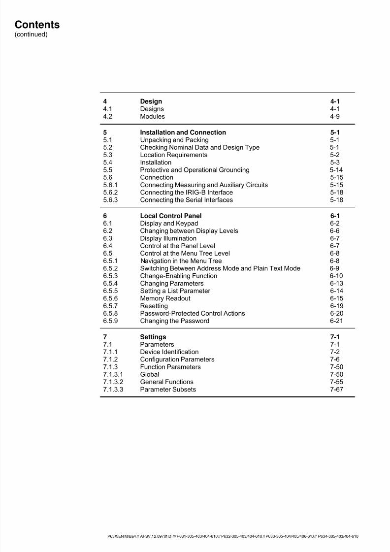
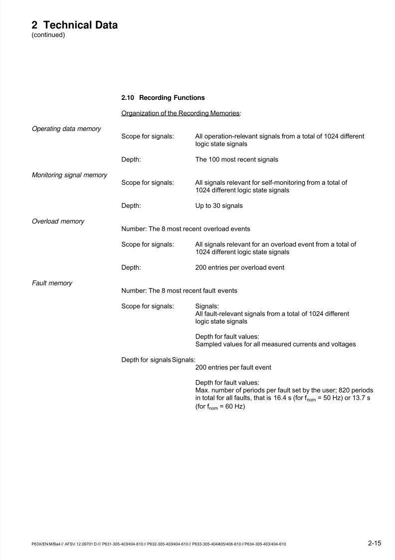
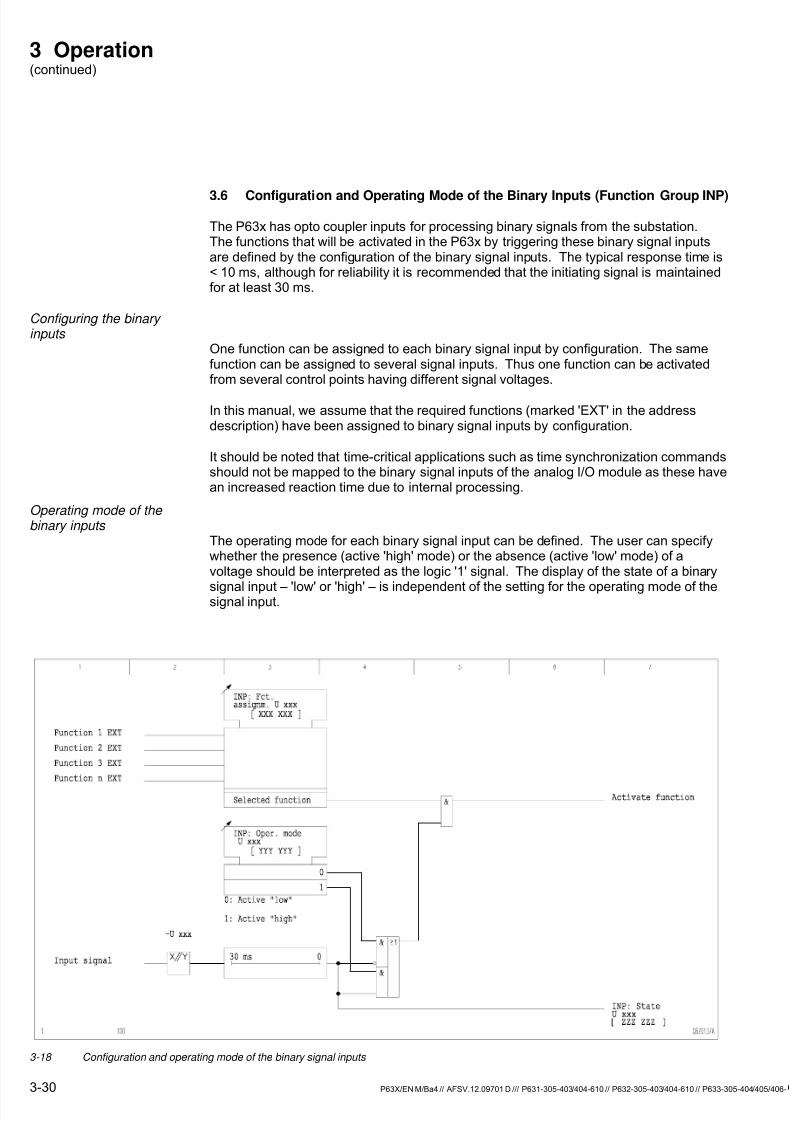
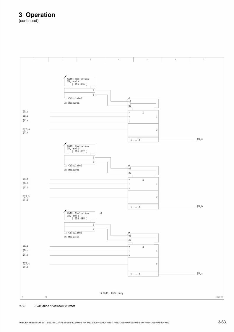
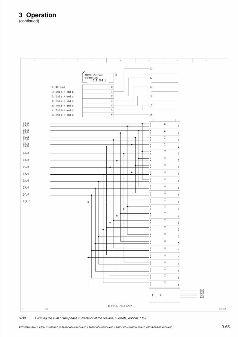
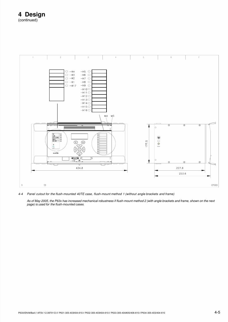
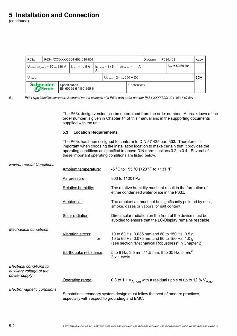
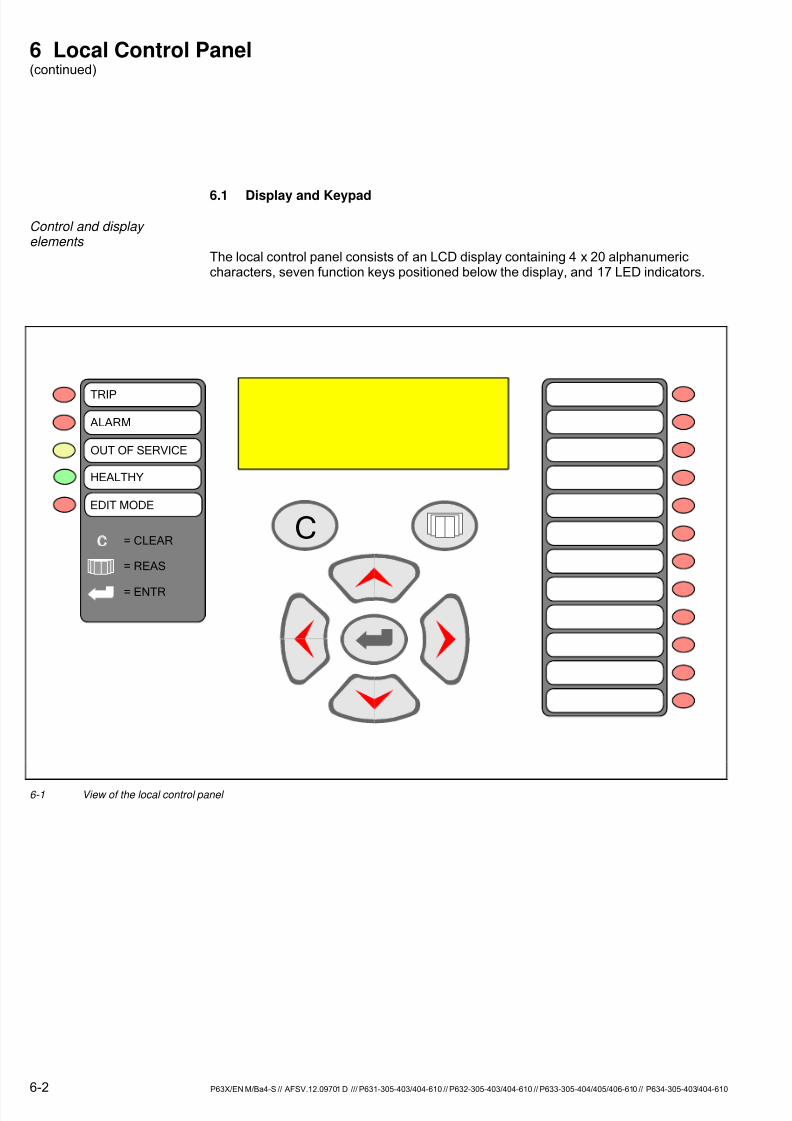
7/11/2019 p63x_en_m_bm6__610-611-620-621__vol_1__

http://slidepdf.com/reader/full/p63xenmbm6610-611-620-621vol1 603/605

7/11/2019 p63x_en_m_bm6__610-611-620-621__vol_1__

http://slidepdf.com/reader/full/p63xenmbm6610-611-620-621vol1 604/605

Schneider Electric

35 rue Joseph Monier 92506 Rueil-Malmaison

FRANCEPhone: +33 (0) 1 41 29 70 00Fax: +33 (0) 1 41 29 71 00

www.schneider-electric.com Publishing: Schneider Electric

Publication: P63x/EN M/Ca4 Version: -610 11/2010

© 2

0 1 0 S

c h n e i d e r E l e c t r i c .

A l l r i g h t s r e s e r v e d .

7/11/2019 p63x_en_m_bm6__610-611-620-621__vol_1__

http://slidepdf.com/reader/full/p63xenmbm6610-611-620-621vol1 605/605


Recommended