PACKAGE POWER DELIVERY ANALYSIS FOR UNMERGED AND MERGED POWER RAILS SEE TAU YEE HUNG A thesis submitted in fulfilment of the requirements for the award of the degree of Master of Engineering (Electrical) Faculty of Electrical Engineering Universiti Teknologi Malaysia DECEMBER 2014
Transcript
PACKAGE POWER DELIVERY ANALYSIS FOR UNMERGED AND MERGED
POWER RAILS
SEE TAU YEE HUNG
A thesis submitted in fulfilment of the
requirements for the award of the degree of
Master of Engineering (Electrical)
Faculty of Electrical Engineering
Universiti Teknologi Malaysia
DECEMBER 2014
iii
To my beloved Wife – Ee San, Daughter -Samantha, Son -Rui Zhe & family members
iv
ACKNOWLEDGEMENT
In the preparation of this thesis, there were many people who provided
resources, advice and various kinds of assistance in making this project successful. I
wish to express my sincere gratitude to my project supervisor, Professor Ir. Dr.
Abdul Halim bin Mohamed Yatim, for not just encouragement but providing lots of
guidance in the form of important theory and giving me focus.
I am also indebted to Intel Microelectronics Sdn. Bhd for funding the tuition
for my pursuit of this Master’s degree. I would also like to thank Universiti
Teknologi Malaysia (UTM) for providing a platform for furthering my studies. I
also give my sincere thanks to all those who provided the background knowledge
needed for this project.
My sincere appreciation also extends to all my colleagues and others who
have provided assistance at various vacations. Their views and tips are useful indeed.
Unfortunately, it is not possible to list all of them in this limited space. I am grateful
to all my family members
v
ABSTRACT
Power delivery design has become important and critical nowadays especially
at the package level, interconnect between silicon and motherboard. It is not an easy
task to perform power delivery analysis at package level as it could have more than
30 power rails and it is very time consuming to validate each of them one by one at a
time. Resonance frequency of power delivery network is critically important to
understand the design risk from power delivery perspective. Inaccuracy of resonance
frequency may result in over design and lead to increase of decoupling solution cost.
This thesis presents a study of modeling extraction for single and multiple power
rails by using Sigrity PowerSI (2.5D field solver) through frequency domain analysis,
focuses on the changes in resonance frequency within each modeling case and
recommends the appropriate way of extracting multiple power rails. The criterion of
modeling extraction methodology in power rails modeling especially for multiple
power rails extraction has been proposed for unmerged power rail and merged power
rail designs. Time domain analysis was carried out to understand the performance of
power delivery network base on the design target and the impact of resonance
frequency of power delivery network. Coupling noise effect has shown significant
impact in merged package design through time domain analysis. The thesis also
reports the comparison of RL network with extracted model for unmerged and
merged power rails design. The generated RL model is correlated with extracted
model in frequency and time domain analysis for unmerged package design. It is
also a good enough model to replace the extracted model of merged package design
by justifying through time domain analysis.
vi
ABSTRAK
Reka bentuk penghantaran kuasa telah menjadi penting dan kritikal pada
masa kini terutamanya di peringkat pakej, sambung antara silikon dan motherboard.
Ia bukan satu tugas yang mudah untuk melaksanakan analisis penghantaran kuasa
pada pakej kerana ia boleh mempunyai lebih daripada 30 landasan kuasa dan ia
adalah sangat memakan masa untuk mengesahkan setiap daripada mereka satu demi
satu setiap masa. Frekuensi resonans rangkaian penghantaran kuasa adalah amat
penting untuk memahami risiko reka bentuk dari perspektif penghantaran kuasa.
Ketidaktepatan frekuensi resonans boleh membawa kepada kesilapan reka bentuk
dan peningkatan kos penyelesaian nyahgandingan. Tesis ini mengemukakan kajian
pemodelan pengekstrakan bagi landasan kuasa tunggal dan berbilang dengan
menggunakan Sigrity PowerSI (2.5D field solver) melalui analisis domain frekuensi,
memberi tumpuan kepada perubahan dalam resonans frekuensi dalam setiap
pemodelan kes dan cara yang sesuai untuk mengeluarkan pelbagai landasan kuasa
yang disyorkan. Kriteria pemodelan pengekstrakan dalam landasan kuasa
pemodelan terutamanya bagi berbilang landasan kuasa pengekstrakan telah
dicadangkan bagi landasan kuasa berasingan dan landasan kuasa bergabung.
Analisis domain masa akan dijalankan untuk memahami prestasi penghantaran kuasa
pangkalan rangkaian, sasaran reka bentuk dan kesan frekuensi resonans rangkaian
penghantaran kuasa. Gandingan kesan bunyi bising telah menunjukkan kesan yang
ketara dalam reka bentuk pakej bergabung melalui analisis domain masa. Tesis juga
melaporkan perbandingan RL rangkaian dengan model yang diekstrak bagi landasan
kuasa berasingan dan bergabung. Tidak ada perbezaan di antara model RL dan
model diekstrak dalam landansan kuasa berasaingan. Ia juga mencukupi untuk
menggantikan model diekstrak dalan landasan kuasa bergabung melalui justifikasi
dalam analisis domain masa.
vii
TABLE OF CONTENTS
CHAPTER TITLE PAGE
DECLARATION ii
DEDICATION iii
ACKNOWLEDGEMENT iv
ABSTRACT v
ABSTRAK vi
TABLE OF CONTENTS vii
LIST OF TABLES ix
LIST OF FIGURES xi
LIST OF ABBREVIATIONS xv
LIST OF SYMBOLS xvi
LIST OF APPENDICES xvii
1 INTRODUCTION 1
1.1 Background of the Problem 1
1.2 Problem Statement 3
1.3 Objectives 5
1.4 Scope of the Study 5
2 LITERATURE REVIEW 7
2.1 Power Delivery Network 7
2.2 Package Design 8
2.3 Power Plane Design 11
2.4 Current Draw/Current Profile 16
2.5 On-die Capacitance 17
viii
2.6 Impedance Profile 17
2.7 Power Delivery Analysis Flow 23
2.8 Power Delivery Analysis Tool 24
2.9 Unmerged Power Rail Design/Analysis 30
2.10 Merged Power Rail Design/Analysis 32
3 RESEARCH METHODOLOGY 35
3.1 Power Delivery Methodology 35
3.2 Power Delivery Network Analysis 41
3.3 Package Power Delivery Modeling 48
4 FREQUENCY DOMAIN ANALYSIS 56
4.1 DC Analysis 56
4.2 Frequency Domain for HSPICE Deck 58
4.3 Solid Power Plane Design Result 59
4.4 Unmerged Package Design Result 62
4.5 Merged Package Design Result 72
4.6 Package Design In Lump Model 77
5 TIME DOMAIN ANALYSIS 89
5.1 Time Domain Analysis Setup 89
5.2 Power rail Current Profile 91
5.3 Solid Power Plane Coupling Noise Result 92
5.4 Unmerge Package Design Result 93
5.5 Merged Package Design Result 106
6 CONCLUSION 112
REFERENCES 115
Appendices A-D 122-129
ix
LIST OF TABLES
TABLE NO. TITLE PAGE
4.1 Target resistance for each power rail 57
4.2 Calculated DC resistance for Power rails A, B and C. 57
4.3 Frequency domain result for single power rail 63
4.4 Impedance and resonance frequency of each power rail 65
4.5 Impedance profile result- resonance frequency 67
4.6 Frequency domain analysis result for Power rail A 69
4.7 Resonance frequency for Power rail B 72
4.8 Resonance frequency for three power rails in merged
package design. 75
4.9 Resonance frequency for dual power rail in merged
package design 76
4.10 Resonance frequency result for Power rails A, B and C 77
4.11 RL model for Power rails A, B and C 79
4.12 Resonance frequency comparison between the Extracted
Model and the RL Model 80
4.13 RL value of different power rails for merged package 82
4.14 Impedance and resonance frequency comparison for
Case 4 86
4.15 Impedance and resonance frequency comparison for
Case 7 87
5.1 Time Domain Analysis Result for single power rail
(Extracted Model) 94
5.2 Time Domain Analysis Result for single power rail in
RL model 96
x
5.3 Noise result for Power A & Power B in dual power
modeling 100
5.4 Noise result for Models 5 and 6 in dual power modeling 101
5.5 Noise result for Power rails A, B and C 105
5.6 Time domain analysis result for merged package design
(Extracted Model) 108
5.7 Time domain analysis result for merged package design
(RL Model) 109
xi
LIST OF FIGURES
FIGURE NO. TITLE PAGE
1.1 Cross section of flip chip package 2
1.2 Common physical components of power delivery network 3
2.1 Equivalent circuit for power delivery network 8
2.2 Cross section of micro via 10
2.3 Plated through hole at package level 10
2.4 Package ball interconnected between the package and
motherboard 11
2.5 Power plane model 13
2.6 Impact of power plane length towards resonance
frequency 14
2.7 Impact of width towards resonance frequency 14
2.8 Resonance frequency change with lower inductance 15
2.9 Resonance frequency changes accordingly with power
plane size. 16
2.10 Series and parallel resonance behaviour 18
2.11 Series resonance 18
2.12 Parallel resonance 19
2.13 Inductance and capacitance behaviour corresponding to
frequency 19
2.14 Equivalent circuit of power delivery network 20
2.15 Series LC network (low frequency) 21
2.16 Parallel LC network (low frequency) 21
2.17 Series LC network (mid frequency) 22
2.18 Parallel LC network (mid frequency) 22
xii
2.19 Plot of impedance profile. 23
2.20 Power Delivery Analysis flow 24
2.21 ANSYS model extraction snapshot 25
2.22 PowerSI tool snapshot 26
2.23 Broadband spice 27
2.24 HSPICE GUI 28
2.25 Cadence Allegro PCB designer. 29
2.26 Equivalent circuit where RL model represents package
power plane, PTHs and balls. 31
2.27 Cross sectional layout representation for unmerged
and merged power plane option 33
2.28 Impedance profile comparison for both split and
merged power planes 34
3.1 Power delivery analysis flow for unmerged and merged
power planes 36
3.2 Flow comparison between RL and extraction modeling 37
3.3 Three power planes design with adjacent ground plane 38
3.4 Single, Dual & Three power plane model 38
3.5 Power planes design with 0.5mm spacing 39
3.6 Power Delivery Network Extraction Flow 40
3.7 PowerSI Modeling Flow 40
3.8 Lumped element model for power delivery. 42
3.9 HSPICE deck for frequency domain analysis 45
3.10 HSPICE deck for time domain analysis 46
3.11 Bump distribution of Power rails A, B and C at the first
layer 49
3.12 Power plane design at third layer (Power rails A, B and
C) 49
3.13 PowerSI Modeling 51
3.14 Port assignment for Power rail A at bump level 52
3.15 Port assignment for Power rail A at package ball 52
3.16 Power rails merged at first layer 53
3.17 Power rails merged at third layer 54
3.18 Power rails merged modeling 55
xiii
4.1 HSPICE deck for frequency domain analysis 58
4.2 Impedance profile for one power plane and three power
plane model 59
4.3 Impedance profile of Power 1 for case 2 and case 3 60
4.4 Impedance profile of Power 1 for various cases 61
4.5 HSPICE setup for Power rails A, B and C in three
HSPICE decks 62
4.6 Impedance profile for Power rails A, B and C 63
4.7 HSPICE setup for dual power rail in three HSPICE decks 64
4.8 Impedance profile for dual power rails modeling
– Model 5 65
4.9 HSPICE setup for three power rails in HSPICE deck 66
4.10 Impedance profile for three power rails modeling 67
4.11 HSPICE deck with only Power rail A 68
4.12 Impedance plots for Power A in Models 1, 3, 4 and 7 69
4.13 Power rail’s bump location at top layer 71
4.14 HSPICE deck setup for merged package design. 73
4.15 Impedance profile for merged package design 74
4.16 Impedance profile in merged package design with
connection of Power rails A and C only 75
4.17 Impedance profile in merged package design with Power
rails A, B and C connected at one time separately. 76
4.18 General schematic diagram of power rail from
unmerged package design. 79
4.19 Comparison between Extracted Model and RL Model
(Power rail A) 80
4.20 General schematic diagram for three main power rails from
merged package layout. 81
4.21 Impedance profile for Extracted Model and RL Model in
merged package design (Case 1) 83
4.22 Comparison between RL model and extracted model for
dual power rails modeling for Case 3 84
4.23 Impedance profile comparison between RL model and
Extracted model (Case 4 – Power rail A) 85
xiv
4.24 Impedance profile comparison between RL model and
Extracted model (Case 4 – Power rail B) 85
4.25 Impedance profile comparison between extracted model
and RL Model (Power rail A) 87
5.1 HSPICE deck for time domain analysis 90
5.2 Top level of time domain analysis in HSPICE 90
5.3 I/O behaviour model (current profile) power rails 91
5.4 Coupling noise of Power 2 with different distance
separation with Power 1 93
5.5 Noise waveforms for Power rails A, B and C in single
power rail modeling 94
5.6 Noise profile comparison between the Extracted Model
& RL Model (Power rail A) 96
5.7 Noise profile comparison between Extracted Model &
RL Model (Power rail B) 97
5.8 HSPICE deck setup for Power rails A and B (Model 4) 98
5.9 Noise waveforms for Power rails A and B in dual power
modeling (Case 1) 99
5.10 Noise waveforms measured at Power rail B, which was
victim of Power rail A 100
5.11 Noise at Power rails B and C in Model 6 (Case 1) 101
5.12 Noise at Power rails B and C in Model 6 (Case 2) 102
5.13 HSPICE setup for Model 7 103
5.14 Noise waveforms for Power rails A, B and C in three
power rails modeling 104
5.15 Self & Coupling noise waveforms for three power rail
modeling (Case 5) 105
5.16 HSPICE deck setup for merged package design. 106
5.17 Noise waveforms for merged package design 107
5.18 Noise waveforms for Case 5 in merged package design 108
5.19 Noise profile comparison between Extracted Model &
RL model (Case 1) 110
5.20 Noise profile comparison between Extracted Model &
RL model (Case 6) 111
xv
LIST OF ABBREVIATIONS
AC - Alternating Current
C4 - Controlled Collapse Chip Connection
DC - Direct Current
EM - Electromagnetic
FEM - Finite Element Method
GND - Ground
IC - Integrated Circuit
ICC - Instantaneous Collector Current
I/O - Input & Output
PCB - Printed Circuit Board
PDN - Power Delivery Network
PKG - Package
PLL - Phase Lock Loop
PTH - Plated Through Hole
PWL - Piece Wise Linear
S-parameter - Scattering parameter
VRM - Voltage Regulator Module
xvi
LIST OF SYMBOLS
A - Ampere
C - Capacitance
D - Dimension
e.g. - example
F - Farad
G - Giga
Hz - Hertz
H - Henry
k - kilo
L - Inductance
M - Mega
m - mille
n - nano
R - Resistance
V - Volt
w - Omega
Z - Impedance
µ - micro
Ω - Ohm
xvii
LIST OF APPENDICES
APPENDIX TITLE PAGE
A Frequency domain deck in HSPICE 122
B Time domain deck in HSPICE 123
C Equivalent R and L Calculation 124
D Power Delivery Modeling 125
CHAPTER 1
INTRODUCTION
1.1 Background of the Problem
Cost-effective power delivery design has become an important determinant
influencing designs nowadays, which can be achieved through comprehensive power
delivery design. Power delivery design has becomes critical and important in silicon,
package and board application [1]. The market nowadays opt for novel power
delivery design which are affordable and competitive in cost, which is a major
challenge faced by the silicon and packaging industry. Designing a cost effective
and optimized power delivery design at package level is no easy task [9].
The primary function of package is to provide mechanical support and
electrical interconnects between silicon and motherboard. It acts as an interconnect
for transmitting I/O signals from the silicon to the motherboard and it also supplies
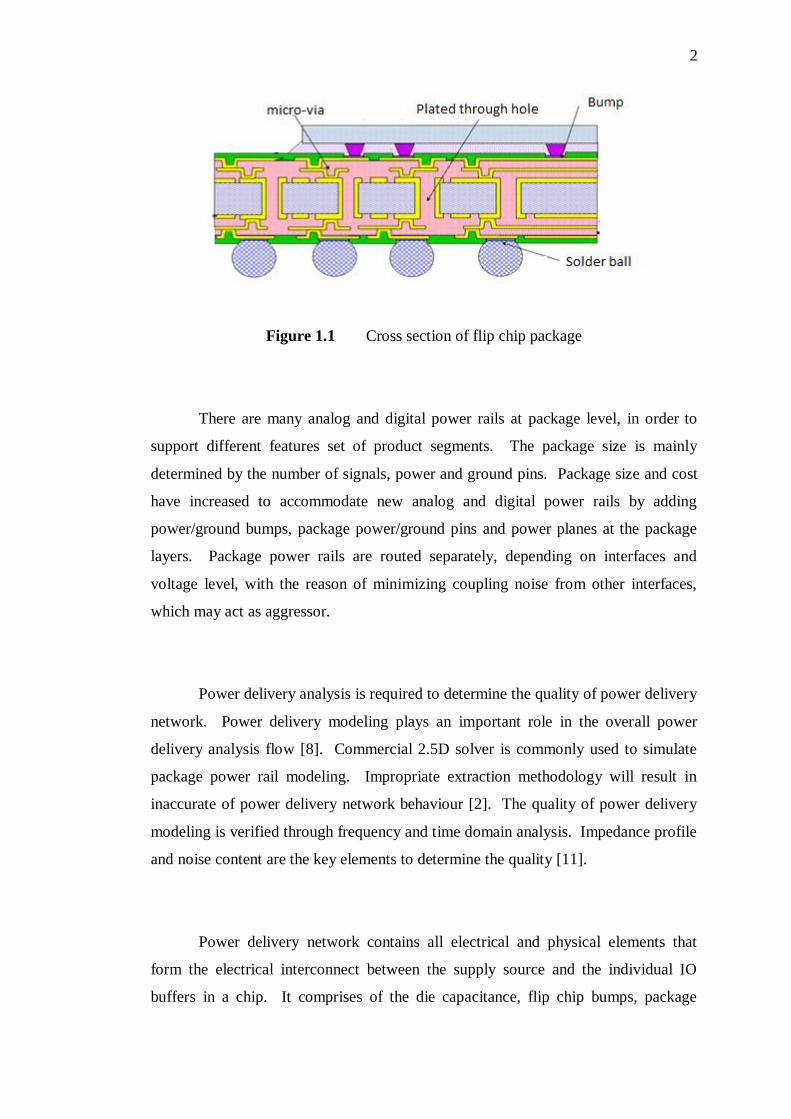
clean power and reference voltage to the active devices on the die. Figure 1.1 shows
the cross section of a flip chip package which consists of bump, micro-via, plated
through holes (PTH) and solder ball.
2
Figure 1.1 Cross section of flip chip package
There are many analog and digital power rails at package level, in order to
support different features set of product segments. The package size is mainly
determined by the number of signals, power and ground pins. Package size and cost
have increased to accommodate new analog and digital power rails by adding
power/ground bumps, package power/ground pins and power planes at the package
layers. Package power rails are routed separately, depending on interfaces and
voltage level, with the reason of minimizing coupling noise from other interfaces,
which may act as aggressor.
Power delivery analysis is required to determine the quality of power delivery
network. Power delivery modeling plays an important role in the overall power
delivery analysis flow [8]. Commercial 2.5D solver is commonly used to simulate
package power rail modeling. Impropriate extraction methodology will result in
inaccurate of power delivery network behaviour [2]. The quality of power delivery
modeling is verified through frequency and time domain analysis. Impedance profile
and noise content are the key elements to determine the quality [11].
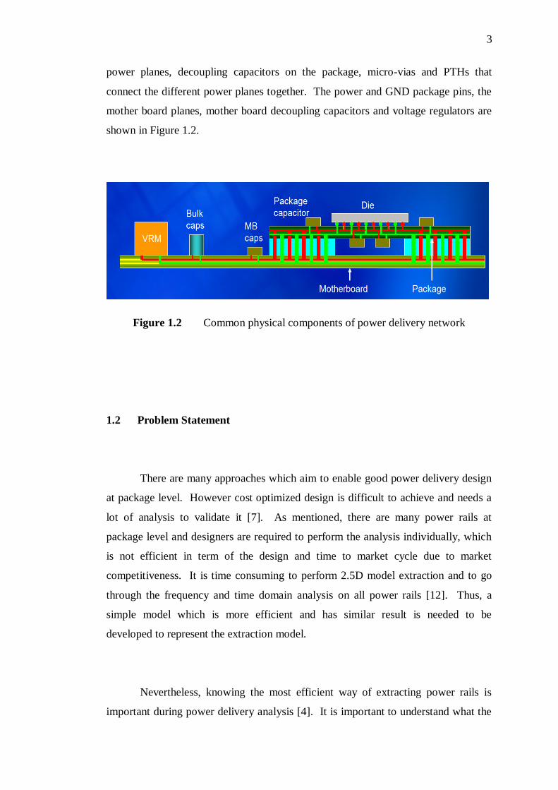
Power delivery network contains all electrical and physical elements that
form the electrical interconnect between the supply source and the individual IO
buffers in a chip. It comprises of the die capacitance, flip chip bumps, package
3
power planes, decoupling capacitors on the package, micro-vias and PTHs that
connect the different power planes together. The power and GND package pins, the
mother board planes, mother board decoupling capacitors and voltage regulators are
shown in Figure 1.2.
Figure 1.2 Common physical components of power delivery network
1.2 Problem Statement
There are many approaches which aim to enable good power delivery design
at package level. However cost optimized design is difficult to achieve and needs a
lot of analysis to validate it [7]. As mentioned, there are many power rails at
package level and designers are required to perform the analysis individually, which
is not efficient in term of the design and time to market cycle due to market
competitiveness. It is time consuming to perform 2.5D model extraction and to go
through the frequency and time domain analysis on all power rails [12]. Thus, a
simple model which is more efficient and has similar result is needed to be
developed to represent the extraction model.
Nevertheless, knowing the most efficient way of extracting power rails is
important during power delivery analysis [4]. It is important to understand what the
4
required criteria are, while extracting power rails from package design. Neglecting
these criteria will cause inaccuracy in frequency and time domain analysis. Thus,
any optimization design based on this power delivery model may not be valid. To
date, there is no proper guide for extracting single or multiple power rails in single
model [10]. Behaviour change in impedance profile is unknown if multiple power
rails are extracted as a single model, which may create risk to the power delivery
performance. Nevertheless, there are many merged power rail designs nowadays [1].
Coupling effect, behaviour change in frequency and time domain are not straight
forward as compared to single and isolated design power rail [6].
Modern electronic devices such as tablets and smartphones are getting more
powerful and efficient. The demand in feature sets, functionality and usability
increase exponentially and this has posed a greater challenge to the design of a power
distribution network (PDN). Power rails merging is a popular option adopted today
in a PDN design as the provision of numerous power rails is no longer feasible due to
form factor limitation and cost constraint [39]. High performance smartphones and
tablets products cycle has been shorten from one year cadence to six months or even
three months cadence. It also leads the new product cycle especially derivative
product cycle is even shorter although comes with less feature and lower cost. In
order to deliver product in short cycle to gain more market share, cost effective
power delivery solution where power rail merging is one of it. Nevertheless, due to
short schedule an efficient analysis method is required to analyze power rail merging.
The purpose of merging power rails at package level includes
Improving the package design efficiency by reducing the number of
power rails
Enabling smaller packages and lower number of package layers
through lesser micro-via, PTH and package ball for cost saving
opportunity
Potential decoupling sharing at silicon, package and board levels for
cost saving.
Reducing possibility on adding extra voltage regulator at board level.
5
There are many benefits of merging power rail design; undeniably, but more
challenges are expected more as compared to single power rail design. There are
risks of violating the noise target and introducing bad coupling noise to sensitive
power rails.
1.3 Objectives
The objectives of this project are to determine the selection criteria of power
delivery modeling for both unmerged and merged power rails design at package level,
and propose an efficient method for performing power delivery analysis for single
and multiple power rails through RL model. In this study, the RL model was verified
through frequency and time domain analysis and was correlated with the extracted
model. The proposed method is hoped able to help create awareness and serve as a
reference guideline to the power delivery community in power delivery modeling at
package level, especially for merged power rails design.
1.4 Scope of the Study
The project scope included the understanding on the current power delivery
methodology at package level. It involved the background of package design as
well. Two different package power rail designs were designed, which were
unmerged and merged power rail design.
There were three major stages in this project, starting with package power rail
design, followed by modeling/extraction, and then performing the frequency and
6
time domain analysis based on the models that has been created. An improved
modeling methodology was also established which would be used to determine the
criterion of modeling for both single and multiple power rails. RL model was also
generated for comparison with the extracted model for both unmerged and merged
power rail design. Nevertheless, three commercial software were needed in this
thesis, for example: Sigrity PowerSI 2.5D solver is used to extract power rail model,
Allegro is used to design power rails layout and HSPICE is used to perform
frequency and time domain analysis.
Literature review is discussed in Chapter 2, which discusses the general
overview of power delivery network, impedance profile, existing power delivery
flow and tools that were used in the power delivery analysis. Chapter 3 discusses the
power delivery analysis flow that includes frequency and time domain analysis. This
chapter also covers the power delivery modeling cases. Chapters 4 and 5 discuss the
results of the frequency and time domain analysis, which contained the impedance
profile and noise content, compared between the extracted and RL model. The
frequency domain contained the resonance frequency, which is a critical element in
power delivery analysis. The findings from this study deliver the importance of the
selection criteria that determine the accuracy of the resonance frequency during
power delivery modeling; neglecting it will result in inaccuracy of resonance
frequency. Time domain analysis was also performed to verify if the proposed RL
model is sufficient to represent the extracted model. Finally, Chapter 6 presents the
conclusion of this study.
115
REFERENCE
1. Suarez-Gartner, R.E. (1998). System technology challenges facing the PC
industry. Proceeding of the 1998 International Conference on Distributed
Computing Systems. 2-3 Feb. Santa Cruz, CA: IEEE. 2-3.
2. Radhakrishnan, K.; Li, Y.-L. and Pinello, W.P.(2001). Integrated modeling
methodology for core and I/O power delivery. Proceeding of the 2001
Electronic Components and Technology Conference. 29 May-01 Jun. Orlando,
FL: IEEE. 1107-1110.
3. Weimin Shi and Wright, C. (2001). A novel efficient approach of including
frequency-dependent power delivery effects in bus signal integrity simulation.
Proceeding of the 2001 Electrical Performance of Electronic Packaging and
Systems. 29-31 Oct. Cambridge, MA: IEEE. 303-306.
4. Quan Qi; Quint, D.; and Michalka, T.(2002). Simulation of a coupled signal
and power delivery system in an electronics package. Proceeding of the 2002
IEEE Electronic Components and Technology. San Diego, California: IEEE.
311-318.
5. Zhong Chen and Lewis, D.(2005). Evaluating uncertainties in net power
delivery using dual directional couplers. International Symposium of the 2005
Electromagnetic Compatibility. 8-12 Aug. Chicago, IL: IEEE. 782-786
116
6. Rangaswamy,G.K.and Prathaban, S(2006). Signal Integrity Analysis with
Power Delivery Network. Workshop of the 2006 IEEE Signal And Power