Packaging and Fab of Electronics for Harsh Environments (Continuation of an FY08 Task) Description: FY09 Plans: Costs: Lead Center/PI: MSFC/Melanie Bodiford Center Funding Split: NASA and Non-NASA Organizations/Procurements Deliverables: •CAVE review status reports •Report on flexible Interconnects •Report on solder alloys for low-temp applications •Updated modeling tools •Lessons learned from implementation of flexible interconnects – compare/contrast available interconnects •Participate in the semi-annual project reviews and serve as the primary NASA member of the advisory boards to CAVE. •Evaluate reliability of solder alloys for low-temp applications •Provide status reports on CAVE progress. •Evaluate flexible interconnects for ceramic area array parts •Evaluate ceramic interconnects when exposed to combined environments •Participate in conferences/symposiums to gather data •Evaluation of new/emerging technologies for packaging and fabrication of electronics for harsh environments. •Provide research consortium membership (Auburn CAVE) •Provide updated modeling tools for NASA parts selection •Provide updated reliability test database for use in NASA parts selection •Low-temp solder tests (fixtures/samples) (MSFC/Auburn procurement) •Test vehicles (flexible interconnects) procurement) •Jacobs-Sverdrup
Transcript
Packaging and Fab of Electronics for Harsh Environments (Continuation of an FY08 Task)
Description: FY09 Plans:
Costs:
Lead Center/PI: MSFC/Melanie Bodiford
Center Funding Split:
NASA and Non-NASA Organizations/Procurements:
Deliverables:•CAVE review status reports•Report on flexible Interconnects•Report on solder alloys for low-temp applications•Updated modeling tools•Lessons learned from implementation of flexible interconnects – compare/contrast available interconnects
•Participate in the semi-annual project reviews and serve as the primary NASA member of the advisory boards to CAVE.
•Evaluate reliability of solder alloys for low-temp applications
•Provide status reports on CAVE progress.
•Evaluate flexible interconnects for ceramic area array parts
•Evaluate ceramic interconnects when exposed to combined environments
•Participate in conferences/symposiums to gather data
•Evaluation of new/emerging technologies for packaging and fabrication of electronics for harsh environments.
•Provide research consortium membership (Auburn CAVE)
•Provide updated modeling tools for NASA parts selection
•Provide updated reliability test database for use in NASA parts selection
Packaging and Fab of Electronics for Harsh Environments (Continuation of an FY08 Task)
Flexible Interconnects for Ceramic Grid Arrays – explore interconnects to provide better thermal expansion matching between ceramic and epoxy glass and enable easier assembly
.020” X .050” BeCu fuzz button on Sn63 solder bumps
BeCu Microspring (.020”X.050” SnPb
plated)
In W
ork
Pb95/Sn5 column (wire & injection
molded)
Packaging and Fab of Electronics for Harsh Environments (Continuation of an FY08 Task)
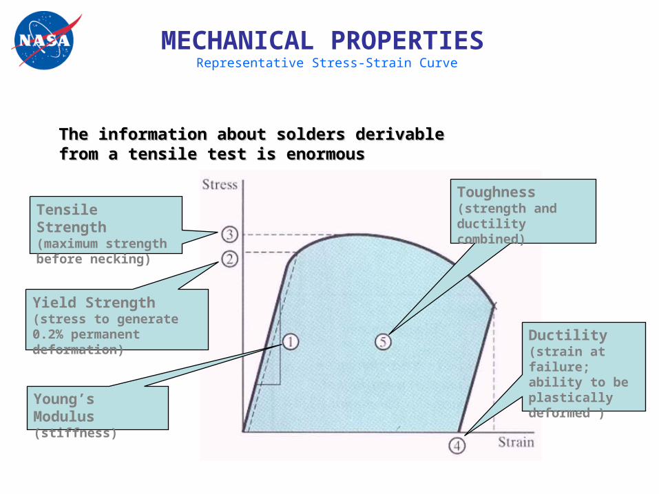
Extreme Low Temperature Behavior of SoldersEvaluate mechanical behavior, mechanical properties, and microstructure changes of solder alloys exposed to extreme low temperatures (-190 C to -270 C)
• Motivation: Sensors and feed-through connectors on Constellation/Areas and Shuttle missions are exposed to extreme low temperatures. Mechanical property data for solders at cryogenic temperatures doesn’t exist, and is needed for design and qualification
• Approach: Measure stress-strain and creep behavior of small cast solder tensile samples using the low temperature capable mechanical testing setup at Auburn University/CAVE
• Low temperature behavior of solders using existing testing machine and chamber (-190 C, cooled by cold gas from LN2 )
• Room temperature behavior and microstructure of solders after exposures to extreme low temperature thermal shocks such as obtained by immersion in LN2 (-196 C) and LHe (-269 C)
• Effects of extreme low temperature thermal cycling on solder behavior and microstructure
• Begin development of test system with vacuum chamber for in-situ testing at extreme low temperatures (-190 C to -270 C)