Page 1
Electronic Components and Technology Conference
Packaging Challenges and Solutions for Silicon Carbide Power Electronics
Ljubisa Stevanovic, Ph.D. Chief Engineer and Advanced Technology Leader, GE Global Research, Niskayuna, NY [email protected] Presented at: ECTC Panel Session: Power Electronics – A Booming Market, San Diego, 29 May, 2012
Page 2
L. Stevanovic, Power Electronics – A Booming Market, 2
Semiconductor Materials for Power Electronic Devices
Page 3
L. Stevanovic, Power Electronics – A Booming Market, 3
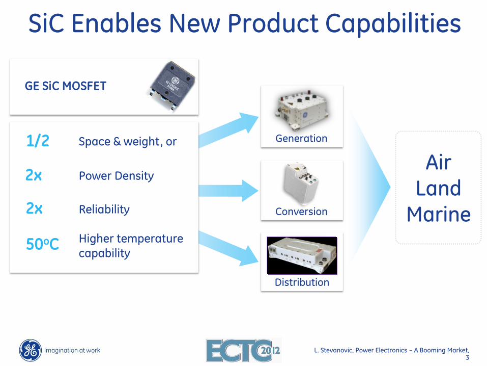
SiC Enables New Product Capabilities
GE SiC MOSFET
1/2 Space & weight, or
2x
50oC
Reliability
Higher temperature capability
Generation
Conversion
Distribution
Power Density 2x Air
Land Marine
Page 4
L. Stevanovic, Power Electronics – A Booming Market, 4
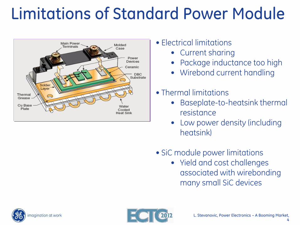
Limitations of Standard Power Module
• Electrical limitations • Current sharing • Package inductance too high • Wirebond current handling
• Thermal limitations • Baseplate-to-heatsink thermal
resistance • Low power density (including
heatsink)
• SiC module power limitations • Yield and cost challenges
associated with wirebonding many small SiC devices
Page 5
L. Stevanovic, Power Electronics – A Booming Market, 5
• Minimize voltage overshoot / derating
• Reduce switching losses, or increase frequency
• Minimize snubber requirements
OFF
loopst
ILV
Importance of Low Inductance
Page 6
L. Stevanovic, Power Electronics – A Booming Market, 6
Adhesive
Die Die
Polyimide Copper
Die Metallization
<200 µm GE POL Structure
Die Die Die Metallization
Aluminum wirebond
>2000 µm
Wirebond Structure
Low & matched parasitics - Low Inductance, Low Resistance; High current capability : Power Efficiency
Reducing size and weight while maintaining performance: System Cost
Eliminate wire-bonds and solder-bumps: Power Efficiency & Performance
Ability to array multiple die: System Cost
2
3
4
1
1
2
3
4
Power OverLay (POL) Interconnect PWB-like planar interconnect for power packaging
Page 7
L. Stevanovic, Power Electronics – A Booming Market, 7
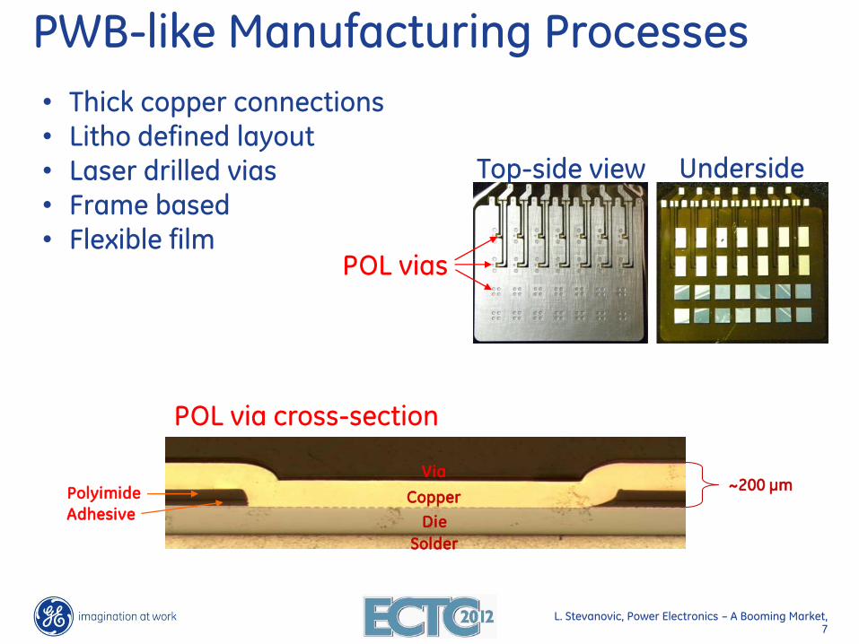
• Thick copper connections • Litho defined layout • Laser drilled vias • Frame based • Flexible film
~200 µm
Top-side view Underside
Copper
Die
Solder
Polyimide
Adhesive
Via
POL via cross-section
PWB-like Manufacturing Processes
POL vias
Page 8
L. Stevanovic, Power Electronics – A Booming Market, 8
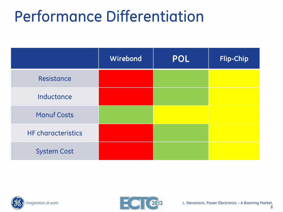
Performance Differentiation
Wirebond POL Flip-Chip
Resistance
Inductance
Manuf Costs
HF characteristics
System Cost
Page 9
L. Stevanovic, Power Electronics – A Booming Market, 9
SiC Power Module –Switching Test 11ns inductive switching at: VDS = 540V, ID = 300A
Page 10
L. Stevanovic, Power Electronics – A Booming Market, 10
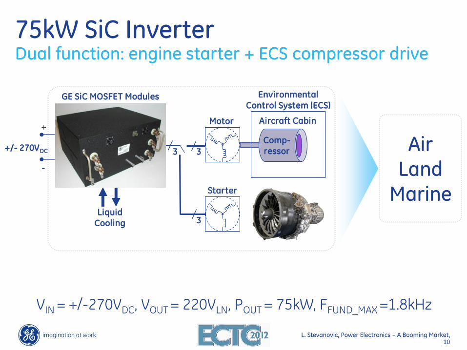
VIN = +/-270VDC, VOUT = 220VLN, POUT = 75kW, FFUND_MAX =1.8kHz
Motor
Comp-ressor +/- 270VDC
+
-
3
Liquid Cooling
Aircraft Cabin
Environmental Control System (ECS)
3
3
Starter
GE SiC MOSFET Modules
75kW SiC Inverter Dual function: engine starter + ECS compressor drive
Air Land
Marine
Page 11
L. Stevanovic, Power Electronics – A Booming Market, 11
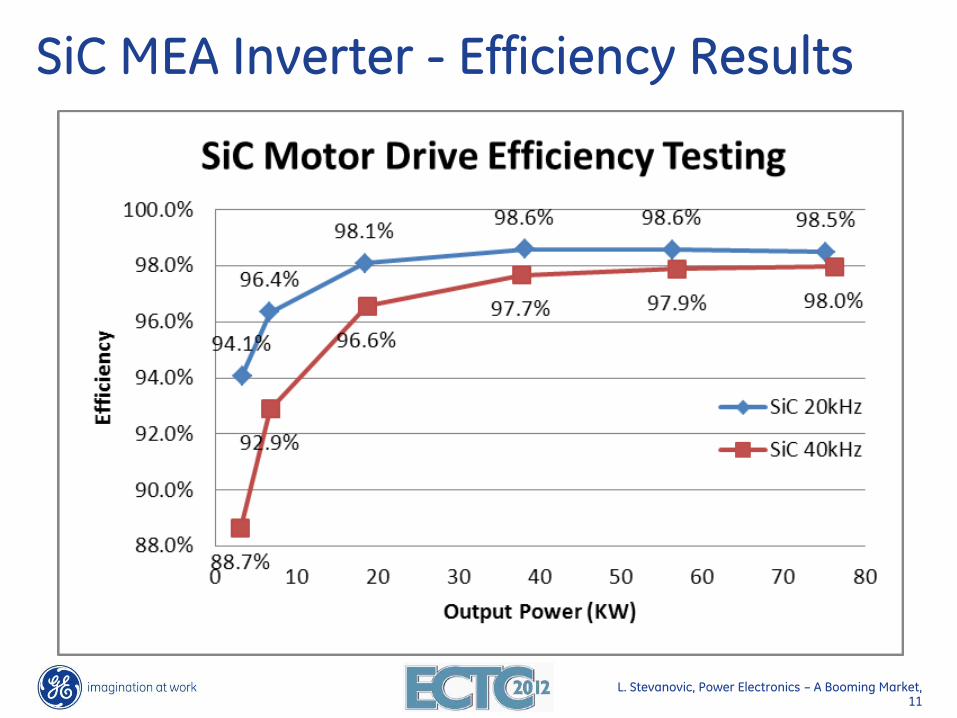
SiC MEA Inverter - Efficiency Results
Page 12
L. Stevanovic, Power Electronics – A Booming Market, 12
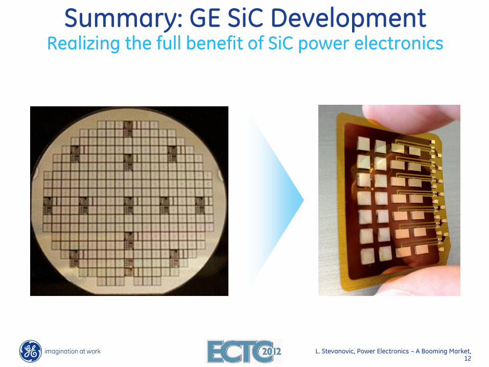
Summary: GE SiC Development Realizing the full benefit of SiC power electronics