Packaging trends for advanced Cmos
technology nodes
Michel Garnier
Packaging & Test Manufacturing
Corporate Packaging & Automation
STMicroelectronics
Advanced Packaging Session, Semicon Russia
6th June 2013
Content
• STMicroelectronics presentation • General presentation
• R&D Packaging @ STM
• Packaging Platforms covered at ST
• Packaging development for Advanced Cmos technologies • Business segments
• Main requests
• Cu pillar for FC packages
• Cu RDL for WLPs…
• Conclusions
2
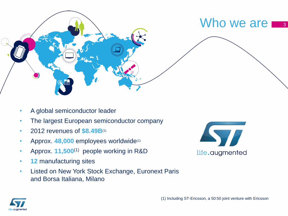
• A global semiconductor leader
• The largest European semiconductor company
• 2012 revenues of $8.49B(1)
• Approx. 48,000 employees worldwide(1)
• Approx. 11,500(1) people working in R&D
• 12 manufacturing sites
• Listed on New York Stock Exchange, Euronext Paris
and Borsa Italiana, Milano
Who we are 3
(1) Including ST-Ericsson, a 50:50 joint venture with Ericsson
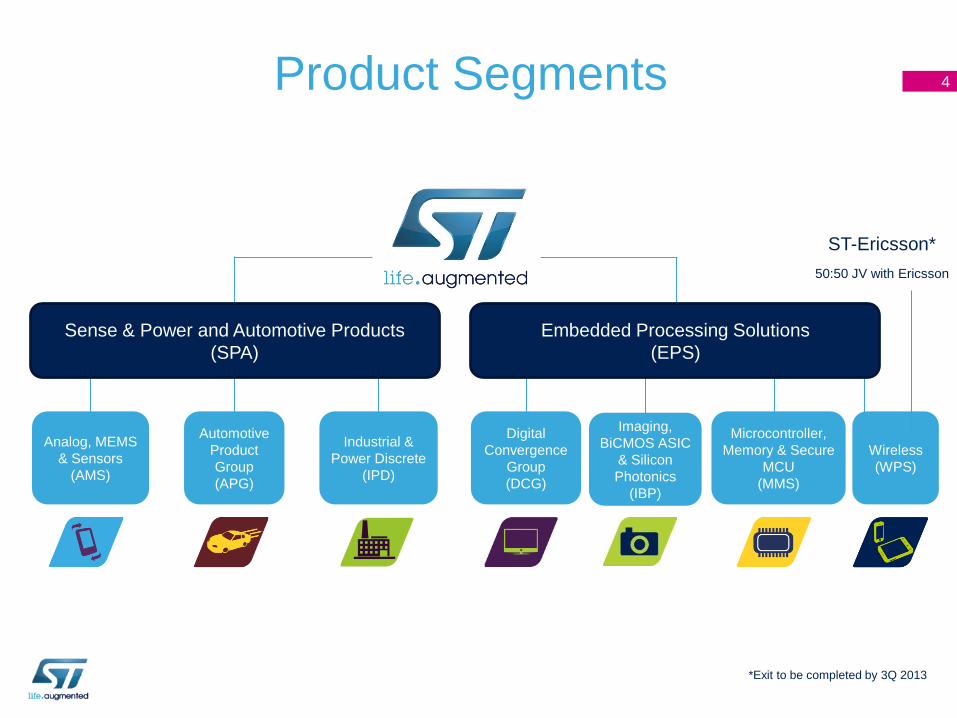
Product Segments 4
Digital
Convergence
Group
(DCG)
Imaging,
BiCMOS ASIC
& Silicon
Photonics
(IBP)
Automotive
Product
Group
(APG)
Analog, MEMS
& Sensors
(AMS)
Microcontroller,
Memory & Secure
MCU
(MMS)
Embedded Processing Solutions
(EPS)
Industrial &
Power Discrete
(IPD)
Sense & Power and Automotive Products
(SPA)
Wireless
(WPS)
*Exit to be completed by 3Q 2013
ST-Ericsson*
50:50 JV with Ericsson
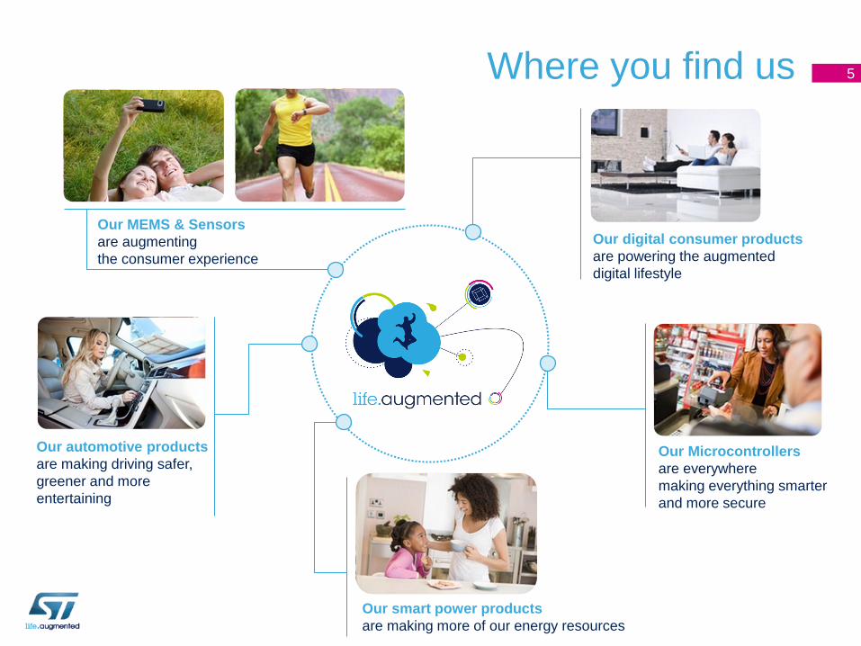
Where you find us 5
Our automotive products
are making driving safer,
greener and more
entertaining
Our smart power products
are making more of our energy resources
Our MEMS & Sensors
are augmenting
the consumer experience
Our Microcontrollers
are everywhere
making everything smarter
and more secure
Our digital consumer products
are powering the augmented
digital lifestyle
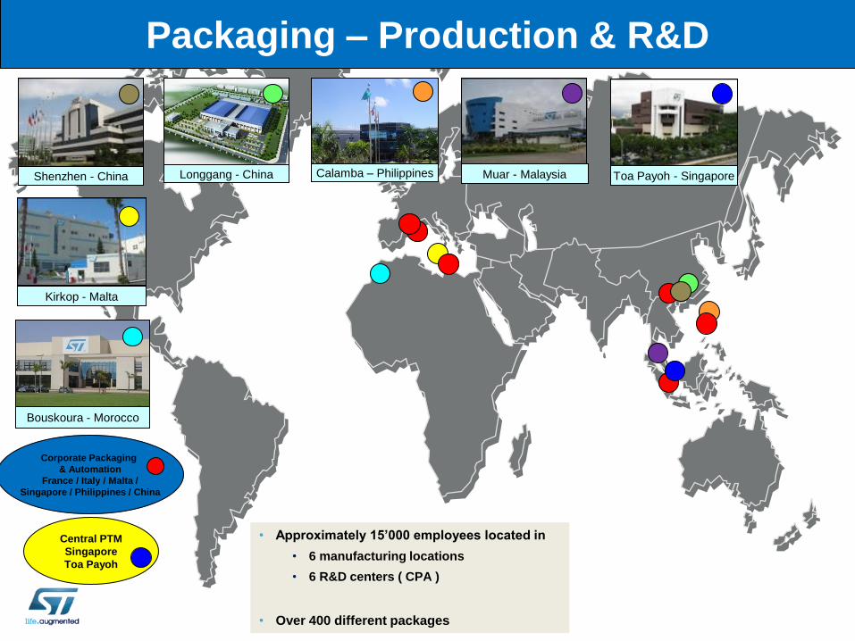
Bouskoura - Morocco
Calamba – Philippines Longgang - China Shenzhen - China
Kirkop - Malta
Muar - Malaysia
Central PTM
Singapore
Toa Payoh
Toa Payoh - Singapore
Corporate Packaging
& Automation
France / Italy / Malta /
Singapore / Philippines / China
Packaging – Production & R&D
• Approximately 15’000 employees located in
• 6 manufacturing locations
• 6 R&D centers ( CPA )
• Over 400 different packages
7
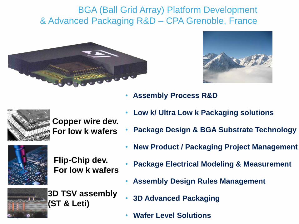
BGA (Ball Grid Array) Platform Development
& Advanced Packaging R&D – CPA Grenoble, France
• Assembly Process R&D
• Low k/ Ultra Low k Packaging solutions
• Package Design & BGA Substrate Technology
• New Product / Packaging Project Management
• Package Electrical Modeling & Measurement
• Assembly Design Rules Management
• 3D Advanced Packaging
• Wafer Level Solutions
Copper wire dev.
For low k wafers
3D TSV assembly
(ST & Leti)
Flip-Chip dev.
For low k wafers
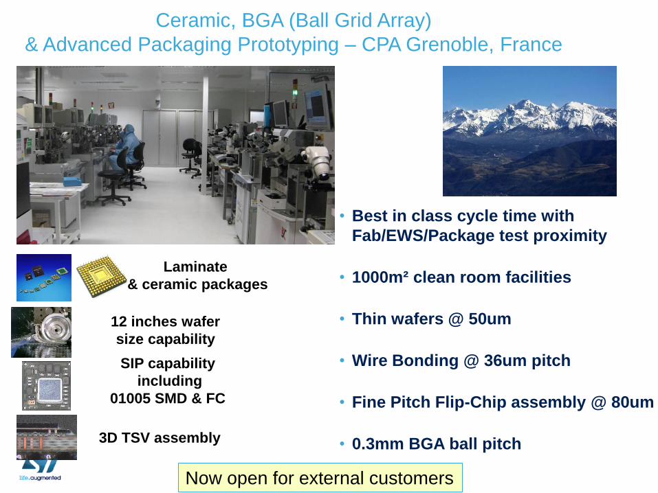
Ceramic, BGA (Ball Grid Array)
& Advanced Packaging Prototyping – CPA Grenoble, France
• Best in class cycle time with
Fab/EWS/Package test proximity
• 1000m² clean room facilities
• Thin wafers @ 50um
• Wire Bonding @ 36um pitch
• Fine Pitch Flip-Chip assembly @ 80um
• 0.3mm BGA ball pitch
Laminate
& ceramic packages
12 inches wafer
size capability
SIP capability
including
01005 SMD & FC
3D TSV assembly
Now open for external customers
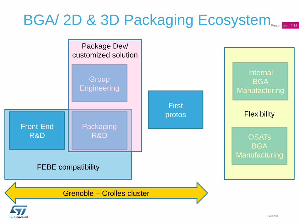
FEBE compatibility
BGA/ 2D & 3D Packaging Ecosystem 9
6/6/2013
Presentation Title
Front-End
R&D
Packaging
R&D
Group
Engineering
Internal
BGA
Manufacturing
OSATs
BGA
Manufacturing
Package Dev/
customized solution
Flexibility First
protos
Grenoble – Crolles cluster
Content
• STMicroelectronics presentation • General presentation
• R&D Packaging @ STM
• Packaging Platforms covered at ST
• Packaging development for Advanced Cmos technologies • Business segments
• Main requests
• Cu pillar for FC packages
• Cu RDL for WLPs…
• Conclusions
10
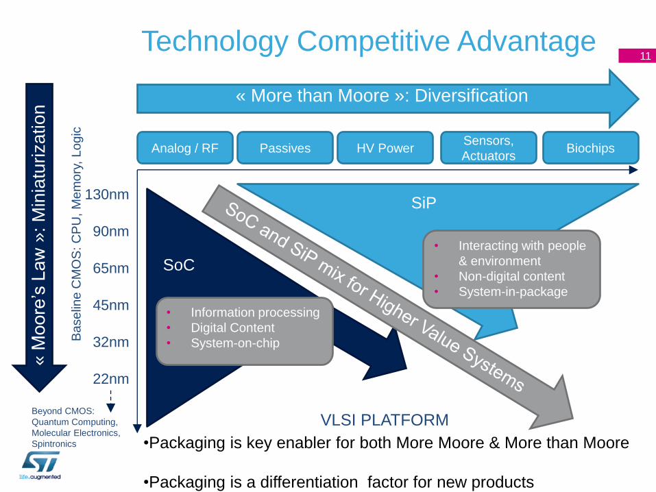
Technology Competitive Advantage
Beyond CMOS:
Quantum Computing,
Molecular Electronics,
Spintronics
« More than Moore »: Diversification
« M
oo
re’s
La
w »
: M
inia
turiza
tio
n
Analog / RF Passives HV Power Sensors,
Actuators Biochips
130nm
90nm
65nm
45nm
32nm
22nm
Ba
se
line
CM
OS
: C
PU
, M
em
ory
, Logic
SoC
SiP
VLSI PLATFORM
• Information processing
• Digital Content
• System-on-chip
• Interacting with people
& environment
• Non-digital content
• System-in-package
11
•Packaging is key enabler for both More Moore & More than Moore
•Packaging is a differentiation factor for new products
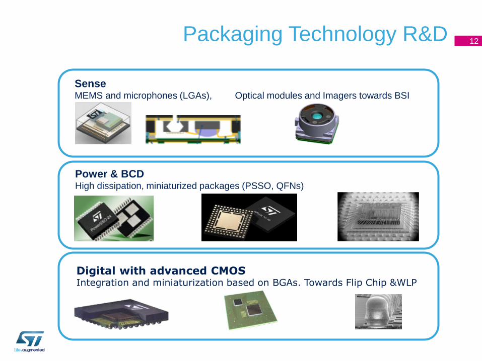
Packaging Technology R&D 12
Sense MEMS and microphones (LGAs), Optical modules and Imagers towards BSI
Power & BCD High dissipation, miniaturized packages (PSSO, QFNs)
Digital with advanced CMOS Integration and miniaturization based on BGAs. Towards Flip Chip &WLP
13
Packaging technology roadmap
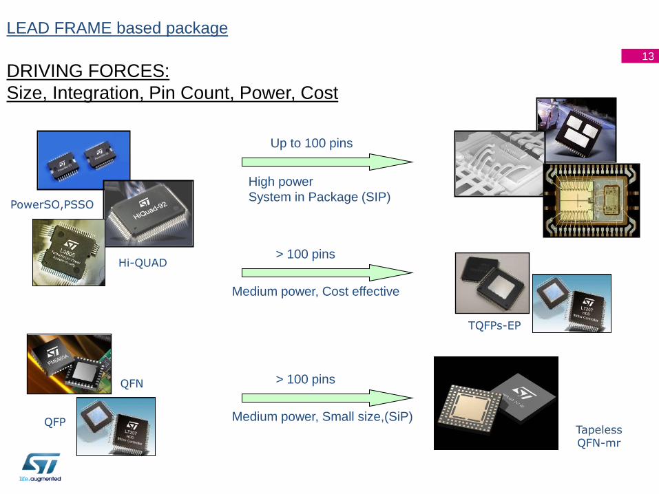
LEAD FRAME based package
DRIVING FORCES:
Size, Integration, Pin Count, Power, Cost
Hi-QUAD
High power
System in Package (SIP)
Up to 100 pins
Medium power, Cost effective
> 100 pins
PowerSO,PSSO
TQFPs-EP
Medium power, Small size,(SiP)
> 100 pins QFN
QFP
Tapeless QFN-mr
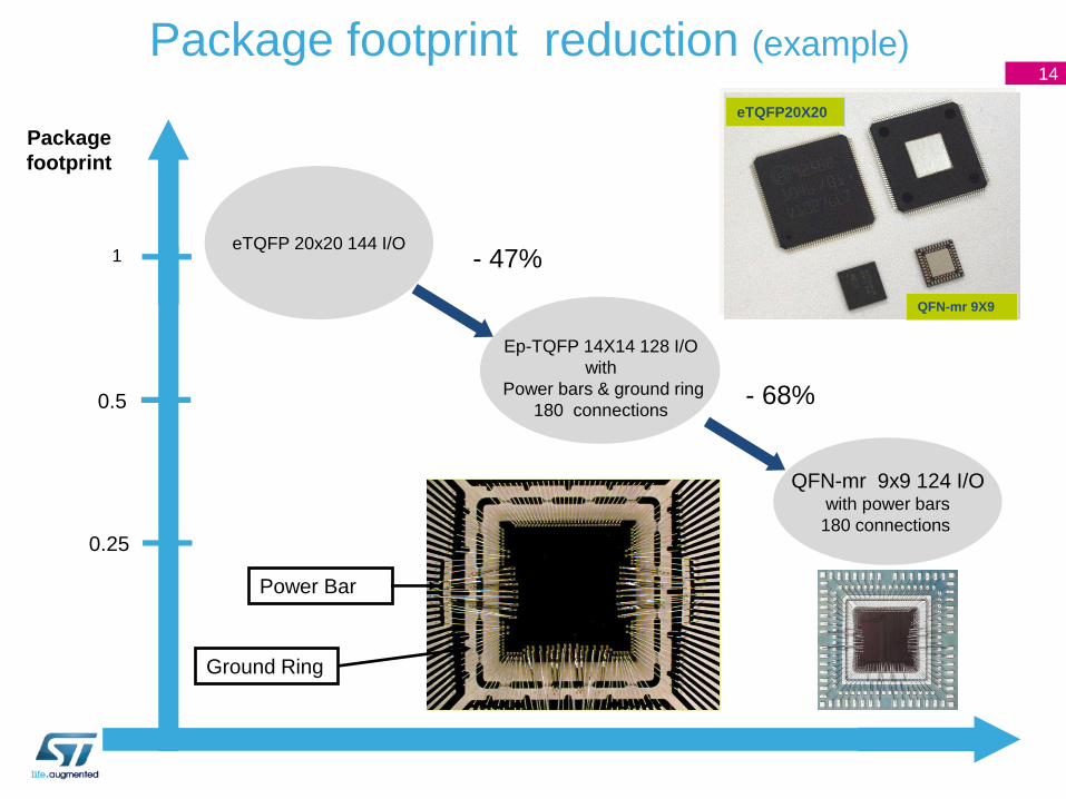
Package footprint reduction (example)
eTQFP 20x20 144 I/O
QFN-mr 9x9 124 I/O with power bars
180 connections
Package
footprint
0.5
1
0.25
eTQ 20X20
eTQFP20X20
QFN-mr 9X9
- 47%
- 68%
Ep-TQFP 14X14 128 I/O
with
Power bars & ground ring
180 connections
Power Bar
Ground Ring
14
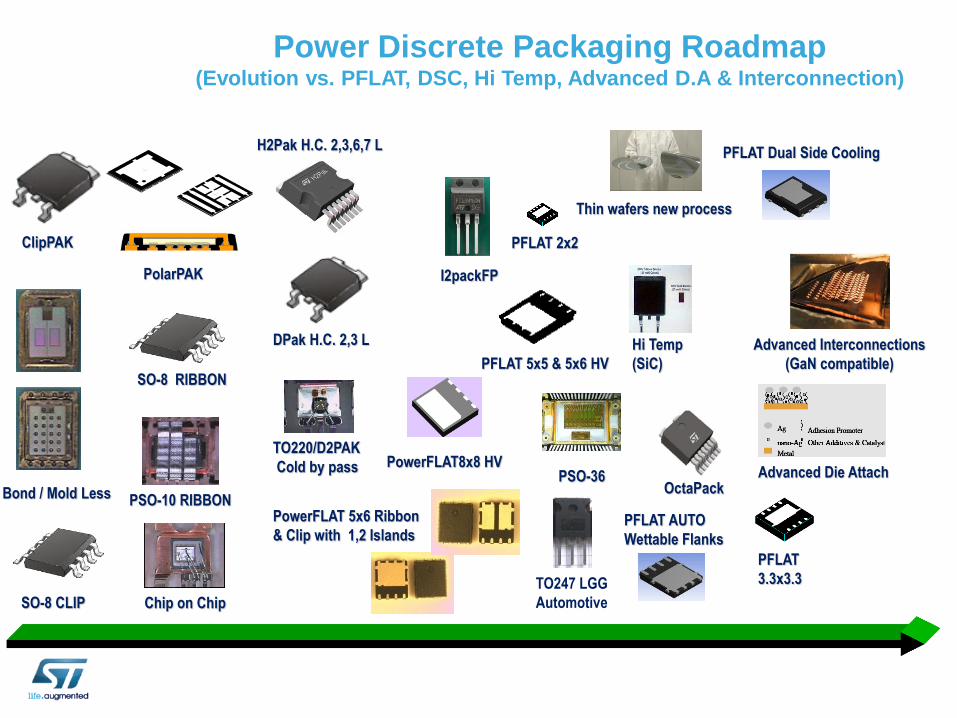
ClipPAK
SO-8 CLIP
Power Discrete Packaging Roadmap (Evolution vs. PFLAT, DSC, Hi Temp, Advanced D.A & Interconnection)
SO-8 RIBBON
DPak H.C. 2,3 L
H2Pak H.C. 2,3,6,7 L
PolarPAK
PowerFLAT8x8 HV
PFLAT Dual Side Cooling
PowerFLAT 5x6 Ribbon
& Clip with 1,2 Islands
PFLAT
3.3x3.3
PFLAT 5x5 & 5x6 HV
Bond / Mold Less
TO247 LGG
Automotive
OctaPack
Chip on Chip
I2packFP
Hi Temp
(SiC)
PFLAT 2x2
PSO-10 RIBBON
PSO-36
TO220/D2PAK
Cold by pass Advanced Die Attach
Thin wafers new process
PFLAT AUTO
Wettable Flanks
Advanced Interconnections
(GaN compatible)
16
06/06/2013 Presentation Title
Content
• STMicroelectronics presentation • General presentation
• R&D Packaging @ STM
• Packaging Platforms covered at ST
• Packaging development for Advanced Cmos technologies • Business segments
• Main requests
• Cu pillar for FC packages
• Cu RDL for WLPs…
• Conclusions
17
Packaging Technology R&D 18
Sense MEMS and microphones (LGAs), Optical modules and Imagers towards BSI
Power & BCD High dissipation, miniaturized packages (PSSO, QFNs)
Digital with advanced CMOS Integration and miniaturization based on BGAs. Towards Flip Chip &WLP
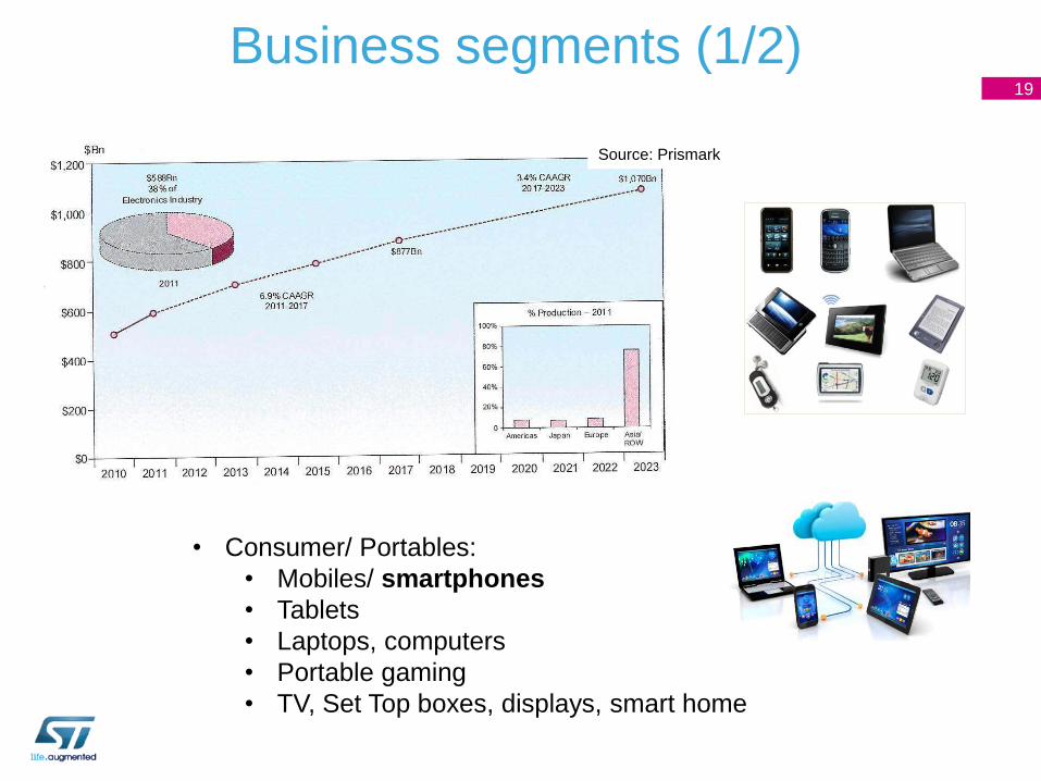
Business segments (1/2) 19
Source: Prismark
• Consumer/ Portables:
• Mobiles/ smartphones
• Tablets
• Laptops, computers
• Portable gaming
• TV, Set Top boxes, displays, smart home
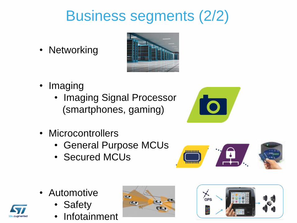
Business segments (2/2)
• Networking
• Imaging
• Imaging Signal Processor
(smartphones, gaming)
• Microcontrollers
• General Purpose MCUs
• Secured MCUs
• Automotive
• Safety
• Infotainment
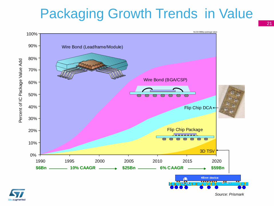
0%
10%
20%
30%
40%
50%
60%
70%
80%
90%
100%
1990 1995 2000 2005 2010 2015 2020
Kc210.088bp package value
IC PACKAGE VALUE TRENDP
erc
en
t o
f IC
Packag
e V
alu
e A
dd
Wire Bond (Leadframe/Module)
Wire Bond (BGA/CSP)
Flip Chip DCA
Flip Chip Package
3D TSV
$6Bn 10% CAAGR 6% CAAGR$25Bn $59Bn
Source: Prismark
21
Packaging Growth Trends in Value
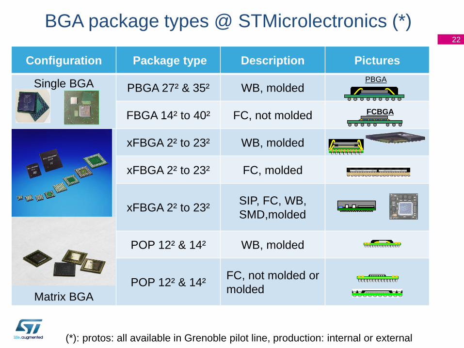
BGA package types @ STMicrolectronics (*)
Configuration Package type Description Pictures
Single BGA PBGA 27² & 35² WB, molded
FBGA 14² to 40² FC, not molded
Matrix BGA
xFBGA 2² to 23² WB, molded
xFBGA 2² to 23² FC, molded
xFBGA 2² to 23² SIP, FC, WB,
SMD,molded
POP 12² & 14² WB, molded
POP 12² & 14² FC, not molded or
molded
22
PBGA
FCBGA
(*): protos: all available in Grenoble pilot line, production: internal or external
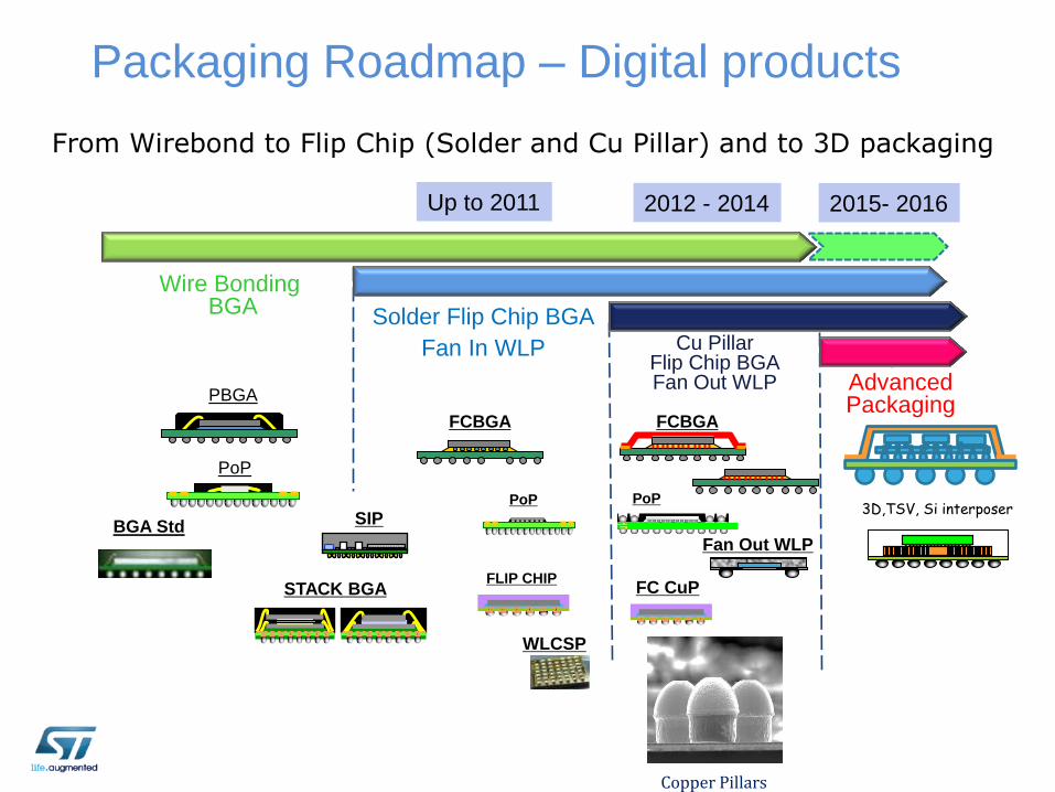
Packaging Roadmap – Digital products
SIP
Emerging
technologies
STACK BGA
BGA Std
FLIP CHIP
WLCSP
FC CuP
Solder Flip Chip BGA
Fan In WLP Cu Pillar Flip Chip BGA Fan Out WLP
Wire Bonding BGA
3D Advanced Packaging
Fan Out WLP
PBGA
FCBGA FCBGA
From Wirebond to Flip Chip (Solder and Cu Pillar) and to 3D packaging
Up to 2011 2012 - 2014 2015- 2016
Copper Pillars
PoP
PoP
PoP 3D,TSV, Si interposer
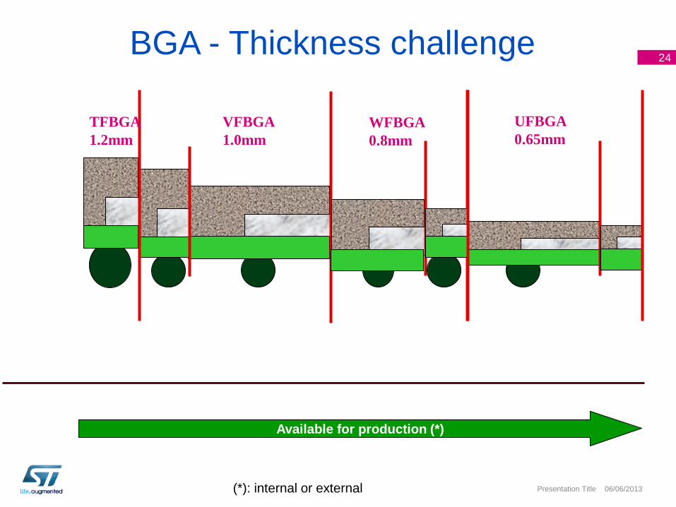
BGA - Thickness challenge 24
06/06/2013 Presentation Title
VFBGA
1.0mm
UFBGA
0.65mm
WFBGA
0.8mm
TFBGA
1.2mm
Available for production (*)
(*): internal or external
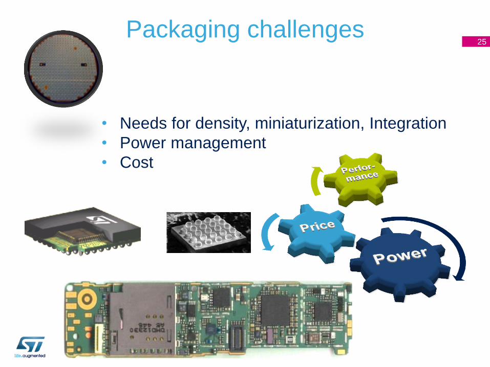
• Needs for density, miniaturization, Integration
• Power management
• Cost
25 Packaging challenges
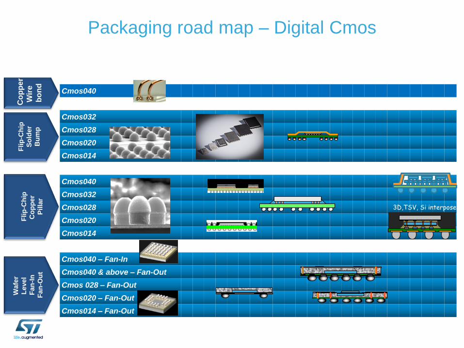
Packaging road map – Digital Cmos
Cmos040
Cmos032
Cmos028
Cmos020
Cmos014
Cmos040
Cmos032
Cmos028
Cmos020
Cmos014
Cmos040 – Fan-In
Cmos040 & above – Fan-Out
Cmos 028 – Fan-Out
Cmos020 – Fan-Out
Cmos014 – Fan-Out
Co
pp
er
Wir
e
bo
nd
F
lip
-Ch
ip
So
lde
r
Bu
mp
Flip
-Ch
ip
Co
pp
er
Pilla
r
Wa
fer
Le
ve
l
Fa
n-I
n
Fa
n-O
ut
3D,TSV, Si interposer
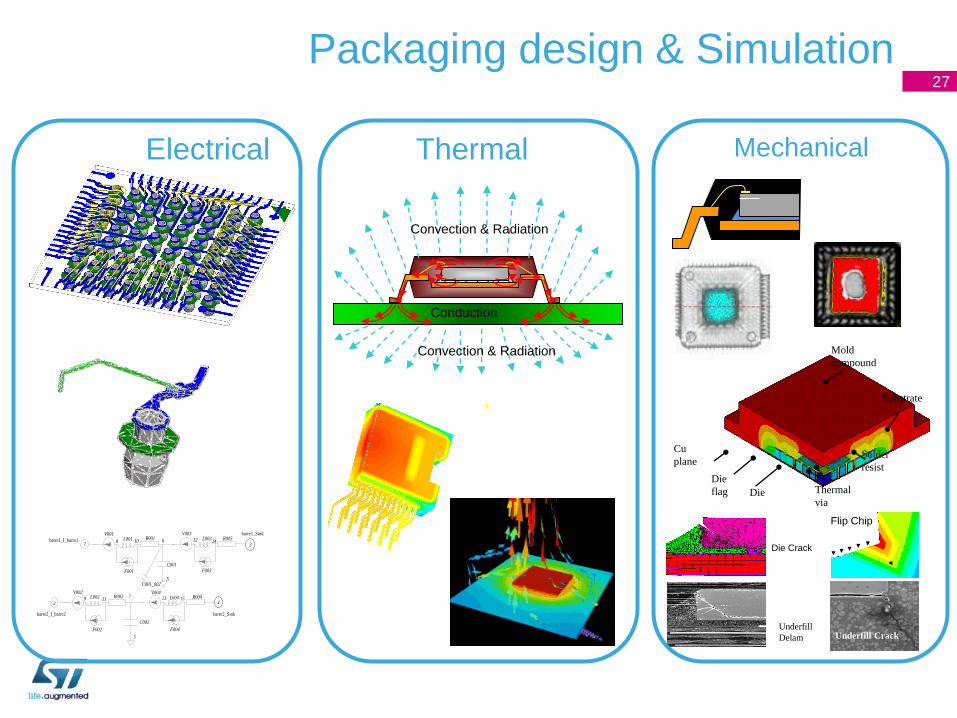
3D structure extraction
Packaging design & Simulation
V001 V003
V004
F003C001
2 4
1 38 10 6 12 14
9 11 7 13 15
5
5
V002
F001
F002 F004
C002
L001
L002
L003
L004
R001 R003
R002 R004
C001_002
barre1_I_barre1
barre2_I_barre2
barre1_Sink
barre2_Sink
Electrical
Convection & Radiation
Convection & Radiation
Conduction
Thermal
Flip - chip
underfill
Flip
Flip - chip
Underfill Crack
Die Crack
Flip Chip
Underfill
Delam
Mold
compound
Solder
resist
Thermal
via
Cu
plane
Die
flag Die
Substrate
Mechanical
27
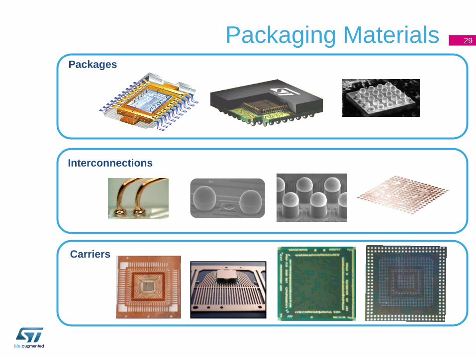
• Materials in packaging play key roles in
• Performance • Power consumption and dissipation • Price
• 2 major materials in any packages: • Carriers: Leadframes / Substrates • Interconnects: wires, bumps, RDL
• The right choice of materials for an optimized 3Ps
• Interactions with die and carriers
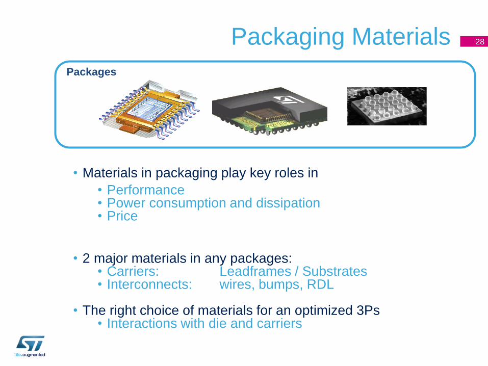
28 Packaging Materials
Packages
Interconnections
Carriers
29 Packaging Materials Packages
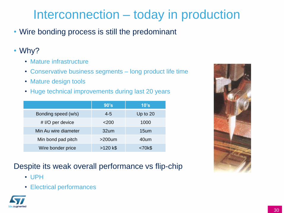
Interconnection – today in production
• Wire bonding process is still the predominant
• Why?
• Mature infrastructure
• Conservative business segments – long product life time
• Mature design tools
• Huge technical improvements during last 20 years
Despite its weak overall performance vs flip-chip
• UPH
• Electrical performances
30
90’s 10’s
Bonding speed (w/s) 4-5 Up to 20
# I/O per device <200 1000
Min Au wire diameter 32um 15um
Min bond pad pitch >200um 40um
Wire bonder price >120 k$ <70k$
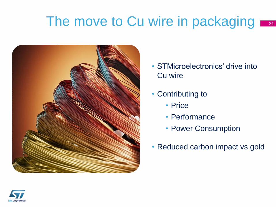
The move to Cu wire in packaging 31
• STMicroelectronics’ drive into
Cu wire
• Contributing to
• Price
• Performance
• Power Consumption
• Reduced carbon impact vs gold
Leading in Copper 32
• Addressing the challenges of
various technologies
• In high volume production
2009 : Length of gold wire converted
to copper can circle the earth!
2012 : Length of gold wire
converted to copper can
reach the moon! Achieved!
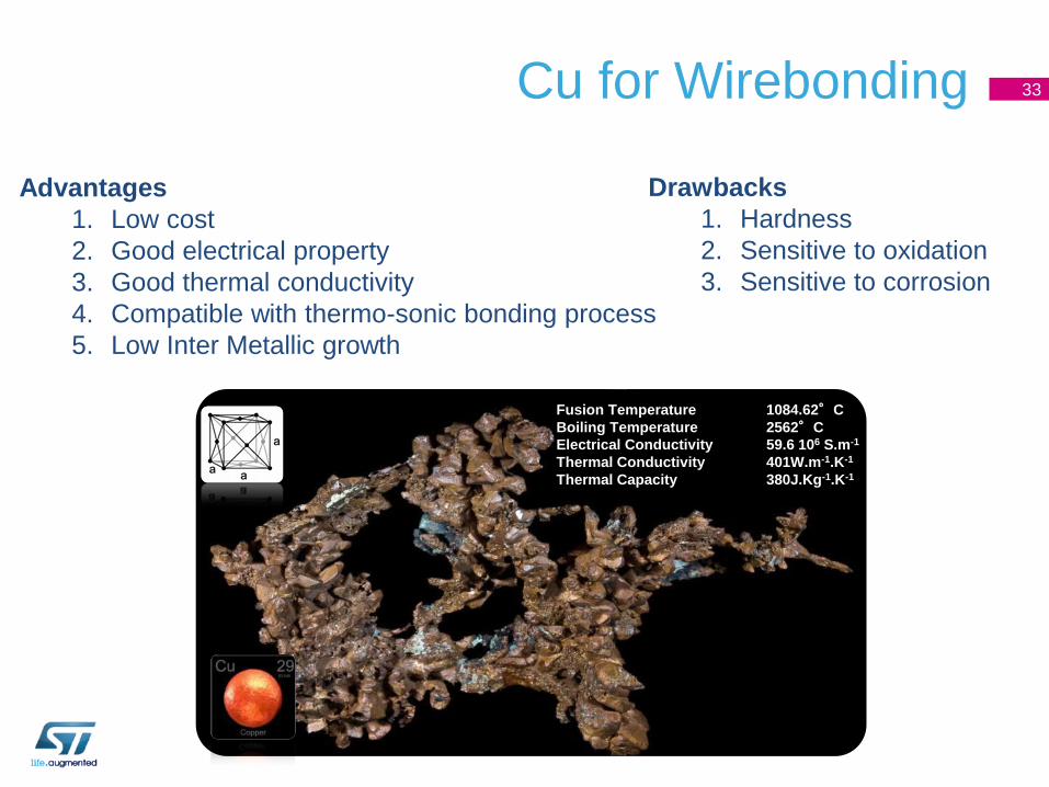
Fusion Temperature 1084.62°C
Boiling Temperature 2562°C
Electrical Conductivity 59.6 106 S.m-1
Thermal Conductivity 401W.m-1.K-1
Thermal Capacity 380J.Kg-1.K-1
Advantages
1. Low cost
2. Good electrical property
3. Good thermal conductivity
4. Compatible with thermo-sonic bonding process
5. Low Inter Metallic growth
Drawbacks
1. Hardness
2. Sensitive to oxidation
3. Sensitive to corrosion
Cu for Wirebonding 33
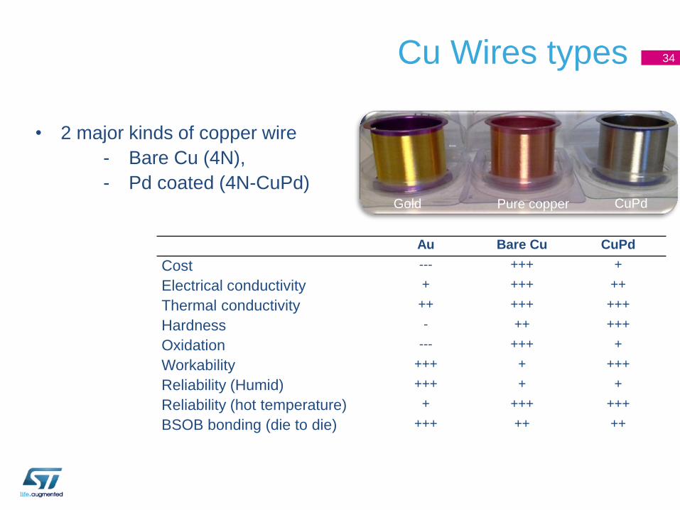
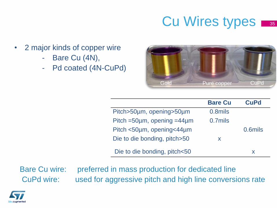
Cu Wires types
Gold Pure copper CuPd
Au Bare Cu CuPd
Cost --- +++ +
Electrical conductivity + +++ ++
Thermal conductivity ++ +++ +++
Hardness - ++ +++
Oxidation --- +++ +
Workability +++ + +++
Reliability (Humid) +++ + +
Reliability (hot temperature) + +++ +++
BSOB bonding (die to die) +++ ++ ++
• 2 major kinds of copper wire
- Bare Cu (4N),
- Pd coated (4N-CuPd)
34
Cu Wires types
Bare Cu CuPd
Pitch>50µm, opening>50µm 0.8mils
Pitch =50µm, opening =44µm 0.7mils
Pitch <50µm, opening<44µm 0.6mils
Die to die bonding, pitch>50 x
Die to die bonding, pitch<50 x
Bare Cu wire: preferred in mass production for dedicated line
CuPd wire: used for aggressive pitch and high line conversions rate
35
Gold Pure copper CuPd
• 2 major kinds of copper wire
- Bare Cu (4N),
- Pd coated (4N-CuPd)
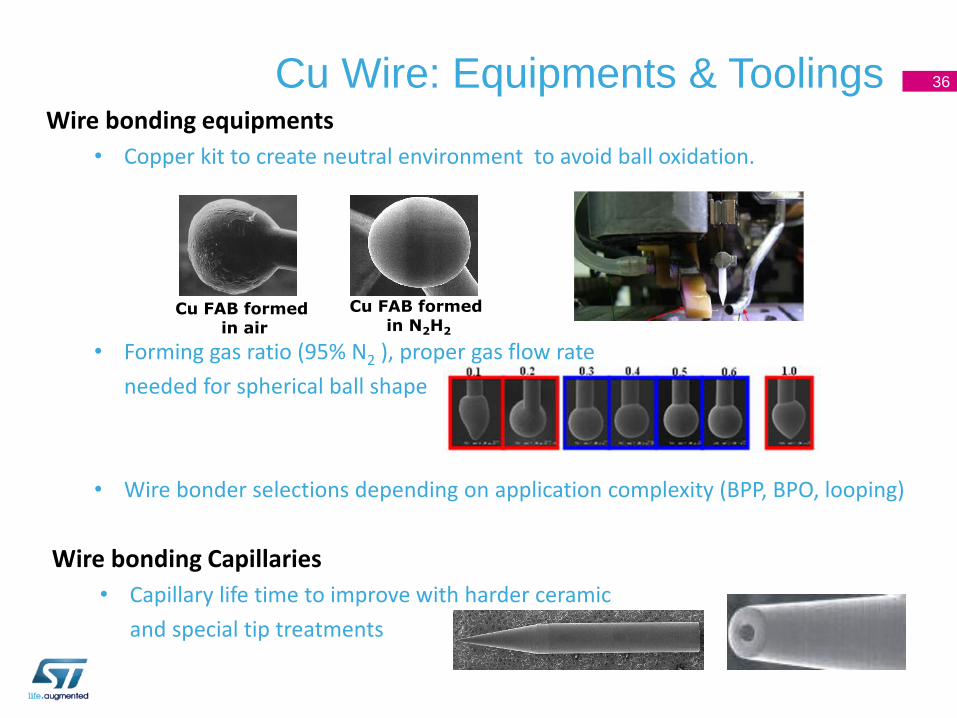
Cu Wire: Equipments & Toolings Wire bonding equipments
• Copper kit to create neutral environment to avoid ball oxidation.
• Forming gas ratio (95% N2 ), proper gas flow rate
needed for spherical ball shape
• Wire bonder selections depending on application complexity (BPP, BPO, looping)
Cu FAB formed in air
Cu FAB formed in N2H2
36
Wire bonding Capillaries
• Capillary life time to improve with harder ceramic
and special tip treatments
0
2,000
4,000
6,000
8,000
10,000
12,000
2003 2004 2005 2006 2007 2008 2009 2010 2011 2012
Cumulated M units produced in Cu wire
Year
BGA
Hi-Quad
PDIP
Power Plastic
PowerSO
PowerSSO
QFN
QFP
SIL
SMD Flat Diodes
SO
TSSOP
Watts
By Package:
Billions of parts produced in Cu Wire
Wide variety of Packages & Applications 37
PowerSO
PowerSSO
SMD Flat Diodes
Hi-Quad
QFP
QFN
SO
PDIP
BGA
Power
Plastic
&
Watts
• Industrial
• Consumer
• Wireless
• Computers & Peripherals
• Automotive
Cumulated M Units
produced in Cu wire
TSSOP
0
500
1,000
1,500
2,000
2,500
2003 2004 2005 2006 2007 2008 2009 2010 2011 2012 EndMay
M units produced in Cu wire / year
Year
BGA
Hi-Quad
PDIP
Power Plastic
PowerSO
PowerSSO
QFN
QFP
SIL
SMD Flat Diodes
SO
TSSOP
Watts
By Package:
38
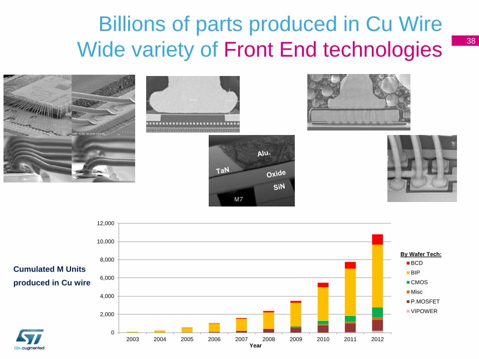
Billions of parts produced in Cu Wire
Wide variety of Front End technologies
Cumulated M Units
produced in Cu wire
0
2,000
4,000
6,000
8,000
10,000
12,000
2003 2004 2005 2006 2007 2008 2009 2010 2011 2012
Cumulated M units produced in Cu wire
Year
BCD
BIP
CMOS
Misc
P.MOSFET
VIPOWER
By Wafer Tech:
0
100,000
200,000
300,000
400,000
500,000
600,000
700,000
800,000
2001 2002 2003 2004 2005 2006 2007 2008 2009 2010 2011 2012
Cumulated km ofpurchased Cu wires
Year
3
2.5
2
1.5
1.3
1.2
1
0.8
0.7
0.6
By Dia (mil)By Dia (mil)By Dia (mil)
39
Thousands of Kms of Cu Wire
Wide variety of Wire types
Cumulated km of
purchased Cu wires
2 – 2.5 – 3mils
< 1mil
0.6mil
Earth's Circumference :
40 000 km
Earth-Moon:
~400 000 km
40
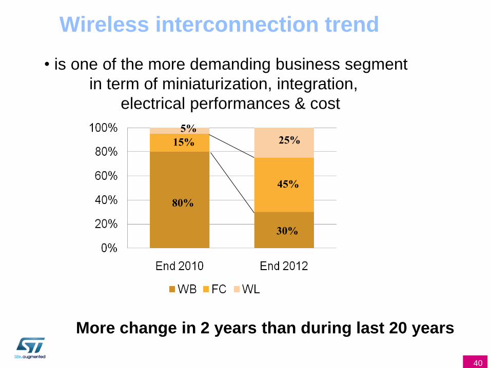
Wireless interconnection trend
• is one of the more demanding business segment
in term of miniaturization, integration,
electrical performances & cost
More change in 2 years than during last 20 years
80%
15%
30%
5%
45%
25%
41
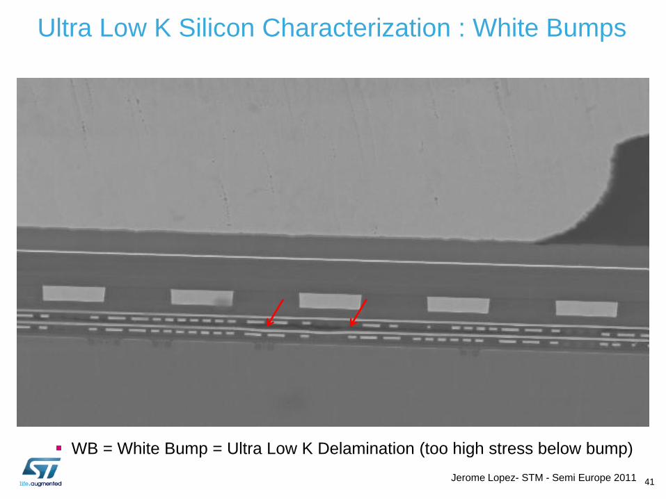
Ultra Low K Silicon Characterization : White Bumps
WB = White Bump = Ultra Low K Delamination (too high stress below bump)
Jerome Lopez- STM - Semi Europe 2011
The larger the die, the more CTE stress mismatch (die to substrate)
The more space available for pad pitch solder bumps rather than Pillars
42
Flip Chip Process: Mass Reflow (Capillary UnderFill)
vs TC-NCP (Thermo-Compression)
Thermo Compression Cu Pillar, Pitch ≥ 50µm (40um for 3D)
No reflow, vertical stress with Thermo-Compression bond force
NCPaste applied before die attach, absorbing part of stress.
Miniaturization
Reliability & Yield
Higher bump density &
finer bump pitch <80um
Substrate Cost & Layout
Assy Cost & UPH
Lower Sourcing flexibility
Mass Reflow Solder, Pitch ≥ 140µm
Low stress due to large UBM & soft solder bump material
Mature (process,materials)
Lower stress (soft bump,
larger UBM)
Sourcing flexibility
Substrate Cost (more
layers, SOP) & Layout
Large bump pitch
PROS CONS
Die area (mm2)
Cu pillars
Fine
Pitch
Solder Bumps
Large
Pitch
Cu pillars
Fine
Pitch
MR
MR
TC
Cu pillars
Large
Pitch
MR
Reflow generates stress for bumps during cooling :
Si & Substrate have ≠ CTE, stress on bumps without protection
Mature (process,materials)
Substrate & Assy Cost
Sourcing flexibility
Higher stress at
bump area
Sensitive to unsolder
Mass Reflow Cu Pillar, Pitch ≥ 80µm
Stress induced by Cu Pillar is reduced thanks to
usage of very large UBM size
Mass Reflow Cu Pillar, Pitch ≥ 125µm Mature (process,materials)
Limited stress (larger UBM)
Reduce O/S risk vs Solder
Current density per bump
Sourcing flexibility
Substrate Cost (same
as Solder Bump one)
Large bump pitch &
UBM size
Stress
Reduction
LA
RG
E P
ITC
H / B
UM
PS
F
INE
PIT
CH
/ B
UM
PS
Cu pillars
Fine
Pitch
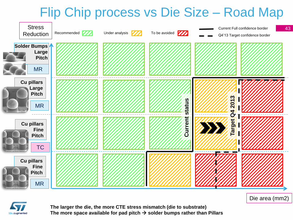
Flip Chip process vs Die Size – Road Map
The larger the die, the more CTE stress mismatch (die to substrate)
The more space available for pad pitch solder bumps rather than Pillars
Solder Bumps
Large
Pitch
Cu pillars
Fine
Pitch
MR
MR
TC
43 To be avoided Under analysis Recommended
Current Full confidence border
Q4’13 Target confidence border
Cu pillars
Large
Pitch
MR
Cu
rre
nt
sta
tus
Targ
et
Q4 2
013
Die area (mm2)
Stress
Reduction
44
Al SiN
Si
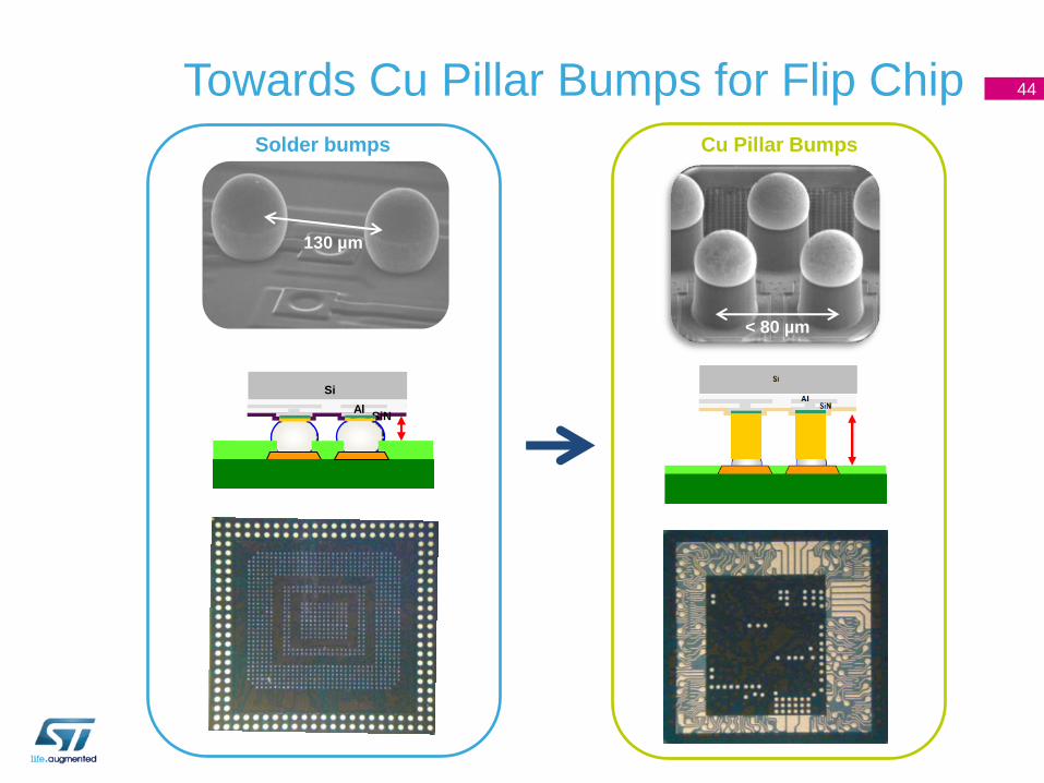
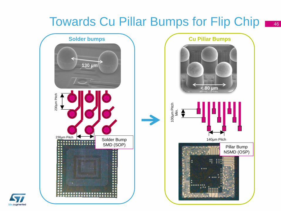
Towards Cu Pillar Bumps for Flip Chip
130 µm
Solder bumps Cu Pillar Bumps
< 80 µm
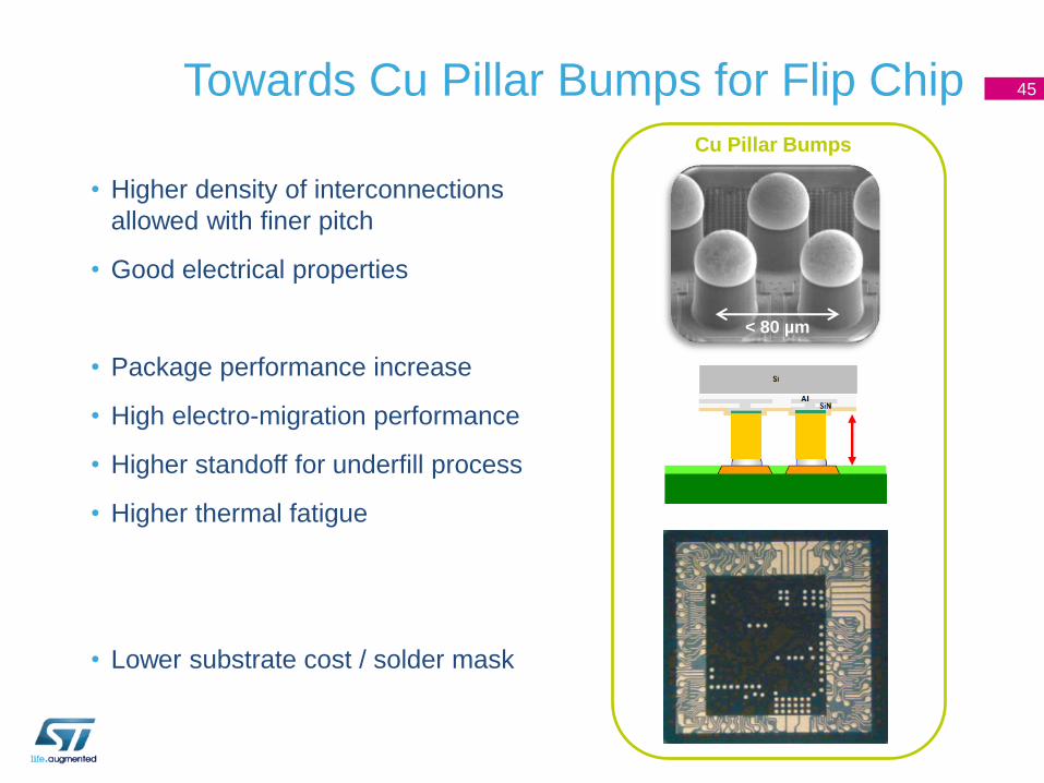
45 Towards Cu Pillar Bumps for Flip Chip
Cu Pillar Bumps
< 80 µm
• Higher density of interconnections
allowed with finer pitch
• Good electrical properties
• Package performance increase
• High electro-migration performance
• Higher standoff for underfill process
• Higher thermal fatigue
• Lower substrate cost / solder mask
46 Towards Cu Pillar Bumps for Flip Chip
130 µm
Solder bumps Cu Pillar Bumps
< 80 µm
230µm Pitch
230µ
m P
itch
Solder Bump
SMD (SOP)
10
0µ
m P
itch
Min
.
140µm Pitch
Pillar Bump
NSMD (OSP)
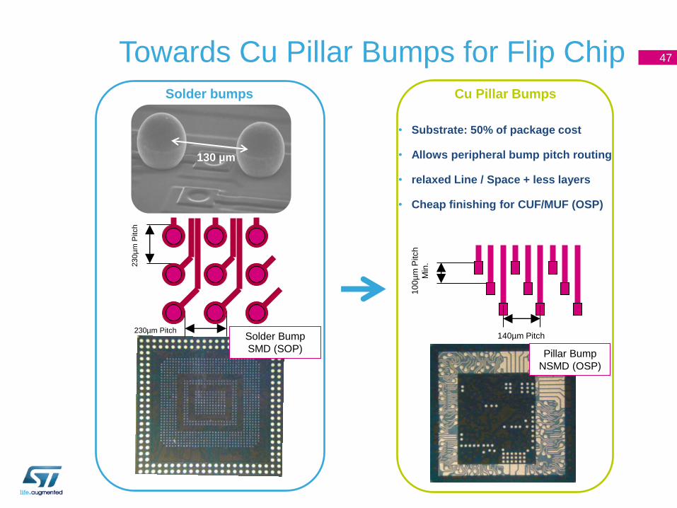
47 Towards Cu Pillar Bumps for Flip Chip
130 µm
Solder bumps Cu Pillar Bumps
230µm Pitch
230µ
m P
itch
Solder Bump
SMD (SOP)
10
0µ
m P
itch
Min
.
140µm Pitch
Pillar Bump
NSMD (OSP)
• Substrate: 50% of package cost
• Allows peripheral bump pitch routing
• relaxed Line / Space + less layers
• Cheap finishing for CUF/MUF (OSP)
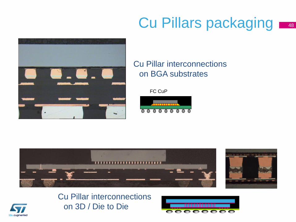
Cu Pillars packaging
Cu Pillar interconnections
on BGA substrates
48
FC CuP
Cu Pillar interconnections
on 3D / Die to Die
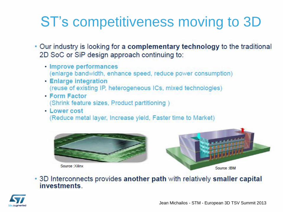
ST’s competitiveness moving to 3D
Jean Michailos - STM - European 3D TSV Summit 2013
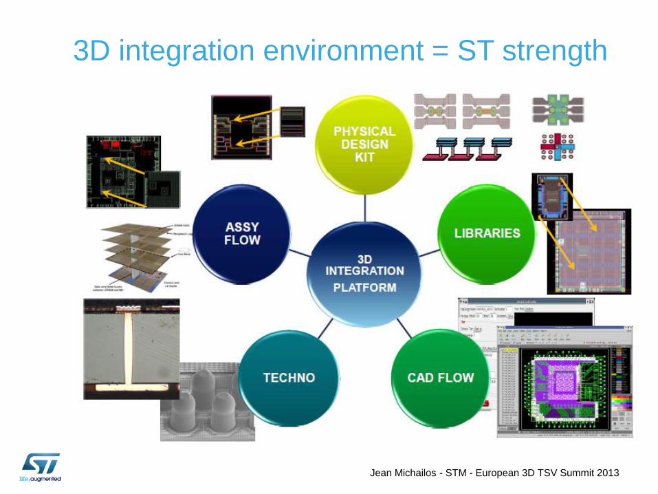
3D integration environment = ST strength
Jean Michailos - STM - European 3D TSV Summit 2013
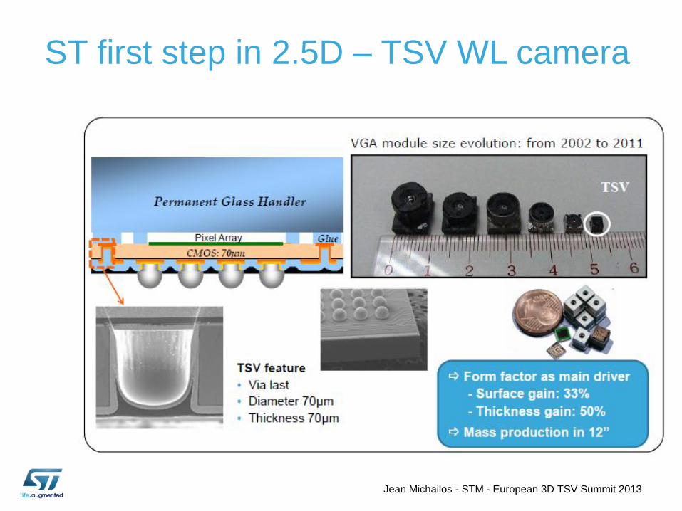
ST first step in 2.5D – TSV WL camera
Jean Michailos - STM - European 3D TSV Summit 2013
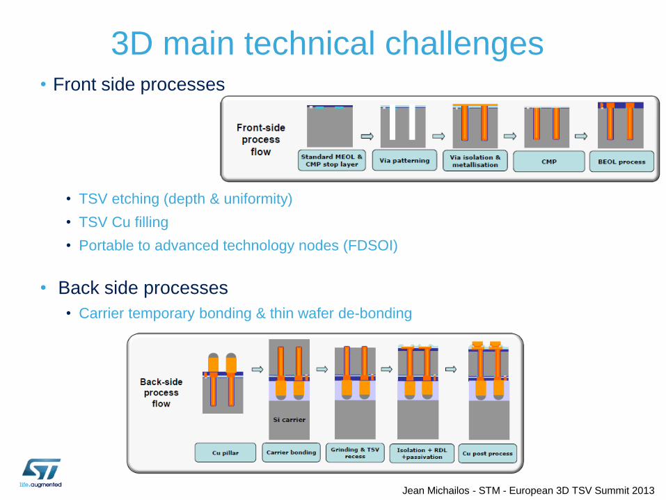
3D main technical challenges • Front side processes
• TSV etching (depth & uniformity)
• TSV Cu filling
• Portable to advanced technology nodes (FDSOI)
• Back side processes
• Carrier temporary bonding & thin wafer de-bonding
Jean Michailos - STM - European 3D TSV Summit 2013
3D main technical challenges
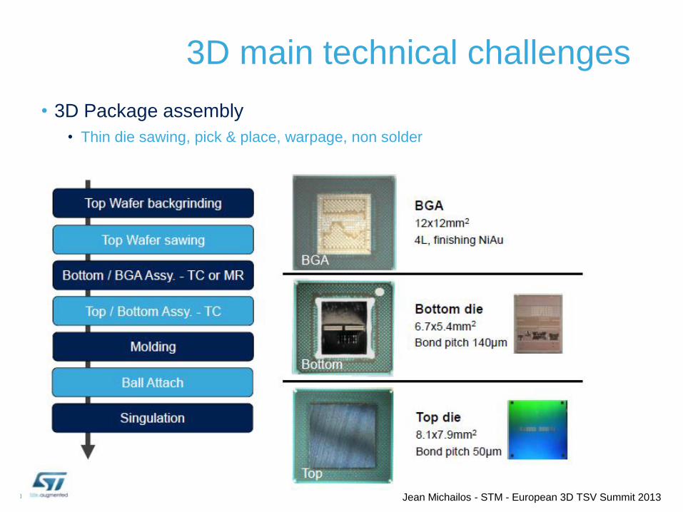
• 3D Package assembly
• Thin die sawing, pick & place, warpage, non solder
Jean Michailos - STM - European 3D TSV Summit 2013
Analog/digital partitioning
Jean Michailos - STM - European 3D TSV Summit 2013
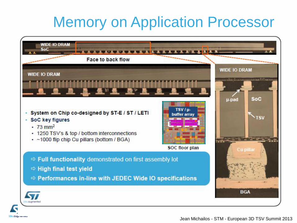
Memory on Application Processor
Jean Michailos - STM - European 3D TSV Summit 2013
Further development axes
Jean Michailos - STM - European 3D TSV Summit 2013
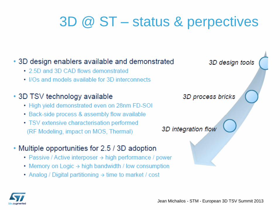
3D @ ST – status & perpectives
Jean Michailos - STM - European 3D TSV Summit 2013
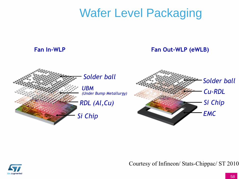
Wafer Level Packaging
58
Solder ball
Cu-RDL
Si Chip
EMC
UBM (Under Bump Metallurgy)
RDL (Al,Cu)
Si Chip
Solder ball
Fan In-WLP Fan Out-WLP (eWLB)
Courtesy of Infineon/ Stats-Chippac/ ST 2010
Fan-out WLP / 2-side
59
Pre-formed PCB Bar
Laser drill and pasted filling
180um
45
0u
m
ePOP Package ePOP X-section
8x8 Fan-out
12x12 Fan-out
60
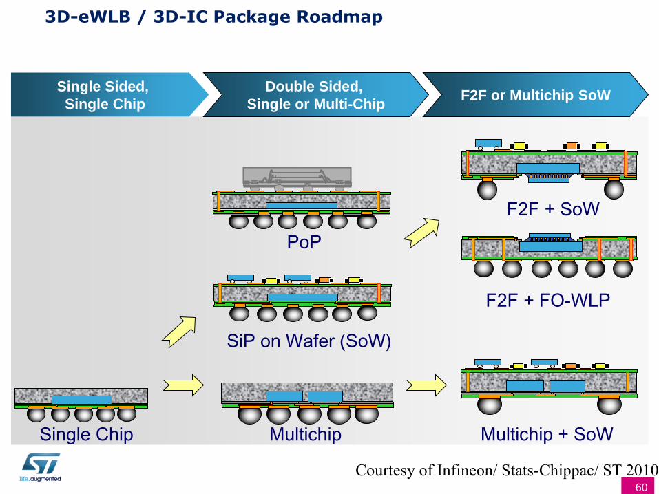
Single Chip
F2F + SoW
F2F + FO-WLP
Multichip + SoW
Single Sided,
Single Chip
Double Sided,
Single or Multi-Chip F2F or Multichip SoW
Multichip
SiP on Wafer (SoW)
PoP
3D-eWLB / 3D-IC Package Roadmap
Courtesy of Infineon/ Stats-Chippac/ ST 2010
WLPs WB BGAs Sensors FC BGAs 3D IC
The Interconnections trends for new Packaging
Power Adv. QFNs
Sense & Power Digital
Cu Pillars
Cu wires
Inte
rconnections
Cu RDL
61
Content
• STMicroelectronics presentation • General presentation
• R&D Packaging @ STM
• Packaging Platforms covered at ST
• Packaging development for Advanced Cmos technologies • Business segments
• Main requests
• Cu pillar for FC packages
• Cu RDL for WLPs…
• Conclusions
62
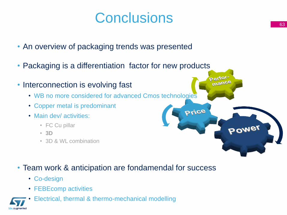
• An overview of packaging trends was presented
• Packaging is a differentiation factor for new products
• Interconnection is evolving fast
• WB no more considered for advanced Cmos technologies
• Copper metal is predominant
• Main dev/ activities:
• FC Cu pillar
• 3D
• 3D & WL combination
• Team work & anticipation are fondamendal for success
• Co-design
• FEBEcomp activities
• Electrical, thermal & thermo-mechanical modelling
63 Conclusions
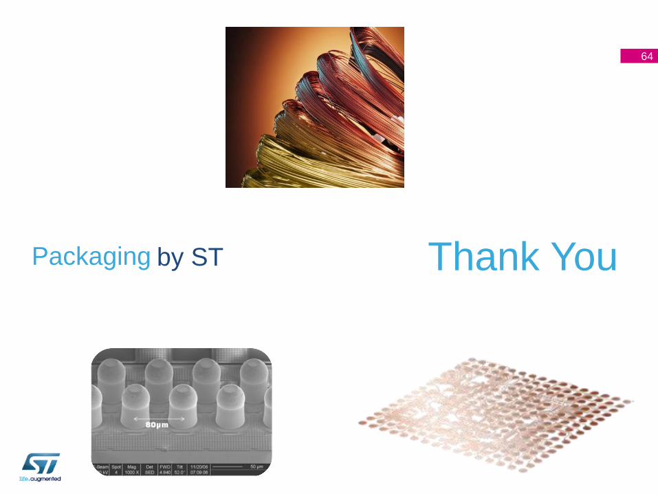
Packaging
64
by ST Thank You