Technical Reference Note Rev.06.18.20_#1.7 DS1100SLPE-3 Series Page 1 DS1100SLPE-3 1100 Watts Distributed Power Total Power: 1100 Watts Input Voltage: 90 to 264 Vac # of Outputs: Main and Standby Special Features • 1100 W output power • High-power and short form factor • 1U power supply • High-density design: 26 W/in 3 • Active Power Factor Correction • EN61000-3-2 harmonic compliance • 80plus Platinum Efficiency • Inrush current control • N+1 or N+N Redundant • Hot-pluggable • Active current sharing • Full digital control • PMBus compliant • Accurate input power reporting • Compatible with Artesyn’s Universal PMBus GUI • Reverse airflow option • Two-year warranty Safety UL/cUL 62368-1 (UL Recognized) DEMKO+ CB Report EN62368-1 CE Mark China CCC BSMI Product Descriptions DS1100SLPE-3 series power supply accepts a wide range 90-264 Vac input and provides a main 12 V output and a 3.3 V standby output, rated at 1,100 watts. It is an 80 Plus Platinum supply with a high peak efficiency of 94%. Housed in an industry standard 1U x 2.1 inch rack-mounting package, the power supply is ideal for space-constrained applications. This series comes in two airflow versions - dc-connector to ac-connector and vice versa. The main 12 V output can deliver up to 90 A and stay within regulation down to zero load, making it perfect for feeding downstream DC-DC converters in systems that use distributed power architectures (DPA). Active current sharing enables multiple supplies to be paralleled for very high current applications without need of additional components. The power supply is hot pluggable and ideal for fault tolerant, N+1 and N+N redundant applications. This digitally-controlled power supply is PMBus™ compliant. A built-in I2C serial interface allows set-up, monitoring and control to be performed using Artesyn Embedded Technologies' universal PMBus graphical user interface.
Transcript
Technical Reference Note
Rev.06.18.20_#1.7DS1100SLPE-3 Series
Page 1
DS1100SLPE-3
1100 Watts
Distributed Power
Total Power: 1100 Watts
Input Voltage: 90 to 264 Vac
# of Outputs: Main and Standby
Special Features• 1100 W output power
• High-power and short form factor
• 1U power supply
• High-density design: 26 W/in3
• Active Power Factor Correction
• EN61000-3-2 harmonic
compliance
• 80plus Platinum Efficiency
• Inrush current control
• N+1 or N+N Redundant
• Hot-pluggable
• Active current sharing
• Full digital control
• PMBus compliant
• Accurate input power reporting
• Compatible with Artesyn’s
Universal PMBus GUI
• Reverse airflow option
• Two-year warranty
SafetyUL/cUL 62368-1 (UL Recognized)
DEMKO+ CB Report EN62368-1
CE Mark
China CCC
BSMI
Product DescriptionsDS1100SLPE-3 series power supply accepts a wide range 90-264 Vac input and provides a main 12 V output and a 3.3 V standby output, rated at 1,100 watts. It is an 80 Plus Platinum supply with a high peak efficiency of 94%. Housed in an industry standard 1U x 2.1 inch rack-mounting package, the power supply is ideal for space-constrained applications. This series comes in two airflow versions - dc-connector to ac-connector and vice versa.
The main 12 V output can deliver up to 90 A and stay within regulation down to zero load, making it perfect for feeding downstream DC-DC converters in systems that use distributed power architectures (DPA). Active current sharing enables multiple supplies to be paralleled for very high current applications without need of additional components. The power supply is hot pluggable and ideal for fault tolerant, N+1 and N+N redundant applications.
This digitally-controlled power supply is PMBus™ compliant. A built-in I2C serial interface allows set-up, monitoring and control to be performed using ArtesynEmbedded Technologies' universal PMBus graphical user interface.
Technical Reference NoteTechnical Reference Note
Rev.06.18.20_#1.7DS1100SLPE-3 Series
Page 2
Model Numbers
Options
None
Standard Output Voltage Minimum Load Maximum LoadStandbySupply
Maximum Output Power (Main + Standby) All models PO,max - - 1100 W
Isolation VoltageInput to outputs
Input to safety groundAll modelsAll models
--
--
42432951
VdcVdc
Ambient Operating Temperature DS1100SLPE-3DS1100SLPE-3-001
TA
-5-5
--
+651
+551OC
Storage Temperature All models TSTG -40 - +85 OC
Humidity (non-condensing)Operating
Non-operatingAll modelsAll models
55
--
9095
%%
AltitudeOperating
Non-operatingAll models
--
--
10,00050,000
feetfeet
MTBF2 All models 500 - - KHr
Note 1 - DS1100SLPE-3: 1100W from -5 to 50OC, withstand operation up to 65OC at 660W output power without damage.
DS1100SLPE-3-001: 1100W from -5 to 45OC, withstand operation up to 55OC at 660W output power without damage.
Note 2 - Telcordia Issue 3 at full load, 40OC
Electrical Specifications
Absolute Maximum Ratings
Stress in excess of those listed in the “Absolute Maximum Ratings” may cause permanent damage to the power supply. These are stress ratings only and functional operation of the unit is not implied at these or any other conditions above those given in the operational sections of this TRN. Exposure to any absolute maximum rated condition for extended periods may adversely affect the power supply’s reliability.
Technical Reference NoteTechnical Reference Note
Rev.06.18.20_#1.7DS1100SLPE-3 Series
Page 4
Input Specifications
Table 2. Input Specifications:
Parameter Conditions Symbol Min Typ Max Unit
Operating Input Voltage, AC All VIN,AC 90 115/230 264 Vac
Input AC Frequency All fIN,AC 47 50/60 63 Hz
Maximum Input Current(IO = IO,max, ISB = ISB,max)
VIN,AC = 90Vac IIN,max - - 14.5 A
No Load Input Power(VO = On, IO = 0A, ISB = 0A)
All PIN,no-load - - 15 W
No Load Input Current(VO = On, IO = 0A, ISB = 0A)
All IIN,no-load - - 200 mA
Harmonic Line Currents All THD Per EN61000-3-2
Power Factor 20% load and above PF 0.9 - -
Startup Surge Current (Inrush)Cold-startHot-start
VIN,AC = 264Vac IIN,surge--
--
5535
A
Input FuseInternal, 5x20mm, Quick Acting 16A,
250V- 16 - A
Leakage Current to Earth GroundVIN,AC = 264VacfIN,AC = 50/60Hz
- - 1.75 mA
Operating Efficiency1
VIN,AC = 230VacIO = 10% IO,max
IO = 20% IO,max
IO = 50% IO,max
IO = 100% IO,max
η
80909491
----
----
%%%%
System StabilityPhase Margin
Gain Margin45-
--6
--
ØdB
Note 1 - DS1100SLPE-3 is certified for 80plus Platinum Efficiency level at 230Vac. The loading conditions are defined according to CSCI criteria.
Technical Reference NoteTechnical Reference Note
Rev.06.18.20_#1.7DS1100SLPE-3 Series
Page 5
Table 3. Output Specifications:
Parameter Conditions Symbol Min Typ Max Unit
Factory Set Voltage All%VO -1 - +1
%%VSB -1 - +1
Output RegulationInclusive of set-point, temperature change,
warm-up drift
VO 11.4 12.0 12.6
Vdc
VSB 3.14 3.3 3.46
Output Ripple, pk-pk
Measure with a 0.1uFceramic capacitor in parallel with a 10uF
tantalum capacitor, 0 to 20MHz bandwidth.
A resistor load is recommended.
VO - - 180
mVPK-PK
VSB - - 80
Output Current1 AllIO 5.0 - 90.0
AISB 0.0 - 3.0
VO Current Share Accuracy 25% to 100% IO,max -5.625 - 5.625 A
Minimum Load for Current Sharing All 7 - - %IO,max
Number of Parallel UnitsMain Output “ISHARE”
connected- - 6 Unit
Load Capacitance Start upVO 500 - 11,000 uF
VSB 20 - 1000 uF
VO Dynamic Load ResponsePeak Deviation2
50% load change, slew rate = 1A/uS
±%VO -5 - 5 %
VO Dynamic Load ResponseSetting Time
50% load change, slew rate = 1A/uS
TS - 500 - uSec
VO Long Term StabilityMax change over 24 hours
After thermal equilibrium (30 mins)VIN,AC = 100/200Vac
±%VO -0.5 - 0.5 %
Note 1 - No load operation will not cause any damage to the power supply. Overshoot/undershoot limits do not apply duringturn-on/turn-off at no load condition.
Note 2 - Minimum allowable output capacitance of 500uF during this test.
Output Specifications
Technical Reference NoteTechnical Reference Note
Rev.06.18.20_#1.7DS1100SLPE-3 Series
Page 6
System Timing Specifications
Table 4. System Timing Specifications:
Label Parameter Min Typ Max Unit
T1 Delay from AC being applied to VSB being within regulation - - 2500 mSec
T2Delay from Standby output to main output voltage being within regulation.
- - 1000 mSec
T3Delay from AC being applied to main output voltages being within regulation.
- - 3000 mSec
T4Delay from output voltages within regulation limits to PWOK asserted.
100 - 1000 mSec
T5 Delay from loss of AC to deassertion of PWOK 5 - - mSec
T6 Delay from loss of AC to main output falling out of regulation 16 - - mSec
T7 Delay from loss of AC to deassertion of ACOK - - 20 mSec
T81 Delay from loss of AC to Standby output falling out of regulation.
25 - - mSec
T9Delay from deassertion of PWOK to output voltagesfalling out of regulation.
1 - 700 mSec
T10Delay from PS_ON_L assertion to output voltages being within regulation.
- - 400 mSec
Note 1 - T8 is measured with standby output loaded at 1A.
Technical Reference NoteTechnical Reference Note
Rev.06.18.20_#1.7DS1100SLPE-3 Series
Page 7
System Timing Specifications
Note 1 - ACOK can assert earlier than VSB.
Technical Reference NoteTechnical Reference Note
Rev.06.18.20_#1.7DS1100SLPE-3 Series
Page 8
DS1100SLPE-3 Performance Curves
Figure 1: DS1100SLPE-3 Turn-on delay via AC mains - Vin = 90VacFull Load: IO = 90.0A, ISB = 3A
Figure 14: DS1100SLPE-3 Transient Response - Vo Deviation (low to high)50% to 100% load change, 1A/uS slew rate, VIN = 230Vac
Ch 1: VO Ch 2: IO Output capacitance = 500uF
Figure 15: DS1100SLPE-3 Transient Response - Vo Deviation (high to low)100% to 50% load change, 1A/uS slew rate, VIN = 230Vac
Ch 1: VO Ch 2: IO Output capacitance = 500uF
Technical Reference NoteTechnical Reference Note
Rev.06.18.20_#1.7DS1100SLPE-3 Series
Page 11
Protection Function Specification
Input Fusing
DS1100SLPE-3 series power supply is equipped with an internal non user replaceable 16A Fast Acting 250Vac fuse to IEC 127 for fault protection in the L line input.
Over Voltage / Under Voltage Protection (OVP / UVP)
DS1100SLPE-3 series power supply provides latch mode over and under voltage protection as defined by the output under voltage and output over voltage parameters for each output. When the OVP circuit is activated (main output and standby), the power supply must latch off requiring PSON or the input power to be recycled manually to reset the power supply after the fault has been removed.
The power supply will shutdown within 20mSec if the output voltage drops below 20% of the nominal rating for more than 2.5mSec. The power supply will attempt to auto-restart once every 3 seconds.
The under-voltage protection can be disabled during start-up and shutdown transitions. A failure on the reference used for regulating the output voltage should not cause the power supply to lose its ability to protect against over-voltage.
Over Current Protection (OCP)
DS1100SLPE-3 series power supply includes internal current limit circuitry to prevent damage in the event of overload or short circuit. The Main output will be internally protected against output overload or short circuit applied to its output. A fault in the main output will not cause the standby output to shut down. No damage will result to the supply as the result of either short term or long term overloads of the output.
The standby output will have an OCP limit from 110%-150% and will auto-recover when the overload is removed. A fault in the standby output will shutdown other outputs and will auto-recover as well. When the overload on the standby is removed. An OCP fault on the main output will not cause the standby output to fail. The over-current thresholds must be measured under all operating line, load, and temperature conditions.
Parameter Min Nom Max Unit
VO Output Under Voltage 9.6 / / V
VSB Output Under Voltage / / / V
Parameter Min Nom Max Unit
VO Output Over Voltage 13.2 / 14.5 Vdc
VSB Output Over Voltage 3.6 / 3.9 Vdc
Parameter Min Nom Max Unit
VO Output Over Current 107 / 130 %IO,max
VSB Output Over Current 110 / 150 %ISB,max
Technical Reference NoteTechnical Reference Note
Rev.06.18.20_#1.7DS1100SLPE-3 Series
Page 12
Short Circuit Protection (SCP)
DS1100SLPE-3 series power supply protects against a short circuit, which is defined as an impedance of 0.1 ohms or less, applied to any output during start-up or while running will not cause any damage to the power supply (connectors, components, PCB traces, etc.).
When the standby output is shorted, the output will go into “hiccup mode.” When the standby output attempts to restart, the maximum peak current from the output must be less than 10A. The maximum average current, taking into account the “hiccup” duty cycle, must not exceed rated DC output current of the standby.
Over Temperature Protection (OTP)
DS1100SLPE-3 series power supply is internally protected against over temperature conditions. When the OTP limit is reached, all outputs, except standby, will shut down and will remain off until the over temperature condition no longer exists.
A suitable hysteresis point between the OTP threshold and the recovery point will be set to ensure there is no frequent on-off cycling of the outputs. The temperature recovery point will be set well with-in the operating temperature range. Upon reaching the temperature recovery point, all outputs will auto-recover.
Any OTP fault will be reported in the PMBus status flag, without discriminating on which OTP sensing circuit was triggered.
Technical Reference NoteTechnical Reference Note
Rev.06.18.20_#1.7DS1100SLPE-3 Series
Page 13
Mechanical Specifications
Mechanical Outlines
Forward Airflow
Reverse Airflow
Technical Reference NoteTechnical Reference Note
Rev.06.18.20_#1.7DS1100SLPE-3 Series
Page 14
Connector Definitions
AC Input Connector
Pin 1 - L
Pin 2 - N
Pin 3 - Earth Ground
Output Connector - Power Blades
P1-P5 - +12V Return
P6-P10 - 12V
Output Connector - Control Signals
A1 - 3.3VSB
B1 - 3.3VSB
C1 - 3.3VSB
D1 - 3.3VSB
E1 - 3.3VSB
A2 - SGND
B2 - SGND
C2 - Reserved
D2 - Reserved
E2 - Reserved
A3 - A2
B3 - A0
C3 - SDA
D3 - - Remote Sense
E3 - +Remote Sense
A4 - SCL
B4 - PSON_L
C4 - PS_INTERRUPT_L
D4 - A1
E4 - AC_OK
A5 - PSKILL_L
B5 - ISHARE
C5 - PWOK
D5 - Reserved
E5 - PS_PRESENT_L
Power Supply Output Card Edge
L
Earth Ground
N
Technical Reference NoteTechnical Reference Note
Rev.06.18.20_#1.7DS1100SLPE-3 Series
Page 15
Power / Signal Mating Connectors and Pin Types
Table 5. Mating Connectors for DS1100SLPE-3 series
Reference On Power SupplyMating Connectoror Equivalent
AC Input Connector IEC320-C14 IEC320-C13
Output Connector TEI 1926736-3TEI 2-1926739-5, 1892787-6 or equivalent
Technical Reference NoteTechnical Reference Note
Rev.06.18.20_#1.7DS1100SLPE-3 Series
Page 16
LED indicator Definition
There are two LEDs on the power supply chassis at the end opposite to the DC output connector. Output LED indicated will be bi-color (green/amber).The status LED conditions is shown on the below table.
Table 6. LED status
Conditions INPUT LED OUTPUT LED (bi-color)
COLOR GREEN AMBER/GREEN
NO AC INPUT TO PSU OFF OFF
AC PRESENT, STBY ON, MAIN OUTPUT OFF ON Blinking Amber, at least 1Hz
MAIN OUTPUT ON ON ON,GREEN
POWER SUPPLY WARNING (Hi-temp) ON Blinking Amber/Green, at 1:1, 1Hz On
POWER SUPPLY WARNING (Slow fan) ON Blinking Amber/Green, at 1:1, 1Hz On
POWER SUPPLY FAILURE (OVP, OTP, FAN FAULT) ON ON, Amber
AC
DC
Technical Reference NoteTechnical Reference Note
Rev.06.18.20_#1.7DS1100SLPE-3 Series
Page 17
Weight
The maximum weight of DS1100SLPE-3 series power supply is 2.43 lbs / 1100 g.
Technical Reference NoteTechnical Reference Note
Rev.06.18.20_#1.7DS1100SLPE-3 Series
Page 18
Environmental Specifications
EMC Immunity
DS1100SLPE-3 series power supply meets the following EMC immunity specifications:
Table 7. Environmental Specifications:
Document Description
FCC 47CFR 15 Subpart B / CISPR 22/ EN55022/EN300386/GR1089, Class A
IEC/EN 61000-4-3 Electromagnetic Compatibility (EMC) - Testing and measurement techniques, Radiated, radio-frequency, electromagnetic field immunity test, Criteria A
IEC/EN 61000-4-4 Electromagnetic Compatibility (EMC) - Testing and measurement techniques, Electrical Fast Transient/Burst Immunity Test. +/-2KV for AC power port Criteria B, +/-0.5KV for DC ports, I/O and signal ports performance Criteria A
IEC/EN 61000-4-5 Electromagnetic Compatibility (EMC) - Testing and measurement techniques: 4KV common mode and 2KV differential mode for AC ports performance criteria B, 2KV common mode and 1KV differential mode for AC ports performance criteria A
IEC/EN 61000-4-6 Electromagnetic Compatibility (EMC) - Testing and measurement techniques - Immunity to conducted disturbances, induced by radio-frequency fields, performance criteria A
IEC/EN 61000-4-11 Electromagnetic Compatibility (EMC) - Testing and measurement techniques : Voltage Dips and Interruptions: >30% reduction for 500ms, Criteria C, >95% reduction at 60% load for 10ms, Criteria A, >95% reduction for 500mS, Criteria C
IEC/EN 61000-4-12 Electromagnetic Compatibility (EMC) - Testing and measurement techniques - Ring wave immunity: 4KV common mode and 2KV differential mode for AC ports performance criteria A, 2KV common mode and 1KV differential mode for AC ports performance criteria A
EN55022 Information Technology Equipment-Immunity Characteristics, Limits and Method of Measurements
Technical Reference NoteTechnical Reference Note
Rev.06.18.20_#1.7DS1100SLPE-3 Series
Page 19
Environmental Specifications
AC Input Sag and Surge
DS1100SLPE-3 series power supply meets the performance criteria requirements as per Table 8 and Table 9 when subjected to AC line sag and surge conditions. The power supply meets the performance criteria requirements at 60% load. When the power supply is loaded more than 60% or the duration is more than ½ cycle, the power supply may regulate between 11.3V to 12.7V.
Table 8. AC Line Surge:
Duration Surge Operating AC voltage
Line Frequency Performance Criteria
Continuous 10% 140/240Vac 50/60 HzNo loss of function or performance
0 to 1/2 AC cycle 30% 115/230Vac 50/60 HzNo loss of function or performance
Table 9. AC Line Sag:
Duration Sag Operating AC voltage
Line Frequency Performance Criteria
Continuous 10% of operating 100/200Vac 50/60 HzNo loss of function or performance
0 to 1/2 AC cycle 60% of operating 100/200Vac 50/60 HzNo loss of function or performance
0 to 1/2 AC cycle 100% of operating 100/200Vac 50/60 HzLoss of function or performance acceptable, self-recoverable
0 to 1 AC cycle 100% of operating 100/200Vac 50/60 HzLoss of function or performance acceptable, self-recoverable
500ms 30% of operating 100/200Vac 50/60 HzLoss of function or performance acceptable, self-recoverable
Technical Reference NoteTechnical Reference Note
Rev.06.18.20_#1.7DS1100SLPE-3 Series
Page 20
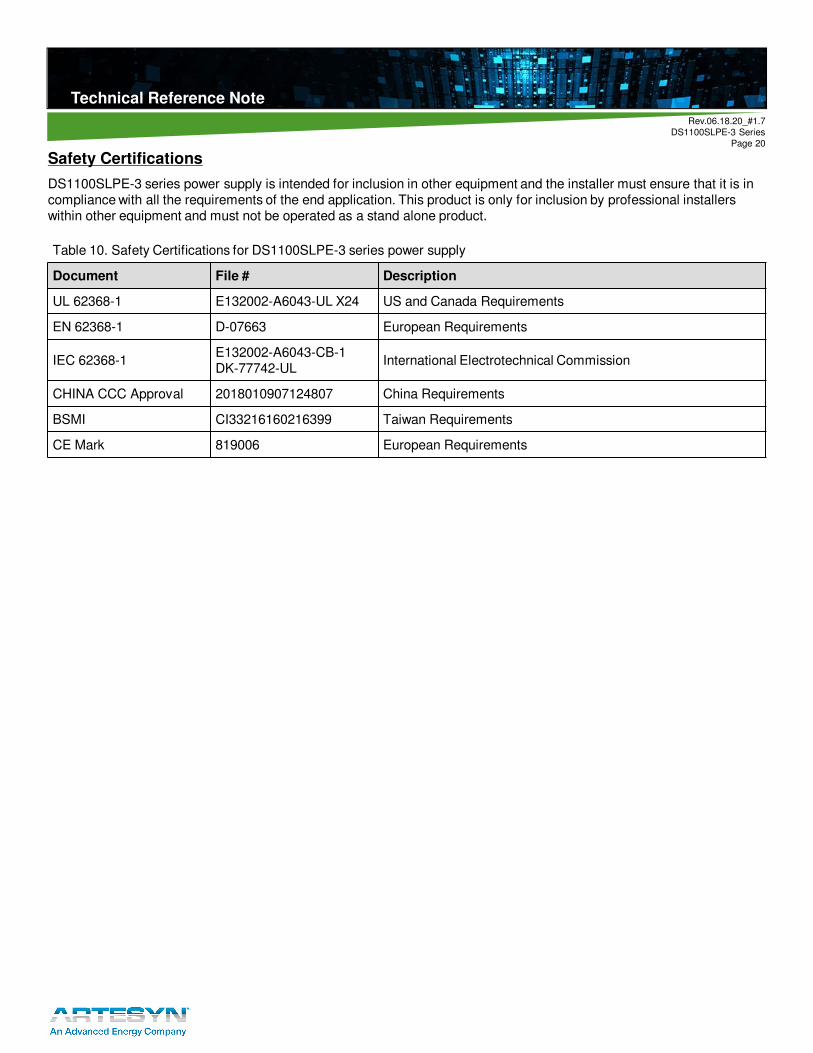
Safety Certifications
DS1100SLPE-3 series power supply is intended for inclusion in other equipment and the installer must ensure that it is in compliance with all the requirements of the end application. This product is only for inclusion by professional installers within other equipment and must not be operated as a stand alone product.
Table 10. Safety Certifications for DS1100SLPE-3 series power supply
Document File # Description
UL 62368-1 E132002-A6043-UL X24 US and Canada Requirements
EN 62368-1 D-07663 European Requirements
IEC 62368-1E132002-A6043-CB-1 DK-77742-UL
International Electrotechnical Commission
CHINA CCC Approval 2018010907124807 China Requirements
BSMI CI33216160216399 Taiwan Requirements
CE Mark 819006 European Requirements
Technical Reference NoteTechnical Reference Note
Rev.06.18.20_#1.7DS1100SLPE-3 Series
Page 21
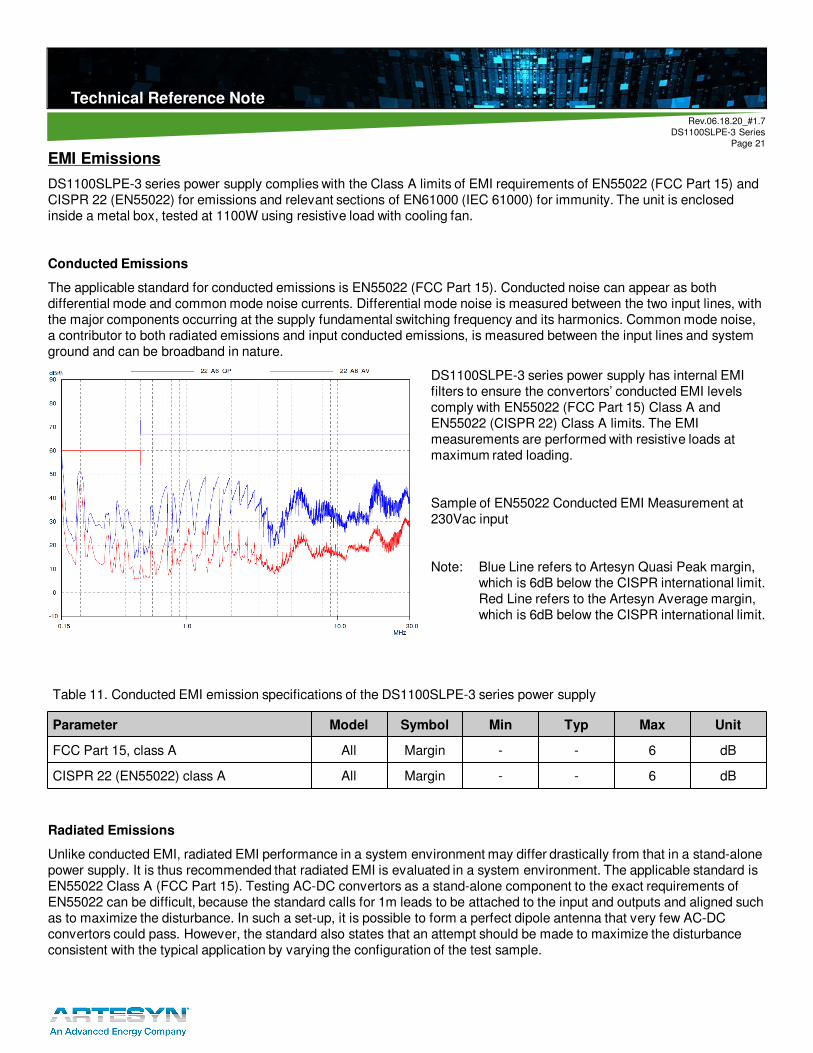
EMI Emissions
DS1100SLPE-3 series power supply complies with the Class A limits of EMI requirements of EN55022 (FCC Part 15) and CISPR 22 (EN55022) for emissions and relevant sections of EN61000 (IEC 61000) for immunity. The unit is enclosed inside a metal box, tested at 1100W using resistive load with cooling fan.
Conducted Emissions
The applicable standard for conducted emissions is EN55022 (FCC Part 15). Conducted noise can appear as both differential mode and common mode noise currents. Differential mode noise is measured between the two input lines, with the major components occurring at the supply fundamental switching frequency and its harmonics. Common mode noise, a contributor to both radiated emissions and input conducted emissions, is measured between the input lines and system ground and can be broadband in nature.
DS1100SLPE-3 series power supply has internal EMI filters to ensure the convertors’ conducted EMI levels comply with EN55022 (FCC Part 15) Class A and EN55022 (CISPR 22) Class A limits. The EMI measurements are performed with resistive loads at maximum rated loading.
Sample of EN55022 Conducted EMI Measurement at 230Vac input
Note: Blue Line refers to Artesyn Quasi Peak margin, which is 6dB below the CISPR international limit.Red Line refers to the Artesyn Average margin, which is 6dB below the CISPR international limit.
Radiated Emissions
Unlike conducted EMI, radiated EMI performance in a system environment may differ drastically from that in a stand-alone power supply. It is thus recommended that radiated EMI is evaluated in a system environment. The applicable standard is EN55022 Class A (FCC Part 15). Testing AC-DC convertors as a stand-alone component to the exact requirements of EN55022 can be difficult, because the standard calls for 1m leads to be attached to the input and outputs and aligned such as to maximize the disturbance. In such a set-up, it is possible to form a perfect dipole antenna that very few AC-DC convertors could pass. However, the standard also states that an attempt should be made to maximize the disturbance consistent with the typical application by varying the configuration of the test sample.
Table 11. Conducted EMI emission specifications of the DS1100SLPE-3 series power supply
Parameter Model Symbol Min Typ Max Unit
FCC Part 15, class A All Margin - - 6 dB
CISPR 22 (EN55022) class A All Margin - - 6 dB
Technical Reference NoteTechnical Reference Note
Rev.06.18.20_#1.7DS1100SLPE-3 Series
Page 22
Operating Temperature
DS1100SLPE-3 power supply can start and operate within stated specifications at an ambient temperature from -5OC to 55OC under all load conditions with internal fan. DS1100SLPE-3 series can provide derated output power 660W from 55OC up to 65OC ambient temperature max.
The DS1100SLPE-3-001 power supplies can start and operate within stated specifications at an ambient temperature from -5OC to 45OC under all load conditions with internal fan. DS1100SLPE-3-001 series can provide derated output power 660W from 45OC up to 55OC ambient temperature max.
Forced Air Cooling
DS1100SLPE-3 series power supply includes internal cooling fans as part of the power supply assembly to provide forced air-cooling to maintain and control temperature of devices and ambient temperature in the power supply to appropriate levels. The standard direction of airflow is from the DC connector end to the AC connector end of the power supply.
The cooling fan is a variable speed fan. In Standby mode power supply fan will operate at minimum speed to maintain component reliability at all load, line and ambient conditions. When 12V output is enabled, power supply fan will operate at minimum achievable fan speed. Power supply fan speed control algorithms will vary the speed so that the critical component temperatures do not exceed safe operating levels. Fans will be powered from voltage source inside the power supply and from system side voltage source.
The minimum airflow to cool the power supply is 9 CFM. The system backpressure may reduce the CFM through the power supply, so care must be taken to ensure that the minimum airflow is met while operating at 100% load.”
Power Derating
DS1100SLPE-3 & DS1100SLPE-3-001 total output power will be derated according to the table shown below.
Table 12. Power Derating
Model Notes Min Max AltitudeSystem Back
Pressure
DS1100SLPE-3
1100W load 0 OC 55 OC 6000 ft 0.8” H2O
660W load 0 OC 55 OC 10000 ft 1.2” H2O
660W load -5 OC 65 OC 6000 ft 1.2” H2O
DS1100SLPE-3-001
1100W load 0 OC 45 OC 6000 ft 0.8” H2O
660W load 0 OC 45 OC 10,000 ft 1.2” H2O
660W load -5 OC 55 OC 6,000 ft 1.2” H2O
Technical Reference NoteTechnical Reference Note
Rev.06.18.20_#1.7DS1100SLPE-3 Series
Page 23
Storage and Shipping Temperature
DS1100SLPE-3 series power supply can be stored or shipped at temperatures between -40OC to +85OC.
Altitude
DS1100SLPE-3 power supply operates within specifications at altitudes up to 6000 feet above sea level (ambient temperature derated to 55OC at 10,000 feet).
DS1100SLPE-3-001 power supply operates within specifications at altitudes up to 6000 feet above sea level (ambient temperature derated to 45OC at 10,000 feet).
The power supply will not be damaged when stored at altitudes of up to 50,000 feet above sea level.
Humidity
Operating: DS1100SLPE-3 series power supply operates with no degradation of performance while operating in range of 5% RH to 95%RH non-condensing.
Non-Operating: DS1100SLPE-3 series power supply operates with no degradation of performance while operating in range of 5%RH to 95%RH non-condensing.
Vibration
DS1100SLPE-3 series power supply passed the following random non-operational and non-operation vibration at levels according to the graph below:
DS1100SLPE-3 series power supply subjected to a swept sinusoidal vibration test at an acceleration amplitude of 0.5 g from 5 to 200 Hz and back to 5 Hz at 0.1 octave/minute, performed for 90 minutes for each of the three mutually perpendicular axes.
Technical Reference NoteTechnical Reference Note
Rev.06.18.20_#1.7DS1100SLPE-3 Series
Page 24
Shock
DS1100SLPE-3 series power supply passed the following shock specifications:
Non-Operating Half-Sine Shock
Operating Half-Sine Shock
All components within the power supply will be appropriately secured to prevent failure resulting from these tests. At the conclusion of any of the above referenced Shock/Vibration tests listed in this section of this document, the power supply will be powered up under maximum rated load and will perform within specification.
Acoustic
DS1100SLPE-3 series power supply noise level will not exceed 43dB when operated at 115Vac/230Vac, at 60% load, 40degC and 6,000ft. At worst case condition, the power supply noise shall not exceed 76dB.
Acceleration 30 G
Duration 18 mSec
Pulse Half-since shock
No. of Shock 3 time on all 6 faces
Acceleration 15 G
Duration 11 mSec
Pulse Half-since shock
No. of Shock 3 times on all 6 faces
Technical Reference NoteTechnical Reference Note
Rev.06.18.20_#1.7DS1100SLPE-3 Series
Page 25
Power and Control Signal Descriptions
AC Input Connector
This connector supplies the AC Mains to DS1100SLPE-3 series power supply.
Pin 1 - LPin 2 - NPin 3 - Earth Ground
Output Connector - Power Blades
These pins provide the main output for the DS1100SLPE-3. The + Main Output (VO) and the Main Output Return pins are the positive and negative rails, respectively, of the VO main output of the DS1100SLPE-3 power supply. The Main Output (VO) is electrically isolated from the power supply chassis ground at least 50V.
P1-P5 - +12V ReturnP6-P10 - 12V
Output Connector - Control Signals
DS1100SLPE-3 series power supply contains a 25 pins control signal header providing an analogue control interface, standby power and I2C interface signal connections.
Standby Output - (pins A1, B1, C1, D1, E1)
DS1100SLPE-3 series power supply provides a regulated 3.3V 3A auxiliary output voltage to power critical circuitry that must remain active regardless of the on/off status of the power supply’s main output. The Standby Output (VSB) voltage is available whenever a valid DC input voltage is applied to the unit.
A0, A1, A2 - (pins B3, D4, A3)
Please refer to “Communication Bus Descriptions” section.
SDA, SCL and PS_INTERRUPT_L - (pins C3, A4, C4)
Please refer to “Communication Bus Descriptions” section.
Main Output Remote Sense Return, Main Output Remote Sense - (pins D3, E3)
The main output of the DS1100SLPE-3 is equipped with a Remote Sensing capability that will compensate for a power path drop around the entire loop of 200 mV. This feature is implemented by connecting the Main Output Remote Sense (pin E3) and the Main Output Remote Sense Return (pin D3) to the positive and negative rails of the main output, respectively, at a location that is near to the load. This remote sense circuit will not raise the power supply’s output voltageto the OVP trip level. Main Output Remote Sense has no effect on the standby output (VSB).
In the event of a failure of the Remote Sense lines, the output voltage will revert to the internal sense so as to limit the output voltage to less than 105% of the nominal.
Technical Reference NoteTechnical Reference Note
Rev.06.18.20_#1.7DS1100SLPE-3 Series
Page 26
PSON_L - (pin B4)This signal input pin controls the normal turning ON and OFF of the Main Output of the DS1100SLPE-3 power supply. The power supply main output (VO) will be enabled when this signal is pulled low, below 0.8V. The power supply output (except VSB output) will be disabled when this input is driven higher than 2.0V, or open circuited. It’s recommended that to this pin is pulled up to 3.3VSB by a 5.1Kohm resistor and pulled down with a switch and 100pF decoupling capacitor to GND.
AC_OK - (pin E4)
Signal used to indicate the presence of DC input to the power supply. A logic level HIGH will indicate that the DC input to the power supply is within the operating range while a logic level LOW will indicate that DC input has been lost. This is an open collector/drain output. This pin is pulled high by a 10K ohm resistor connected to 3.3V inside the power supply. It is recommended that this pin is connected to a 200pF decoupling capacitor and pulled down by a 100K ohm resistor.
Power supply side Customer system side
Power supply side
INPUT_OK
100K
Rsys200pF
System GND
Customer system side
C
Enables/disables the main output at system side
IC201
Technical Reference NoteTechnical Reference Note
Rev.06.18.20_#1.7DS1100SLPE-3 Series
Page 27
PSKILL_L - (pin A5)
First break/Last Mate active HIGH signal which enables/disables the main output. When this signal is shorted to ground by the system, the 12V main output will be enabled. This signal will have to be pulled to ground at the system side with a 100 ohm resistor. A 100pF decoupling capacitor is also recommended.
ISHARE - (pin S7)
DS1100SLPE-3 series power supply supports active current sharing through a single wire connection between the power supplies. This input/output signal pin allows two or more power supplies to share the main output load current to increase the overall power capability or to operate the units in a N+N configuration for redundancy purposes.
All outputs of the DS1100SLPE-3 with ISHARE pins connected will share load current and the current share errors (CSE) is within 5.625A of each. If any power supply is hot swapped, no glitch will occur that violates the regulation limits of thepower supply defined in this specification. The current share loop should be activated when the output current exceed 7% of total load current.
The voltage of this signal is a linear slope from no load to full load. At 10% load of each power supply output when two supplies are running in parallel, the ISHARE voltage will be between 0.6V and 1.0V. At 50% load of each power supply output when two supplies are running in parallel, the ISHARE voltage will be between 3.85V and 4.15V. At 100% load of each power supply output when two supplies are running in parallel, the ISHARE voltage will be between 7.75V and 8.25V. The waveform for this signal will be provided to confirm stability during parallel mode operation.
Enables/disables the main output at system side
Rsys
0.1k
Power supply side Customer system side
100pFC
PSKILL_L
Technical Reference NoteTechnical Reference Note
Rev.06.18.20_#1.7DS1100SLPE-3 Series
Page 28
Power supply side
100pFRsys
100K ohm
System GND
Customer system side
PWOK - (pin C5)
Signal used to indicate that main output voltage is within regulation range. The PWOK signal will be driven HIGH (>2.0V) when the output voltage is valid and will be driven LOW (<0.8V) when the output falls below the under-voltage threshold. This signal also gives an advance warning when there is an impending power loss due to loss of DC input or system shutdown request.
This is an open collector/drain output. This pin is pulled high by a 10K ohm resistor connected to 3.3V inside the power supply. It is recommended that this pin be connected to a 100pF decoupling capacitor and pulled down by a 100K ohm resistor.
PS_PRESENT_L - (pin E5)
Signal used to indicate to the system that a power supply is inserted in the power bay. This pin is shorted to the Standby return via 220ohm resister in the power supply. Recommended pull-up resistor to 3.3VSB is 5.1K ohm. A 100pF decoupling capacitor is also recommended.
PWOK
IC201
Technical Reference NoteTechnical Reference Note
Rev.06.18.20_#1.7DS1100SLPE-3 Series
Page 29
Communication Bus Descriptions
I2C Bus Signals
DS1100SLPE-3 series power supply contains enhanced monitor and control functions implemented via the I2C bus. The DS1100SLPE-3 I2C functionality (PMBusTM and FRU data) can be accessed via the output connector control signals. The communication bus is powered either by the internal 3.3V supply or from an external power source connected to the Standby Output (i.e. accessing an unpowered power supply as long as the Standby Output of another power supply connected in parallel is on).
If units are connected in parallel or in redundant mode, the Standby Outputs must be connected together in the system. Otherwise, the I2C bus will not work properly when a unit is inserted into the system without the DC source connected.
Note: PMBusTM functionality can be accessed only when the PSU is powered-up.Guaranteed communication I2C speed is 100K Hz.
These input pins are the address lines A0 and A1 to indicate the slot position the power supply occupies in the power bay and define the power supply addresses for FRU data and PMBusTM data communication. This allows the system to assign different addresses for each power supply. During I2C communication between system and power supplies, the system will be the master and power supplies will be slave.
They are internally pulled up to internal 3.3V supply with a 10K resistor.
Note: A2 address line will be an optional address line. By default, the power supply address will ignore the A2 input and will relyexclusively on A0 and A1 logic levels. The address will begin at B0h and A0h. The default address of the power supply will be B6/B7 and A6/A7 when the address lines are left open. This ignores the logic level of A2.
SDA, SCL (I2C Data and Clock Signals) - (pins C3, A4)
I2C serial data and clock bus - these pins are internally pulled up to internal 3.3V supply with a 10K ohm resistor. These pins must be pulled-up by a 2.2K ohm resistor to 3.3V and a 200pF decoupling capacitor at the system side.
PS_INTERRUPT_L - (pin C4)
PS_INTERRUPT is used to send a signal to the system that a fault in the power supply occurred. This signal is normally logic level HIGH. It will go to a LOW logic level when a fault bit has been set in the power supply’s status register. This event can be triggered by faults such as OVP, OCP, OTP, and fan fault. The conditions wherein the signal goes back to high are: (1) DC recycle, (2) PSON recycle and (3) issuance of a CLEAR_FAULTS PMBus command. Recommended pull-up resistor to 3.3V VSB is 5.1K ohm. A 100pF decoupling capacitor is also recommended.
I2C Bus Communication Interval
The interval between two consecutive I2C communications to the power supply should be at least 15ms to ensure proper monitoring functionality.
I2C Bus Signal Integrity
The noise on the I2C bus (SDA, SCL lines) due to the power supply will be less than 300mV peak-to-peak. This noise measurement should be made with an oscilloscope bandwidth limited to 100MHz. Measurements should be make at the power supply output connector with 10K ohm resistors pulled up to Standby Output and 47pF ceramic capacitors to Standby Output Return.
Technical Reference NoteTechnical Reference Note
Rev.06.18.20_#1.7DS1100SLPE-3 Series
Page 30
I2C Bus Internal Implementation, Pull-ups and Bus Capacitances
I2C Bus - Recommended external pull-ups:
SystemBackplaneProcessor
SYSTEMBACKPLANE
POWER SUPPLY SIDESystem 3.3V (Internal Secondary Logic Supply
100K
10K
PSU MonitorFunction
PSU MicroControllerSDA SDA
SCL SCL
A1 A1
A0 A0
FRUDATA
EEPROM
GND
Interconnect
PS_INTERRUPT_L
Electrical and Interface specifications of I2C signals (referenced to Standby Output Return pin, unless otherwise indicated):
Parameter Condition Symbol Min Typ Max Unit
SDA, SCL internal pull-up resistor Rint - 10 - Kohm
DS1100SLPE-3 series power supply I2C communication bus will respond to logic levels as per below:
Logic High: 3.3V Nominal (Specs is 2.1V to 5.5V)**Logic Low: 500mV nominal (Specs is 800mV max)**** Note : Artesyn 73-769-001 I2C adapter was used.
Timings
Parameter SymbolStandard-Mode Specs
Actual UnitMin Max
SCL Clock Frequency fSCL 0 100 100 KHz
Hold time (repeated) START condition
tHD;STA 4.0 - 4.98 uSec
LOW period of SCL clock tLOW 4.7 - 4.95 uSec
HIGH period of SCL clock tHIGH 4.0 - 4.0 uSec
Setup time for repeated START condition
tSU;STA 4.7 - 4.8 uSec
Data hold time tHD;DAT 0 3.45 0.2 uSec
Data setup time tSU;DAT 250 - 4800 nSec
Rise time tr - 1000 SCL = 720 SDA = 740 nSec
Fall time tf - 300 SCL = 190 SDA = 210 nSec
Setup time for STOP condition tSU;STO 4.0 - 5.3 uSec
Bus free time between a STOP and START condition
tBUF 4.7 - 30.6 mSec
Technical Reference NoteTechnical Reference Note
Rev.06.18.20_#1.7DS1100SLPE-3 Series
Page 32
Device Addressing
DS1100SLPE-3 series power supply will respond to supported commands on the I2C bus that are addressed according to pins A1 and A0 pins of output connector.
Address pins are held HIGH by default via pulled up to internal 3.3V supply with a 2.2K resistor. To set the address as “0”, the corresponding address line should be pulled down to logic ground level. Below tables show the address of the power supply with A0 and A1 pins set to either “0” or “1”.
DS1100SLPE-3 series power supply can be used singly or in n + 1 (n = 1,2 or 3) configuration. The power supply
addressing, refers to the address of each power supply if it is used in N + 1 configuration. This will allow the system to assign different addresses for each PSU. During I2C communication between system and PSU, the system will be the master and the PSU will be slave. The address lines (A1 and A0) are pulled up to +3V3standby internally. To set the address as “low” the corresponding address should be pulled down to Ground (reference).
.
PSU SlotSlot ID Bits PMBusTM Address EEPROM (FRU) Address
A21 A1 A0 WRITE READ WRITE READ
1 0 0 0 0xB0 0xB1 0xA0 0xA1
2 0 0 1 0xB2 0xB3 0xA2 0xA3
3 0 1 0 0xB4 0xB5 0xA4 0xA5
4 0 1 1 0xB6 0xB7 0xA6 0xA7
5 1 0 0 0xB8 0xB9 0xA8 0xA9
6 1 0 1 0xBA 0xBB 0xAA 0xAB
7 1 1 0 0xBC 0xBD 0xAC 0xAD
8 1 1 1 0xBE 0xBF 0xAE 0xAF
Note 1 - A2 address line is an optional address line. By default, the power supply address will ignore the A2 input and will relyexclusively on A0 and A1 logic levels. The address will begin at B0h and A0h. The default address of the power supply are B6/B7 and A6/A7 when the address lines are left open. This ignores the logic level of A2.
Technical Reference NoteTechnical Reference Note
Rev.06.18.20_#1.7DS1100SLPE-3 Series
Page 33
Reporting Functions
The power supply will have enhanced monitor and control functions implemented via the I2C bus. This will use the SDA and SCL pins. The power supply monitor will operate as an I2C slave device. The accuracy of the report functions will be as follows:
Firmware Reporting And Monitoring
Output loading1 <10% 10 to 20% 20 to 100%
Input voltage ±5%
Input current2 ±1.0A fixed error ±10% ±5%
Input power3 30W fixed error up to 120W input power
±15% ±10%
Output voltage ±5% ±2%
Output current ±0.8A fixed error ±5% ±2%
Output power 12.0W fixed error ±15% ±5%
Temperature ±5 degC on the operating range
Fan speed Actual ±250 RPM
PMBus Yes
Remote ON/OFF Yes
Note 1 - Accuracy percentages are applicable for when the input voltage is at 115Vac/230Vac and the operating
temperature is at 25degC.
Note 2 - When the input current is less than 0.4A, the input current and input power can report a zero.
Note 3 - A power supply without input power in redundant mode operation will report zero input parameters.
Technical Reference NoteTechnical Reference Note
Rev.06.18.20_#1.7DS1100SLPE-3 Series
Page 34
I2C Clock Synchronization
The DS1100SLPE-3 power supply might apply clock stretching. An addressed slave power supply may hold the clock line (SCL) low after receiving (or sending) a byte, indicating that it is not yet ready to process more data.
The system master that is communicating with the power supply will attempt to raise the clock to transfer the next bit, but must verify that the clock line was actually raised. If the power supply is clock stretching, the clock line will still be low (because the connections are open-drain).
The maximum time out condition for clock stretching for DS1100SLPE-3 is 25 millisecond.
The power supply has a command completion timeout of 100 millisecond. That is, a single transaction (from START to STOP condition) must be finished within 100 millisecond.
Technical Reference NoteTechnical Reference Note
Rev.06.18.20_#1.7DS1100SLPE-3 Series
Page 35
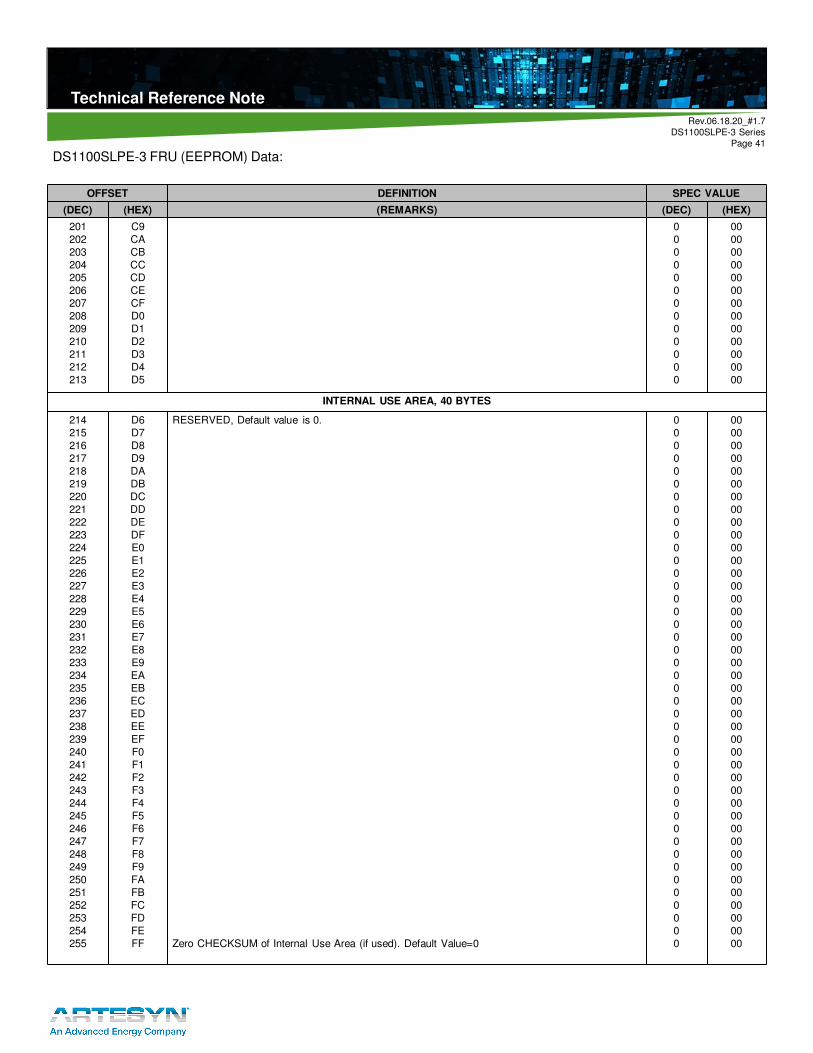
DS1100SLPE-3 FRU (EEPROM) Data:
OFFSET DEFINITION SPEC VALUE
(DEC) (HEX) (REMARKS) (DEC) (HEX)
COMMON HEADER, 8 BYTES
0 00 FORMAT VERSION NUMBER (Common Header) 7:4 - Reserved, write as 0000b3:0 - Format Version Number = 1h for this specification
1 01
1 01 INTERNAL USE AREA OFFSET 27 1B
2 02 CHASSIS INFO AREA OFFSET 1 01
3 03 BOARD INFO AREA OFFSET 0 00
4 04 PRODUCT INFO AREA OFFSET 5 05
5 05 MULTI RECORD AREA OFFSET 13 0D
6 06 PAD (reserved) Default value is 0. 0 00
7 07 ZERO CHECK SUM (256 - (Sum of bytes 0 to 6)) 209 D1
CHASSIS INFO AREA( 32 BYTES)
This area will be filled by the Mfg. Diag. or by the OS if used.
8 08 FORMAT VERSION NUMBER (Default value is 0.)7:4 - Reserved, write as 0000b3:0 - Format Version Number = 1h for this specification
1 01
9 09 CHASSIS INFO AREA LENGTH in multiple of 8 bytes 4 04
10 0A CHASSIS TYPE (Default value is 0.) 0 00
11 0BCHASSIS PART NUMBER Type/Length CAh (if used)Type = "ASCII+LATIN1" = (11)b Length = 10 Bytes = (001010)b 202 CA
12131415161718192021
0C0D0E0F101112131415
CHASSIS PART NUMBER BYTES (Default value is 0.) 0000000000
“Z” for "Zhongshan" In Decimal = 090 In Hex = 5AH 90 5A
102 66 End Tag 193 C1
103104105
676869
PAD (reserved) (Default value is 0.)
ZERO CHECK SUM(256-(sum of bytes 40 to 104 )) Per UnitZero Check Sum :Should follow check sum calculation as per IPMI v1.1
00
xxx
0000
xx
Technical Reference NoteTechnical Reference Note
Rev.06.18.20_#1.7DS1100SLPE-3 Series
Page 38
DS1100SLPE-3 FRU (EEPROM) Data:
OFFSET DEFINITION SPEC VALUE
(DEC) (HEX) (REMARKS) (DEC) (HEX)
Multi Record Area, 88 Bytes
106107108109
110
6A6B6C6D
6E
Power Supply Record Header
Record type = 00 for Power supplyEnd of List /Record Format Version NumberRecord Length of Power Supply RecordRecord CHECKSUM of Power Supply Record (Zero CHECKSUM)(256-(sum of bytes 111 to 130)Header CHECKSUM of Power Supply Record Header (Zero CHECKSUM)(256-(sum of bytes 106 to 109)
Low End Input Voltage Range 1(10mV), (90V / 10mV) 9000 = 2328H
2 Bytes SequenceIn Decimal = 40, In Hex = 28HIn Decimal = 35, In Hex = 23H
4035
2823
119120
7778
High End Input Voltage Range 1(10mV), (264V/10mV) 26400= 6720H
2 Bytes SequenceIn Decimal = 32, In Hex = 20HIn Decimal = 103, In Hex = 67H
32103
2067
121 79 Low End Input Frequency Range, 47Hz = 2FH 47 2F
122 7A Low End Input Frequency Range, 63Hz = 3FH 63 3F
123 7B AC Dropout Tolerance in mS, 10mS=0AH 10 0A
124 7C Binary Flags, 1 indicates function supported and a 0 indicates function not supported.
Bits 7-5: RESERVED, WRITE AS 000BBit 4: Tachometer Pulses Per Rotation / Predictive Fail Polarity BIT= 1Bit 3: Hot Swap / Redundancy Support BIT = 1Bit 2: Auto switch Support BIT = 1Bit 1: Power Factor Correction Support BIT = 1Bit 0: Predictive Fail Support BIT = 0
30 1E
125126
7D7E
Peak Wattage Capacity and Holdup Time
For DS1100SLPE-3 = DS1100SLPE3-001 = 14mS = 0EH;In Decimal = 14, In Hex = 0EHIn Decimal = 0, In Hex = 00H
130 82Predictive Fail Tachometer Lower Threshold, Not Applicable.Predictive Failure is not Supported. 0 00
Technical Reference NoteTechnical Reference Note
Rev.06.18.20_#1.7DS1100SLPE-3 Series
Page 39
DS1100SLPE-3 FRU (EEPROM) Data:
OFFSET DEFINITION SPEC VALUE
(DEC) (HEX) (REMARKS) (DEC) (HEX)
12V DC OUTPUT RECORD HEADER
131132133
134
135
838485
86
87
Record type = 01 for DC Output RecordEnd of List /Record Format Version Number for 12V DC Output RecordRecord Length of 12V DC Output RecordRecord CHECKSUM of 12V DC Output Record (Zero CHECKSUM)(256-(sum of bytes 136 to 148)Header CHECKSUM of 12V DC Output Record Header (Zero CHECKSUM)(256-(sum of bytes 131 to 134)
12 13
228
12
01020D
E4
0C
12V OUTPUT RECORD
136 88
Output Information, 001 = 01H
Bit 7: Standby Information = 0BBits 6-4: Reserved, Write as 000BBits 3-0: Output Number 1 = 001B 1 01
137138
898A
Nominal Voltage (10mV), (12V / 10mV) 1200 = 04B0H
2 Bytes SequenceIn Decimal: 176, In Hex: B0HIn Decimal: 4, In Hex: 04H
1764
B004
139140
8B8C
Maximum Negative Voltage Deviation (10mV), 1164 = 048CH
2 Bytes SequenceIn Decimal: 140, In Hex: 8CHIn Decimal: 4, In Hex: 04H
1404
8C04
141142
8D8E
Maximum Positive Voltage Deviation (10mV), 1236 =04D4H
2 Bytes SequenceIn Decimal: 212, In Hex: D4HIn Decimal: 4, In Hex: 04H
2124
D404
143144
8F90
Ripple and Noise pk-pk (mV), 180 = B4H2 Bytes SequenceIn Decimal: 180, In Hex: B4HIn Decimal: 0, In Hex: 00H
1800
B400
145146
9192
Minimum Current Draw (10mA), (0A / 10mA) 10 = 0000H2 Bytes SequenceIn Decimal: 0, In Hex: 00HIn Decimal: 0, In Hex: 00H
00
0000
147148
9394
Maximum Current Draw (10mA),
2 Bytes Sequence9000*10mA =2328H For DS1100SLPE-39000*10mA = 2328h For DS1100SLPE-3-001
4035
2823
VSB OUTPUT RECORD HEADER
149150151152
153
95969798
99
Record type = 01 for DC Output RecordEnd of List /Record Format Version Number for 3V3SB Output RecordRecord Length of 3V3SB Output RecordRecord CHECKSUM of 3V3SB Output Record (Zero CHECKSUM)(256-(sum of bytes 154 to 166)Header CHECKSUM of 3V3SB Output Record Header (Zero CHECKSUM)(256-(sum of bytes 149 to 152)
121367
173
01020D43
AD
VSB OUTPUT RECORD
154 9A Output Information, 002 = 02H
Bit 7: Standby Information = 1BBits 6-4: Reserved, Write as 000BBits 3-0: Output Number 1 = 0010B
130 82
155156
9B9C
Nominal Voltage (10mV), (3.3V / 10mV) 330 = 014AH
2 Bytes SequenceIn Decimal: 74, In Hex: 4AHIn Decimal: 1, In Hex: 01H
741
4A01
Technical Reference NoteTechnical Reference Note
Rev.06.18.20_#1.7DS1100SLPE-3 Series
Page 40DS1100SLPE-3 FRU (EEPROM) Data:
OFFSET DEFINITION SPEC VALUE
(DEC) (HEX) (REMARKS) (DEC) (HEX)
157158
9D9E
Maximum Negative Voltage Deviation (10mV), 314 = 013AH
2 Bytes SequenceIn Decimal: 58, In Hex: 3AHIn Decimal: 1, In Hex: 01H
581
3A01
159160
9FA0
Maximum Positive Voltage Deviation (10mV), 346 =015AH
2 Bytes SequenceIn Decimal: 212, In Hex: D4HIn Decimal: 4, In Hex: 04H
901
5A01
161162
A1A2
Ripple and Noise pk-pk (mV), 45 = 2DH2 Bytes SequenceIn Decimal: 45, In Hex: 2DHIn Decimal: 0, In Hex: 00H
450
2D00
163164
A3A4
Minimum Current Draw (10mA), (0A / 10mA) 10 = 00H2 Bytes SequenceIn Decimal: 0, In Hex: 00HIn Decimal: 0, In Hex: 00H
00
0000
165166
A5A6
Maximum Current Draw (4A), (3.0A / 10mA) 300 = 012CH
2 Bytes SequenceIn Decimal: 44, In Hex: 2CHIn Decimal: 1, In Hex: 01H
441
2C01
OEM RECORD HEADER
167168169170
171
A7A8A9AA
AB
Record type = C0H for OEM RecordEnd of List /Record Format Version Number for 3.3Vsb output RecordRecord Length of OEM RecordRecord CHECKSUM of OEM Record (Zero CHECKSUM)(256-(sum of bytes 172 to 213 )Header CHECKSUM of OEM Record Header (Zero CHECKSUM)(256-(sum of bytes 167 to 170 )
Manufacturer ID (3 bytes, Default is 0)RESERVEDRESERVEDRESERVEDRESERVEDRESERVEDRESERVEDRESERVEDRESERVEDRESERVEDRESERVEDRESERVEDRESERVEDPAD (reserved), Default value is 0.
40h - Disables write except 10h, 01h, and 00h commends
80h - Disable write except 0x00h
To save changes on the USER PMBusTM Table:
Use send byte command: 15h STORE_USER_ALL
To save changes on the DEFAULT PMBusTM Table:
Use send byte command: 11h STORE_DEFAULT_ALL
Wait for 5 seconds, turn-off the PSU, wait for another 5 seconds before turning it on.
Voltmeter
DS1100SLPE-3I2C Master I2C Adaptor E-Load
AC Source
Technical Reference NoteTechnical Reference Note
Rev.06.18.20_#1.7DS1100SLPE-3 Series
Page 43
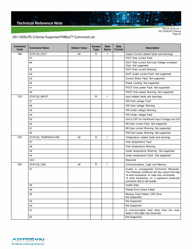
DS1100SLPE-3 Series Support PMBusTM Command List
The DS1100SLPE-3 is compliant with the industry standard PMBusTM protocol for monitoring and control of the power supply via the I2C interface port.
DS1100SLPE-3 Series Supported PMBusTM Command List:
Command
CodeCommand Name Default Value
Access
Type
Data
Bytes
Data
FormatDescription
00h Page 00 R 1
01h OPERATION 80 R/W 1 Used to Turn the unit ON/OFF in conjunction with the input CONTROL pin. It is also used to set output to upper or lower Margin Voltages. Valid input: 80h, 40h
02h ON_OFF_CONFIG 1D R 1 Configures the combination of CONTROL pin and serial communication commands needed to turn the Unit ON/OFF.
b7:5 00 Reserved
b4 - Enable CONTROL pin and Serial communication control.
1 1 - Unit powers up as dictated by CONTROL pin and OPERATION command (b3:0)
b3 - Serial communication Control
1 1 - Enables Serial communication ON/OFF portion of OPERATION command. Requires CONTROL pin to be asserted for the unit to start and energize the output.
b2 - Sets how the unit responds to CONTROL pin
1 1 - Unit requires CONTROL pin to be asserted to start the unit.
b1 - CONTROL pin polarity 0 0 - Active Low (Pull Low to start the unit)
b0 - CONTROL pin Action 0 0 - Use programmed turn ON/OFF delay
03h CLEAR_FAULTS S 0
10h WRITE_PROTECT 80 R/W 1 Used to Control Writing to the PMBus Device.
19h CAPABILITY 90 R 1Provides a way for the hosts system to determine some key capabilities of a PMBusdevice.
1Ah QUERY BW/BR 1/1 Varies
20h VOUT_MODE 17 R 1Specifies the mode and parameters of Output Voltage related Data Formats
21h VOUT_COMMAND 1800 R/W 2 Linear
Sets the Output Voltage Reference
Vout command sends discreet value to change
or trim output voltage. Valid range is 11.4 to 12.6V.
24h VOUT_MAX 1933 R 2 Linear Read Only (12.6V)
31h POUT_MAX 0A71 R 2/5 Default : 1250W
35h VIN_ON 0058 R 2 LinearSets the value of input, in volts, at which the unit should start. ACGOOD 88Vdc
36h VIN_OFF 004F R 2 LinearSets the value of input, in volts, at which the unit should stop power conversion. ACBAD 79Vac
Technical Reference NoteTechnical Reference Note
Rev.06.18.20_#1.7DS1100SLPE-3 Series
Page 44
DS1100SLPE-3 Series Supported PMBusTM Command List:
Command
CodeCommand Name Default Value
Access
Type
Data
Bytes
Data
FormatDescription
3Ah
FAN_ CONFIG_1_2 90 R 1 Read only to reflect setting of Fans
b7 11 - Fan is installed in position 10 - No Fan is installed in position 1
b6 01 - Fan is commanded in RPM0 - Fan is commanded in DC
b5:4 01
00 - 1 pulse per revolution01 - 2 pulses per revolution10 - 3 pulses per revolution11 - 4 pulses per revolution
b3 01 - Fan is installed in position 20 - No Fan is installed in position 2
b2 01 - Fan is commanded in RPM0 - Fan is commanded in DC
b1:0 00
00 - 1 pulse per revolution01 - 2 pulses per revolution10 - 3 pulses per revolution11 - 4 pulses per revolution
3Bh FAN_COMMAND_1 0000 R/W 2 Linear
Adjusts the operation of the Fans. The device may override the command, if it requires higher value, to maintain proper device temperature.
Default: 0%. Valid Range: 0- 100%.
40h VOUT_OV_FAULT_LIMIT 1A66 R/W 2 Linear Sets Output Over voltage threshold. (13.2V) Valid Range: 13.2V to 14.5V
41h VOUT_OV_FAULT_RESPONSE 80 R 1 Unit Latches OFF. Resets on PSON or CONTROL pin recycle or DC recycle.
42h VOUT_OV_WARN_LIMIT 1999 R/W 2 Linear Sets Over-voltage Warning threshold. (12.8V) Valid Range: 12.5 to 13.5V
43h VOUT_UV_WARN_LIMIT 1666 R/W 2 Linear Sets Under-voltage Warning threshold. (11.2V) Valid Range: 10.5 to 11.5V
44h VOUT_UV_FAULT_LIMIT 1333 R/W 2 Linear Sets Under-voltage Fault threshold. (9.6V) Valid Range: 9.5 to 11.5V
45h VOUT_UV_FAULT_RESPONSE 80 R 1 Turn PSU OFF. Delay time between restart attempts is 3 seconds.
46h IOUT_OC_FAULT_LIMIT EB60 R/W 2 Linear Sets the Over current threshold in Amps. (108A) Valid Range: 97 to 108A
47h IOUT_OC_FAULT_RESPONSE C0 R 1 OCP ride through. If OCP persists. Delay time between restart attempts is 2 seconds.
4Ah IOUT_OC_WARN_LIMIT EB20 R/W 2 Linear Sets the Over Current Warning threshold in Amps. (100A) Valid Range: 94 to 100A
4Fh OT_FAULT_LIMIT EB48 R/W 2 Linear Secondary ambient temperature Fault threshold, in degree C. (105degC)
50h OT_FAULT_RESPONSE F8 R 1 Turn PSU OFF and will retry indefinitely.Supported enable/disable of protection and recoverability.
51h OT_WARN_LIMIT EB20 R 2 Linear Secondary ambient temperature warning threshold, in degree C. Operating limit (100degC)
5Eh PWGOOD_ON 1766 R/W 2 Linear Sets the threshold by which the Power Good Default: 11.7V
5Fh PWGOOD_OFF 16CC R/W 2 Linear Sets the threshold by which the Power Good Default: 11.4V
61h TON_RISE 8BD7 R 2 Linear Sets the time (mS), for the output rises from 0 to regulation. Default=30ms
Technical Reference NoteTechnical Reference Note
Rev.06.18.20_#1.7DS1100SLPE-3 Series
Page 45
DS1100SLPE-3 Series Supported PMBusTM Command List:
Command
CodeCommand Name Default Value
Access
Type
Data
Bytes
Data
FormatDescription
64h TOFF_DELAY C280 R 2 Linear Sets the time (mS), from a stop condition (Power OFF) until the output starts to drop (converter OFF). Default: 2.5mS
78h STATUS_BYTE 00 R 1 Returns the summary of critical faults
b7 - BUSY - Not supported
b6 - OFF - Unit is OFF
b5 - VOUT_OV - Output over-voltage fault has occurred
b4 - IOUT_OC - Output over-current fault has occurred
b3 - VIN_UV - An input under--voltage fault has occurred
b2 - TEMPERATURE - A temperature fault or warning has occurred
b1 - CML - A communication, memory or logic fault has occurred.
b0 - NONE OF THE ABOVE - A Fault Warning not listed in bits[7:1] has occurred. Not supported
79h STATUS_WORD 0000 R 2 Summary of units Fault and warning status.
b15 - VOUT An output voltage fault or warning has occurred
b14 - IOUT/POUT An Output current or power fault or warning has occurred.
b13 - INPUT An input voltage, current or power fault or warning as occurred.
b12 - MFR A manufacturer specific fault or warning has occurred. Not supported
b11 - PWOK# The PWOK signal is de-asserted
b10 - FANS A fan or airflow fault or warning has occurred.
b9 - OTHER Not supported
b8 - UKNOWN Not supported
b7 - BUSY A fault was declared because the device was busy and unable to respond. Not supported
b6 - OFF Unit is OFF
b5 - VOUT_OV Output over-voltage fault has occurred
b4 - IOUT_OC Output over-current fault has occurred
b3 - VIN_UV An input under-voltage fault has occurred
b2 - TEMPERATURE A temperature fault or warning has occurred
b1 - CML A communication, memory or logic fault has occurred.
b0 - NONE_OF_THE_ABOVE A fault or warning not listed in bits[7:1] of this byte has occurred. Not supported
7Ah STATUS_VOUT 00 R 1 Output voltage related faults and warnings
b7 VOUT Over--voltage Fault
b6 VOUT Over-voltage warning
b5 VOUT Under-voltage Warning
b4 VOUT Under-voltage Fault
b3 VOUT_MAX Warning, an attempt has been made to set output to a value higher that the highest permissible voltage. Not supported
b2 TON_MAX_FAULT. Not supported
b1 TOFF_MAX Warning. Not supported
b0 Not supported.
Technical Reference NoteTechnical Reference Note
Rev.06.18.20_#1.7DS1100SLPE-3 Series
Page 46
DS1100SLPE-3 Series Supported PMBusTM Command List:
Command
CodeCommand Name Default Value
Access
Type
Data
Bytes
Data
FormatDescription
7Bh STATUS_IOUT 00 R 1 Output Current related faults and warnings
b7 IOUT Over current Fault
b6 IOUT Over current And Low Voltage shutdownFault. Not supported
b5 IOUT Over current Warning
b4 IOUT Under current Fault. Not supported
b3 Current Share Fault. Not supported
b2 Power Limiting. Not supported
b1 POUT Over power Fault. Not supported
b0 POUT Over power Warning. Not supported
7Ch STATUS_INPUT R 1 Input related faults and warnings
b7 VIN Over voltage Fault
b6 VIN Over voltage Warning
b5 VIN Under voltage Warning
b4 VIN Under voltage Fault
b3 Unit is OFF for insufficient Input Voltage (not UV)
b2 IIN Over current Fault. Not supported
b1 IIN Over current Warning. Not supported
b0 PIN Over power Warning. Not supported
7Dh STATUS_TEMPERATURE 00 R 1 Temperature related faults and warnings
b7 Over temperature Fault
b6 Over temperature Warning
b5 Under temperature Warning . Not supported
b4 Under temperature Fault . Not supported
b3:0 Reserved
7Eh STATUS_CML 00 R 1 Communications, Logic and Memory
b7 Invalid or unsupported Command Received.The following conditions will also assert this flag:-A write transaction on read only commands.-A write transaction on a password protectedcommand that is still locked .
b6 Invalid Data
b5 Packet Error Check Failed
b4 Memory Fault Detect, CRC ErrorNot Supported
b3 Not Supported
b2 Not Supported
b1 A communication fault other than the oneslisted in this table has Occurred.
b0 Not Supported
Technical Reference NoteTechnical Reference Note
Rev.06.18.20_#1.7DS1100SLPE-3 Series
Page 47
DS1100SLPE-3 Series Supported PMBusTM Command List:
Command
CodeCommand Name Default Value
Access
Type
Data
Bytes
Data
Format
Description
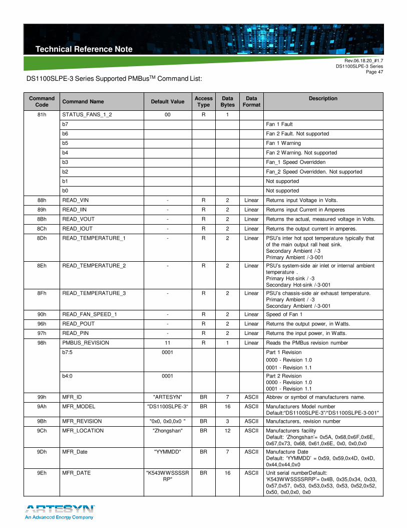
81h STATUS_FANS_1_2 00 R 1
b7 Fan 1 Fault
b6 Fan 2 Fault. Not supported
b5 Fan 1 Warning
b4 Fan 2 Warning. Not supported
b3 Fan_1 Speed Overridden
b2 Fan_2 Speed Overridden. Not supported
b1 Not supported
b0 Not supported
88h READ_VIN - R 2 Linear Returns input Voltage in Volts.
89h READ_IIN - R 2 Linear Returns input Current in Amperes
8Bh READ_VOUT - R 2 Linear Returns the actual, measured voltage in Volts.
8Ch READ_IOUT - R 2 Linear Returns the output current in amperes.
8Dh READ_TEMPERATURE_1 - R 2 Linear PSU’s inter hot spot temperature typically that of the main output rall heat sink. Secondary Ambient /-3 Primary Ambient /-3-001
8Eh READ_TEMPERATURE_2 - R 2 Linear PSU’s system-side air inlet or internal ambienttemperature . Primary Hot-sink / -3 Secondary Hot-sink /-3-001
8Fh READ_TEMPERATURE_3 - R 2 Linear PSU’s chassis-side air exhaust temperature. Primary Ambient / -3 Secondary Ambient /-3-001
90h READ_FAN_SPEED_1 - R 2 Linear Speed of Fan 1
96h READ_POUT - R 2 Linear Returns the output power, in Watts.
97h READ_PIN - R 2 Linear Returns the input power, in Watts.
98h PMBUS_REVISION 11 R 1 Linear Reads the PMBus revision number
D2h FAN_SPEED_MIN 2177 R 2 Linear Minimum Fan Speed (6000 RPM)
D3h FAN_SPEED_MAX 3168 R 2 Linear Maximum Fan Speed (23000 RPM)
E0h FW_PRI_VERSION BR 8 ASCII
E1h FW_SEC_VERSION BR 8 ASCII
F5h ISP_UNLOCK_CODE BW 4 ASCII 00h,00h,00h,00h
F6h ISP_CTRL_CMD W 1
F7h ISP_STATUS_BYTE R 1
F9h ISP_FLASH_DATA. BR/W 16
Technical Reference NoteTechnical Reference Note
Rev.06.18.20_#1.7DS1100SLPE-3 Series
Page 49
Application Notes
Redundancy / Fault Tolerance
The DS1100SLPE-3 series power supplies must be able to current share with 2(1+1) up to 6(3+3) power supplies in parallel and operate in a hot swap/redundant N+N configuration where N=1, 2, or 3. The 3.3V VSB outputs of the power supplies are connected together in the system so that a failure or hot swap of a redundant power supply does not cause these outputs to go out of regulation in the system.
All power supply outputs will be designed for redundant mode operation. No internal failure in any power supply in this configuration should cause the bus voltage to fall below the regulation limits specified. All output voltages should stay within the regulation limits during cold swapping or hot swapping operation.
Vo Or-ing
+Remote Sense
ISHARE
-Remote Sense
Vo Return
LOAD
Vo Or-ing
+Remote Sense
ISHARE
-Remote Sense
Vo Return
DS1100SLPE-3 DS1100SLPE-3
Technical Reference NoteTechnical Reference Note
Rev.06.18.20_#1.7DS1100SLPE-3 Series
Page 50
Current Sharing
The DS1100SLPE-3 series’ main output VO is equipped with current sharing capability. Single wire master-slave forced current share will be employed in this power supply. When two or more power supplies are connected and operating in parallel, the sharing accuracy between units must be within the limits specified in the table below.
The current sharing function may start when the total system load has reached 7% of the power supply rating. The power supply should be tested to support up to 6 units in parallel, with each power supply delivering 100% load. The current share signal, Imon, is a DC signal that represents the load current that a power supply is providing. This voltage will increase proportionately with the output load and will be represented by 8*Iout/Imax. The Ishare voltage should be within the voltage range specified below. It should be capable of sinking 0.4mA and sourcing 4mA. The waveform for this signal will be provided to confirm stability during parallel mode operation.
The current share signal may be disabled by shorting this pin to ground. The main output voltage should stay within regulation limits in this condition.
Table 13. Current Sharing Accuracy
Load (per power supply unit) Max Difference between PSUs
20%-100% 5.625A
<20% 5.625A
Table 14. Imon Signal Accuracy
Load (per power supply unit) Min Typ Max
100% 7.75 8 8.25
50% 3.85 4 4.15
10% 0.6 0.8 1.0
Technical Reference NoteTechnical Reference Note
Rev.06.18.20_#1.7DS1100SLPE-3 Series
Page 51
Output Ripple and Noise Measurement
The setup outlined in the diagram below has been used for output voltage ripple and noise measurements on the DS1100SLPE-3 Series. When measuring output ripple and noise, a scope jack in parallel with a 0.1uF ceramic chip capacitor, and a 10uF aluminum electrolytic capacitor should be used. Oscilloscope should be set to 20MHz bandwidth for this measurement.
1.1 05.04.2017Update the SCL/SDA internal pull up resistorUpdate the PWOK and ACOK internal pull up resistorUpdate the -6dB as typical rather than minimum.
K. Wang
1.2 07.05.2017Updated Table 3 Dynamic load and total range; added note on no load operation; updated standby ripple; added AC Input Sag and Surge
K. Zou
1.3 12.03.2017 Add minimum airflow definition in page 22. B. Wang
1.4 09.04.2018 Update Isolation Voltage according to CB report K. Zou
1.5 12.27.20181.Update the parallel number to 62.Command list 31h, 51h,64h
K. Wang
1.6 07.12.2019 Update the 40h valid range to 13.2 to 14.5V K. Wang
1.7 06.18.2020 Update safety 60950 to 62368 K. Zou