Page 1
A. Ostmann, T. Braun, L. Boettcher, R. Aschenbrenner and K.-D. Lang
Fraunhofer IZM, Berlin
Gustav-Meyer-Allee 25, 13355 Berlin, Germany
email: [email protected]
Panel Level Embedding for
Power and Sensor Applications
Page 2
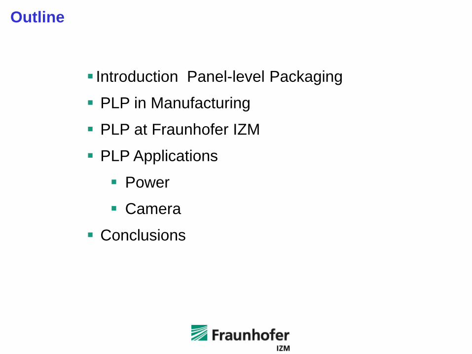
Introduction Panel-level Packaging
PLP in Manufacturing
PLP at Fraunhofer IZM
PLP Applications
Power
Camera
Conclusions
Outline
Page 3
Today's Packaging
Leadframe Packaging Strip Packaging Wafer-level Packaging
Fan-out Wafer-level Packaging
Need for further cost reduction
Increase of production format size
Page 4
source Yole
Evolution of FO WLP towards Panel-Level Packaging (PLP)
Page 5
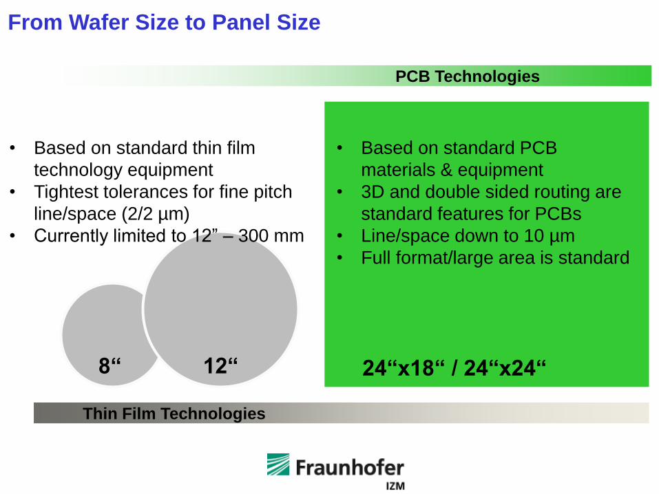
From Wafer Size to Panel Size
24“x18“ / 24“x24“ 12“ 8“
• Based on standard PCB
materials & equipment
• 3D and double sided routing are
standard features for PCBs
• Line/space down to 10 µm
• Full format/large area is standard
• Based on standard thin film
technology equipment
• Tightest tolerances for fine pitch
line/space (2/2 µm)
• Currently limited to 12” – 300 mm
Thin Film Technologies
PCB Technologies
Page 6
Panel-Level Packaging - PLP
Definition:
Throughout manufacturing of packages on large formats
Features
• Lead-less package (BGA, QFN, LGA)
• embedded components (active and passive )
• components on top
• high-density interconnects
• 3D capability
• rectangular or square production formats 18" - 24“ or larger
Page 7
Technologies for Panel-Level Packaging
Leadframe/
Strip Format
Wafer-Level
FO Wafer-Level
PCB Technology
Embedding
LCD Technology
Fusion of different technologies
equipment for
very large area
• polymer application
• metal sputtering
die attach
materials and processes
mold technology & materials / through mold vias
thin film materials / sputtering
advanced PCB processes & materials read for PLP
improvement resolution and accuracy for next Gen PLP
Page 8
Challenges for PLP Processes
Warpage ( Assembly, Manufacturability)
• heterogeneous materials and non-symmetric structures cause bow
• polymer materials with adapted CTE,& modulus and low shrink are required
• optimized layer sequence and design required
Accuracy/Resolution ( Miniaturization)
• improved optical recognition systems for placement equipment
• imaging with high depth of focus and high resolution
• local alignment LDI or stepper
Yield ( Cost)
• suited materials and components
• optimized processes
• production experience Learning Curve
Page 9
Panel-Level Packaging in
Manufacturing today
Page 10
Embedded Component Packaging (ECP)
courtesy AT&S
Page 11
courtesy AT&S
Embedded Component Packaging (ECP)
Page 12
courtesy AT&S/GaN Systems
Embedded Component Packaging (ECP)
Page 13
Semiconductor Embedded in Substrate (SESUB)
Page 14
J-Devices
source j-devices.co.jp
Page 15
Blade Package
SMD power packagea
embedded MOSFET / Driver
manufacturing on PCB format
Licensing and process transfer from Fraunhofer IZM
Page 16
Panel-Level Packaging at
Fraunhofer IZM
-
R&D for Future Products
Page 17
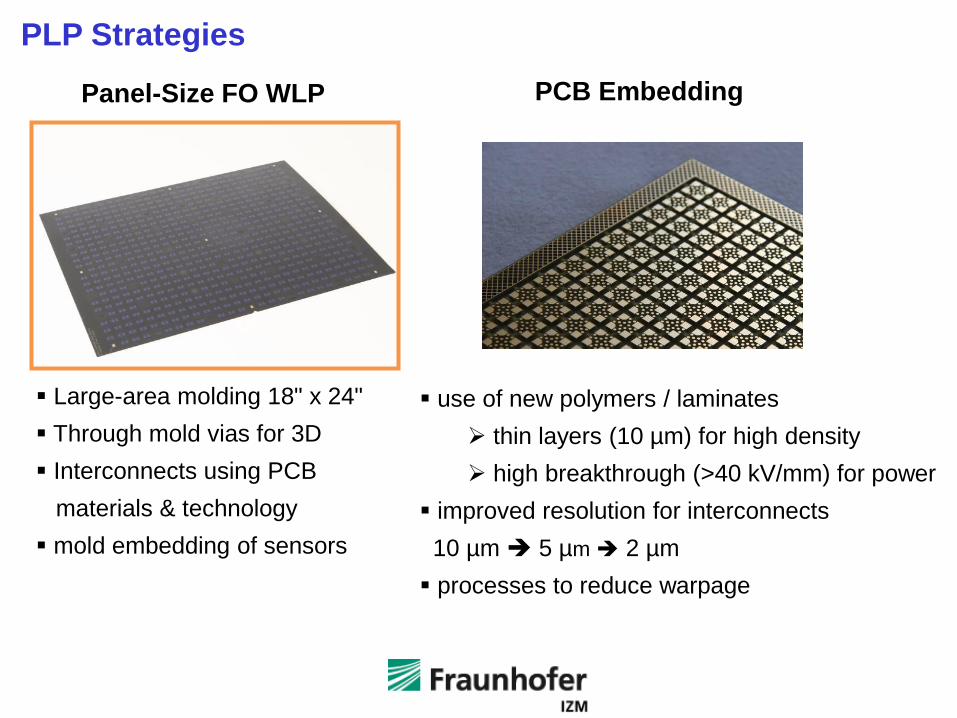
PLP Strategies
Panel-Size FO WLP PCB Embedding
Large-area molding 18" x 24"
Through mold vias for 3D
Interconnects using PCB
materials & technology
mold embedding of sensors
use of new polymers / laminates
thin layers (10 µm) for high density
high breakthrough (>40 kV/mm) for power
improved resolution for interconnects
10 µm 5 µm 2 µm
processes to reduce warpage
Page 18
Fraunhofer IZM Substrate Integration Line
Laser, drilling , lamination 400 m²
Lithography (LDI), sputtering 280 m²
galvanics, etching 100 m²
Assembly, molding, analytics 340 m²
Total area 1120 m²
High-end manufacturing equipment dedicated to customer-specific R&D
Complete 18" x 24 " PCB manufacturing & assembly line
40 scientist, engineers and technicians
with long-term experience in
advanced packaging
PCB laser, drilling & lamination lab
Page 19
Datacon evo/
ASM Siplace CA3
Mahr OMS 600/
IMPEX proX3
WL: Towa up to 8”
PL: APIC up to 18”x24”
incl. 12” WL (Q3 – 2014)
Lauffer/
Bürkle
Siemens Microbeam/
Schmoll Picodrill with
HYPER RAPID 50
Ramgraber automatic
plating line
Schmoll MX1 Orbotech
Paragon Ultra 200
Schmid
Fraunhofer IZM Substrate Integration Line
Page 20
Assembly of 5528 dies on large area
18”x 24” with 6500 dies/h speed
Mold embedding on large area
18”x 24” by sheet lamination
18”x 24” Panel-Level FO WLP
Fully electrical connected WL embedded package stack with TMV & 3D routing
Page 21
Panel Molding 18”x 24” – APIC Yamada
Equipment in Japan before shipment First molded panel 18" x 24 "
Large area compression molding: Wafer Level: 300 mm up to 450 mm possible Panel Level: 18” x 24” (456 x 610 mm²) Lamination Up and Running in Q4/2014
Page 22
Panel-Level Packaging for
Power Applications
Page 23
PCB Embedding Today – Power and Logic
The production of embedded packages is ramping up fast
Today 2013: 340 Mio., Forecast 2016; 1700 Mio. (source Yole)
Smart Phone Market
• DC/DC converters
• Power management units
• Connectivity module
Computer market
• MOSFET packages
• Driver MOS SiPs
PCB Embedding Technology is implemented or will come soon at
• PCB manufacturers
• Semiconductor manufacturers
• OSATS
Page 24
Embedding of power chips into Printed Circuit Board structures
cost saving by large area process PLP
Direct connection by Cu conductors / no bond wires
high reliability by direct Cu to chip interconnects
shielding capability
Completely planar conductors
multiple wiring layers possible
SMD assembly on top allows driver integration
top side cooling possible
very low parasitic effects
Power Chip Embedding - Features
Page 25
Power Chip Embedding – Manufacturing Process
backside contact by conductive die bond
conductive adhesive
soldering
sintering
very good thermal conductivity
die attach on thick Cu possible
compatible to standard Ag backside
conductive chip attach
embedding by lamination
via drilling top, through-via
Cu plating and structuring Ag sintered die bond
Page 26
Ultra Low Inductance Package for SiC
Full bus bar
structure using
PCB Process on
a DBC
DC capacitors
on the module
DC link current
measurement
included
Abb. 1: Explosionsansicht des Modulaufbaus
DC link
capacitors
DC+
Out
DC -
JFE
T Diode
DCB Gates
Current
measurement
Package sets new benchmark:
ultra-low DC-link inductance
Best Paper of PCIM 2013 Conference
Page 27
Switch off at 20 A:
Voltage slope 19 V/ns
current slope max. 4 A/ns
(50% to 90%)
Low overshot (appr. 10 V)
very little ringing
(frequency 240 MHz)
Ultra Low Inductance Package for SiC
0.8 nH DC-link inductance
Page 28
0,1
1
10
100
1000
10000
1 10 100 1000 10000
Reihe1
Reihe2
Reihe3
Power PLP – Production and R&D
Production
R&D Si
R&D SiC
R&D and Customer Projects
Voltage (V)
Cu
rren
t (A
)
1 MW
DC/DC converter SiPs
Blade Packages
Power PLP
products today
Page 29
Future Perspective – Power Electronics Packaging
wire-bonded power chips on DCB planar packages & module with embedded power chips
Traditional Power modules Planar Power Packaging
single module manufacturing large panel manufacturing
low inductance
high heat transfer
high integration level
high productivity
MOSFET MOSFET driver
IGBT IGBT
logic IC R C
Page 30
Panel-Level Packaging for
Sensor Applications
Page 31
MoMiCa – Modular Camera Module
Motivation
•to develop a miniaturized camera module
with integrated image processing
•using PCB PLP embedding
Potential Applications
traffic lane recognition face / gender recognition
Page 32
MoMiCa – Camera Module
Geometry
•16 x 16 x 3.6 mm³, weight 2 g w/o lens
PCB Layers
•2 + 8 + 1 construction
•8 layer core with stacked mircrovias
Embedded Components
•32 bit microcontroller with image sensor
interface (CogniVue CV2201 BGA 236 )
•256 Mbit Flash Memory (Macronix 8WSON
•MOSFET switch (IRF SOIC)
•USB ESD protection (NXP SOT457)
•5 DC/DC-converters (Murata)
•oscillator 24 MHz (NXP
•2 LEDs (0402)
•34 capacitors (0201, 0603)
•25 resistors (0201)
•3 inductors (0603)
Components on top
•3 MPixel Image Sensor
Omnivision 3642
•lens CMT746 + lens holder
•7 capacitors (0201)
•1 resistor (0201)
•1 inductor (0603)
•1 microswitch
Page 33
MoMiCa - Layer Sequence
SMD Bildsensor
2 Lagen Kern
Bauelemente
3 Build-up Lagen
2 Lagen Kern
3 Build-up Lagen
Bauelemente
Außenlage
Page 34
MoMiCa - PLP Manufacturing
assembled components on
bottom inner layer
assembled components on
top inner layer
• manufacturing on quarter format (12" x 9")
• 77 modules per panel (only partially with components)
• double-side component assembly on inner layer
• embedding by prepreg lamination
• assembly of image sensor on top
•t esting and programming on panel-level
Page 35
MoMiCa – Camera Module
Modular camera with integrated 32 bit image processor and memory
3 Mpixel image sensor
flash memory
DC/DC converter
capacitor
32 bit microcontroller
Page 36
Panel-level Packaging will gain a significant market share
There will be a fusion of different technologies
FO WLP will evolve towards large panels
PCB technology will evolve towards very high density
Power application are first in volume manufacturing
. . . it just started - take the opportunity !
Conclusions