8/7/2019 Parallel Power Flow ACDC Converter With High Input Power Factor and Tight Voltage Regulation http://slidepdf.com/reader/full/parallel-power-flow-acdc-converter-with-high-input-power-factor-and-tight-voltage 1/15 Parallel Power Flow AC/DC Converter with High Input power factor and Tight voltage Regulation Authorised By SANTOSH BHARADWAJ REDDY Email: [email protected]Engineeringpapers.blogspot.com More Papers and Presentations available on above site Abstract In this paper, A new parallel-connected single phase power factor correction (PFC) topology using flyback converter in parallel with forward converter is proposed to improve the input power factor with simultaneously output voltage regulation taking consideration of current harmonic norms. Paralleling of converter modules is a well-known technique that is often used in medium-power applications to achieve the desired output power by using smaller size of high frequency transformers and inductors. The proposed approach offers cost effective, compact and efficient AC-DC converter by the use of parallel power processing. Forward converter primarily regulates output voltage with fast dynamic response and it acts as master which processes 60% of the power. Flyback converter with AC/DC PFC stage regulates input current shaping and PFC, and processes the remaining 40% of the power as a slave. This paper presents a design example and circuit analysis for 300 W power supply. A parallel-connected interleaved structure offers smaller passive components, less loss even in continuous conduction inductor current mode, and reduced volt-ampere rating of DC/DC stage converter. MATLAB/SIMULINK is used f implementation and simulation results show the performance improvement. Index Terms Circuit analysis, PFC, Power Conversion. INTRODUCTION A number of power factor correction circuits have been developed recently [1]–[5]. Normally a boost converter is employed for PFC with DC/DC stage to improve performance or a flyback converter is used to reduce the cost. Although both boost converter and flyback converter are capable for PFC applications [6], [7], the main difficulty in two-stage scheme employing a PFC boost and a DC/DC converter is the high cost and lower efficiency. However, single-stage method using the simplest flyback converter is not able to tightly regulate the output voltage. Paralleling of converter power modules [8-9] is a well-known technique that is often used in high-power applications to achieve the desired output power with smaller size power transformers and inductors [10]. Since magnetics are critical components in power converters because generally they are the size-limiting factors in achieving high-density and/or low-profile power supplies, the design of magnetics becomes ev challenging for high-power applications that call for high
Transcript
8/7/2019 Parallel Power Flow ACDC Converter With High Input Power Factor and Tight Voltage Regulation
More Papers and Presentations available on above site
Abstract In this paper, A new parallel-connected single phase power factor correction
(PFC) topology using flyback converter in parallel with forward converter is proposed to
improve the input power factor with simultaneously output voltage regulation taking
consideration of current harmonic norms. Paralleling of converter modules is a well-known
technique that is often used in medium-power applications to achieve the desired output
power by using smaller size of high frequency transformers and inductors. The proposed
approach offers cost effective, compact and efficient AC-DC converter by the use of parallel
power processing. Forward converter primarily regulates output voltage with fast dynamic
response and it acts as master which processes 60% of the power. Flyback converter with
AC/DC PFC stage regulates input current shaping and PFC, and processes the remaining
40% of the power as a slave. This paper presents a design example and circuit analysis for
300 W power supply. A parallel-connected interleaved structure offers smaller passive
components, less loss even in continuous conduction inductor current mode, and reduced
volt-ampere rating of DC/DC stage converter. MATLAB/SIMULINK is used f
implementation and simulation results show the performance improvement.
Index Terms Circuit analysis, PFC, Power Conversion.
INTRODUCTION
A number of power factor correction circuits have been developed recently [1]–[5].Normally a boost converter is employed for PFC with DC/DC stage to improveperformance or a flyback converter is used to reduce the cost. Although both boostconverter and flyback converter are capable for PFC applications [6], [7], the maindifficulty in two-stage scheme employing a PFC boost and a DC/DC converter is the highcost and lower efficiency. However, single-stage method using the simplest flyback
converter is not able to tightly regulate the output voltage.Paralleling of converter power modules [8-9] is a well-known technique that is oftenused in high-power applications to achieve the desired output power with smaller sizepower transformers and inductors [10]. Since magnetics are critical components in power converters because generally they are the size-limiting factors in achieving high-densityand/or low-profile power supplies, the design of magnetics becomes evchallenging for high-power applications that call for high
power-density and low-profile packaging. Instead of designing large-size centralizedmagnetics that handle the entire power, low-power distributed high density low-profilemagnetics can be utilized to handle the high processing power, while only partial loadpower flow through each individual magnetics [10, 11].
In addition to physically distributing the magnetics and their power losses and thermalstresses, paralleling also distributes power losses and thermal stresses semiconductors due to a smaller power processed through the individual paralleled power stages. As a result, paralleling is a popular approach to eliminating "hot spots" in power supplies. In addition, the switching frequencies of paralleled, lower-power power stagesmay be higher than the switching frequencies of the corresponding single, high-power processing stages because lower-power, faster semiconductor switches can be used inimplementing the paralleled power stages. Consequently, paralleling offersopportunity to reduce the size of the magnetic components and to achieve a low-profiledesign for high power applications.
Without increasing the number of power stages and control-circuit components, the
transformer magnetics can be distributed by direct transformer paralleling. Not only thattransformer paralleling distributes the processed power in each magnetics components,but also their power losses and thermal stresses are distributed at the same time.However, current sharing among the paralleled transformers needs to be maintained toensure power balance.
In its basic form, the interleaving technique can be viewed as a variation of theparalleling technique, where the switching instants are phase-shifted within a switchingperiod [12]. By introducing an equal phase shift between the paralleled power stages, thetotal inductor current ripple of the power stage seen by the output filter capacitor islowered due to the ripple Cancellation effect [12].
This chapter discusses the paralleling techniques to achieve high-density, low-profiledesigns for relative high power applications. It analyzes and compares the current sharingin various implementations of transformer paralleling.
The goal of the proposed PFC scheme is to reduce the passive component size, toemploy lower rated semiconductor, and to improve total efficiency. Simulation resultsshow that the proposed topology is capable of offering good power factor correction andfast dynamic response.
PFC Cells
A. Two Stage PFC ApproachA two-stage scheme shown in Fig. 1 is mainly employed for the switching power
supplies since the boost stage can offer good input power factor with low total harmonicdistortion (THD) and regulate the dc-link voltage and the DC/DC stage is able to obtainfast output regulation without low frequency ripple due to the regulated dc-link voltage[13]. These two power conversion stages are controlled separately. However, two-stagescheme suffers from higher cost, complicated control, low-power density, and lower efficiency
B. SINGLE STAGE PFC APPROACH
8/7/2019 Parallel Power Flow ACDC Converter With High Input Power Factor and Tight Voltage Regulation
For low power applications, where cost is a dominant issue, a single-stage schemeusing the flyback converter [14] Fig. 2 is more attractive than a two-stage scheme due tothe following advantages.
Simplified power stage and control circuit (low parts count, low-cost
design).
Provides isolation and multi-output.
Start-up and short circuit protection is done by a single switch.
Higher cost electrolytic capacitor in two-stage scheme can be replaced by a small-size film capacitor.
No output filter inductor is necessary.
A single-stage scheme Fig. 2, on the other hand, cannot provide good performance interms of ride-through or hold-up time since it mainly regulates input current with
rectified voltage input and also output voltage is normally too small to provide hold-uptime. Therefore, most of flyback converters need a large electrolytic capacitor at theoutput terminal to
reduce the second harmonic ripple. But its transient response is still poor. The limitationof the flyback PFC is the output power level and the high breakdown voltage is requiredfor the switch. When the output power increases, both voltage and current stress increase.Due to the high ripple currents the flyback is less efficient than other designs. That is whythe two-stage scheme is more attractive for higher power rating.
Fig. 1. Two-Stage PFCscheme
Fig. 2. Single-Stage PFCscheme
DC-DC
Stage
PFC
stage
DC-DC
Stage
8/7/2019 Parallel Power Flow ACDC Converter With High Input Power Factor and Tight Voltage Regulation
At higher power levels, since it may be beneficial to parallel two or more DC/DCconverters rather than using a single higher power unit, a parallel-connected scheme is
proposed as shown in Fig. 3. This approach can offer fast output voltage regulation andhigh efficiency. The forward converter with DC/DC stage can offer good output voltageregulation due to the pretty dc input voltage and the flyback converter with AC/DC PFCstage fulfills input current regulation to obtain highly efficient power factor.
The advantages of the proposed approach are as follows.1) This scheme offers good input power factor and output regulation.2) Input inductor and dc-link capacitor can be smaller.3) The power rating of flyback converter-I is lower than that of two-stage structure due to
low dc-link voltage and lower current rating.
4) The diode reverse recovery losses can be minimized due to the tailed operatimode in diode current.
III. PROPOSED PARALLEL PFC SCHEME
Fig. 4 shows the proposed parallel-connected PFC scheme which employs a dioderectifier, dc-link capacitor, forward converter and flyback converter. The function of aforward converter with an electrolytic capacitor is to support output voltage regulation.
A flyback converter fulfills the function of power factor correction by making inputcurrent sinusoidal and regulating dc-link voltage. The operation of the flyback converter is given in this paragraph considering that the forward converter operates ideally. ThePFC Cell (forward converter) operates
with continuous conduction mode in both an input inductor and a flyback transformer.The dc-link voltage in this scheme can be lower than other schemes as
The transfer function of the flyback converter is expressed by defining a conversion ratioas the ratio of the dc output voltage to the input voltage
)1( nD
D
V
V M
dr
o
−== (2) where, D is the duty
ratio of the switch Qh, n (=Np/Ns), is defined as the ratio of Np to Ns, and
Np and Ns denote the number of turns of primary and secondary side,respectively. The operational waveforms are shown in Fig. 6. Toanalyze the circuit parameters, basic equations for voltages andcurrents are given by
,hpdr iii += (3)
,dt
diLV r dr dr L = (4)
,dr Ldr hi
V V V −= (5)
Qhhih V V V −=1 . Where idr , ip, and ih are the rectified, DC/DC Cell, and PFC Cell input currents on dc side.
VLdr , Vhi, Vhi, Vdr ,Vh1, VQh, and Vo and are the input inductor, flyback converter input,rectified input, transformer primary winding, switch, and output
8/7/2019 Parallel Power Flow ACDC Converter With High Input Power Factor and Tight Voltage Regulation
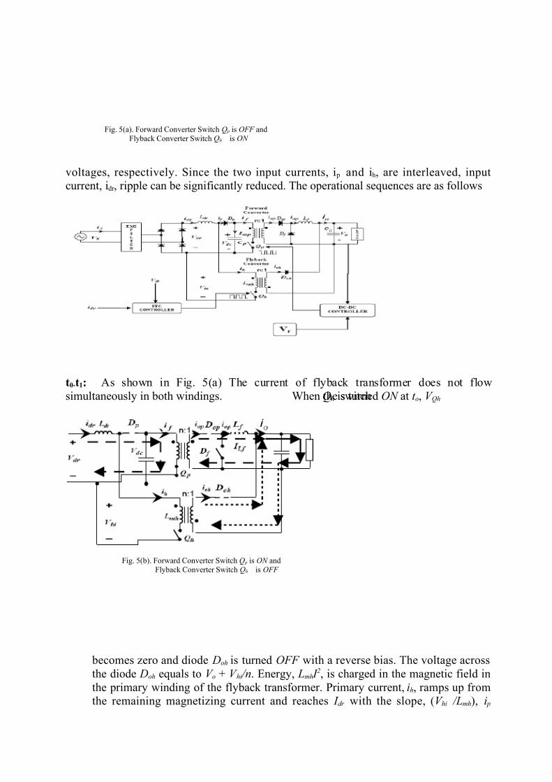
voltages, respectively. Since the two input currents, ip and ih, are interleaved, inputcurrent, idr , ripple can be significantly reduced. The operational sequences are as follows
t0-t1: As shown in Fig. 5(a) The current of flyback transformer does not flowsimultaneously in both windings. When the switchQh is turned ON at t o, V Qh
becomes zero and diode Doh is turned OFF with a reverse bias. The voltage acrossthe diode Doh equals to V o + V hi/n. Energy, LmhI
2, is charged in the magnetic field inthe primary winding of the flyback transformer. Primary current, ih, ramps up fromthe remaining magnetizing current and reaches I dr with the slope, (V hi /Lmh), ip
Fig. 5(a). Forward Converter Switch Qp is OFF andFlyback Converter Switch Qh is ON
Fig. 5(b). Forward Converter Switch Qp is ON andFlyback Converter Switch Qh is OFF
8/7/2019 Parallel Power Flow ACDC Converter With High Input Power Factor and Tight Voltage Regulation
decreases with a slow current tail, and slowly decreases until ip reaches zero. At thesame time the forward converter switch Qp is OFF because, as the switch Qh is ON
the potential at he junction of diode Dp and input inductor Ldr i.e. V Ldr >V hi, the diodeDp is reverse biased. The diode Dop is also reverse biassed due to the polarity of theforward transformer and a negative voltage of -nV o. The voltage across the output
inductor is V L= -V o and the inductor current iLf decreases and iLf along with ioh,circulates through diode Df , and supplied to load.t1-t2: The primary current of flyback converter increases by V dr /(Lmh + Ldr ). The voltage
across switch Qp decreases from 2V dr to V d r . The input inductor current ramps up totill switch Qh is OFF .
t2-t3: As shown if Fig. 5(b), when the switch Qh is turned OFF , Doh is turned ON withforward bias. The current in the primary winding ceases to flow. The stored energyis transferred to the secondary winding. At this time, the switch voltage, V Qh,becomes V hi+nV o, ip becomes idr and decreases depending on input voltage, and thesecondary current decreases with the slope (n2V o/Lmh). When the switch Qp is ON ,the diode Dp is forward biassed because the
Fig. 6. Operational waveforms of proposed parallel PFC TopologyFig. 8. Current Waveforms in switching period
8/7/2019 Parallel Power Flow ACDC Converter With High Input Power Factor and Tight Voltage Regulation
potential at junction between the diode and inductor is V Ldr <V hi+nV o. The primarycurrent of forward transformer ramps up and the energy stored in the primarywinding is instantaneously transferred to secondary, because of the same polarity of
the forward transformer. The diode Dop is forward biassed and diode Df is reversedbiassed. The output inductor current iLf increases along with ioh which is delivered toload.
The current slope through the magnetizing inductor when the switch Qh is turned off isgiven as
off
mh
omh T
L
nV i −=∆ (7)
Where, Toff is the turn-off time. Similarly, the change of the flyback converter inputcurrent ip through a diode is
off dr
dr
p T L
V Vdc
i
−
−=∆ (8)Based on two slopes of imh and ip, the tailed diode current mode in which the diodecurrent has current tail is defined as shown Fig. 7 when the slope of imh is greater than thatof ip
mh
dr odcmhdr
L
LnV V Lv
−> (9)
In continuous conduction input inductor current mode, when the MOSFET is switchedon, the diode Dp is forced into reverse recovery at a high rate of change in the diodecurrent ip. In this tailed mode operation, however, the diode current slowly decreases so
that the reverse recovery effect can be minimized.To analyze the flyback converter operation, an open loop duty ratio is obtained from(2) as
odr
ohopen
nV v
nV D
+=,
(10)Where, input voltage t SinV v sdr ω2= . Assuming two input currents of each converter have the waveforms shown in Fig. 8, two currents depend on the duty ratio from (10)
8/7/2019 Parallel Power Flow ACDC Converter With High Input Power Factor and Tight Voltage Regulation
Fig. 9 shows those current waveforms and harmonic components. Now, instantaneouspowers through the diode Dp and the transformer T2 are calculated by using the inputinductance and the magnetizing inductance
].[2,
upLL
LLP
dr mh
dr mh
pup +
+= (15)
].[2,
upLL
LP
dr mh
mh
puh += (16)
Where, Lmh and Ldr denote the magnetizing inductance of T2 and input inductance,respectively, and the input total power ].[1,,, upP P P puhpuppuin =+= . On the other
hand, by employing the open loop duty ratio Dopen, h, two instantaneous powers can bederived by hsspdcp it SinI V iV P −== ω 22. (17)
pinh P P P −= (18)Where, }2cos1{ t I V P ssin ω −= . The relations between two inductances and two inputaverage powers of two converters are expressed as
aveh
avep
mh
dr mh
P
P
L
LL
,
,=
+(19)
,1,
,
−=aveh
avep
mhdr P
P LL (20)
The output currents of the two cells are given by turns ratio f op ini .= (21) hoh ini .=
Since the output load current io may contain only dc and switching frequencomponents, the harmonic contents for the primary current of the flyback converter-I isexpressed as
,o
ssohopo
V
I V iii =+= (22)
xhxf ii ,, = (23)
Where, x(= 2 , 4, 6, etc.) is harmonic order. From (23), the dc-link capacitor current canbe estimated as a second harmonic
.2)( 2,2,2, t Cosiii hpdc ω +−= (24)Therefore, the voltage ripple of the dc-link capacitor is obtained as
t SinC
iiV
p
hp
rippledc ω
ω
22
2,2,
,
+−= (25)
Where, Cp is the capacitance of the dc-link capacitor.
8/7/2019 Parallel Power Flow ACDC Converter With High Input Power Factor and Tight Voltage Regulation
To control the proposed approach, two control stages are required for PFC and outputvoltage regulation as shown in Fig. 10. Flyback converter is regulated by a conventional
PFC controller which consists of inner input current loop and outer dc-link voltage [16]to obtain high power factor Fig. 10(a). DC-link voltage is 1.414*Vs, which is better toreduce the voltage across drain-source of MOSFET Qp [16]. Based on the PFC controller,a feed-forward control block is added to improve input current shape. Since the open loopduty ratio Dopen,h of the PFC cell is calculated from (10), the final duty ratio for the switchgate input is obtained as
Dh= Dopen,h + Dpi (26)
where Dpi, is the closed loop duty ratio obtained from S-R flip flop current controller. Theoutput Dpi of the S-R flip flop current regulator containing a small amount of variationsprovides the correction to the final duty ratio. On the other hand, output voltage Vo
control is achieved by forward converter. Fig. 10(b) shows a simple PI voltage controller with a open loop duty ratio Dopen,h which is calculated similarly to
Dopen,p in terms of power ratings of each converter pupodr
pupo
popenP nV v
P nV D
.
.
,+
=
(27)Final duty ratio Dp is obtained by adding the duty ratio Dpi from controller with Dopen,p.
The output voltage control response is much faster than single stage scheme since twoconverters are employed for separate control function.
V.Design Example
The proposed PFC circuit is designed according to the following parameters.Total output power (Po) = 200 [W]Input voltage (Vs) = 150 [V]Output voltage (Vo) = 48 [V]
Fig. 10. Converter Controls
8/7/2019 Parallel Power Flow ACDC Converter With High Input Power Factor and Tight Voltage Regulation
Power rating =90.6 [W]Magnetizing inductance (Lmh) = 1.2 [mH]
The proposed scheme provides small input inductor since the inductor current dependson, dc-link voltage is smaller so that the voltage stress on the switch of the forwardconverter is less, the power rating of DC/DC stage is a bit higher than average power dueto lower harmonic components, and the diode reverse recovery loss is minimized because
of the tailed diode conduction mode.
The simulation results of the proposed topology are shown in Fig. 10. Unity power factor and tight output voltage (48 V) regulation can be achieved. The dc-link voltage is1.414*Vs=325V, and the voltage ripple of the dc-link is 3.4 V which mainly depends onthe dc-link capacitance. Fig. 11 shows the analysis of the circuit currents. The primaryside current of forward converter has 2nd and 4th harmonics due to the harmonics on theflyback converter. Two control systems are implemented to prove the proposed scheme.In the diode current, current tail is appeared when the diode is turned off. 5.2% inputcurrent THD and 86% efficiency are obtained.
8/7/2019 Parallel Power Flow ACDC Converter With High Input Power Factor and Tight Voltage Regulation
A parallel-connected single phase power factor correction (PFC) topology usingforward converter and a flyback converter has been proposed. It has been shown thatoutput voltage regulation is, achieved by DC/DC cell and the input power factor correction is achieved by AC/DC PFC cell. These
8/7/2019 Parallel Power Flow ACDC Converter With High Input Power Factor and Tight Voltage Regulation
two power stages have 60% and 40% power sharing, respectively. The proposedapproach offers the following advantages: smaller size passive components, lower voltage-ampere rating of DC/DC stage, and higher efficiency. Simulation demonstrate the capability of the proposed scheme.
R EFERENCES
[1] W. F. Ray and R. M. Davis, “The definition and importance of power factor for
power electronic converters,” Proc. European conference on Power Electronics andApplications (EPE), 1989, pp. 799-805.
[2] L. Huber, J. Zhang, M. M. Jovanovic, and F. C. Lee, “Generalized topologies of “Single-stage input-current-shaping circuits,” IEEE Trans. Power Electron., vol. 16,pp. 508–513, July 2001.
[3] R. Redl, L. Balogh, and N. O. Sokal, “A new family of single-stage isolated power-factor correctors with fast regulation of the output voltage ,” in Proc. PESC’94, 1994,pp. 1137–1144.
[4] R. Erickson, M. Madigan and S. Singer, “Design of a simple high power factor rectifier based on the flyback converter ,” IEEE Applied Power ElectronicsConference, 1990, pp. 792-801.
Fig. 10. Simulation results of the proposed approach
8/7/2019 Parallel Power Flow ACDC Converter With High Input Power Factor and Tight Voltage Regulation
[5] G. Choe and M. Park, “Analysis and control of active power filter with optimized injection,” IEEE Power Electronics Specialists Conference, 1986, pp. 401-409.
[6] K. K. Sen, A. E. Emanuel, “Unity power factor single phase power conditioning ,”IEEE Power Electronics Specialists Conference, 1987, pp. 516-524.
[7] W. Tang, Y. Jiang, G. C. Hua, F. C. Lee, and I. Cohen, “Power factor correction with
flyback converter employing charge control ,” in Proc. APEC’93, 1993, pp. 293–298.[8] R. Srinivasan and R. Oruganti, “Single phase parallel power processing scheme with
power factor control ,” Power Electron. Drive Syst., pp. 40–47, 1995.[9] Y. Jiang and F. C. Lee, “Single-stage single-phase parallel power factor correction
scheme,” in Proc. PESC’94, 1994, pp. 1145–1151.[10] W. A. Tabisz, M. M. Jovanovi}, and F. C. Lee, “Present and future of distributed
power systems,” Proc. IEEE Appl. Power Electron. Conf., 1992, pp. 11-18.[11] G. Suranyi, “The value of distributed power ,” Proc. IEEE Appl. Power Electron.
Conf., 1996, pp. 104-110.[12] B.A. Miwa, D.M. Otten, and M.F. Schlecht, "High efficiency power factor
correction using interleaving techniques," Proc. IEEE Appl. Power Electron. Conf.,
1992, pp. 557- 568.[13] J. Zhang, M. M. Jovanovic, and F. C. Lee, “Comparison between CCM single-stageand two-stage boost converter ,” in Proc. APEC’99, 1999, pp. 335–341.
[14] M. Daniele, P. K. Jain, and G. Joos, “A single-stage power-factor-corrected AC/DC
converter ,” IEEE Trans. Power Electron., vol. 14, pp. 1046–1055, Nov. 1999.