Materials Science Fall, 2008 Page 431 PART III: ELECTROMAGNETIC PROPERTIES 436 CHAPTER 13: METALS 438 13.1 The Electrical Conductivity 438 13.1.1 Ohm's Law 438 13.1.2 The local form of Ohm's Law: resistivity and conductivity 439 13.1.3 The influence of symmetry on the conductivity 440 13.2 The Mechanism of Conduction by Electrons 441 13.3 Conductor Type and Quality 443 13.3.1 Band structure and conductor type 443 13.3.2 The three classes of metals 445 13.3.3 The difference in conductivity between classes of metals 446 13.4 The Influence of Temperature and Purity 448 13.4.1 The electron mean free path 448 13.4.2 Matthiesen's Rule 449 13.4.3 The thermal resistivity of the crystal lattice 449 13.4.4 The contribution of solutes and imputities 450 13.4.5 The total resistivity 451 13.4.6 The resistivity of alloys and two-phase mixtures 452 CHAPTER 14: SEMICONDUCTORS 454 14.1 Introduction 454 14.2 Intrinsic Semiconductors 455 14.2.1 The band structure of an intrinsic semiconductor 455 14.2.2 The free electron density in an intrinsic semiconductor 456 14.2.3 Electron holes in intrinsic semiconductors 458 14.2.4 The intrinsic carrier density and the Fermi energy 459 14.2.5 The conductivity of an intrinsic semiconductor 460 14.3 Extrinsic Semiconductors 461 14.3.1 Types of extrinsic semiconductors 461 14.3.2 Donors: n-type semiconductors 461 14.3.3 Acceptors: p-type semiconductors 462 14.3.4 Carrier density in an n-type semiconductor 464 14.3.5 Conductivity in an n-type semiconductor 467 14.3.6 Conductivity in a p-type semiconductor 468 14.3.7 Compensation between active sites 469 14.3.8 Degenerate semiconductors 470 14.3.9 Carrier lifetime 470
Transcript
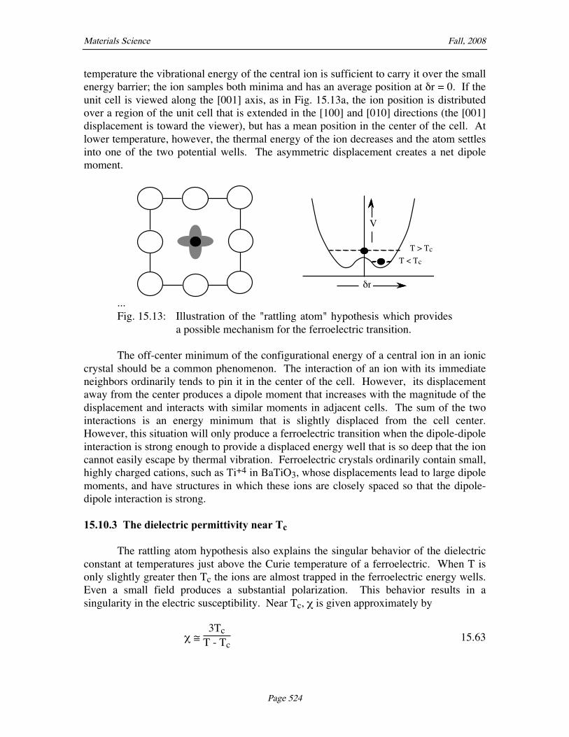
Materials Science Fall, 2008
Page 431
PART III: ELECTROMAGNETIC PROPERTIES 436
CHAPTER 13: METALS 438
13.1 The Electrical Conductivity 438 13.1.1 Ohm's Law 438 13.1.2 The local form of Ohm's Law: resistivity and conductivity 439 13.1.3 The influence of symmetry on the conductivity 440
13.2 The Mechanism of Conduction by Electrons 441
13.3 Conductor Type and Quality 443 13.3.1 Band structure and conductor type 443 13.3.2 The three classes of metals 445 13.3.3 The difference in conductivity between classes of metals 446
13.4 The Influence of Temperature and Purity 448 13.4.1 The electron mean free path 448 13.4.2 Matthiesen's Rule 449 13.4.3 The thermal resistivity of the crystal lattice 449 13.4.4 The contribution of solutes and imputities 450 13.4.5 The total resistivity 451 13.4.6 The resistivity of alloys and two-phase mixtures 452
CHAPTER 14: SEMICONDUCTORS 454
14.1 Introduction 454
14.2 Intrinsic Semiconductors 455 14.2.1 The band structure of an intrinsic semiconductor 455 14.2.2 The free electron density in an intrinsic semiconductor 456 14.2.3 Electron holes in intrinsic semiconductors 458 14.2.4 The intrinsic carrier density and the Fermi energy 459 14.2.5 The conductivity of an intrinsic semiconductor 460
14.3 Extrinsic Semiconductors 461 14.3.1 Types of extrinsic semiconductors 461 14.3.2 Donors: n-type semiconductors 461 14.3.3 Acceptors: p-type semiconductors 462 14.3.4 Carrier density in an n-type semiconductor 464 14.3.5 Conductivity in an n-type semiconductor 467 14.3.6 Conductivity in a p-type semiconductor 468 14.3.7 Compensation between active sites 469 14.3.8 Degenerate semiconductors 470 14.3.9 Carrier lifetime 470
Materials Science Fall, 2008
Page 432
14.4 The n-p Junction 471 14.4.1 The Fermi energy at a heterogeneous junction 471 14.4.2 Response to an Impressed Potential 475
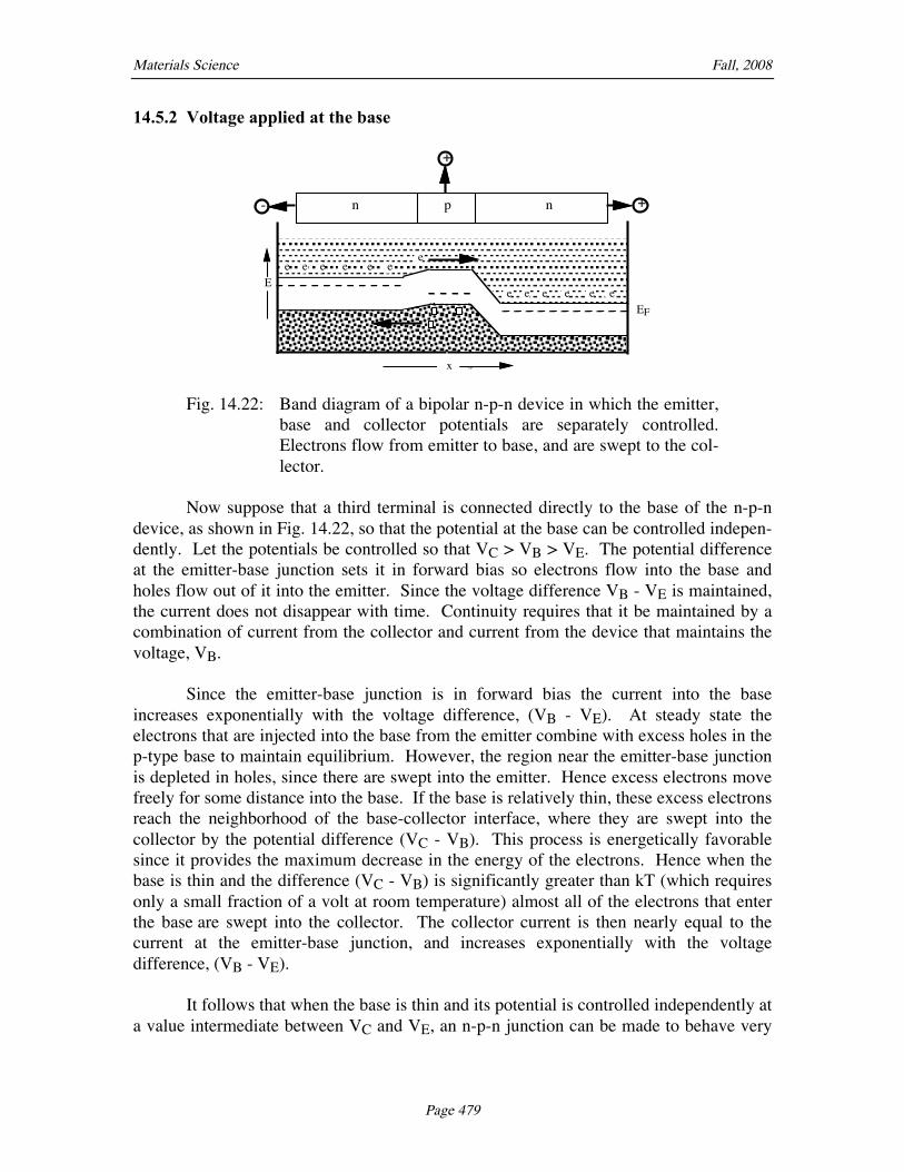
14.5 The n-p-n Junction 477 14.5.1 Voltage applied at the collector 477 14.5.2 Voltage applied at the base 479 14.5.3 Two applications of the bipolar transistor 480
15.1 Introduction 497 15.1.1 Types of insulators 497 15.1.2 Properties and applications of insulators 498
15.2 The Dielectric Constant 499 15.2.1 The capacitance 499 15.2.2 The dielectric permittivity 499 15.2.3 The electric displacement 500 15.2.4 The dielectric constant 500 15.2.5 The dielectric constant of a crystalline solid 501
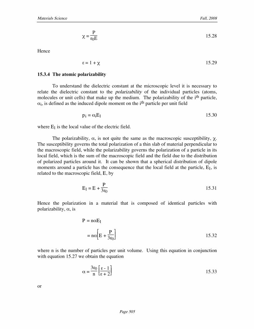
15.3 Polarizability 502 15.3.1 The dipole field in an insulator 502 15.3.2 The dielectric constant of a polarized medium 504 15.3.3 The dielectric susceptibility 504 15.3.4 The atomic polarizability 505
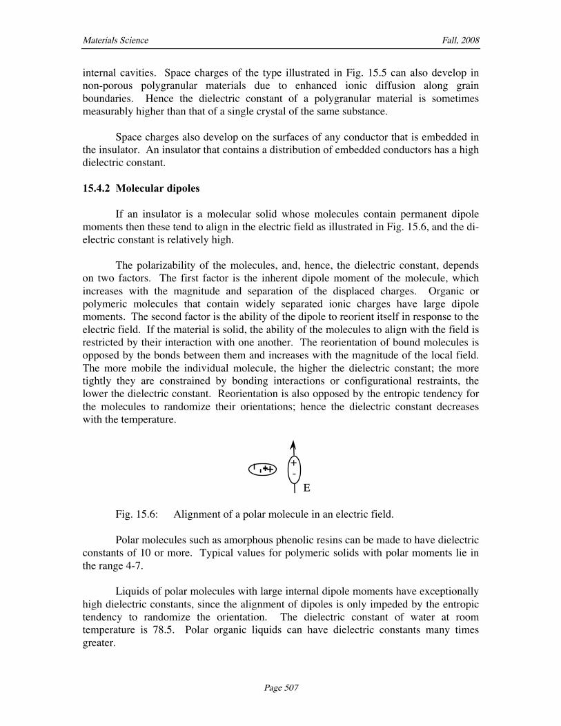
15.4 Origin of the Dielectric Constant 506 15.4.1 Space charges 506 15.4.2 Molecular dipoles 507 15.4.3 Ionic displacements 508
Materials Science Fall, 2008
Page 433
15.4.4 Atomic polarization 508
15.5 Frequency Dependence of the Dielectric Constant 509 15.5.1 The relaxation time for polarization 509 15.5.2 Relaxation times of the common polarization mechanisms 511
15.6 Dielectric Loss 512 15.6.1 The phase shift of an oscillating field 512 15.6.2 The dielectric loss tangent 513 15.6.3 The dielectric current 513 15.6.4 The dielectric power loss 514 15.6.5 The influence of microstructure and frequency 515
15.7 The Dielectric Strength 516 15.7.1 The dielectric strength and the critical voltage 516 15.7.2 Cascade breakdown 516 15.7.3 Thermal breakdown 517
15.9 Dielectrics with Permanent Dipole Moments 521
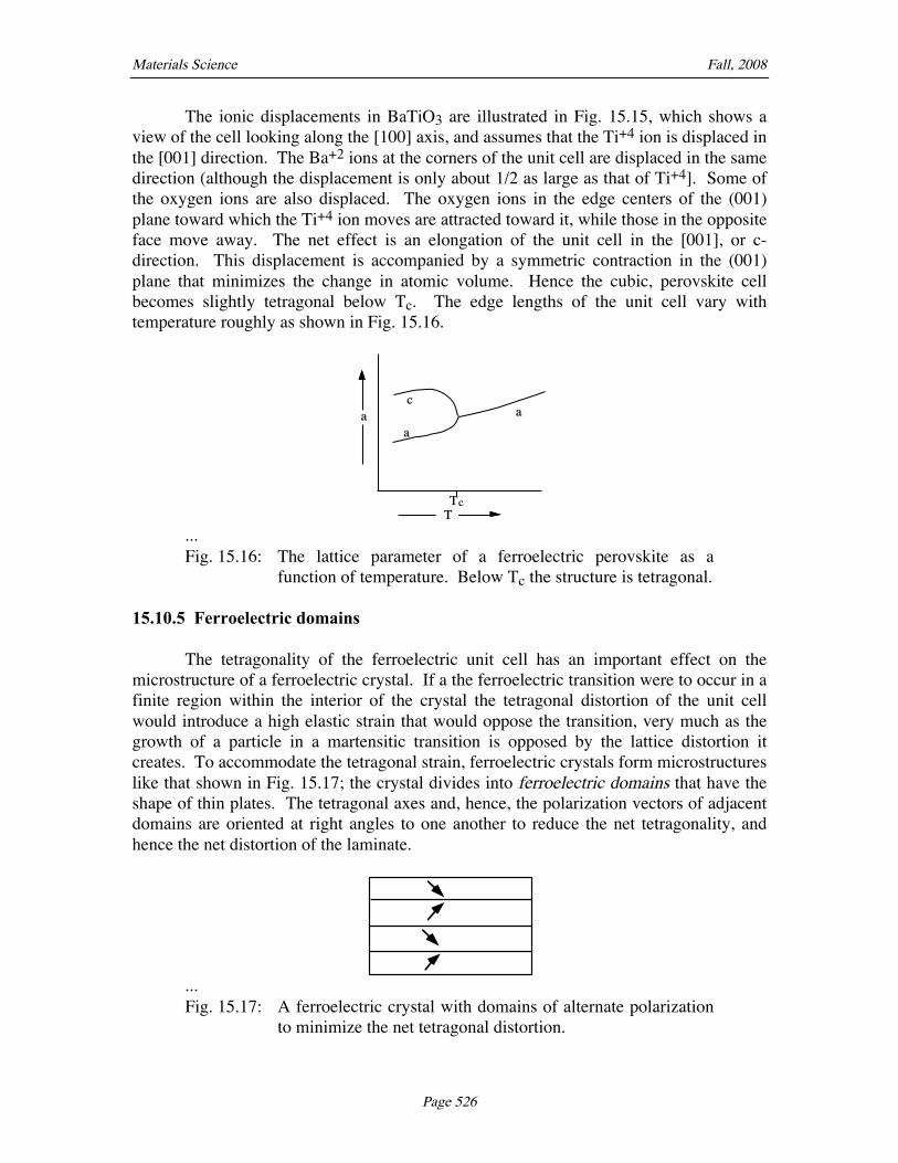
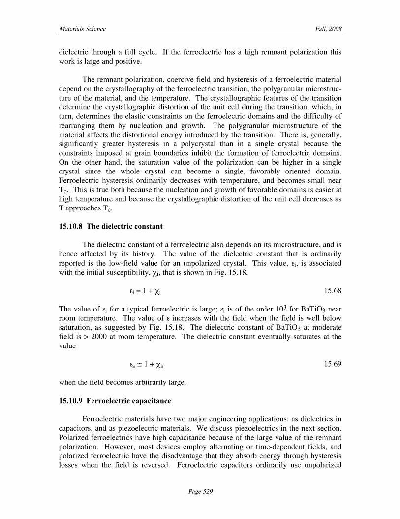
15.10 Ferroelectric Materials 522 15.10.1 Characteristics of the ferroelectric transition 522 15.10.2 Source of the ferroelectric transition 523 15.10.3 The dielectric permittivity near Tc 524 15.10.4 Crystallographic distortion below the Curie temperature 525 15.10.5 Ferroelectric domains 526 15.10.6 The response of a ferroelectric to an applied electric field 527 15.10.7 The electric displacement and the hysteresis curve 528 15.10.8 The dielectric constant 529 15.10.9 Ferroelectric capacitance 529
15.11 Piezoelectric Materials 530 15.11.1 The piezoelectric effect in a polar insulator 530 15.11.2 The piezoelectric effect in a non-polar insulator 531 15.11.3 Crystallographic criterion for piezoelectricity 531 15.11.4 Applications of piezoelectrics 532
CHAPTER 16: PHOTONIC MATERIALS 533
16.1 Introduction 533
16.2 Electromagnetic Waves in Free Space 537 16.2.1 Dipole Waves 537
Materials Science Fall, 2008
Page 434
16.2.2 The Electromagnetic Spectrum 540 16.2.3 Plane Waves and Polarization 542 16.2.4 Electromagnetic Waves as Solutions to Maxwell's Equations 543 16.2.5 Photons 544 16.2.6 Interference 545
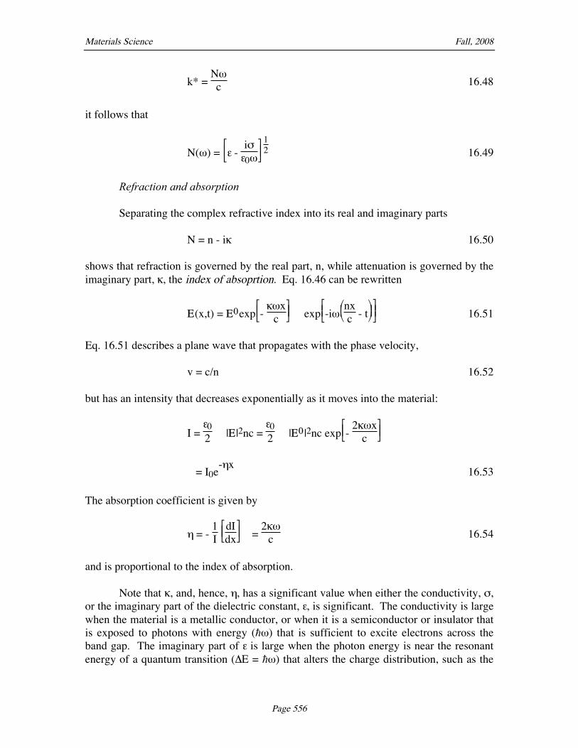
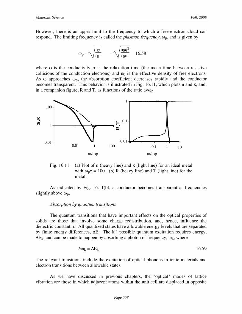
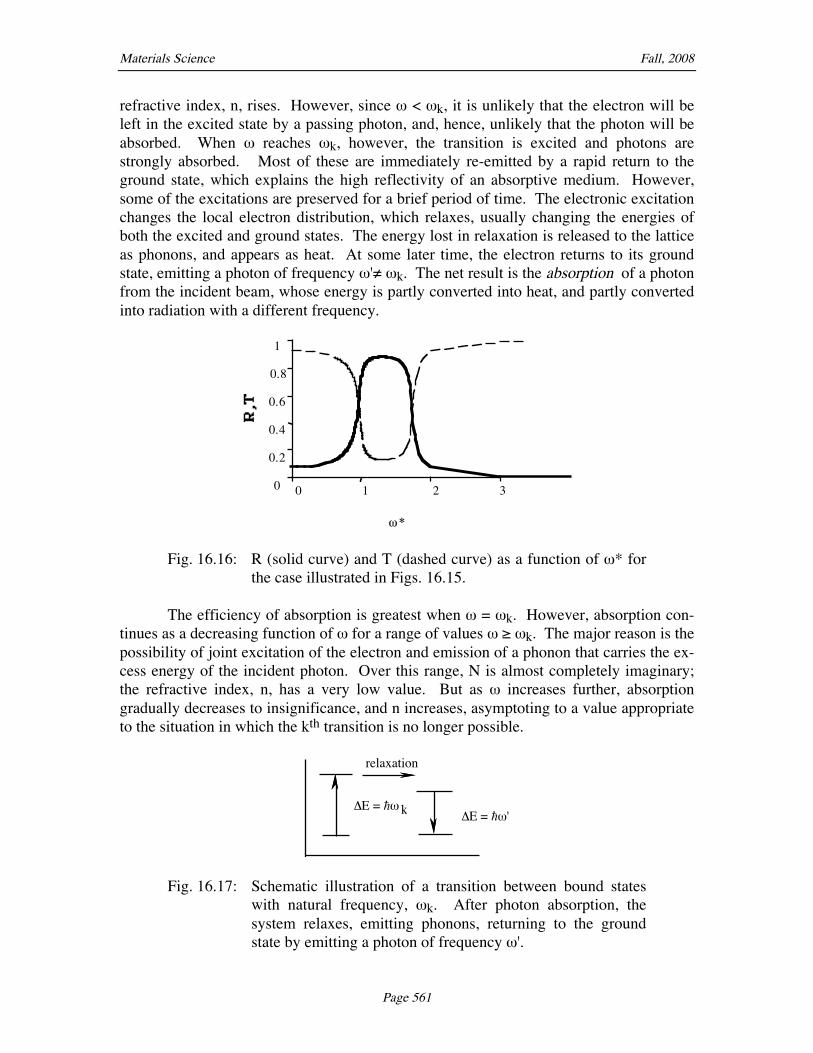
16.3 The Propagation of Light through Solids 548 16.3.1 Wave Propagation in Solids 548 16.3.2 Refraction 549 16.3.3 Absorption; The Complex Refractive Index 554 16.3.4 The Mechanisms of Complex Refraction 557 16.3.5 Scattering of electromagnetic waves 564 16.3.6 Reflection and Refraction at an Interface 568
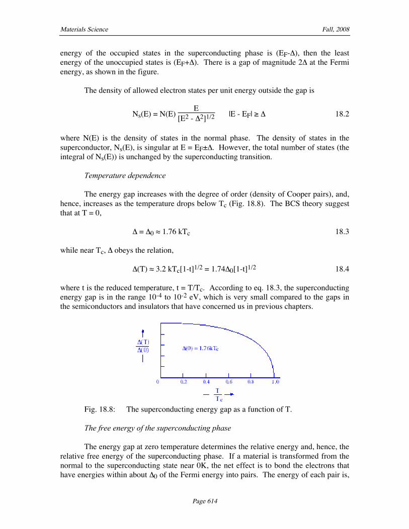
18.2 The Superconducting Phase 610 18.2.1 Cooper pairs 611 18.2.2 The energy gap 613 18.2.3 The coherence length 615
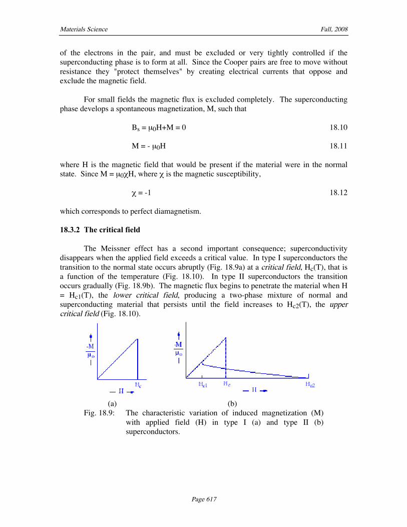
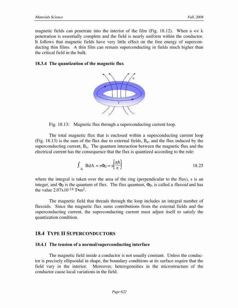
18.3 The Meissner effect and the critical field 616 18.3.1 The Meissner Effect 616 18.3.2 The critical field 617 18.3.3 The penetration depth 620 18.3.4 The quantization of the magnetic flux 622
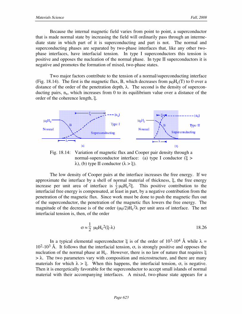
18.4 Type II Superconductors 622 18.4.1 The tension of a normal/superconducting interface 622 18.4.2 The magnetic behavior of a type II superconductor 624 18.4.3 Sources of type II behavior 627
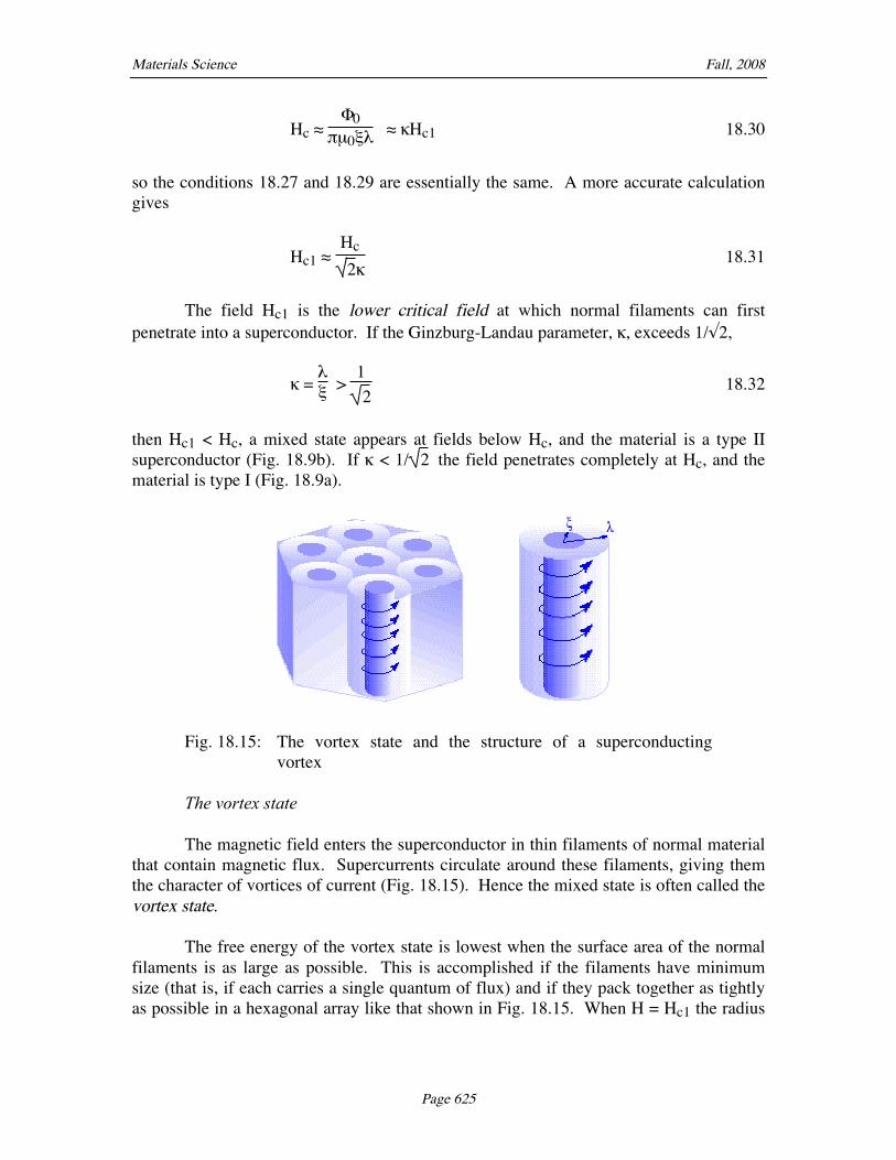
18.5 The Critical Current 629 18.5.1 The critical current of a type I conductor 630 18.5.2 Persistent currents in type I conductors 631 18.5.3 The critical current of a type II superconductor 631 18.5.4 Flux creep and vortex melting 634
18.6 Superconductor Junctions 636 18.6.1 Single electron (Giaever) tunneling 637 18.6.2 Paired electron (Josephson) tunneling 637 18.6.3 Superconducting quantum interference 639
P a rP a r t I I I : E l e c t r o m a g n e t i c P r o p e r t i e st I I I : E l e c t r o m a g n e t i c P r o p e r t i e s "When I studied physics in Taiwan," said Huang, "we called it Wu Li ... It means 'patterns of organic energy'." - Gary Zukov, "The Dancing Wu Li Masters" The electromagnetic properties of a material are those that govern its response to electric fields, magnetic fields, and electromagnetic radiation. The most basic electromagnetic property is the ability to conduct electricity in response to an electric field. It is useful to divide solids into three classes on the basis of their electrical conductivity: metals, semiconductors and insulators. Metals conduct electricity. While all metals do this, their conductivity varies with their kind, purity and temperature. We shall first consider why some pure metals are better conductors than others, and then discuss how the conductivity is decreased when the metal is alloyed or its temperature is raised. Semiconductors, as the name implies, are relatively poor conductors that are not particularly useful for transporting current. Despite this fact semiconductors have widespread and critical applications in electronic devices. They are so useful because their electrical properties can be tightly controlled. Both the type of the carrier that moves electrical current through a semiconductor and the magnitude of its conductivity can be changed by adjusting the composition or microstructure. Semiconductors can be made so that neighboring volumes have different conducting characteristics. The junctions between dissimilar regions have characteristic electrical properties that are exploited in microelectronic devices. Insulators are very poor conductors. They are used to isolate conductors from one another. However, they never do this perfectly. Not only is there a maximum voltage that an insulator can withstand before breakdown, but small shifts of charge in the interior of the insulator cause it to behave as a dielectric, supporting electric fields that influence the behavior of any conductors that are in its immediate neighborhood. The dielectric constant of an insulator governs many of its engineering applications. Materials with very high dielectric constants are useful in capacitors that store energy, while materials with low dielectric constants are preferred for electronic circuits. It is natural to move from the discussion of insulators to a discussion of the optical properties of materials, since the materials that are most commonly used for their optical properties are electrical insulators that are transparent to light. The optical properties of a material govern its ability to transmit light, emit light, and convert light into other forms, such as heat or electrical current. With very few exceptions the
Materials Science Fall, 2008
Page 437
materials that transmit light are electrical insulators. Their critical property is the index of refraction, which is related to the dielectric constant and governs the velocity of light within the material. The most common application of transparent materials is in window glass. The most exciting current application is in optical fibers, which confine and transmit light. The materials that emit light do so because of electronic transitions in the body of the material. Such materials are used in light-emitting doides (LED), which are, essentially, efficient light bulbs, and in the solid state lasers that produce beams of coherent light to transmit information or energy in optical form. The materials that convert light absorb it to create either heat or electrical current. Among the most interesting are the photoconductors, which are semiconductors whose conductivity increases dramatically when they are illuminated with light. Photoconductors are critical elements in photoelectric devices and photocopying machines. The third set of properties we shall consider are magnetic properties. While all materials respond to magnetic fields, the response is small unless the material is made up of atoms that have net magnetic moments, and unless these magnetic moments align to cause ferromagnetism. Ferromagnetic materials are used in a wide variety of important devices that range from electric transformers to acoustic speakers to magnetic films and tapes that store information. Finally, we consider superconducting materials, which are metals that have essen-tially zero resistance to electrical current. While the most important property of a superconductor is its electrical conductivity, it is best to defer the discussion of superconductivity until after we treat magnetic properties. Superconductors have a unique magnetic behavior, the exclusion of magnetic fields, that is intimately associated with their superconductivity. Superconductors are relatively new to engineering, but are used more and more widely in high field magnets, energy storage devices, and, in the form of superconductor-insulator junctions, in microelectronic devices that have a number of interesting applications.
Materials Science Fall, 2008
Page 438
C h a p t e r 1 3 : M e t a l sC h a p t e r 1 3 : M e t a l s
I am a copper wire slung in the air, Slim against the sun I make not even a clear line of shadow. Night and day I keep singing - humming and thrumming; It is love and war and money; it is the fighting and the tears, the work and want, Death and laughter of men and women passing through me, carrier of your speech, In the rain and the wet dripping, in the dawn and the shine drying, A copper wire. - Carl Sandburg, "Under a Telephone Pole"
13.1 THE ELECTRICAL CONDUCTIVITY 13.1.1 Ohm's Law
+ -
V Ex
Ie-
x
L
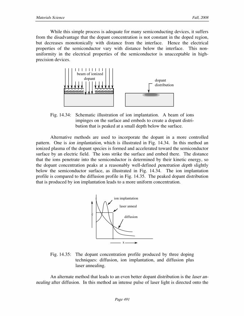
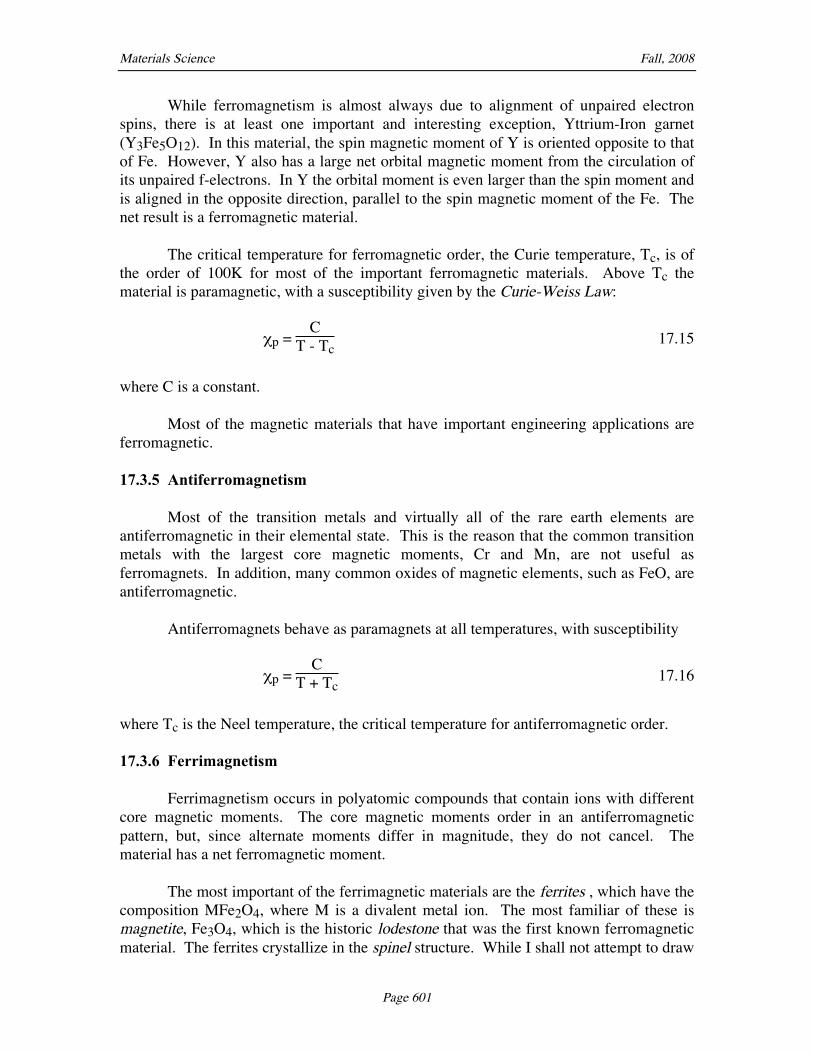
Fig. 13.1: Illustration of current flow in a bar whose ends are connected to the positive and negative terminals of a battery. The cur-rent, I, flows down the gradient in the potential, V. The elec-tron flow is in the opposite direction.
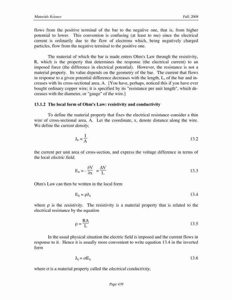
The conduction of electricity is described by a familiar relation that is known as Ohm's Law. Let the two ends of a solid bar be held at different electrical potentials, for example, by connecting them to the terminals of a battery. A possible configuration is shown in Fig. 13.1. An electrical current flows through the bar. Its magnitude is given by the relation ÎV = IR 13.1 where ÎV is the voltage difference between the two ends of the bar, I is the electrical cur-rent, and R is the electrical resistance. By historical convention, the electrical current
Materials Science Fall, 2008
Page 439
flows from the positive terminal of the bar to the negative one, that is, from higher potential to lower. This convention is confusing (at least to me) since the electrical current is ordinarily due to the flow of electrons which, being negatively charged particles, flow from the negative terminal to the positive one. The material of which the bar is made enters Ohm's Law through the resistivity, R, which is the property that determines the response (the electrical current) to an imposed force (the difference in electrical potential). However, the resistance is not a material property. Its value depends on the geometry of the bar. The current that flows in response to a given potential difference decreases with the length, L, of the bar and in-creases with its cross-sectional area, A. [You have, perhaps, noticed this if you have ever bought ordinary copper wire; it is specified by its "resistance per unit length", which de-creases with the diameter, or "gauge" of the wire.] 13.1.2 The local form of Ohm's Law: resistivity and conductivity To define the material property that fixes the electrical resistance consider a thin wire of cross-sectional area, A. Let the coordinate, x, denote distance along the wire. We define the current density,
Jx = IA 13.2
the current per unit area of cross-section, and express the voltage difference in terms of the local electric field,
Ex = - ∆V∆x =
ÎVL 13.3
Ohm's Law can then be written in the local form Ex = ®Jx 13.4 where ® is the resistivity. The resistivity is a material property that is related to the electrical resistance by the equation
® = RAL 13.5
In the usual physical situation the electric field is imposed and the current flows in response to it. Hence it is usually more convenient to write equation 13.4 in the inverted form Jx = ßEx 13.6 where ß is a material property called the electrical conductivity,
Materials Science Fall, 2008
Page 440
ß = 1® 13.7
Using equations 13.3 and 13.6, Ohm's Law can be re-written
Jx = - ß∆V∆x 13.8
which has exactly the same form as Fick's Law for diffusion or Fourier's Law for heat conduction. The electrical conductivity is the diffusivity that governs the net electrical flux that is induced by the potential gradient, ∆V/∆x. The potential gradient measures the local deviation from electrical equilibrium. When the potential is constant, there is no net current flow. 13.1.3 The influence of symmetry on the conductivity Just as in the case of the diffusivity and thermal conductivity, it is only correct to speak of the conductivity of a material when the material has cubic or isotropic symmetry. Both the current flux, J , and the electric field, E, are vectors, and they need not necessarily be parallel. In the most general case the current flux in the x-direction depends on all three components of the electric field through a relation of the form Jx = ßxxEx + ßxyEy + ßxzEz 13.9 Similar relations govern the currents in the y and z directions, Jy and Jz. Hence a material has nine electrical conductivities, ßij, where i and j take each of the three values x, y, z. Whatever the symmetry of the material, the conductivities obey the symmetry relations ßij = ßji 13.10 that is, ßxy = ßyx, etc., so that there are, in the most general case, six independent conductivities, all of which must be evaluated to determine the current that flows in response to an electric field. However, as we discussed in Chapter 9 in connection with the diffusivity and the thermal conductivity, the number of independent values of the conductivity is reduced further by the symmetry of the material. If the material is cubic or isotropic, ßxy = ßxz = ßyz = 0 ßxx = ßyy = ßzz = ß 13.11 In this case, J = ßE 13.12
Materials Science Fall, 2008
Page 441
In a cubic material the current flow is in the direction of the electric field, and the conductivity is given by the single-valued material property, ß. The material is cubic or isotropic when its crystal structure is cubic or isotropic (amorphous). A material is also isotropic in the macroscopic sense when it is polygranular and contains a great many grains that are randomly oriented. Since most of the materials of engineering interest fall into one of these two categories, we can ordinarily assume a single, well-defined value of the conductivity, and shall do so in the following. However, there are important exceptions. For example, a hexagonal crystal has two independent conductivities. One governs current flow in the basal plane of the hexagonal cell and the other governs flow perpendicular to the basal plane. The values of these two conductivities can differ dramatically. Graphite is a particularly striking case, since it conducts electricity readily in the basal plane of its hexagonal unit cell, but is a poor conductor in the perpendicular direction. The anisotropy of the crystal may be reflected in the macroscopic properties of a polygranular or composite material in which it appears. A typical graphite fiber composite material contains graphite fibers in a matrix that is an insulating polymer. Since the fibers are rolled sheets of graphite with the fiber axis in the basal plane, a graphite-fiber reinforced composite is highly conductive in the direction parallel to the fibers, but insulating in the perpendicular direction. This strong anisotropy affects its usefulness in electronic devices and engineering systems that are subject to electric fields. 13.2 THE MECHANISM OF CONDUCTION BY ELECTRONS While there are ionic materials that conduct electricity by the diffusion of ions, and many semiconductors whose conductivity is best attributed to positive "holes" (empty electron states), in the vast majority of cases the conduction of electricity is due to the flow of electrons. We briefly discussed the flow of electrons in Section 10.4.2, which treated the conduction of heat by mobile electrons. As we pointed out there, conduction electrons travel through the solid at high speed in all directions. The electrons are not affected by the equilibrium crystal lattice, since they are in electron states that are compatible with the crystalline arrangement of the ion cores. However, they do interact with deviations from the equilibrium arrangement of ion cores, as provided, for example, by displacements of the ion cores due to lattice vibrations and by solute or impurity atoms that disturb the local charge distribution and distort the lattice. Consider the situation shown in Fig. 13.2, where an electron travels along the x-direction under the influence of an electric field, E, that points in the negative x-direction. The electric field exerts a force on the electron that is equal to F = qE = - eE 13.13
Materials Science Fall, 2008
Page 442
where q = - e is the charge on the electron. In the example shown in the figure this force accelerates the electron in the positive x-direction. Let vx be the velocity of the electron in the absence of the field. The field accelerates the electron, so that its velocity increases with time according to the relation
vx(t) = vx + ∂v(t) = vx + Ftm
= vx - eEtm 13.14
As the electron moves through the material, it periodically collides with displaced atoms or solutes. Under the usual assumption that the electron equilibrates after each collision (Section 10.4) its velocity along the bar returns to vx. It follows that the velocity of the varies with time in the jerky manner shown in the plot in Fig. 13.2.
x
x
xx
x
xEx
v
x
´∂v¨
vx
... Fig. 13.2: An illustration of the motion of an electron under the action
of an electric field. The upper figure shows the variation of the velocity with time.
In the absence of a field, electrons in states near the Fermi level travel at a Fermi velocity (vF) that is a significant fraction of the speed of light. However, they are equally likely to move in the positive and negative directions, so the average x-velocity, ´vx¨, is zero. It follows that an applied field, E, produces the average velocity ´vx¨ = ´∂v¨ 13.15 where ´∂v¨ is called the drift velocity. Since the electron experiences a constant accelera-tion, - eE/m, between collisions, the drift velocity is
´∂v¨ = - eE†m
Materials Science Fall, 2008
Page 443
= - µE 13.16 where 2† is the average time-of-flight between collisions, and
µ = e†m 13.17
is called the mobility. The drift velocity is small compared to the speed of a free electron. The net current (J) across a plane perpendicular to the x-direction is the negative of the electron flux, the net number of electrons that cross per unit area per unit time.
J = - ne´∂v¨ = ne2E†
m
= neµE 13.18 where n is the density of mobile electrons. Comparing with Ohm's Law, equation 13.12, the conductivity is
ß = neµ = ne2†
m 13.19
Note that two factors determine the magnitude of the conductivity: the density of mobile electrons, n, and the electron mobility, µ. The carrier density, n, is a characteristic of the material, and determines whether a particular material is, inherently, a good conductor or a poor one. If n is small then, barring a superconducting transition, the material can never be a good conductor. It is the value of n that separates metals from semiconductors from insulators. On the other hand, a material with a high density of mobile carriers is not necessarily a good conductor. If the material is glassy, impure or highly alloyed then the electron mobility is small and the conductivity is relatively low. 13.3 CONDUCTOR TYPE AND QUALITY 13.3.1 Band structure and conductor type The mobile electrons that are primarily responsible for electrical conduction have two characteristics. First, they occupy states in the valence or excited bands of the solid that spread throughout the solid, so that they can move relatively freely. Even when the core states of a solid are only partly filled, as in the transition metals, the electrons that fill these states are localized near the ion cores and are relatively immobile. Second, the mobile electrons occupy states that are neighbored by empty states. An electron cannot be accelerated to a higher velocity, and, hence, higher kinetic energy, unless there are
Materials Science Fall, 2008
Page 444
empty electron states at that energy. In order for the electron to be accelerated continuously, there must be a spectrum of empty states nearby. As we saw in Chapter 2, the density of such states is determined by the band structure of the material. Metals are distinguished from semiconductors and insulators on the basis of whether the valence band is filled in the ground state. The two prototype cases are illustrated in Fig. 13.3. The figure on the left, 13.3a, illustrates the band structure of a semiconductor or insulator. In the ground state, that is, the state assumed at T = 0, the highest occupied band, the valence band, is just filled, while the lowest excited band, the conduction band, is empty. The Fermi energy, EF, the energy of a state that has a probability, 1/2, of being occupied, is located in the center of the band gap, half-way between the highest filled state and the lowest empty state. The figure on the right, Fig. 13.3b, illustrates the band structure of a metal. In the ground state the valence band is only partly filled. Since the states within a band have an almost continuous spectrum of energies, the Fermi energy, EF, is essentially equal to the energy of the highest filled level.
EFE EG
x
valence band
conduction band
E EG
x
EF
...
Fig. 13.3: A comparison between the band structures of a semiconduc-tor or insulator (a), and a metal (b). The shaded area shows energy levels hat are filled in the ground state.
While the conductivity of a semiconductor or insulator is not zero, it is very small because the number of free carriers is very small. Electrons become mobile only if they are excited across the band gap into the conduction band. The probability that an electron state of energy, E, is filled at temperature, T, is given by the Fermi-Dirac distribution function (which was discussed in Section 8.6.5):
´n(E)¨ = 1
e(E-EF)/kT
+ 1 ~ e
- (E-EF)/kT 13.20
where the approximation holds when E > EF. It follows that the number of electrons that are excited into the conduction band at temperature T is of the order n ~ N0exp(-EG/2kT) 13.21
Materials Science Fall, 2008
Page 445
where N0 is the number of atoms (we shall develop this relation more carefully in the fol-lowing chapter). This number is small unless the temperature is so high that the band gap is of the order of kT. Band gaps in typical semiconductors are 1-3 eV, which corresponds to kT at 10,000-30,000 K. Band gaps in insulators are greater than 3 eV, so the carrier density is negligible at ordinary temperatures. In a metal, on the other hand, there are empty states arbitrarily close to the Fermi energy. At finite temperature these electron states are filled with a probability that is given by the Fermi-Dirac distribution. As discussed in Chapter 8, this has the consequence that the electron states whose energies lie within about kT of the Fermi energy are only partly filled. All of the electrons in these states are free to respond to an electric field. Hence the mobile carrier density, n, is high, and the electrical conductivity is appreciable. 13.3.2 The three classes of metals In Chapter 2 we discussed conductor type from the perspective of chemical bonding. Elements and compounds that bond by ionic, polar, or saturated covalent bonds are almost certainly semiconductors or insulators. Which of the remaining elements and compounds are metals is a more difficult question. In fact, there are three distinct kinds of metals: valence-band metals, whose metallic conduction is ensured by the fact that the valence band is not filled; band-overlap metals, whose metallic conduction is due to the overlap of bands near the Fermi energy; and transition metals, which necessarily have unfilled bands because they have unfilled states in the inner d- or f-orbitals (the latter elements are the rare earths). The band struc-tures for the three cases are illustrated in Fig. 13.4 (which reproduces Fig. 2.10).
E EG
x
EF
EG
x
EF
x
EF
...
Fig. 13.4: Three classes of metals: (a) valence-band metal; valence band partly filled; (b) band-overlap metal; the dark region below EF has filled states in two overlapping bands; (c) transition metal; a narrow, unfilled d-orbital overlaps the valence band near EF.
First consider the valence-band metals. There is a simple rule that enables one to decide which metals belong to this class. If the total number of valence electrons in the
Materials Science Fall, 2008
Page 446
smallest possible unit cell of the crystal structure is odd, the material is necessarily metallic. To understand this rule recall that any crystal structure can be made by placing identical atoms or atom groups on the sites of a Bravais lattice. Every Bravais lattice has a primitive cell; a unit cell that contains only one lattice point. The number of states in an electron energy band can be shown to be exactly twice the number of atoms in the primitive cell of the Bravais lattice of the crystal. If the crystal has a single atom per cell of the Bravais lattice, as do elements with FCC and BCC structures, and if the valence of that element is odd, as it is for the elements in Groups I, III and V of the periodic table, then the material must be a metal. This situation applies, for example, to FCC metals like Al, Cu, Ag and Au, and BCC metals like Li, Na and K. All are excellent conductors. Band-overlap metals are materials that have an even number of valence electrons in the primitive cell of the Bravais lattice, but are metals nonetheless. This happens in two cases. First, many elements have a single atom in the primitive cell, but an even number of valence electrons per atom. Examples are the Group IIA metals, Ca and Sr (FCC) and Ba (BCC), and the Group IVA metal, Pb (FCC). Second, elements and compounds with odd valence may adopt crystal structures that have an even number of atoms in the primitive Bravais cell. Materials of this type are metals if the bands that fall at the Fermi energy overlap, as in Fig. 13.4, and are semiconductors or insulators if they do not. The obvious examples of band-overlap metals of this type are the odd-valence metallic elements that take the HCP structure (two atoms per primitive cell). Li and Na are HCP at low T, as are Sc and Y. There are also examples of odd-valence elements that are semiconductors because their primitive cells contain even numbers of atoms and the pertinent bands do not overlap. The Group IIIA element boron and the Group VA elements P, As and Sb are members of this class. The final category of metals includes the transition metals and the rare earths. These have unfilled inner orbitals, d-orbitals in the transition metals and f-orbitals in the rare earths. Since these orbitals are unfilled, the bands that arise from them overlap the valence band at the Fermi level. 13.3.3 The difference in conductivity between classes of metals Not all of the electrons in the unfilled or overlapping bands participate in electrical conduction. Only those electrons that have energies close to the Fermi energy can become mobile in an electric field. Hence the effective number of mobile charge carriers depends strongly on the density of electron states at the Fermi level, N(EF), the number of electron states per increment of energy at EF. A more precise calculation of the conductivity of a non-transition metal (Ziman, Principles of the Theory of Solids, p. 218) gives the result
ß = 13 N(EF)v2e2† 13.22
Materials Science Fall, 2008
Page 447
where v is the velocity of the electrons at the Fermi level. If eq. 13.17 is used for the mobility, the effective number of mobile carriers is
n ~ 13 N(EF)mv2 13.23
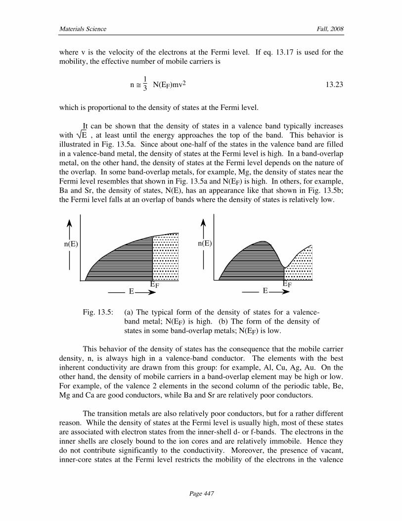
which is proportional to the density of states at the Fermi level. It can be shown that the density of states in a valence band typically increases with E , at least until the energy approaches the top of the band. This behavior is illustrated in Fig. 13.5a. Since about one-half of the states in the valence band are filled in a valence-band metal, the density of states at the Fermi level is high. In a band-overlap metal, on the other hand, the density of states at the Fermi level depends on the nature of the overlap. In some band-overlap metals, for example, Mg, the density of states near the Fermi level resembles that shown in Fig. 13.5a and N(EF) is high. In others, for example, Ba and Sr, the density of states, N(E), has an appearance like that shown in Fig. 13.5b; the Fermi level falls at an overlap of bands where the density of states is relatively low.
EEF
n(E)
EEF
n(E)
Fig. 13.5: (a) The typical form of the density of states for a valence-band metal; N(EF) is high. (b) The form of the density of states in some band-overlap metals; N(EF) is low.
This behavior of the density of states has the consequence that the mobile carrier density, n, is always high in a valence-band conductor. The elements with the best inherent conductivity are drawn from this group: for example, Al, Cu, Ag, Au. On the other hand, the density of mobile carriers in a band-overlap element may be high or low. For example, of the valence 2 elements in the second column of the periodic table, Be, Mg and Ca are good conductors, while Ba and Sr are relatively poor conductors. The transition metals are also relatively poor conductors, but for a rather different reason. While the density of states at the Fermi level is usually high, most of these states are associated with electron states from the inner-shell d- or f-bands. The electrons in the inner shells are closely bound to the ion cores and are relatively immobile. Hence they do not contribute significantly to the conductivity. Moreover, the presence of vacant, inner-core states at the Fermi level restricts the mobility of the electrons in the valence
Materials Science Fall, 2008
Page 448
states. Valence electrons become trapped in these empty states as they travel through the material, as illustrated in Fig. 13.6, so their mobility is relatively low.
Fig. 13.6: Possible path of a mobile valence electron through a transition metal, showing the periodic trapping by electron core states that restricts its mobility.
13.4 THE INFLUENCE OF TEMPERATURE AND PURITY The conductivity is determined both by the density of mobile electrons and by their mobility. The mobility is controlled by the frequency of collisions between the carriers and the scattering centers that are present in the lattice. The most important of these are lattice atoms that are displaced by lattice vibrations and impurity atoms that distort the local charge distribution. 13.4.1 The electron mean free path To analyze the influence of the scattering centers it is useful to rephrase the expression, 13.19, for the conductivity by replacing the relaxation time, †, by the mean free path between collisions, ´l¨:
† = ´l¨v 13.24
where v is the velocity of the mobile electrons, essentially equal to the velocity of an electron at the Fermi level. With this substitution,
ß = ne2
mv ´l¨ 13.25
When more than one scattering mechanism affects the mean free path, ´l¨, it is simpler to write an expression for the reciprocal, 1/´l¨. Let the electron make N collisions while moving through a distance, L. Let N1 of these collisions be with obstacles of type 1, while N2 are with obstacles of type 2. Then
Materials Science Fall, 2008
Page 449
N = L´l¨ = N1 + N2
= L
´l¨1 +
L´l¨2
13.26
where ´l¨i (i = 1 or 2) is the value the mean free path would have if only obstacles of type (i) were present. Hence the reciprocal mean free paths of the various obstacles sum to produce the reciprocal mean free path:
1
´l¨ = 1
´l¨1 +
1´l¨2
13.27
13.4.2 Matthiesen's Rule Since the resistivity, ®, is proportional to the reciprocal mean free path,
® = 1ß =
mvne2
1´l¨
= mvne2
1
´l¨1 +
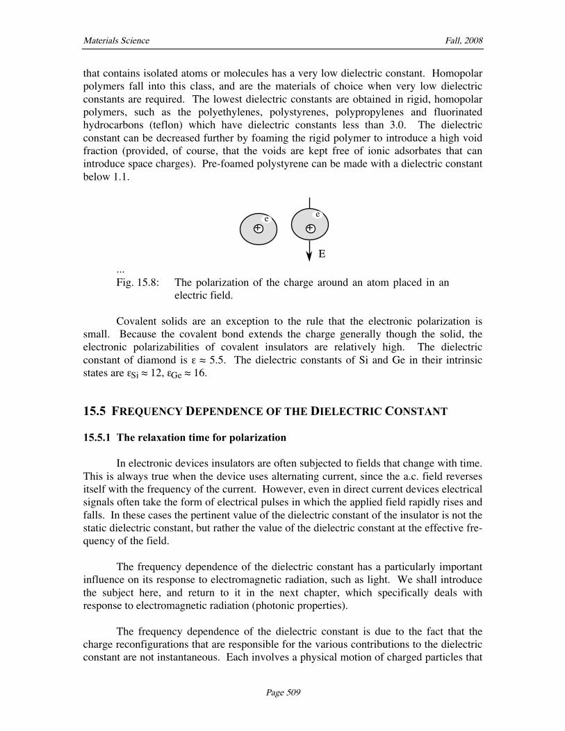
1´l¨2
13.28
the resistivity is the sum of contributions from the various obstacles that scatter electrons. Since the most important scattering mechanisms are foreign atoms and lattice vibrations, ® = ®i + ®T 13.29 where ®i is the contribution to the resistivity from scattering by impurities or solutes, and ®T is the contribution from lattice vibrations. Equation 13.29 is known as Matthiesen's Rule. Since the two contributions to the resistivity add, they can be analyzed separately. 13.4.3 The thermal resistivity of the crystal lattice First consider the part of the resistivity that is due to scattering from lattice vibra-tions. This mechanism determines the resistivity of a pure metal. The resistivity increases with the mean amplitude of the atom displacements that are caused by lattice vibrations. A quantum mechanical calculation of the effect gives the result that the lattice resistivity is proportional to T at moderate to high temperature, but vanishes with T5 as T approaches zero. Since the lattice vibrations are characterized by the Debye temperature, ŒD, we might expect that most pure metals would behave the same if both the resistivity and tem-
Materials Science Fall, 2008
Page 450
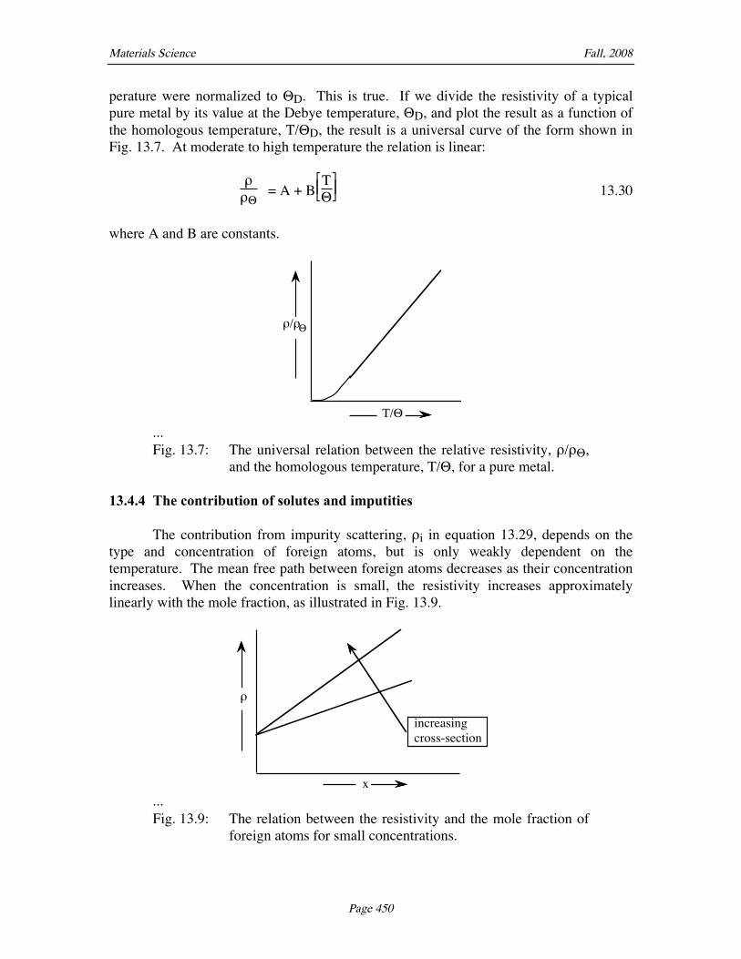
perature were normalized to ŒD. This is true. If we divide the resistivity of a typical pure metal by its value at the Debye temperature, ŒD, and plot the result as a function of the homologous temperature, T/ŒD, the result is a universal curve of the form shown in Fig. 13.7. At moderate to high temperature the relation is linear:
®
®Œ = A + B
T
Π13.30
where A and B are constants.
T/Œ
®/®Œ
...
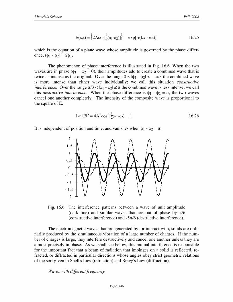
Fig. 13.7: The universal relation between the relative resistivity, ®/®Œ, and the homologous temperature, T/Œ, for a pure metal.
13.4.4 The contribution of solutes and imputities The contribution from impurity scattering, ®i in equation 13.29, depends on the type and concentration of foreign atoms, but is only weakly dependent on the temperature. The mean free path between foreign atoms decreases as their concentration increases. When the concentration is small, the resistivity increases approximately linearly with the mole fraction, as illustrated in Fig. 13.9.
®
x
increasing cross-section
...
Fig. 13.9: The relation between the resistivity and the mole fraction of foreign atoms for small concentrations.
Materials Science Fall, 2008
Page 451
The more strongly an impurity interacts with valence electrons the more it increases the resistivity at a given concentration. The scattering efficiency of an obstacle is associated with its scattering cross-section, which measures the probability that it will affect an electron that moves in its vicinity. The impurities that have the largest cross-sections in valence-band metals are usually transition elements, which not only distort the lattice, but also introduce empty core states that can trap electrons as illustrated in Fig. 13.6. The scattering cross-section of a non-transition element increases with its qualitative difference from the matrix atom. A significant size difference distorts the lattice; a significant difference in electron affinity produces a local charge at the defect. Other crystal defects, such as dislocations, grain boundaries and small clusters of atoms also increase the resistivity by scattering electrons. However, the distances between these defects are ordinarily so large that their contribution is negligible. The dislocation contribution can become significant when the metal is severely deformed to produce a very high dislocation density. As another example of defect-induced resistivity, the resistivity often increases significantly in the early stages of a precipitation reaction; when the precipitates are very small they scatter electrons efficiently. The resistivity drops as the precipitates grow; when the precipitates are larger the electrons penetrate into them and they behave more like bulk phases. 13.4.5 The total resistivity The two contributions to the resistivity result in a behavior like that shown in Fig. 13.9, which is a schematic plot of the resistivity of several samples of a metal with different purity. At very low temperature the impurity scattering dominates, so ® ~ ®i 13.31 and is nearly constant, while at moderate to high temperature, ® ~ ®0 + bT 13.32 where ®0 and b are constants. The constant, ®0, is the sum of the impurity contribution, ®i, and the integrated effect of the low-temperature contribution to the lattice resistivity, illustrated in Fig. 13.7. The impurity effect, ®i, is an essentially additive contribution to ®0, which has the consequence that the resistivity curves for samples of different purity are displaced from one another by an almost constant displacement which is proportional to the difference in solute content. The resistivity in the low-temperature limit is almost exactly equal to ®i, and, hence, is almost linearly proportional to the impurity concentration. Since the resistivity can be measured with very high accuracy, a measurement of the residual resistivity at low temperature is one of the best ways to assess the purity of nominally pure metals.
Materials Science Fall, 2008
Page 452
®
T
increasingpurity
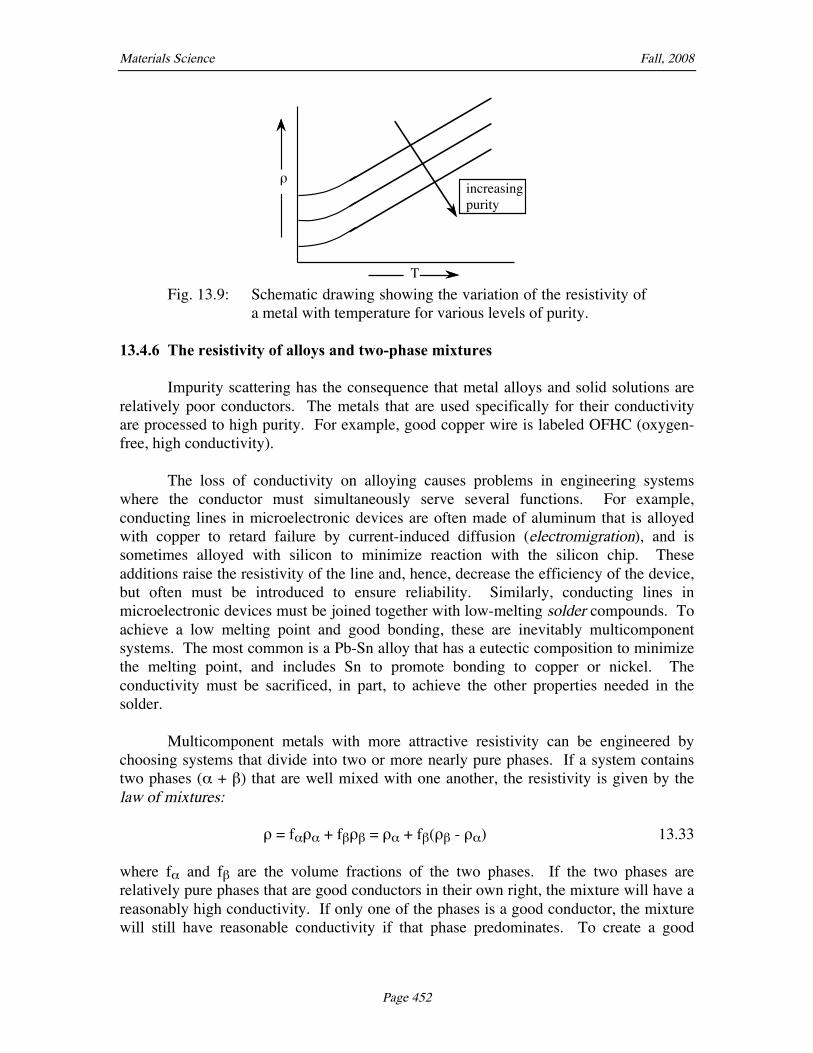
Fig. 13.9: Schematic drawing showing the variation of the resistivity of
a metal with temperature for various levels of purity. 13.4.6 The resistivity of alloys and two-phase mixtures Impurity scattering has the consequence that metal alloys and solid solutions are relatively poor conductors. The metals that are used specifically for their conductivity are processed to high purity. For example, good copper wire is labeled OFHC (oxygen-free, high conductivity). The loss of conductivity on alloying causes problems in engineering systems where the conductor must simultaneously serve several functions. For example, conducting lines in microelectronic devices are often made of aluminum that is alloyed with copper to retard failure by current-induced diffusion (electromigration), and is sometimes alloyed with silicon to minimize reaction with the silicon chip. These additions raise the resistivity of the line and, hence, decrease the efficiency of the device, but often must be introduced to ensure reliability. Similarly, conducting lines in microelectronic devices must be joined together with low-melting solder compounds. To achieve a low melting point and good bonding, these are inevitably multicomponent systems. The most common is a Pb-Sn alloy that has a eutectic composition to minimize the melting point, and includes Sn to promote bonding to copper or nickel. The conductivity must be sacrificed, in part, to achieve the other properties needed in the solder. Multicomponent metals with more attractive resistivity can be engineered by choosing systems that divide into two or more nearly pure phases. If a system contains two phases (å + ∫) that are well mixed with one another, the resistivity is given by the law of mixtures: ® = få®å + f∫®∫ = ®å + f∫(®∫ - ®å) 13.33 where få and f∫ are the volume fractions of the two phases. If the two phases are relatively pure phases that are good conductors in their own right, the mixture will have a reasonably high conductivity. If only one of the phases is a good conductor, the mixture will still have reasonable conductivity if that phase predominates. To create a good
Materials Science Fall, 2008
Page 453
conductor with a high strength it is best to strengthen the conductor with fine precipitates whose second element has almost no residual solubility in the matrix.
Materials Science Fall, 2008
Page 454
C h a p t e r 1 4 : S e m i c o n d u c t o r sC h a p t e r 1 4 : S e m i c o n d u c t o r s Mine is no callous shell, I have instant conductors all over me whether I pass or stop, They seize every object and lead it harmlessly through me. - Walt Whitman, "Song of Myself" 14.1 INTRODUCTION As suggested by their name, semiconductors are very poor conductors that have almost no engineering value as carriers of electricity. Nonetheless they are among the most important of engineering materials, and are the essential materials of the vast microelectronics industry. The primary reason that semiconductors are useful is not their conductivity, but their controllability. This controllability is peculiar to extrinsic semiconductors, which are semiconductors whose mobile carriers are liberated by electrically active solutes, which are the donor and acceptor solutes we discussed in Chapter 4. In an extrinsic semiconductor both the conductivity and the dominant carrier type (electrons or holes) can be precisely controlled by adjusting the type and concentration of active solutes. Semiconductors with different carrier types or very different carrier densities can be joined into composite semiconducting devices whose behavior depends on the microstructure of the composite and on the magnitude and distribution of the applied voltage. Semiconducting devices exploit the electronic behavior of junctions between materials that have different electrical characteristics. In this chapter we shall specifically consider two types of junctions that are particularly useful: the p-n junction that is basic to bipolar devices, such as junction diodes and bipolar transistors, and the metal-insulator-semiconductor (MIS) junction that is the essential element in charged coupled devices (CCD) and MOSFET devices (metal-oxide-semiconductor field effect transistors). Bipolar and MIS junction devices can be made to behave as resistors, rectifiers, power amplifiers, memory elements, logic gates, or any one of many other elements of electronic circuits. Since a composite semiconductors can be made with almost arbitrarily fine microstructures by selectively doping adjacent regions of a semiconductor crystal with appropriate solutes, complex electronic circuits can be "written" onto the surface of the crystal, or chip, and made to perform almost any function that is within the capability of a macroscopic circuit. A microelectronic device is essentially a composite material with a carefully engi-neered microstructure. The microstructural elements include semiconducting regions
Materials Science Fall, 2008
Page 455
with controlled composition, metallic conductors that connect semiconducting regions to one another and to the outside world, and insulating layers and films that separate the electrically active elements from one another. To achieve a modern level of miniaturization the dimensions of the microstructure must be reduced to at least the micron scale. Modern materials research addresses ways of shrinking them to nanometers. The complex microstructures of typical microelectronic devices are constructed by sequentially depositing materials on the surface of a semiconductor chip that is inhomogeneously doped with electrically active solutes. The materials processing techniques that are employed are among the most elaborate and precise yet developed. We shall briefly discuss some of their characteristic features. 14.2 INTRINSIC SEMICONDUCTORS 14.2.1 The band structure of an intrinsic semiconductor An intrinsic semiconductor has a band structure like that shown in Fig. 14.1. In the ground state (at T = 0) the valence band is just filled while the conduction band is just empty. Intrinsic semiconductors are distinguished from insulators by the magnitude of the band gap. In an intrinsic semiconductor the band gap, EG, is small enough that a modest concentration of free carriers is liberated by thermal activation across the band gap at finite temperature. An insulator has a larger band gap, and hence has a negligible concentration of free carriers at normal temperatures.
EFE EG
x
valence band
conduction band
E EG
x
EF
...
Fig. 14.1: The band structure of an intrinsic semiconductor. We discussed examples of intrinsic semiconductors in Chapter 2. The simplest elemental semiconductors are Group IVA elements, like Si and Ge, that have valence 4 and crystallize in the diamond cubic structure with four neighbors per atom; they can, hence, form saturated covalent bonds that lead to a filled valence band. The simplest compound semiconductors are III-V compounds like GaAs and II-VI compounds like CdTe that have an average valence of 4 and crystallize in the ∫-ZnS structure, so that they also form saturated covalent bonds. However, many other elemental solids and compounds are also semiconductors. These materials typically have an even number of
Materials Science Fall, 2008
Page 456
valence electrons per primitive cell of the Bravais lattice, and a small gap at the top of the highest filled valence band. Moreover, there are semiconductors that are not crystalline at all. Examples include amorphous silicon and selenium, which is even semiconducting when it is in the liquid state. The behavior of these materials is usually attributed to a strong short-range order. While these materials are amorphous in the sense that they have no long-range crystalline order, their short-range configurations, that is, the number, spacing and configuration of the more immediate neighbors of an atom, are believed to be very close to those in the crystalline form. 14.2.2 The free electron density in an intrinsic semiconductor At any temperature above absolute zero at least some of the electrons in a semiconductor occupy states in the conduction band, and are free to carry current. To a reasonable approximation the electron energy states themselves are not affected by the temperature, so the density of conduction electrons can be found by considering the most probable distribution of electrons over a fixed set of energy states. The probability that an electron fills a state of energy, E, at temperature, T, is given by the Fermi-Dirac distribution function,
P(E) = 1
1 + e 1kT(E-EF)
14.1
where EF is the Fermi energy, which satisfies the relation
P(EF) = 12 14.2
In the low temperature limit, T“0, the exponential factor in the denominator of equation 14.1 is infinite if E>EF and zero if E<EF. In this limit the states with energies above EF are empty while the states with energies below EF are filled; if the highest filled state is separated by a gap from the lowest empty state, the Fermi energy lies at the midpoint of the gap between them. In an intrinsic semiconductor the Fermi energy lies the center of the band gap, as shown in Fig. 14.1. The energy of a state at the bottom of the conduction band, Ec, is such that Ec - EF >> kT at ordinary temperatures. Hence the probability that a state in the conduction band with energy E > Ec is filled by an electron is given approximately by
P(E) ~ e - 1
kT(E-EF) (E - EF >> kT) 14.3
The number of conduction electrons per unit volume of crystal, n, is given by the integral
Materials Science Fall, 2008
Page 457
n = ⌡⌠
C P(E)N(E)dE
= ⌡⌠C N(E)e
- 1kT(E-EF)
dE 14.4
where N(E) is the density of states, the number of electron states with energies between E and E+dE in the conduction band, and the integral is taken over the conduction band. Since
e - 1
kT(E-EF) = e
- 1kT(Ec-EF)
e - 1
kT(E-Ec) 14.5
The number of conduction electrons can be written
n = e - 1
kT(Ec-EF)⌡⌠C N(E)e
- 1kT(E-Ec)
dE
= Nce - 1
kT(Ec-EF) 14.6
where Nc is an "effective number of states" for the conduction band,
Nc = ⌡⌠C N(E)e
- 1kT(E-Ec)
dE 14.7
Nc is of the order of N0, the number of atoms per unit volume, since each atom supplies excited electron states that appear in the conduction band. Nc depends on the temperature. It can be shown that Nc fi T3/2 14.8 However, the temperature dependence of the conduction electron density, n, is dominated by the exponential term in eq. 14.6. For purposes of understanding the thermal behavior of semiconductors we can usually neglect the temperature dependence of Nc and take it to be a constant of order N0. The electrons that are excited to the conduction band are free to conduct electricity, just like the free carriers in a metal. They contribute an electron conductivity, ße = neµe 14.9 where µe is the electron mobility, and is governed by the same scattering processes that determine the mobility of the conduction electrons in a metal.
Materials Science Fall, 2008
Page 458
14.2.3 Electron holes in intrinsic semiconductors Each electron that is thermally activated into the conduction band of an intrinsic semiconductor leaves behind an empty state (hole) in the valence band. The electrons in the valence band can use this empty state to move in response to an electric field. Effectively, the hole behaves as a mobile positive charge that is set in motion by an applied field. The simplest way to visualize electrical conductivity by holes is to consider an elemental semiconductor that has saturated covalent bonds in its ground state. The electron states in the bonds correspond to the electron states in the valence band. A hole in the valence band corresponds to an unfilled state in one of the bonds. As illustrated in Fig. 14.2, valence electrons can move by exchanging with this hole just as substitutional atoms on the sites of a crystal lattice diffuse by exchanging with lattice vacancies. When an electric field, E, is imposed electrons move in the direction opposite the field. Hence holes are transported with the field, as if they were particles of positive change.
SiSi
SiSi
Si
SiSi
SiSi
Si
...
Fig. 14.2: Covalent bonding in a tetrahedral configuration of silicon. If a hole appears, as shown at right, electrons can move by ex-changing with it.
Each diffusional step of the hole is a diffusional step of an electron in the opposite direction. A hole behaves as if it had positive charge, e. Since it is easier to visualize the motion of a single hole than the net motion of many electrons, we treat conduction in the valence band by considering that the valence band contains a population of positively charged holes that is equal to the density of empty electron states. The density of holes is designated by the symbol, p. To compute the density of holes we find the density of empty electron states in the valence band. The probability that an electron state that has energy, E, is empty at temperature, T, is
p(E) = 1 - P(E) = 1
1 + e 1kT(EF-E)
14.10
Equation 14.10 shows that the distribution of holes is also controlled by the Fermi energy and the temperature. When EF - E >> kT, as it is for states in the valence band of an in-trinsic semiconductor,
Materials Science Fall, 2008
Page 459
p(E) ~ e - 1
kT(EF-E) (EF - E >> kT) 14.11
Using an analysis identical to that which yields equation 14.6, the total density of holes, p, is
p = e - 1
kT(EF-EV)⌡⌠V N(E)e
- 1kT(EV-E)
dE
= Nve - 1
kT(EF-EV) 14.12
where EV is the energy at the top of the valence band and Nv is the effective number of states in the valence band,
NV = ⌡⌠V N(E)e
- 1kT(EV-E)
dE 14.13
The effective number of states, Nv, increases as T3/2 just as Nc does. However, for quali-tative purposes we can usually take it to be a constant of order N0. 14.2.4 The intrinsic carrier density and the Fermi energy The product of the electron and hole densities is
np = (NvNc)e - 1
kT(EC-EV)
= (NvNc)e -
EGkT = ni2 14.14
where EG = EC - EV 14.15 is the band gap energy, and ni is the intrinsic carrier density. Equation 14.15 is indepen-dent of EF, and depends only on the band gap and the effective numbers of states in the valence and conduction bands. Hence ni it is a property of a given semiconductor, and holds whether or not the semiconductor is intrinsic. In an intrinsic semiconductor,
n = p = ni = NvNc e -
EG2kT
Materials Science Fall, 2008
Page 460
~ N0e -
EG2kT 14.16
Since eq. 14.6 and 14.12 are equal for an intrinsic semiconductor, the Fermi energy is
EF = 12 [EV + EC] +
kT2 ln
Nv
Nc 14.17
The Fermi level in an intrinsic semiconductor falls at the midpoint of the band gap when T = 0, and remains near the midpoint of the band gap for all higher temperatures. 14.2.5 The conductivity of an intrinsic semiconductor
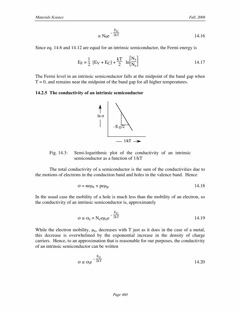
1/kT
ln ß
- E G/2
Fig. 14.3: Semi-logarithmic plot of the conductivity of an intrinsic semiconductor as a function of 1/kT
The total conductivity of a semiconductor is the sum of the conductivities due to the motions of electrons in the conduction band and holes in the valence band. Hence ß = neµe + peµp 14.18 In the usual case the mobility of a hole is much less than the mobility of an electron, so the conductivity of an intrinsic semiconductor is, approximately
ß ~ ße = Nceµee -
EG2kT 14.19
While the electron mobility, µe, decreases with T just as it does in the case of a metal, this decrease is overwhelmed by the exponential increase in the density of charge carriers. Hence, to an approximation that is reasonable for our purposes, the conductivity of an intrinsic semiconductor can be written
ß ~ ßie -
EG2kT 14.20
Materials Science Fall, 2008
Page 461
where ßi is a constant. It follows that a plot of the logarithm of ß against 1/kT yields a straight line with a negative slope, EG/2, as shown in Fig. 14.3. Fig. 14.3 holds to a very good approximation for almost all intrinsic semiconductors. 14.3 EXTRINSIC SEMICONDUCTORS 14.3.1 Types of extrinsic semiconductors An extrinsic semiconductor is a semiconductor whose charge carriers are primarily due to the ionization of defects in the crystal lattice. Ionization produces a density of extrinsic charge carriers that adds to the density of intrinsic charge carriers from intrinsic activation across the band gap. If the extrinsic carriers are electrons in the conduction band the defects are called donors and the extrinsic semiconductor is said to be n-type. If the extrinsic carriers are holes in the valence band the defects are acceptors and the semiconductor is p-type. The most common and most controllable of the electrically active defects are substitutional solute or impurity atoms whose valence differs from that of the lattice atoms they replace. We discussed these defects in Chapter 4. The case that is simplest to visualize is the replacement of an atom in an elemental Group IV semiconductor, such as silicon, by a Group III atom, such a boron, or a Group V atom, such as phosphorous. A substitutional element is always a donor when its valence exceeds that of the atom it replaces, and an acceptor when its valence is less. The Group V elements P, As, and Sb are donor elements in silicon, while the Group III elements B and Al are acceptors. The Group IV elements, like Si, are donors in GaAs when they substitute for Ga, but acceptors when they substitute for As. A donor replacement for As would be a Group VI element like S. An anti-site defect in a compound semiconductor like GaAs is an atom on the wrong site; As is a donor when it sits on a Ga site, Ga is an acceptor when it fills an As site. Crystal defects such a vacancies and dislocations are electrically active, and may act as donors or acceptors depending on the crystal and the precise defect type. 14.3.2 Donors: n-type semiconductors The prototypic example of a donor site is the substitution of silicon by phospho-rous, which is illustrated in Fig. 14.4. Phosphorous has five valence electrons. Four of these are needed to saturate Si-like covalent bonds to each of the four neighbors. The fifth is left over, and must fill an excited state in the local bonding configuration. Since the ion core of phosphorous has a charge of +5, as opposed to the charge +4 on the silicon ion cores, the excited electron is bound to phosphorous and, in its ground state, moves in a local orbital around it. However, because the electron is in an excited orbital, and is partly screened from the phosphorous nucleus by the other bonding electrons, this binding is relatively weak. Only a small excitation energy, the ionization energy of the phosphorous defect, is needed to separate the excited electron from the phosphorous core
Materials Science Fall, 2008
Page 462
and set if free to move through the conduction band of the semiconductor. Phosphorous acts as a donor that can liberate electrons into the conduction band of the semiconductor.
SiSi
SiSi
Si
SiSi
SiSi
P
e
Fig. 14.4: The local bonding configuration in elemental silicon, as dis-turbed by the substitution of an atom of phosphorous.
The band structure of an extrinsic semiconductor that contains a distribution of donor sites is illustrated in Fig. 14.5. Assuming that the donors are separated widely enough that they do not interact with one another, each donor site introduces a spatially localized electron state within the band gap. These have an energy, ED, such that ÎED, the energy difference between the donor level and the bottom of the conduction band, is the ionization energy of the donor electron. Since the donor states are relatively close to the conduction band, their electrons are thermally excited into the conduction band to provide a distribution of free electrons when the temperature is still so low that the intrinsic electron density is negligible. Hence there is a range of temperatures for which essentially all of the charge carriers in the semiconductor are electrons provided by the donor sites, and the semiconductor behaves as an n-type extrinsic semiconductor.
Conduction band
Valence band
ÎEGE
x
donor levels
} ÎED
Fig. 14.5: Donor levels within the band gap of an n-type extrinsic semi-conductor.
14.3.3 Acceptors: p-type semiconductors A prototypic example of an acceptor defect is the substitution of silicon by boron, which is illustrated in Fig. 14.6. Since boron has valence 3, its valence electrons are in-sufficient to saturate the local bonding states. One of the electron states is left vacant.
Materials Science Fall, 2008
Page 463
The vacant state is a hole in the bonding configuration. Since the charge on the boron ion core is +3 rather than +4, the hole is bound to the boron atom. However, it requires only a relatively small ionization energy for a bonding electron from the surrounding silicon to move into the vacant site, liberating the hole into the valence band of the crystal. Boron is, hence, an acceptor defect in silicon.
SiSi
SiSi
Si
SiSi
SiSi
B
Fig. 14.6: The substitution of silicon by boron produces a hole in the local bonding configuration.
When an electron moves from the valence band to fill a hole its energy increases to a level slightly within the band gap. It cannot return to the valence band unless it recombines with a hole in an adjacent position of the crystal. As a consequence, the electron occupies a localized state that lies slightly within the valence band. The band structure of an extrinsic semiconductor that contains a distribution of acceptor sites is illustrated in Fig. 14.7. If the acceptors do not interact, each introduces a spatially localized electron state within the band gap. The acceptor energy is EA. ÎEA, the energy difference between the acceptor level and the top of the valence band, is the ionization energy of the acceptor site. Since ÎEA << EG, there is a range of temperatures for which essentially all of the charge carriers in the semiconductor are holes provided by the acceptor sites, and the semiconductor behaves as an p-type extrinsic semiconductor.
Conduction band
Valence band
ÎEGE
x
acceptor levels
} ÎEA
Fig. 14.7: Schematic band diagram of a semiconductor doped with acceptors showing the localized acceptor levels.
Materials Science Fall, 2008
Page 464
14.3.4 Carrier density in an n-type semiconductor The Fermi energy To calculate the number of carriers in an extrinsic semiconductor it is sufficient to know the value of Fermi energy. Since equations 14.6, 14.12 and 14.17 hold irrespective of the source of the carriers, the relations
n = Nce - 1
kT(Ec-EF) 14.21
p = Nve - 1
kT(EF-EV) 14.22
np = [NcNv] e -
EGkT 14.23
govern the density of free carriers in extrinsic semiconductors as well as intrinsic ones. Extrinsic semiconductors differ from intrinsic semiconductors in the value of the Fermi energy. To find the Fermi energy and gain some insight into the temperature variation of the free carrier density in an extrinsic semiconductor, consider the case of an n-type semiconductor that has a density, ND, of donors per unit volume. The free electrons in the conduction band of the semiconductor have two sources, ionization of the donor sites and intrinsic activation across the band gap. If we write the number of ionized donors as ND+, then the density of conduction electrons, n, is given by n = ND+ + p 14.24 where p is the density of holes in the valence band. Equations 14.23 and 14.24 determine n and p in terms of the Fermi energy. The number of ionized donors is more difficult to calculate. Assuming that the donor has one excess electron, this electron can reside in ei-ther of two states (one of each spin). Since both donor states cannot be filled without raising the energy of the donor by, effectively, ionizing it negatively, almost all donors are either neutral (one of the electron states full) or ionized (both electron states empty). The probability that both states are empty is P(0) = [1 - P(E)]2 14.25 where P(E) is the Fermi-Dirac distribution function, eq. 14.1. The probability that one state is full is P(1) = 2P(E)[1-P(E)] 14.26
Materials Science Fall, 2008
Page 465
where the factor, 2, comes from the fact that either state can be filled. It follows that the fraction of ionized donors is given by
ND+
ND =
[1 - P(E)]2
[1 - P(E)]2 + 2P(E)[1 - P(E)]
=
1 + 2
P(E)
1-P(E)-1
=
1 + 2e - 1
kT(ED-EF) -1 14.27
Substituting this equation along with 14.21 and 14.22 into 14.24 gives the result:
Nce - 1
kT(Ec-EF) = ND
1 + 2e - 1
kT(ED-EF) -1 + Nve
- 1kT(EF-EV)
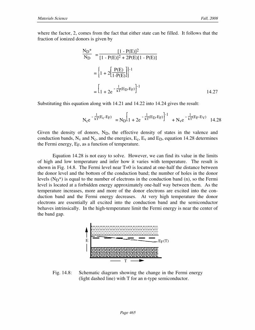
14.28 Given the density of donors, ND, the effective density of states in the valence and conduction bands, Nv and Nc, and the energies, Ec, Ev and ED, equation 14.28 determines the Fermi energy, EF, as a function of temperature. Equation 14.28 is not easy to solve. However, we can find its value in the limits of high and low temperature and infer how it varies with temperature. The result is shown in Fig. 14.8. The Fermi level near T=0 is located at one-half the distance between the donor level and the bottom of the conduction band; the number of holes in the donor levels (ND+) is equal to the number of electrons in the conduction band (n), so the Fermi level is located at a forbidden energy approximately one-half way between them. As the temperature increases, more and more of the donor electrons are excited into the con-duction band and the Fermi energy decreases. At very high temperature the donor electrons are essentially all excited into the conduction band and the semiconductor behaves intrinsically. In the high-temperature limit the Fermi energy is near the center of the band gap.
EFE
T
(T)
Fig. 14.8: Schematic diagram showing the change in the Fermi energy (light dashed line) with T for an n-type semiconductor.
Materials Science Fall, 2008
Page 466
The free electron density as a function of temperature To estimate the free electron density, first consider the low-temperature limit. When the temperature is very low the density of holes, p, is much less than the density of ionized donors, ND+. Moreover, ND+ is small, so the Fermi energy must be above ED. Assuming EF - ED >> kT we have
EF = 12 [Ec + ED] +
kT2 ln
ND
2Nc 14.29
Hence in the limit, T “ 0, EF lies midway between the donor level and the bottom of the conduction band. The number of carriers in the conduction band, n, is given approxi-mately by
n ~ NDe - 1
kT(E-EF) =
NcND2 e
- ÎED2kT 14.30
The number of carriers increases with the square root of the donor density and increases exponentially with the temperature.
ln(n)
1/kT
intrinsic
saturationextrinsic
ÎED/2kT
EG2kT
higher ND
Fig. 14.9: The temperature variation of the density of carriers, n, in the conduction band of an n-type semiconductor, for several val-ues of the donor density, ND.
As the temperature rises, the number of ionized donors increases, and the Fermi energy drops below the donor level. If ÎED, the distance from the donor level to the bottom of the conduction band, is small, and is also a small fraction of the total energy gap, ÎEG, then there is a range of temperature for which Ec - EF > ED - EF >> kT and EF - EV >> kT. Then n « ND 14.31
Materials Science Fall, 2008
Page 467
and the extrinsic semiconductor is said to be saturated. Extrinsic semiconductors are often designed so that they saturate near room temperature, so the carrier density in service is easy to predict. At all temperatures,
p = ni2
n 14.32
where ni2 is given by equation 14.22. When the temperature becomes great enough that ni2 > ND2, that is, when T is such that
ND2 < [NcNv] e -
EGkT 14.33
the donor density is no longer sufficient to supply the electron concentration in the conduction band. Intrinsic activation across the band gap becomes the primary source of conduction electrons. The Fermi level falls to a position near the midpoint of the band gap and remains there at all higher temperatures; the conduction electron density at high temperature is given by the intrinsic value
n ~ NcNv e -
EG2kT 14.34
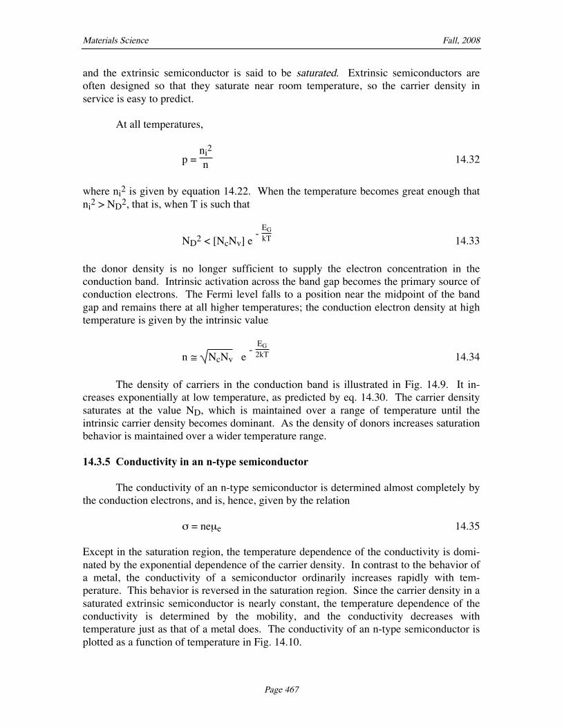
The density of carriers in the conduction band is illustrated in Fig. 14.9. It in-creases exponentially at low temperature, as predicted by eq. 14.30. The carrier density saturates at the value ND, which is maintained over a range of temperature until the intrinsic carrier density becomes dominant. As the density of donors increases saturation behavior is maintained over a wider temperature range. 14.3.5 Conductivity in an n-type semiconductor The conductivity of an n-type semiconductor is determined almost completely by the conduction electrons, and is, hence, given by the relation ß = neµe 14.35 Except in the saturation region, the temperature dependence of the conductivity is domi-nated by the exponential dependence of the carrier density. In contrast to the behavior of a metal, the conductivity of a semiconductor ordinarily increases rapidly with tem-perature. This behavior is reversed in the saturation region. Since the carrier density in a saturated extrinsic semiconductor is nearly constant, the temperature dependence of the conductivity is determined by the mobility, and the conductivity decreases with temperature just as that of a metal does. The conductivity of an n-type semiconductor is plotted as a function of temperature in Fig. 14.10.
Materials Science Fall, 2008
Page 468
ln(ß)
1/kT
intrinsic
saturationextrinsic
ÎED/2kT
EG2kT
higher ND
...
Fig. 14.10: The conductivity of an extrinsic semiconductor as a function of temperature and donor density. Note the decrease in ß in the saturation region, whose magnitude has been exaggerated for clarity.
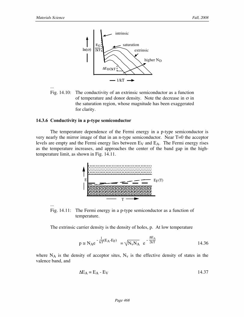
14.3.6 Conductivity in a p-type semiconductor The temperature dependence of the Fermi energy in a p-type semiconductor is very nearly the mirror image of that in an n-type semiconductor. Near T=0 the acceptor levels are empty and the Fermi energy lies between EV and EA. The Fermi energy rises as the temperature increases, and approaches the center of the band gap in the high-temperature limit, as shown in Fig. 14.11.
EFE
T
(T)
...
Fig. 14.11: The Fermi energy in a p-type semiconductor as a function of temperature.
The extrinsic carrier density is the density of holes, p. At low temperature
p ~ NAe - 1
kT(EA-EF) = NvNA e
- ÎEA2kT 14.36
where NA is the density of acceptor sites, Nv is the effective density of states in the valence band, and ÎEA = EA - EV 14.37
Materials Science Fall, 2008
Page 469
is the energy difference between the acceptor energy and the top of the valence band. At intermediate temperature the carrier density saturates (assuming NA is large enough), and p ~ NA 14.38 At high temperature the semiconductor becomes extrinsic: n = p = ni 14.39 Hence the carrier density varies with the temperature as shown in Fig. 14.9, replacing ND by NA, and the conductivity has the behavior shown in Fig. 14.10. Note, however, that the type of carrier that dominates the conductivity is different in the high- and low-temperature regions of a p-type semiconductor. At low temperature where the extrinsic carriers govern the conductivity, the current is carried predominantly by holes because of their greater number. At high temperature where intrinsic carriers predominate, the current is carried predominantly by electrons because of their greater mobility. 14.3.7 Compensation between active sites A real semiconductor inevitably contains at least some defects of both donor and acceptor type, if only because the native impurities in the semiconductor include defects of both types. The defects compensate one another, as shown in Fig. 14.12. Electrons from filled donor levels can decrease their energy by ionizing acceptor states.
Conduction band
Valence band
donor levels
acceptor levelsE
x
Fig. 14.12: Compensation of extrinsic defects by charge transfer from defects of the opposite type.
The compensation of defects has the consequence that the type and conductivity of the semiconductor is determined by the excess defects. For example, if there are ND donors per unit volume and NA < ND acceptors, the semiconductor is n-type, and its be-havior is approximately the same as that of an n-type semiconductor with a defect density ND' = ND - NA. Because of compensation, it is possible to change the type of an extrinsic semiconductor by adding an excess density of defects of the opposite type. The effective defect density is the excess density of the more populous defects.
Materials Science Fall, 2008
Page 470
14.3.8 Degenerate semiconductors Throughout this discussion of extrinsic semiconducting behavior we have assumed that the concentration of defects is small enough that the defects do not interact with one another. This requires that the defects be separated by at least several atom spacings so that their charges are effectively screened from one another and their excited electron or hole orbitals do not overlap. When the concentration of defects becomes so high that the defects begin to affect one another the defect states join together to form a impurity band of electron or hole states that is continuous through the crystal, and ordinarily overlaps the conduction or valence band. When this happens the semiconductor is said to be degenerate. Since the defect states in a degenerate semiconductor are not localized, a degenerate semiconductor is a metallic conductor, albeit a rather poor one. The degenerate limit of an extrinsic semiconductor has two important engineering consequences. First, it requires that extrinsic semiconductors be very pure. If only one percent of the crystal sites are filled by active solutes, their mean separation is only a bit over three atom spacings. To maintain an inter-defect distance of ten atom spacings or more the total defect concentration must not exceed one part in a thousand. Hence the crystals that are used as semiconductors must be grown or processed to exceptional purity. Second, the degenerate limit can be exploited to introduce metallic conduction into a semiconducting device. It is sometimes useful to introduce a region of metallic conductivity into a semiconductor to form a conducting line between different devices in the same crystal, as an alternative to depositing a metal film on its surface. While the conductivity in the degenerate region is not very high, it may nonetheless be satisfactory if the conductor is very small, and it is often very easy to manufacture by locally "over-doping" the semiconductor with active impurities. Such conductors are used widely in microelectronic devices. 14.3.9 Carrier lifetime Electrons and holes in semiconductors exist in a dynamic equilibrium in which they are constantly created by ionization processes and destroyed by recombination with one another. Hence each carrier has a finite lifetime. The carrier lifetime is particularly important in devices, such as the bipolar transistors we shall discuss below, in which an important part of the current is carried by minority carriers, such as electrons injected into a p-type extrinsic region. For a device like this to operate properly the minority carriers must survive for a sufficiently long time before being destroyed by recombination. There are two recombination processes that limit carrier life: direct recombination between electrons and holes, and impurity-assisted recombination, in which a majority carrier recombines with a minority carrier that is temporarily trapped at an impurity.
Materials Science Fall, 2008
Page 471
The probability of direct recombination depends on the basic nature of the semiconductor. In some semiconductors, such as GaAs, the electrons at the bottom of the conduction band can combine with holes at the top of the valence band by simple collision, and direct recombination is a common process. In other common semiconductors, such as Si and Ge, this kind of recombination is not possible. The nature of the energy bands is such that the electrons at the bottom of the conduction band have a momentum that differs from that of the holes at the top of the valence band. Since momentum is conserved in a collision, these carriers cannot simply combine. They can only annihilate one another in a process in which a phonon of lattice vibration is liberated or absorbed to conserve the momentum. Such semiconductors are called indirect-gap semiconductors. Electron-hole recombinations in indirect-gap semiconductors require three-body collisions that are much less probable than the two-body collisions that cause recombination in direct-gap semiconductors, like GaAs, where the momenta of the least energetic electrons and holes are the same. For this reason the minority carrier lifetime in pure Si and Ge is much longer than that in GaAs, and Si and Ge are easier to use in devices that depend on conduction by minority carriers, such a bipolar transistors. Carrier recombinations in an indirect-gap semiconductor happen primarily at electrically active defects. Carriers can be trapped in the local states of these defects and held there until a carrier of the opposite type arrives to recombine through what is essentially an inelastic collision. This is another reason why the semiconductors that are used in devices such as bipolar transistors must be exceptionally pure and perfect. Even impurities or lattice defects that do not introduce active donor or acceptor sites (particularly including the deep level defects whose localized states lie near the center of the band gap) can poison a device that requires minority carrier conduction by decreasing the carrier lifetime. 14.4 THE N-P JUNCTION 14.4.1 The Fermi energy at a heterogeneous junction The interesting properties of junctions between semiconductors that have different electronic characteristics derive from the behavior of the electron energy bands near the junction. To understand this behavior, first consider the change in the band structure that occurs when n-type and p-type regions are adjacent to one another in the same crystal. Let the junction be created in an imaginary operation in which the crystal is sliced apart along the plane that will eventually be the plane of the junction, one half is doped to become n-type, the other is doped to become p-type and the two are joined together again. Before the two regions are separated they have the same band structure and the same Fermi level, which lies at the mid-point of the band gap since the pure crystal is in-trinsic. The situation after the two halves are doped is shown in Fig. 14.13. The left-hand side is doped n-type and has a Fermi level near the top of the band gap. The right-
Materials Science Fall, 2008
Page 472
hand side is doped p-type and has its Fermi level neat the bottom of the band gap. In both cases the electrons in the conduction band (and holes in the valence band) move freely through the half-crystal because their states are delocalized.
E
x
E
x
EFEF
Fig. 14.13: Separated regions of the same semiconductor are doped n-type (left) and p-type (right). The Fermi energies are shown.
Now let the two doped regions be joined. Fig. 14.14 illustrates the state of the junction before any relaxation has occurred. Since the two regions are part of the same crystal, their energy bands join one another and the electrons and holes are able to move freely across the junction. First consider the conduction band. Because the Fermi level in the n-type region is above that in the p-type region, the density of conduction electrons is much higher in the n-type region. The number of electrons that move across the interface into the p-type region per unit time (the electron current in the positive direction) is proportional to the electron density in the n-type region, and is, hence,
j+ = Nce- 1
kT(EC-EnF)
14.40 where En
F is the Fermi energy in the n-type material and A is a constant of proportionality.
E
x
EF
e e e e e e e
Fig. 14.14: The band structure instantaneously after the n- and p-type re-gions in Fig. 14.13 are joined together. The Fermi energy is discontinuous at the junction, and electrons can combine with holes there, as indicated by the arrow in the figure.
The reverse current into the n-type region is proportional to the electron density in the p-type material, and is, hence,
Materials Science Fall, 2008
Page 473
j- = Nce- 1
kT(EC-EpF)
14.41 where Ep
F is the Fermi energy in the p-type region. Comparing the two equations shows that there is a net flux of electrons from the n-type region to the p-type region, which causes a net accumulation of electrons in the p-type material. A similar analysis of the hole concentrations in the two regions shows that there is a net flux of holes into the n-type region which is equal in magnitude to the net flux of electrons into the p-type region. There is, hence, a net accumulation of electrons (negative charge) in the p-type region and a net accumulation of holes (positive charge) in the n-type region. Since the positive and negative charges attract they remain near the interface and create the double layer of charge shown in Fig. 14.15.
n p++++
+++
-
--
--
--
Fig. 14.15: The double-layer of charge at the interface between n- and p-type regions of semiconductor.
The separation of charge at the interface creates a potential difference between the two regions. The potential difference changes the relative values of the electron energies in the regions on the two sides of the interface, and eventually leads to an equilibrium in which the Fermi energy is the same everywhere. To understand this behavior, consider an electron that is in a state with energy, E, in a semiconductor that is grounded so that its potential is zero. If the potential is changed to the new value, V, the energy of the electron state changes to E(V) = E + qV = E - eV 14.42 where q is the electron charge, and e = |q| is its magnitude. All of the electron states in a region with a given value of the potential, V, are shifted by the same amount. Since the Fermi energy depends only on the relative positions of the electron states, the Fermi energy is also shifted to EF(V) = EF + qV = EF - eV 14.43 where EF is the value of the Fermi energy when the potential is zero. Referring back to Fig. 14.15, the potential of the n-type material in the p-n junction, where positive charge accumulates, is raised relative to that of the p-type material. The energy levels (including the Fermi energy) in the n-type material are, therefore, lowered relative to those in the p-type material. The charge transfer continues and the potential difference increases until the spontaneous current across the interface
Materials Science Fall, 2008
Page 474
falls to zero. This happens when the energy levels have changed so that the Fermi level is the same on both sides of the interface. The band structure at equilibrium is like that shown in Fig. 14.16. The potential on the n-side of the interface is raised with respect to that on the p-side by the amount
e΃º = EnF - E
pF = Ep
c - Enc 14.44
where ΃º is the contact potential at the junction, En
F and EpF are the Fermi energies on
the two sides of the junction before contact is established, and Epc and En
c are the energies at the bottom of the conduction band on the p- and n-sides of the junction after equilibrium is reached. To see that this situation corresponds to zero net current across the interface rec-ognize that each electron state on the n-side of the interface experiences the potential drop, ΃º, on crossing the interface, that is, its energy is raised by the amount, - e΃º. The net flux of electrons toward the surface from the n-side is nn
e ev, where nne is the
conduction electron density on the n-side and v is the electron velocity toward the interface (in the region beyond the double-layer, v is not affected by the presence of the junction). Of the electrons that approach the interface, a fraction exp(-e΃º/kT) pass the potential barrier and travel into the p-region. Hence the net electron flux in the positive direction is
j+e = (nne ev)exp
-e΃º
kT = (Ncev)exp
- (En
c - EF)kT exp
-e΃º
kT 14.45
where we have used eq. 14.6. The reverse electron current from the p-side is
j-e = (nne ev) = (Ncev)exp
- (Ep
c - EF)kT 14.46
Equating the two shows that the net electron flux vanishes when EF is the same on both sides of the interface and the potential difference, V, satisfies eq, 14.44.
E EF
x
e e e e e e
Fig. 14.16: An n-p junction at equilibrium showing the shift in the level of the bands and the continuity of the Fermi energy.
Materials Science Fall, 2008
Page 475
The same analysis holds for the hole density in the valence band. Hence the net charge transport across the interface falls to zero. At equilibrium the Fermi energy is the same on both sides of the junction, and the contact potential is equal to the difference be-tween the original values of the Fermi energies. 14.4.2 Response to an Impressed Potential Now let an external potential be impressed across the junction, for example, by connecting the two ends of the semiconductor to the terminals of a battery, as shown in Fig. 14.17. In typical situations there is enough conductivity in each of the homogeneous regions of the semiconductor to achieve a constant potential, so the potential difference between the two ends of the semiconductor is concentrated at the junction. The im-pressed potential raises the potential of the p-type region by V relative to that in the n-type region. If V is positive, the junction is said to have forward bias; if V is negative, the junction is said to have negative bias. In either case the energy levels in the p-type region are shifted relative to those in the n-type region by the additional amount - eV, where V is the external potential and e is the electron charge. The shift is illustrated for the case of forward bias in Fig. 14.17, and for reverse bias in Fig. 14.18.
n p++++
+++
-
--
--
-- +-
E EF
x
e e e e e e
}eV
e
Fig. 14.17: Schematic and band diagram for an n-p junction under forward bias.
The electron current in the positive direction can be found by the same analysis that was used to obtain eq. 14.45, and is
j+e = j0e e eVkT 14.47
where j0e is the equilibrium flux (given by eq. 14.45 or 14.46). The electron flux in the negative direction remains at the value, j0e . Hence the net flux of electrons across the junction is
Materials Science Fall, 2008
Page 476
je = j+e - j-e = j0e
e eVkT - 1 14.48
A similar analysis shows that the net flux of holes is equal, but in the opposite direction. Since the holes transport positive charge, the net flux of charge carried by the electrons and the holes is identical, so the total current is twice the current due to the electrons. By convention, the flow of current is opposite to the flow of electrons. Hence the current density, j, in the positive direction is
j = -2je = 2j0e
1 - eeVkT 14.49
If V is positive, that is, if the junction has forward bias, then the current is in the negative direction and its density increases with the voltage, becoming nearly exponential when eV is significantly greater than kT. If V is negative, which corresponds to reverse bias, the current is in the positive direction, but rapidly asymptotes at the value j = 2j0e 14.50 when e|V| becomes greater than kT.
EFE
x
e e e e e eeV{
e
n p++++
+++
-
--
--
--+ -
Fig. 14.18: Schematic and band diagram for an n-p junction under reverse bias.
The current, I, is obtained from the current density by multiplying by the cross-sectional area of the semiconductor. The dependence of the current on the voltage is shown schematically in Fig. 14.19. For simplicity, we have plotted - I against V to show the electron current across the junction. [Note that the voltage, V, is the voltage that is externally applied. The contact potential, ΃º, is not included in V.]
Materials Science Fall, 2008
Page 477
- I
V
Fig. 14.19: The current-voltage characteristic of an n-p junction.
It is useful to spend a moment considering the physical source of the current under forward and reverse bias. Under forward bias the net current is due to an excess flux of the majority carriers: electrons from the conduction band of the n-type conductor and holes from the valence band of the p-type conductor. The flow is indicated by the arrows in Fig. 14.17. As the voltage increases, an exponentially increasing fraction of the electrons in the conduction band of the n-type material (holes in the valence band of the p-type material) is free to move across the interface. Hence the current increases exponentially. Shortly after the electrons move across the interface they annihilate with holes in the valence band of the p-type material. The holes that move into the n-type material are, similarly, annihilated by electrons from the conduction band. Hence the equilibrium charge densities are preserved and a steady-state current results. Under reverse bias, on the other hand, the current is due to an excess flux of the minority carriers: the electrons in the p-type material and the holes in the n-type material. The flow is indicated by the arrows in Fig. 14.18. Since the current cannot be greater than 2j0e , its value when j+ vanishes, which is necessarily small because of the low density of minority carriers, it asymptotes to a small upper limit. 14.5 THE N-P-N JUNCTION The n-p-n junction (or, equivalently, the p-n-p junction) is the basis of the bipolar transistor and, hence, of a large variety of important electronic devices. The three elements of an n-p-n junction are called, respectively, the emitter, the base, and the collector. The terminology is such that under an applied voltage electrons move from the emitter to the collector; the potential is hence relatively positive at the collector. For reasons that will be discussed below the base is made relatively thin. The band diagram for an n-p-n junction in the absence of an applied voltage is also shown in Fig. 14.20. At equilibrium the Fermi energy is constant through the device. 14.5.1 Voltage applied at the collector Suppose a voltage, ÎV > kT, is imposed across the n-p-n junction as shown in Fig. 14.21. Let VE, VB, and VC be the voltages in the emitter, base, and collector, respectively. The voltage drop across the device is
Materials Science Fall, 2008
Page 478
ÎV = VC - VE 14.51 where VC > VE. The potential in the base, VB, initially has some intermediate value. The potential drop is such that the emitter-base junction is in forward bias while the base-collector junction is in negative bias. Hence current flows relatively easily across the emitter-base junction, but only a small current flows across the base-collector junction into the collector. The consequence is that the potential difference between the emitter and base is rapidly lost due to charge transfer. After a short time VB«VE and ÎV is concentrated at the base-collector junction. The n-p-n junction behaves very much as if it were a simple p-n junction in reverse bias.
e e e e e e e e e e e e
x
E
n p n
EF
Fig. 14.20: Band diagram for an n-p-n junction showing the constant value of the Fermi energy.
Note that the n-p-n junction is two junctions in series; one of them is always in re-verse bias when a voltage is imposed across terminals placed at the two ends. It therefore responds as if it were a p-n junction in reverse bias for either sign of the potential change across the device.
n p n +-
e e e e e e
e e e e e eE EF
e
x
Fig. 14.21: Schematic band diagram for an n-p-n bipolar device subject to an external voltage.
Materials Science Fall, 2008
Page 479
14.5.2 Voltage applied at the base
n p n +-
e e e e e e
e e e e e eE
EF
e
x
+
Fig. 14.22: Band diagram of a bipolar n-p-n device in which the emitter, base and collector potentials are separately controlled. Electrons flow from emitter to base, and are swept to the col-lector.
Now suppose that a third terminal is connected directly to the base of the n-p-n device, as shown in Fig. 14.22, so that the potential at the base can be controlled indepen-dently. Let the potentials be controlled so that VC > VB > VE. The potential difference at the emitter-base junction sets it in forward bias so electrons flow into the base and holes flow out of it into the emitter. Since the voltage difference VB - VE is maintained, the current does not disappear with time. Continuity requires that it be maintained by a combination of current from the collector and current from the device that maintains the voltage, VB. Since the emitter-base junction is in forward bias the current into the base increases exponentially with the voltage difference, (VB - VE). At steady state the electrons that are injected into the base from the emitter combine with excess holes in the p-type base to maintain equilibrium. However, the region near the emitter-base junction is depleted in holes, since there are swept into the emitter. Hence excess electrons move freely for some distance into the base. If the base is relatively thin, these excess electrons reach the neighborhood of the base-collector interface, where they are swept into the collector by the potential difference (VC - VB). This process is energetically favorable since it provides the maximum decrease in the energy of the electrons. Hence when the base is thin and the difference (VC - VB) is significantly greater than kT (which requires only a small fraction of a volt at room temperature) almost all of the electrons that enter the base are swept into the collector. The collector current is then nearly equal to the current at the emitter-base junction, and increases exponentially with the voltage difference, (VB - VE). It follows that when the base is thin and its potential is controlled independently at a value intermediate between VC and VE, an n-p-n junction can be made to behave very
Materials Science Fall, 2008
Page 480
much like an n-p junction in forward bias. The current in the collector increases exponentially with the potential difference between the emitter and the base. 14.5.3 Two applications of the bipolar transistor A bipolar transistor, such as the n-p-n device described above, can be set up in a great many alternate ways by controlling the currents or voltages of the three contacts that lead to the emitter, base, and collector. Two possible applications are its use as a memory element and as a power amplifier. First consider how a transistor might be used as a memory element. We found above that if the voltage applied to the base is zero (or negative) then the transistor behaves like a single junction in reverse bias, while if a positive voltage is applied to the base it behaves like a junction in forward bias. Hence by applying a voltage at the collector and reading the resulting current one can easily tell whether the base voltage is positive. Let a positive voltage indicate the number (1) while a null voltage indicates (0). A binary number can be stored by setting the voltage at the base and read by measuring the current induced by a voltage at the collector. Hence the transistor can act as a memory element. Second, consider how a transistor can behave as a power amplifier, which is one of its more important technological applications. Let an n-p-n transistor be set up as shown in Fig. 8.12, but with a much larger potential difference imposed between the collector and the base. The current through the n-p-n transistor to the base is fixed by the potential difference between the emitter and the base. The power transmitted across that interface is P1 = I(VB - VE) 14.52 If the potential at the collector is strongly positive with respect to the base then the current to the collector is nearly the same. However, the power is amplified, since P2 = I(VC - VB) >> P1 14.53 Many other useful applications are possible and common. 14.6 METAL-INSULATOR-SEMICONDUCTOR JUNCTIONS The metal-insulator-semiconductor junction is the basis for an alternative set of microelectronic devices that are widely used in modern electronics. Common examples are the charge-coupled devices (CCD) that are used in semiconductor memories and photodetectors, and the metal-oxide-semiconductor field effect transistors (MOSFET) that are the most common form of transistor in advanced microelectronic devices.
Materials Science Fall, 2008
Page 481
The property of the metal-insulator-semiconductor junction that is exploited in these devices is the ability to invert the type of the semiconductor by adjusting the voltage applied to the metal. Fig. 14.23 illustrates the junction in its normal and inverted states. For the sake of an example we have assumed that the semiconductor is p-type.
n
metaloxide
+ + + +++ ++
V+
p-
p
metaloxide
p
...
Fig. 14.23: A metal-oxide-semiconductor junction before and after the imposition of a positive potential at the metal terminal. The depletion layer is labeled p-.
The inversion of a p-type semiconductor is accomplished by applying a positive voltage to the metal lead. This induces a distribution of positive charge at the metal-oxide interface, which acts like one plate of a capacitor, and lowers the potential at the oxide-semiconductor interface. If the semiconductor were a metal, then the potential at the oxide interface would result in a flow of electrons to establish a negative charge distribution at the interface; the device would be a parallel plate capacitor. However, since the semiconductor is p-type the electrons are the minority carriers, and their number is small. It is not possible to accumulate enough electron charge at the interface to accommodate the potential there, so the potential field penetrates some distance into the semiconductor. The band structure of the semiconductor near the oxide interface is illustrated in Fig. 14.24. The positive potential at the metal produces an electric field within the semi-conductor that suppresses the electron energy levels by an amount that is proportional to the potential, and, hence, varies with distance from the insulator surface. As a consequence, the energy bands are bent downward, as shown in the figure. At equilibrium, the Fermi energy is constant through the semiconductor and the electron and hole concentrations are given by eqs. 14.21 and 14.22. Hence the concentration of major-ity carriers (holes) decreases as the interface is approached, while the concentration of minority carriers (electrons) increases. If the potential across the oxide is high enough, the band configuration near the interface is such that the Fermi energy approaches the conduction band. Since a semiconductor whose Fermi energy is near the conduction band is n-type, the potential inverts the semiconductor type near the interface. In its final configuration the p-type semiconductor behaves like a three-layer sandwich near the metal-oxide layer. The layers are indicated in Figs. 14.23 and 14.24.
Materials Science Fall, 2008
Page 482
The layer of semiconductor immediately beneath the oxide surface is an inversion layer, and is n-type. Below that is a depleted layer, in which the Fermi energy lies well inside the band gap. This layer contains a nearly intrinsic semiconductor that has very low conductivity at normal temperature. Below this is the normal layer of p-type semiconductor.
valence band
conduction band
EF
e ee e
EF
metal
oxide
E
inversion depletion normal
+++
...
Fig. 14.24: The band structure of a p-type semiconductor in a metal-oxide-semiconductor junction, for a positive metal potential.
In the example presented here the semiconductor is taken to be p-type, and inverts when a sufficiently large positive voltage is applied to the metal. An n-type semiconductor can also be inverted by applying a negative potential at a metal-oxide interface, which causes the bands in the semiconductor to bend upward near the interface and brings the Fermi level toward the valence band. The inversion layer is p-type. Finally, it should be noted that Fig. 14.24 assumes an equilibrium distribution of carriers in the semiconductor. However, attaining equilibrium requires a significant redistribution of the minority carriers in the semiconductor. There are few of these, and new ones can only be produced by intrinsic activation processes since the excess defects are acceptors. Hence it often takes a rather long time (on the scale of electronic processes) to gather the minority carriers that are needed to fill the inversion layer. The inversion layer can be assumed to be empty for a time of the order of seconds after it is created unless there are neighboring n-doped regions that can inject carriers into it. 14.7 CHARGE-COUPLED DEVICES (CCD) A charge-coupled device (CCD) is a kind of device that is widely used for such diverse applications as computer memories and image recording. The charge-coupled device employs an array of metal-oxide contacts, as illustrated in Fig. 14.25. Assuming a p-type semiconductor, each of them has a positive imposed potential to create an inversion layer just inside the semiconductor. The charge-coupled device is used to localize a charge for the purpose of recording information. An example is shown in Fig. 14.25. If the voltage at one of the junctions, V+, is greater than any other, then the conduction band is more severely
Materials Science Fall, 2008
Page 483
depressed in the inversion layer just below this junction and the free charges in the inversion layer will accumulate there. Now let the inversion layer be periodically swept of carriers, for example, by periodically imposing a potential along the length of the inversion layer. Equilibrium is prevented, and the inversion layer can be kept empty. If a few carriers are injected into the empty inversion layer, virtually all of these accumulate in the well at V+.
e e e
V+V V V V
...
Fig. 14.25: An array of metal-oxide semiconductor junctions in an charge-coupled device.
It is also fairly simple to transport the charge contained in a potential well from one well to the next. A mechanism is illustrated in Fig. 14.26. If the potential at the junction next to that which contains the charge is raised to V++ > V+, the potential well at this junction is deepened below that at V+, and the charge flows from one junction to the next.
V+ +
e e
V+V V V
e
...
Fig. 14.26: Moving the charge in a charge-coupled device from well to well.
To see how a device like that shown in Figs. 14.25 and 14.26 can be used to write and read information, let the voltage on the junctions be set so that one value, V+, is greater than the others to create a potential well, and let a mechanism like that shown in Fig. 14.26 be used to make the potential well step from junction to junction at some regular rate, so that V+ cycles regularly from the left-hand junction to the right. Let the array record the number, 1, if the well is full, and the number, 0, if it is empty. The well is introduced at the left-hand side, and is filled or left empty by a source that can inject carriers. The well is stepped from junction to junction to the right, and read by a drain that extracts the carriers, if they are present, and sends an electrical pulse to a detector. The drain can also sweep the inversion layer of all other carriers, so that only essentially only those injected from the source are present during a cycle. In this way a continuous stream of information can be passed from source to drain in the form of a sequence of binary numbers.
Materials Science Fall, 2008
Page 484
This description is, of course, an oversimplification of how computer memories work, but is qualitatively accurate. Since the wells need only hold a few electrons the in-dividual MIS junctions can be made extremely small, and configured in very dense array on the surface of the semiconductor. The CCD can be used to make large, efficient semiconductor memories. There are many other useful applications of charge-coupled devices, including de-vices for storing and processing optical images. An optical image can be recorded by a dense array of independent wells. As we shall discuss in Chapter 16, if the band gap of the semiconductor is less than the energy of a photon of light (Eg less than about 1.8 eV) the incident photons create carriers by exciting intrinsic transitions. The minority carriers are then swept to the nearby wells, so the distribution of charge in the wells maps the incident light, and, hence, records a picture of an illuminated object. 14.8 METAL-OXIDE-SEMICONDUCTOR TRANSISTORS
p
p-
V- V+
n + n +n
metaloxide
+ + + +++ ++
V+
gatesource drain
channel
...
Fig. 14.27: Typical configuration of a metal-oxide-semiconductor field effect transistor (MOSFET). The drawing shows a positive voltage at the metal gate, which activates the inversion layer, or channel, in the underlying semiconductor.
The MIS junction can also be used to make a transistor that has the same functions as the bipolar transistor we described in Section 14.6, but works on a fun-damentally different principle. The transistor is called a MOSFET (metal-oxide-semiconductor field effect transistor). In the MOSFET the field at the MIS junction is used to form or suppress a conducting channel between a source and drain for charge carriers; effectively, it controls the resistivity of a line connecting two conductors. A typical MOSFET configuration is illustrated in Fig. 14.27. In the example shown a metal-oxide junction, called the gate, is connected to a p-type region in a semiconducting crystal. Two adjacent regions of the crystal are heavily doped to n-type, and connected to metal lines that join an electrical circuit. The n-doped region at
Materials Science Fall, 2008
Page 485
negative potential is called the source; the n-doped region at positive potential is called the drain. In the operation of a MOSFET a voltage difference is imposed between the source and drain to induce an electron current between the two (by convention, the electrical current is in the opposite direction). If no voltage is imposed at the gate, the device is an n-p-n junction of the type discussed in Section 14.6. It has the electrical behavior of a p-n junction in reverse bias and is, hence, a poor conductor of electricity. When a suitable positive voltage is imposed at the gate, however, the semiconductor material just below the oxide inverts to n-type, forming a thin, n-type channel between the two n+ terminals. This channel behaves as a simple resistor that governs electron flow between the source and drain. Fig. 14.28 shows the current-voltage characteristic of the MOSFET that is dia-grammed in Fig. 14.27. A positive voltage at the gate leads to a dramatic increase in con-ductivity.
I
V
Vg = 0
Vg > 0
Fig. 14.28: The current-voltage characteristic for a MOSFET like that shown in Fig. 14.27. A positive gate voltage, Vg, causes a dramatic increase in current.
The capabilities of a MOSFET are similar to those of a bipolar transistor. Like the bipolar transistor, the MOSFET is a switch; the switch is off if Vg = 0, and on if Vg > 0. Hence the MOSFET can serve the various possible functions of a switch, such as a logic gate or a memory element. Similarly, the MOSFET can act as a power amplifier. The depth of the conducting channel in the MOSFET is fixed by Vg. The conductivity of the channel increases with its depth, and, hence, with Vg. It follows that the current between the source and drain (- I) can be controlled independently of the voltage difference (V) by varying Vg to control the effective resistance of the channel. The transmitted power is P = IV 14.54 which increases with Vg for a fixed value of V, the voltage difference between the source and drain.
Materials Science Fall, 2008
Page 486
As should be clear from Fig. 14.27, one can also base a MOSFET on an n-type semiconductor. In this case the heavily doped regions are p-type and the gate voltage that establishes a p-type inversion channel through the n-type semiconductor is negative. MOSFETs are widely used in microelectronic devices because of their small size and the ease with which they can be fabricated into large arrays. The MOSFET is one of a dozen or more different kinds of field effect transistors, which have in common the use of an imposed field to adjust the conductivity of a connector between two similarly doped regions. Field effect transistors have the advantage that the current is carried by majority carriers everywhere in the system. Hence useful field effect transistors can be made in semiconductors that have a short minority carrier lifetimes, for example, direct-gap semi-conductors like GaAs. 14.9 PROCESSING SEMICONDUCTOR DEVICES 14.9.1 Microelectronic devices A microelectronic device is, essentially, a composite material with a carefully controlled microstructure. It is, therefore, pertinent to consider the microstructural manipulations that are used to construct such devices. Actual devices are complex. A typical example is based on a single crystal disk of silicon, called a chip, that has regions of heterogeneous composition implanted in its surface to create extrinsic semiconductors that make up junction elements. The surface may contain several layers of deposited material that help to make up the semiconducting devices, form the metallic interconnections between them, and insulate the devices from one another. A single chip may contain 106 or more interconnected devices.
active devices(transistors, etc.)
metallic conductorsoxide passivation
silicon chip
Fig. 14.29: Schematic diagram of a microelectronic device, showing active elements embedded in a silicon chip and interconnected.
A simple, idealized example is shown in Fig. 14.29. It contains the essential ele-ments of a semiconducting device: a silicon chip, active devices written into the surface of the chip, metallic connections between the devices, and an outer passivation layer to seal the chip against galvanic corrosion. We can gain some insight into semiconductor processing by considering how a simple device like this might be made.
Materials Science Fall, 2008
Page 487
14.9.2 The semiconductor chip The first step in the manufacture of a semiconducting device is the growth of the single crystal semiconductor that will provide the chip on which the device is constructed. The chip is usually silicon, and the single crystal from which it is cut is grown as a large single crystal in the shape of a long cylinder. The semiconductor crystal must be very pure and almost perfect in its crystallinity. The reason is that impurities and crystalline imperfections, such as vacancies and dislocations, are electrically active defects. These unwanted defects cause two principal problems. First, they interfere with the dopants that will be intentionally introduced to create junctions within the chip. While some defects can always be tolerated (and must be; there is no such thing as a perfect crystal) the extrinsic defects that are intentionally introduced must compensate them while maintaining a total defect density that is low enough to prevent degeneration of the semiconductor. Second, defects provide recombination sites that lower carrier life. Very pure silicon is essential for bipolar transistors because of the need for a reasonable minority carrier life. Silicon crystals are ordinarily grown from electronic grade silicon, which is one of the purest of all commercial materials. In electronic grade silicon the concentrations of donor and acceptor impurities, primarily boron, aluminum and phosphorous, are held to the part per billion level while other impurities are held to concentrations in the part per million range. Other semiconductors are made form starting materials of comparable purity. Crystal growth from the melt To grow a crystal that is nearly pure and perfect it is necessary to prevent the seg-regation of impurities at the growing crystal interface and to extract the heat of crystallization through the crystal to prevent the formation of dendrites. For elemental semiconductors such as silicon, it is possible to accomplish this while growing large crystals directly from the melt. The most common technique is the Czochralski method, which is illustrated in Fig. 14.30. In the Czochralski method, which is also called crystal pulling, a relatively large molten pool of electronic grade material is held in a furnace that established a temperature gradient such that the temperature at the molten interface is almost exactly at the melting point. A single crystal seed is then brought into contact with the molten interface. The seed is cooled by extracting heat through a metal shaft that holds it in place. The liquid at the interface with the crystal is cooled by contact and solidifies. The crystal is then raised slowly to lift this new solid out of the liquid, while just maintaining contact with the liquid via the meniscus that forms at the interface due to the surface tension of the liquid. The liquid in the meniscus solidifies, and the process is repeated. As the crystal is pulled from the liquid it grows by continuous solidification at its interface. Since heat is extracted through the crystal the interface remains stable if the rate of pulling is sufficiently slow.
Materials Science Fall, 2008
Page 488
shaft
crystal
meltfurnace
x
TTm
Fig. 14.30: Illustration of the Czochralski technique for crystal growth. There is a specialized technology and a certain amount of pure art in the practical growth of large single crystals. The rate of pulling must be carefully controlled to maintain slow, stable growth. The crystal is rotated and the liquid stirred to prevent the accumulation of impurities at the interface. The system is maintained in a clean environment to prevent the incorporation of dust particles in the crystal, which would introduce dislocations during cooling after growth. The liquid is periodically replaced or replenished, since otherwise the slow accumulation of impurities due to segregation during solidification would gradually destroy the purity of the crystal. The technology has, however, advanced to the point that acceptable Si and Ge crystals of almost arbitrarily large size can be successfully grown. Growth of compound semiconductors The growth of acceptable crystals of compound semiconductors, like GaAs, is much more difficult. Direct growth from the melt is only possible when the compound malts congruently at almost exactly its stoichiometric composition. Even then special care must be taken to prevent deviations from stoichiometry during growth, since there is always some width to the phase field of a solid compound at its melting point. Deviations from stoichiometry must be accommodated by vacancies, interstitials, or anti-site defects, all of which are electrically active and poison the semiconductor. The problem of growing good compound crystals has been a major barrier to the development of GaAs devices. GaAs is an attractive replacement for Si because of its higher electron mobility, which can be used to increase the operating speed of the device. Some high-speed computers use GaAs chips today. However, good GaAs crystals are currently very difficult to grow, and, consequently, very expensive. Most of the GaAs crystals that are used in devices are not grown from the melt at all, but deposited as films from the vapor. Stoichiometric films can be formed on cool substrates by independently controlling the rates at which Ga and As are delivered to the substrate, and choosing a substrate that is crystallographically compatible with a particular orientation of the GaAs crystal so that it grows epitaxially as a nearly perfect crystal. This technology is
Materials Science Fall, 2008
Page 489
successful and widely used, but the resulting devices are relatively expensive, and are, hence, only chosen for specialized devices where the additional expense can be justified. 14.9.3 Photolithography Given a pure, perfect single crystal, the next problem is to selectively dope regions of the crystal with electrically active impurities to create islands of n- and p-type semiconductor that form junction devices. The dopants are introduced from the environment by diffusion or direct implantation. They must be incorporated in the precise pattern in which they are needed for the junction elements. We hence require a mechanism than can expose a selected pattern of semiconductor surface to the environment while protecting the remainder. The common mechanism for doing this is called photolithography , and is a process in which light, or some other suitable radiation, is literally used to write patterns onto the chip surface.
siliconoxidecoating
mask
light
Fig. 14.31: Photolithography. A semiconducting crystal is oxidized and coated with a photoresist, then covered with a mask that per-mits radiation to strike the surface in a selected pattern.
The basic mechanism of lithography is illustrated in Fig. 14.31. The surface of the semiconductor is first covered with a thin layer of oxide. In the case of silicon this can be done by simply exposing the crystal to oxygen at slightly elevated temperature to oxidize its surface. The oxide is then covered with a thin layer of a photosensitive material, called a photoresist, which changes chemically when it is exposed to light. The photoresist is usually a polymeric material whose chains are chemically changed under the action of light. A mask is then prepared that contains a cut pattern that defines the region of the crystal surface that is to be processed. The mask is placed over the crystal and illuminated, as shown in the figure. Light strikes the surface of the photoresist in the pattern cut on the mask. Photoresists come in both positive and negative variations. A positive photoresist is attacked by the light (most commonly, by breaking polymer chains) so that it becomes more chemically reactive after exposure. A negative photoresist is stabilized by light (usually by promoting additional polymerization) so that it becomes less reactive. For the purposes of this discussion, assume that the photoresist is positive. The light that passes through the mask alters the photoresist in the pattern in which it strikes. The more
Materials Science Fall, 2008
Page 490
reactive photoresist is then dissolved in a suitable solvent to expose the underlying oxide. The oxide is then etched away chemically to expose the semiconductor surface. Since the photoresist covers the oxide everywhere except where the light struck, the semiconductor surface is exposed in almost precisely the pattern that was cut into the mask. This step is illustrated in Fig. 14.32. The scale of the pattern that can be lithographically etched onto a device surface is limited by the width of lines that can be cut into the mask and then reproduced on the surface. The ultimate resolution of the process is limited by the wavelength of the illuminating radiation. Visible light is the simplest and most common radiation, but since the wavelength of visible light is about 0.5 µm, visible light through ordinary optics cannot produce lithographic patterns much less than 1 µm in dimension. Modern, sub-micron devices are often made with radiation of shorter wavelength, through electron beam, ultraviolet or x-ray lithography. Lithographic engineers have also found new and exotic ways to focus light into sub-micron beams.
siliconoxidecoating
Fig. 14.32: A coated device is illuminated to create a chemically active pattern on the photoresist, then etched.
14.9.4 Doping Now that the surface of the semiconductor is exposed in the proper pattern, the next step is to dope it with the appropriate extrinsic chemical defects. The simplest way of doing that is to coat the surface of the semiconductor with the dopant, for example, by depositing a film of dopant from the vapor, and then heat the system so that the dopant diffuses into the semiconductor. After the diffusional heat treatment the residual photoresist and oxide are removed chemically. The result is a semiconductor with a dopant distribution that is confined to the volume just beneath the exposed surface. The process is illustrated in Fig. 14.33.
Fig. 14.33: Doping the semiconductor. The dopant is deposited on the surface and allowed to diffuse in. Etching away the oxide yields a semiconductor with the dopant distribution shown by the shaded region at right.
Materials Science Fall, 2008
Page 491
While this simple process is adequate for many semiconducting devices, it suffers from the disadvantage that the dopant concentration is not constant in the doped region, but decreases monotonically with distance from the interface. Hence the electrical properties of the semiconductor vary with distance below the interface. This non-uniformity in the electrical properties of the semiconductor is unacceptable in high-precision devices.
beam of ionized dopant dopant
distribution
Fig. 14.34: Schematic illustration of ion implantation. A beam of ions impinges on the surface and embeds to create a dopant distri-bution that is peaked at a small depth below the surface.
Alternative methods are used to incorporate the dopant in a more controlled pattern. One is ion implantation, which is illustrated in Fig. 14.34. In this method an ionized plasma of the dopant species is formed and accelerated toward the semiconductor surface by an electric field. The ions strike the surface and embed there. The distance that the ions penetrate into the semiconductor is determined by their kinetic energy, so the dopant concentration peaks at a reasonably well-defined penetration depth slightly below the semiconductor surface, as illustrated in Fig. 14.34. The ion implantation profile is compared to the diffusion profile in Fig. 14.35. The peaked dopant distribution that is produced by ion implantation leads to a more uniform concentration.
diffusion
ion implantation
laser anneal
c
x
Fig. 14.35: The dopant concentration profile produced by three doping techniques: diffusion, ion implantation, and diffusion plus laser annealing.
An alternate method that leads to an even better dopant distribution is the laser an-nealing after diffusion. In this method an intense pulse of laser light is directed onto the
Materials Science Fall, 2008
Page 492
doped surface. The light is absorbed at the surface, and heats the surface material so that it melts locally. The semiconductor is only melted where it is exposed to the laser beam, as illustrated in Fig. 14.36a. The depth to which the semiconductor is melted is controlled by adjusting the intensity and duration of the laser pulse. While the semiconductor is only molten for a time of the order of milliseconds, the doped region is small and diffusion is very rapid in the liquid state. The dopant homogenizes to create a uniformly doped region, as illustrated in Fig. 14.35 and in Fig. 14.36b.
laser lightdopant distribution
...
Fig. 14.36: Illustration of laser annealing after diffusion. Laser light lo-cally melts the surface, producing a very uniform distribution of dopant.
Laser annealing produces a very uniform dopant distribution. However, it requires a two-step doping process that is elaborate and relatively expensive. As a consequence, the laser annealing process is largely confined to advanced devices in which it is essential to establish precise control over the dopant distribution. 14.9.5 Overlaying doped regions to create junctions In the next stages of the manufacture of a microelectronic device sequential doping steps are used to create junctions on the surface of the semiconducting chip. There are two ways of doing this, which lead to the two results that are illustrated in Fig. 14.37. For the purposes of this discussion, assume that the semiconductor has been previously doped to create a volume of p-type material.
p nn p
nn
...
Fig. 14.37: Two ways of creating a junction device: (a) a previously doped region is doped with an excess of defects of the opposite type; (b) extrinsic islands are deposited on the surface.
In the first example, Fig. 14.37a, the semiconductor is doped with donors to create islands of n-type material within the p-type region. The donor defects are introduced into
Materials Science Fall, 2008
Page 493
the semiconductor by repeating the steps described above: the surface is oxidized, plated with photoresist, exposed through a mask, and etched to expose the semiconductor in the pattern that is to be doped. The donors are then added by diffusion or ion implantation. Their density must be high enough to compensate the acceptor defects, with a sufficient excess to establish the needed density of uncompensated donors. The density of acceptors in the p-type region must be small enough to do this without causing the semiconductor to degenerate. An alternative method of creating the junction is to deposit an n-type semiconductor onto the chip surface, as illustrated in Fig. 14.37b. The n-type material is laid down from the vapor. The donor impurities are ordinarily incorporated by co-depositing with the semiconductor. In silicon device technology the deposited material is ordinarily polycrystalline silicon. The grain boundaries of polycrystalline silicon contain distributions of electrically active impurities that must be accounted for in selecting the donor density. 14.9.6 Metallization After the junctions have been introduced into the semiconductor chip it is necessary to connect them to one another and to external voltage and current sources. The process that establishes these contacts is called metallization.
devices
oxide
diffusion barrier conductor
Si
... Fig. 14.38: An illustration of metallization. The surface is first coated
with an appropriate distribution of insulator and etched to reveal the devices. The exposed device is coated with a conducting diffusion barrier, the metallized with Al or Cu. The Al pattern is defined by etching; the Cu pattern by polishing in a "Damascene" process.
Choice of metal The metals that are most widely used for metallization are Al and Cu, because of their excellent conductivity. Since Al metallization is much easier to accomplish, Al was, until recently, the material of choice for almost all microelectronic devices. However, Cu has a higher inherent conductivity, and is increasingly used in the most advanced devices. In the metallization process the metallic conductor is deposited and patterned into lines that contact the semiconducting devices and connect them to one another in whatever circuit is needed. The miniaturization of the device depends on how compactly this can be done. In fact, the size of the conductors is the limiting factor in the density of
Materials Science Fall, 2008
Page 494
modern microelectronics. When one hears or reads of devices that are made to, for example, "0.15 µm technology", the dimension (0.15 µm) refers to the width of the thin-film conducting lines in the device. The ability to define very thin metallic lines is critical. There are two major problems that must be overcome in the metallization of microelectronic devices. First, both Al and Cu (particularly Cu) create highly undesirable electronic defects in Si that effectively poison Si devices. It is, therefore, necessary to use diffusion barriers to separate the Si from the metal. Most of the Si surface can be protected by an oxide barrier layer (Fig. 14.38), but this cannot be done where the metal must make electrical contact with Si devices. A conducting diffusion barrier is needed there, and must be such that it not only prevents diffusion, but is inert to Si. In the case of Al, where the threat to the Si is not so great, stable metals like Ta and W are often used, and accompanied by a small addition of Si to the Al film to decrease the driving force for reaction with Si. In the case of Cu virtually all intermixing must be prevented, and the preferred diffusion barriers are stable intermetallic compounds such as TiN. The second major problem concerns the patterning of the conductor into a circuit of fine lines on the device surface. In the case of Al, this is not too difficult since compatible chemical etchants exist. Ordinarily, the Al is deposited over the whole surface as a thin film, and then etched into the desired pattern using the photolithographic techniques we have described.
oxide
diffusion barrier conductor
Si oxide
diffusion barrier conductor
Si
Fig. 14.39: In the "Damascene" process a coating on the Si surface is
patterned with linear channels, metal is deposited, and then removed by mechanical polishing everywhere except within the channels.
In the case of Cu, on the other hand, no compatible etchant exists. Cu lines are patterned with a very different technique, which is, in fact, a variant on an ancient technique for making gold-inlayed jewelry that is known as the "Damascene" process (Fig. 14.39). In this process a coating (usually oxide) is deposited onto the Si chip, and etched to produce channels that have the pattern designed for the conductor. A thin diffusion barrier is deposited over the whole surface, followed by a thick film of Cu. The surface is then polished mechanically to remove all metal that protrudes outside the etched channels, to create a conductor that has precisely the pattern defined by the channels.
Materials Science Fall, 2008
Page 495
Still another alternative, which is useful for very small, local conductors, is to form the conductor directly by heavily doping the silicon or making it defective so that i becomes a conductor. A number of silicide compounds with the generic formulae MSi2, MSi, or M2Si, where M is a transition metal, have useful conductivities, and are widely used. Among the most common are WSi2, TaSi2 and PtSi. In particular, the gate electrode in a MOSFET is almost always made of a silicide. Fine-grained "polysilicon" is also widely used as a local conductor. The reliability of the conducting lines is also an issue. In particular, thin aluminum lines are liable to fail in service by a mechanism known as electromigration. While the current that passes through aluminum lines in microelectronic devices is small, the lines are themselves so small that the current density is very high. The electrical current induces chemical diffusion, through a coupling process of the type discussed in Chapter 8. The chemical diffusion of aluminum causes an eventual breakage of the line. While the detailed mechanism of failure is not completely understood, in lines that are many grains thick the common cause of failure is the nucleation and growth of voids at the grain boundaries. It has been found that the a small alloy addition of copper inhibits the electromigration failure of aluminum, so Al-Cu alloys are often used. An alternative solution is the use of a refractory metal film along the aluminum line, which provides an alternate current path if the aluminum line fails. While the evidence is not entirely clear, Cu appears to have a much higher resistance to electromigration, so Cu lines may not be limited by this problem. Deposition processes The thin-film deposition processes that are used are divided into two classes: physical vapor deposition (PVD), in which metal atoms or ions are deposited on the surface, and chemical vapor deposition (CVD), in which a molecule that contains the deposited metal is made to react at the surface to produce the film. Physical deposition processes are faster and cheaper for most metallic species, and are hence the most widely used. However, it is difficult to achieve complete coverage of a rough or irregular surface by physical deposition; the atoms or ions approach the surface from the vapor, and give poor coverage wherever the surface is shadowed by steps or asperities. Moreover, it is difficult to deposit refractory metals by physical deposition since their vapor pressures are very low at ordinary temperatures. In chemical vapor deposition the metal atom is carried to the surface in the form of a gaseous molecule, usually a chloride or fluoride, that reacts with hydrogen after adsorption on the surface to liberate the metal. An example is the reaction used for chemical vapor deposition of tungsten: WF6 + 3H2 “ W + 6HF 14.55 A principle advantage of chemical vapor deposition is that its controllable and provides a more uniform coverage of rough surfaces, since the species adsorb on the surface and
Materials Science Fall, 2008
Page 496
usually have the opportunity to diffuse over the surface prior to reaction. The disadvan-tages are that the process is relatively slow, and is relatively expensive since it requires the introduction and handling of several chemical species. However, the controllability and coverage provided by CVD have led to its increasing use for complex or critical devices. Metal silicides are usually made by co-depositing the metal with silicon, and then reacting the two to form the silicide film on the surface. 14.9.7 Passivation
= oxide
= metal= devices
= semiconductor
Fig. 14.40: A composite microelectronic device in which elementary junction devices are joined by metallic lines and contacts and passivated with an insulating layer.
The final step in the fabrication of a simple device is passivation, in which an insulating film is deposited over the device to insulate the components against environmental attack. This is ordinarily a necessary step. A microelectronic device has a highly heterogeneous microstructure that includes a dense distribution of diverse materials that are in electrical contact, and will behave as galvanic couples unless they are isolated from the environment. Of course, the oxide film must be provided with metal contacts that allow electrical currents to be introduced or extracted. The contacts are leads, which are thin wires that pass through the passivation layer, or pads, which are metallized contacts to which leads can be attached. The deposition of the passivation layer completes the construction of a device like that shown in Fig. 14.40.
Materials Science Fall, 2008
Page 497
C h a p t e r 1 5 : I n s u l a t o r sC h a p t e r 1 5 : I n s u l a t o r s Look, there's Jackson standing like a stone wall. Rally behind the Virginians! - Gen. Barnard Bee (South Carolina) at the first battle of Bull Run 15.1 INTRODUCTION As the name suggests, an insulator is a material with very low conductivity that can be used to isolate electrical conductors from one another. An insulator has an empty conduction band in its ground state, just as a semiconductors does. The difference between an insulator and an intrinsic semiconductor lies in the magnitude of the band gap. An insulator has a band gap greater than about 4 eV, so that essentially no electrons are excited across the band gap at room temperature. 15.1.1 Types of insulators There are three common classes of insulating materials: molecular solids, such as the polymeric insulators that are commonly used as sheaths for copper wire; ionic solids, such as the ceramic oxides and glasses that are used as insulating layers in microelectronic devices and as bulk insulators in high-voltage power devices; and covalent solids with unusually large band gaps, such as diamond, that are used primarily for their optical properties. The large band gaps of molecular solids are due to the electrical isolation of the individual molecules, which are held together by polar bonds. In order for these materials to conduct electricity electrons must "hop" from molecule to molecule; it is stretching the model a bit to speak of a conduction band at all. The transfer of an electron from one molecule to another creates positively and negatively ionized molecules. Since the ionization energies are ordinarily high and the electron mobility from molecule to molecule is low, most molecular solids are excellent insulators. The most important ex-ceptions to this rule are the conducting polymers, which are polymers that have been carefully engineered to conduct electricity. They are usually aligned, long-chain polymers whose internal bonding is such that carriers are mobile along the length of the polymer chain. The large band gaps of ionic solids are due to the effective localization of valence electrons on ion cores. In a classic ionic crystal, such as NaCl, the most useful models of electrical conductivity assume that the conduction electrons "hop" from ion to ion very much as they do in molecular solids. However, very few compounds have the classic ionic behavior of the alkali halides. Most inorganic insulators have a mixture of ionic
Materials Science Fall, 2008
Page 498
and covalent bonding, and, hence, have a well-defined conduction band with a large band gap. A good ionic insulator must be one whose ions are essentially immobile, since ionic materials can conduct electricity by the diffusion of ions as well as by the motion of valence electrons. The electrical conductivity of an ionic conductor is determined by the diffusivity of the most mobile of the ionic species, which is usually a cation, and, when several cations are present, by the most mobile of the cations. The ionic conductivity is high when one cation is exceptionally mobile because of its small size or because of the presence of open channels in the crystal structure that facilitate its migration. Materials that have high ionic conductivity are not useful as electrical insulators, but have important engineering applications as solid state electrolytes in batteries and fuel cells. The final class of insulators are those that have primarily covalent bonding, such as diamond, BN, SiC, and some II-VI compounds with wide band gaps, such as ZnO, BeO and MgO. These behave just as semiconductors do, but are very poor conductors because of their wide band gaps. They are, however, sensitive to the presence of impurities that may act as donors or acceptors to provide free charges. 15.1.2 Properties and applications of insulators While insulators do not conduct electricity, they nonetheless have important electrical properties. When an insulator is placed in an electric field, the field penetrates the insulator and has a non-zero value there, even after the charge distribution within the insulator has come to static equilibrium. This behavior contrasts with that of a conductor. The mobile electric charges in a conductor flow in response to the field and reach equilibrium only when the internal field is eliminated. Physical media that retain electric fields at equilibrium are said to be dielectric. All insulators are dielectrics. Semiconductors and ionic conductors also behave as dielectrics in a transient sense; an internal field is gradually relieved by current flow, but if the conductivity is low the internal field may persist for some time. Electrical insulators have two principle engineering uses: to isolate electrical con-ductors from one another, and to store charge or electrical energy in capacitors in electrical circuits. (A third use, the transmission of light, is discussed in the following chapter.) Their efficiency in these applications is governed by three material properties: the dielectric constant, ‰, which governs the magnitude of the internal electric field, the dielectric loss tangent, ∂, which governs the rate of power loss in an oscillating electric field, and the dielectric strength, Ec, which measures the maximum applied field the dielectric can sustain without breakdown to become conducting. We consider these prop-erties in turn.
Materials Science Fall, 2008
Page 499
15.2 THE DIELECTRIC CONSTANT The simplest definition of the dielectric constant follows from the behavior of an isotropic insulator in a parallel plate capacitor. The capacitance of the capacitor leads to the concept of the dielectric permittivity of the insulator contained between the capacitor plates and finally to the definition of the dielectric constant of the insulator. When the dielectric material has cubic or isotropic symmetry the capacitance, permittivity and dielectric constant are scalar properties that are relatively easy to visualize. 15.2.1 The capacitance A parallel plate capacitor is illustrated in Fig. 15.1. It consists of two plates of conducting material separated by an insulator, or dielectric. If a voltage difference, V, is imposed between the two conductors (for example, by a battery) then a charge, Q, accumulates on the conductor surfaces, as shown in the figure. Alternatively, if a charge, Q, is distributed over the parallel plates of the capacitor, a voltage difference, V, develops between them. The charge and voltage are related by the capacitance, C, according to the relation Q = CV 15.1
+ + + + + + + + + + + + + +
- - - - - - - - - - - - - -
d
+ Q
- Q
V dielectric
Fig. 15.1: Schematic drawing of a parallel plate capacitor. 15.2.2 The dielectric permittivity The capacitance, C, depends on the nature of the dielectric, but is not a material property since it also depends on the geometry of the device. To define a material property that measures the behavior of the dielectric we relate the accumulated charge per unit area, ß, ß = Q/A 15.2 and the electric field within the dielectric, E = V/d 15.3 to obtain the relation ß = ‰pE 15.4
Materials Science Fall, 2008
Page 500
where
‰p = CdA 15.5
is the dielectric permittivity of the medium. 15.2.3 The electric displacement Equation 15.4 can also be written ß = D 15.6 where D is the electric displacement, D = ‰pE 15.7 The electric displacement is a fundamental quantity in electrostatics. It is a measure of the electric field within a medium that is independent of the nature of the medium. The value of D depends only on the distribution of charge. In a parallel plate capacitor, D is equal to the surface charge density. If the space between the capacitor plates were evacuated the electric displacement would be equal to D = ‰0E 15.8 where the constant, ‰0, is the permittivity of free space, ‰0 = 8.854 x 10⁻¹² C2/Nm2 15.9 In this definition, which employs SI units, C is the coulomb (international unit of charge), N is the Newton and m is the meter. If the vacuum is replaced by a dielectric material, D = ‰pE 15.7 Hence the introduction of a dielectric medium, ‰p > ‰0, decreases the electric field, E, be-tween the capacitor plates if the charge, ß, is held fixed. 15.2.4 The dielectric constant While the dielectric permittivity, ‰p, is a material property, it is not a convenient parameter to use. Since its magnitude is of the order of ‰0 it is a complicated number in SI units, and has a different value for each of the several systems of units that are
Materials Science Fall, 2008
Page 501
commonly used to describe electromagnetic behavior. It is, therefore, customary to characterize the dielectric behavior by the dielectric constant, ‰, which is defined by the relation ‰p = ‰‰0 15.10 that is, the dielectric constant is the permittivity of the material relative to that of free space. The dielectric constant is a dimensionless number whose value ranges from 1, for free space, to values in excess of 103 for ferroelectric materials. Given equation 15.10, the electric displacement is D = ‰‰0E 15.11 15.2.5 The dielectric constant of a crystalline solid Equations 15.4 and 15.6 are consequences of Maxwell's equations for the electric field. The electric displacement, D, is actually a vector, just as the electric field, E, is. The equation that governs the charge and field at the interface between the metal and conductor is the differential equation Â^D = ® 15.12 where Â^D is the divergence of the vector, D,
Â^D = ∆Dx∆x +
∆Dy∆y +
∆Dz∆z 15.13
and ® is the charge per unit volume. [Equation 15.12 is written in SI units. In the electrostatic, or Gaussian units that are often used in physics, there is an extra factor of 4π in this equation: Â^D = 4π®.] By applying this equation to a thin box that encloses a unit area of the charged metal surface, using the condition that D vanishes in the conducting metal, we obtain equation 15.6; the electric displacement vector is perpendicular to the charged surface and has a magnitude equal to ß, the charge per unit area of surface. Hence the electric displacement vector points from the positively charged surface to the negatively charged one. Since D and E are vectors, the dielectric constant is actually a second order tensor. The x-component of the electric displacement vector is related to the three components of the electric field vector by the equation Dx = ‰xx‰0Ex + ‰xy‰0Ey + ‰zz‰0Ez 15.14 and similar equations hold for the y- and z-components of D. However, the same symmetry relations rule the dielectric constant as govern the other tensor properties of
Materials Science Fall, 2008
Page 502
materials, such as the diffusivity and the thermal and electrical conductivity. The dielectric tensor must be symmetric, ‰ij = ‰ji 15.15 where the symbols i and j stand for x, y or z. Hence there are a maximum of six indepen-dent dielectric constants. In a cubic or isotropic material, ‰ij = 0 (i ≠ j) 15.16 ‰xx = ‰yy = ‰zz = ‰ 15.17 so that the displacement is simply proportional to the electric field D = ‰‰0E 15.18 We shall assume cubic or isotropic symmetry in the following, both for simplicity and because most of the insulators that are actually used are cubic ceramics, amorphous polymers or ceramic glasses, or polygranular materials that are almost isotropic in their macroscopic properties. 15.3 POLARIZABILITY 15.3.1 The dipole field in an insulator The permittivity of an insulator is always greater than that of free space, ‰p > ‰0 (‰ > 1). The reason lies in the physical source of the permittivity. All insulators contain charged particles of both signs: positive and negative ions in the case of ionic insulators and molecular insulators whose molecules have permanent dipole moments, electrons and ion cores in the case of covalent and non-polar molecular insulators. While these charges are not free to move through the material, as they are in the case of a conductor, they can and do reconfigure themselves in response to the applied electric field. They always adopt configurations that reduce the field. Hence, ‰ > 1. Two examples are shown in Fig. 15.3. In the example on the left molecules that contain permanent dipole moments align in the field. In the example shown at right bound ionic charges are slightly reconfigured so that the negative charges are slightly displaced toward the positive terminal, and the positive charges move toward the negative terminal. In both cases the local displacement of the charge is in the direction that relaxes the applied field.
Materials Science Fall, 2008
Page 503
+ + + + + + + + + + + + + +
- - - - - - - - - - - - - -
d
+ Q
- Q
V +-
+-
+-
+-
+ + + + + + + + + + + + + +
- - - - - - - - - - - - - -
d
+ Q
- Q
V + - + - + -
...
Fig. 15.3: Two mechanisms of charge displacement in an electric field: (a) dipoles reorient; (b) ionic charges are displaced.
A separation of positive and negative charges constitutes an electric dipole that generates an electric field. If charges of ± q are separated by the vector distance, r, then the associated dipole moment is the vector, p, where p = qr 15.19 points toward the positive charge of the dipole. The net dipole moment per unit volume of material is P = ∑
i pi 15.20
where the pi are the dipole moments of the individual building blocks of the solid, the molecules, in the case of a molecular solid, or the unit cells, in the case of a crystalline in-sulator. This relation is illustrated for the simple case of a group of aligned dipoles in Fig. 15.4.
+
-
+
-
+
-
+
-
+
-
+
-
+
-
+
-+
-
+
-
+
-
+
-
+
-
+
-
+
-
+
-+
-
+
-
+
-
+
-
+
-
+
-
+
-
+
-
p iP
...
Fig. 15.4: The total dipole moment per unit volume due to a distribution of aligned dipoles that fill the unit volume.
The dipole moments align in the direction of the electric field, and produce an effective charge on any surface that is perpendicular to the electric field. In a parallel plate capacitor the distribution of dipoles through the volume has the net effect of reducing the surface charge, ß, to the effective value ß' = ß - P 15.21
Materials Science Fall, 2008
Page 504
where P is the polarization per unit volume perpendicular to the interface. In the absence of polarization the macroscopic average value of the electric field would be given by the value E0 = ß/‰0 15.22 When the medium is polarized the field is reduced to the value E = ß'/‰0 = ß/‰0 - P/‰0 = E0 - P/‰0 15.23 Hence the polarization of the dielectric has the effect of producing a field of magnitude E' = P/‰0 15.24 that opposes the applied field. 15.3.2 The dielectric constant of a polarized medium Equation 15.23 is a special case of the vector relation D = ‰‰0E = ‰0E + P 15.25 that relates the electric displacement and the electric field within a dielectric. In the case of usual interest the medium is cubic or isotropic and the polarization is induced by the electric field. In this case the vectors D, E and P are parallel and eq. 15.25 is a relation between their scalar magnitudes. The equation that defines the dielectric constant, ‰, for this case is D = ‰‰0E 15.26 from which it follows that
‰ = 1 + P
‰0E 15.27
The condition ‰ > 1 results from the fact that the induced polarization acts in a di-rection that opposes the electric field. 15.3.3 The dielectric susceptibility In the usual case the induced polarization is simply proportional to the field. The constant of proportionality is called the electric susceptibility, and given the symbol, ≈:
Materials Science Fall, 2008
Page 505
≈ = P
‰0E 15.28
Hence ‰ = 1 + ≈ 15.29 15.3.4 The atomic polarizability To understand the dielectric constant at the microscopic level it is necessary to relate the dielectric constant to the polarizability of the individual particles (atoms, molecules or unit cells) that make up the medium. The polarizability of the ith particle, åi, is defined as the induced dipole moment on the ith particle per unit field pi = åiEl 15.30 where El is the local value of the electric field. The polarizability, å, is not quite the same as the macroscopic susceptibility, ≈. The susceptibility governs the total polarization of a thin slab of material perpendicular to the macroscopic field, while the polarizability governs the polarization of a particle in its local field, which is the sum of the macroscopic field and the field due to the distribution of polarized particles around it. It can be shown that a spherical distribution of dipole moments around a particle has the consequence that the local field at the particle, El, is related to the macroscopic field, E, by
El = E + P
3‰0 15.31
Hence the polarization in a material that is composed of identical particles with polarizability, å, is P = nåEl
= nå
E + P
3‰0 15.32
where n is the number of particles per unit volume. Using this equation in conjunction with equation 15.27 we obtain the equation
å = 3‰0n
‰ - 1
‰ + 2 15.33
or
Materials Science Fall, 2008
Page 506
‰ = 3‰0 + 2nå3‰0- nå 15.34
which determines the dielectric constant, ‰, in terms of the polarizability of the individual particles and their number per unit volume. Since the induced polarization parallels the local field, å > 0. Hence ‰ > 1, and increases with the polarizability of the individual particles. 15.4 ORIGIN OF THE DIELECTRIC CONSTANT If there are several mechanisms that contribute to the polarization of a material the total dipole moment is the sum of them: p = p1 + p2 + p3 + ... 15.35 In the most general material there are four polarization mechanisms. These are: (1) a space charge due to a diffusional rearrangement of ions in space, (2) a molecular dipole due to the reorientation of molecules that have permanent dipole, (3) an ionic dipole due to the displacement of bound ions with respect to one another, and (4) an atomic dipole due to reconfiguration of the electronic charge around individual atoms. 15.4.1 Space charges An equilibrium space charge only develops when charged particles move in re-sponse to an electric field, but are prevented from migrating to the boundary of the mate-rial to produce an electric current. A common source of a space charge is a small flaw or cavity in an ionic insulator. While the bulk diffusivity of ions may be so small that it can be neglected, ions can diffuse more rapidly over the internal surfaces of the cavity. As a consequence an ionic displacement can develop inside the cavity, as illustrated in Fig. 15.5, that introduces a significant dipole moment opposed to the applied field.
+ + + + + + + + + + + + + +
- - - - - - - - - - - - - -
d
+ Q
- Q
V-- -+++
Fig. 15.5: Illustration of the space charge developed by surface diffusion of ions on the internal surface of a cavity in an insulator.
Charge separations of the type illustrated in Fig. 15.5 are responsible for the rela-tively high dielectric constants of porous ceramic insulators, which contain many small
Materials Science Fall, 2008
Page 507
internal cavities. Space charges of the type illustrated in Fig. 15.5 can also develop in non-porous polygranular materials due to enhanced ionic diffusion along grain boundaries. Hence the dielectric constant of a polygranular material is sometimes measurably higher than that of a single crystal of the same substance. Space charges also develop on the surfaces of any conductor that is embedded in the insulator. An insulator that contains a distribution of embedded conductors has a high dielectric constant. 15.4.2 Molecular dipoles If an insulator is a molecular solid whose molecules contain permanent dipole moments then these tend to align in the electric field as illustrated in Fig. 15.6, and the di-electric constant is relatively high. The polarizability of the molecules, and, hence, the dielectric constant, depends on two factors. The first factor is the inherent dipole moment of the molecule, which increases with the magnitude and separation of the displaced charges. Organic or polymeric molecules that contain widely separated ionic charges have large dipole moments. The second factor is the ability of the dipole to reorient itself in response to the electric field. If the material is solid, the ability of the molecules to align with the field is restricted by their interaction with one another. The reorientation of bound molecules is opposed by the bonds between them and increases with the magnitude of the local field. The more mobile the individual molecule, the higher the dielectric constant; the more tightly they are constrained by bonding interactions or configurational restraints, the lower the dielectric constant. Reorientation is also opposed by the entropic tendency for the molecules to randomize their orientations; hence the dielectric constant decreases with the temperature.
+-+-
E
Fig. 15.6: Alignment of a polar molecule in an electric field. Polar molecules such as amorphous phenolic resins can be made to have dielectric constants of 10 or more. Typical values for polymeric solids with polar moments lie in the range 4-7. Liquids of polar molecules with large internal dipole moments have exceptionally high dielectric constants, since the alignment of dipoles is only impeded by the entropic tendency to randomize the orientation. The dielectric constant of water at room temperature is 78.5. Polar organic liquids can have dielectric constants many times greater.
Materials Science Fall, 2008
Page 508
15.4.3 Ionic displacements The third microstructural mechanism of polarization is the displacement of bound ions in the bulk of the solid. The mechanism is illustrated in Fig. 15.7. The imposition of an electric field causes positive and negative ions to be displaced slightly in opposite directions, introducing a dipole moment. Since the displacement is opposed by the interionic bonds, the dipole moment increases with the applied field, and decreases as the bond strength increases. Ionic polarization is responsible for the relatively high dielectric constants of ionic insulators such as alumina ceramics and silicates. Solids with multiply charged cations, such as alumina ceramics (Al+3) have particularly high dielectric constants. Leaded glasses have high dielectric constants because of the ionic charge on the lead ion (Pb+4). Alumina ceramics have dielectric constants near 9.5, while high-Pb glasses can have values that approach 20. Pure silica glass has a much lower dielectric constant because of the tight bonding and electrical neutrality of the silica tetrahedra.
+ - + - + - + - + - + -E
Fig. 15.7: Displacement of a row of bound ions in an electric field.
Ionic polarization is also responsible for the relatively high dielectric constants of the alkali halides. In this case the high polarizability is due to the relatively weak bonding between the ions, which permits significant displacements in response to the field. NaCl has ‰ « 6, LiF has ‰ « 9, and LiI has ‰ « 17. Finally, ionic polarization is responsible for the ferroelectric behavior that is exhibited by some ionic solids, in which asymmetric ionic displacements lead to permanent dipole moments. We shall discuss the ferroelectric transition further below. Ferroelectric materials have dielectric constants as high as ‰ « 103. 15.4.4 Atomic polarization The final contribution to the dielectric constant comes from the polarization of the electrons clouds around the atoms themselves. The mechanism is illustrated in Fig. 15.8. An isolated atom contains a positive nucleus surrounded by a spherical distribution of electron charge. When an electric field is imposed on the atom, the charge is slightly polarized, as illustrated in the figure, to create a small dipole moment. The electronic contribution to the dipole moment is ordinarily small, since the atom is small and its charge is only slightly polarized by the applied field. Hence a solid
Materials Science Fall, 2008
Page 509
that contains isolated atoms or molecules has a very low dielectric constant. Homopolar polymers fall into this class, and are the materials of choice when very low dielectric constants are required. The lowest dielectric constants are obtained in rigid, homopolar polymers, such as the polyethylenes, polystyrenes, polypropylenes and fluorinated hydrocarbons (teflon) which have dielectric constants less than 3.0. The dielectric constant can be decreased further by foaming the rigid polymer to introduce a high void fraction (provided, of course, that the voids are kept free of ionic adsorbates that can introduce space charges). Pre-foamed polystyrene can be made with a dielectric constant below 1.1.
e+
e+
E ...
Fig. 15.8: The polarization of the charge around an atom placed in an electric field.
Covalent solids are an exception to the rule that the electronic polarization is small. Because the covalent bond extends the charge generally though the solid, the electronic polarizabilities of covalent insulators are relatively high. The dielectric constant of diamond is ‰ « 5.5. The dielectric constants of Si and Ge in their intrinsic states are ‰Si « 12, ‰Ge « 16. 15.5 FREQUENCY DEPENDENCE OF THE DIELECTRIC CONSTANT 15.5.1 The relaxation time for polarization In electronic devices insulators are often subjected to fields that change with time. This is always true when the device uses alternating current, since the a.c. field reverses itself with the frequency of the current. However, even in direct current devices electrical signals often take the form of electrical pulses in which the applied field rapidly rises and falls. In these cases the pertinent value of the dielectric constant of the insulator is not the static dielectric constant, but rather the value of the dielectric constant at the effective fre-quency of the field. The frequency dependence of the dielectric constant has a particularly important influence on its response to electromagnetic radiation, such as light. We shall introduce the subject here, and return to it in the next chapter, which specifically deals with response to electromagnetic radiation (photonic properties). The frequency dependence of the dielectric constant is due to the fact that the charge reconfigurations that are responsible for the various contributions to the dielectric constant are not instantaneous. Each involves a physical motion of charged particles that
Materials Science Fall, 2008
Page 510
takes some time to accomplish. If the field, E, is applied instantaneously at time, t = 0, the contribution to the polarization from the ith polarization mechanism can usually be represented by an equation of the form
Pi(E,t) = Pi(E)[ ]1 - e- t /†i 15.35
where Pi(E) is the equilibrium value of the ith contribution to the polarization when the field is E, and †i is the relaxation time for the ith mechanism. When the applied field varies sinusoidally with time with frequency, ∑, its value is given by the real part of the function
E(∑,t) = E0ei∑t
15.36 where E0 is the amplitude of the oscillating field. The period of oscillation is t0 = 2π/∑ 15.37 so that the field has a given sign for the time t+ = t0/2 = π/∑ 15.38 If the time t+ is long compared to †i (t+ >> †i) then the ith mechanism has ample time to come to equilibrium with the applied field, and Pi = Pi(´E¨) (t+ >> †i) 15.39 where ´E¨ is the average value of the field during the half-cycle. However, if t+ is much less than the relaxation time for the ith mechanism (t+ << †i) the ith mechanism never has the opportunity to participate at all, and the polarization has the value it would have if this mechanism did not exist: Pi = 0 (t+ << †i) 15.40 It follows that when the field oscillates with frequency, ∑, the polarization, P, and, hence, the dielectric constant, ‰, is determined by those mechanisms whose relaxation times satisfy the constraint
†i < π∑ 15.41
Materials Science Fall, 2008
Page 511
15.5.2 Relaxation times of the common polarization mechanisms The frequency dependence of the dielectric constant has an important influence on the optical properties of an insulator, since light is an electromagnetic wave with a high frequency. For that reason we shall discuss the function, ‰(∑), in more detail in the next chapter. However, the relative relaxation times of the four polarization mechanisms described in Section 15.4 can be inferred from the nature of the physical displacements they involve. In order of decreasing relaxation time they are: (1) Space charge. The development of a space charge normally requires the diffu-sion of ions over internal surfaces or grain boundaries for distances of the order of many atom spacings. This process is relatively slow since its rate is governed by the mean time for diffusion over many atom spacings. Hence †1 is long, and the space charge only con-tributes to the dielectric constant at very low frequencies. The contribution from the space charge disappears at frequencies of the order of 102/sec. (2) Molecular polarization. The reorientation of the dipole moment of a polar molecule requires that it reconfigure in space, a process that is roughly equivalent to the diffusional exchange of atoms over one or a few atom distances. Hence the time required is of the order of the time required for a diffusional step in the solid. Hence the relaxation time for molecular polarization, †2, is also relatively long, though ordinarily much shorter than that required for the development of the space charge. The molecular polarization is ordinarily negligible for frequencies greater than about 108/sec. (3) Ionic polarization. The ionic displacements that induce dipole moments are essentially lattice vibrations of the optical type. These have characteristic frequencies of the order of 1014/sec, and make a negligible contribution to the dielectric constant at frequencies much greater than this. (4) Atomic polarization. The natural frequency of electronic reconfigurations in an atom is related to the speed at which electrons move in free space, and is of the order of 1016 - 1018/sec. At frequencies higher than this value even the atomic polarization disappears, and the dielectric constant approaches 1, the value in free space. It follows that the dielectric constant is always a function of the frequency, ‰(∑). The most general material is influenced by all four mechanisms of dielectric behavior and hence has a frequency dependence that is stepped as shown in Fig. 15.9. The rise and fall at the step is due to resonance effects when the frequency of the exciting voltage is nearly equal to the maximum frequency of the given physical mechanism (these will be discussed in the next chapter). The function ‰(∑) for a given material includes only that part of the behavior shown in Fig. 15.9 that pertains to mechanisms that actually operate within the material.
Materials Science Fall, 2008
Page 512
e
∑
macroscopic charges
molecular reorientation
ionic rearrangement
atomic polarization
Fig. 15.9: Idealized plot of the variation of the permittivity with the fre-
quency of a potential that oscillates with time. 15.6 DIELECTRIC LOSS 15.6.1 The phase shift of an oscillating field The finite time required for the development of polarization in a dielectric medium has a second important effect. It causes a frictional power loss whenever the dielectric is subjected to an oscillating field. This power loss is an important engineering property of an insulator for three reasons. First, the power loss decreases the energy carried by the electrical current. It adds to the power consumed by Joule heating in the conductor to decrease the efficiency with which electrical energy can be carried over a conducting line. Second, the power loss appears in the form of heat, and hence adds to the operational problems of devices, such as microelectronic circuits, in which heat management is critical. Third, the power loss is frequency dependent, and can, hence, distort the shape of an electrical signal that includes components with various frequencies. To understand the source of the power loss assume an electric field that varies sinusoidally with frequency, ∑,
E = E0e-i∑t
= E0{cos(∑t) + i sin(∑t)} 15.42 The field that is physically "seen" by the insulator is the real part of this function: E(t) = E0 cos(∑t) 15.43 which alternates with time between positive and negative values. Suppose that the field is turned on at t = 0. The insulator is initially unpolarized. As it senses the positive field, it becomes polarized in the positive sense. However, since polarization takes time, the instantaneous value of the polarization is always somewhat less than the equilibrium
Materials Science Fall, 2008
Page 513
value for the instantaneous field, E(t), as the field increases toward E0. When the field reaches E0, it reverses and begins to decrease. However, the polarization cannot reverse itself as rapidly as the field, so while the field is decreasing the polarization is always a bit greater than its equilibrium value for E(t). It follows from these considerations that the polarization oscillates with the same frequency as the applied field, but always lags slightly behind the field. Since the electric displacement, D, is related to the sum of the field and the polarization, D = ‰0E + P 15.44 the time lag in the polarization causes a lag in the electric displacement as well. If the field is given by equation 15.42 the displacement can be written
D = D0ei(∑t - ∂)
15.45 where ∂ is the phase shift; if the field peaks at time t, the displacement peaks at the slightly later time, t + ∂/∑. 15.6.2 The dielectric loss tangent The phase shift in D causes a phase shift in the dielectric constant, with the result that the dielectric constant has an imaginary part as well as a real part. Since
D = ‰‰0E = ‰‰0E0ei∑t
15.46 it follows from equation 15.46 that
‰ = |‰|ei∂
= ‰r + i‰i 15.47 where ‰r is the real part of the dielectric constant (the part that would be measured, for ex-ample, by the instantaneous charge on the plates of a capacitor that contained the dielec-tric) and ‰i is the imaginary part. The two parts are related by the equation ‰i = ‰r tan(∂) 15.48 where tan(∂) is called the dielectric loss tangent, and can be measured by determining the phase shift between E and D. 15.6.3 The dielectric current The power loss during a cycle of the applied field is due to the fact that the time variation of the field induces an electrical current in the dielectric. While the charges in
Materials Science Fall, 2008
Page 514
the dielectric are not free and do not conduct electrical current in the sense that a metallic conductor does, the polarization that is induced by the time-varying field is accomplished by a net displacement of charge, which is, effectively, an electric current. The dielectric current density can be calculated directly from Maxwell's equation for the electric current. This equation asserts that the current density (j) is determined by the electric field and the time derivative of the electric displacement according to the relation
j = ßE - ∆D∆t 15.49
where ß is the electrical conductivity. Since ß « 0 in an insulator, the dielectric current is
j = - ∆D∆t = - i∑‰‰0E
= ∑‰r‰0E[tan(∂) - i] 15.50 If the frequency is so low or the polarization so rapid that the polarization is in phase with the field then ∂ = 0. The dielectric current is then purely imaginary and has no physical consequence. However, if the polarization lags the field, as it does when the charges that are responsible for the polarization move sluggishly on the time scale at which the field changes, then ∂ is positive and the dielectric current is real. 15.6.4 The dielectric power loss A real current causes a power dissipation per unit volume and unit time that is equal to P = jE 15.51 The power lost appears in the form of heat. (You should be familiar with this effect, which is responsible for the Joule heating of a conductor. The power loss in a conductor is usually written P = I2R, where I is the current, R is the resistance per unit length, and P is the Joule heat per unit length per unit time.) Substituting equation 15.50, the real part of the power loss is P = ∑‰0E2[‰rtan(∂)] 15.52 Since the average value of E2 over a cycle of the field is E02/2, the average power loss is
P = 12 ∑‰0E02[‰rtan(∂)] 15.53
Materials Science Fall, 2008
Page 515
Equation 15.53 shows that the power loss in a dielectric that experiences a field that oscillates with frequency, ∑, is the product of two factors: the dielectric constant. ‰r (or ‰), whose frequency dependence was discussed in the previous section, and the loss tangent, tan(∂), whose value is related to the time lag between the field and the polarization. Equation 15.53 suggest the importance of selecting insulators that have low values of the dielectric constant and the loss tangent for applications in which the applied field varies with time, such as insulators for a.c. power lines and conducting lines that carry time-varying currents in microelectronic devices. We have already discussed the microstructural parameters that control the dielectric constant at a given value of the frequency. Somewhat similar considerations apply to the loss tangent. 15.6.5 The influence of microstructure and frequency The value of the loss tangent varies from about 10-4 to 10-2 for typical insulators, but it depends strongly on the frequency. The microstructural polarization mechanisms that affect the loss tangent are those that have relaxation times that are of the same order as the cycle time of the field. If field changes on a time scale that is slow compared to the relaxation time for a particular type of polarization, then the polarization adjusts with the field and the loss tangent is very small. If the field changes on a time scale that is very fast compared with the relaxation time for a particular polarization mechanism, that mechanism does not operate, and hence contributes negligibly to the loss tangent.
tan(∂)
∑
conduction and space sharge
dipole relaxation
ionic displacement
...
Fig. 15.10: Microstructural contributions to the loss tangent as a function of the frequency
It follows that the dominant contribution to the loss tangent changes with frequency roughly as shown in Fig. 15.10. At low frequencies the dominant contribution is the ionic conductivity and the space charge, both of which require the diffusion of ions over significant distances, and respond relatively slowly to a time-varying field. At higher frequency the dominant contribution is due to the relaxation of dipoles. Dipole relaxation in molecular solids involves the reorientation of polar molecules that we discussed above. In ionic solids a second kind of dipole relaxation contributes to the loss tangent. Ions can exchange with neighboring vacancies in response to the electric field, and return when the field is reversed. This effect is an important contribution to the low-frequency loss tangent in ceramics and glasses. It is responsible for the relatively
Materials Science Fall, 2008
Page 516
high loss tangents of silica glasses that contain ionic species, particularly soda-lime-silica glasses, which have relatively light ions with high jump frequencies. The loss tangents of pure silica glasses are relatively small. At still higher frequencies the loss tangent is dominated by the rate of ion displacement by bond stretching of the type that occurs in lattice vibrations. Since the frequency of lattice vibration is much higher than that of dipole relaxation, there is often a significant range of intermediate frequencies where the loss tangent is very small, as shown in the figure. Since the microstructural processes that contribute to the loss tangent are essentially the same as those that contribute to the dielectric constant, the two material properties tend to change together. Materials with high dielectric constants have high loss tangents, at least at those frequencies for which the polarization mechanisms are operative, but sluggish. The best insulators for use in time varying fields are almost always those with the least values of the dielectric constant at the frequencies of interest. Non-polar polymers and relatively pure silica glasses are usually the insulators of choice. 15.7 THE DIELECTRIC STRENGTH 15.7.1 The dielectric strength and the critical voltage The third important property of an insulator is its dielectric strength, which deter-mines the critical voltage, or maximum voltage that the insulator can withstand without becoming an electrical conductor. The critical voltage is an essential property in the safe design of high-voltage systems. When the critical voltage is exceeded the insulator be-comes conducting in a spectacular way, shorting the conductors it separates, and often generating a fire or explosion. The critical voltage depends on the dimensions of the insulator as well as on its material properties. The related material property is the dielectric strength, the maximum value of the field, E, that the insulator can withstand. The dielectric strength is determined by one of two principle mechanisms: cascade breakdown and thermal breakdown. Cascade breakdown is the inherent mechanism of failure of a good insulator. Thermal breakdown is most relevant to imperfect insulators that have some residual conductivity. 15.7.2 Cascade breakdown When an insulator is physically perfect its dielectric strength is usually determined by the field required for breakdown by a cascade process. At finite temperature every material has at least some free electrons that move in response to an electric field and scatter from lattice atoms. These electrons are accelerated by the field. When the field becomes high enough an electron can acquire a sufficient kinetic energy
Materials Science Fall, 2008
Page 517
between scattering collisions that it produces carriers by ionizing the atoms with which it collides. In this way an energetic conduction electron generates new carriers, all of which are accelerated by the field. Each of these can ionize atoms to produce additional carriers, starting a chain reaction that creates an avalanche of free carriers. The cascade process ordinarily starts at a well-defined field that is just sufficient to initiate a critical number of ionizing collisions. The conductivity of the insulator increases almost immediately and spectacularly, usually inducing sparking between adjacent conductors. In order for the cascade process to happen there must be free carriers that can be accelerated by the applied field, and these must have a mean free path that is long enough that they can be accelerated to ionizing velocities. The density of carriers is determined by the band gap of the insulator and the density of donor impurities. The mean free path is determined by the density of scattering centers from lattice phonons or lattice defects. Molecular insulators tend to have very high dielectric strengths because of their large effective band gaps. Pure ceramic glasses have relatively high dielectric strengths because of their low mean free paths. The dielectric strength of a crystalline ceramic is determined by a balance of effects. Increasing chemical purity and crystalline perfection decreases the number of carriers, but increases the mean free path. The dielectric strength of a molecular solid or glass generally decreases with the temperature because the population of free carriers increases with temperature while the mean free path, which is determined by the irregular atomic arrangement, remains small and nearly constant. On the other hand, the dielectric strength of a crystalline insulator often exhibits a maximum at some intermediate temperature. When the temperature is near zero the number of free carriers in an insulator with a large band gap is arbitrarily small. The probability that an electron will be accelerated sufficiently to initiate a cascade is small when the number of carriers is vanishingly small unless the voltage is high enough that virtually any free electron would be accelerated to an appropriate kinetic energy. As the temperature rises above zero the number of carriers increases exponentially, and it becomes likely that at least a few carriers will be accelerated sufficiently to trigger a cascade at lower fields. However, as the temperature rises lattice vibrations are increasingly excited with the consequence that the mean free path decreases. Hence the average carrier is accelerated less in a given electric field (vmax = at, where t is the time between collisions). This effect eventually predominates with the consequence that a higher voltage is needed to accelerate carriers sufficiently to initiate a cascade. 15.7.3 Thermal breakdown The second mechanism of dielectric breakdown is a local heating of the sample that induces conductivity. This mechanism predominates in relatively dirty insulators that have a significant residual conductivity, and in insulators that contain internal voids or second-phase particles.
Materials Science Fall, 2008
Page 518
First consider the dirty insulator. If the material is an insulator its current density is small, and is usually greatest in defined channels through the microstructure where grain boundaries or other defects raise the carrier population. As the field increases the current density within the insulator rises, which causes a temperature rise through Joule heating. Even though the overall current may be small, the current density in conductive channels can be sufficiently high to cause a significant local temperature rise, which is confined by the low thermal conductivity of the insulator. The temperature rise generates new carriers which raise the temperature further. The insulator breaks down at a critical value of the voltage that is sufficient to make this process unstable; local heating raises the conductivity sufficiently to raise the temperature enough to raise the conductivity until the sample is effectively a conductor. Thermal breakdown usually happens along well-defined channels through the insulator where the conductivity is relatively high. A similar, but somewhat different process happens in a physically defective insulator. When a field is imposed flaws or internal particles develop space charges that can cause high local fields at the terminal points of the flaw. The region of concentrated field becomes a local site at which cascade breakdown initiates first, causing local heating and initiating breakdown of the surrounding material through a combination of cascade and thermal mechanisms. Thermal breakdown is still easier in an alternating field. Reversed charge conduction on the surface of the flaw causes Joule heating, which assists the breakdown of the surrounding material. The deleterious influence of internal flaws has the consequence that the dielectric strength of an insulator often decreases with its physical size. The larger the insulator, the greater the probability that a severe flaw occurs somewhere within it, for given insulator type and manufacturing procedure. Since breakdown tends to initiate at the worst flaw in the insulator, increasing size often results in decreased dielectric strength. For engineering purposes it is important to measure the dielectric strength in a specimen that roughly reproduces the size and flaw density of that which will be used in service. 15.8 APPLICATIONS OF INSULATORS There are two principle uses for insulators in electronic devices: electrical insulators that separate conductors and dielectrics that store charge or energy in capacitors. 15.8.1 Electrical insulators An electrical insulator should have a low residual conductivity to isolate the conductors, should have sufficient dielectric strength to survive the maximum anticipated value of the potential across the insulator, and should have a relatively low dielectric loss in time-varying fields. Many of the best insulators are non-polar polymeric materials that combine high dielectric strength with low dielectric constants and almost zero conductivity at all normal temperatures. However, in most engineering applications an insulator must have a complex of engineering properties. For example, it must be
Materials Science Fall, 2008
Page 519
manufacturable at reasonable cost, durable in the environment in which it will operate, and compatible with the other materials that are used in the device. For this reason many materials are used as electrical insulators, not all of which have particularly good insulating characteristics. The many considerations that lead to the choice of an insulating material are particularly evident in the design of microelectronic packaging, which is one of the most important current activities in microelectronics. A principle objective in the packaging of microelectronic components is to achieve the highest possible density of electrical conductors. The operating speed of a microelectronic device depends in large part on the time required for electrical pulses to pass from one element of the device to another. The more densely the conductors can be packed together, the shorter the attainable mean conductor length between devices and the faster the operating speed. In a high-density package one would like to use insulators with the lowest possi-ble dielectric constants, to minimize power consumption, which appears in the form of heat, to optimize the retention of pulse shape in electrical signals and to minimize induced charges that lead to signal distortion or cross-talk between conductors. However, the advantage of a low dielectric constant must be balanced against the problems that low dielectric materials may introduce in manufacturing. High-density packages have closely spaced conductors that must be precisely located to connect to the appropriate devices. In current technology, manufacturing considerations dominate materials selection. The three-dimensional packages that are currently employed in high-speed computers use Mo or W conductors embedded in blocks of alumina ceramic. Mo and W are not especially good conductors, and alumina has a relatively high dielectric constant and loss tangent. The reason they are used is that Mo or W can be accurately located in alumina pre-forms that can be joined together and fired to produce multi-layered arrangements of conductors that satisfy tight geometrical tolerances. Mo and W bond well to alumina and, being refractory metals, can tolerate the high temperature at which the alumina is fired. Alternate materials technologies are under development. Cu-glass and Cu-polymer systems are particular attractive. The Cu-glass system is advantageous because of the high conductivity of the Cu and the relative rigidity, low dielectric constant and low processing temperature of the glass. The barrier problems in Cu-glass technology include the problem of bonding Cu to glass without harming its conductivity and the relatively high thermal expansion of Cu, which makes it difficult to prevent fracture of the Cu lines during cooling after processing. Cu-polymer systems have even better electrical characteristics because of the low dielectric constants of candidate polymers. However, it is difficult to bond copper to the polymer, and the relative flexibility of the polymer makes it difficult to locate conductors precisely in a three-dimensional array. These problems are at least potentially solvable. Their solutions may generate a materials revolution in high-density packaging that will add significantly to the operating speed of microelectronic devices.
Materials Science Fall, 2008
Page 520
15.8.2 Capacitors The dielectrics that are used in capacitors are usually chosen to have high dielectric constants to maximize the charge and energy stored at a given voltage. The charge, Q, on a capacitor that is subject to the voltage, V, is Q = CV = ‰C0V 15.54 where C0 = ‰0A/d is the capacitance of a vacuum. The charge on the capacitor increases linearly with the dielectric constant. The energy stored in the capacitor is
U = 12 QV =
‰2 C0V2 15.55
which also increase linearly with the dielectric constant of the medium. Using the relations, Q = ßA = DA 15.56 where A is the area of the capacitor, ß is the surface charge density and D is the electric displacement within the dielectric, and V = Ed 15.57 where E is the macroscopic electric field within the dielectric and d is its thickness, the stored energy per unit volume of dielectric is
u = 12 DE =
12 ‰‰0E2 15.58
Since the value of E cannot exceed the dielectric strength of the insulator, equation 15.58 shows the particular importance of choosing dielectrics with high strength and high dielectric constant for applications where the dielectric volume must be small, as it is in microelectronic devices. The simple criterion that the capacitor dielectric should have a high dielectric con-stant is tempered somewhat by the need for a low power loss in capacitors that operate in alternating or time-varying fields. Since the power loss increases with the dielectric con-stant, these devices use materials that provide the best compromise in properties.
Materials Science Fall, 2008
Page 521
15.9 DIELECTRICS WITH PERMANENT DIPOLE MOMENTS In defining the dielectric constant of a material we assumed that the polarization within the material vanishes when the electric field does, that is, that D = ‰0E + P = ‰‰0E 15.59 so that E = 0 implies D = 0. This statement is not true when the material is spontaneously polarized. Then we must write D = D0 + ‰‰0E 15.60 where D0 = P0 15.61 and P0 is the net polarization in the absence of the field. The materials that have permanent dipole moments can be usefully divided into three classes. The first class includes compounds that have permanent dipole moments because of asymmetries in the crystal structure that produce a net dipole moment in the primitive unit cell. The dipole moments in the individual cells add to produce a net dipole moment in a crystal. These materials are said to be pyroelectric. [The term pyroelectric has an interesting etymology. Many years ago scientists discovered that certain materials, such as the mineral tourmaline, developed a macroscopic polar moment when they were heated; hence they were called pyroelectric. In fact, the macroscopic polar moment exists at all temperatures, but is masked at low temperature in natural samples by the adsorption of ionic impurities on the surface. These desorb on heating, revealing the inherent polarity.] The second class of polar dielectrics includes compounds that are simple dielectrics at high temperature, but develop spontaneous dipole moments when cooled below a critical temperature called the Curie temperature, Tc. These materials are said to be ferroelectric. The ferroelectric transition is ordinarily a mutation of the structure, and was briefly discussed in Chapter 8 and Chapter 10. The third class includes materials that develop permanent dipole moments when they are elongated or contracted by a mechanical force. These materials are said to be piezoelectric. All pyroelectric and ferroelectric materials are piezoelectric, but there are other materials, such as quartz, that do not have permanent dipole moments unless they are mechanically stressed. The net dipole moments in naturally pyroelectric materials are relatively small and are canceled at ambient temperature by the adsorption of ionic species on the free surfaces. These materials do not have important engineering applications at this time. However, ferroelectric and piezoelectric materials are widely used. Ferroelectrics have
Materials Science Fall, 2008
Page 522
controllable polarization vectors and exceptionally high dielectric constants and can, hence, be used to make small capacitors with high capacitances. They are the dielectrics of choice for capacitors in microelectronic circuits. Piezoelectrics have the property that they can interconvert mechanical stresses and electric fields. They are used as piezoelectric transducers in devices whose functions range from the measurement of mechanical loads to the interconversion of electricity and sound in microphones and speakers. 15.10 FERROELECTRIC MATERIALS Ferroelectric materials are not only important engineering materials, but have sev-eral scientifically interesting features. These include the nature of the phase transition that creates the permanent dipole moment, the lattice distortion that accompanies the dipole moment, the microstructure that is adopted to accommodate the lattice distortion, and the coupling between the microstructure and the dielectric properties. We shall, therefore, discuss ferroelectrics in some detail. 15.10.1 Characteristics of the ferroelectric transition A ferroelectric material behaves as a normal dielectric at high temperature, but develops a permanent dipole moment when it is cooled below its Curie temperature, Tc. The polarization mechanism is the spontaneous displacement of the ionic charge within the unit cell to create an asymmetric charge distribution. The simplest and most widely used ferroelectrics are crystals with the perovskite structure, such as BaTiO3. These provide a good model for all common ferroelectrics.
Fig. 15.11: The perovskite crystal structure of BaTiO3. The white ions are O-2, the shaded ions are Ba+2, and the dark, central ion is Ti+4. The right-hand figure shows the displacement of the Ti+4 ion that creates the permanent dipole moment.
The perovskite structure of BaTiO3 is shown in Fig. 15.11. The cations have a body-centered cubic arrangement with Ba+2 ions at the corner and a Ti+4 ion in the center of the BCC unit cell. Oxygen ions sit at the edge centers of the cell. When the material is cooled to the Curie temperature, Tc, the Ti ion at the center of the unit cell sponta-neously shifts from the cell center in a <100> direction, as illustrated in Fig. 15.11b. The
Materials Science Fall, 2008
Page 523
asymmetric distribution of ionic charge causes the cell to have a net dipole moment, p, which is approximately equal to the charge on the Ti atom (+4e) multiplied by its displacement, ∂r, from the cell center: p « 4e∂r 15.62 The vector displacement, ∂r, points toward one of the faces of the cube. Hence the dipole moment, p, is oriented along a <100> direction of the crystal. In order for the crystal to have a macroscopic dipole moment the displacements in adjacent cells must be correlated. In ferroelectric crystals neighboring cells have identical displacements so that their dipole moments add.
T
p
Tc
ferroelectric
...
Fig. 15.12: The variation of the dipole moment per unit cell in a ferroelectric with temperature.
The ferroelectric transition in BaTiO3 is a mutation, whose characteristics were discussed in Section 8.4. The ionic displacement at Tc is spontaneous and cannot be sup-pressed. The displacement, ∂r, vanishes at Tc, but increases rapidly for T < Tc to a maxi-mum value of « 0.12 ‹. The magnitude, p, of the dipole moment per cell varies with the temperature as shown schematically in Fig. 15.12. In the absence of an external field p is roughly constant for temperatures significantly below Tc. 15.10.2 Source of the ferroelectric transition The appearance of a ferroelectric transition like that found in BaTiO3 shows that the minimum-energy configuration of the ions is not quite symmetric. The energy decreases when the central ion (Ti+4 in BaTiO3) is displaced slightly from the center of the unit cell. Assuming that the configurational energy of the cell does not change significantly with temperature, this situation leads to a ferroelectric transition by the rattling atom mechanism that is illustrated in Fig. 15.13. Let the minimum-energy position of the central ion be displaced slightly in a <100> direction, as is the case in BaTiO3. Because of the symmetry of the unit cell, there must be equivalent minima for positive and negative displacements, and equivalent sets of minima for each of the three <100> directions. The configurational energy should, therefore, vary with the ionic displacement along [100] roughly as shown in Fig. 15.13b. Symmetric energy minima are separated by a small energy maximum at ∂r = 0. At high
Materials Science Fall, 2008
Page 524
temperature the vibrational energy of the central ion is sufficient to carry it over the small energy barrier; the ion samples both minima and has an average position at ∂r = 0. If the unit cell is viewed along the [001] axis, as in Fig. 15.13a, the ion position is distributed over a region of the unit cell that is extended in the [100] and [010] directions (the [001] displacement is toward the viewer), but has a mean position in the center of the cell. At lower temperature, however, the thermal energy of the ion decreases and the atom settles into one of the two potential wells. The asymmetric displacement creates a net dipole moment.
∂r
V
T > TT < T
c
c
...
Fig. 15.13: Illustration of the "rattling atom" hypothesis which provides a possible mechanism for the ferroelectric transition.
The off-center minimum of the configurational energy of a central ion in an ionic crystal should be a common phenomenon. The interaction of an ion with its immediate neighbors ordinarily tends to pin it in the center of the cell. However, its displacement away from the center produces a dipole moment that increases with the magnitude of the displacement and interacts with similar moments in adjacent cells. The sum of the two interactions is an energy minimum that is slightly displaced from the cell center. However, this situation will only produce a ferroelectric transition when the dipole-dipole interaction is strong enough to provide a displaced energy well that is so deep that the ion cannot easily escape by thermal vibration. Ferroelectric crystals ordinarily contain small, highly charged cations, such as Ti+4 in BaTiO3, whose displacements lead to large dipole moments, and have structures in which these ions are closely spaced so that the dipole-dipole interaction is strong. 15.10.3 The dielectric permittivity near Tc The rattling atom hypothesis also explains the singular behavior of the dielectric constant at temperatures just above the Curie temperature of a ferroelectric. When T is only slightly greater then Tc the ions are almost trapped in the ferroelectric energy wells. Even a small field produces a substantial polarization. This behavior results in a singularity in the electric susceptibility. Near Tc, ≈ is given approximately by
≈ ~ 3Tc
T - Tc 15.63
Materials Science Fall, 2008
Page 525
and the permittivity is ‰‰0 = (1+ ≈)‰0
~ ‰0
1 + 3Tc
T - Tc 15.64
The behavior of the dielectric permittivity near Tc is illustrated in Fig. 15.14.
‰
TTc
...
Fig. 15.14: The permittivity of a ferroelectric material as a function of temperature.
15.10.4 Crystallographic distortion below the Curie temperature To understand the dielectric behavior of a ferroelectric material below Tc is necessary to understand the structural consequences of the dielectric transition. To this point we have assumed that only the central cation in a ferroelectric like BaTiO3 is displaced at Tc. From the perspective of the dipole moment the displacement of the central cation is the important feature. However, other ions in the unit cell are also displaced to accommodate the new position of the central cation.
a
c
a
Fig. 15.15: Ion displacements in the (100) plane of BaTiO3 during the ferroelectric transition. The displacement of Ti+4 (black) is accompanied by a smaller, parallel displacement of Ba+2 (shaded), and an opposite displacement of O-2 ions, creating a tetragonal cell.
Materials Science Fall, 2008
Page 526
The ionic displacements in BaTiO3 are illustrated in Fig. 15.15, which shows a view of the cell looking along the [100] axis, and assumes that the Ti+4 ion is displaced in the [001] direction. The Ba+2 ions at the corners of the unit cell are displaced in the same direction (although the displacement is only about 1/2 as large as that of Ti+4]. Some of the oxygen ions are also displaced. The oxygen ions in the edge centers of the (001) plane toward which the Ti+4 ion moves are attracted toward it, while those in the opposite face move away. The net effect is an elongation of the unit cell in the [001], or c-direction. This displacement is accompanied by a symmetric contraction in the (001) plane that minimizes the change in atomic volume. Hence the cubic, perovskite cell becomes slightly tetragonal below Tc. The edge lengths of the unit cell vary with temperature roughly as shown in Fig. 15.16.
c
aaa
TTc
...
Fig. 15.16: The lattice parameter of a ferroelectric perovskite as a function of temperature. Below Tc the structure is tetragonal.
15.10.5 Ferroelectric domains The tetragonality of the ferroelectric unit cell has an important effect on the microstructure of a ferroelectric crystal. If a the ferroelectric transition were to occur in a finite region within the interior of the crystal the tetragonal distortion of the unit cell would introduce a high elastic strain that would oppose the transition, very much as the growth of a particle in a martensitic transition is opposed by the lattice distortion it creates. To accommodate the tetragonal strain, ferroelectric crystals form microstructures like that shown in Fig. 15.17; the crystal divides into ferroelectric domains that have the shape of thin plates. The tetragonal axes and, hence, the polarization vectors of adjacent domains are oriented at right angles to one another to reduce the net tetragonality, and hence the net distortion of the laminate.
...
Fig. 15.17: A ferroelectric crystal with domains of alternate polarization to minimize the net tetragonal distortion.
Materials Science Fall, 2008
Page 527
15.10.6 The response of a ferroelectric to an applied electric field The elastic interaction of the ferroelectric domains has the consequence that it is difficult to reorient the net polarization of a ferroelectric when the electric field changes. To change the overall polarization it is necessary to grow or shrink domains that have ap-propriate dipole moments. The growth or disappearance of domains is opposed by the elastic distortions that follow a change in the direction of the tetragonal axis. This results in two important engineering properties of ferroelectrics: ferroelectric hysteresis and remnant polarization. These properties are illustrated in Fig. 15.18, which shows the polarization, P, in a ferroelectric as a function of the applied field, E.
E
≈ iPr
P
Ec
≈ s
...
Fig. 15.18: The net polarization of a ferroelectric as a function of the ap-plied field. Pr is the remnant polarization. Ec is the coercive field. ≈i is the initial susceptibility in the depolarized state.
To understand the polarization behavior that is illustrated in Fig. 15.18, let a ferroelectric be created by a transition that happens in zero field. In the usual case the ferroelectric contains equal volumes of domains with all possible dipole orientations, so its net polarization is zero. Now apply an electric field, E. The ferroelectric becomes polarized in the direction of E, to an extent that is characterized by its susceptibility, P = ≈E 15.65 The initial value of the susceptibility is ≈i, as indicated in the figure. The initial polarization is due primarily to the growth of domains whose polarization is in the direction of E at the expense of those with unfavorable polarizations. The growth of aligned domains is opposed by the tetragonal distortion they introduce. The susceptibility, ≈, increases with the applied field since a higher field helps force the growth of favorably oriented domains. Since the susceptibility is a strong function of the field, it is easier to discuss the differential susceptibility, ≈', which is defined as
≈' = dPdE 15.66
Materials Science Fall, 2008
Page 528
As the crystal fills up with favorably oriented domains the incremental polarization per unit field decreases, and the differential susceptibility falls. The polarization increases along the curve sketched in the figure. When the field is sufficiently high essentially the whole volume of the ferroelectric is a single domain with the most favorable orientation. The polarization still increases somewhat with the field because the ion displacements within the individual ferroelectric cells stretch slightly as the field is raised. The differential susceptibility reaches the saturation value ≈' = ≈s that is shown in the figure. Now let the field be decreased. The polarization does not retrace its original path. When the field is reduced to zero, the sample retains the remnant polarization, P r, indicated in the figure. The decrease in polarization is due to relaxation of the ion displacements within the unit cell, coupled with some growth of new ferroelectric domains in places within the material where nucleation and growth is particularly easy. The maximum possible value of P r is Ps, the saturation polarization. The remnant polarization has this value when the domain structure that is established when the field is very high is sufficiently stable that it is retained when the field is removed. However, there usually is some reconfiguration of the domains as the field strength is reduced; ordinarily, P r < Ps. To reduce the polarization below Pr it is necessary to apply a reversed field that is sufficient to induce the nucleation and growth of new domains with different orientation. The field required to reduce the polarization to zero has magnitude, Ec, called the coercive field strength. If the field is decreased beyond - Ec the polarization traces out the curve shown in Fig. 15.18. The decrease in polarization is initially rapid, and dominated by the growth of domains that are polarized in the negative direction. Domain growth eventually saturates, and the differential susceptibility again asymptotes to the value ≈s. If the field is increased again the polarization traces out a curve that is the mirror image of the one followed when the field was decreased. At E = 0 the sample has the remnant polarization, P = - Pr. The polarization reaches zero at the positive field, Ec. The polarization becomes positive if the field is raised further. The differential susceptibility eventually saturates at ≈s. 15.10.7 The electric displacement and the hysteresis curve The electric displacement, D, of the dielectric illustrated in Fig. 15.18 is D = ‰0E + P = D0 + ‰‰0E 15.67 where D0 is the displacement at zero field. D0 depends on the microstructure of the material, which is determined by its history. Assuming a uniaxial field, D0 has one of the three values, 0, ± Pr . It follows from equation 15.67 that a plot of D vs. E qualitatively resembles Fig. 15.18. Such a plot is called the hysteresis curve for the ferroelectric. The area within the hysteresis curve is a measure of the work that must be done to carry the
Materials Science Fall, 2008
Page 529
dielectric through a full cycle. If the ferroelectric has a high remnant polarization this work is large and positive. The remnant polarization, coercive field and hysteresis of a ferroelectric material depend on the crystallography of the ferroelectric transition, the polygranular microstruc-ture of the material, and the temperature. The crystallographic features of the transition determine the crystallographic distortion of the unit cell during the transition, which, in turn, determines the elastic constraints on the ferroelectric domains and the difficulty of rearranging them by nucleation and growth. The polygranular microstructure of the material affects the distortional energy introduced by the transition. There is, generally, significantly greater hysteresis in a polycrystal than in a single crystal because the constraints imposed at grain boundaries inhibit the formation of ferroelectric domains. On the other hand, the saturation value of the polarization can be higher in a single crystal since the whole crystal can become a single, favorably oriented domain. Ferroelectric hysteresis ordinarily decreases with temperature, and becomes small near Tc. This is true both because the nucleation and growth of favorable domains is easier at high temperature and because the crystallographic distortion of the unit cell decreases as T approaches Tc. 15.10.8 The dielectric constant The dielectric constant of a ferroelectric also depends on its microstructure, and is hence affected by its history. The value of the dielectric constant that is ordinarily reported is the low-field value for an unpolarized crystal. This value, ‰i, is associated with the initial susceptibility, ≈i, that is shown in Fig. 15.18, ‰i = 1 + ≈i 15.68 The value of ‰i for a typical ferroelectric is large; ‰i is of the order 103 for BaTiO3 near room temperature. The value of ‰ increases with the field when the field is well below saturation, as suggested by Fig. 15.18. The dielectric constant of BaTiO3 at moderate field is > 2000 at room temperature. The dielectric constant eventually saturates at the value ‰s ~ 1 + ≈s 15.69 when the field becomes arbitrarily large. 15.10.9 Ferroelectric capacitance Ferroelectric materials have two major engineering applications: as dielectrics in capacitors, and as piezoelectric materials. We discuss piezoelectrics in the next section. Polarized ferroelectrics have high capacitance because of the large value of the remnant polarization. However, most devices employ alternating or time-dependent fields, and polarized ferroelectric have the disadvantage that they absorb energy through hysteresis losses when the field is reversed. Ferroelectric capacitors ordinarily use unpolarized
Materials Science Fall, 2008
Page 530
ferroelectrics that store energy efficiently because of the high value of ‰. Such capacitors are very useful in microelectronic devices where exceptionally high energy densities are needed because the capacitors must be small. However, the materials used in these devices must also be chosen with some care since the large value of ‰ leads to a large value of the loss factor, ‰tan(∂). 15.11 PIEZOELECTRIC MATERIALS A piezoelectric material is one that develops a dipole moment when it is mechani-cally deformed or, alternatively, spontaneously deforms when it is subjected to an electric field. Piezoelectric materials are useful because they interconvert mechanical and electrical forces. All pyroelectric and ferroelectric materials are piezoelectric. But ionic materials that do not have permanent dipole moments can also be piezoelectric, and many are. The criterion for piezoelectricity is crystallographic, and we shall discuss it below. 15.11.1 The piezoelectric effect in a polar insulator Piezoelectricity is most easily visualized in the case of a permanently polarized material. Let a ferroelectric or pyroelectric material be used as the dielectric in a capacitor, as illustrated in Fig. 15.19.
F
F
P
+ + + + + +
- - - - - -
V+-
+-
+-
+-
+-
+-
+-
+-
+-
+-
+-
+-
+-
+-
+-
+-
+-
+-
+-
+-
+-
+-
+-
+-
+-
+-
+-
+-
...
Fig. 15.19: A permanently polarized material within a capacitor. The polar moment depends on the force applied to the capacitor plates, and also depends on the electric field.
If a force is applied to the plates of the capacitor, as shown in the figure, the dipoles are stretched or compressed, depending on the sign of the force, and the dipole moment is changed. This changes the net polarization of the capacitor by the amount, ÎP. If the voltage, V, is fixed, ÎP alters the charge, Q. If Q is fixed, ÎP changes the voltage, V. In either case, the force produces a measurable electrical effect; a mechanical signal, F(t), is converted into an electrical signal, V(t) or Q(t). The converse also holds. If the voltage on the capacitor is changed by ÎV then the equilibrium dipole moment is changed. The dipoles stretch or contract depending on the sign of ÎV. Since the dimensions of the unit cell change with the dipole moment, a change in the voltage imposes a force on the capacitor plates, which displaces them if
Materials Science Fall, 2008
Page 531
they are free to move. Hence an electrical signal, V(t), is converted into a mechanical force, F(t). The interconversion of V(t) and F(t) is the piezoelectric effect. 15.11.2 The piezoelectric effect in a non-polar insulator Many non-polar insulators are also piezoelectric. The classic example is quartz, SiO2. Quartz is not ferroelectric, but it is piezoelectric. The mechanism of the piezoelectric effect is illustrated in Fig. 15.20.
F
F
...
Fig. 15.20: The SO4+4 tetrahedron. The arrangement of oxygen ions (light) is asymmetric about Si (dark) along the [111] axis of the tetrahedron. A force along the [111] direction creates a dipole moment.
As we discussed in Chapter 5, the basic building block of silica is the SiO4-4 tetra-hedron, in which a silicon atom is tetrahedrally coordinated by four oxygen atoms, as illustrated in Fig. 15.20. The tetrahedron does not have cubic symmetry. As shown in the figure, a force along the [111] direction of the tetrahedron displaces the oxygen ion at the corner of the tetrahedron toward the silicon at the center, which is restrained by the three oxygen ions below it. The result is to move the Si ion slightly out of the center of the deformed tetrahedron. A dipole moment develops. Hence the application of a force creates a dipole field in the insulator. Conversely, if an electric field is applied to quartz the tetrahedron develops a dipole moment by distorting the arrangement of ions so that Si is displaced slightly from its center. The distortion changes the dimensions of the tetrahedron, and causes a net elongation in the direction of the field. Hence a field imposes a mechanical deformation, and the material is piezoelectric. 15.11.3 Crystallographic criterion for piezoelectricity The possibility of piezoelectricity in silica is due to the fact that the local distribution of oxygen ions around silicon is not symmetric. The distance between the silicon atom and its nearest oxygen neighbor in the direction [hkl] is different from the distance in the negative direction [–h–k–l].
Materials Science Fall, 2008
Page 532
When the neighbors of an atom are distributed in a completely symmetric way around it, that is, when a neighbor at a vector distance, r, is always matched by an equivalent neighbor at -r, the atom is said to occupy a center of symmetry. In the NaCl and CsCl structures, for example, every atom is sited at a center of symmetry. An ion that occupies a center of symmetry in the unstressed state continues to do so after a uniaxial stretch or contraction, since the neighbors at r and -r are displaced by equal amounts. Hence no dipole moment develops. But if ions are not located at centers of symmetry a uniaxial deformation displaces opposite neighbors by different amounts, and generally does induce a local dipole moment. The crystallographic criterion for piezoelectricity is, then, that the crystal structure be such that the ion positions are not centers of symmetry. Since a tetrahedron is not cen-tro-symmetric, it follows that every compound that has tetrahedral coordination is at least weakly piezoelectric. This criterion includes quartz and the silicates, and also includes III-V and II-VI compounds with the å- and ∫-ZnS structures. 15.11.4 Applications of piezoelectrics Piezoelectric materials are widely used in engineering in applications where it is useful to convert electrical and mechanical forces or displacements. The most common example is the piezoelectric transducer, which is a thin slab of piezoelectric material such as quartz or an oriented ferroelectric. Transducers are used to measure mechanical forces or detect mechanical vibrations in materials by converting them into electrical signals. Transducers are also used to impose mechanical loads or deformations, for example, in stirrers and ultrasonic cleaners. An important engineering application is in non-destructive testing devices that locate flaws in materials by introducing sound waves and detecting their reflection from the free surfaces of the flaw. Piezoelectric materials are also used widely in audio electronics. In microphones and phonographic heads they detect and convert mechanical vibrations into electrical sig-nals. In acoustic speakers they convert electrical signals into mechanical vibrations that generate sound.
Materials Science Fall, 2008
Page 533
C h a p t e r 1 6 : P h o t o n i c M a t e r i a l sC h a p t e r 1 6 : P h o t o n i c M a t e r i a l s A color stands abroad On solitary fields That science cannot overtake But human nature feels - Emily Dickinson, "A Light Exists in Spring" 16.1 INTRODUCTION The most familiar type of electromagnetic radiation is visible light, and the most obvious optical properties of a material are its transparency and its color. Materials are translucent, transparent or opaque, colored or black, shiny or dull, depending on how visible light is transmitted, reflected, absorbed or emitted by them. But the visible band (waves with frequency near 1015 Hz) is only a tiny part of an electromagnetic spectrum that ranges from long electrical oscillations with frequencies below 103 Hz to cosmic rays with frequencies above 1023 Hz. The physical principles that govern the influence of electromagnetic radiation on solids are the same at all frequencies, and engineering materials have been designed to exploit interactions with many different parts of the frequency spectrum. To recognize this fact we shall use the term light to mean electromagnetic radiation of any frequency, and the term optical properties to include all interactions with electromagnetic waves. However, terms like "light" and "optics" are historically tied to the visible part of the spectrum, and modern workers in the field have invented new terms in an attempt to communicate the breadth of their science. While Webster's Unabridged does not yet acknowledge the fact, the engineering discipline that treats electromagnetic radiation is commonly called photonics, and the materials that are used primarily for their optical properties are called photonic materials. The optical properties of materials have been important as long as materials have been used. And, from the beginning, optical properties have been exploited for the same four reasons: beauty, knowledge, light, and power. Beauty Materials have always been valued for their decorative function. Lustrous metals such as gold and silver, translucent gemstones such as diamond, emerald and ruby, and colored stones such as turquoise and lapis lazuli have been prized since the dawn of history. Early potters developed glazes and paints to beautify the surfaces of kitchenware. Early metallurgists learned to polish and treat their products to control
Materials Science Fall, 2008
Page 534
color and shine. Early jewelers learned to cleave precious gems to reveal reflective surfaces of almost atomic flatness. This theme continues in modern engineering. Successful products are attractive, and successful producers are concerned with the visual appeal of the products they make. A modern automobile company invests heavily in research on paints and coatings, and tests their color and luster as well as their durability. Ceramics are carefully glazed to impart both a color and a shine or glow that is visually appropriate to their use. Metal products are often coated or lightly oxidized to improve their surface appearance. Appearance even influences materials selection; one of the barriers to the introduction of plastics in automobile bodies has been the difficulty of making them "look" like steel. While beauty may be in the eye of the beholder, what the beholder sees is deter-mined by the optical properties of the material objects he (or she) looks at. These can be manipulated, within bounds (as is well known to anyone who has acquired a "healthy" tan to improve a lagging social life). Knowledge Photonic materials that transmit information have become prominent in recent years. However, the optical properties of materials have been used to acquire knowledge and communicate information for centuries. Possibly the oldest examples are mirrors of polished metal that permit one to see oneself roughly as others do, transparent windows that allow one to enjoy the view without the wind and rain, and glass goblets that enable one to relish the depth and color of one's wine without spilling it on the table. The last century saw the development of wireless transmission by radio waves. The seminal event in the development of radio was the discovery that an oscillating electric current in a conducting wire (antenna) would generate electromagnetic waves that could be propagated for long distances through space and still stimulate similar electronic oscillations in a metal wire exposed to them. Radio transmitters are still used to send a voice or a song, but high-frequency microwaves can transmit data much more quickly. Until recently the fastest and most reliable method for transmitting information was through electrical signals propagated through metallic cables. This situation has changed dramatically with the advent of optical fibers. These were originally developed as "light pipes" that have important applications in medicine and other fields where it is useful to be able to see into otherwise inaccessible places. However, a light pulse propagates through an optical fiber much more quickly, at much higher frequency, and with much smaller losses than an electrical pulse in a copper cable, so optical fibers can be used to transmit information at a much higher rate than is possible in copper wire. The last decade has seen a true revolution in communications as fiber optics have replaced copper cable in data transmission.
Materials Science Fall, 2008
Page 535
Photonic materials have also made inroads into other kinds of information processing. Photocopying machines that use photoconducting materials to reproduce documents are almost universally available. Optical recording devices are increasingly important in data storage and retrieval; the laser disc dominates the record industry, and optical data discs are challenging magnetic media for dominance in computer stroage. In scientific research, photons are also used as probes to characterize and study materials. The optical microscope is a familiar tool for magnifying and examining materials in detail. However, the resolution of the optical microscope is limited to the wavelength of visible light, and cannot detect features that are smaller than about 1 µm in size. Moreover, light is readily absorbed by most materials, and cannot penetrate below the surface. High-energy photons, such as x-rays, have much smaller wavelengths and much greater penetration. They can resolve fine features buried deep within the material. Because electromagnetic waves interfere with one another, x-rays can be diffracted from ordered patterns of atoms in molecules and crystals to determine crystal structures. Because of the characteristic absorption and emission of photon in transitions between quantum states, absorption and emission lines can be resolved in spectroscopic studies to determine the chemical constitution and bonding states in molecules and solids. Light A third major use of photonic materials is to light the darkness. The ancient way to generate light was to make hot gas by lighting a fire. The photonic properties of the material that was being burned were only incidentally relevant (but not irrelevant; wax candles, for example, have the advantage that wax melts before vaporizing, and the latent heat of fusion cools the candle and slows the combustion process). Edison's invention of the incandescent light bulb replaced fire with electric lighting. The light bulb contains a conducting filament that is resistively heated to white-hot temperature by a electrical cur-rent. The filament is driven by electric current rather than chemical reaction. However, the photonic property that is used is the natural thermal emission that is common to all materials. The governing material properties of a light-bulb filament are not its optical properties, but the properties that determine its service life, including its melting point, oxidation resistance, and mechanical strength. More modern light sources make direct use of the optical properties of luminescent materials. These materials make "cold" light; electromagnetic radiations or electrical currents stimulate electronic transitions that produce photons of the desired type. Luminescent materials can be conveniently divided into two classes on the basis of the stimulus that produces the light. The first class includes the phosphors, which produce light when they are illuminated by photons in the visible or near-visible range (photoluminescent phosphors) or by electron or x-ray beams (cathodoluminescent phosphors). A familiar example of photoluminescence is the optical laser, which accepts a diffuse beam of light and produces a collimated beam of coherent radiation with a narrow frequency distribution. Other common examples include the phosphorescent plastics and coatings that "glow in the dark" and are used in children's toys. Cathodoluminescent phosphors convert a patterned beam of electrons or x-rays into an
Materials Science Fall, 2008
Page 536
image. They are the essential materials for television and computer screens. The second class includes the electroluminescent materials that produce light when they are subjected to an electric field or electric current. Familiar examples of electroluminescent materials are the light-emitting diodes (LED) that are commonly used in electronic calculators and hand-held video games. Other important examples are the semiconductor lasers that are central to modern optoelectronics. Photonic materials are also used to detect electromagnetic radiation. The most common of these are photoconductors, materials whose conductivities increase dramatically when they are illuminated with the radiation that is to be detected. Familiar examples include the "electric eye" that opens a door when a beam of light is broken, the photocopiers that reproduce interminable reams of printed paper on command, and the television cameras that convert visual images into electronic patterns that can be transmitted for reconversion into visual images. Power The fourth primary function of photonic materials is the production and transmis-sion of useful energy. This application also has a long history. The earth is, after all, heated by solar radiation, and the warmth of a fire is largely radiant heat. Even Stone Age man realized that radiant heat could be stored in dark rock and reflected or concentrated with white or polished surfaces. Later, but still many centuries ago, percep-tive engineers discovered that heat could be captured with glass; only part of the solar en-ergy that passes through a glass window is reflected out again, so a glassed-in room is nicely warmed by even a winter sun. The glass "greenhouse" for growing plants and the glassed-in "solarium" for warming people were common until fossil fuels made central heating cheap and refrigerated transport made fresh produce available year-round. Many of the solar heating schemes that are exploited today are relatively straightforward sophistications of these simple, time-honored methods. Modern science has produced significant, qualitative advances in photonic power by exploiting the optical properties of materials. The primary advances have moved along three primary paths: photovoltaic devices, focused-beam devices such as lasers, and tuned radiation sources that deliver power in unusually efficient ways. Photovoltaic devices convert electromagnetic radiation directly into electrical en-ergy. They are based on photoconductive materials that develop large populations of free carriers when they are illuminated with light. The free carriers are then separated to pro-duce a voltage. The most familiar examples of photovoltaic devices are the solar batteries that are used to power devices as diverse as spacecraft, hand-held calculators, and telephone relay stations in remote locations. Lasers produce finely collimated beams of coherent radiation that can transport power efficiently over long distances and focus it on small targets. A laser can also be pulsed to gather its power into an intense burst. Lasers are currently used as power sources for drilling, welding and cutting. They can focus energy at a precise location, a
Materials Science Fall, 2008
Page 537
capability that is used to drill fine, precisely located channels in packages for microelec-tronic devices and to accomplish precision surgical operations on the human body. At the other extreme, lasers are used to cut or weld thick sections of structural steel, since a well-focused laser can melt or vaporize material in a narrow channel with minimal heat damage to the surrounding material. They are also useful for welding and cutting processes that involve repetitive operations in a complicated pattern, since the laser can be rapidly redirected and focused under computer control. There are also important potential applications of lasers in power transmission. For example, one scheme for generating solar power uses space stations to gather radiant energy from the sun, and lasers to transmit it to earth-bound receiving stations. The laser beam would be adjusted to a frequency at which the atmosphere is particularly transparent, hence avoiding the atmospheric reflection that prevents most of the power of the sun from reaching the earth's surface. Finally, photonic devices are used to maximize the efficiency of radiant heating, by tuning the frequency of the radiation to stimulate natural frequencies within the body that is to be heated. A familiar example is the microwave oven, which produces radiant energy at a frequency that deposits heat by exciting vibrations of the water molecules in meats and vegetables. (It is even more efficient at exciting electronic vibrations in metals, which prohibits the use of metallic containers in a microwave oven.) A similar principle is used in advanced laser drilling. By choosing a laser frequency that is efficiently absorbed by one material, but not others, it is possible to drill or machine one phase in a composite without disturbing other phases that are located nearby. This lengthy introduction should convince the reader of the importance of photonic materials. We now turn to a description of the optical properties and the photonic mechanisms that can be manipulated to produce the engineering materials and devices we have described. We begin with a review of the behavior of electromagnetic waves in free space, which is the reference case for wave propagation in solids. 16.2 ELECTROMAGNETIC WAVES IN FREE SPACE Electromagnetic waves are produced by vibrating electric charges, and by electronic transitions between quantum states. Their physical form is governed by Maxwell's equations, which can be combined into a wave equation. The solutions of the wave equation describe the electromagnetic waves that can propagate through a material with given properties. An electromagnetic wave can also be described as a stream of particles, called photons, that have definite energy and momentum. The interactions of electromagnetic waves with matter or with one another are often most easily visualized in terms of the absorption, emission or collision of photons. 16.2.1 Dipole Waves Both oscillating charges and quantum transitions radiate electromagnetic waves (Fig. 16.1). An example of the former is a radio transmitter that operates by inducing an
Materials Science Fall, 2008
Page 538
alternating current in a conducting wire. The back-and-forth motion of the conduction electrons radiates an electromagnetic wave that has the frequency of the alternating cur-rent. An example of a quantum source is an electronic transition in an excited atom in which an electron spontaneously shifts from a high- to a low-energy state. During its transition, the electron emits a quantum of energy, ÎE, in the form of an electromagnetic wave of angular frequency ∑ = ÎE/Ó 16.1 where ÎE is the energy difference between the two states. The wave that is created by the quantum transition is like the one that would be produced by a classical charge that oscillated at the same frequency.
Fig. 16.1: Dipole wave radiated by an oscillating current in a conducting
wire (left), and an electronic transition in an atom (right). The electromagnetic wave produced by a vibrating charge is called a dipole wave. Let a charge of magnitude, q, oscillate back and forth along the z-axis with an angular frequency, ∑ = 2πˆ, where ˆ is the frequency in cycles per second. (This is not really much of an assumption, since, by the technique of Fourier analysis, any oscillation can be treated as a superposition of sinusoidal oscillations of various frequencies.) The position of the charge is given by the real part of the equation z(t) = z0ei∑t = z0[cos(∑t) + isin(∑t)] 16.2 The time-dependent electric field, E(r,t), at a point, r , that is far away from the charge is oriented perpendicular to r in the plane that contains r and the z-axis (Fig. 16.2). Its magnitude, E(r,t), is proportional to the acceleration of the charge, but since an electrical disturbance travels at the speed of light, c, the acceleration that determines E(r,t) is the acceleration at the earlier, retarded time, t' = t - r/c, where r = |r |. The acceleration is
d2z
dt2 t - r/c = - ∑2z0ei∑(t-r/c) 16.3
and the magnitude of the electric field is
E(r,t) =
q∑2z0sin(œ)
4π‰0c2r exp[ ]i∑( )t - r/c
Materials Science Fall, 2008
Page 539
= E0(r,œ) exp[-i(kr - ∑t)] 16.4 where ‰0 is the permittivity of free space, and œ is the angle between the vector, r, and the z-axis. The field, E(r,t), is proportional to the component of the acceleration perpendicular to the vector, r. The field is strongest in the plane perpendicular to z, and vanishes along the z-axis.
rœ
E
source Fig. 16.2: The field produced at a point in space by an oscillating dipole
is perpendicular to the vector, r. Eq. 16.4 describes a traveling electromagnetic wave (Fig. 16.3). The wave has frequency, ∑, and wave number, k = ∑/c 16.5 where c is the phase velocity, the speed with which successive crests of the wave move through space. Its wavelength, ¬, the distance between successive crests at given time, is
¬ = 2πk 16.6
E
H
¬
Fig. 16.3: Electromagnetic wave in free space, showing the perpendicular
electric and magnetic fields. The magnitude of H = E/c has been exaggerated.
An electromagnetic wave carries a magnetic field as well as an electric field. The magnetic field vector, B(r,t), is everywhere perpendicular to the electric field, and has magnitude
B(r,t) = 1c E(r,t) 16.7
Materials Science Fall, 2008
Page 540
Both the electric and magnetic fields contribute to the energy carried by the wave. However, since the two are related by eq. 16.7, the energy can be written in terms of the electric field alone. The average energy density in wave at r, that is, the energy per unit volume averaged over a full cycle, is
u =
€
ε02
|E|2 16.8
where |E|2 is the squared magnitude of E. (If the expression for E is imaginary, as it often is, then |E|2 = EE*, where E* is the complex conjugate of E. If E is expressed as a vector, then |E|2 = E^E*, where E* is the conjugate vector obtained from E by taking the complex conjugate of each component.) The intensity of the wave is its energy flux, the energy transported per unit area per unit time in the direction of propagation. In free space,
I = uc =
€
ε0c2
|E|2 16.9
16.2.2 The Electromagnetic Spectrum Since an electric charge can vibrate with almost any frequency, the frequencies of electromagnetic waves vary over many orders of magnitude. All of these waves are, for-mally, identical; they obey the same equations and have the same intrinsic behavior. However, waves of different frequencies interact with matter in different ways and are, therefore, used for different purposes. It is convenient to divide the continuum of possible frequencies (the electromagnetic spectrum) into ranges of frequency that are used for generally similar purposes. The electromagnetic spectrum is diagrammed in Fig. 16.4. It is divided into the following frequency bands. (1) Waves that have frequencies (ˆ = 2π∑) below about 104 Hertz (cycles/second) have wavelengths greater than 10 km. Since they produce fields that are uniform over a distance of kilometers, they are usually not thought of as electromagnetic waves. (2) Radio waves (ˆ « 104 - 109 Hz, ¬ « 1 - 104 m) are used for radio and televi-sion transmission. (3) Microwaves (ˆ « 109 - 1012 Hz, ¬ « 1 mm to 1 m) are used for radar and high speed data transmission. (4) Infrared waves (ˆ « 1012 and 5x10¹⁴ Hz, ¬ « 0.7 µm - 1 mm) are used to con-duct heat, to stimulate electronic transitions in semiconductors, and to transmit information in optoelectronic devices.
16.2.3 Plane Waves and Polarization Consider the wave described by eq. 16.4 within a small volume that is very far away from its source along the x-axis. Since the fractional variation of r and œ are very small within this volume, the amplitude, E0, is nearly constant. The electric field is given by the equation E(t) = (Ezez) exp[-i(kx - ∑t)] 16.10 where ez is a unit vector in the z-direction and Ez = E0 is a constant. Eq. 16.10 describes a plane wave that propagates along the x-axis. The wave shown in Fig. 16.3 is essentially a plane wave; its amplitude is constant, and its phase is the same in any plane perpendicular to the direction of propagation. The electromagnetic waves encountered in engineering practice can often be treated as plane waves, either be-cause they are observed far from their source, as, for example, sunlight on the earth, or because they are created by arrays of oscillators that move in phase to create a wave that is essentially plane, as, for example, sunlight reflected from a plane mirror. While the electric field of the electromagnetic wave is perpendicular to the direction of propagation of the wave, it need not be uniaxial. The charges that generate a wave that propagates in the x-direction may vibrate in both the y- and z-directions. In that case, E(t) = E0 exp[-i(kx - ∑t)] 16.11 where E0 is a vector in the y-z plane: E0 =
€
Ey0ey +
€
Ez0ez 16.12
The y- and z-components of the field need not be in phase with one another; the maximum field in the y-direction may be reached earlier or later in the cycle than that in the z-direction. The phase relation between the y- and z-components defines the polarization of the wave, which describes how the vector, E0, changes with time. If the maximum in Ey is reached at time t = 0, while the maximum in Ez is reached at t = tz, then the field at given x varies with time as
E(t) =
€
Ey0eye
i∑t +
€
Ez0eze
i∑(t-tz) = [
€
Ey0ey +
€
Ez0eiƒez]ei∑t 16.13
where ƒ = ∑tz, is the phase factor that relates the amplitudes in the y- and z-directions. The real part of the electric field, that is, the part that is physically measurable, is
Materials Science Fall, 2008
Page 543
E(t) =
€
Ey0cos(∑t)ey +
€
Ez0cos(∑t+ƒ)ez 16.14
We distinguish four different polarizations (Fig. 16.5). First, when ƒ = 0 or π, the wave is said to be linearly polarized. Then E(t) = (
€
Ey0ey +
€
Ez0ez)cos(∑t) 16.15
and the vector, E, oscillates back and forth along a single line. Second, when
€
Ey0=
€
Ez0
and ƒ = ± π/2, the wave is said to be circularly polarized. Then E(t) = E0[eycos(∑t) ± ezsin(∑t)] 16.16 and the tip of the vector E describes a circle about the direction of propagation as the wave moves through a complete cycle. If ƒ = -π/2 the sign is positive and the vector rotates clockwise to an observer looking along the incoming beam; the beam is said to have right-circular polarization. If ƒ = π/2 the beam rotates counterclockwise and the polarization is left-circular. Third, when E0
y ≠ E0z and ƒ ≠ 0 (or E0
x = E0y and
ƒ ≠ 0, π, or ± π/2), the wave is said to be elliptically polarized. The tip of the vector E describes an ellipse as the wave moves through a cycle. The rotation is to the right if -π < ƒ < 0, and is to the left if 0 < ƒ < π.
y
z
y
z
E
y
z
Ey
z
EE
Linear Polarization
Right-circular Polarization
Left-circular Polarization
Elliptical Polarization
Fig. 16.5: The four characteristic polarizations
The fourth case includes waves whose polarization changes chaotically with time. Such waves are said to be unpolarized. An example of unpolarized light is sunlight, which is produced by many different elementary oscillators that have no particular phase relationship to one another. An unpolarized wave actually has a polarization at any given instant of time, but the polarization changes so rapidly and so unpredictably that it does not govern the behavior of the wave. 16.2.4 Electromagnetic Waves as Solutions to Maxwell's Equations Maxwell's equations are partial differential equations that relate the space and time derivatives of the electric and magnetic field vectors. As discussed in most introductory texts on physics or electromagnetism, the electromagnetic waves we have described above are solutions to these equations. In particular, the plane wave described
Materials Science Fall, 2008
Page 544
by eq. 16.11 is a solution to Maxwell's equations for wave propagation through empty space. The electric field vector in eq. 16.11 depends on x only. Maxwell's equations can be combined to show that an electric field vector, E(x,t), that varies in the x-direction only in a homogeneous, isotropic region of space obeys the partial differential equation
∆2E∆x2 =
µ‰c2
∆2E∆t2 +
µß‰0c2
∆E∆t 16.17
where ‰ is the dielectric constant, µ is the magnetic permeability and ß is the conductivity. In free space, ‰ = µ = 1 and ß = 0, so eq. 16.17 reduces to
∆2E∆x2 =
1c2
∆2E∆t2 16.18
This is the equation for a wave that propagates in the x-direction with phase velocity, c. Its solution is E(x,t) = E0exp[-i(kx - ∑t)] 16.19 where c = ∑/k. However, there is a further restriction on the electric field vector, E. It also follows from Maxwell's equations that, in a homogeneous region that is free of charge, the vector, E, has zero divergence. This has the consequence that the field vector, E, must be perpendicular to the direction of propagation of the wave. Hence a plane electromagnetic wave that propagates in the x-direction has the form E(x,t) = [E0
y ey + E0z ez]exp[-i(kx - ∑t)] 16.20
Maxwell's equations also require that the magnetic field associated with a plane wave like that in eq. 16.20 be perpendicular to the electric field and have the magnitude, H = E/c. 16.2.5 Photons We know from the quantum theory that an electromagnetic wave can be visualized as a stream of particles. The particles are called photons. A plane wave that travels in the x-direction with frequency, ∑, and wavenumber, k, is composed of photons with energy, E = Ó∑ = hˆ 16.21 and momentum, p = Ókex 16.22
Materials Science Fall, 2008
Page 545
Photons differ from ordinary material particles in that their number is not con-served. Photons are created when other forms of energy are converted into electromagnetic radiation, for example, when a fire makes light. The fire emits photons. Photons are destroyed when electromagnetic radiation is changed into another form of energy, for example, when the body is warmed by the sun. The body absorbs photons from the sunlight. However, while photons can be created or destroyed, the energy and momentum associated with them is conserved. When one's body absorbs a photon of sunlight, the energy is converted into heat. One is less conscious of the momentum of sunlight, but it is real. For example, there are serious proposals to develop "solar sails" to propel interplanetary spacecraft by reflecting sunlight. A photon that is reflected after colliding at normal incidence transfers a momentum, 2p = 2Ók, to the sail. 16.2.6 Interference To this point we have considered an electromagnetic wave that emanates from a single source. In most real situations many sources act simultaneously, and we must un-derstand how the waves they produce interact with one another. Since electric and mag-netic fields are additive, the fields produced by waves from several different sources are the vector sums of the fields associated with the individual waves. A superposition of electromagnetic waves is also an electromagnetic wave, which may look very different from the waves that make it up. This phenomenon is described as the interference of electromagnetic waves. Most of the important consequences of interference are contained in two cases: the interference between two waves with identical frequency but different phase, and the interference between two waves of different frequency. Waves with different phase Consider two plane waves that propagate along the x-axis, and let both be linearly polarized in the z-direction. The waves produce electric fields, E1(x,t) and E2(x,t), that are oriented in the z-direction and obey the equations Ei(x,t) = Ai exp[-i(kx - ∑t - ƒi)] 16.23 where i = 1 or 2, Ai is the amplitude of the ith wave, and ƒi is its phase. The two waves add to produce the field
E(x,t) = [A1eiƒ1 + A2e
iƒ2 ]exp[-i(kx - ∑t )] 16.24 which is the equation of a plane wave whose amplitude is given by the complex expression in brackets. Phase interference is simplest when the interfering waves have the same amplitude, A1 = A2 = A, and when ƒ1 = - ƒ2 (we can always make this true by relocating the origin, x = 0). Then, eq. 16.24 becomes
Materials Science Fall, 2008
Page 546
E(x,t) =
2Acos[
12(ƒ1-ƒ2)] exp[-i(kx - ∑t)] 16.25
which is the equation of a plane wave whose amplitude is governed by the phase differ-ence, (ƒ1 - ƒ2) = 2ƒ1. The phenomenon of phase interference is illustrated in Fig. 16.6. When the two waves are in phase (ƒ1 = ƒ2 = 0), their amplitudes add to create a combined wave that is twice as intense as the original. Over the range 0 ≤ |ƒ1 - ƒ2| < �π/3 the combined wave is more intense than either wave individually; we call this situation constructive interference. Over the range π/3 < |ƒ1 - ƒ2| ≤ π the combined wave is less intense; we call this destructive interference. When the phase difference is ƒ1 - ƒ2 = π, the two waves cancel one another completely. The intensity of the composite wave is proportional to the square of E:
I fi |E|2 = 4A2cos2[12(ƒ1-ƒ2) ] 16.26
It is independent of position and time, and vanishes when ƒ1 - ƒ2 = π.
2
1 .5
1
0 .5
0
- 0 .5
- 1
- 1 .5
- 2
Fig. 16.6: The interference patterns between a wave of unit amplitude (dark line) and similar waves that are out of phase by π/6 (constructive interference) and -5π/6 (destructive interference).
The electromagnetic waves that are generated by, or interact with, solids are ordi-narily produced by the simultaneous vibration of a large number of charges. If the num-ber of charges is large, they interfere destructively and cancel one another unless they are almost precisely in phase. As we shall see below, this mutual interference is responsible for the important fact that a beam of radiation that impinges on a solid is reflected, re-fracted, or diffracted in particular directions whose angles obey strict geometric relations of the sort given in Snell's Law (refraction) and Bragg's Law (diffraction). Waves with different frequency
Materials Science Fall, 2008
Page 547
Consider two plane waves with frequencies, ∑1 and ∑2. Because the frequency and wave number are related, the waves also have different wavenumbers, k1 and k2. Assuming propagation along the x-direction, and linear polarization along the z-axis, the waves sum according to the relation E(x,t) = A1 exp[-i(k1x - ∑1t )] + A2 exp[-i(k2x - ∑2t )] 16.27 The intensity is fixed by the product of E(x,t) and its complex conjugate: I fi |E|2 = A12 + A22 + 2A1A2 cos[(∑1-∑2)t - (k1-k2)x] 16.28 If we monitor the wave as a function of time at a fixed position, for example, at x=0, its intensity varies sinusoidally from a maximum value of (A1 + A2)2 to a minimum of (A1 - A2)2, with an angular frequency, (∑1 - ∑2), that is equal to the difference between the fre-quencies of the individual waves. The two waves are said to beat against one another; they alternately cancel and reinforce, causing the intensity to oscillate in time. The intensity is said to be modulated.
2.0
0.0
-2.0
¬' = 10¬
Fig. 16.7: The beat pattern developed when a wave of frequency, ∑ (the light curve in background) is superimposed with a wave of fre-quency ∑' = 1.1∑. The beat pattern has ¬' = 10¬.
The spatial pattern of the wave at a particular time is shown in Fig. 16.7. The wave is modulated. The intensity modulation oscillates with frequency Î∑ = ∑1 - ∑2. The wavenumber of the modulation is Îk = k1-k2, so its wavelength is
¬' = 2πÎk =
2πcÎ∑ =
¬1|1-f| 16.29
Materials Science Fall, 2008
Page 548
where ∑2 = f∑1. The modulation propagates with the phase velocity, v = Î∑/Îk. As the two frequencies approach one another, Î∑ “ 0 and Îk “ 0; the wavelength, ¬', becomes arbitrarily large, and the velocity of propagation reaches the limiting value
vg = d∑dk 16.30
The velocity, vg, is called the group velocity. When a wave propagates in free space, vg = c, the phase velocity. However, as we shall see, when a wave propagates through a material medium the phase and group velocities are different. Wave modulation is used to transmit information. Since a plane wave is the same everywhere, the only items of "information" it can carry are its amplitude, wavelength and polarization. However, by modulating the wave with waves of slightly different fre-quency, one can create waveforms of almost arbitrary shape and extension to transmit in-formation. For example, a musical note of frequency, ∑, can be transmitted on a "carrier wave" of frequency, ∑0, by modulating it with a wave of frequency ∑ + ∑0. On the other hand, a discrete pulse can be transmitted by constructing a wave packet, which is a super-position of a very large number of waves that have incrementally different frequencies near ∑0. At any given t, the waves cancel one another everywhere except in a very narrow range of z, which is the instantaneous position of the packet. Note that while the individual waves in a note or a wave packet travel with the phase velocity, v, the information, that is, the musical note or pulse, travels with the group velocity, vg. The two velocities have the same value in free space, but differ inside a material. In fact, the phase velocity, v, may exceed the speed of light, c. But this does not violate the theory of relativity. Information is transmitted at the group velocity, vg, which never exceeds the value, c. 16.3 THE PROPAGATION OF LIGHT THROUGH SOLIDS 16.3.1 Wave Propagation in Solids The propagation of an electromagnetic wave through a solid differs qualitatively from its propagation in free space. The basic reason is that the solid contains electrical charges that respond to the oscillating electromagnetic field of the wave. This interaction causes four effects that are common to all solids. (1) The electromagnetic wave is refracted. Its phase velocity, v, is changed from the speed of light, c, to the refracted value, c/n, where n is a material property, called the refractive index, that governs refraction. Refraction has the consequence that a wave that strikes the surface of the solid at an oblique angle is bent by an amount that increases with its index of refraction.
Materials Science Fall, 2008
Page 549
(2) Waves of different frequency are dispersed. The index of refraction, n, de-pends on the frequency, ∑, with the consequence that waves with different frequencies have different velocities. Dispersion is responsible for the fact that white light is separated into a rainbow of colors when it passes through a prism. The material property that governs dispersion is the dispersion relation, n(∑). (3) An electromagnetic waves is attenuated as it propagates through a solid. Its intensity decreases monotonically. The decrease in intensity has two causes. First, part of the wave is absorbed by the solid and, ultimately, converted into heat or electrical current, or re-emitted as radiation with a different frequency. The material property that governs absorption is the absorption coefficient, ˙. The processes of absorption and refraction can be joined together in the complex refractive index, N(∑), whose real part is the refractive index, and whose imaginary part governs the absorption coefficient. Second, part of the wave is scattered from physical or chemical heterogeneities within the solid, creating waves that are unchanged in frequency, but are propagated in different directions. The material property that governs attenuation by scattering is the scattering coefficient, S, whose value is related to the size, nature and distribution of the heterogeneities it contains. (4) The wave is reflected. When an electromagnetic wave enters or leaves a material from free space, or passes from one material to another, only part of its energy is transmitted across the interface. The remainder is returned in the form of a reflected wave. The interface property that governs reflectivity is R, the coefficient of reflection, which depends on the refractive indices of the materials that bound the interface, and also depends on the polarization of the incident wave. We shall discuss the optical properties, N(∑), S and R, in turn. In doing so, we shall assume that the material has cubic or isotropic symmetry. Otherwise, the material is optically anisotropic, and both the index of refraction and the attenuation of a wave depend on its direction of propagation. Several interesting phenomena occur in anisotropic materials. Some are birefringent. A birefringent material can split a beam of unpolarized light or double an optical image. Others are dichroic; they strongly absorb waves whose polarization parallels a particular axis while passing waves whose polariza-tion is perpendicular. These materials are useful in polarizers that control the polarization of transmitted light. Still other anisotropic materials are optically active. An optically active material rotates the polarization vector of a linearly polarized wave that propagates through it. While these phenomena have important engineering applications, we shall not study them here. 16.3.2 Refraction The index of refraction First consider the propagation of light through an insulating material that does not significantly absorb it. A physical example is the transmission of visible light through
Materials Science Fall, 2008
Page 550
good optical glass. Let the light wave propagate in the x-direction. According to eq. 16.18, the electric field associated with the wave satisfies the differential equation
‰c2
∆2E∆t2 -
∆2E∆x2 = 0 16.31
where we assume that the magnetic permeability, µ = 1, and the dielectric constant, ‰, is real. Since the material is isotropic, E is perpendicular to the direction of propagation. Eq. 16.31 has the solution E(x,t) = E0exp[-i(kx - ∑t)] 16.32 The wavenumber, k, satisfies the equation
k = 2π¬ =
‰∑c =
n∑c 16.33
where the refractive index, n, is n = ‰ 16.34 Eq. 16.32 describes a transverse plane wave that has the phase velocity
v = ∑k =
cn 16.35
which is less than the velocity in free space by the factor, 1/n, and wavelength
¬ = 2πk =
2πcn∑ 16.36
which is also less than the free-space value by the factor, 1/n. As we discussed in the pre-vious chapter, the dielectric constant changes with the frequency, ∑, of the oscillating field. Hence n = n(∑) = ‰(∑) 16.37 which is the dispersion relation for the refractive index; the phase velocity of a wave in the solid depends on its frequency. The mechanism of refraction Eqs. 16.33-37 describe what refraction is. It is also important to understand why refraction happens. As in most problems in materials science, we can try to understand refraction from either the continuum or the atomistic point of view. The two approaches
Materials Science Fall, 2008
Page 551
lead to descriptions of the mechanism of refraction that are superficially very different, but are actually complimentary ways of describing the same thing. The continuum theory is simpler. Recall from the previous chapter that the dielectric constant, ‰, differs from unity because of the polarization of the material, according to the equation D =‰‰0E = ‰0E + P 16.38 where P is the net dipole moment per unit volume. Using eq. 16.38 and the fact that ‰ is constant in a homogeneous material, we can rewrite eq. 16.31 in the form
‰c2
∆2E∆t2 =
1c2
∆2E∆t2 +
1‰0c2
∆2P∆t2 =
∆2E∆x2 16.39
Eq. 16.39 has the same general form as Newton's Law, F = ma, with ∆2E/∆x2 as the force that accelerates the electric field, ∆2E/∆t2 the acceleration, and ‰/c2 the effective mass. The wave moves more slowly through the solid than through free space because the inertial mass, ‰/c2, is larger in the solid. In free space the force, ∆2E/∆x2, need only accelerate the field, while in the solid it must accelerate both the field, E, and the polarization, P . The atomistic picture is more complicated. The solid contains electrons that are bound to ion cores. Both the bound electrons and the ion cores are displaced by the field of the incident wave, causing them to oscillate with its frequency, ∑. Each of these vibrating charges acts as a dipole oscillator that radiates dipole waves of its own. The net disturbance that propagates through the solid is, hence, the sum of the incident wave and the secondary waves that are radiated from all of the bound charges. It is a difficult problem to calculate and sum all of the secondary waves that are stimulated when an electromagnetic wave propagates through a solid. However, when the solid is homogeneous and isotropic the net result is relatively simple. If the primary beam propagates in the x-direction, the secondary waves in the y- and z-directions interfere and cancel one another when summed over all sources in the solid (that is, scattering from a dense distribution of homogeneous charges is coherent). The secondary waves also interfere with the incident beam to produce a plane wave that propagates with the frequency and direction of the incident beam, but differs from it in wavelength and phase velocity. The phase velocity of the refracted beam is changed from the speed of light, c, to v = c/n, where n is the refractive index. Since n is ordinarily greater than 1, refraction ordinarily slows the wave.
Materials Science Fall, 2008
Page 552
Fig. 16.8: Primary and secondary waves converging on a point within a solid.
However, it is important to recognize that refraction is not due to any change in the velocity of the wave radiated from any contributing source. Both the primary and secondary waves propagate at the speed of light, c. Refraction is due to the fact that these waves interfere with one another, creating a composite wave that travels with a different phase velocity. The mechanism is crudely illustrated in Fig. 16.8. The waves that arrive at a point, x, in the solid include the primary wave, which proceeds directly to x, and many secondary waves that take more tortuous paths. When we add all of these, and account for phase interference, it turns out that average ray that contributes to the composite wave has traveled a distance that is greater than x, and hence takes a time longer than x/c to get to x. The result is composite wave that travels at a velocity v < c. The extent to which secondary waves influence the refracted wave increases with the intensity of the secondary waves. The more an atom or ion is polarized by the incident beam, the more intensely it radiates in response to it. Hence the value of the refractive index, n, should increase with the polarization of the solid. As the continuum model predicts, the functional dependence is n = ‰ , or, more accurately, n(∑) =
‰(∑) , which is the dispersion relation. Phase velocities that exceed light speed While we have not yet proved the point, there are conditions under which the dielectric constant, ‰, has a value less than 1. Then the refractive index, n < 1, so that the phase velocity, v > c. The physical situation that causes n < 1 is when the frequency, ∑, of the incident beam is so high that the bound charges cannot track with it, with the consequence that the dipole moment lags behind the electric field. When P is out of phase with E so that P and E have opposite signs, ‰ < 1. In this case the polarization, P pulls on E and helps to accelerate it, so the phase propagates more quickly than it would in free space; the effective inertial mass of the wave is decreased. Phase velocities that exceed light speed may seem to contradict the Special Theory of relativity. That this is not so is apparent from the atomistic picture of refraction. Since the refracted wave is the mathematical sum of many individual wavelets that all travel at the speed of light, c, it cannot transmit information at a speed
Materials Science Fall, 2008
Page 553
greater than c. In fact, since the refracted beam is everywhere the same, the only way that it can be used to transmit information at all is to perturb it in some way and let the perturbation propagate down the wave. But the speed at which a perturbation of the wave propagates is limited by the group velocity, vg = d∑/dk, which is always less than or equal to c. Unfortunately, "warp speed" phase velocities are only mathematical things; one cannot ride to the stars on the crest of a refracted wave. The intensity of the refracted wave Refraction also changes the relation between the intensity (or energy flux) and the amplitude of the wave. Within the insulator
I = ‰‰02 |E|2v =
‰02 |E|2nc 16.40
Eq. 16.40 differs in two ways from the equation that governs the intensity in free space (eq. 16.9 of the previous Section): it includes the energy carried in the polarization of the dielectric, which is responsible for the factor, ‰, and it corrects for the wave velocity in the dielectric, which has the consequence that the factor, c, is replaced by v = c/n. Refraction at an interface; reflection Refraction also affects the transmission of radiant energy into the solid. When a beam of light impinges on a solid, only part of its intensity is transmitted; the remainder is reflected back into space. We shall discuss the intensity and direction of the reflected and transmitted waves below. However, it is useful to recognize at this point that refraction affects the intensity of the transmitted beam.
incidentwave
reflectedwave
transmittedwave
...
Fig. 16.9: A plane wave incident on a solid surface is partly transmitted and partly reflected. The transmitted wave is attenuated.
Reflection is simplest when the solid is an isotropic insulator with negligible ab-sorption and the incident wave strikes at normal incidence, as in Fig. 16.9. In this case the incident, refracted and reflected waves are collinear. Their relative intensities can be found by applying the appropriate boundary conditions to the electromagnetic field at the interface. The boundary conditions require that the tangential components of both the
Materials Science Fall, 2008
Page 554
electric and magnetic fields be continuous at the interface. This has the consequence that a significant fraction of the incident intensity is reflected back into space. When the refracted index, n, is real, the fraction of the intensity that is reflected is given by the reflectivity, R:
R = IrIi
= (n-1)2
(n+1)2 16.41
while the fraction transmitted is
T = ItIi
= 1-R = 4n
(n+1)2 16.42
When n = 1 the material is perfectly transparent; the incident intensity is completely transmitted into the solid. As n increases, more of the incident intensity is reflected at the interface. It is also possible that n < 1. The reflected intensity also rises as n decreases below the value, 1, reaching zero when n = 0. A material with n = 0 is a perfect mirror. It is also useful to consider the process of reflection from the atomistic point of view. While the continuum perspective locates reflection at the interface and treats it as a property of the interface, a more detailed analysis shows that reflection is actually due to coherent scattering from the distributed charges in the interior of the solid. The incident beam excites vibrations of the bound charges within the solid. The dipole waves that are emitted by these charges propagate in all directions, but interfere constructively in only two directions, producing a wave that propagates into the material and an oppositely directed, reflected wave that propagates back out again. 16.3.3 Absorption; The Complex Refractive Index An electromagnetic wave is slowly absorbed by the material medium through which it propagates. The dominant causes of absorption are induced currents, which dissipate energy through Joule heating, and quantum transitions, which absorb energy that may ultimately appear as heat, current, or re-emitted radiation that has a different frequency. The process is illustrated in Fig. 16.10, which illustrates the variation in the intensity that strikes an absorptive medium. A significant fraction of the incident intensity is reflected. The transmitted intensity decays exponentially as the wave propagates into the material:
I = I0e-˙x
16.43 where I0 is the intensity at the interface, x is distance beneath the surface, and ˙ is the ab-sorption coefficient, which is a material property. The penetration distance, ∂
Materials Science Fall, 2008
Page 555
∂ = 2˙ 16.44
is the distance at which the amplitude of the transmitted wave, E0, falls to E0/e, and is, hence, a convenient measure of the depth at which the wave is essentially extinguished.
I
x
incident
reflected
transmitted
Fig. 16.10: Variation of intensity with distance for a wave incident on an absorptive material.
The complex refractive index The material properties that govern refraction and absorption can be gathered into a single quantity, the complex refractive index, N(∑). To show this we return to eq. 16.17, which is the governing equation for wave propagation in a homogeneous, isotropic solid. Ignoring magnetic effects, µ « 1, and we have
∆2E∆x2 =
‰c2
∆2E∆t2 +
߉0c2
∆E∆t 16.45
The solutions to this equation can be expressed as plane waves, E(x,t) = E0 exp[-i(k*x - ∑t)] 16.46 whose wave number, k*, is complex:
k* =
‰ ∑2
c2 - iß∑‰0c2
12 16.47
Defining the complex refractive index, N, by the relation
Materials Science Fall, 2008
Page 556
k* = N∑c 16.48
it follows that
N(∑) =
‰ - iß
‰0∑
12 16.49
Refraction and absorption Separating the complex refractive index into its real and imaginary parts N = n - i˚ 16.50 shows that refraction is governed by the real part, n, while attenuation is governed by the imaginary part, ˚, the index of absoprtion. Eq. 16.46 can be rewritten
E(x,t) = E0exp
- ˚∑x
c exp
-i∑
nx
c - t 16.51
Eq. 16.51 describes a plane wave that propagates with the phase velocity, v = c/n 16.52 but has an intensity that decreases exponentially as it moves into the material:
I = ‰02 |E|2nc =
‰02 |E0|2nc exp
- 2˚∑x
c
= I0e-˙x
16.53 The absorption coefficient is given by
˙ = - 1I
dI
dx = 2˚∑
c 16.54
and is proportional to the index of absorption. Note that ˚, and, hence, ˙, has a significant value when either the conductivity, ß, or the imaginary part of the dielectric constant, ‰, is significant. The conductivity is large when the material is a metallic conductor, or when it is a semiconductor or insulator that is exposed to photons with energy (Ó∑) that is sufficient to excite electrons across the band gap. The imaginary part of ‰ is large when the photon energy is near the resonant energy of a quantum transition (ÎE = Ó∑) that alters the charge distribution, such as the
Materials Science Fall, 2008
Page 557
phonon energy of a lattice vibration that displaces unlike ions, or the energies of electronic transitions between atomic states. Transmission and reflection The transmission and reflection of a wave that impinges on the surface of the solid from free space at normal incidence can be found by simply replacing n by N in eqs. 16.41-42. The intensities of the transmitted and reflected waves are given by
R = IrIi
=
1-N
1+N2 =
(1-n)2 + ˚2
(1+n)2+ ˚2 16.55
T = ItIi
= 1-R = 4n
(1+n)2 + ˚2 16.56
If ˚ >> 1, R « 1, whatever the value of n. If n << 1, R « 1, whatever the value of ˚. Transmission is greatest when n « 1 and ˚ is small. 16.3.4 The Mechanisms of Complex Refraction To understand complex refraction in a real material, it is best to focus on the mechanisms of absorption. In the absence of absorption, N(∑) = n = ‰ 16.57 and is almost constant over broad frequency ranges. Absorption changes the optical behavior in two ways: it attenuates the incident electromagnetic wave, with the consequence that the material becomes opaque if its thickness significantly exceeds the penetration depth, and it enhances the frequency dependence of the refractive index, n(∑). As suggested by eq. 16.49, there are two basic mechanisms of absorption. The first is absorption by free charges (indicated by the appearance of the conductivity, ß, in the imaginary term in 16.49). Conduction electrons (or holes) move in response to the electric field, and dissipate energy by the same collision mechanisms that are responsible for resistance in a conductor. The second is absorption by quantum transitions. When the frequency of the incident beam (∑) is close to the natural frequency of a quantum transition, then the transition is stimulated, leading to a high value of n, if ∑ < ∑k, and a high value of ˚ when ∑ ≥ ∑k. Absorption by conduction electrons The simplest kind of absorption is due to conduction electrons, as in an ideal metal. A conductor has a large absorption coefficient for all frequencies to which the cloud of conduction electrons can respond; the conductor is opaque at these frequencies.
Materials Science Fall, 2008
Page 558
However, there is an upper limit to the frequency to which a free-electron cloud can respond. The limiting frequency is called the plasmon frequency, ∑p, and is given by
∑p = ß
‰0† = n0q2
‰0m 16.58
where ß is the conductivity, † is the relaxation time (the mean time between resistive collisions of the conduction electrons) and n0 is the effective density of free electrons. As ∑ approaches ∑p, the absorption coefficient decreases rapidly and the conductor becomes transparent. This behavior is illustrated in Fig. 16.11, which plots n and ˚, and, in a companion figure, R and T, as functions of the ratio ∑/∑p.
0.01
1
100
0.01 1 100
∑/∑p
0.01
0.1
1
0.1 1 10
∑/∑p Fig. 16.11: (a) Plot of n (heavy line) and ˚ (light line) for an ideal metal
with ∑p† = 100. (b) R (heavy line) and T (light line) for the metal.
As indicated by Fig. 16.11(b), a conductor becomes transparent at frequencies slightly above ∑p. Absorption by quantum transitions The quantum transitions that have important effects on the optical properties of solids are those that involve some charge redistribution, and, hence, influence the dielectric constant, ‰. All quantized states have allowable energy levels that are separated by finite energy differences, ÎE. The kth possible quantum excitation requires energy, ÎEk, and can be made to happen by absorbing a photon of frequency, ∑k, where Ó∑k = ÎEk 16.59 The relevant transitions include the excitation of optical phonons in ionic materials and electron transitions between allowable states. As we have discussed in previous chapters, the "optical" modes of lattice vibration are those in which adjacent atoms within the unit cell are displaced in opposite
Materials Science Fall, 2008
Page 559
directions. When the atoms are ionically charged, these displacements create charge dipoles, as illustrated in Fig. 16.12. Lattice vibrations are quantized, and are excited in energy increments, Ó∑∑k, where ∑k is the frequency of the kth optical mode. The optical phonons have natural frequencies, ∑k, that fill a band that lies in the infrared in most ionic materials. Photons with frequencies near this band can stimulate optical vibrations or be absorbed by them.
E+
_x
Fig. 16.12: Mutual displacement of a row of positive (dark) and negative (light) ions in a lattice vibration in an "optical" mode. The vibration can be driven by an oscillating electric field.
The electronic transitions that have important optical effects at frequencies near the visible are those that excite electrons across a band gap or between isolated atomic states within the gap. Several possibilities are illustrated in Fig. 16.13. They include both transitions across the band gap and transitions to and between impurity states within the gap. A common source of intraband transitions is the excitation of impurities, such as transition-metal ions, that have unfilled core states; in transitions metals, electrons can be excited from the filled, low-energy d-orbitals to the higher-energy, unfilled orbitals. In semiconductors, the band-to-band transitions lie in the infrared, and, hence, the intraband transitions fall in the infrared as well. In insulators, the band-to-band transition falls in the ultraviolet. Transitions to and between impurity levels in insulators generally fall in the visible or ultraviolet portions of the spectrum.
ab
c
dE
x
conduction band
valence band
Fig. 16.13: Electronic transitions near the band gap: (a) valence to con-duction band; (b) from donor state; (c) to acceptor state; (d) between impurity states within the band.
Finally, high-energy photons can excite and eject electrons from low-lying levels in the ion core, as illustrated in Fig. 16.14. Since the electrons are tightly bound, the
Materials Science Fall, 2008
Page 560
photon energies required are of the order of hundreds of electron volts, so the frequencies required are well into the x-ray band. Since the distribution of core electron energies is specific to the atom type, the x-ray absorption pattern can be used to detect the presence of particular chemical species, and is a standard tool of chemical analysis.
e-Ó∑k
Fig. 16.14: Ejection of an inner-core electron by a photon of suitable fre-
quency. While the precise details of absorption vary with the type of the quantum transition, the basic principles are common to them all. As the frequency, ∑, passes through the resonant frequency, ∑k, of the kth quantum transition, the contribution of that transition to the real and imaginary parts of N(∑), n and ˚, vary roughly as shown in Fig. 16.15. The coefficients of transmission (T) and reflection (R) vary as shown in Fig. 16.16. For ∑ << ∑k, R has a finite value that is determined by the index of refraction, n > 1. R increases as ∑ approaches ∑k, and grows rapidly to R « 1 for the range of ∑ > ∑k where ˚ is large. It then decreases, gradually approaching 0 as n “ 1.
∑*
0 0.5 1 1.5 2 2.5
5
4
3
2
1
0
Fig. 16.15: The real (solid curve) and imaginary (dashed curve) parts of
N as functions of ∑* near ∑0. The behavior illustrated in Fig. 16.15 is, perhaps, most easily understood by con-sidering an electronic transition between two bound states, as illustrated in Fig. 16.17. Even when ∑ is well below ∑k, the excited state associated with the kth transition nonetheless plays a role in the refractive index; it increases the polarizability of the material, raising the dielectric constant, ‰ and, hence, n. As ∑ approaches ∑k from below, the excited state plays an increasing role. The electron is more easily polarized, and the
Materials Science Fall, 2008
Page 561
refractive index, n, rises. However, since ∑ < ∑k, it is unlikely that the electron will be left in the excited state by a passing photon, and, hence, unlikely that the photon will be absorbed. When ∑ reaches ∑k, however, the transition is excited and photons are strongly absorbed. Most of these are immediately re-emitted by a rapid return to the ground state, which explains the high reflectivity of an absorptive medium. However, some of the excitations are preserved for a brief period of time. The electronic excitation changes the local electron distribution, which relaxes, usually changing the energies of both the excited and ground states. The energy lost in relaxation is released to the lattice as phonons, and appears as heat. At some later time, the electron returns to its ground state, emitting a photon of frequency ∑'≠ ∑k. The net result is the absorption of a photon from the incident beam, whose energy is partly converted into heat, and partly converted into radiation with a different frequency.
∑*
0 1 2 3
1
0.8
0.6
0.4
0.2
0
Fig. 16.16: R (solid curve) and T (dashed curve) as a function of ∑* for
the case illustrated in Figs. 16.15. The efficiency of absorption is greatest when ∑ = ∑k. However, absorption con-tinues as a decreasing function of ∑ for a range of values ∑ ≥ ∑k. The major reason is the possibility of joint excitation of the electron and emission of a phonon that carries the ex-cess energy of the incident photon. Over this range, N is almost completely imaginary; the refractive index, n, has a very low value. But as ∑ increases further, absorption gradually decreases to insignificance, and n increases, asymptoting to a value appropriate to the situation in which the kth transition is no longer possible.
relaxation
ÎE = Ó∑ k ÎE = Ó∑'
Fig. 16.17: Schematic illustration of a transition between bound states
with natural frequency, ∑k. After photon absorption, the system relaxes, emitting phonons, returning to the ground state by emitting a photon of frequency ∑'.
Materials Science Fall, 2008
Page 562
Complex refraction in model materials The characteristic absorption of a simple metal is shown schematically in Fig. 16.18. The plasmon frequency, ∑p, lies in the ultraviolet. Metals are opaque to visible light, but become transparent at higher frequencies. They remain transparent until well into the x-ray frequency regime. Frequencies in the x-ray regime are sufficient to excite electron transitions from the bound states in the ion core, giving rise to the rather sharp absorption peaks illustrated in the figure.
metallic electrons
core electrontransitions
infraredvisible
ultraviolet x-raymicrowavelog(∑)
log (¬)
˙
Fig. 16.18: Absorption in a simple metal.
While metals are opaque to visible light, T is not zero over this range (Fig. 16.11(b)). A measurable fraction of the incident radiation is absorbed within the material, almost entirely in the form of heat. This is why it is a very bad idea to use metal utensils in a microwave oven. Moreover, the structure of the absorption curve is more complicated than shown in the figure. The details of the absorption mechanisms in particular metals, which include band-to-band quantum transitions as well as simple oscillations of the conduction electron cloud, are responsible for the different colors of metals. For example, Au preferentially absorbs blue-green light, and, hence, appears yellow. Cu absorbs yellow as well, and, hence, appears red-orange. Iron has a more uniform absorption and is gun-metal gray. The common absorptions in a prototypic ionic insulator are illustrated in Fig. 16.19. As ∑ increases, the first important set of absorptions are ordinarily due to the opti-cal lattice vibrations, and fall in the infrared. Impurity absorptions are encountered in the infrared and visible bands. In the usual case the most important are absorptions due to transition and rare earth metals and to ionized vacancies. These tend to lie in the visible range, and are responsible for the color of a transparent insulator. The band gap of an insulator is necessarily greater than about 3 eV, which yields an interband transition frequency (∑G) that is slightly into the ultraviolet. For this reason, insulators can be
Materials Science Fall, 2008
Page 563
made transparent to visible light. Photons with ∑ ≥ ∑G can excite electrons into the conduction band of the insulator, creating free carriers. Hence there is a band of frequencies above ∑G for which the absorption remains very high, and the insulator is opaque. At still higher frequencies, the interband transitions are suppressed, and the insulator becomes transparent again. The absorption peaks in the x-ray band are core electron excitations that are characteristic of the atoms that make up the insulator.
opticalphonons
insulatorband transitions
core electrontransitions
infraredvisible
ultraviolet x-raymicrowavelog(∑)
log (¬)
˙
ionic transitions
Fig. 16.19: Schematic illustration of absorption in a prototype insulator.
0
2
4
0 10 20 30
n,˚
Ó∑ (eV)
n˚
Fig. 16.20: The real and imaginary parts of the refractive index of
intrinsic Ge. The absorptivity of a semiconductor qualitatively resembles that of an insulator, with the important difference that, since the band gap is smaller, the interband transition frequency, ∑G, is significantly lower. The interband absorption edge of a typical semiconductor lies in the infrared, and the semiconductor is opaque to visible light. As a specific example, the index of refraction, n, and absorption, ˚, for Ge are plotted as a
Materials Science Fall, 2008
Page 564
function of energy in Fig. 16.20. Note the qualitative resemblance between fig. 16.20 and the idealized curves given in Fig. 16.15. The index of refraction to a maximum at the band gap edge (ÎEG = 0.67 eV), decreases as Ó∑ rises above ÎEG, and rises again to asymptote at the value, 1, at frequencies well into the ultraviolet band. The index of absorption is negligible until ∑ approaches ∑G (since Ge is an elemental semiconductor, there are no ionic phonons), rises sharply near ∑G, and decreases at higher frequency, asymptoting to zero at frequencies in the ultraviolet. 16.3.5 Scattering of electromagnetic waves The third important phenomenon that affects wave propagation is scattering. Scattering results from what are, effectively, elastic collisions between the photons of the incident beam and particles or heterogeneities in the material, causing the photons to be deflected, or scattered, so that they propagate in some new direction. Scattering subtracts intensity from the transmitted wave and contributes to its attenuation. The material property that governs scattering is called the scattering coefficient, S. A wave that is transmitted through a medium with scattering coefficient, S, is attenuated according to the relation I = I0exp[-Sx] 16.59 where x is the distance of travel within the medium. Scattering (elastic photon collisions) and absorption (inelastic photon collisions) are additive. If the wave is also attenuated by absorption, its intensity is I = I0exp[- (S+˙)x] 16.60 where ˙ is the absorption coefficient. Coherent scattering; diffraction We distinguish two kinds of scattering: coherent scattering and incoherent scatter-ing. To draw the distinction, consider the interference between the secondary waves that radiate from two centers that are excited by the same plane wave. In any given direction, the secondary waves have the same polarization and, using eq. 16.13, produce the intensity
I fi |E1+E2|2 = [ ]A1eiƒ1+A2e
iƒ2 A1e-iƒ1+A2e
-iƒ2 = A12 + A22 + 2A1A2cos[ƒ1-ƒ2] 16.61 If the scattering centers have a precise geometric relation to one another, for example, two atoms located on sites of a given crystal lattice, or if they are so close to one another (less than a wavelength) that they oscillate in phase, then the phase difference, ΃, is fixed and the waves interfere. This produces coherent scattering.
Materials Science Fall, 2008
Page 565
It can be shown that coherently scattered waves interfere and cancel one another unless one of two conditions pertains. First, when the dimension of the region that scatters coherently (d) is so small that it is not much larger than the wavelength of the incident radiation (¬) there is a net scattered intensity in almost any direction in space. The scattered intensity is greatest when d « ¬. This is the reason, for example, that colloidal suspensions of particles near 1 µm in size are opaque to visible light; its intensity is efficiently scattered away. Second, when the scattering centers are regularly distributed in space, as are the lines of a diffraction grating and the atoms of a crystal, the coherently scattered waves reinforce one another in particular directions. This reinforcement gives rise to the phenomenon of diffraction, in which a monochromatic (single frequency) beams that is incident on a diffracting medium generates high-intensity beams at specific angles to the incident direction. Diffraction is conveniently described by Bragg's Law, which can be derived in the following way. Let a beam of wavelength, ¬, impinge on a material that behaves like a stacking of partially reflecting planes that are separated by the distance, d, as in Fig. 16.21. In a most common example, the beam is an x-ray, and the parallel reflecting planes are crystallographic planes of atoms. Let the incident beam impinge at an angle, œ, as shown in the figure. The reflected beams exit at angle, œ. The beam that is reflected from each successive plane travels a distance ∂ = 2d sin(œ) 16.62 farther than that reflected from the plane above it. If the reflection per plane is small, the reflected wave sums the contributions of many planes. These interfere and cancel one another unless they are in phase, that is, unless ∂ is an integral number of wavelengths: n¬ = 2d sin(œ) 16.63 Eq. 16.63 is known as Bragg's Law.
d
œ œ
Fig. 16.21: Schematic illustration of the diffraction of a wave from a set of crystal planes with separation, d.
It follows from eq. 16.63 that diffraction is unimportant unless ¬ and d have com-parable magnitudes. In the case of a crystalline solid, this means that diffraction is an im-
Materials Science Fall, 2008
Page 566
portant scattering mechanism only if ¬ is comparable to the separation between atomic planes, a few Angstroms. The radiation that is diffracted from crystalline solids lies in the x-ray band. The set of angles, œ, at which diffracted beams emerge, along with the inten-sities of these beams, define the x-ray diffraction pattern of a crystalline solid, and can be used to determine its crystal structure. Incoherent scattering The scattering that is important in photon transmission at near-optical frequencies is incoherent . Incoherent scattering results when the scattering centers are uncorrelated in the sense that they are not strongly bound to one another, and are located at a distance greater than ¬ so that they do not necessarily scatter in phase. In this case the average scattered intensity is simply the sum of the intensities produced by the individual scatterers, as if they did not interfere at all. The common incoherent scattering centers in solids are small particles and chemical or physical heterogeneities. The scattering efficiency of an individual particle is given by its scattering cross-section, ß, which is equal to the fraction of the incident intensity, I, that is scattered by it. The scattering coefficient, S, is simply the sum of individual cross-sections: S = ∑
i Nißi 16.64
where the index, i, labels the different kinds of scattering centers.
K
d/¬1
Fig. 16.22: The variation of the scattering factor, K (eq. 16.65) with par-
ticle size. Note the sharp maximum at d = ¬. The scattering cross-section is proportional to the cross-sectional area of the scattering center: ß = Kπ(d/2)2 16.65 where d is the effective particle diameter and the coefficient, K, measures the efficiency of scattering. As illustrated in Fig. 16.22, K is a strong function of particle diameter. It increases rapidly with particle size, reaching a maximum when d « ¬ (the maximum size
Materials Science Fall, 2008
Page 567
at which the atoms within the particle oscillate in phase), and decreases rapidly for larger sizes. This behavior is responsible for the fact that nominally transparent materials that contain heterogeneities of the order of 1 µm in size are opaque to visible light (e.g., milky glass), while those that contain larger heterogeneities are transparent. The most familiar example of diffuse scattering is that which makes the sky blue, the clouds white, and the sun yellow or red, depending on the time of day. While the color of the sky is a little off our subject, it is worth reviewing because it includes most of the important features of the incoherent scattering that occurs in all materials. If there were no atmosphere the sun would be white and the sky would be black, as it is on the moon. The sky is blue because of incoherent scattering from water vapor in the atmosphere (other atoms and molecules scatter as well, but water dominates, and since its molecules are in a diffuse vapor, they scatter independently). The cross-section for scattering visible light by a water molecule increases with frequency roughly as ∑4. Hence the high-frequency, blue light is scattered most strongly. The diffuse scattering of blue light makes the sky blue; the subtraction of blue light from the transmitted solar beam makes the sun yellow. As the sun approaches the horizon late in the day the solar beam passes through more and more of the atmosphere. More of its high-frequency component is scattered, and its color shifts toward red. So why are clouds bright and white? Clouds consist of water droplets. The water molecules in a droplet are bound and closely spaced, so they oscillate in phase. This co-herent oscillation produces a much more intense scattering than the independent oscillations of the molecules in dilute vapor, which is what makes the clouds bright. As can be inferred from eq. 16.61, if N atoms vibrate in phase they produce a wave whose intensity is proportional to N2, while eq. 16.64 shows that N atoms vibrating independently produce an intensity that is proportional to N. It follows that the scattered intensity from a water droplet increases dramatically with the size of the droplet; however, when the droplet exceeds about a wavelength in size, its scattering cross-section decreases again (Fig. 16.22). This effect is responsible for the white color of the clouds. While the individual molecules scatter high-frequency, short-wavelength light more efficiently, more molecules act in unison for long-wavelength light, which increases the scattering cross-section for longer wavelengths. The two effects nearly balance; all visible wavelengths appear in the light scattered from the clouds, so they are white. (The same principle applies to milky glass.) Finally, why are storm-clouds gray? Some of the light that passes through a water droplet is absorbed, converted into heat, and re-emitted as invisible radiation in the in-frared. The net absorption increases monotonically with droplet size. Clouds that contain relatively large drops, such as those that are on the verge of producing rain, absorb a significant fraction of the light that is incident on them and appear gray. Still another familiar effect is the distortion of an image that is viewed through the air around a heater. Because of atmospheric convection, a heater tends to produce waves of hotter and cooler air. Since the refractive index of air varies with its density, the heat waves refract transmitted light, so objects that are viewed through them are distorted.
Materials Science Fall, 2008
Page 568
The intensity of the light is also decreased, since the light is reflected or scattered from optical heterogeneities. 16.3.6 Reflection and Refraction at an Interface We have already described what happens when an electromagnetic wave in free space strikes a solid surface at normal incidence. The wave is partly reflected and partly transmitted into the solid. We now consider the more general case in which the surface is an interface between two materials with different optical properties, and the wave ap-proaches at an angle, as illustrated in Fig. 16.23. For simplicity, we assume that both ma-terials are optically isotropic and ignore the imaginary part of the refractive index. The optical behavior at the interface is governed by four rules: (1) The incident, reflected and transmitted waves have the same frequency: ∑I = ∑R = ∑T = ∑ 16.66 (2) The angle of incidence is equal to the angle of reflection. If the incident wave ap-proaches at an angle, ƒI, as shown in the figure, the reflected wave leaves at the same an-gle: ƒI = ƒR 16.67 (3) The direction of the transmitted wave is governed by Snell's Law. If the wave im-pinges at an angle, ƒI, from a medium with refractive index, n1, it is transmitted into a medium of refractive index, n2, at an angle, ƒT, that satisfies the relation n1sin(ƒI) = n2sin(ƒT) 16.68 If n2 < n1 and the angle of incidence exceeds the critical angle,
ƒc = sin-1�
n2
n1 16.69
the wave is not transmitted at all; it is reflected back into medium 1. (4) The relative intensities of the reflected and transmitted waves depend on the polariza-tion of the incident wave. When the wave is linearly polarized with E in the plane of the interface, the reflected intensity is
R|| = sin2(ƒI - ƒT)sin2(ƒI + ƒT) 16.70
Materials Science Fall, 2008
Page 569
ƒ I ƒR
ƒT
incident ray
reflected ray
transmitted ray
n1
n2
... Fig. 16.23: Reflection and refraction at an interface.
When E lies in the plane perpendicular to the interface,
R = tan2(ƒI - ƒT)tan2(ƒI + ƒT) 16.71
When ƒI + ƒT = π/2, R = 0, and the wave is totally transmitted. This condition is satis-fied when ƒI is equal to the Brewster angle:
ƒB = tan-1
n2
n1 16.72
In the following we derive these relations and consider some of their consequences. Reflection and refraction at an interface: Snell's Law Let a plane electromagnetic wave approach an interface at the angle, ƒI, as shown in Fig. 16.24. As the wave penetrates across the interface, its electric field causes the charges in medium (2) to vibrate and emit dipole waves. The dipole waves create a reflected wave that propagates back into medium (1), and interact with the incident beam to produce a transmitted wave that propagates into medium (2). Since the charges in medium (2) vibrate at the frequency of the electric field that drives them, both the transmitted and reflected waves have the frequency, ∑, of the incident wave. To find the angle, ƒR, of the reflected wave, consider the parallel rays that strike the surface a distance, d, apart, as shown in Fig. 16.32. Wave fronts are drawn in the incident and reflected waves. The ray that strikes at the origin travels a distance ∂I = dsin(ƒI) between the wave fronts, while the wave that is reflected at d travels the distance ∂R = dsin(ƒR). The difference is ∂ = ∂R - ∂I = d[sin(ƒR) - sin(ƒI)] 16.73
Materials Science Fall, 2008
Page 570
When ƒR = ƒI 16.74 ∂ = 0, and the reflected rays are coherent whatever the value of d. It follows that there is always a reflected wave at an angle equal to the angle of incidence.
d
ƒ I ƒR
... Fig. 16.24: Interference between rays reflected from an interface. The
dotted lines located wave fronts.. It is relevant to ask whether there are other solutions to eq. 16.73 that produce re-flected waves at other angles. If the wavelength, ¬, is greater than the separation between scattering centers, d0, then it can easily be shown that there are not. When ¬ < d0, how-ever, other coherent waves may be formed; these are the diffracted waves that were dis-cussed above. The condition, ¬ > d0, holds for reflection from solid surfaces unless ¬ is of the order of the interatomic spacing (x-rays) or the surface contains optical inhomo-geneities that are regularly spaced (as in the case of a diffraction grating).
ƒI
d
ƒT
n1
n2
... Fig. 16.25: Refraction at an interface. The dotted lines are wave fronts.
To find the angle, ƒT, of the transmitted wave, let transmitted beams from parallel rays strike the surface a distance, d, apart, as shown in Fig. 16.33. Plane wave fronts on the two sides of the interface are drawn in the figure. The beam that strikes at the origin travels a distance ∂I = d sin(ƒI) through medium (1) between the two wave fronts, while the beam that strikes at d travels a distance ∂T = dsin(ƒT) through medium (2). The
Materials Science Fall, 2008
Page 571
wavelength in a medium with index, n, is ¬ = ¬0/n, where ¬0 is the wavelength in free space, and the phase of a wave at position, x, and time, t, is (2πx/¬ - ∑t). Hence the two beams that arrive at the second wave front at time, t, have the phase difference
∂ƒ = 2πd¬0
[ ]n1 sin(ƒI) - n2sin(ƒT) 16.75
The waves are in phase for arbitrary values of d only if ƒT satisfies the relation n1 sin(ƒI) = n2 sin(ƒT) 16.76 which is Snell's Law. When ¬ > d0 the wave that satisfies Snell's Law is the only trans-mitted beam. It is bent with respect to the incident beam unless ƒI = 0 (normal incidence), or unless n1 = n2, in which case there is no optical interface. The critical angle If the refractive index, n2, is less than n1, then there is a range of incident angles for which n1sin(ƒI) ≥ n2. In this case Snell's Law has no solution. If ƒI ≥ ƒc, the critical angle
ƒc = sin-1
n2
n1 16.77
the incident wave is totally reflected. We have already encountered a special case of this relation. When n2 is essentially zero, as it is in a good conductor at low to moderate fre-quencies, ƒc = 0, and even light that is normally incident from free space is totally re-flected. Eq. 16.77 is the basis for an important class of devices known as wave guides, light pipes or optical fibers. If an electromagnetic wave is propagated along the long axis of a cylindrical cable that has a high refractive index, it is confined to the cable even if the cable is bent or coiled, since it will be reflected back inside whenever it impinges on the cable wall. Such cables can be used to see into inaccessible places or to transmit optical signals.
... Fig. 16.26: Gradual transition from transmission to reflection as two
halves of a body are separated along a line cut at ƒc.
Materials Science Fall, 2008
Page 572
Even when light is totally reflected, however, its electromagnetic field still pene-trates the region beyond the interface for a distance of the order of a wavelength before being completely attenuated. It follows that wave propagation is affected by objects that are very close to the interface, even if they do not actually touch it. A simple example is shown in Fig. 16.26. Assume that a block of transparent material is cut at an angle greater than ƒc, as shown in the figure. If the two pieces are well separated, all of the light is reflected at the interface. However, if the gap between them is less than about one wavelength wide, some of the intensity is transmitted. The transmissivity, T, increases as the gap narrows, and is unity when the two pieces are joined again. The intensity of the reflected beam The division of intensity between the transmitted and reflected waves is determined by the boundary conditions at the interface. Maxwell's equations set four boundary conditions: the tangential components of the electric field, E, and the magnetic intensity, H, are the same on both sides of the interface, while the normal components of the electric displacement, D = ‰‰0E, and the magnetic field, B = µµ0H, are the same. The boundary conditions have the consequence that the reflected intensity depends on the polarization of the incident wave. The simpler case is when the wave is linearly polarized with E in the plane of the interface. In this case the electric and magnetic field vectors are oriented as shown in Fig. 16.27, and the continuity of E across the interface requires that EI + ER = ET 16.78 The other boundary conditions set the relative values of ER and EI:
EREI
= n1cos(ƒI) - n2cos(ƒT)n1cos(ƒI) + n2cos(ƒT)
= sin(ƒI - ƒT)sin(ƒI + ƒT) 16.79
where we have used Snell's Law and a bit of algebra to obtain the final form. Hence, when the wave is polarized with E in the plane of the interface, the reflectivity is
R|| = sin2(ƒI - ƒT)sin2(ƒI + ƒT) 16.80
The reflectivity at normal incidence can be found by setting ƒI = ƒT = 0 in the first form of eq. 16.79. The result is
Materials Science Fall, 2008
Page 573
R|| =
ER
ET2 =
(n1 - n2)2
(n1 + n2)2 16.81
The equation we used for R in Section 16.3 is just the special case of eq. 16.81 when n1 = 1.
ƒ I ƒR
ƒT
n1
n2
BI BR
BT
IE RE
TE
Fig. 16.27: Reflection and refraction of a wave polarized parallel to the
interface. The electric field, E, is perpendicular to the plane of the figure for all waves.
ƒ I ƒR
ƒT
n1
n2
BIBR
BT
IE RE
TE
Fig. 16.28: Reflection and refraction when the incident wave is polarized
in the plane of the figure. B is perpendicular to the plane.
When the polarization is such that E lies in the plane perpendicular to the interface the fields are oriented as shown in Fig. 16.28. In this case,
EREI
= n1cos(ƒT) - n2cos(ƒR)n1cos(ƒT) + n2cos(ƒR)
= tan(ƒI - ƒT)tan(ƒI + ƒT) 16.82
Materials Science Fall, 2008
Page 574
and
R =
ER
ET2 =
tan2(ƒI - ƒT)tan2(ƒI + ƒT) 16.83
When the wave strikes at normal incidence, R = R||; the reflectivity is independent of the polarization. This is the reason that we did not have to consider polar-ization when discussing reflection at normal incidence in Section 16.3-4. The values of R|| and R at other angles are compared in Fig. 16.29. Note that R is small unless ƒ is near π/2.
0
0.2
0.4
0.6
0.8
1
0 π/8 π/4 3π/8 π/2
R||
R
R
ƒ I ... Fig. 16.29: The reflectivities R|| and R as a function of the incident
angle, ƒI, when n1 = 1 (air), n2 = 1.5 (glass). The Brewster angle Since tan(œ) “ ∞ as œ approaches π/2, eq. 16.83 asserts that R = 0 when ƒI + ƒT = π/2; a wave that satisfies this relation is totally transmitted. When ƒT = π/2 - ƒI,
tan(ƒI) = sin(ƒI)cos(ƒI) =
sin(ƒI)sin(ƒT) =
n2n1
16.84
This equation is satisfied when
ƒI = ƒB = tan-1
n2
n1 16.85
where the angle, ƒB, is called the Brewster angle . Eq. (21) always has a solution, so there is always a Brewster angle for perpendicular polarization. Note that there is no Brewster angle for light polarized parallel to the interface. The physical source of the Brewster angle is illustrated in Fig. 16.30. When ƒI + ƒT = π/2 the transmitted beam is perpendicular to the reflected beam. Hence the electric
Materials Science Fall, 2008
Page 575
field vector of the transmitted wave, ET, is parallel to the reflected beam. But the reflected beam is generated by charge oscillations that are driven by ET. Since these oscillations are parallel to the direction of the reflected beam, they produce no intensity in that direction. In contrast, when the incident wave is polarized parallel to the interface, ET is always perpendicular to the reflected beam, so there is always reflection.
n1
n2
IE RE
TE
= 0
... Fig. 16.30: Refraction of a wave at the Brewster angle.
The most common use of the Brewster angle is to control the polarization of light. A polarized beam can always be regarded as the sum of two beams, one polarized parallel to the plane of the interface and one polarized perpendicular to it. If the light strikes an interface at the Brewster angle, only the parallel beam is reflected. The reflected light is linearly polarized parallel to the interface. Rough surfaces Solid surfaces are always rough, at least when viewed at significantly high magnification. To understand the effect of roughness on optical behavior, it is useful to divide the roughness into three types that are distinguished by the physical size of the surface irregularities involved. The first type, microroughness, includes those irregularities whose scale (height and separation) is less than the wavelength of the incident light. This roughness is essentially invisible. The reason is that charges that are located within a wavelength of one another oscillate in phase, and, because of their mutual interference, produce reflected and transmitted beams that average their position. A surface is optically flat so long as the height and spacing of the irregularities it contains are smaller than the incident wavelength. The second type is what we will call roughness, and includes irregularities whose size ranges from the wavelength of the incident radiation (a fraction of a micron in the case of visible light) to about 1000¬ (about a millimeter for visible light). This roughness is responsible for the diffuse scattering from the surface that makes it difficult to transmit or reflect an image. The scale of the roughness is sufficient to create local facets that are sufficiently large and widely separated to produce independent beams, but are not large enough to form a distinct image. A familiar example of a rough surface is frosted glass.
Materials Science Fall, 2008
Page 576
The light that is reflected from a rough surface includes two components, as illus-trated in Fig. 16.31. Part of the light forms a normal reflected beam whose angle is deter-mined by the macroscopic plane of the surface. This is called specular reflection. The remainder of the reflected light is scattered in all directions through space. This is called diffuse reflection. Roughening the surface increases the relative intensity of diffuse reflection, a fact that is responsible for the matted appearance of sanded or sand-blasted metal surfaces and etched or ground glass. Roughening the surface also tends to decrease the intensity of the transmitted beam, since the reflectivity is relatively large for high angles of incidence. The light that is transmitted across a rough surface is also broken into spectral and diffuse components. Diffuse transmission is responsible for the fact that it is difficult to distinguish an image through frosted glass, or through scratched or dirty eyeglasses, and is exploited commercially in light bulbs that produce "soft" light, and in many other products.
diffusereflection
spectralreflection
... Fig. 16.31: Reflection and transmission at a roughened surface.
The third type of roughness is often called waviness, and includes the macroscopic irregularities that distort a reflected or transmitted image. A familiar example is a circus mirror. A second example is the waviness on painted external panels in automobiles. A common pattern is called "orange peel", because that is what it resembles, and is regarded as a cosmetic defect by many consumers. There is a substantial research effort devoted to the surface finish of automotive steel and the development of appropriate paint systems to minimize waviness. Engineers who are responsible for the appearance of commercial products talk about "clarity of image", a term that is difficult to quantify, but relates to the ability of the surface to reflect without distortion, and is associated with the waviness of the surface. Optical coatings and multilayer mirrors High reflectivity is undesirable in optical systems that are designed to transmit light, such as windows, eyeglasses, and lenses. The reflection from a surface can be substantially decreased by covering it with a thin optical coating. An optical coating is a transparent material that has a thickness near one-quarter of the incident wavelength (the center of the visible spectrum in the case of visible light). The light reflected from the back surface of the coating travels a distance about one-half wavelength farther than the light reflected from the front surface, so the two waves interfere destructively. If the
Materials Science Fall, 2008
Page 577
refractive index of the coating is chosen to have an appropriate intermediate value, reflection can be almost eliminated. In other optical devices, for example, mirrors, it is desirable to maximize reflection. One way to accomplish this is to cover the surface with a multilayer laminate of transparent coatings that have different values of n and thicknesses that are integral multiples of d = ¬0/2n, where ¬0 is the free-space wavelength of the radiation that is to be reflected. The radiation is partly reflected from each interface. Since the waves reflected from successive interfaces are in phase, they reinforce (in effect, they produce a diffracted beam of the type discussed above). If two successive interfaces produce reflected waves of equal amplitude, the net reflected amplitude is doubled, so the intensity is multiplied by 4. One can obtain essentially complete reflection from a properly constructed multilayer laminate. The multilayer laminate may appear to be an enormously expensive substitute for a simple silvered mirror, but it has important applications. For example, a number of modern devices require mirrors that reflect high-frequency radiation in the far ultraviolet or x-ray regimes. All materials are transparent at these frequencies, with n « 1, so all interfaces have low reflectivities. A multilayer laminate can be designed to sum the small amplitudes of many reflected waves so that it acts as an efficient mirror for high-frequency radiation. A multilayer mirror has the limitation that it only reflects radiation that lies within a narrow frequency range, but this limitation becomes an advantage when it is desirable to select radiation that has a particular frequency. 16.4 TRANSPARENT MATERIALS 16.4.1 Optical glass and gemstones Optical glasses serve a number of different functions. Some, like window glass, are intended to maximize transparency. Others, like "crystal" glassware, are intended both to reveal what is contained and to add a certain luster to it. Still other glasses are colored, often for cosmetic reasons, but sometimes to filter light, as in tinted sunglasses and windshields. Window glass is intended to transmit light without distortion. To accomplish this it must be optically isotropic. Hence it is usually made of glassy SiO2. To promote transmission, the index of refraction should be as small as possible (n « 1.5 for typical optical glass), and the absorption coefficient should be very low for light in the visible band. To keep the index of refraction low, the chemical additives that are used as glass-formers are, most commonly, light elements like Na. K and Al. The scattering coefficient must also be small. This requires that the glass be free of voids and inclusions, and that it be chemically and physically uniform, free of heterogeneities in chemistry or density that produce a non-uniform index of refraction and a wavy distortion of the transmitted image. Finally, the surfaces should be locally plane and parallel to avoid distortions due to spatial variations in the optical path, and, of course, they must be free of internal
Materials Science Fall, 2008
Page 578
surfaces that would reflect light (salt, sand and frosted glass are made of transparent materials, but are optically opaque because of reflection from their multiple surfaces.) Expensive glassware is intended to be beautiful as well as clear. Part of the beauty it imparts is to add optical highlights, or luster, to the objects seen through it. This is done, in part, by increasing the index of refraction, which enhances reflection from the polished surfaces of the piece. The simplest way to increase n is by adding heavy, polarizable ions that increase the dielectric constant. Pb is the classic example; hence, "leaded crystal", which is, basically, good silica glass that contains lead. To color a transparent material one adds chemical species that selectively absorb or scatter particular frequencies in the visible band. Ideally, the adsorbing species are ions that provide multiple core electron levels, such as transition or rare-earth elements. Such species can absorb light without producing free charge carriers that may disturb the optical properties in other ways. Their composition can also be adjusted to control the intensity of the color. Examples of colorants that are used in optical glass include Cu and Co, which absorb long-wavelength (red) light and, therefore, impart a blue color, Mn, which absorbs blue and produces a yellow or purple tint, depending on its oxidation state, and Ni, which causes a broad absorption across the visible band and produces a gray tint. Other useful colorants include bound combinations of ions which have joint, molecular excitations. Two common examples of these chromosphores are the Cd-S pair, which produces a strong yellow color, and the Fe-S pair, which creates an amber tint. Good optical glass must also be protected against unwanted color centers. These are due to impurities, which can be removed by chemical purification. But unwanted color centers are also due to optically active defects such as vacancies and trapped charge carriers. These can be introduced by the radiation itself, causing the glass to degrade with time. The solution is often the introduction of beneficial solutes that bond vacancies or charge carriers into innocuous states. Optical glasses are also often treated to control non-visible radiation in the infrared and ultraviolet. For example, it was discovered centuries ago that glass could be used to trap heat from sunlight, and this principle was put to use in greenhouses to grow vegetables and solariums to warm people during the northern winter. (An examples well-known to tourists is L'Orangerie just outside the Louvre in Paris, one of whose functions is immortalized in its name.) The principle used is precisely the same as that employed in solar panels today. Ordinary window glass is transparent in the visible, but absorbs, and is, therefore, reflective in the infrared. The visible light that passes through window glass is absorbed by objects in the enclosed space on the other side, and re-emitted as infrared radiation, which is reflected back by the window. In modern solar panels, the glass has a composition tailored to maximize capture of the radiation produced by the back-plate, which is black to maximize absorption (and minimize reflection). The band-gap of silica glass produces a strong absorption peak in the ultraviolet. Since it is ultraviolet radiation that is responsible for tanning human skin, window glass protects against sunburn. An even better material for that purpose is ZnO, whose ab-
Materials Science Fall, 2008
Page 579
sorption peak is just inside the ultraviolet. Californians know that already. They have painted their noses with ugly, white ZnO salves for decades to prevent sunburn on the beach. Gemstones are bought for their beauty, and, like decorative glass, the beauty de-rives from a combination of transparency, reflectivity, and color. The luster of a gemstone results from its high refractive index; diamond has n « 2.4, ruby (basically Al2O3) has n « 1.7. The color results from the solutes it contains. In gem-quality diamonds, the color provides only a tint, and is due to a small, homogeneous distribution of optically active impurities. In ruby, the deep red color is due to a more concentrated solution of Cr+3, which strongly absorbs the shorter wavelengths of the visible spectrum. 16.4.2 Optical Fibers A major modern application of optical materials is in optical fibers, or "light pipes". These have many applications. Some of the most exciting are in telecommunications and data transmission, where optical fibers are rapidly replacing electrical cable.
Fig. 16.32: Off-axis light rays confined to a fiber by total reflection at the
interfaces. The principle of the optical fiber is relatively simple, and is illustrated in Fig. 16.32. Let light propagate down a thin fiber, whose index of refraction is significantly greater than that of the surrounding medium (air or water). The rays that propagate at a small angle to the axis of the fiber are totally reflected from its boundary, and are, hence, confined within the fiber until they emerge at the far end. The fiber can be bent, twisted or coiled, but, so long as the angle of bend is small enough that the rays continue to strike the boundary at angles ƒ > ƒc, the light remain confined to its interior. The fiber functions as a "light pipe". Optical fibers have two important applications. First, they can be used to see into otherwise inaccessible places, such as internal parts of the human body for medical pur-poses. Second, they can be used to transmit information on the form of modulated waves of light. The second application is particularly challenging. While it is well established that modulated light can transmit information more compactly and efficiently than electricity, it can only do so if optical waveforms can be transmitted for very long distances without attenuation or distortion. Much of the science of optical fibers is devoted to achieving this. The critical problem in the development of commercial optical fibers was the natural attenuation of silica glass. To produce the low-attenuation fibers that are required
Materials Science Fall, 2008
Page 580
for modern communications, it was necessary to lower the coefficient of attenuation (the sum of the coefficients of absorption (˙) and scattering (S)) by more than four orders of magnitude below the best values available three decades ago. This was done, in large part, by removing the absorptive impurities from silica glass. However, there are residual impurities, primarily (OH)- ions, that are very difficult to remove. Rather than removing these impurities, the industry found a way to avoid them. While (OH)- ions introduce a number of absorption peaks that absorb over a broad range, there is a window of wavelength in the infrared between 1.5 and 1.7 µm where the recalcitrant impurity absorption is very low. This window overlaps the natural wavelength (1.55 µm) of coherent light produced by a GaAs semiconductor laser. By employing GaAs laser light as the carrier wave, using highly purified glass, and advancing the science of glass manufacture to achieve exceptional uniformity and dimensional control, it was possible to lower the coefficient of attenuation to the very low values found in optical fibers today. A second major problem in the engineering of optical fibers is the dispersion of rays that travel at different angles. The problem is illustrated in Fig. 16.33. A ray that travels along the fiber axis takes a shorter path than one that is reflected from its boundary. If the two rays begin in phase, they are slightly out of phase when they meet at some distance along the fiber. Their mutual interference distorts the signal. The problem persists even when the fiber is made very thin, since efficient communication requires that the signal remain readable after very long distances of propagation.
Fig. 16.33: The path difference between rays that propagate down the
fiber at different angles. To overcome this problem, materials scientists developed fibers with tailored optical properties. The idea is to match the travel times of misaligned rays by increasing the velocity of the rays that must travel further. Since the phase velocity varies inversely with the index of refraction, the rays that are angled to the fiber axis can be speeded up by decreasing the index of refraction of the off-axis material. The simplest way of doing this is to coat a thin, central filament with layers of successively lower refractive index, producing a coated fiber. The more sophisticated (and expensive) method is to dope the fiber with a solute that alters the refractive index (for example, Ge as a substitute for Si) in a controlled pattern that provides a continuous gradient of n from the axis of the fiber to the outer boundary (gradient fibers). These and other advances underlie the optical fiber technology that has rapidly come to dominate modern telecommunications.
Materials Science Fall, 2008
Page 581
16.5 PHOTOCONDUCTORS We have already discussed the strong absorption peak that occurs in a semiconductor or insulator when the frequency of the incident radiation becomes sufficient to excite electrons across the band gap. In addition to absorbing photons, this process produces free charge carriers, and, hence, substantially increases the conductivity of the material. The resulting photoconductivity has many important engineering applications. It is used to detect radiation (photodetectors), to generate and control current or voltage (photovoltaics), and to convert visual images into electrical signals for remote reproduction (photocopiers, laser printers and television cameras ). 16.5.1 Intrinsic and Extrinsic Photoconductivity
E
x
conduction band
valence band
e-
+ +
e-
e-
Ó∑
intrinsicexcitation
extrinsicexcitations
Fig. 16.34: Intrinsic and extrinsic activation processes.
The absorption process that cause photoconduction can be either intrinsic or extrinsic, as illustrated in Fig. 16.34 . In an intrinsic process a photon of energy E ≥ Ó∑G = ÎEG excites an electron across the energy gap, leaving a hole behind. In an extrinsic activation, a photon of appropriate energy excites and electron from a donor level to the conduction band or excites an electron from the valence band to an acceptor level, leaving a hole behind. It follows that the frequency of the radiation that excites photoconductivity can be adjusted to control the predominant type of the carriers that are generated. Radiation tuned to a donor gap will generate electrons in the conduction band. Radiation tuned to the band gap generates electrons and holes in equal proportion. Since much high carrier densities can be created with intrinsic processes, most photoconducting devices use intrinsic photoconductivity. 16.5.2 Photodetectors The generation of free carriers causes a dramatic increase in the conductivity of a photoconductor when it is exposed to radiation of an appropriate frequency. It is, there-fore, straightforward to use a photoconductor as a photodetector; we simply impose a voltage across it, and note the increase in current when the photoconductor is illuminated. This simple principle is used in three kinds of devices: light detectors that simply measure the presence or absence of light, frequency-sensitive detectors that are sensitive
Materials Science Fall, 2008
Page 582
to radiation in particular frequency ranges, and intensity-sensitive detectors that measure the intensity of the incident beam. Light detectors The oldest and simplest photodetector was probably the simple "electric eye" that is used to open a door. A beam of light shines across the doorway onto a photodetector. When the beam is broken by someone approaching the door, the current drops dramati-cally, triggering a device that opens the door. Similar devices are used to turn on the street lights when the sun goes down. Frequency-sensitive detectors More sophisticated devices are frequency-sensitive, and detect specific frequencies of incident radiation. To accomplish this, the photoconductor should have a relatively sharp absorption edge at the gap frequency, ∑G. That is, its absorption should increase abruptly at a well-defined frequency. To have a sharp absorption edge, a semiconductor or insulator should be a high-purity, intrinsic conductor. The influence of donor or acceptor levels is suggested by Fig. 16.34. These electrically active impurities produce photocurrents at ∑ < ∑G that can be difficult to distinguish from the intrinsic photocurrent. Good frequency-sensitive photodetectors also need an electronic structure that provides what is called a direct gap transition at the absorption edge. The electron energy band structures that lead to direct- and indirect-gap transitions are illustrated in Fig. 16.35. As discussed in Chapter 2, electron states in solids are waves. The electron has a wavenumber, k = 2π/¬, and a momentum that is proportional to k. Momentum must be conserved in a collision that changes the electron state. Neglecting the momentum change of the photon, this requires either that the electron excite to a state with the same wavenumber or that some other process intervene to conserve momentum, such as the emission or absorption of a phonon of lattice vibration. Fig. 16.35(a) illustrates a situation in which the minimum-energy state in the conduction band has the same wavenumber as the maximum- energy state of the valence band. An electron can be excited across the band gap without violating momentum conservation; this is a direct-gap transition. Fig. 16.35(b) illustrates a situation in which the minimum of the conduction band falls at a value of k different from that at the top of the valence band. In this indirect-gap material, an electron transition from the valence to the conduction band requires the emission of a phonon to balance the momentum, until the energy exceeds the direct-gap energy, Ed > EG. The effect of the transition type on the absorption edge is shown in Fig. 16.36. Fig. 16.36(a) shows the relatively sharp edge of a direct-gap material. Fig. 16.36(b) shows the spread at the absorption edge of an indirect-gap material due to the inefficiency of the phonon-assisted absorption process. For reasons evident from Fig. 16.36, direct-gap materials, such as GaAs, are preferred to indirect-gap materials, such as Si, in frequency-sensitive photodetectors.
Materials Science Fall, 2008
Page 583
EGE
k
EGE
k
conduction band
valence band
conduction band
valence band
Ed
... Fig. 16.35: (a) Band shapes in a direct gap semiconductor. (b) Band
shapes in an indirect gap semiconductor. The energy for direct transitions is Ed > EG.
Note, however, that a single material such as GaAs is a one-sided detector. It de-tects the presence of radiation of frequency ∑ > ∑G, but does not resolve the frequency of the radiation. To resolve frequency, one can employ two or more photoconductors that have slightly different band gaps, providing a narrow frequency range for which one is activated and the other is not.
EGEG
Ed
hˆ hˆ
˙ ˙
... Fig. 16.36: The absorption coefficient, ˙, as a function of photon energy
near the band gap energy of (a) a direct gap semiconductor, (b) and indirect gap semiconductor.
Intensity-sensitive detectors: photodiodes and photovoltaics It is very useful to have a sensor that detects the intensity of incident light, for use, for example, in light meters for photography. In theory, almost any photoconductor will do. Since the conductivity of a semiconductor or insulator depends on the density of charge carriers, and the carrier density increases with the number of carrier-generation events per unit time, the conductivity is an increasing function of the intensity of the inci-dent radiation and can, in theory, be used to measure it. However, the dependence be-tween conductivity and incident intensity is complex and highly non-linear; it depends on the dynamic balance between the rate at which free charges are created and the rate at
Materials Science Fall, 2008
Page 584
which they are annihilated by recombination, which, in turn, depend on temperature, purity and microstructure. For this reason, it is inconvenient to use an ordinary photoconductor as an intensity meter. On the other hand, it is relatively easy to construct p-n junctions (diodes) that make very good "light meters". The intensity of light illuminating the diode junction is conveniently measured by either the open-circuit voltage across the junction or the saturation current when the junction is set in reverse bias.
E
x
e e e e e e Ó∑G
e
ÎV
Fig. 16.37: An n-p junction used as a photovoltaic device. The material
is doped n-type on the left, p-type on the right. First, consider the simple n-p junction that is illustrated in Fig. 16.37. As dis-cussed in Chapter 14, the junction settles into an equilibrium configuration in which the Fermi energy is constant across the junction. This condition distorts the bands into a con-figuration like that shown in the figure; the valence and conduction bands have higher en-ergy on the p-side. Now let the junction be illuminated with radiation that produces free carriers. The electron-hole pairs that form well away from the junction eventually recom-bine and have no net effect. However, those that form in the immediate vicinity of the in-terface experience the local gradient in the energy bands. Electrons are swept across the interface from p to n, holes from n to p. The net effect is a charge separation that produces a photovoltaic potential across the interface. The photovoltage is a monotonically increasing function of the intensity of the incident light. It is determined by the dynamic balance between the rate at which free carriers are created and swept across the interface, and the rate at which they leak back again in an attempt to re-establish equilibrium. It follows that a photovoltaic device of this sort can be used as a light meter. Many simple light meters are of this type. A second way in which a diode can be used as a light meter is illustrated by the photodiode drawn schematically in Fig. 16.38. A photodiode is a diode (p-n junction) that is illuminated in the presence of an external voltage that sets it in reverse bias. As discussed in Chapter 14, when the junction is in reverse bias, that is, when the external voltage is in a direction that tends to separate charges at the p-n junction, the current rapidly saturates at a low value, I0, that is almost independent of the voltage. But now let the junction be illuminated with light that excites transitions across the band gap. As illustrated in the figure, the free carriers that are generated far from the interface rapidly recombine with one another. However, the electron-hole pairs that are generated at the interface are separated by the gradient in energy at the junction. Electrons produced on
Materials Science Fall, 2008
Page 585
the p-side are swept toward the anode (positive terminal) while holes produced on the n-side are swept toward the cathode (negative terminal). These locally generated charges create a photocurrent that adds to the saturation current across the interface. This junction photocurrent increases almost linearly with the rate of carrier excitation near the interface, which is proportional to the intensity of the incident beam. Hence a photodiode is also a useful light meter, and is widely used as such in modern photographic equipment.
E
x
e e e e e e
-e ee
Ó∑G
+
Fig. 16.38: Source of the junction current produced by a photodiode
under illumination. The + and - signs label the positive and negative terminals. The junction is n-type to the left, p-type to the right.
16.5.3 Photovoltaic solar cells As illustrated in Fig,. 16.37, a photovoltaic junction spontaneously generates a voltage when it is illuminated. If we simply connect the two sides of the junction across a resistance, an electric current will flow, and will continue as long as the junction is illuminated. This effect is the basis of the photovoltaic solar cell, which converts sunlight into electrical energy. Solar cells are widely used in modern engineering, and power devices that range from hand-held calculators to space-based systems. Modern solar cells are significantly more elaborate than the simple junction diagrammed in the figure, but the operating principle is the same. 16.5.4 Photocopiers In addition to detecting radiation, photoconductors can also be used to record it, producing the images that are used in photocopying machines, laser printers, and televised images. The basic principle of recording is straightforward, and is illustrated in Fig. 16.39. A simple photocopying plate consists of a photoconductor (lightly shaded in the figure) backed by a metallic conductor (dark). In the absence of light, the photoconductor acts as a capacitor; an external voltage induces charges on both its surfaces (Fig. 16.39(a)). To record an image, the photoconductor is illuminated in a pattern that reproduces the image, as shown in Fig. 16.39(b). The pattern of light can be
Materials Science Fall, 2008
Page 586
created by reflecting light from the surface of the object, as is done in a photocopying machine or television camera, or by guiding a light source, as is done in a laser printer. Wherever the light strikes the photoconductor, it discharges, as shown in Fig. 16.39(b). When the illumination is finished the surface of the photoconductor has a residual charge distribution whose pattern reproduces the surface of the object. There is a large residual charge density where the object was dark, and little or no residual charge where the object was light.
+ + + + + + + + + + + + + +
- - - - - - - - - - - - - -ÎV
(a)
+ + + + + + + + + + + + + +
- - - - - - - - - - - - - -ÎV
(b)
+ + + + + + + + +
- - - - - - - - -ÎV
(c) Fig. 16.39: A method for recording images as residual charge
distributions on photoconductor surfaces. Once the image of an object is imprinted onto a photoconductor, it can be trans-ferred or reproduced in a number of different ways. In a photocopier of the Xerox type or a conventional laser printer, the plate is brushed with a toner, which is a fine powder of particles that carry a slight negative charge. The particles of the toner adhere to the charged regions of the plate, with a density that is proportional to the local charge. The decorated plate is then pressed onto a piece of paper, and the voltage is turned off, releasing the toner particles onto the paper. The toner is then set to make a permanent image on the paper. In a television camera, the photoconductor is scanned with an electron beam that senses the charge distribution on the surface, and transmits a pattern of electrical pulses that reproduce the image on a television screen or recording tape.
Materials Science Fall, 2008
Page 587
16.6 PHOTOEMITTERS A third important class of optical devices includes those that emit radiation when stimulated to do so. Examples include materials known as phosphors, which emit visible light when stimulated by electrons or high-energy photons, light-emitting diodes, which convert electrical current into light, and lasers, which convert ordinary light into intense beams of radiation that are coherent in frequency and phase. 16.6.1 Phosphors A typical phosphor contains ions that have multiple energy states. The phosphor is activated by high-energy electrons or photons which excite bound electrons into high-energy states. As the electronic configuration of the ion relaxes back into its ground state, it undergoes a transition that emits radiation in the visible band.
relaxation
ÎE = Ó∑ k ÎE = Ó∑'
Fig. 16.40: Energy levels in a simple phosphor.
A simple phosphor has a behavior like that shown in Fig. 16.40 (which reproduces Fig. 16.17). A core electron is excited by impact with an electron or high-energy photon. The excitation alters the charge distribution around the ion, causing a relaxation that alters the energies of the available electron states. This relaxation ordinarily narrows the gap between the excited state and the ground state, with the consequence that the photon emitted when the electron returns to its ground state has a significantly lower frequency than that which excited it. Phosphors are used, for example, in cathode ray tubes and in television tubes to convert beams of high-energy electrons into patterns of visible light. A color television tube is coated with a mixture of several different phosphors that have different activation energies, and emit light that has a well-defined color. The tube is scanned with multiple beams of electrons, each of which excites one of the colored phosphors to produce a col-ored image. A second familiar use in fluorescent lighting. A fluorescent light uses an electrical current to excite photon emission from the gas contained in the fluorescent bulb. The emission from the gas is normally in the ultraviolet, and is converted into visible light when it illuminates a coating of phosphorescent material on the surface of the bulb.
Materials Science Fall, 2008
Page 588
A third familiar use of phosphors is to store energy that is released over time in the form of visible light. These phosphors "glow in the dark". Their behavior is due to a phenomenon that arises from the quantized nature of the light-emitting transitions. Quantum mechanics imposes a set of constraints, known as selection rules, on the electronic transitions that can take place. In some phosphors, the relaxation of the excited ion has the consequence that it is left in a state that is forbidden to transform back to the ground state. The consequence is that the phosphor remains excited for a relatively long time, until some local perturbation facilitates its return to the ground state. If the eventual transition produces visible light, the phosphor may "glow in the dark" for a long time. 16.6.2 Light-emitting diodes In many applications it is useful to have devices that can convert relatively small currents and voltages into visual displays. A device that is particularly well-suited for this purpose is the light-emitting diode (LED).
E
x
e e e e e e
-e
Ó∑G
+
Fig. 16.41: The light-emitting diode. The junction is doped n-type on the
left, p-type on the right, and is set in forward bias. The basic operating principle of the light-emitting diode is illustrated in Fig. 16.41. The device consists of a p-n junction diode with an external voltage that sets it in forward bias. In this case the electrons and holes move toward the interface, and combine and annihilate there. The electron-hole recombination produces photons of frequency ∑G, some of which escape the material in the form of light. To produce a reasonable intensity of light it is necessary to inject large numbers of electrons and holes across the junction. For this reason, light-emitting diodes are made from very heavily doped material, whose high conductivity (by semiconductor standards) produces a relatively large current from a relatively small potential. To maximize the conversion of energy to light, it is also important that the semiconductor used in the LED is a direct-gap semiconductor in the sense described in Fig. 16.35. 16.6.3 Lasers The final mechanism of light emission we shall consider is the stimulated emission that is the basis for the laser (and acronym for light amplification by stimulated emission of radiation). Lasers are devices that are capable of producing intense beams of radiation that is coherent in the sense that its photons have almost identical frequency and
Materials Science Fall, 2008
Page 589
are in phase with one another. There are two basic kinds of solid-state lasers: insulator-based lasers, which can be made to emit in the visible band (the common examples are the ruby laser and Nd-YAG lasers) and the semiconductor injection laser, which typically emits in the infrared (the most common example is GaAs). The three-level laser The simplest solid-state laser is the ruby laser, which is crystalline Al2O3 with a addition of 1-2% Cr+3 as a substitutional solute on the Al sublattice. The optically active species is the Cr+3 ion. Its behavior involves electron excitation and relaxation through three energy levels, as illustrated in Fig. 16.42. Lasers that use three-state combinations of this type are called three-level lasers; ruby is the prototypic example. A three-level laser operates as diagrammed in the figure. The laser is illuminated with an intense beam of light whose frequency is sufficient to excite electrons from the ground state (1 in the figure) to the excited state (2). In the ruby laser this is ordinarily accomplished by the bright discharge of a xenon lamp, and the excitation is to a broad band of excited states of the Cr+3 ion that are reached by visible light in the green and blue bands. Once the excited state (2) is reached, the ion decays almost immediately to an intermediate state (3). This relaxation does not emit radiation; energy is conserved by distorting the atomic environment of the ion, that is, by emitting lattice phonons.
1
2
3
Ó∑12
phonon
Ó∑13
Fig. 16.42: Electron transitions in a three-level laser. For a three-level material to behave as a laser, the intermediate state (3) must have the characteristic that an electron that fills it cannot easily return to the ground state so that the state is relatively long-lived (10-3 sec. or more). Its long life has two important consequences. First, it makes it possible to maintain a high fraction of the available ions in the excited state at any given time by illuminating with intense radiation. Second, it makes it possible to stimulate the vast majority of the transitions back to the ground state. Stimulated radiation is a quantum phenomenon. When a transition is forbidden by the selection rules of the quantum theory, it cannot happen spontaneously. But if the excited state is struck by a photon of energy, ÎE13 = Ó∑13, where ÎE13 is the energy of the forbidden transition, then this photon not only stimulates the transition, but causes it to emit a photon that is precisely in phase with the photon that caused it.
Materials Science Fall, 2008
Page 590
To create a coherent beam of laser light we illuminate the laser crystal to create a large population of excited ions. At least a few of these will undergo transitions to the ground state because of natural perturbations of the crystal. These produce photons of frequency, ∑13, that stimulate the emission of similar photons, generating a burst of laser light.
mirrorhalf-silvered mirror
stimulatedemission
Fig. 16.43: The lasing crystal is placed in a mirrored cavity whose
geometry and multiple reflections ensure that virtually all stimulated emissions are in phase.
To ensure that this light is coherent (all in phase), the lasing crystal is placed in a mirrored cavity, as illustrated in Fig. 16.43. The characteristics and geometry of the mir-rors that bound this cavity are designed to ensure that photons are multiply reflected before exiting the laser, and are in phase with one another. Once the coherent beam is established in the reflecting cavity, almost all subsequent radiation is automatically in phase since it is stimulated by the reflected wave. The result is that the beam that exits the laser (through the half-silvered mirror) is uniform in frequency and phase. In the case of the ruby laser, it has the ruby-red color that is characteristic of the Cr+3 ion. Ruby lasers were among the first practical solid-state lasers. They continue to be used for a multitude of purposes today. However, they suffer from a serious shortcoming that is inherent to three-level lasers. Stimulated emission has the property that, if ∑13 is the frequency of the sluggish transition between levels 1 and 3, a photon of frequency ∑13 is just as efficient at stimulating a transition from level 1 to level 3 as from level 3 to level 1. The former transition absorbs a photon, the latter produces one. It follows that there is not net photon production by stimulated emission of a three-level laser unless the total number of electrons in the excited state (3) exceeds the number in the ground state (1). The laser must be very strongly excited to achieve this inverted population, and, even then, stimulation is relatively inefficient. The four-level laser The inefficiency of the three-level laser was overcome by the development of four-level lasers, such as Nd-doped yttrium-aluminum-garnet (YAG). The Nd++ ion in YAG has an energy diagram like that shown in Fig. 16.44. In this case the light-emitting transition is not to the ground state, but to the intermediate state (4). The stimulating radiation, of frequency ∑34, cannot excite transitions from the ground state. Therefore, it does not matter how many ions are in the ground state, so long as state (4) has a negligible population. This is ensured if the radiationless transition from (4) to (1) is
Materials Science Fall, 2008
Page 591
rapid, so that electrons leave state (4) almost as soon as they are transferred to it by the lasing transition from state (3). A four-level laser has the advantages that it can be activated by incident radiation of relatively low intensity, and converts the incident energy into an energetic laser beam with high efficiency.
1
2
3
Ó∑12
phonon
Ó∑34
phonon
4
Fig. 16.44: The energy level diagram of a four-level laser. The semiconductor laser The final type of laser we shall discuss is the semiconductor laser, which converts electric current into laser light. The simplest model for a semiconducting laser is the light-emitting diode diagrammed in Fig. 16.41. Suppose that we increase both the dopant concentration and the voltage of the LED so that the junction current is high. The high current pumps more and more electrons across the interface into the p-side, and more and more holes into the n-side. Since it takes a finite time for the electrons and holes to recombine by natural processes, a sufficiently high current can create a situation in which there is a high density of minority carriers near the interface. If the semiconductor is a direct-gap conductor (Fig. 16.35) then the predominant recombination transitions are directly across the band gap, and produce photons of frequency ∑G. These photon can stimulate similar electron-hole recombinations. Given a suitable mirrored cavity, the stimulated radiation produces a laser beam. The shortcoming of the simple configuration shown in Fig. 16.41 is that it is diffi-cult to maintain a density of minority carriers that is large enough to produce an intense laser beam. To inject a high current of minority carriers through the interface one needs a relatively high voltage. But this voltage also impels the minority carriers to move right on through the material to the terminal contacts. To make an efficient semiconductor laser one needs a method for confining the carriers to a particular region of space until they recombine.
Materials Science Fall, 2008
Page 592
e e e e e e e
GaAs (n) GaAs (p) GaAlAs (p)
+-
Ó∑G
Fig. 16.45: The band diagram of a GaAs-GaAlAs heterojunction laser. This problem stimulated the development of heterojunction semiconductor lasers. A heterojunction in a semiconductor is a junction between two semiconductors with different band gaps. Heterojunctions can be used to confine charges, as illustrated for the case of a GaAs-GaAlAs laser in Fig. 16.45. The junction on the left in this simple example is an n-p junction in GaAs. When the junction is in forward bias, electrons cross the interface into the p-side. But this configuration has only a small band of p-doped GaAs, bounded by a heterojunction with GaAlAs, which has a larger band gap than GaAs, and been p-doped to provide the band match shown in the figure. Because of the band configuration at the heterojunction, electrons that enter the p-doped GaAs cannot easily cross into GaAlAs, and are trapped there. Holes can easily enter the p-doped GaAs across the heterojunction to combine with the spatially trapped electrons. The result is a high density of carriers of both types in a confined region, which is the condition that leads to an efficient laser. High-efficiency heterojunction semiconductor lasers are currently used in a wide variety of applications, from compact-disc players to telecommunications through optical fibers. The most common material is GaAs and its derivatives. The more familiar semi-conductors, such as the elemental semiconductors Si and Ge, cannot used in lasers since they are indirect-gap materials.
Materials Science Fall, 2008
Page 593
C h a p t e r 1 7 : MC h a p t e r 1 7 : M a g n e t i c M a t e r i a l sa g n e t i c M a t e r i a l s
When, deprived of his command, Lien Po had returned home from Changping, all his proteges had left him because he was out of power. Upon his reappointment they came back, but he ordered them away. "Ah, how lacking you are in understanding," they told him, "All friendship in this world follows the rules of the market. When you have power we follow you, when you lose power we leave you. This is only natural. Why should you complain?" - Szuma Chien, "Records of the Historian"
17.1 INTRODUCTION Magnetic materials have been known and used for millennia. The original magnetic material was lodestone, natural magnetite, Fe3O4, which was known both in China and in the Greek world. It was valued for its ability to attract iron, and was imagined to have important medical applications (a forerunner of the modern concern with the medical consequences of background electromagnetic fields, a concern which, to this point, seems to have an equal basis in fact). Its early engineering applications included some ingenious ideas; the tyrannical founder of the Chin dynasty is said to have constructed doors of lodestone to pin armored assassins who might try to enter his quarters (his tomb, which has not yet been opened, is supposed to have such doors). But the great contribution of magnetism to ancient technology was the compass, which permitted the Mongols to navigate the steppes and the early explorers to navigate the ocean. The applications of magnetism in modern technology are far too numerous to re-view here. They are basic to the production and transmission of electric power. Generators, transformers, and switches are based on ferromagnetic materials. In fact, the inherent energy losses that occur when magnetic materials are rapidly switched rank among the major sources of world energy consumption. In modern electronics, magnetic materials are essential to the operation of most microphones and speakers, and, in the form of small, magnetic particles, are the recording media that are used to store information. The latter applications have become so important in the industry of the Bay Area that it has been suggested that the Silicon Valley might be more appropriately named the Rust Belt. Its primary product is recording media and devices, and the primary material used for that purpose is a modified iron oxide, which is a form of rust, or, for the historically inclined, is an adaptation of the lodestone some ancient philosophers believed contained the magic force that could rule the world. Perhaps they will yet be proved right.
Materials Science Fall, 2008
Page 594
17.2 MAGNETISM 17.2.1 Magnetic fields An externally applied magnetic field is characterized by two vectors: the magnetic induction, B, and the magnetic field, H . In free space the two are simply proportional: B = µ0H 17.1 where µ0 is the permeability of free space. Where the magnetic field penetrates a material, it induces and interacts with an internal magnetic field, M, with the result that B = µ0(H + M) 17.2 As we shall see, the net magnetic moment within the material, M, has two possible sources: it may be induced by the magnetic field, or it may be an inherent moment within the material. In the latter case, we say that the material is ferromagnetic. In the former case, we define the magnetic susceptibility, ≈, by the relation M = ≈H 17.3 and the relative permeability, µ, by the relation B = µµ0H 17.4 where µ = 1 + ≈ 17.5 [In writing eqs. 17.3-5, we have assumed that the material is cubic or isotropic, as we shall do for the remainder of this chapter. If it is not, then ≈ is a 3x3 tensor, and M and H are not necessarily parallel.] The stored energy per unit volume of the magnetic field is
E = 12 B^H =
B2
2µµ0 =
µµ02 H2 17.6
where B and H are, respectively, the magnitudes of B and H. The boundary conditions that govern the transmission of the magnetic field across an interface are illustrated in Fig. 17.1. The normal component of the magnetic intensity, B, and the tangential component of the magnetic field vector, H, have the same value on both sides of the interface. It follows that when the field enters a wide plate oriented per-pendicular to it, as illustrated in Fig. 17.1(a), B is constant across the interface while H changes to the value
Materials Science Fall, 2008
Page 595
Hinside = Houtside - M 17.7 When the field enters a cylinder or needle oriented parallel to itself, as illustrated in Fig. 17.1(b), H is constant while B changes to the value Binside = Boutside + µ0M 17.8
H
M
H
H H
M
(a) (b) Fig. 17.1: The boundary conditions satisfied by a magnetic field at a
material interface: (a) when field impinges normal, B is constant, H is discontinuous; (b) when field impinges parallel, H is constant, B is discontinuous.
17.2.2 Sources of magnetism As indicated by the relevant member of the set of Maxwell's equations,
ÂxH = j + ∆D∆t 17.9
a magnetic field is created whenever a current flows or an electric field changes with time. Steady, unidirectional magnetic fields are produced by current loops. A constant current that flows in a circle produces a magnetic field perpendicular to its plane.
I
m
S
mB
(a) (b) Fig. 17.2: The sources of magnetic moments in materials: (a) current
loop; (b) electron spin. It is useful to distinguish two kinds of current loops in materials. The first, illus-trated in Fig. 17.2(a), is a circular current, I, that encloses an area, A. It produces a mag-netic moment
Materials Science Fall, 2008
Page 596
m = IAn 17.10 where n is a unit vector perpendicular to the loop. Current loops are formed by the circulation of free charges in metals, and by the orbital motion of electrons in atoms. The second type of current loop is produced by a spinning charge, such as an electron. Every electron has a spin, and produces a constant magnetic moment,
mB = eÓ
2me s 17.11
whose magnitude is called a Bohr magneton, and whose direction is given by the vector, s , a unit vector along the axis of spin. According to the quantum theory, s , is always ori-ented either parallel (spin-up) or antiparallel (spin-down) to any axis along which it is measured. Protons in the atomic nucleus also produce magnetic moments, since they are positive charges with spin. However, since the mass of a proton is many times that of an electron, its Bohr magneton is much smaller. 17.2.3 Magnetic moments in atoms Atoms or ions with filled electron shells have no net magnetic moment. The elec-tron spins in the filled shells are paired, so there is not net electron spin, and the orbital motions of the electrons in filled shells use all possible orientations, so there is no net or-bital current loop. Even when an atom has unpaired valence electrons, when it is incorporated into a solid these are absorbed into valence bands in which electrons have paired spins. The only atoms that do have significant, inherent magnetic moments are the transition metals and rare earth elements, which have unfilled electron states in the ion core.
Table 17.1: The electron configuration and core magnetic moments of the transition metals
Element Configuration Core Magnetic Moment
Sc 3d14s2 m = 1mB Ti 3d24s2 m = 2mB
V 3d34s2 m = 3mB
Cr 3d54s1 m = 5mB
Mn 3d54s2 m = 5mB
Fe 3d64s2 m = 4mB
Co 3d74s2 m = 3mB Ni 3d84s2 m = 2mB
Cu 3d104s1 m = 0
Materials Science Fall, 2008
Page 597
The transition metals that have the most important magnetic properties are listed in Table 1. The 3d level contains 10 electron states, 5 with spin-up, 5 with spin-down. It is energetically favorable to fill those states in a sequence that maximizes the number of parallel spins, which creates a net core magnetic moment as listed in the Table. The magnetic moment varies with atomic number, with two exceptions: Cr and Cu. In both these cases the possibility of filling the angular momentum states in the 3d shell (5 spin-up states in Cr, 5 spin-up, 5 spin-down states in Cu) causes the 3d orbitals to be filled in preference to the 4s. This results in an anomalously high magnetic moment in Cr (5mB in a solid; the unpaired 4s electron is paired with others in the valence band), and a zero magnetic moment for Cu. The unfilled orbital states of the transition metals can also contribute to the magnetic moment, however, the extension of the 3d orbitals is such that this contribution is relatively small. The rare earth elements also have important magnetic properties that are associated with the unfilled 4f shell. Because of the extension of the 4f orbital, both the orbital and the spin states of the unpaired electrons in these elements can be important in determining the overall core magnetic moment. 17.3 LOCAL MAGNETIC MOMENTS IN SOLIDS Solids that are composed of atoms that have no net magnetic moments do, nonetheless, become slightly magnetized when they are subjected to magnetic fields. The reason is that the magnetic field induces some charge circulation, and leads to some preferential orientation of electron spins. If the former effect dominates, the material is said to be diamagnetic. If the latter effect dominates, it is said to be paramagnetic, and its paramagnetism is called band paramagnetism. Solids that contain atoms with permanent magnetic moments develop a magnetization that is dominated by the mutual orientation of these moments. If the individual magnetic moments are randomly oriented, as they inevitably are at sufficiently high temperature, then the materials are paramagnetic. If the individual moments are ordered, as they inevitably are at sufficiently low temperature, the magnetic properties of the material depend on the nature of order. There are three possibilities, which are illustrated schematically in Fig. 17.3.
(a) (b) (c) Fig. 17.3: The three types of magnetic order.
If the core moments align in parallel, as illustrated in Fig. 17.3(a), then the material has a net magnetic moment, at least locally, and is said to be ferromagnetic. If the core moments alternate in direction, as in Fig. 17.3(b) and (c), then there are two possibilities. If the adjacent moments are equal in magnitude, as in (b), they cancel. In this case the material is said to be antiferromagnetic. When adjacent moments are unequal in magnitude, as in (c), their difference produces a net magnetic moment. In
Materials Science Fall, 2008
Page 598
which case the material is both antiferromagnetic (in its order) and ferromagnetic (in its net magnetic moment). Such materials are said to be ferrimagnetic. We shall review each of these mechanisms for completeness. It is important to recognize, however, that only ferromagnetic materials have important engineering applications. 17.3.1 Diamagnetism Diamagnetism describes a weak, transient response to a magnetic field by a material whose atoms do not contain permanent magnetic moments. The field, B, exerts a force on an electron that is given by F = -e(vxB) 17.12 where e is the electron charge. Since this force is perpendicular to both the field vector and the velocity of the electron, it makes the electron orbit around the magnetic field vector in a clockwise direction. The orbiting electron reaches a steady-state velocity that balances the acceleration of the electron with the collisions that lead to resistance. This circulation creates a magnetic moment, m, which opposes the applied field. Hence, the diamagnetic susceptibility, ≈d, is negative: ≈d < 0 17.13 Common diamagnetic solids include Cu, Au, Zn, Hg and H2O. Their susceptibili-ties are very small, of the order of 10-5. Ordinary diamagnetism has almost no engineering significance. While diamagnetism is relatively unimportant in a normal metals, it has a dra-matic effect on the behavior of superconductors. If the orbiting charge encounters no resistance, the diamagnetic moment can become very large. When material is a superconductor and the applied field is not too large (less than the critical field) of the superconductor) the diamagnetic moment increases until the magnetization, M, is just sufficient to cancel the applied field. This is the source of the Meissner effect, in which the magnetic field is expelled from the superconductor. The Meissner effect is responsible for magnetic levitation, in which a superconducting material can be made to float in air above a permanent magnet. The greater the separation between the superconductor and the magnet, the lower the intensity of the field, and, hence, the lower the work that must be done to expel it. 17.3.2 Paramagnetism Paramagnetism describes the stronger magnetic response of a material that has free magnetic moments that tend to align in a magnetic field. In almost all cases of interest, the permanent magnetic moments are due to unpaired electron spins. The spin of an electron creates a magnetic moment equal to one "Bohr magneton", mB. Since the
Materials Science Fall, 2008
Page 599
electron spin is quantized and fixed, its magnitude is not changed by a magnetic field; there is no diamagnetic correction to the moment of a spinning electron. On the contrary, the electron can lower its energy by aligning its moment with the field. This alignment enhances the field and produces a positive susceptibility, ≈. All electrons have spin and hence have magnetic moments, but almost all of these moments cancel one another since electrons occupy states in pairs with opposite spins. There are two cases in which an excess of spins of one sign are created. These are responsible for "band" paramagnetism and "core" paramagnetism in a magnetic field. Band paramagnetism occurs in metallic materials and has its source in the conduction electrons. The conduction electrons in an isolated metal occupy electron states in pairs that have net zero spin. However, the energy of the electron is lowered if its spin has a direction that aligns its magnetic moment with the applied field. Hence when a field is applied some of the electrons that are in states near the Fermi level flip their spins to align them with the applied field, creating a net surplus of conduction electrons whose spins are aligned with the field. The result is a slight increase of the magnetic field within the material (positive magnetic susceptibility). Since the energy gain from spin alignment with the magnetic field is a small contribution to the total energy of the electron, only a few electrons flip spins in the external field and the susceptibility is small. Materials that exhibit band paramagnetism include Li, Na and Al. In these metals, the effect is just large enough to overcome diamagnetism. It produces a room temperature susceptibility that has roughly the same magnitude as ≈d (≈p « 10-5), but is opposite in sign. Core paramagnetism happens in materials that have unpaired spins within their ion cores. These atoms are the transition metals, which have partly filled 3d shells in the ion core (Table 1), and the rare earths, which have partly filled 4f shells. At moderate to high temperature, these magnetic moments are randomly oriented in space (maximizing the magnetic contribution to the entropy). Hence M is zero in the absence of an applied field. When the material is placed in a magnetic field, however, the permanent magnetic moments tend to align with the field. The degree of alignment is a balance of two effects: the favorable energetic interaction between the field and the magnetic moment, which produces alignment, and the entropic bias toward randomness, which opposes alignment. Since alignment causes M to increase with H, the paramagnetic susceptibility, ≈p, is positive. Since the entropic effect increases with temperature, ≈p decreases with temperature. The net result is that the susceptibility of a simple paramagnet is given by the Curie-Weiss Law:
≈p = CT 17.14
where C is a constant.
Materials Science Fall, 2008
Page 600
While core paramagnetism leads to a higher susceptibility than band paramagnetism (≈p « 10-4 at room temperature), it is still small. Paramagnetism has no important applications in engineering. 17.3.3 Magnetic order When the atoms within a material contain permanent magnetic moments, these in-evitably order ats low temperature. The ordering may be such that adjacent spins align parallel to one another, as in Fig. 17.3(a), or antiparallel, as in Fig. 17.3(b) and (c). The first type of alignment leads to ferromagnetism, in which the ordered region has a large, permanent magnetic moment, M. The second leads to antiferromagnetism, with a net value of M = 0. The third leads to ferrimagnetism; since adjacent ion cores have differ-ent net moments, antiferromagnetic order leads to a net ferromagnetic moment, M. The alignment between adjacent magnetic moments is due to a quantum interaction, called the exchange interaction, that does not lend itself to a simple theory. It is, hence, difficult to explain why some materials are ferromagnetic and others are not, though antiferromagnetic order is, by far, more common. A simple model that sort of works for the elements treats magnetic order as a competition between two effects: the bonding overlap of d- or f-orbitals, and the mixing between these orbitals and the s-orbitals that bridge adjacent atoms. Where the d-d or f-f interaction predominates, adjacent spins should be aligned antiparallel so that they can maximize overlap without violating the Pauli exclusion principle. Where the d-s or f-s interaction is more important, adjacent spins should be parallel so that they can interact simultaneously with an itinerant s-electron that has a given spin. This model is consistent with the observation that the ferromagnetic elements have nearly filled d-shells, which should be more tightly bound to the ion core, and is more common among the transition metals (d-orbitals) than the rare earths (f-orbitals that are more spatially diffuse). However, it is a crude model that leaves many important features unexplained. The phase transitions that create magnetic order are mutations. The critical temperature for the ferromagnetic transition is called the Curie temperature. The critical temperature for an antiferromagnetic transition is called the Neel temperature. 17.3.4 Ferromagnetism Ferromagnetism is relatively uncommon. Of the common transition metals, only Fe , Co and Ni are ferromagnetic. Among the rare earths, only Gd and Dy are ferromag-netic, and have appreciable moments only at temperatures significantly below room tem-perature, though with very large magnetic moments (« 7mB for Gd, 10mB for Dy). Other elements, which are antiferromagnetic in the elemental state, join into ferromagnetic compounds. Important examples include Mn compounds such as Cu2MnAl and MnBi, Cr compounds such as CrTe and CrO2, and the rare earth compounds SmCo5 and Nd2Fe14B, which include the strongest permanent magnets now known.
Materials Science Fall, 2008
Page 601
While ferromagnetism is almost always due to alignment of unpaired electron spins, there is at least one important and interesting exception, Yttrium-Iron garnet (Y3Fe5O12). In this material, the spin magnetic moment of Y is oriented opposite to that of Fe. However, Y also has a large net orbital magnetic moment from the circulation of its unpaired f-electrons. In Y the orbital moment is even larger than the spin moment and is aligned in the opposite direction, parallel to the spin magnetic moment of the Fe. The net result is a ferromagnetic material. The critical temperature for ferromagnetic order, the Curie temperature, Tc, is of the order of 100K for most of the important ferromagnetic materials. Above Tc the material is paramagnetic, with a susceptibility given by the Curie-Weiss Law:
≈p = C
T - Tc 17.15
where C is a constant. Most of the magnetic materials that have important engineering applications are ferromagnetic. 17.3.5 Antiferromagnetism Most of the transition metals and virtually all of the rare earth elements are antiferromagnetic in their elemental state. This is the reason that the common transition metals with the largest core magnetic moments, Cr and Mn, are not useful as ferromagnets. In addition, many common oxides of magnetic elements, such as FeO, are antiferromagnetic. Antiferromagnets behave as paramagnets at all temperatures, with susceptibility
≈p = C
T + Tc 17.16
where Tc is the Neel temperature, the critical temperature for antiferromagnetic order. 17.3.6 Ferrimagnetism Ferrimagnetism occurs in polyatomic compounds that contain ions with different core magnetic moments. The core magnetic moments order in an antiferromagnetic pattern, but, since alternate moments differ in magnitude, they do not cancel. The material has a net ferromagnetic moment. The most important of the ferrimagnetic materials are the ferrites , which have the composition MFe2O4, where M is a divalent metal ion. The most familiar of these is magnetite, Fe3O4, which is the historic lodestone that was the first known ferromagnetic material. The ferrites crystallize in the spinel structure. While I shall not attempt to draw
Materials Science Fall, 2008
Page 602
it here, it is a relatively simple structure that has a close-packed, FCC arrangement of oxygen atoms with metal ions in 1/2 of the octahedral interstitial sites and 1/8 of the tetrahedral sites. Since there are 2 tetrahedral and 1 octahedral void per oxygen ion, there are 2 metal ions in octahedral sites for each ion in a tetrahedral site. The magnetic order is an antiferromagnetic order in which the moments of all of the octahedral ions are oriented in one direction, while those of all the tetrahedral ions are oriented in the opposite direction. In the particular case of magnetite, the smaller, Fe+3 ions fill the tetrahedral sites, while the octahedral sites are filled with an ordered distribution of Fe+3 and the larger Fe+2 ions (this structure is called an inverse spinel, in contrast to a regular spinel in which the M+2 ions fill the tetrahedral sites). The Fe+2 ions have a net magnetic moment of 4mB, while the Fe+3 ions have a moment of 5mB. Antiferromagnetic order cancels the moments of the Fe+3 ions, so the net magnetic moment per formula unit is 4mB, the moment of the uncompensated Fe+2 ion. Most of the other common ferrites are derived from Fe3O4 by replacing divalent Fe with another divalent metal ion. While the ferrites, and similar ferrimagnetic compounds, do not have large mag-netic moments, their other properties make them useful in engineering devices. Their most important property is their poor elecrical conductivity. Ferrites can be used in applications where the magnetic field oscillates rapidly without incurring energy losses due to induced electric currents. Some ferrities are also transparent to microwave, or even visible radiation, and, consequently, have important magneto-optical properties. 17.3 FERROMAGNETS 17.3.1 Magnetic domains The magnetic materials that are most useful in engineering are ferromagnets. They are either ferromagnetic or ferrimagnetic, so that they have net local magnetic moments. However, the local magnetic moment does not, by itself, ensure that a macroscopic sample of the material will be a ferromagnet. To the contrary, if a bulk sample of a ferromagnetic material is heated to above its Curie point and re-cooled, it ordinarily has no net magnetic moment. (For example, an ordinary paper clip is made of magnetic iron, and is attracted to a magnet, but is not a magnet itself unless it has been treated in a magnetic field.) Annealed ferromagnetis have little or no net magnet moment because the local magnetic moments within a ferromagnet are organized into magnetic domains, which are grain-like regions in within which the magnetic moments are aligned. Any net magnetic field from the material penetrates beyond the material into space, and raises its energy. It follows that the equilibrium state of a ferromagnet is one in which the magnetic moments of the various domains cancel one another, as illustrated in Fig. 17.4.
Materials Science Fall, 2008
Page 603
Fig. 17.4: An example of an equilibrium domain structure in a ferromagnet.
17.3.2 Magnetization and magnetic hysteresis To realize a net macroscopic magnetic field in a ferromagnet it is necessary to reorient some of the domains so that moments with a given direction predominate. The way this ordinarily happens is illustrated in Fig. 17.5. When an external field is applied those domains that are favorably oriented with respect to the field grow at the expense of those that are not. Domians grow through domain boundary migration, as illustrated in the figure.
H
Fig. 17.5: The growth of favorably oriented domains by domain-
boundary motion in an applied field. Progressive magnetization by the growth of domains leads to the behavior illus-trated in Fig. 17.6, which shows the net magnetization, M, as a function of the applied field, H. If the material is initially unmagnetized, its magnetic moment, M, increases with H as indicated by the curve that emanates from the origin. The increase in M is due to the growth of favorably oriented magnetic domains. M increases monotonically with H until it eventually saturates at the saturation magnetization, Ms, which corresponds to a state in which the domain structure has the most favorable possible configuration. This is, ideally, a structure in which the whole material is a single domain. The increase in M with H is resisted by two effects. The first is thermodynamic: the energy of the material increases with M, but decreases with the degree of alignment with the field, H. The equilibrium value of M is, therefore, an increasing function of H, which only reaches its maximum possible value when H is large. The second is kinetic.
Materials Science Fall, 2008
Page 604
In a real material, domain boundaries are not completely free to move. Their motion is resisted by microstructural features, including grain boundaries, impurities, and precipitate or inclusion particles that perturb the local magnetic field. To keep the grain boundary in motion, H must exceed the equilibrium value by a sufficient amount to force boundary motion. If the applied field, H, is raised to saturate the material and then lowered, the net magnetization gradually decreases to lower the total free energy. However, demagnetiza-tion is made difficult by the frictional resistance to domain boundary motion. The result is that M does not disappear when H reaches zero. The material retains a remnant magnetization, Mr, as shown in the figure. It is this remnant magnetization that make permanent magnets possible. A good permanent magnet has a high value of Mr. But Mr is only established when the material has been magnetized by exposure to a high magnetic field. This is the reason that piece of iron, such as a nail, is not itself a ferromagnet until it has been exposed to a ferromagnet (in classical terminology, until it has been "touched" by a magnet).
M
H
MsMr
Hc
Fig. 17.6: The variation of M with H, illustrating magnetic saturation,
permanent magnetization, the coercive force, and the hysteresis loop.
Because of the microstructural pinning of the domain walls, the magnetization can only be returned to zero by imposing a reverse field, H, of sufficient magnitude to force their migration. The field that is necessary to eliminate the magnetic moment of a ferro-magnet is called the coercive force, and is given by Hc in Fig. 17.6. If the field strength is increased beyond Hc, the material develops a magnetic moment in the reverse direction, as shown in the figure, which saturates at - Ms. If the magnet is taken through a complete cycle, from Ms to -Ms and back again, the M-H curve traces the loop shown in the figure. This is the magnetic hysteresis of the magnet. The larger the loop, the greater the energy that is expended in reversing the magnet. Materials that have a wide hysteresis loop are called hard magnets. They are useful for applications that require permanent magnetic moments, such as permanent magnets and magnetic particles for recording tape. Materials that have narrow hysteresis loops are called soft magnets, and are used in applications such as electrical generators
Materials Science Fall, 2008
Page 605
and transformers and read-write heads for magnetic recording devices, where the field must be frequently reversed. Hard magnetic materials are achieved in one of two ways: by introducing micro-structural defects that inhibit domain wall motion, or by reducing the size of the magnetic particles. The latter is particularly effective. Because magnetic domain walls are relatively thick and have a significant energy, magnetic particles that have sizes of the order of microns cannot support multiple domains. They form single magnetic domains that reverse as a unit, leading to a very high coercive force. For this reason, magnetic recording media use very small magnetic particles. Other hard magnets, such as the chromindur magnets now used in telephone sets, are based on a clever metallurgical use of a spinodal instability to create minute regions within a monolithic alloy that differ in composition. The microstructure of such a material contains very small magnetic islands surrounded by non-magnetic material. Soft magnetic materials are achieved by minimizing domain boundary pinning. There is a well-developed metallurgy of soft magnetic alloys for applications in the electrical power industry. These alloys are made as isotropic as possible, to minimize the boundary energy, and are textured and controlled for microstructural uniformity. An important recent advance is the development of amorphous ferromagnets, such as rapidly solidified Fe-B alloys. The glassy structure of these materials eliminates microstructural heterogeneities that can pin domain boundaries, leading to magnets of exceptional softness. 17.3.3 Magnetostriction Almost all ferromagnetic materials exhibit the phenomenon of magnetostriction in which the material spontaneously expands or contracts in response to a magnetic field. The phenomenon is due to the fact that the material can ordinarily increase its local magnetization slightly by expanding or contracting to optimize the separation of its ion cores. The sign and magnitude of the magnetostriction depends on the material. Magnetostriction is a useful property that permits a time-varying magnetic field to be converted to a mechanical signal, or vice versa. It is used in transducers and in small speakers for consumer electronics, among many other applications. While nickel was the principle material of choice for early magnetostrictive devices, ferrites are often preferred today since their high resistance minimizes losses due to induced electrical currents.
Materials Science Fall, 2008
Page 606
C h a p t e r 1 8 : S u p e r c o n d u c t o r sC h a p t e r 1 8 : S u p e r c o n d u c t o r s
In Ogg's theory it was his intent That the current keep going, once sent To save himself trouble He put them in double And instead of stopping, they went - G Gamow [on an early theory of superconductivity by electron pairing]
18.1 INTRODUCTION In 1908 the Dutch physicist, Kammerlingh Onnes, found a way to liquefy helium. He promptly constructed a refrigerator that could reach temperatures of only a few degrees Kelvin and searched around for something to do with it. He settled on the task of measuring electrical resistivity at very low temperature where Matthiessen's rule predicts a limiting value, ®0. He first tested platinum, which behaved as expected. He then tested mercury (Fig. 18.1) and made himself famous. At a temperature near 4.2K the resistivity of Hg dropped abruptly. It kept right on falling to a value below the smallest number he could measure (10-5 „). Prof. Onnes had discovered superconductivity, a phenomenon that has fascinated physicists and tantalized engineers ever since.
Fig. 18.1: The resistivity of Hg as a function of T near 4.2K. 18.1.1 Superconductivity As slowly became apparent, Prof. Onnes had not just stumbled onto a regime of exceptional metallic behavior. He had found a whole new phase of matter. In this "superconducting" phase the conduction electrons bind together into pairs. Since the pairs have integral spin, they are not subject to the Pauli exclusion principle. They can all have the quantum state of lowest energy (the ground state). In the ground state the
Materials Science Fall, 2008
Page 607
electron pairs are mobile, and move through the lattice with no resistance. At the same time, the binding energy of the pairs creates an electron energy gap between the ground (paired) state and the excited (dissociated) state that functions very much like the band gap in a semiconductor. The electrical properties of the superconducting phase share some of the best fea-tures of metals, semiconductors and insulators. Like a metal, a superconductor conducts electricity, and it is a much better conductor since its resistivity is zero. Like a semiconductor, a superconductor has a finite energy gap at the Fermi level, and can be used to make junction devices that are superior in several respects to comparable semiconductor junctions. A superconductor even resembles a glassy insulator in its low thermal conductivity; since the electrons are condensed into the ground state they do not contribute to the thermal conductivity. The superconducting phase has magnetic properties that are unique to itself. The most striking is the Meissner effect; superconductors expel small magnetic fields (Fig. 18.2). This effect (perfect diamagnetism) is responsible for the spectacular phenomenon of magnetic levitation: if a small ferromagnet is placed on a plate of material that is then cooled to below its superconducting transition temperature (Tc) the ferromagnet ascends spontaneously and remains suspended in free space above the plate.
Fig. 18.2: The Meissner effect: The magnetic flux is expelled when the material becomes superconducting.
There is, however, an upper limit to the field that can be expelled from a superconductor. Since work must be done to expel a magnetic field, the free energy of the superconducting phase increases with the applied magnetic field. When the applied field, H, exceeds the thermodynamic critical field, Hc, the free energy of the superconducting phase is greater that of the normal phase and it is thermodynamically favorable for the superconductor to revert to normal behavior. The reversion happens in one of two ways, which defines the difference between "type I" and "type II" superconductors. A type I superconductor transforms to the normal state at Hc. A type II superconductor reverts to the normal state gradually as H is increased. The magnetic field begins to penetrate the superconductor at the lower critical field, Hc1, which is less than Hc. However, the penetration is incomplete, and produces a two-phase state that mixes normal and superconducting material. The two-phase state persists, with an
Materials Science Fall, 2008
Page 608
increasing fraction of normal metal, until the magnetic field reaches the upper critical field, Hc2, which can be much greater than Hc. The two-phase state of a type II superconductor is highly unusual in that it violates Gibbs' phase rule. At given values of the temperature, pressure and composition it should not be possible to preserve two-phase equilibrium over a range of values of the magnetic field. The two-phase state persists because there is a negative interfacial tension between normal and superconducting regions in a type II superconductor. The structure that minimizes the free energy for fields between Hc1 and Hc2 is a mixed state in which narrow tubes of normal material ("vortices") that contain quanta of magnetic flux thread through a matrix of superconducting material. If (and only if) the microstructure of the material contains a sufficient density of "pinning centers" to restrain the vortices from moving under the forces imposed by large electric currents, the material can transport a high current while in the two-phase state, and is a useful superconductor in magnetic fields that approach Hc2. The microstructural features that lead to good type II behavior have the surprising consequence that the very best superconductors are very poor metallic conductors in the normal state: fine-grained concentrated solutions like NbTi, fine-grained intermetallic compounds like Nb3Sn, and defective oxides like YBa2Cu3O7-x. This observation highlights the fact that superconductivity is not just exceptionally good conductivity; zero resistivity is just one of the remarkable properties of a new phase of matter. 18.1.2 Promise and problems A great many elements and compounds exhibit superconductivity. Since they combine the properties of metals and semiconductors in a superior way, one might expect them to dominate modern electronics. One of these days they may do just that. But, de-spite the excitement surrounding the discovery of the high-Tc oxide superconductors in the late 1980's, that day is not yet here. While the modern technological applications of superconductors are important, they are limited. The primary applications of superconductors are in strong electromagnets and highly sensitive detectors.
Fig. 18.3: The domain of superconductivity near the origin of a plot of temperature (T), magnetic field (H) and current density (j).
Materials Science Fall, 2008
Page 609
There are two major barriers to the technological exploitation of superconductivity. The first is the narrow range of conditions under which it appears. The superconducting phase of a material is confined to temperatures below a critical value, Tc, magnetic fields below a critical value, Hc (or Hc2), and current densities below a critical value, jc. The critical temperature, current and magnetic field vary together with the consequence that the superconducting phase is confined to a small volume near the origin of a three-dimensional space spanned by T, H and j (Fig. 18.3). The highest critical temperatures yet found are well below room temperature. While a few materials are superconductors at temperatures above liquid nitrogen temperature (77K), the high-Tc superconductors that are currently available have low critical current densities (jc) at these temperatures. The second major barrier is the fragility of the superconductors themselves. The best superconducting materials are intermetallic phases or complex oxides that are very brittle and, hence, difficult to fabricate and use. Materials scientists have learned to work around these problems to a certain extent. Some of the better intermetallic superconductors can be made into multifilamentary composites that have acceptable mechanical properties for many applications, and the high-Tc oxide conductors can be used in thin-film form with metallic reinforcements. However, the brittleness of the better superconductors is always a formidable problem. 18.1.3 Applications The engineering applications of superconductivity fall into two general categories. The first includes applications that exploit perfect conductivity. The most important of these are in high field superconducting magnets. The large-bore, high-field electromagnets that are required for magnetic resonance imaging (MRI) systems, synchrotron radiation devices, particle accelerators and magnetic fusion energy use superconducting wire to minimize power consumption. Superconductor windings are also used in highly efficient superconducting motors, electric generators and power storage rings that are in various stages of practical development. The materials that are used in these devices are almost exclusively "type II" superconductors cooled in liquid helium (4.2K). Fig. 18.4 shows the combinations of critical current and critical field that can be obtained with common type-II superconductors at 4.2K, compared to those in conventional windings used in industrial magnets and motors. The most widely used superconductors are NbTi alloys, often with a slight addition of a third species, such as Ta, to increase the critical current. The superconducting properties of NbTi are far from the best of the type II superconductors, but NbTi alloys have some ductility and toughness and can be fabricated into reliable wire and cable. Where better superconducting properties are needed, NbTi is replaced by Nb3Sn. A primary reason for the choice of Nb3Sn over other compound superconductors is the relative ease with which multifilamentary wires can be manufactured using the "bronze process". Manufacturing procedures for compound superconductors with still better high-field properties are under development. The high-Tc oxide superconductors
Materials Science Fall, 2008
Page 610
have limited use in high field magnets because of their poor conductivity at high T, and poor mechanical properties at low T. However, their very high critical fields make them attractive candidates for high-field "insert coils" to achieve exceptionally high fields in liquid helium-cooled magnets for scientific research. The oxides superconductors are also finding applications in small motors, and in specialty applications, such as electrical leads that interface with conductors at ambient temperature.
Fig. 18.4: Critical current density as a function of applied magnetic
field for NbTi and Nb3Sn, compared to operating range for conventional electromagnets [after Wilson].
The second category of engineering applications includes devices that exploit the band gap of the superconductor to create detectors and junction devices. Many of these employ "Josephson junctions", which consist of two superconductors separated by a thin layer of normal or insulating material. Josephson junctions can be used to make switches or memory elements that combine very high switching speeds, very low power dissipation and very small size. Compact, high-speed computers based on Josephson junctions have been designed and built, and remain under serious investigation, though it is not clear whether their advantages will ever outweigh the disadvantages that accompany the need for refrigeration. Josephson junctions can also be paired into circuits to create superconducting quantum interference devices (SQUIDs) that are the most sensitive magnetometers known. SQUIDs are finding an increasing range of applications as non-destructive tools for research and materials characterization. 18.2 THE SUPERCONDUCTING PHASE To understand why superconductivity must represent a new phase of matter, con-sider why it is that normal metals cannot be superconductors, even in the low-temperature limit. The reason lies ultimately in the Pauli exclusion principle. In the ground state of a metal all of the single-electron states that have energies below the Fermi level, EF, are filled. To produce a net current some of the electrons must be excited to energies above EF so that their motion is not automatically canceled by electrons that are moving the
Materials Science Fall, 2008
Page 611
other way. But these excited electrons can easily transfer energy to impurities or lattice vibrations and are, therefore, easily scattered. Because of this scattering there is always some resistance to electron flow in a normal metal that carries a finite current at a finite temperature. Superconductivity requires a fundamentally different mechanism of conduction. One possibility is to circumvent the Pauli exclusion principle. If there were no exclusion principle all of the electrons could accumulate in the state with the lowest energy. Particles that can do this are called bosons. If these boson-like electrons were set in motion, so the ground state had a finite momentum, they would not be subject to normal scattering processes since, being in the ground state, they would have no energy to give up. They could only participate in collisions that gave them energy and excited them out of the ground state, to which they would promptly return. So long as the carriers remained "condensed" in the ground state, they would move without resistance. This is essentially what happens in the superconducting transition. Electrons join together into Cooper pairs. Since electron pairs have integral spin, they are bosons, and the Pauli exclusion principle does not apply to them. An arbitrarily large number of Cooper pairs can condense into the superconducting ground state and conduct electricity without resistance. 18.2.1 Cooper pairs Since electrons are charged particles of like sign, the notion that they bind into pairs is counter-intuitive. But it is well known that they do. The bonding interaction that creates these Cooper pairs has a quantum mechanical origin. Its theoretical description was one of the triumphs of the Bardeen-Cooper-Schrieffer (BCS) theory of superconductivity. A Cooper pair is, essentially, a pair of electrons that are bound together through the cooperative action of lattice vibrations, or phonons.
Fig. 18.5: Electrons polarize the lattice in their immediate vicinity. They may attract one another through the intermediary of polarizing phonons.
The qualitative source of the binding interaction is illustrated in Fig. 18.5. The negative charge of an electron exerts an attractive pull on the positively charged ion cores
Materials Science Fall, 2008
Page 612
in its immediate vicinity, creating a small local polarization like that shown in the figure. This polarization lowers the energy of the electron, and, as the electron moves, moves with it through the propagation of lattice waves. If two electrons are in the vicinity of one another, and have momenta that match properly with a lattice vibration that "beats" with their polarization shells, then the net effect can be a small, attractive interaction between them. A crude illustration is shown in the figure, in which the lattice polarizations of the two electrons couple and reinforce. It is this phonon-mediated binding interaction that creates Cooper pairs.
H
Li
Na
K
Rb
Cs
Fr
Be
Mg
Ca
Sr
Ba
Ra
Sc
Y
La
Ti
Zr
Hf
V
Nb
Ta
Cr
Mo
W
Mn
Tc
Re
Fe
Ru
Os
Co
Rh
Ir
Ni
Pd
Pt
Cu
Ag
Au
Zn
Cd
Hg
B
Al
Ga
In
Tl
C
Si
Ge
Sn
Pb
N
P
As
Sb
Bi
O
S
Se
Te
Po
F
Cl
Br
I
At
He
Ne
Ar
Kr
Xe
Ra6.0
0.11
5.380.39
0.55
0.12
9.5
4.48
0.92
0.01
7.77
1.4
0.51
100
47
<10
1420
1980
830
95
1
1410
198
70
0.6565
0.1419
0.8853
0.5630
4.15412
1.14105
1.0951
3.40293
2.39171
3.72309
7.19803
AcCe
Th
Pr
Pa
Nd
U
Pm
Np
Sm
Pu
Eu Gd Tb Dy Ho Er Tm Yb Lu
1.371.6
1.4
0.1
elementtransition temperature (K)
critical field (gauss = 10 T)-4
= superconducting at high P or in metastable state= ferromagnetic
Fig. 18.6: Periodic table with the transition temperatures and critical fields of the superconducting elements.
The binding interaction between the electrons in a Cooper pair is so weak that it only overcomes the coulomb repulsion when the electrons have equal and opposite mo-menta, have opposite spins, and have energies very near the Fermi level. Even then the net force is only attractive in certain materials. For example, since the opposite momenta of the electrons in the pair gives them opposite responses to an internal magnetic field, ferromagnetic materials are never superconducting, and even a small alloy addition of a ferromagnetic element is usually sufficient to quench superconductivity. In those materials that do undergo superconducting transitions (for example, the elements indicated in Fig. 18.6) the Cooper pair is a balanced pair that has no net momentum and no net spin, and is boson-like in its behavior. Since each of the conduction electrons near the Fermi level has a counterpart with opposite momentum and spin, each electron can
Materials Science Fall, 2008
Page 613
find a partner, and the whole of the electron distribution near the Fermi level can condense into Cooper pairs that have essentially the same momentum state. When there is no magnetic field the superconducting state is reached through a mutation (second-order phase transition) that happens at a well-defined critical temperature, Tc. At temperatures incrementally below Tc the degree of order (effectively, the density of Cooper pairs) is infinitesimal. It increases monotonically to asymptote at a maximum value as T approaches zero. The transition temperature of a simple, type I superconductor is given approximately by the BCS relation
Tc = 1.14ŒDexp
- 2
UN(EF) 18.1
where ŒD is the Debye temperature, U is a measure of the interaction energy between the members of a Cooper pair and N(EF) is the density of states (number of electron states per unit increase in energy) at the Fermi level. While this equation is neither universal nor exact, it does have the correct dependencies. Tc increases with the strength of the pair-wise interaction, U, the density of states, N(EF), and the phonon energy, as reflected in the Debye temperature. 18.2.2 The energy gap
Fig. 18.7: The density of states near EF in the normal and superconduct-ing states of a simple metal.
The superconducting transition creates a finite energy gap at the Fermi level. To understand why this happens, let the metal in its normal state have a density of states like that shown schematically in Fig. 18.7, and let the temperature be so low that only the states beneath the Fermi level are occupied. The pairing of the electrons near the Fermi level has the consequence of lowering their energies and condensing them to create a peak in the density of states, as shown in the figure. At the same time, exciting an electron to a state above the Fermi level would require dissociating a Cooper pair, so the minimum energy above the Fermi level is raised by a similar amount. If the highest
Materials Science Fall, 2008
Page 614
energy of the occupied states in the superconducting phase is (EF-Î), then the least energy of the unoccupied states is (EF+Î). There is a gap of magnitude 2Î at the Fermi energy, as shown in the figure. The density of allowed electron states per unit energy outside the gap is
Ns(E) = N(E) E
[E2 - Î2]1/2 |E - EF| ≥ Î 18.2
where N(E) is the density of states in the normal phase. The density of states in the superconductor, Ns(E), is singular at E = EF±Î. However, the total number of states (the integral of Ns(E)) is unchanged by the superconducting transition. Temperature dependence The energy gap increases with the degree of order (density of Cooper pairs), and, hence, increases as the temperature drops below Tc (Fig. 18.8). The BCS theory suggest that at T = 0, Î = Î0 « 1.76 kTc 18.3 while near Tc, Î obeys the relation, Î(T) « 3.2 kTc[1-t]1/2 = 1.74Î0[1-t]1/2 18.4 where t is the reduced temperature, t = T/Tc. According to eq. 18.3, the superconducting energy gap is in the range 10-4 to 10-2 eV, which is very small compared to the gaps in the semiconductors and insulators that have concerned us in previous chapters.
Fig. 18.8: The superconducting energy gap as a function of T.
The free energy of the superconducting phase The energy gap at zero temperature determines the relative energy and, hence, the relative free energy of the superconducting phase. If a material is transformed from the normal to the superconducting state near 0K, the net effect is to bond the electrons that have energies within about Î0 of the Fermi energy into pairs. The energy of each pair is,
Materials Science Fall, 2008
Page 615
on average, decreased by about Î0/2. Since Î0 is very small compared to EF, the number of electrons affected is « (1/2)N(EF)Î0, where N(EF) is the density of electron states at the Fermi level. The free energy changes by
Fsv(0) - Fn
v(0) « - 14 N(EF)Î02 18.5
where Fs
v(0) and Fnv(0) are the Helmholtz free energies per unit volume at 0K in the
superconducting and normal states, respectively. The difference measures the thermody-namic preference for the superconducting phase. Superconductor vs. semiconductor energy gaps The electron energy gap in a superconductor is qualitatively different from that in a semiconductor. While the energy gap in a semiconductor or insulator is fixed to the crystal lattice, the gap in a superconductor is a property of the distribution of conduction electrons. The gap in a superconductor does not prevent current flow. To the contrary, it helps ensure that a finite current can flow without resistance. The energy gap measures the energy required to dissosciate the pair. It opposes destruction of the Cooper pair and, hence, acts to preserve the current. On the other hand, the gap in a superconductor does resemble that in a semiconductor in the manner in which it controls the properties of junctions and the response to incident radiation. We shall discuss this behavior in more detail below. 18.2.3 The coherence length The effective "size" of a Cooper pair is measured by the coherence length, ç. While it is not strictly correct to do so (remember, we are talking about electrons that obey the Uncertainty Principle) it is sometimes useful to think of this length as the mean separation between the electrons that are paired. The coherence length is a measure of the minimum distance over which the density of Cooper pairs, ns, can undergo an appreciable change, as it does, for example, at an interface with a normal metal. According to the BCS theory of superconductivity, the coherence length of a pure, elemental superconductor near 0K is
ç0 = ÓvFπÎ0
« 0.18 ÓvFkTc
18.6
where vF is the velocity of an electron at the Fermi level. As would be expected from classical mechanics, the effective size of a Cooper pair increases with the electron velocity, but decreases as the pair bond becomes stronger (Î0 increases). The coherence length, ç0, is in the range 103-104 ‹ for elemental superconductors.
Materials Science Fall, 2008
Page 616
The coherence length is also affected by the purity of the material. It is difficult for electrons to establish coherency over a distance greater than the mean free path between collisions in the normal state, so the coherence length, ç, is strongly affected by the mean free path, ´l¨, when the latter is less than ç0. Near T=0, the coherence length is given, approximately, by the inverse sum:
1ç =
1ç0
+ 1
´l¨ 18.7
Since ´l¨ can be as small as a few lattice spacings in an impure conductor, real supercon-ductors are often governed by the "dirty" limit, ç = ´l¨. The coherence length increases with the temperature, and diverges as T approaches Tc. The temperature dependence near Tc in the "clean" limit can be found by substituting the temperature-dependent energy gap, Î(T) (eq. 18.4) for Î0 in eq. 18.6. A more accurate calculation of the numerical coefficient gives
ç(T) = 0.74 ç0
[1-t]1/2 (clean) 18.8
where t is the reduced temperature, T/Tc. The comparable result for the "dirty" limit is
ç(T) = 0.855 [ç0´l¨]1/2
[1-t]1/2 (dirty) 18.9
18.3 THE MEISSNER EFFECT AND THE CRITICAL FIELD 18.3.1 The Meissner Effect If the superconducting transition happens while the material is in a magnetic field, the magnetic flux, B, is spontaneously excluded, as illustrated in Fig. 18.2. This behavior is peculiar to superconductors, and is called the Meissner effect. The Meissner effect is not a consequence of perfect conductivity; it is a separate attribute of the superconducting phase. If the sole effect of the superconducting transition were a loss of electrical resistance then, by Maxwell's equations, the flux would be frozen into the material, not excluded from it. The exclusion of the magnetic flux is a quantum mechanical phenomenon that is ultimately due to the nature of the Cooper pairs. The full theory is subtle and difficult, but the following rough physical model is useful. The Cooper pairs that create the superconducting state join electrons whose mo-menta are equal and opposite. Electrons with opposite momenta react to electric fields in the same way, but have opposite reactions to magnetic fields (the Lorentz force, F = - e[v x B] changes sign with v). As a consequence magnetic fields tend to destroy the duality
Materials Science Fall, 2008
Page 617
of the electrons in the pair, and must be excluded or very tightly controlled if the superconducting phase is to form at all. Since the Cooper pairs are free to move without resistance they "protect themselves" by creating electrical currents that oppose and exclude the magnetic field. For small fields the magnetic flux is excluded completely. The superconducting phase develops a spontaneous magnetization, M, such that Bs = µ0H+M = 0 18.10 M = - µ0H 18.11 where H is the magnetic field that would be present if the material were in the normal state. Since M = µ0≈H, where ≈ is the magnetic susceptibility, ≈ = -1 18.12 which corresponds to perfect diamagnetism. 18.3.2 The critical field The Meissner effect has a second important consequence; superconductivity disappears when the applied field exceeds a critical value. In type I superconductors the transition to the normal state occurs abruptly (Fig. 18.9a) at a critical field, Hc(T), that is a function of the temperature (Fig. 18.10). In type II superconductors the transition occurs gradually (Fig. 18.9b). The magnetic flux begins to penetrate the material when H = Hc1(T), the lower critical field, producing a two-phase mixture of normal and superconducting material that persists until the field increases to Hc2(T), the upper critical field (Fig. 18.10).
(a) (b) Fig. 18.9: The characteristic variation of induced magnetization (M)
with applied field (H) in type I (a) and type II (b) superconductors.
Materials Science Fall, 2008
Page 618
The thermodynamic critical field To understand the source of the critical field consider a superconductor that is subject to a magnetic field, H (Fig. 18.11). Let Fn
v(T,0) be the free energy per unit volume in the absence of the field, and let Fs
v(T,0) be the free energy in the superconducting state. If the normal state of the material is diamagnetic, its free energy is essentially unchanged by the magnetic field: Fn
v(T,H) ~ Fnv(T,0) 18.13
However, the flux is excluded from the superconductor. It takes work to push a magnetic field away, a positive work, W, for each unit of volume from which the magnetic field is excluded, where
W = 12 µ0H2 18.14
This work adds to the free energy, so
Fsv(T,H) = Fs
v(T,0) + 12 µ0H2 18.15
It follows that the free energy of the superconducting phase increases with the field, H, and eventually exceeds that of the normal state. The field at which this happens is called the thermodynamic critical field, Hc(T). (The equations change slightly if the superconductor is paramagnetic in its normal state, but the qualitative behavior is the same.)
Fig. 18.10: Change in critical field with temperature for type I and type
II superconductors.
In a type I superconductor the field forces a phase transformation from the super-conducting to the normal state when H = Hc. In a type II superconductor a negative
Materials Science Fall, 2008
Page 619
value of the interfacial tension stabilizes a mixed state at fields whose values lie on either side of Hc (the "vortex state" in Fig. 18.10).
Fig. 18.11: Comparative free energy of normal and superconducting ma-
terial as a function of magnetic field. The critical field and the critical temperature It follows from eq. 18.15 and 18.5 that, at T = 0, the thermodynamic critical field is related to the energy gap, Î0, and the density of states at the Fermi level, N(EF), by
Hc(t) « 1.73Hc(0) [1 - t] 18.20 where t = T/Tcis the reduced temperature. The magnitude of the critical field The critical fields (Bc = µ0Hc) of the elemental superconductors are given in Fig. 18.3, and the upper critical fields of a number of important alloy or compound supercon-ductors are listed in Table 1. Type I superconductors, including almost all the elemental superconductors, have critical fields that are well below 1 T, and, therefore, also well below the saturation fields of conventional ferromagnets (»1.6T in Fe, for example). Since many of the possible technological uses of superconductors are in applications where they would be used to generate or respond to electromagnetic fields, type I superconductors have few applications in modern technology. The thermodynamic critical fields of the type II superconductors are higher, and in these materials superconductivity is maintained until the upper critical field, Hc2, which is higher yet, by a large margin.
Table 1: Properties of some type II superconducting materials.
18.3.3 The penetration depth The Meissner effect cannot completely exclude the magnetic flux from a superconductor, even a type I superconductor. The magnetic flux and the electric current are connected by Maxwell's equations. If the magnetic field actually vanished everywhere within the specimen then the current would vanish as well, and there would be no circulating current to create the magnetization, M, that cancels the applied field. In fact, the magnetic field always penetrates slightly, as illustrated in Fig. 18.12. If the magnetic flux parallel to the plane surface of a macroscopic superconductor is B0, then the flux at a depth, x, beneath the surface is
B(x) = B0 exp
- x¬ 18.21
Materials Science Fall, 2008
Page 621
where ¬ is the penetration depth. By Maxwell's equations the supercurrent, js, is zero ex-cept in the region where B is non-uniform. It follows that js is also confined to a surface layer of thickness, ¬, and decays exponentially with distance beneath the surface.
Fig. 18.12: Flux penetration into a superconductor. In a thin film (a < ¬)
the penetration is complete, whatever the field. The penetration depth in a "clean" superconductor at 0K is given approximately by the London penetration depth,
¬L = m
2µ0nse2 18.22
where ns is the density of Cooper pairs of charge (2e) and mass (2m). The London pene-tration depth, ¬L, is of the order of 102-103 ‹ for elemental superconductors. Like the coherence length, ç, the penetration depth increases with T. In the "clean" limit it diverges as T“Tc according to the relation
¬L(t) = ¬L
[2(1-t)]1/2 (clean) 18.23
Like the coherence length, the penetration depth is affected by defects that decrease the electron mean free path. In the "dirty" limit, the penetration depth is
¬D(T) « ¬L(T)
ç0
1.33´l¨1/2
(dirty) 18.24
where ç0 is the coherence length at 0K in the "clean" limit (eq. 18.6 ) and ´l¨ is the electron mean free path. The higher the temperature and the shorter the mean free path, the deeper the field penetrates into the material. The penetration depth has a particularly strong influence on superconductivity in thin films. If the film thickness, 2a, is less than twice the penetration depth, ¬, external
Materials Science Fall, 2008
Page 622
magnetic fields can penetrate into the interior of the film (Fig. 18.12). When a << ¬ penetration is essentially complete and the field is nearly uniform within the conductor. It follows that magnetic fields have very little effect on the free energy of supercon-ducting thin films. A thin film can remain superconducting in fields much higher than the critical field in the bulk. 18.3.4 The quantization of the magnetic flux
Fig. 18.13: Magnetic flux through a superconducting current loop. The total magnetic flux that is enclosed within a superconducting current loop (Fig. 18.13) is the sum of the flux due to external fields, Be, and the flux induced by the superconducting current, Bs. The quantum interaction between the magnetic flux and the electrical current has the consequence that the flux is quantized according to the rule:
⌡⌠A BdA = sÏ0 = s
πÓ
e 18.25
where the integral is taken over the area of the ring (perpendicular to the flux), s is an integer, and Ï0 is the quantum of flux. The flux quantum, Ï0, is called a fluxoid and has the value 2.07x10⁻¹⁴ T^m2. The magnetic field that threads through the loop includes an integral number of fluxoids. Since the magnetic flux sums contributions from the external fields and the superconducting current, the superconducting current must adjust itself to satisfy the quantization condition. 18.4 TYPE II SUPERCONDUCTORS 18.4.1 The tension of a normal/superconducting interface The magnetic field inside a conductor is not usually constant. Unless the conduc-tor is precisely ellipsoidal in shape, the boundary conditions at its surface require that the field vary in the interior. Moreover, heterogeneities in the microstructure of the conductor cause local variations in the field.
Materials Science Fall, 2008
Page 623
Because the internal magnetic field varies from point to point, a superconductor that is made normal state by increasing the field will ordinarily pass through an interme-diate state in which part of it is superconducting and part is not. The normal and superconducting phases are separated by two-phase interfaces that, like any other two-phase interfaces, have interfacial tension. In type I superconductors this tension is positive and opposes the nucleation of the normal phase. In type II superconductors it is negative and promotes the formation of mixed, two-phase states. Two major factors contribute to the tension of a normal/superconducting interface (Fig. 18.14). The first is the magnetic flux, B, which decreases from µ0Hc(T) to 0 over a distance of the order of the penetration depth, ¬. The second is the density of supercon-ducting pairs, ns, which increases from 0 to its equilibrium value over a distance of the order of the coherence length, ç.
Fig. 18.14: Variation of magnetic flux and Cooper pair density through a
normal-superconductor interface: (a) type I conductor (ç > ¬), (b) type II conductor (¬ > ç).
The low density of Cooper pairs at the interface increases the free energy. If we approximate the interface by a shell of normal material of thickness, ç, the free energy increase per unit area of interface is 1
2 µ0Hc2ç. This positive contribution to the interfacial free energy is compensated, at least in part, by a negative contribution from the penetration of the magnetic flux. Since work must be done to push the magnetic flux out of the superconductor, the penetration of the magnetic flux lowers the free energy. The magnitude of the decrease is of the order (µ0/2)Hc2¬ per unit area of interface. The net interfacial tension is, then, of the order
ß « 12 µ0Hc2(ç-¬) 18.26
In a typical elemental superconductor ç is of the order of 103-104 ‹ while ¬ = 102-103 ‹. It follows that the interfacial tension, ß, is strongly positive and opposes the nucleation of the normal phase at Hc. However, there is no law of nature that requires ç > ¬. The two parameters vary with composition and microstructure, and there are many materials for which ¬ > ç. When this happens, the interfacial tension, ß, is negative. Then it is energetically favorable for the superconductor to accept small islands of normal material with their accompanying interfaces. A mixed, two-phase state appears for a
Materials Science Fall, 2008
Page 624
range of fields about the thermodynamic critical field, Hc, and the material is said to exhibit "type II" behavior. 18.4.2 The magnetic behavior of a type II superconductor The negative interfacial tension between the normal and superconducting phases is responsible for the unique magnetic behavior of type II superconductors. When ß < 0 the material is driven to create as much interface as possible, and can do so by spon-taneously subdividing into a two-phase mixture. The two-phase mixture persists over a range of conditions (in our case, a range of H to either side of Hc) since the subvolumes of the high-energy phase can be made so small that the interfacial tension dominates the free energy. There are, however, limits on how small the regions of normal metal can be. These set upper and lower bounds on the magnetic field that produces the mixed state. The lower critical field The normal subvolumes of the mixed state contain lines of magnetic flux. These must be continuous, so the normal phase is contained in filaments that thread through the superconductor. The smallest possible filament is a cylinder with radius approximately equal to ç, the coherence length. The magnetic flux then extends out for a distance of ap-proximately the penetration depth, ¬. Since the filament is surrounded by superconducting material, its magnetic flux is quantized, and it must contain at least one fluxoid (eq. 18.25). If we approximate the filament by a cylinder of radius ¬ with flux B = µ0H (M = 0), then the minimum value of the magnetic field at which flux penetration is possible is Hc1, where
µ0Hc1 « Ï0π¬2 18.27
Of course, a filament with flux µ0Hc1 will only form if its free energy is negative. Its free energy is the sum of a positive contribution from the normal core and a negative contribution from the magnetic field. When the flux in the filament is µ0H, the free energy per unit length of filament is
ÎFL « 12 µ0Hc2(πç2) -
12 µ0H2(π¬2) 18.28
The free energy is negative when
H ≥ Hc1 « ç¬ Hc =
1˚ Hc 18.29
where ˚ = ¬/ç is the called the Ginzburg-Landau (GL) parameter. It can be shown that the thermodynamic critical field, Hc, is related to the product of the coherence length and penetration depth by
Materials Science Fall, 2008
Page 625
Hc « Ï0
πµ0ç¬ « ˚Hc1 18.30
so the conditions 18.27 and 18.29 are essentially the same. A more accurate calculation gives
Hc1 « Hc
2˚ 18.31
The field Hc1 is the lower critical field at which normal filaments can first penetrate into a superconductor. If the Ginzburg-Landau parameter, ˚, exceeds 1/Ô2,
˚ = ¬ç >
12 18.32
then Hc1 < Hc, a mixed state appears at fields below Hc, and the material is a type II superconductor (Fig. 18.9b). If ˚ < 1/ 2 the field penetrates completely at Hc, and the material is type I (Fig. 18.9a).
Fig. 18.15: The vortex state and the structure of a superconducting vortex
The vortex state The magnetic field enters the superconductor in thin filaments of normal material that contain magnetic flux. Supercurrents circulate around these filaments, giving them the character of vortices of current (Fig. 18.15). Hence the mixed state is often called the vortex state. The free energy of the vortex state is lowest when the surface area of the normal filaments is as large as possible. This is accomplished if the filaments have minimum size (that is, if each carries a single quantum of flux) and if they pack together as tightly as possible in a hexagonal array like that shown in Fig. 18.15. When H = Hc1 the radius
Materials Science Fall, 2008
Page 626
of a fluxoid is » ¬, so the center-to-center spacing between vortices is about 2¬, as shown in the figure. As H increases the vortex radius, a, decreases according to the relation,
a « Ï0
πµ0H = ç¬
Hc
H 18.33
the vortices pack more closely together, the magnetic flux penetrates more completely, and the volume fraction of normal material increases according to the relation
f « ç
a2 =
ç¬
H
Hc 18.34
The upper critical field Eq. 18.34 suggests that superconductivity persists until H reaches the upper critical field, Hc2, where
Hc2 « ¬ç Hc =
Ï02πç2 18.35
At this field the radius of a vortex becomes equal to the coherence length, ç, and the normal cores fill the volume. A more precise calculation gives Hc2 = Ô2˚Hc 18.36 In agreement with eq. 18.32, if ˚ > 1/ 2 , Hc2 > Hc and the material is a type II supercon-ductor.
Fig. 18.16: The change in magnetization behavior with ˚ for a hypothetical material with a fixed value of Hc.
Fig. 18.16 shows magnetization curves for a hypothetical set of materials that have the same thermodynamic critical field (Hc), but different values of the Ginzburg-Landau parameter, ˚. All three materials are perfectly diamagnetic when H is small: ≈ =
Materials Science Fall, 2008
Page 627
-1, and M = - µ0H. If the material has type II behavior (˚ > 0.707) the magnetic field begins to penetrate at the lower critical field, Hc1 < Hc. For fields between Hc1 and the upper critical field, Hc2, the material is in the vortex state, a two-phase mixture of normal and superconducting subvolumes. The transition to the normal state is not completed until the applied field reaches Hc2, which is greater than Hc and increases with ˚. Table 1 presents values of Hc2 for a number of type II superconductors. Note that there is no discernible change in the magnetic behavior of a type II superconductor at the thermodynamic critical field, Hc. The induced magnetization decreases monotonically with H between Hc1 and Hc2. While Hc cannot be detected in the magnetization curve, it can be computed from the relation Hc = [Hc1Hc2]1/2 18.37 18.4.3 Sources of type II behavior Type II superconductivity requires a value of the Ginzburg-Landau (GL) parameter, ˚, greater than 1/Ô2. Since ˚ = ¬/ç, ˚ >> 1/Ô2 when the penetration depth, ¬, is large or the coherence length, ç, is small. Eqs. 18.8-9 and 18.23-24 show that ¬ and ç have similar temperature dependencies, even though they both diverge near Tc. It follows that ˚ is nearly independent of temperature. However, ˚ is affected by the "cleanliness" of the conductor:
˚ = ¬ç «
¬Lç0
(clean)
¬L´l¨ (dirty)
18.38
Using eq. 18.30, the GL parameter can be expressed as a function of the critical field,
where C and D are constants and N is the conduction electron density. Eqs. 18.38-40 identify two kinds of type II superconductivity. Intrinsic type II be-havior is due to the thermodynamic stability of the superconducting phase (high Tc and
Materials Science Fall, 2008
Page 628
Hc). Extrinsic type II behavior is induced from type I behavior by defects that decrease ç (raise the resistivity). As illustrated in Fig. 18.17, the elemental superconductors approach type II behavior as the critical temperature increases, and achieve it with Nb, which has Tc = 9.2K and ˚ = 1.02. Alloy superconductors like NbTi, and compound superconductors like Nb3Sn are intrinsic type II conductors, as are the high-Tc oxides (not plotted), which combine Tc > 77K with ˚ « 100, and would lie near an extrapolation to the curve in the figure. All of the superconductors that are used in applications that require high critical fields are intrinsic type II conductors.
II at higher Tc, and the primary role of the intrinsic, "clean" properties.
Fig. 18.18 gives an example of extrinsic type II behavior. When In is added to Pb the decrease in coherence length causes a change to type II behavior, and the upper critical field rises with the In content. This example also illustrates the limited power of the extrinsic approach. Since Hc2 « ˚Hc, the value of the upper critical field is limited by the value of Hc, which is relatively small in type I superconductors. It is difficult to achieve a critical field that is even as high as 1T by adding impurities to a type I superconductor. While extrinsic defects are secondary to intrinsic factors in achieving type II behavior, they can contribute significantly to it. As illustrated in Fig. 18.17, defects increase the GL parameter of type II superconductors, which raises Hc2. The upper critical field of Nb3Sn can be raised by more than a factor of 2 by introducing defects. As we shall see below, however, extrinsic defects play an even more important role in raising the critical current.
Materials Science Fall, 2008
Page 629
Fig. 18.18: The addition of In changes Pb from a type I to a type II
superconductor. Hc2 increases with the In content. Data at 4.2K.
18.5 THE CRITICAL CURRENT While we have spent some pages discussing the critical temperature and critical field, the most striking characteristic of a superconductor is its ability to carry current without resistance. The resistance is zero because the current is carried by Cooper pairs, which act like bosons and are condensed into a single ground state. They move together, and can only be scattered by excitation into states of higher energy. The current-carrying capacity of a superconductor is limited by the critical current density, jc. The critical current of a type I superconductor is set by the critical field; the current induces a magnetic field that adds to the applied field, and the total cannot exceed the critical field. In fact, this limit is not very restrictive unless the applied field is already a considerable fraction of Hc. As we show below, type I conductors can carry very high current densities without inducing fields that approach Hc. Their use in magnets and motors is restricted by the low value of Hc rather than by the field-free critical current. The critical current of a type II superconductor is set by a completely different mechanism that may limit it to a very small value. When the conductor is in the mixed state, the current imposes a force (the Lorentz force) on the magnetic vortices that thread through it. If the vortices move in response to this force their motion produces an electrical resistance. For this reason, a pure, perfect type II conductor becomes resistive as soon as it enters the mixed state, at Hc1, and is even less useful than a type I superconductor. However, the vortices are linear features that interact with microstructural defects such as precipitates and grain boundaries. Just as microstructural defects pin dislocations and increase strength, they also pin superconducting vortices so that there is a finite critical current in the mixed state. The technologically useful type II superconductors have microstructures that are engineered to provide the strong vortex pinning needed to support high critical currents at high fields.
Materials Science Fall, 2008
Page 630
18.5.1 The critical current of a type I conductor The critical current density of a type I superconductor is fixed by the critical field. Let a straight, cylindrical superconductor of radius, r (>> ¬), carry the current, I. The current induces a magnetic field of magnitude, H, around the periphery of the wire, where
H = I
2πr 18.41
Superconductivity is lost when H = Hc, so the critical current, Ic, is Ic = 2πrHc 18.42 Since the current is carried in a shell of thickness « 2πr¬, where ¬ is the penetration depth, the critical current density, jc, is
jc « Hc¬ 18.43
A more accurate calculation shows that eq. 18.43 should be multiplied by a factor of about 0.5, but that it holds very generally, even when r << ¬ and the current density is almost uniform:
jc « Hc2¬ « 4x10⁵
Bc
¬ 18.44
where the quantities are measured in SI units: Bc in Tesla, ¬ in meters and the current density in A/m2. The critical current density decreases as the temperature approaches Tc. Using eqs. 18.20, 18.23 and 18.44, for T near Tc in the "clean" limit,
jc(T) « 1.0x10⁶
Bc(0)
¬L(1-t) 3/2 18.45
where t is the reduced temperature. The critical current also decreases with the transverse applied field, Ha, since the sum of the applied field and the field induced by the current cannot exceed Hc. Taking Pb as an example, Bc(0) « 0.08 T and ¬L « 400 ‹ = 4x10⁻⁸ m, so the criti-cal current in zero field is jc « 8x10¹¹ A/m2 at 0K, and jc « 1011 A/m2 at 4.2K (liquid he-lium temperature). These are very high current densities; household wiring is required to withstand a current density of « 107 A/m2, and conventional household fuses blow at j «
Materials Science Fall, 2008
Page 631
108 A/m2. But while Pb has a very high critical current density in zero field, jc decreases rapidly when an external field is applied, and vanishes entirely when Ba = µ0Ha « 0.08 T. This is a very small field by the operating standards of magnets, motors and electrical generators. 18.5.2 Persistent currents in type I conductors A closed wire loop of type I superconductor can store a current almost indefinitely. The current persists because of the quantization of the magnetic flux it encloses (Sec. 18.3.4). The current and the magnetic flux are coupled by Maxwell's equations, so the current can only change if the flux changes as well. But the magnetic flux is quantized, and the only way to decrease it is to pass at least one fluxoid through the wire. To pass through, a fluxoid must spend some time in the interior of the wire. By eq. 18.28, a normal filament in the interior of the wire has the free energy
ÎFf « 12 [πç2µ0Hc2]d 18.46
where d is the diameter of the wire and we have assumed ç >> ¬. A fluxoid would enter the wire by thermal activation. If ˆ is the effective fre-quency at which fluxoids attempt to enter the wire, the expected time between fluxoid penetrations is
† = 1ˆ exp
ÎFf
kT 18.47
Unless T is very close to Tc this activation energy is so large compared to kT in a wire of visible diameter that there is virtually no chance that the supercurrent will spontaneously degrade. (Kittel estimates « 105 times the life of the universe for fluxoid penetration through a 1 µm wire with a critical field, µ0Hc = 0.1 T.) 18.5.3 The critical current of a type II superconductor In the limit of zero current type II material remains superconducting until the magnetic field reaches the upper critical field, Hc2. Unfortunately, an ideal type II conductor that carries a finite current loses superconductivity at Hc1, not Hc2, and is even less useful than it would be if it were of type I. The reason is illustrated in Fig. 18.19. In the vortex state fluxoids thread through the superconductor. When the superconductor carries an external current density, je, the fluxoids are acted on by the Lorentz force, F = je x B 18.48 per unit volume, or
Materials Science Fall, 2008
Page 632
F = je x Ï0 18.49 per unit length of vortex. This force is perpendicular to both the current and the vortex line. When the fluxoids move in response to this force, they induce an electric field, E = B x v 18.50 in the direction of je, where v is the fluxoid velocity.
Fig. 18.19: The Lorentz force on a vortex in an external current. The electric field opposes the current, so the wire has finite resistance. Since the superconductor enters the mixed state at the lower critical field, Hc1, a "clean" type II superconductor becomes resistive at Hc1 < Hc (Fig. 18.20). Hence its maximum useful field is below that of a type I conductor with the same Hc.
Fig. 18.20: Variation of ® with j at Ha = 0 for ideal type I and type II su-
perconductors with the same Hc. The type II conductor be-comes resistive at jc1, where the induced field reaches Hc1.
Type II superconductors can, however, be engineered to have very good combina-tions of critical current and critical field. The reason is that fluxoids are linear electronic defects that interact with, and can be pinned by microstructural defects that perturb the electrical properties of the superconducting state. The critical current, jc is, then, determined by the condition F ≥ Fc = jc x B 18.51
Materials Science Fall, 2008
Page 633
where Fc is the force required to overcome the pinning resistance of the microstructural defects. For a given type of pinning site the critical current decreases with the applied field, but, if the pinning defects are sufficiently strong and dense, it need not vanish until B reaches the upper critical field, Bc2 = µ0Hc2, . The maximum possible pinning force is one that forces the fluxoid lattice to shear around the microstructural features responsible for the pinning, rather than cutting through them. When this mechanism dominates a number of important type II superconductors follow the Kramer scaling relations; their critical currents vary with the applied field according to the equation
jc1/2B1/4
1 - als «
3.8x10⁴
˚ [Bc2 - B] 18.52
where jc is the critical current (A/m2), a is the mean spacing between fluxoids (eq. 18.33), ls is the mean spacing between pinning obstacles (ls = ®-1/2, where ® is the areal density of obstacles), B is the applied field (Tesla) and ˚ is the dimensionless GL parameter. The Kramer scaling law is only accurate near the upper critical field, Bc2, but, as illustrated in Fig. 18.21, it has the right qualitative form at lower fields, and, for example, correctly predicts that the critical current of Nb3Sn will be substantial in fields up to at least 15T.
Fig. 18.21: Critical current vs. field for Nb3Sn as calculated from
Kramer's relation (Bc2 « 24T, ˚ « 9.5, ls « 1000 ‹). The most efficient microstructural pinning sites for fluxoids are grain boundaries, phase boundaries, and small internal precipitates. Type II superconductors that are intended for use in high field magnets are treated to combine these features into a very fine-scale distribution of strong pinning sites. Proper metallurgical control can lead to very high current densities at high fields, as illustrated in Figs. 18.4 and 18.21.
Materials Science Fall, 2008
Page 634
18.5.4 Flux creep and vortex melting The most common applications of high field superconductivity are in systems that are cooled to liquid helium temperature (4.2K) or below. At these low temperatures it is generally possible to ignore any thermally induced vortex motion. However, the discovery of high-Tc oxide superconductors extended the temperature range of interest to above liquid nitrogen temperature (77K). Because of the low cost and ease of production of liquid nitrogen, the possibility of achieving high critical currents in this temperature range is of great technological interest. Unfortunately, two problems intrude at higher temperature that have made it very difficult to achieve and sustain high critical currents at temperatures much above 4K. Flux creep The first barrier to high current at high temperature is flux creep. Vortices, just like dislocations, can by-pass pinning obstacles by thermal activation. The rate of thermal activation is determined by the activation energy and the attempt frequency. To indicate the dramatic effect of temperature on the rate of flux motion by thermal activation, Tinkham considers a plausible pinning center with an activation energy Q « 0.08 eV and an attempt frequency ˆ « 108/sec. The rate at which these obstacles would be by-passed by thermal activation is
R = ˆ exp
- QkT «
10-79/sec (4K)
103/sec (77 K) 18.53
The time required for a single activation event changes from the lifetime of the universe to a millisecond as T increases from 4K to 77K. The most obvious consequence of flux creep is the gradual decay of a persistent current in a current loop made of type II superconductor. The current decays in logarithmic time, and can often be fit to relations of the form
j(t) « jc
1 -
kT
U0ln
1+tt0 (j « jc)
jc
kT
U0 lnt
t0-n
(j<<jc) 18.54
where U0 is the activation energy to by-pass the pinning site in the limit of zero current, t0 is a characteristic time (<< 1) and n is a power ≥ 1 (n « 7 in some theories). Eq. 18.54 suggests a rapid rate of initial current loss unless U0 >> kT, that is, unless the pinning strength is very high or the temperature very low. As discussed above, the activation en-ergy is very high in a type I conductor with j << jc, since it corresponds to the formation of a vortex within the wire. The activation energy is much smaller in a type II conductor
Materials Science Fall, 2008
Page 635
since it relates to the thermal motion of an existing vortex past a small microstructural obstacle. Vortex melting While flux creep occurs at all temperatures, a second phenomenon, vortex melting, intrudes at high temperature and dramatically reduces the maximum field at which current can be conducted without resistance. Vortex melting is, essentially, a phase transformation of the vortex state. Below the "vortex melting temperature" the repulsive interaction between the vortices keeps them in a regular spatial configuration. Ideally, this is the hexagonal pattern illustrated in Fig. 18.14. If the microstructure is messy and the pinning centers are strong, other patterns are possible, including irregular, glassy patterns. But in all these cases the positions of the vortices are correlated. Their interaction enhances pinning since pinning forces applied to a single vortex are transmitted to others through the spatial interaction. At higher temperature, however, thermal agitation acts to overcome the interaction between the vortices, and the entropic advantage of a random, liquid-like vortex lattice leads to a "melting" transition that produces a vortex fluid in which the vortices are uncorrelated in space and time. Microstructural pinning is very weak in the vortex fluid state, and the conductor is unable to carry current without resistance. The vortex lattice melts as B “ Bc2 at any temperature. However, at temperatures of 4K or lower the melting point (BL) is so close to Bc2 that it can be ignored for all practical purposes. At higher temperatures BL is well below Bc2; high-Tc superconductors have a broad vortex fluid phase field in the characteristic B-T curve, as illustrated in Fig. 18.22. Since the critical current is effectively zero in the vortex fluid, Jc “ 0 as B “ BL(T), the critical field for melting.
Fig. 18.22: B-T phase diagram for the high-Tc superconductors (a) YBa2Cu3O7 and (b) Bi2Sr2CaCu2O8 showing the "melting" line and domain of vortex fluid.
The temperature at which the vortex lattice melts at given B, TL(B), is often called the irreversibility temperature. The reason is that hysteresis effects appear when the field is reversed at T<TL(B), but not when T>TL(B). Below TL(B) the vortices are
Materials Science Fall, 2008
Page 636
effectively pinned by microstructural defects. If the direction of the applied magnetic field, H, is reversed, say from -H to H, pinning prevents the fluxoids from relaxing into the configuration they would have had if the field were simply increased from a relaxed state at H=0 to H. There is, hence, a hysteresis in the response to the magnetic field much like that caused by domain-wall pinning in a ferromagnetic. At TL the pinning is essentially lost and the hysteresis goes away. When T>TL magnetic behavior is reversible; a sample switched from -H to H is in the same magnetic state as one magnetized from H=0 to H. The technological implications of flux creep and vortex melting are serious. They make it very difficult to achieve significant critical currents in superconductors that operate at temperatures much above 4K, and dramatically restrict the potential applications of the "high-Tc" superconductors. 18.6 SUPERCONDUCTOR JUNCTIONS The important superconductor junctions are junctions between two superconductors or a superconductor and a normal metal. Junctions between superconductors are called Josephson junctions. The superconductors in a Josephson junction may be separated by a thin insulator or normal metal, or by a superconducting constriction with a cross-section much thinner than that of either of the superconductors it joins. Typical junctions have thin insulating layers at the interface, so we shall focus on these. When there is a thin insulating layer the current passes through the junction by tunneling from one conductor to the other. There are two ways in which this can happen. In the first case, which is called Giaever tunneling, the tunnel current is carried by single electrons, very much as in a semiconductor junction. In the second kind of tunneling, Josephson tunneling, the current is carried by Cooper pairs. Superconducting junction devices use either effect, or both.
Fig. 18.23: Electron (Giaever) tunneling from a normal metal to a super-
conductor. (a) The relaxed state. (b) Single-electron tunneling at V > Î/e. (c) The I-V characteristic.
Materials Science Fall, 2008
Page 637
18.6.1 Single electron (Giaever) tunneling Single electron (Giaever) tunneling from a normal metal to a superconductor can be understood on the basis of the straightforward "semiconductor" model shown in Fig. 18.23. When a voltage is imposed across the junction electrons move from the metal into the superconductor by tunneling through the oxide. The current is proportional to the concentration of electrons in the metal that have energies E > EF + Î, where EF is the Fermi energy at the junction when V=0 and 2Î is the band gap in the superconductor. The current-voltage (I-V) characteristic is drawn in Fig. 18.21c. In the low-temperature limit there is no Giaever current until the imposed voltage, V = Î/e, the voltage required to raise the Fermi level in the metal to the energy at the top of the gap. The current then rises with the voltage according to Ohm's Law. The I-V characteristic of the junction is symmetric; electrons flow from the superconductor into the metal when the Fermi level of the metal falls below the bottom of the superconductor gap at V = -Î/e. At finite temperature the sharp transition to ohmic behavior at V = Î/e is smoothed by thermal activation. Single-electron tunneling in superconductor-superconductor junctions is illustrated in Fig. 18.24. In this case no appreciable current flows until the voltage is sufficient to raise the bottom of the gap on the negative side to the top of the gap on the positive side, as illustrated in Fig. 18.24b. When this happens, at V = 2Î/e, the current rises abruptly. The I-V characteristic is drawn in Fig. 18.24c. It is also symmetric with respect to a reversal in the sign of the voltage.
Fig. 18.24: Electron (Giaever) tunneling between superconductors. (b) Single-electron tunneling at V > 2Î/e. (c) The I-V characteristic.
18.6.2 Paired electron (Josephson) tunneling Let two superconductors, which are assumed identical for simplicity, be separated by thin insulating layer (« 1 nm in thickness). It is possible for a current to flow through the junction by the direct tunneling of Cooper pairs, that is, without resistance, provided that the current is less than the critical current,
Materials Science Fall, 2008
Page 638
Ic =
πÎ(T)
2eR tanh
Î(T)
2kT « πÎ(0)
2eR (T < Tc/2)
πÎ2(T)4ekTcR (T » Tc)
18.55
where R is the resistance of the junction when the superconductor is in its normal state. This phenomenon is known as the DC Josephson effect. Without probing too far into the relevant quantum mechanics, the quantum mechanism that permits the direct tunneling of Cooper pairs is related to the fact that the pairs occupy the same ground state. This state, like every other quantum state, can be described by a wave function, Á, that has an amplitude, Á0, and a phase, œ: Á = Á0eiœ 18.56 The momentum of the ground state, and, hence, the electrical current, turns out to be pro-portional to the gradient of the phase, œ, of the wave function; in one dimension, j fi dœ/dx. Cooper pairs can tunnel through the thin oxide barrier without dissociating (and, hence, without resistance) if the phase of the superconducting ground state is different on the two sides of the junction. The resulting supercurrent can be shown to be I = Ic sin(Îœ) 18.57 where Ic, the maximum possible value of the current, is given by eq. 18.55. If a current is imposed on the junction, for example, by including a battery and resistor in the circuit or applying a perpendicular magnetic field, then the junction responds by developing a phase difference, Îœ = sin-1(I/Ic), and passes the current without resistance so long as I < Ic.
Fig. 18.25: The I-V characteristic of a Josephson junction. The junction is superconducting for I < Ic, normal for I > Ic. At I=Ic the voltage increases abruptly from 0 to 2Î/e.
If the current across the junction exceeds Ic then it can no longer be carried as a supercurrent. The result is illustrated in Fig. 18.25; the DC supercurrent of Cooper pairs
Materials Science Fall, 2008
Page 639
is replaced by a normal current of electrons due to Giaever tunneling. When this happens the voltage increases abruptly from 0 to 2Î/e, as illustrated in the figure. Since the voltage across the junction can be made to change by a finite amount, from 0 to 2Î/e, by changing the current almost infinitesimally, from slightly below to slightly above Ic, a Josephson junction can function as an extremely sensitive switch. It can be reversed at very high frequency with very low power dissipation. These junction switches have long been of interest as possible alternatives to transistors in high-speed computers. When I > Ic the DC current is carried by unpaired electrons whose tunneling is driven by the voltage difference, V. But the materials on either side of the junction remain superconducting, and they continue to exchange Cooper pairs. The difference is that the supercurrent carried by the Cooper pairs is now an alternating current, Is = Ic sin[œ0 + ∑t] 18.58 where œ0 is a constant that sets the phase of the current and
∑ = 2eV
Ó 18.59
Since the supercurrent is AC, its time average is zero, and does not affect the DC current plotted in the I-V characteristic in Fig. 18.25. On the other hand, the voltage that is set by the normal DC current determines the frequency, ∑, of the AC supercurrent. The development of a spontaneous, AC supercurrent when a voltage difference, V, is imposed on a Josephson junction is known as the AC Josephson effect. The AC Josephson effect has a number of practical applications in radiation detectors and other devices, which exploit the fact that the AC current has a definite frequency, ∑, that is set by the voltage, V. 18.6.3 Superconducting quantum interference Now consider current flow through a device that contains two Josephson junctions in parallel, as illustrated in Fig. 18.26. The total current, IT, through the device is the sum of the currents, I1 and I2, through the two junctions. If the junctions are identical and the magnetic field is zero, then I1 = I2 and, in the superconducting regime, IT = 2Icsin(Îœ0) < I0 = 2Ic 18.60 where Ic is the critical current for a single junction, Îœ0 is the phase difference across the junction, and I0 is the critical current for the junctions in parallel.
Materials Science Fall, 2008
Page 640
Fig. 18.26: A superconducting quantum interference device (SQUID). The wires are superconducting, the two junctions have a thin intermediate layer of oxide. A magnetic flux (Ï) threads through the current loop.
Now let a magnetic field with total flux, Ï, thread through the loop formed by the parallel junctions, as illustrated in the figure. The flux and the current interact through the Lorentz force, j x B, which points into the current loop at one junction and out of it at the other. It follows that the magnetic field affects the two junctions differently. If the junctions are identical the phase differences, Îœ, across the junctions are changed by equal and opposite amounts. It can be shown that Îœ1 = Îœ0 + πÏ/Ï0 Îœ2 = Îœ0 - πÏ/Ï0 18.61 where Ï is the total magnetic flux through the loop and Ï0 (= πÓ/e) is the quantum of flux. The change in the phase differences changes the current to IT = I1 + I2 = Icsin[Îœ0 + πÏ/Ï0] + Icsin[Îœ0 - πÏ/Ï0]
= 2Icsin(Μ0)cos
πÏ
Ï0 18.62
Eq. 18.62 shows that the currents through the two junctions interfere with one another so as to decrease the total current through the device. The resulting current is periodic in the magnetic flux (Fig. 18.27). Its magnitude is maximum when Ï = nÏ0 18.63 where n is an integer. That is, the current has its maximum value whenever an integral number of flux quanta thread through the loop. [Because of the presence of the junctions, the total flux through the loop need not be an integral number of quanta.]
Materials Science Fall, 2008
Page 641
Fig. 18.27: The periodic variation of the critical current of a SQUID
(Imax) with the magnetic flux (Ï) through its current loop. The quantum interference between superconducting Josephson junctions in parallel is exploited in a number of superconducting devices. The most prominent is the superconducting quantum interference device (SQUID), which is used to measure magnetic fields to very high precision. The simplest SQUID is a pair of Josephson junctions mounted in parallel, as in Fig. 18.26. Its basic operation is illustrated in Fig. 18.27. By eqs. 18.60 and 18.62 the maximum supercurrent through the SQUID is
Imax = I0| cos
πÏ
Ï0 | 18.64
and is periodic in the flux, Ï, through the enclosed loop of superconductor inside the de-vice. An incremental change in the flux can be measured as a fraction of Ï0 by measuring the change in the critical current. The absolute value of the flux can be found by measuring Imax periodically as the field is turned on or the SQUID is brought into the field from a field-free reference site. Devices of this sort are used to detect very weak biological fields (for example, brain waves) and are being developed as sensitive tools for non-destructive testing (of, for example, ferromagnetic structural steels). 18.7 SUPERCONDUCTING MATERIALS While new classes of interesting superconducting compounds are discovered peri-odically, the materials of greatest current technological interest can be divided into four classes: elemental conductors, such as Nb and V, alloys, such as NbTi, intermetallic com-pounds with the A15 structure, such as Nb3Sn and V3Ga, and layered oxides, such as YBCO (YBa2Cu3O7-x) and BSCCO (Bi2Sr2Ca2Cu3O10). A brief listing of examples and properties is given in Table 1.
Materials Science Fall, 2008
Page 642
18.7.1 Elemental superconductors
Fig. 18.28: Maximum critical temperature as a function of valence elec-
tron/atom ration for transition metals and their alloys. The elemental type II superconductors are Nb (Tc = 9.5K, µ0Hc = 0.2T) and V (Tc = 5.4K, µ0Hc = 0.14T). Both elements appear in the third row of the transition metal sequence. Pb (Tc = 7.2K, µ0Hc = 0.08T) can be made into a type II conductor by adding solutes, as illustrated in Fig. 18.18. While the reason for the good superconductivity of these elements is not entirely clear, some of the favorable factors are suggested by Fig. 18.28, which shows the trend in Tc for metals and alloys as a function of the number of valence electrons per atom (e/a). The Tc has peaks at e/a near 5 and near 7, for materials with cubic structures. The elements that exhibit type II behavior have e/a ratios near 5 (5 for Nb and V, 4 for Pb) and cubic crystal structures (Nb and V are BCC, Pb is FCC). Despite their type II behavior, these elements have magnetic critical fields that are too small for use in high-field applications such as magnets and motors. They are widely used in He-cooled junction devices because of their ease of fabrication. However, they are gradually being replaced in these applications by the high-Tc oxides, which form useful junctions that can operate in liquid nitrogen. 18.7.2 Alloy superconductors The metals that are commonly used in superconducting wire for high-field magnets, motors and storage rings are NbTi alloys, which often contain additional alloying elements such as Ta or Zr. These alloys are chosen because they have satisfactory superconducting properties (Tc « 10K, µ0Hc2 « 11T at 4.2K) and are malleable. They can be drawn into fine wire that has sufficient residual ductility to be wound into coils, and sufficient strength to support the high mechanical stresses that are imposed during the operation of high-field magnets. At least two factors help to create good superconducting properties in NbTi alloys. First, they have favorable electron/atom ratios. As illustrated in Fig. 18.28 there is a broad peak in Tc for alloys that have e/a near 4.7 (there is a second peak in Tc at e/a «
Materials Science Fall, 2008
Page 643
6.7, but this has proven less useful). The optimal value of e/a suggests alloys of V, Nb or Ta (e/a = 5) with Ti, Zr or Hf (e/a = 4). These are, in fact, the principal ingredients of the best alloy superconductors. Second, NbTi alloys have two stable structures, ∫ (BCC) and å (HCP), and have additional, metastable structures. The high-temperature ∫ phase, which has the good superconducting properties, can transform structurally through any one of several martensitic transformations. These various possible structures apparently cause incipient instabilities in the BCC phase that produce high-amplitude ("soft") modes of lattice vibration. These couple strongly to electrons, and promote the formation of Cooper pairs.
Fig. 18.29: Section of the Nb-Ti binary phase diagram showing the ap-
proximate range of composition of commercial alloys. The best NbTi superconductors have compositions within the two-phase (å+∫) phase field (Fig. 18.29), but are quenched to room temperature to preserve the ductile, high-temperature BCC phase. They are then extruded into wire at room temperature. This cold extrusion produces a microstructure of severely elongated grains with transverse grain sizes of 1 µm or less (Fig. 18.30). The alloy is then heated to precipitate fine particles of the å phase in a dense distribution within the deformed ∫ structure to create a dense distribution of effective pinning sites. Small alloy additions of Ta, Zr or Hf are also used to enhance superconducting properties. Despite their good ductility and superconducting properties, it is not practical to use monolithic NbTi alloy wires in applications such as high field superconducting magnets. A major reason is the low thermal conductivity of the superconducting material; Cooper pairs do not contribute to the thermal conductivity since they do not transfer energy to the matrix, and phonons do not contribute significantly since the phonon mean free path is very short. As a consequence, NbTi wires are thermally un-stable. Any local thermal excursion that causes a transition to the normal state causes rapid heating and a propagating, catastrophic loss of superconductivity (in which case the wire is said to have undergone a "catastrophic quench"). For thermal stability the superconductor needs to be enclosed in a material that is a good thermal and electrical conductor. Cu is the usual choice. NbTi superconducting wires are multifilamentary composites with thin filaments of NbTi in a Cu matrix (like the Nb3Sn wire shown in
Materials Science Fall, 2008
Page 644
cross-section in Fig. 18.33). Because NbTi wires are widely used commercially, because their properties are so sensitive to microstructure, and because their commercial applications must satisfy a number of different engineering and economic constraints, many alternate NbTi wires with different compositions and composite configurations have been produced.
Fig. 18.30: Transmission electron micrograph of drawn and treated NbTi superconducting wire showing fine grain size and small sec-ond-phase particles.
An example plot of critical current vs. field at 4.2K was given in Fig. 18.4. The critical current can be raised significantly by lowering the temperature to 1.6K, the temperature of superfluid helium, so this coolant is used in applications where higher currents are required and the residual ductility of NbTi wire offers a sufficient advantage to overcome the higher refrigeration cost. 18.7.3 Superconducting intermetallic compounds
Fig. 18.31: The A15 (A3B) crystal structure drawn to emphasize the
linear chains formed by the A-atoms through the BCC configuration of B-atoms.
There are several classes of simple compounds that exhibit good type II supercon-ducting properties (Table 1). The most important at this time are Nb- and V-rich inter-
Materials Science Fall, 2008
Page 645
metallic compounds with the "A15" structure, including Nb3Sn, Nb3Al, Nb3Ge, V3Ga and V3Si.
Fig. 18.32: The Nb-Sn phase diagram.
The A15 structure was described in Chapter 3 as a prototypic example of a BCC-based interstitial compound. It has the stoichiometric formula A3B. The B-atoms are configured in a BCC array, and the A-atoms occupy 1/2 of the tetrahedral voids, creating chains of atoms parallel to the edges of the unit cell. The structure is re-drawn in Fig. 18.30 in a manner that emphasizes these Nb-atom chains. While the physics of supercon-ductivity in the A15 compounds is not completely understood, the chains of Nb or V atoms are believed to be important in providing relatively high-amplitude lattice vibrations that strongly couple Cooper pairs and limit the coherence length (ç) to values in the range of 30-50 ‹. Since the superconducting A15 compounds have penetration depths (¬) in the range 1200-1800 ‹, they are strong type II superconductors with high values of Tc and Hc2. Some typical values are given in Table 2.
Table 2: Properties of some important A15 compound superconductors
While the A15 compounds have excellent superconducting properties, they are difficult to manufacture and use. As is apparent from the Nb-Sn phase diagram (Fig. 18.31), which is typical of the systems that form A15 compounds, the high melting points and complex melting reactions of the A15 compounds makes it very difficult to synthesize them in the near-stoichiometric states needed to make good superconductors.
Materials Science Fall, 2008
Page 646
Moreover, the compounds are very brittle, and must be configured as fine filaments in a ductile matrix to have the mechanical properties needed for most applications.
Fig. 18.33: Illustrating the basic "bronze" process for manufacturing
multifilamentary Nb3Sn superconductors. Nb filaments are distributed in Cu-Sn bronze. The bundle is surrounded by a Cu sheath. The Ta layer is a diffusion barrier that prevents Sn diffusion into the Cu, which would lower its conductivity.
Fig. 18.34: Scanning electron micrograph of a single Nb3Sn filament
made by the "bronze" process, showing Nb3Sn grains around a residual Nb core.
The most widely used A15 superconductor is Nb3Sn, which can be manufactured into useful superconducting wire by the "bronze" process, whose product is illustrated in Fig. 18.33. Rods of Nb are inserted into a billet of bronze (Cu-Sn alloy with up to « 13% Sn) and drawn into a fine multifilamentary wire whose Nb filaments are only a few microns in diameter. The composite is then heated to temperatures near 650 ºC and held
Materials Science Fall, 2008
Page 647
for times of 24 hr. or more. The Sn migrates to the Nb interface and reacts to form an A15 coating around the filament.
Fig. 18.35: Schematic drawing of a typical microstructure of the Nb3Sn
reacted layer on a filament in a "bronze-process" wire (upper) with the coresponding Sn composition profile (lower). The mid-portion of the reacted layer combines fine grain size with good stoichiometry, and is responsible for the high jc.
The composition and microstructure of a reacted Nb3Sn layer in a wire made in this way are illustrated in the scanning electron micrographs shown in Figs. 18.34 and 18.35. The central part of the reacted layer tends to have both a fine grain size and a near-stoichiometric composition. The stoichiometry ensures a high critical field, Hc2, while the fine grain size provides the flux pinning sites that are needed for a high critical current. The straightforward bronze process has several shortcomings that are addressed by variations in the processing technology. For example, the low solubility of Sn in Cu severely limits the volume fraction of Nb3Sn that can be made from the bronze. For this reason some processes incorporate reservoirs of pure Sn either inside or on the surface of the unreacted wire. Another shortcoming is the residual strain that may develop in the re-acted layer, which significantly lowers the critical current at given field. This problem is attacked by adjusting the microstructure, the heat treatment or the structural additions to the wire to minimize strain. Suitable alloy additions also improve the characteristics of the wire. As illustrated in Fig. 18.4 and 18.20, modern commercial Nb3Sn wires offer very high critical current at fields up to about 16T.
Materials Science Fall, 2008
Page 648
V3Ga wires are manufactured by a similar process, with a Cu-Ga alloy used in place of Cu-Sn. They are relatively expensive, but have also been used in high-field magnet windings. While other A15 compounds, such as Nb3Al and Nb3Ge, have better inherent superconducting properties than Nb3Sn, they are rarely used because suitable wire manu-facturing processes have not been developed. However, research continues. For example, researchers have had some success in creating Nb3Al wires by co-drawing and reacting Nb and Al powders. Other methods are also under investigation. 18.7.4 High-Tc layered oxides The high-Tc oxide superconductors are a relatively recent development that arrived with great fanfare in the late 1980's (the frenzied meeting of the American Physical Society at which the first results were reported has been called "the Woodstock of physics"). At this writing, a bit over a decade later, the frenzy has largely subsided, and has been replaced by systematic, long term materials research and development. The mechanisms of high-Tc superconductivity are gradually becoming understood. While some puzzling features remain, they appear to be reasonably straightforward variations of the normal mechanisms of type II superconductivity. Viable technological applications have begun to emerge. While it is increasingly unlikely that these will revolutionize modern technology, they are important and expanding.
Table 3: Compositions and critical temperatures of high-Tc oxides.
formula layer formula Tc (K) n notation (La2-xSrx)CuO4 -(La,Sr)O-(La,Sr)O-CuO2- 38 1 214 YBa2Cu3O7 -BaO-CuO-BaO-
CaCuO2 -Ca-CuO2- 0 ∞ Structures and critical temperatures The stoichiometric formulae and critical temperatures of some of the more important high-Tc oxides are given in Table 3. These are complex, multicomponent compounds. However, their structures have important common features. The unit cell of YBCO (YBa2Cu3O7) is drawn as an example in Fig. 18.36. It is based on the perovskite structure (BaTiO3) that was studied in Chapter 3 as an example of a multicomponent FCC-based interstitial compound. YBCO is, essentially, a three-cell
Materials Science Fall, 2008
Page 649
stacking of perovskite cells with different compositions and atom distributions. The final structure is slightly orthorhombic; its c-axis is roughly three times the edge length of the parent perovskite cell, and its basal a- and b-axes have slightly different lengths because of the asymmetry in the distribution of oxygen atoms in the basal plane. The feature of YBCO that is prototypic of the high-Tc superconductors becomes apparent when it is looked at as a "layer compound" with ordered planes of atoms perpendicular to the c-axis. Its stoichiometric formula is rewritten from this perspective in the second column of Table 3. The structure consists of a pair of CuO2 planes that are separated by a low-density plane of Y and are only « 3.2 ‹ apart. The supercurrent appears to be concentrated on these planes. The CuO2 sandwiches are separated by a sandwich of BaO and CuO planes, BaO-CuO-BaO, that holds them a bit over 8 ‹ apart. The net result is that YBCO resembles a periodic stacking of nearly two-dimensional superconductors that are held apart by normal or insulating layers. Such a structure necessarily has a very short coherence length, and, therefore, has a high critical temperature and upper critical field.
Fig. 18.36: The crystal structure of YBa2Cu3O7. Note the planar structure and the oxygen deficiency in the basal plane.
The other important high-Tc superconductors are also layer compounds that incor-porate CuO2 layers (Table 3, Fig. 18.37). The CuO2 layers appear in sets of 1 to 4 planes. If there is more than one CuO2 layer per set, they are separated by oxygen-free layers of Ca, Y or other species that form a CsCl-like pattern with the Cu atoms in the adjacent CuO2 planes (as in YBCO, Fig. 18.36). The CuO2 sandwiches are then separated by oxide sandwiches that incorporate such species as La, Sr, Ba, Bi or Tl. In the so-called BSCCO conductors the separating layers have the sequence SrO-BiO-BiO-SrO. The thallium-based high-Tc superconductors have the same sequence, with Tl replacing Bi and Ba replacing Sr. The critical temperature tends to increase with the number of CuO2 layers (n) in the sandwich. The data in Table 3 shows that Tc « 20-80K for n=1, 85-110K for n = 2, and 110-125K for n=3. However, increasing the number of layers per sandwich beyond 3 does not seem to raise Tc much further, and CaCuO2 (n = ∞) is an insulator. Tc also
Materials Science Fall, 2008
Page 650
tends to increase with the separation distance between CuO2 sandwiches. For n = 2, the thallium conductors, with separations of « 11 ‹ between CuO2 sandwiches, have slightly higher Tc than YBCO, with « 8 ‹ separations. Both of these trends are predictable on the basis of theoretical models that treat the oxide superconductors as quasi-two-dimensional superconductors separated by normal or insulating layers (Josephson junctions).
Fig. 18.37: (a) Schematic drawing of the CuO2 plane common to high-Tc oxides. (b) Planar stacking of (La2-xSrx)CuO4 (n = 1). (c) Planar stacking in YBa2Cu3O7 (n = 2). (d) Planar stacking in Tl2Ba2Ca2Cu3O10 (n = 3).
It is important to note, however, that the intermediate oxide layers have effects beyond simply separating the CuO2 layers. They act as reservoirs that modify and control superconductivity in the CuO2 sandwiches. The CuO basal plane in YBCO plays a crucial role. The stoichiometry and superconducting properties of YBCO can be changed by deleting oxygen from the basal CuO plane to create YBa2Cu3O7-∂. The critical temperature decreases as ∂ becomes greater, and disappears entirely at ∂ « 0.5. At about the same value of ∂ the material becomes magnetic. When ∂ = 1 the compound, YBa2Cu3O6, is an antiferromagnetic insulator. The La-based superconductors are also strongly affected by the intermediate LaO layers. La2CuO4 is an insulator in its stoichiometric state. It becomes metallic, and superconducting, when it is lightly doped by replacing trivalent La+3 ions with divalent cations such as Sr+2. Critical field and critical current As would be expected from their layered structures, the superconducting properties of the high-Tc oxides are highly anisotropic. YBCO is typical. Its coherence length in the CuO2 plane, çab, is about 20 ‹, while the perpendicular coherence length, çc, is only about 3 ‹, or approximately the separation distance between CuO2 planes.
Materials Science Fall, 2008
Page 651
The penetration depth, ¬, is about 102 ç in both directions, giving a GL parameter (˚) of about 100. Given the small value of çc, the upper critical field, Hab
c2 , is very large when the field direction lies in the (ab) plane. It may be as high as 700 T in the limit of 0K. The critical field is smaller by a factor roughly equal to çc/çab for fields oriented perpendicular to the basal plane, but Hc
c2 is still above 100 T. The critical currents of the high-Tc oxides are also anisotropic, and, as with any type II superconductor, are very sensitive to the microstructure. Critical currents as high as 1011 A/m2 have been measured at 4.2K in the basal plane of YBCO, but the maximum jc is only about 109 A/m2 along the c-axis; the compound behaves somewhat like a stacking of two-dimensional superconducting plates that are separated by insulators to form Josephson junctions. The microstructural pinning sites that are most effective in increasing the single crystal critical current include twin planes (which are common because of the orthorhombic crystal structure), second-phase particles, and irradiation-induced defects. The critical current of polycrystals is relatively small, « 107 A/m2 at best, even when the crystals are textured to achieve good crystallographic alignment. The reason is that grain boundaries are regions of disorder that disrupt superconductivity with the consequence that a polygranular sample behaves very much like an array of Josephson junctions. The polycrystal problem can be partly overcome by "texturing" the superconductor into a tape with grains aligned so that the (ab) planes parallel the plane of the tape, and shaped into thin, flat plates with their broad faces parallel to one another in the tape plane so that the current is gradually transmitted from grain to grain. The critical current at higher temperature is decreased by the "vortex creep" and "vortex melting" problems discussed in Section 18.5.4. As shown in Fig. 18.21, vortex melting severely restricts the magnetic fields at which significant current can be achieved at higher temperatures. The problem is more severe for the BSCCO (Bi-based) conductors than for YBCO, apparently because of the more pronounced 2-dimensional character of the Bi-based material. On the other hand, at low T the high-Tc conductors retain significant critical current densities to much higher fields than do the A15 conductors (Fig. 18.38). This behavior is due to their very high upper critical fields (Hc2).
Materials Science Fall, 2008
Page 652
Fig. 18.38: Critical current as a function of field at 4.2K, showing the in-
sensitivity of the BSCCO (2212) compound to at least 25 T. The most promising current applications of the high-Tc superconductors fall into two extreme regimes: high temperature, low field applications where high Tc is critical, and low temperature, high field applications where Hc2 is essential. Examples of the former include SQUID devices that operate at 77K and transition couplings and contacts that feed current into superconducting magnets that operate at 4K. Examples of the latter are high-field insert coils that make it possible to design superconducting magnets that achieve fields above 20T. The materials of choice for these high-field applications have been the Bi-based conductors. Compared to the other high-Tc conductors, they are relatively easy to manufacture. They are made into BSCCO/Ag composite tapes and wires that have some useful mechanical integrity as well as good high-field superconducting properties. FURTHER READING G. Burns, High Temperature Superconductivity, Academic Press, Boston (1992) R. Dalven, Introduction to Applied Solid State Physics, Plenum, New York (1990),
Chapter 8 S. Foner and B.B. Schwartz, eds., Superconductor Materials Science, Plenum Press, New
York (1981) (Older, but good summary, particularly articles by Hulm and Matthais, Wilson, Larbelestier and Suenaga)
C. Kittel, Introduction to Solid State Physics, J. Wiley, New York (1986) Chapter 12 L. Solymar and D. Walsh, Lectures on the Electrical Properties of Materials, Oxford
University Press, Oxford (1990), Chapter 14 M. Tinkham, Introduction to Superconductivity, McGraw-Hill, New York (1996)