10.2 Features of Scanning Probe Microscopy.....................................................................................4 10.2.1 Resolution and Contrast ...................................................................................................................................4 10.2.3 In situ and in vivo SPM .....................................................................................................................................6 10.2.4 Nanomanipulation and Nanopatterning using SPM ..........................................................................................7 10.2.5 Miniaturization...................................................................................................................................................9
10.3 Probe-Sample Interactions.........................................................................................................10 10.3.1 Mechanisms Contributing to the Tip-Sample Interaction.................................................................................11 10.3.2 Other Tip-Sample Interactions ........................................................................................................................12
10.4 The Tunnelling Current: STM.....................................................................................................14 10.4.1 Quantum Mechanical Description of the Tunneling Process...........................................................................15 10.4.2 Consequences for the Lateral Resolution of STM...........................................................................................17
10.5 Force Interactions and Force Detection: AFM ...........................................................................18 10.5.1 Microscopic and Macroscopic Forces .............................................................................................................18 10.5.2 Force Sensors: Micromechanical Cantilevers.................................................................................................22 10.5.3 Cantilever Design............................................................................................................................................23 10.5.4 Measurement of the Cantilever Beam Deflection............................................................................................28
10.6 Comparison: Atomic Resolution in AFM / STM .........................................................................30
Chapter X: Scanning Probe Microscopy G. Springholz - Nanocharacterization I
10.7 Piezo Scanners ............................................................................................................................32 10.7.1 The Piezoelectric Effect ..................................................................................................................................34 10.7.2 Displacement for a Piezo Plate due to Applied Voltage ..................................................................................35 10.7.3 Tube Scanner .................................................................................................................................................37 10.7.4 Flexure Scanner (x,y)......................................................................................................................................39
Appendix ..............................................................................................................................................76 Literature....................................................................................................................................................................77 History of Scanning Probe Microscopy ......................................................................................................................78
Chapter X: Scanning Probe Microscopy G. Springholz - Nanocharacterization I X / 1
10.1 IntroductionScanning Probe Microscopy (SPM)
Group of microscopic techniques in which the sample surface is scanned with a needle-like,i.e., microscopically sharp probe tip kept at a distance of 0 - 50 Å away from the surface.
Local information on the sample properties is obtained by measuring different kinds of tip-sample interactions. Their strength depends on the tip-sample distance and allows to control with a sub-Ångström precision.
Keeping the interaction strength constant during raster scanning of the sample surface by using a feed-back loop, the 3D surface topography can be quantitatively determined.
STM
AFM
SiW
Chapter X: Scanning Probe Microscopy G. Springholz - Nanocharacterization I X / 2
Variants of Scanning Probe Microscopy Techniques
Many different variants of SPM techniques exist. These aredistinguished by (i) which kind of tip-sample interaction is measured during the scanning process and (ii) what detection scheme is used for measurement for the interaction.
Main techniques:
Scanning Tunneling Microscopy (STM), Scanning (Atomic) Force Microscopy (SFM/AFM),Scanning Near Field Optical Microscopy (SNOM).
Scanning Tunneling
z r
Atomic Force Microscopy
dynamic NC
static
Chapter X: Scanning Probe Microscopy G. Springholz - Nanocharacterization I X / 3
Other Examples for SPM Techniques.. by measuring different interactions signals during the scanning process
Chapter X: Scanning Probe Microscopy G. Springholz - Nanocharacterization I X / 4
10.2 Features of Scanning Probe Microscopy10.2.1 Resolution and Contrast
SPM microscopy yields unprecedented sub-Å vertical and lateral resolution (“trueatomic resolution”), which is much better than any other method.» Allows direct imaging of the real
atomic structure of surfaces.Resolution limits: No longer determined by diffraction effects but by the tip-sample interaction length, noise level, as well as by the sharpness (radius and shape) of the SPM tip.
Routinely achieved: z ~ 0.3 Å, x ~ 1 Å (STM) and ~ 5 Å (AFM). Best: z ~ 0.02 Å, x ~ 0.1 Å.
Image contrast: Depends on the type of tip – sample interaction detected and recorded during the scanning process. Example (left): Magnetic structure of hard disk.
Spectroscopy (=measurement of the interaction strength versus distance, applied voltage, etc.), as well as different scan modes can be used to obtain particular information on the local sample properties such as magnetic, electronic, mechanical properties, etc.
MFM of hard disk
AFM of Si (111)STM of Si (111)
Chapter X: Scanning Probe Microscopy G. Springholz - Nanocharacterization I X / 5
10.2.2 Additional Features
SPM allows investigation of various local chemical, physical and biological properties atspecific surface sites by fixing the tip at a certain position and recording spectroscopy data.Examples: Measurement of local density of states, frictional, magnetic, electrical properties.
No or negligible sample damaging occurs during imaging. This allows imaging of soft biological specimen and other soft materials and structures (organic structures, polymers, etc.).
No special sample preparation is required at least for AFM that may alter the sample.
Example for SPM images of biological specimen:
Deflection images of sperm imaged in PBS Bacterial cell (H. pylori) in air Fibrenetwork in a protein cement in buffer solution. Scan range 40μm (top), 11μm (bottom) Scan range 6 μm * 6 μm
Chapter X: Scanning Probe Microscopy G. Springholz - Nanocharacterization I X / 6
10.2.3 In situ and in vivo SPM investigationsSPM microscopy can be performed under many different environmental conditions (air, gases, liquids, vacuum, high/low temperature, …). Thus, it can be employed to study in vivo the dynamics ofsurfaces and biological systems in real time.
Examples: Study of adatom diffusion (hopping), aggregation, surface phase transitions, growth, etc. .
Limitation: Limited time resolution due to limited scanning speed of the SPM tip. Typical image recording times are of the order of minutes/image.Fast scanning systems may achieve acquisition times of several seconds per image.
STM video of decay of epitaxial Ge/Si NWRs
0.8A 0.9A 1.0A 1.1A 1.2A 1.3A
Chapter X: Scanning Probe Microscopy G. Springholz - Nanocharacterization I X / 7
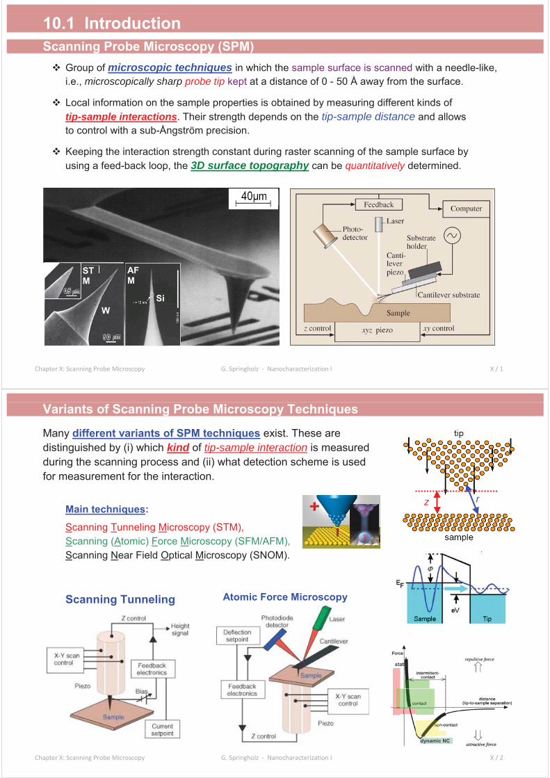
10.2.4 Nanomanipulation and Nanopatterning using SPMSPMs can be utilized not only for imaging but also for local manipulation and pattering of surfaces.Examples: Manipulation of single atoms (see below), nanolithography, nanopatterning as well as mechanical manipulation of nano-objects (see next page).
STM manipulation of iron atoms on a copper surface (Don Eigler et al., IBM)
Chapter X: Scanning Probe Microscopy G. Springholz - Nanocharacterization I X / 8
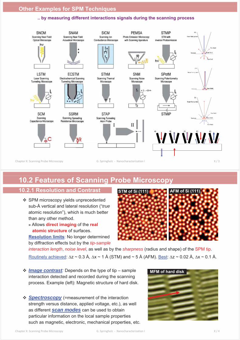
Manipulation of Nano-objects using SPM
Nano wire manipulation on polymer film using contact mode with a force of 2.2nN. Images taken in NC mode. Scan field 400 x 550 nm2.
Manipulation of 5 nm CdSe quantum dots on glass in air. Imaging with NC mode, Manipulation in contact mode. 1.0 x 0.6 μm2
Chapter X: Scanning Probe Microscopy G. Springholz - Nanocharacterization I X / 9
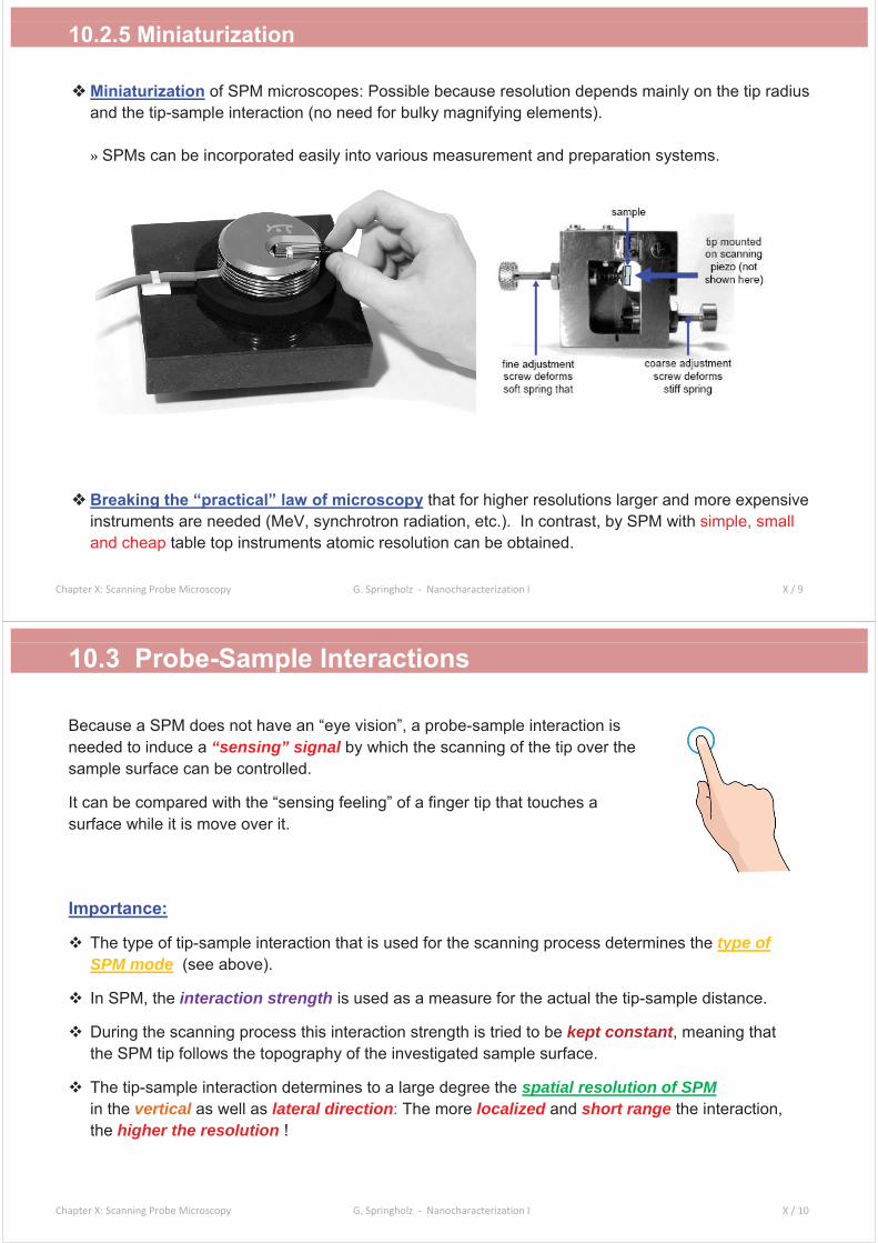
10.2.5 Miniaturization
Miniaturization of SPM microscopes: Possible because resolution depends mainly on the tip radius and the tip-sample interaction (no need for bulky magnifying elements).
» SPMs can be incorporated easily into various measurement and preparation systems.
Breaking the “practical” law of microscopy that for higher resolutions larger and more expensive instruments are needed (MeV, synchrotron radiation, etc.). In contrast, by SPM with simple, small and cheap table top instruments atomic resolution can be obtained.
Chapter X: Scanning Probe Microscopy G. Springholz - Nanocharacterization I X / 10
10.3 Probe-Sample Interactions
Because a SPM does not have an “eye vision”, a probe-sample interaction is needed to induce a “sensing” signal by which the scanning of the tip over the sample surface can be controlled.
It can be compared with the “sensing feeling” of a finger tip that touches a surface while it is move over it.
Importance:
The type of tip-sample interaction that is used for the scanning process determines the type of SPM mode (see above).
In SPM, the interaction strength is used as a measure for the actual the tip-sample distance.
During the scanning process this interaction strength is tried to be kept constant, meaning that the SPM tip follows the topography of the investigated sample surface.
The tip-sample interaction determines to a large degree the spatial resolution of SPMin the vertical as well as lateral direction: The more localized and short range the interaction, the higher the resolution !
Chapter X: Scanning Probe Microscopy G. Springholz - Nanocharacterization I X / 11
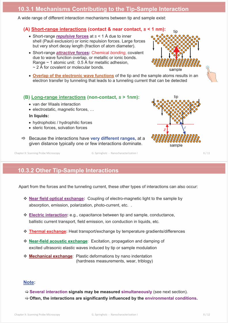
10.3.1 Mechanisms Contributing to the Tip-Sample InteractionA wide range of different interaction mechanisms between tip and sample exist:
(A) Short-range interactions (contact & near contact, s < 1 nm):Short-range repulsive forces at s < 1 Å due to inner shell (Pauli exclusion) or ionic repulsion forces. Large forces but very short decay length (fraction of atom diameter).Short-range attractive forces: Chemical bonding, covalent due to wave function overlap, or metallic or ionic bonds.Range ~ 1 atomic unit: 0.5 Å for metallic adhesion, ~ 2 Å for covalent or molecular bonds.
Overlap of the electronic wave functions of the tip and the sample atoms results in an electron transfer by tunneling that leads to a tunneling current that can be detected
(B) Long-range interactions (non-contact, s > 1nm):van der Waals interactionelectrostatic, magnetic forces, …
In liquids:hydrophobic / hydrophilic forcessteric forces, solvation forces
Because the interactions have very different ranges, at a given distance typically one or few interactions dominate.
rz
Chapter X: Scanning Probe Microscopy G. Springholz - Nanocharacterization I X / 12
10.3.2 Other Tip-Sample Interactions
Apart from the forces and the tunneling current, these other types of interactions can also occur:
Near field optical exchange: Coupling of electro-magnetic light to the sample by absorption, emission, polarization, photo-current, etc. .
Electric interaction: e.g., capacitance between tip and sample, conductance, ballistic current transport, field emission, ion conduction in liquids, etc.
Thermal exchange: Heat transport/exchange by temperature gradients/differences
Near-field acoustic exchange: Excitation, propagation and damping of excited ultrasonic elastic waves induced by tip or sample modulation
Several interaction signals may be measured simultaneously (see next section).Often, the interactions are significantly influenced by the environmental conditions.
Chapter X: Scanning Probe Microscopy G. Springholz - Nanocharacterization I X / 13
Application for various SPM Techniques
Measurement of additional interactions signals during the scanning process
Chapter X: Scanning Probe Microscopy G. Springholz - Nanocharacterization I X / 14
10.4 The Tunnelling Current: STMThe tunneling current flowing between tip and sample is the most simplest way to measure the tip-sample interaction and it is a good measure of the actual tip-sample distance.
Due to the tunneling effect, this current flows when there is an overlap of the wave functions even if there is no real physical contact between tip and sample. As a result, a current flows when a voltage is applied and the tip-sample distance if very small (~Å).
Outside of a solid, the electron wave functions decay exponentially with increasing distance from the surface, i.e., the probability of finding an electron outside of the solid of ~Å per decade.If two surfaces are brought very close to each other, the electron wave functions overlap and thus, acertain probability for tunneling of electrons through the vacuum from one solid to the other exists.
Chapter X: Scanning Probe Microscopy G. Springholz - Nanocharacterization I X / 15
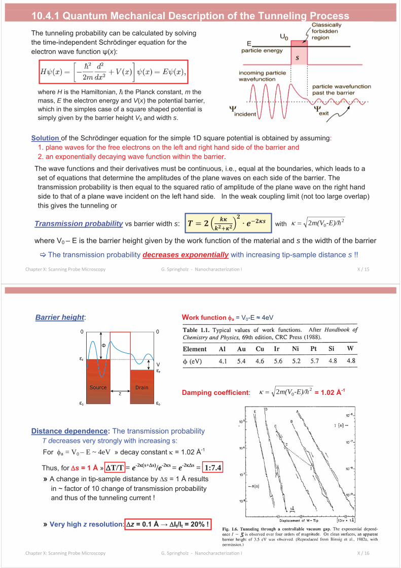
10.4.1 Quantum Mechanical Description of the Tunneling ProcessThe tunneling probability can be calculated by solving the time-independent Schrödinger equation for the electron wave function x):
where H is the Hamiltonian, the Planck constant, m the mass, E the electron energy and V(x) the potential barrier, which in the simples case of a square shaped potential is simply given by the barrier height V0 and width s.
Solution of the Schrödinger equation for the simple 1D square potential is obtained by assuming:1. plane waves for the free electrons on the left and right hand side of the barrier and 2. an exponentially decaying wave function within the barrier.
The wave functions and their derivatives must be continuous, i.e., equal at the boundaries, which leads to a set of equations that determine the amplitudes of the plane waves on each side of the barrier. The transmission probability is then equal to the squared ratio of amplitude of the plane wave on the right hand side to that of a plane wave incident on the left hand side. In the weak coupling limit (not too large overlap) this gives the tunneling or
Transmission probability vs barrier width s: = with 202 -E)/m(V
where V0 – E is the barrier height given by the work function of the material and s the width of the barrier
The transmission probability decreases exponentially with increasing tip-sample distance s !!
of the Tunneling Process
s
Chapter X: Scanning Probe Microscopy G. Springholz - Nanocharacterization I X / 16
Barrier height: Work function a = V0-
Damping coefficient: 202 -E)/m(V = 1.02 Å-1
Distance dependence: The transmission probability T decreases very strongly with increasing s:
For a = V0 – E ~ 4eV » decay constant = 1.02 Å-1
Thus, for s = 1 Å » T/T = e-2 s+ s)/e-2 s = e-2 s = 1:7.4» A change in tip-sample distance by s = 1 Å results
in ~ factor of 10 change of transmission probability and thus of the tunneling current !
» Very high z resolution: z It/It = 20% !
Chapter X: Scanning Probe Microscopy G. Springholz - Nanocharacterization I X / 17
10.4.2 Consequences for the Lateral Resolution of STM
The very high z resolution of STM [ It/It = 20% for z = 0.1 Å] results also in a very high lateral resolution x
due to the concentration of tunneling current at the apex of the STM tip where the distance s is minimal.
Simple estimate for the lateral resolution of STM:Lateral current distribution I(x) ~ T(x) for a spherical tip with radius R: (T = C .e- s)
s(x) = s0 + R (1-cos s0 + x2/2R and I(x) = I0. exp(-2 x2 / 2R)
Distance at which I(x) has decreased to 1/10 of I0:0.1. I0 = I0
. exp(-2 x2/2R) » x1/10 = (R.ln0.1/ )1/2
Example: R = 1000Å : x1/10
R = 100Å : x1/10
R = 10Å : x1/10
R = 2 Å : x1/10 2 Å
» Thus, a single atom at the end of the STM tip carries ~90% of tunneling current !
Å I(x)s(x)
x0
I(x)
Chapter X: Scanning Probe Microscopy G. Springholz - Nanocharacterization I X / 18
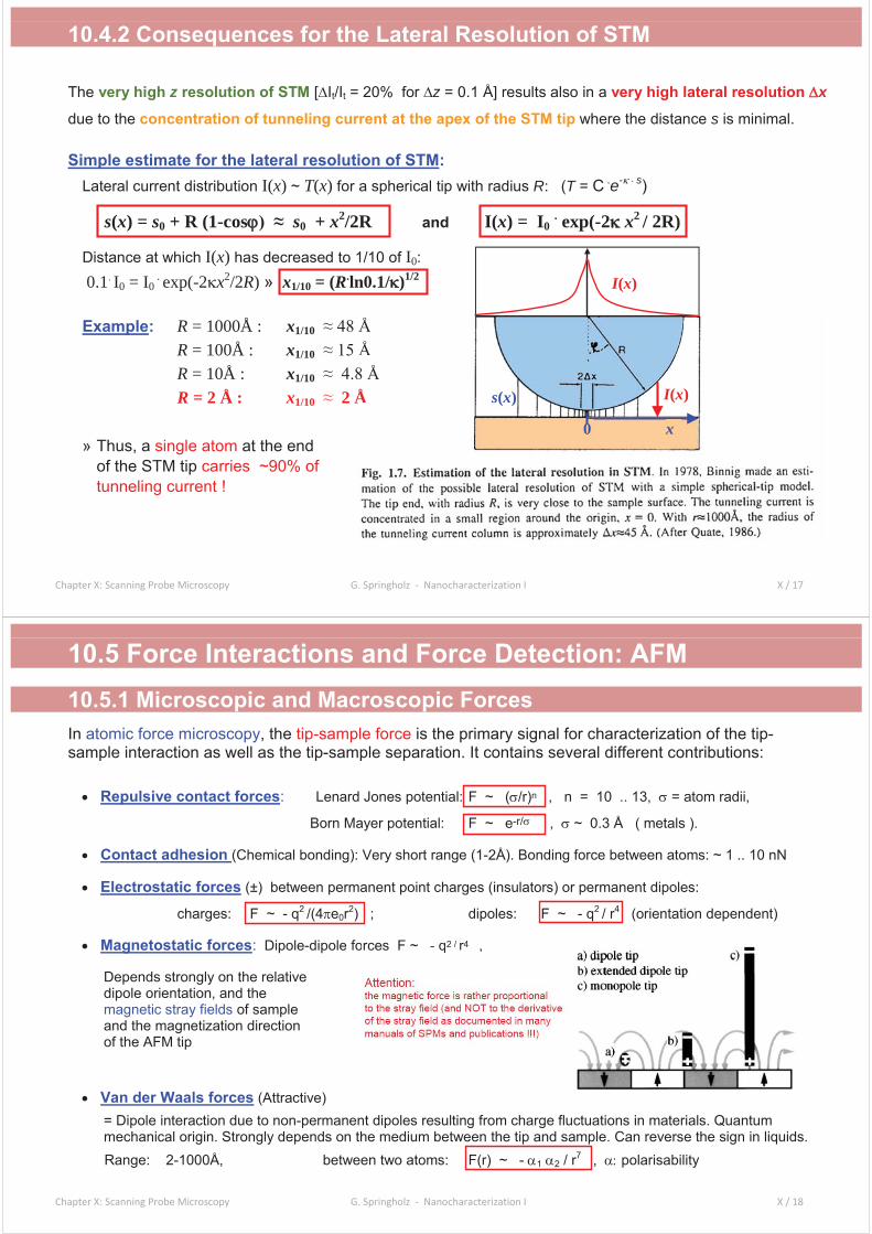
10.5 Force Interactions and Force Detection: AFM10.5.1 Microscopic and Macroscopic ForcesIn atomic force microscopy, the tip-sample force is the primary signal for characterization of the tip-sample interaction as well as the tip-sample separation. It contains several different contributions:
Repulsive contact forces: Lenard Jones potential: F ~ ( /r)n , n = 10 .. 13, = atom radii,
Born Mayer potential: F ~ e-r/ , ~ 0.3 Å ( metals ).
Contact adhesion (Chemical bonding): Very short range (1-2Å). Bonding force between atoms: ~ 1 .. 10 nN
Electrostatic forces (±) between permanent point charges (insulators) or permanent dipoles:
charges: F ~ - q2 /(4 e0r2) ; dipoles: F ~ - q2 / r4 (orientation dependent)
Depends strongly on the relative dipole orientation, and themagnetic stray fields of sample and the magnetization direction of the AFM tip
Van der Waals forces (Attractive)= Dipole interaction due to non-permanent dipoles resulting from charge fluctuations in materials. Quantum mechanical origin. Strongly depends on the medium between the tip and sample. Can reverse the sign in liquids. Range: 2-1000Å, between two atoms: F(r) ~ - 1 2 / r7 , polarisability
rces F ~ - q2 / r4rr ,
Chapter X: Scanning Probe Microscopy G. Springholz - Nanocharacterization I X / 19
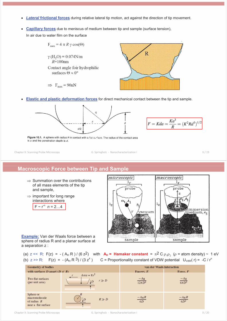
Lateral frictional forces during relative lateral tip motion, act against the direction of tip movement.
Capillary forces due to meniscus of medium between tip and sample (surface tension),
In air due to water film on the surface
Elastic and plastic deformation forces for direct mechanical contact between the tip and sample.
Chapter X: Scanning Probe Microscopy G. Springholz - Nanocharacterization I X / 20
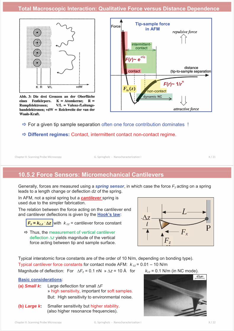
Macroscopic Force between Tip and Sample
Summation over the contributions of all mass elements of the tip and sample, important for long range interactions where F ~ r-n n = 2…4
Example: Van der Waals force between a sphere of radius R and a planar surface at a separation z :
(a) z << R: F(z) = - ( AH R ) / (6 z2) with AH = Hamaker constant = 2 C 1 ( = atom density) ~ 1 eV(b) z >> R: F(z) = - (AH R 3) / (3 z4 ) C = Proportionality constant of VDW potential UVdW( r) = -C / rn
Chapter X: Scanning Probe Microscopy G. Springholz - Nanocharacterization I X / 21
Total Macroscopic Interaction: Qualitative Force versus Distance Dependence
For a given tip sample separation often one force contribution dominates !
Different regimes: Contact, intermittent contact non-contact regime.
dynamic NC
)(zFts
Tip-sample force in AFM
F(r)~ e-r/
F(r)~ 1/rn
Chapter X: Scanning Probe Microscopy G. Springholz - Nanocharacterization I X / 22
10.5.2 Force Sensors: Micromechanical Cantilevers
Generally, forces are measured using a spring sensor, in which case the force Fz acting on a spring leads to a length change or deflection dz of the spring.In AFM, not a spiral spring but a cantilever spring is used due to the simpler fabrication.The relation between the force acting on the cantilever end and cantilever deflections is given by the Hook’s law:
Fz = kc,z. z with k cz = cantilever force constant
Thus, the measurement of vertical cantilever deflection z yields magnitude of the vertical force acting between tip and sample surface.
Typical interatomic force constants are of the order of 10 N/m, depending on bonding type).Typical cantilever force constants for contact mode AFM: k cz = 0.01 – 10 N/mMagnitude of deflection: For Fz = 0.1 nN » z = 10 Å for kcz = 0.1 N/m (in NC mode).
Basic considerations:(a) Small k: Large deflection for small F
» high sensitivity, important for soft samples.But: High sensitivity to environmental noise.
(b) Large k: Smaller sensitivity but higher stability.(also higher resonance frequencies).
z
Fz
Fx
Chapter X: Scanning Probe Microscopy G. Springholz - Nanocharacterization I X / 23
10.5.3 Cantilever Design
1. Spring constant in the range of 0.01 – 100 N/m:The force constant kcz of a cantilever is determined by its geometry, i.e., length L, thickness d andwidth w, as well as by the elastic constants (elastic modulus E ) of the cantilever material. For simple cantilever geometries with constant cantilever cross section, the force constant can be calculated analytically using elasticity theory
.Rectangular beam of width w, length L,and thickness d, elasticity module E andand a tip at a distance s from the end:
By choice of the geometry the spring constant can be tuned arbitrarily over a wide range !
Common cantilever and tip materials:
3
3
)(4 sLdwEkcz
w d
Chapter X: Scanning Probe Microscopy G. Springholz - Nanocharacterization I X / 24
Force Constant of Cantilevers with Different Cross-Sections
The influence of the cantilever shape is described by the moment of inertia dzzzwI 2)(where w(z) is the cross-sectional width of the cantilever at a distance z from the plane.
Verical Force Constanz kc,z:Rectangular beam:(width w and thickness d ):
Cantilever with the tip at a distance s from the end:
Circular rod:(length l, diameter d):
V-shaped cantilever:
Lateral Force Constant klateral
(Rectangular beam, tip height h): ( G = shear modulus)
wd
L
h
(length L, thickness d ,leg width w, half angle ,leg distance at base b)
wd L
2
3
2/dhLdwGklateral
1
3
3
3
32cos341cos
2 bw
LdwEkcz
33 LEIkcz
12
3dwIbar
4
4rIcylinder
3
3
4 LdwEkcz
3
3
43
LdEkcz
3
3
)(4 sLdwEkcz
Chapter X: Scanning Probe Microscopy G. Springholz - Nanocharacterization I X / 25
2. Dynamic response of the cantileverDuring the scanning process, the cantilever and tip should be able to follow the rapidly changing surface topography of the sample (=fast dynamical response) and the transient acceleration forces acting on the tip should be kept as small as possible:
The inertial cantilever mass size should be very small !This means small cantilever size, i.e., cantilever miniaturization.
3. Suppression of cantilever excitation
The cantilever should be immune against internal excitations arising from the scanning process as well as against external excitationsdue to mechanical vibrations, acoustic & thermal noise, .. ).
Example:2 μm scan of a 10 nm periodic structure with 5 Hz scan rate = 1 kHz vertical excitation of the cantilever30 nm scan of a 3 A atomic lattice with 10 Hz scan rate = 1 kHz vertical excitation of the cantileverAlternative: Low scan rates such as 1 Hz/line, 500 lines / image = 8 min / image
Generally, the reaction of a cantilever is similar to that of a damped harmonic oscillator.This means that the cantilever reacts strongly mainly to excitations with a frequency close to the Eigen-resonance frequency of the cantilever, i.e., the cantilever response speed is limited by the lowest cantilever resonance frequency due to simple bending oscillation.
» This resonance frequency o,res should be at above 10 kHz to prevent strong cantilever excitations !
F
Chapter X: Scanning Probe Microscopy G. Springholz - Nanocharacterization I X / 26
4. Resonance Frequency res of the Cantilever
The fundamental resonance frequency a simple spring-type harmonic oscillator (mass load attached to a spring) is given by:
For a cantilever sthe situation is somewhat different because the cantilever mass is distributed along the cantilever beam.Thus, different cantilever parts oscillate with different amplitude and velocity.
Rayleigh solution: = Equating the maximum kinetic energy and maximum strain energy of the cantilever, where: )sin(/)64(),( 422234
0 tLLxLxxztxz for the free ended cantilever.
By integration from x = 0 to L , one obtains: 20)6.1(2/1 zkE cstrain and
20
2)256.0(2/1 zmE ckin
Lowest frequency mode: or with additional(vertical bending mode) tip mass mtip:
Higher order modes:
with n = 1.875, 4.694, 7.855, 10.996, …. . and
LAVmc and 333 4//3 LdwELEIk
V-shaped cantilever:
AIE
Ln
n 2
2
c
cres m
k24.0 tipc
cres mm
k24.0
mkres /
tipc
cres mm
k163.0
Chapter X: Scanning Probe Microscopy G. Springholz - Nanocharacterization I X / 27
From the equations above it follows that for a given k-value, defined by the geometry and shape of the beam, a high resonance frequency can be achieved by reducing the cantilever mass.
This means miniaturization of the cantilever beams to achieve a high resonance frequency !
If w and the d/L ratio is fixed, then k is constant and res increases if L is made very small.
Example: Rectangular bar-shaped cantilevers made of silicon
SEM images of 3 rectangular silicon cantilevers (A, B, C) with two different length series.
Specifications for different cantilever parameters
Chapter X: Scanning Probe Microscopy G. Springholz - Nanocharacterization I X / 28
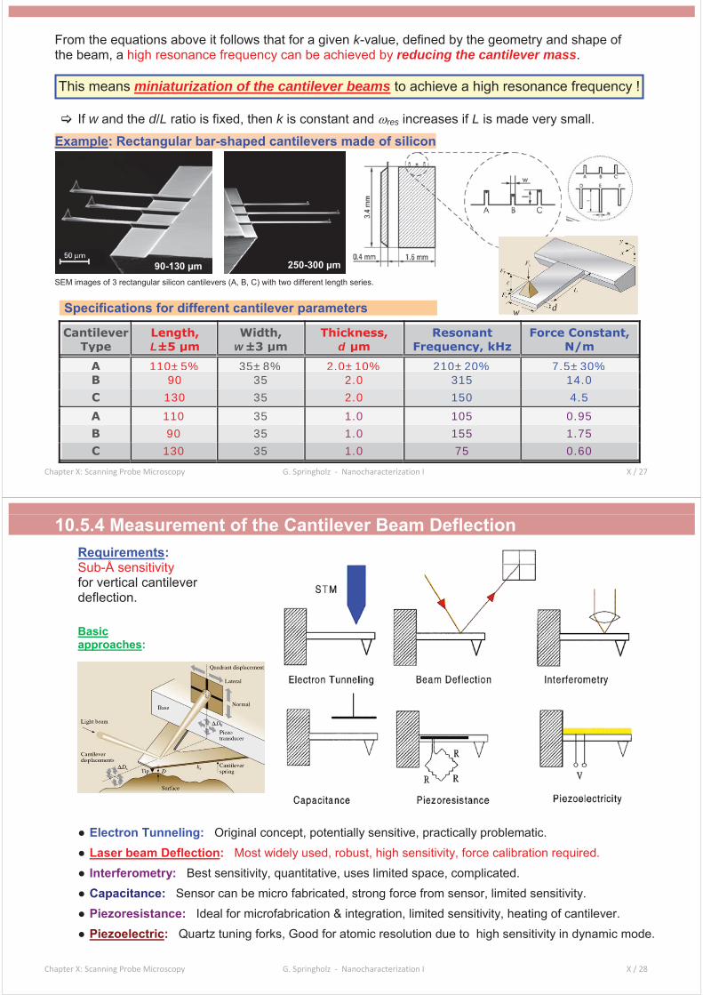
10.5.4 Measurement of the Cantilever Beam DeflectionRequirements:Sub-Å sensitivityfor vertical cantilever deflection.
Basic approaches:
Electron Tunneling: Original concept, potentially sensitive, practically problematic.Laser beam Deflection: Most widely used, robust, high sensitivity, force calibration required.Interferometry: Best sensitivity, quantitative, uses limited space, complicated.Capacitance: Sensor can be micro fabricated, strong force from sensor, limited sensitivity.Piezoresistance: Ideal for microfabrication & integration, limited sensitivity, heating of cantilever.Piezoelectric: Quartz tuning forks, Good for atomic resolution due to high sensitivity in dynamic mode.
Chapter X: Scanning Probe Microscopy G. Springholz - Nanocharacterization I X / 29
Optical Beam Deflection Measurement Systems
Chapter X: Scanning Probe Microscopy G. Springholz - Nanocharacterization I X / 30
10.6 Comparison: Atomic Resolution in AFM / STMAtomic resolution in AFM is much more difficult to achieve than in STM because the local interaction force between the final atom at the end of the tip and the surface atoms of the sample is superimposed by the large contribution of long-range van der Waals and other forces.
Therefore, in AFM atomic resolution can be achieved only by scanning the tip very close to the surface such that the tip force is able to sense the temporary local bonding due to overlap of the atomic orbitals of the tip and sample atoms and by using very high sensitivity AC modulation force measure-ment schemes (see Sect. 10.10 below).
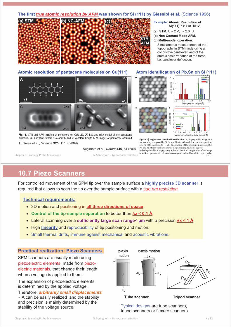
Sugimoto et al., Nature 446, 64 (2007).
Chapter X: Scanning Probe Microscopy G. Springholz - Nanocharacterization I X / 31
The first true atomic resolution by AFM was shown for Si (111) by Giessibl et al. (Science 1996)
Atomic resolution of pentacene molecules on Cu(111) Atom identification of Pb,Sn on Si (111)
Example: Atomic Resolution of Si(111) 7 x 7 in UHV(a) STM: U = 2 V, I = 2.0 nA, (b) Non-Contact Mode AFM, (c) Multi-mode operation:
Simultaneous measurement of the topography in STM mode using a conductive cantilever, and of the atomic scale variation of the force, i.e. cantilever deflection.
(a) STM (b) NC-AFM (c)
AFMSTM
L. Gross et al., Science 325, 1110 (2009).
Sugimoto et al., Nature 446, 64 (2007).
n I X ///// 331333333
).
Chapter X: Scanning Probe Microscopy G. Springholz - Nanocharacterization I X / 32
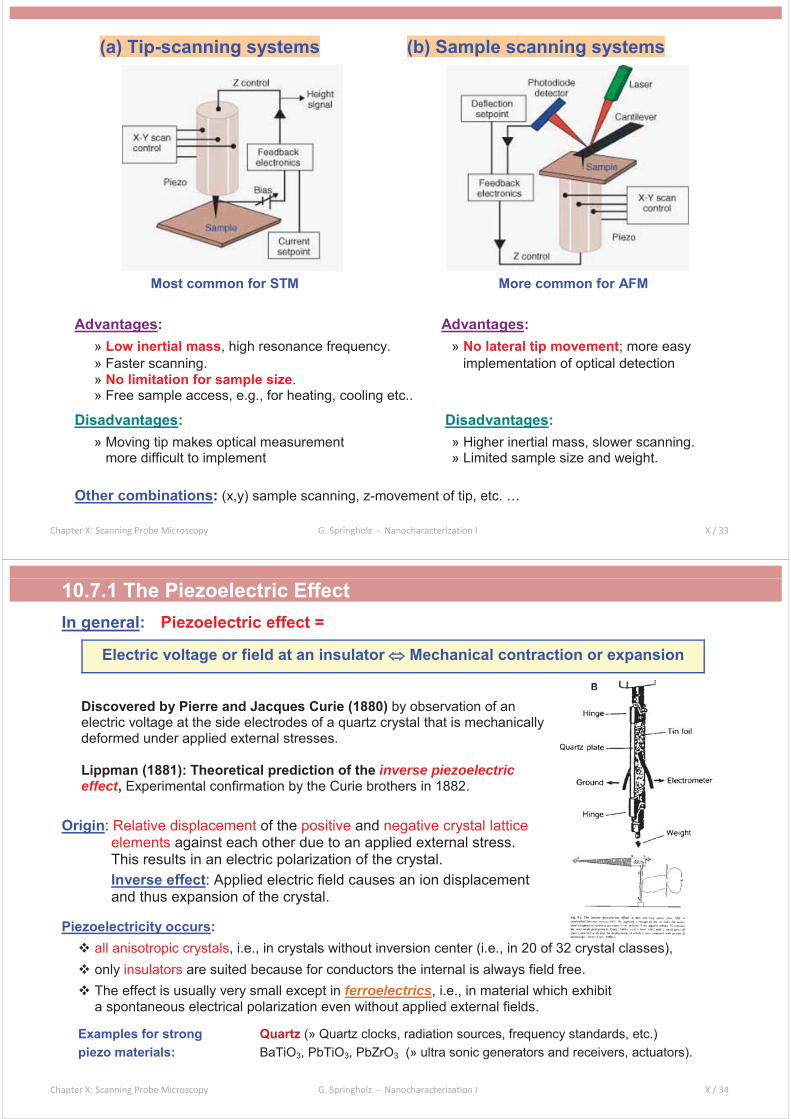
10.7 Piezo ScannersFor controlled movement of the SPM tip over the sample surface a highly precise 3D scanner is required that allows to scan the tip over the sample surface with a sub-nm resolution.
Technical requirements: 3D motion and positioning in all three directions of spaceControl of the tip-sample separation to better than z < 0.1 Å,Lateral scanning over a sufficiently large scan range< μm with a precision x < 1 Å,High linearity and reproducibility of tip positioning and motion,Small thermal drifts, immune against mechanical and acoustic vibrations.
Practical realization: Piezo ScannersSPM scanners are usually made using piezoelectric elements, made from piezo-electric materials, that change their length when a voltage is applied to them.The expansion of piezoelectric elements is determined by the applied voltage. Therefore, arbitrarily small displacements~ Å can be easily realized and the stability and precision is mainly determined by the stability of the voltage source.
Tripod scannerTube scanner
Typical designs are tube scanners, tripod scanners or flexure scanners.
Chapter X: Scanning Probe Microscopy G. Springholz - Nanocharacterization I X / 33
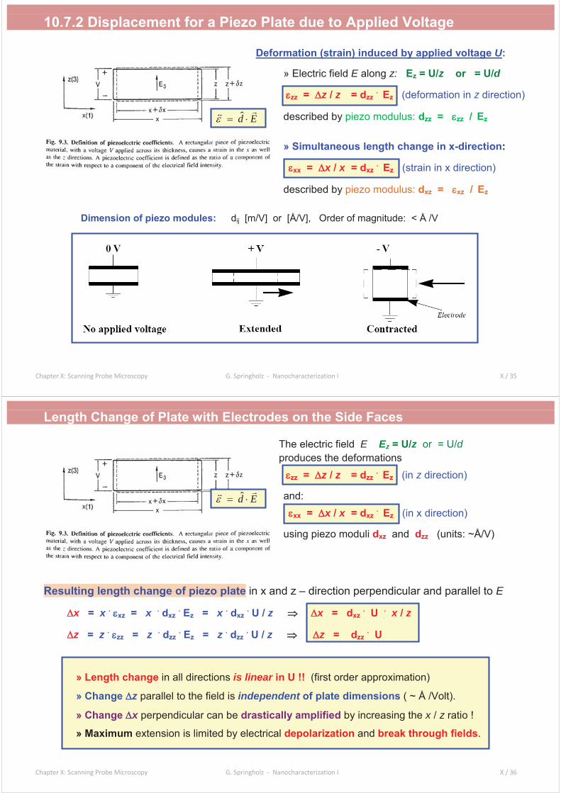
(a) Tip-scanning systems (b) Sample scanning systems
Most common for STM More common for AFM
Advantages: Advantages:» Low inertial mass, high resonance frequency. » No lateral tip movement; more easy» Faster scanning. implementation of optical detection» No limitation for sample size.» Free sample access, e.g., for heating, cooling etc..
Disadvantages: Disadvantages:» Moving tip makes optical measurement » Higher inertial mass, slower scanning.
more difficult to implement » Limited sample size and weight.
Other combinations: (x,y) sample scanning, z-movement of tip, etc. …
Chapter X: Scanning Probe Microscopy G. Springholz - Nanocharacterization I X / 34
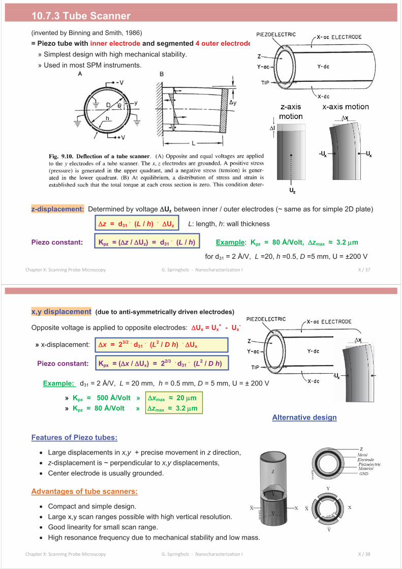
10.7.1 The Piezoelectric EffectIn general: Piezoelectric effect =
Electric voltage or field at an insulator Mechanical contraction or expansion
Discovered by Pierre and Jacques Curie (1880) by observation of an electric voltage at the side electrodes of a quartz crystal that is mechanically deformed under applied external stresses.
Lippman (1881): Theoretical prediction of the inverse piezoelectric effect, Experimental confirmation by the Curie brothers in 1882.
Origin: Relative displacement of the positive and negative crystal latticeelements against each other due to an applied external stress. This results in an electric polarization of the crystal. Inverse effect: Applied electric field causes an ion displacement and thus expansion of the crystal.
Piezoelectricity occurs:all anisotropic crystals, i.e., in crystals without inversion center (i.e., in 20 of 32 crystal classes),only insulators are suited because for conductors the internal is always field free.The effect is usually very small except in ferroelectrics, i.e., in material which exhibit a spontaneous electrical polarization even without applied external fields.
Examples for strong Quartz (» Quartz clocks, radiation sources, frequency standards, etc.)piezo materials: BaTiO3, PbTiO3, PbZrO3 (» ultra sonic generators and receivers, actuators).
Chapter X: Scanning Probe Microscopy G. Springholz - Nanocharacterization I X / 35
10.7.2 Displacement for a Piezo Plate due to Applied Voltage
Deformation (strain) induced by applied voltage U:
» Electric field E along z: Ez = U/z or = U/d
zz = z / z = dzz. Ez (deformation in z direction)
described by piezo modulus: dzz = zz / Ez
» Simultaneous length change in x-direction:
xx = x / x = dxz. Ez (strain in x direction)
described by piezo modulus: dxz = xz / Ez
Dimension of piezo modules: dij [m/V] or [Å/V], Order of magnitude: < Å /V
ˆ Ed
Chapter X: Scanning Probe Microscopy G. Springholz - Nanocharacterization I X / 36
Length Change of Plate with Electrodes on the Side Faces
The electric field E Ez = U/z or = U/dproduces the deformations
zz = z / z = dzz. Ez (in z direction)
and:
xx = x / x = dxz. Ez (in x direction)
using piezo moduli dxz and dzz (units: ~Å/V)
Resulting length change of piezo plate in x and z – direction perpendicular and parallel to E
x = x .xz = x . dxz
. Ez = x . dxz. U / z x = dxz
. U . x / z
z = z .zz = z . dzz
. Ez = z . dzz. U / z z = dzz
. U
» Length change in all directions is linear in U !! (first order approximation)
» Change z parallel to the field is independent of plate dimensions ( ~ Å /Volt).
» Change x perpendicular can be drastically amplified by increasing the x / z ratio !
» Maximum extension is limited by electrical depolarization and break through fields.
ˆ Ed
Chapter X: Scanning Probe Microscopy G. Springholz - Nanocharacterization I X / 37
10.7.3 Tube Scanner(invented by Binning and Smith, 1986)= Piezo tube with inner electrode and segmented 4 outer electrodes.
» Simplest design with high mechanical stability. » Used in most SPM instruments.
z-displacement: Determined by voltage Uz between inner / outer electrodes (~ same as for simple 2D plate)
z = d31. (L / h) . Uz L: length, h: wall thickness
Piezo constant: Kpz = ( z / Uz) = d31. (L / h) Example: Kpz = 80 Å/Volt, zmax m
for d31 = 2 Å/V, L =20, h =0.5, D =5 mm, U = ±200 V
Chapter X: Scanning Probe Microscopy G. Springholz - Nanocharacterization I X / 38
x,y displacement (due to anti-symmetrically driven electrodes)
Opposite voltage is applied to opposite electrodes: Ux = Ux+ - Ux
-
» x-displacement: x = 23/2 . d31. (L2 / D h) . Ux
Piezo constant: Kpx = ( x / Ux) = 22/3 . d31. (L2 / D h)
Example: d31 = 2 Å/V, L = 20 mm, h = 0.5 mm, D = 5 mm, U = ± 200 V
Large displacements in x,y + precise movement in z direction, z-displacement is ~ perpendicular to x,y displacements,Center electrode is usually grounded.
Advantages of tube scanners:
Compact and simple design.Large x,y scan ranges possible with high vertical resolution.Good linearity for small scan range.High resonance frequency due to mechanical stability and low mass.
Alternative design
Chapter X: Scanning Probe Microscopy G. Springholz - Nanocharacterization I X / 39
10.7.4 Flexure Scanner (x,y)= Combination of piezo stacks and flexible arms
Advantages:
Decoupling of x-y and of z motions,Planar 2D scanning in the x-y direction,Decoupled extra piezo tube for z-movement.
z = N . dzz. U = N . 3-5 Å/V . U
Chapter X: Scanning Probe Microscopy G. Springholz - Nanocharacterization I X / 40
10.8 Imaging Strategies and Scan ModesThe imaging or scanning process of an SPM can be compared to a blind exploration of an object or environment by a probe stick (similar as a blind person with his stick) without having any vision or pre-knowledge on the topography of the sample.
Scan strategies: To solve this problem, one has to devise an efficient way onhow to scan the objects without any prior knowledge about their structure and morphology. The goal is to explore the topography without damaging the probe tipor the sample, i.e., by avoiding too strong contact that would destroy the tip.
The only feedback sensing signal available this exploration process is the measurement of the strength of the tip-sample interaction. Due to the strong non-linearity of the tip-sample interaction,it is, however, only an indirect measure of the actual tip-sample distance.
Two fundamental scan and imaging approaches can be used, called constant height or constant interaction scan mode.
In addition, further scan modes exists such a hybrid or multi-pass scan modes in which usually different types of interaction signals are recorded simultaneously or sequentially, which allows to obtain additional, non-topographic information such as electrical, magnetic or other properties.
Chapter X: Scanning Probe Microscopy G. Springholz - Nanocharacterization I X / 41
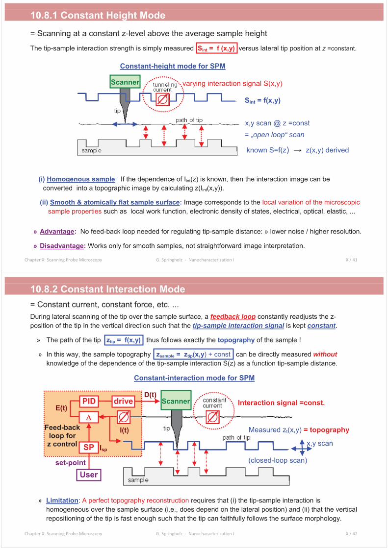
10.8.1 Constant Height Mode
= Scanning at a constant z-level above the average sample height
The tip-sample interaction strength is simply measured Sint = f (x,y) versus lateral tip position at z =constant.
(i) Homogenous sample: If the dependence of Iint(z) is known, then the interaction image can be converted into a topographic image by calculating z(Iint(x,y)).
(ii) Smooth & atomically flat sample surface: Image corresponds to the local variation of the microscopic sample properties such as local work function, electronic density of states, electrical, optical, elastic, ...
» Advantage: No feed-back loop needed for regulating tip-sample distance: » lower noise / higher resolution.
» Disadvantage: Works only for smooth samples, not straightforward image interpretation.
x,y scan @ z =const= „open loop“ scan
varying interaction signal S(x,y)
Constant-height mode for SPM
Sint = f(x,y)
known S=f(z) z(x,y) derived
Scanner
Chapter X: Scanning Probe Microscopy G. Springholz - Nanocharacterization I X / 42
10.8.2 Constant Interaction Mode = Constant current, constant force, etc. ...During lateral scanning of the tip over the sample surface, a feedback loop constantly readjusts the z-position of the tip in the vertical direction such that the tip-sample interaction signal is kept constant.
» The path of the tip ztip = f(x,y) thus follows exactly the topography of the sample !
» In this way, the sample topography zsample = ztip(x,y) + const can be directly measured withoutknowledge of the dependence of the tip-sample interaction S(z) as a function tip-sample distance.
» Limitation: A perfect topography reconstruction requires that (i) the tip-sample interaction is homogeneous over the sample surface (i.e., does depend on the lateral position) and (ii) that the vertical repositioning of the tip is fast enough such that the tip can faithfully follows the surface morphology.
x,y scan
(closed-loop scan)
Interaction signal =const.
Measured zt(x,y) = topographyFeed-back loop for z control
ScannerPID drive
SP
Userset-point
E(t)
I(t)
Isp
D(t)
Constant-interaction mode for SPM
Chapter X: Scanning Probe Microscopy G. Springholz - Nanocharacterization I X / 43
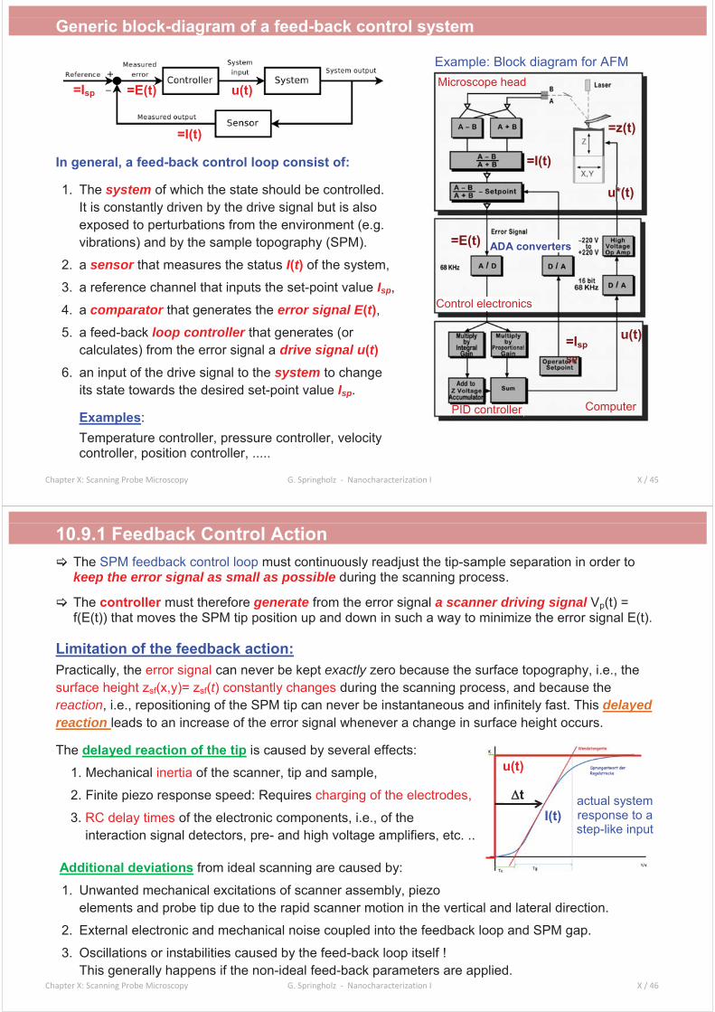
Comparison: Constant current vs. constant height mode
Example : STM imaging of highly ordered pyrolithic graphite
(a) Topography in constant current mode (b) Current image in constant height mode.
Generally: Samples are neither atomically flat nor physically homogenous:
Then, the SPM measurement corresponds to a superposition of topographic and interaction information. Separation possible only by application of spectroscopic techniques or multi-pass scan modes (see below).
Topography Current image
Chapter X: Scanning Probe Microscopy G. Springholz - Nanocharacterization I X / 44
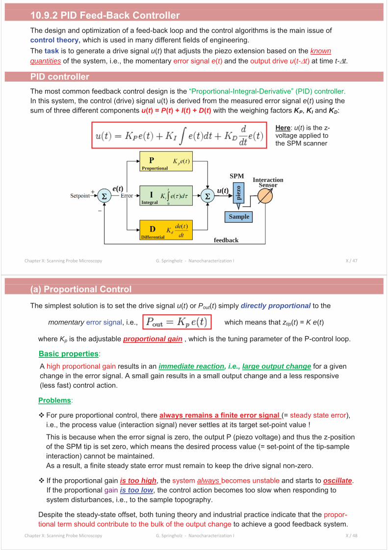
10.9 Feedback Loop and Scan ControlTo perform a constant interaction scan, an electronic feed-back control loop is needed to keep the tip-sample distance constant during the scanning process and to reconstruct the surface topography.
Working principle of the feed-back Loop:
(1)+(2): In the feed-back loop, the measured interaction signal I(t) (1) is constantly compared to the user chosen set-point interaction Isp value (2).
(3) The difference between signal and set-point yields the so-called error signal E(t) = I(t) - Isp (3)
Case #1: When the error signal is zero, the interaction strength is equal to the desired set point. Thus, the tip-sample distance has the correct value and the z- extension should be unchanged.
Case #2: If the error signal is non zero, a drive voltage u(t) = f(E(t)) (4) must be generated and applied to the scanner to change the z-position of the tip until the measured interaction signal again reaches the desired set point value, i.e., until the error signal again goes to zero.
If the error signal E(t) is always ~ zero during the scanning process, then the tip follows exactlythe surface topography zsf(x,y). The topography is then simply given by: zscanner(x,y)
Constant interaction signal
s = const.
Feed-back loop for z control
ScannerPID drive
SP
Userset-point
E(t)
I(t)
Isp
SP
u(t)
(1)
pp(2)
(3)(4)
Chapter X: Scanning Probe Microscopy G. Springholz - Nanocharacterization I X / 45
Generic block-diagram of a feed-back control system
In general, a feed-back control loop consist of:
1. The system of which the state should be controlled.It is constantly driven by the drive signal but is also exposed to perturbations from the environment (e.g. vibrations) and by the sample topography (SPM).
2. a sensor that measures the status I(t) of the system,3. a reference channel that inputs the set-point value Isp,
4. a comparator that generates the error signal E(t),5. a feed-back loop controller that generates (or
calculates) from the error signal a drive signal u(t)6. an input of the drive signal to the system to change
its state towards the desired set-point value Isp.
Examples:Temperature controller, pressure controller, velocity controller, position controller, .....
=I(t)
u(t)=E(t)=IspMicroscope head
=I(t)
=Isp
SP
u(t)
Example: Block diagram for AFM
Control electronics
u*(t)
=E(t)
=z(t)
ComputerPID controller
ADA converters
Chapter X: Scanning Probe Microscopy G. Springholz - Nanocharacterization I X / 46
10.9.1 Feedback Control Action The SPM feedback control loop must continuously readjust the tip-sample separation in order to keep the error signal as small as possible during the scanning process.
The controller must therefore generate from the error signal a scanner driving signal Vp(t) = f(E(t)) that moves the SPM tip position up and down in such a way to minimize the error signal E(t).
Limitation of the feedback action:Practically, the error signal can never be kept exactly zero because the surface topography, i.e., the surface height zsf(x,y)= zsf(t) constantly changes during the scanning process, and because thereaction, i.e., repositioning of the SPM tip can never be instantaneous and infinitely fast. This delayed reaction leads to an increase of the error signal whenever a change in surface height occurs.
The delayed reaction of the tip is caused by several effects: 1. Mechanical inertia of the scanner, tip and sample,2. Finite piezo response speed: Requires charging of the electrodes,
3. RC delay times of the electronic components, i.e., of the interaction signal detectors, pre- and high voltage amplifiers, etc. ..
Additional deviations from ideal scanning are caused by:
1. Unwanted mechanical excitations of scanner assembly, piezo elements and probe tip due to the rapid scanner motion in the vertical and lateral direction.
2. External electronic and mechanical noise coupled into the feedback loop and SPM gap.
3. Oscillations or instabilities caused by the feed-back loop itself !This generally happens if the non-ideal feed-back parameters are applied.
u(t)
I(t)actual system response to a step-like input
t
Chapter X: Scanning Probe Microscopy G. Springholz - Nanocharacterization I X / 47
10.9.2 PID Feed-Back ControllerThe design and optimization of a feed-back loop and the control algorithms is the main issue of control theory, which is used in many different fields of engineering. The task is to generate a drive signal u(t) that adjusts the piezo extension based on the known quantities of the system, i.e., the momentary error signal e(t) and the output drive u(t- t) at time t- t.
PID controllerThe most common feedback control design is the “Proportional-Integral-Derivative” (PID) controller.In this system, the control (drive) signal u(t) is derived from the measured error signal e(t) using the sum of three different components u(t) = P(t) + I(t) + D(t) with the weighing factors KP, KI and KD:
InteractionSensor
feedback
Proportional
Integral
Differential
SPM
piez
o
Sample
u(t)e(t)
Here: u(t) is the z-voltage applied to the SPM scanner
Chapter X: Scanning Probe Microscopy G. Springholz - Nanocharacterization I X / 48
(a) Proportional Control
The simplest solution is to set the drive signal u(t) or Pout(t) simply directly proportional to the
momentary error signal, i.e., which means that ztip(t) = K e(t)
where Kp is the adjustable proportional gain , which is the tuning parameter of the P-control loop.
Basic properties:A high proportional gain results in an immediate reaction, i.e., large output change for a given change in the error signal. A small gain results in a small output change and a less responsive (less fast) control action.
Problems:
For pure proportional control, there always remains a finite error signal (= steady state error), i.e., the process value (interaction signal) never settles at its target set-point value !
This is because when the error signal is zero, the output P (piezo voltage) and thus the z-position of the SPM tip is set zero, which means the desired process value (= set-point of the tip-sample interaction) cannot be maintained. As a result, a finite steady state error must remain to keep the drive signal non-zero.
If the proportional gain is too high, the system always becomes unstable and starts to oscillate.If the proportional gain is too low, the control action becomes too slow when responding to system disturbances, i.e., to the sample topography.
Despite the steady-state offset, both tuning theory and industrial practice indicate that the propor-tional term should contribute to the bulk of the output change to achieve a good feedback system.
Chapter X: Scanning Probe Microscopy G. Springholz - Nanocharacterization I X / 49
(b) Integral Control
The idea behind the integral control loop is to change the output I(t) , i.e., system reaction directly proportional to the momentary error signal e(t), i.e.:
In simple terms, this means that if the error signal is zero, the system keeps in its current state, and if not, its speed of reaction is directly proportional to the magnitude of the error signal, i.e., large error means fast reaction, small error means slow reaction. By integration over time, the actual output value Iout is derived as: ( ) = / = ( )
Thus, according to this algorithm the actual drive signal Iout(t) is proportional to the time integratederror signal. Ki is the adjustable integral gain and also the integration time can be varied.
Basic properties:1. The integral term adds to the momentary output a value proportional to the momentary error:
Thus: i.e.,The new output at time t is obtained by adding the just measured Kie(t) to the previous output at (t-dt).
2. The integral control term completely eliminates the residual steady state error !Reason: The output Iout is changed only if the error signal is non-zero. When the target value is reached the drive signal Iout is kept constant. Thus, the integral term always drives the process towards the correct set point.
3. Drawback: Because the integral term is proportional to the accumulated errors from the past, a quite large delay and overshoot over the set point value usually occurs and response is slow.
)(/)()(~)( teKdttdItetI ioutout
)()()(0
eKdeKtI idtt
iout )()()( eKdttItI ioutout
Chapter X: Scanning Probe Microscopy G. Springholz - Nanocharacterization I X / 50
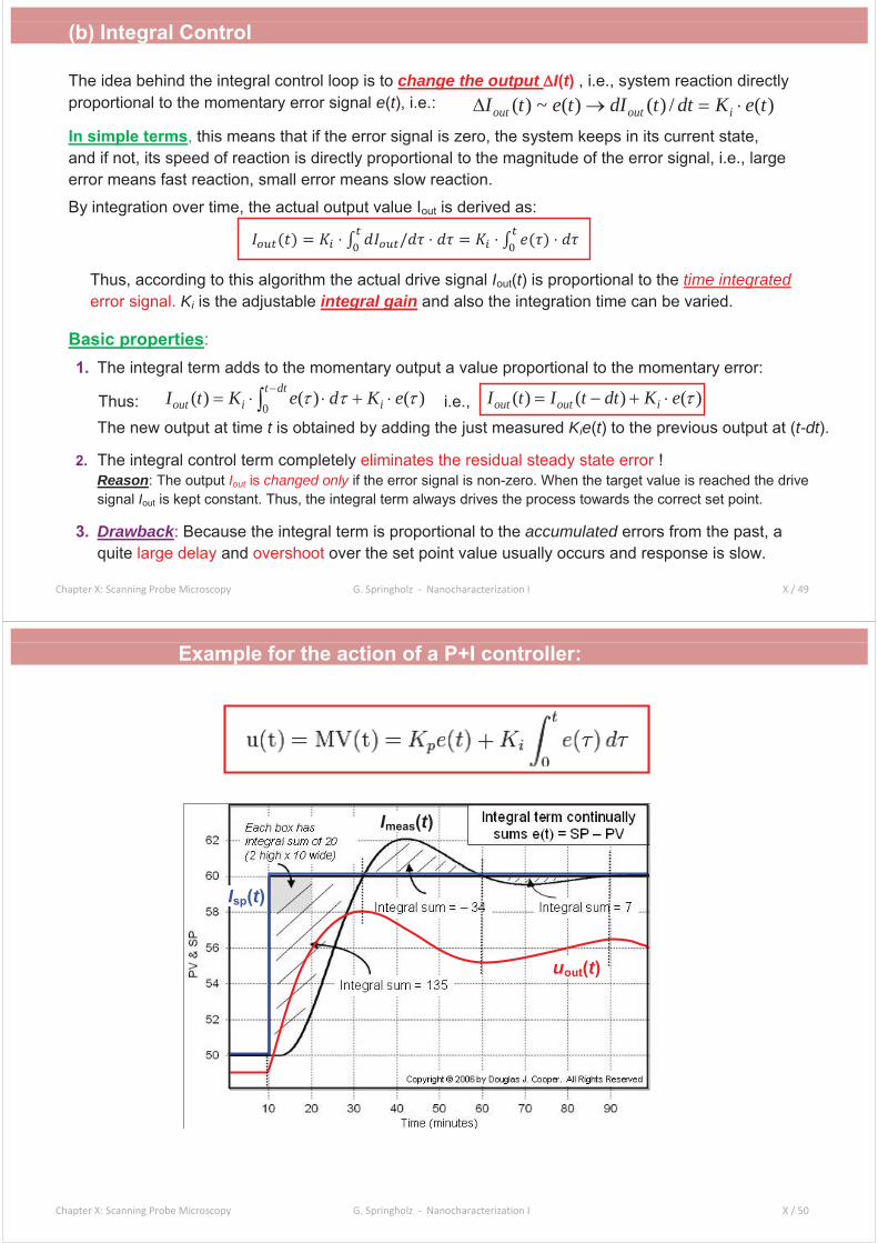
Example for the action of a P+I controller:
uout(t)
Imeas(t)
Isp(t)
Chapter X: Scanning Probe Microscopy G. Springholz - Nanocharacterization I X / 51
(c) Derivative Control
Idea: To reduce the overshoot, an additional term is added to the output u(t) = Dout(t) that is set
proportional to the time derivative (slope) of the error signal de/dt:
Thus, when the system approaches the set-point very fast, the drive signal is reduced already before the set-point is actually reached. The strength of this contribution is given by the derivative gain Kd.
Basic properties:1. The derivative control term can improve the dynamical behavior of the system, because the
time derivative takes into account the speed at which the set point of the system is approached.If the speed is very fast, then the derivative term can reduce the control output already before the actual set-point value is reached.Thus, the derivative term anticipates the response of the control system (=“look-ahead” gain)and reduces the overshoot of the system.
2. A derivative control term alone never leads to a stable control system.It can be used only in conjunction with a proportional or integral control term.
3. Although derivative control improves the response time of the system, it also makes it more unstable because even small perturbations and noise are strongly amplified in the feed back loop.As a result, in most cases the derivative gain is set to zero in most SPM applications.
Chapter X: Scanning Probe Microscopy G. Springholz - Nanocharacterization I X / 52
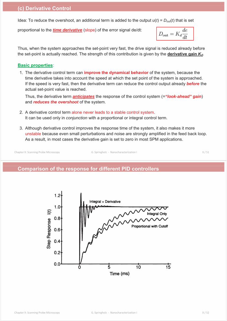
Comparison of the response for different PID controllers
Chapter X: Scanning Probe Microscopy G. Springholz - Nanocharacterization I X / 53
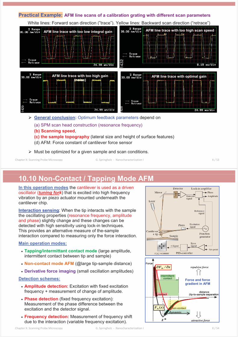
Practical Example: AFM line scans of a calibration grating with different scan parameters
White lines: Forward scan direction (”trace”). Yellow lines: Backward scan direction (“retrace”)
General conclusion: Optimum feedback parameters depend on(a) SPM scan head construction (resonance frequency)(b) Scanning speed,(c) the sample topography (lateral size and height of surface features)(d) AFM: Force constant of cantilever force sensor
Must be optimized for a given sample and scan conditions.
( )
AFM line trace with too low integral gain
AFM line trace with optimal gain
AFM line trace with too high scan speed
AFM line trace with too high gain (noise)
Chapter X: Scanning Probe Microscopy G. Springholz - Nanocharacterization I X / 54
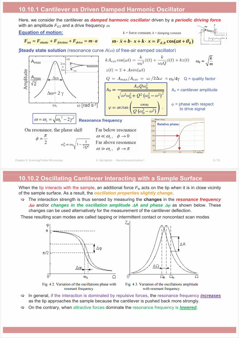
10.10 Non-Contact / Tapping Mode AFMIn this operation modes the cantilever is used as a driven oscillator (tuning fork) that is excited into high frequency vibration by an piezo actuator mounted underneath the cantilever chip.
Interaction sensing: When the tip interacts with the sample the oscillating properties (resonance frequency, amplitude and phase) slightly change and these changes can be detected with high sensitivity using lock-in techniques. This provides an alternative measure of the-sample interaction compared to measuring only the force interaction.
Main operation modes:Tapping/intermittant contact mode (large amplitude, intermittent contact between tip and sample)
Non-contact mode AFM (@large tip-sample distance)
Derivative force imaging (small oscillation amplitudes)
Detection schemes:Amplitude detection: Excitation with fixed excitation frequency + measurement of change of amplitude.
Phase detection (fixed frequency excitation): Measurement of the phase difference between the excitation and the detector signal.
Frequency detection: Measurement of frequency shiftdue to the interaction (variable frequency excitation).
dynamic
zFts /
)(zFts
Force and force gradient in AFM
*z
Chapter X: Scanning Probe Microscopy G. Springholz - Nanocharacterization I X / 55
10.10.1 Cantilever as Driven Damped Harmonic Oscillator Here, we consider the cantilever as damped harmonic oscillator driven by a periodic driving forcewith an amplitude Fd,0 and a drive frequency .Equation of motion:
Steady state solution (resonance curve A( ) of free-air eamped oscillator)( ( ) p )
Q = quality factor
A0 = cantilever amplitude
= phase with respect to drive signal
Resonance frequency
k = force constant, b = damping constant
amFFFF drivefrictionelastictot )cos( 00, tFxkxbxm d
Relative phase:
= r/4
= 2
Chapter X: Scanning Probe Microscopy G. Springholz - Nanocharacterization I X / 56
10.10.2 Oscillating Cantilever Interacting with a Sample SurfaceWhen the tip interacts with the sample, an additional force Fts acts on the tip when it is in close vicinity of the sample surface. As a result, the oscillation properties slightly change.
The interaction strength is thus sensed by measuring the changes in the resonance frequencyand/or changes in the oscillation amplitude A and phase as shown below. These
changes can be used alternatively for the measurement of the cantilever deflection. These resulting scan modes are called tapping or intermittent contact or noncontact scan modes
In general, if the interaction is dominated by repulsive forces, the resonance frequency increasesas the tip approaches the sample because the cantilever is pushed back more strongly. On the contrary, when attractive forces dominate the resonance frequency is lowered.
Chapter X: Scanning Probe Microscopy G. Springholz - Nanocharacterization I X / 57
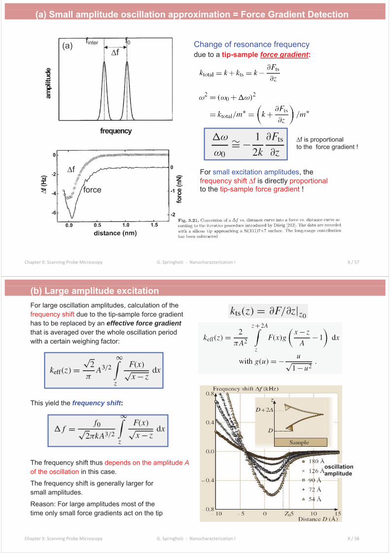
(a) Small amplitude oscillation approximation = Force Gradient Detection
Change of resonance frequency due to a tip-sample force gradient:
f0finter
force
f For small excitation amplitudes, the frequency shift f is directly proportional to the tip-sample force gradient !
f is proportional to the force gradient !
Chapter X: Scanning Probe Microscopy G. Springholz - Nanocharacterization I X / 58
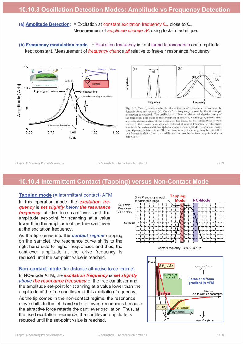
(b) Large amplitude excitation For large oscillation amplitudes, calculation of the frequency shift due to the tip-sample force gradient has to be replaced by an effective force gradientthat is averaged over the whole oscillation period with a certain weighing factor:
This yield the frequency shift:
The frequency shift thus depends on the amplitude Aof the oscillation in this case.
The frequency shift is generally larger for small amplitudes.
Reason: For large amplitudes most of the time only small force gradients act on the tip
oscillation amplitude
Chapter X: Scanning Probe Microscopy G. Springholz - Nanocharacterization I X / 59
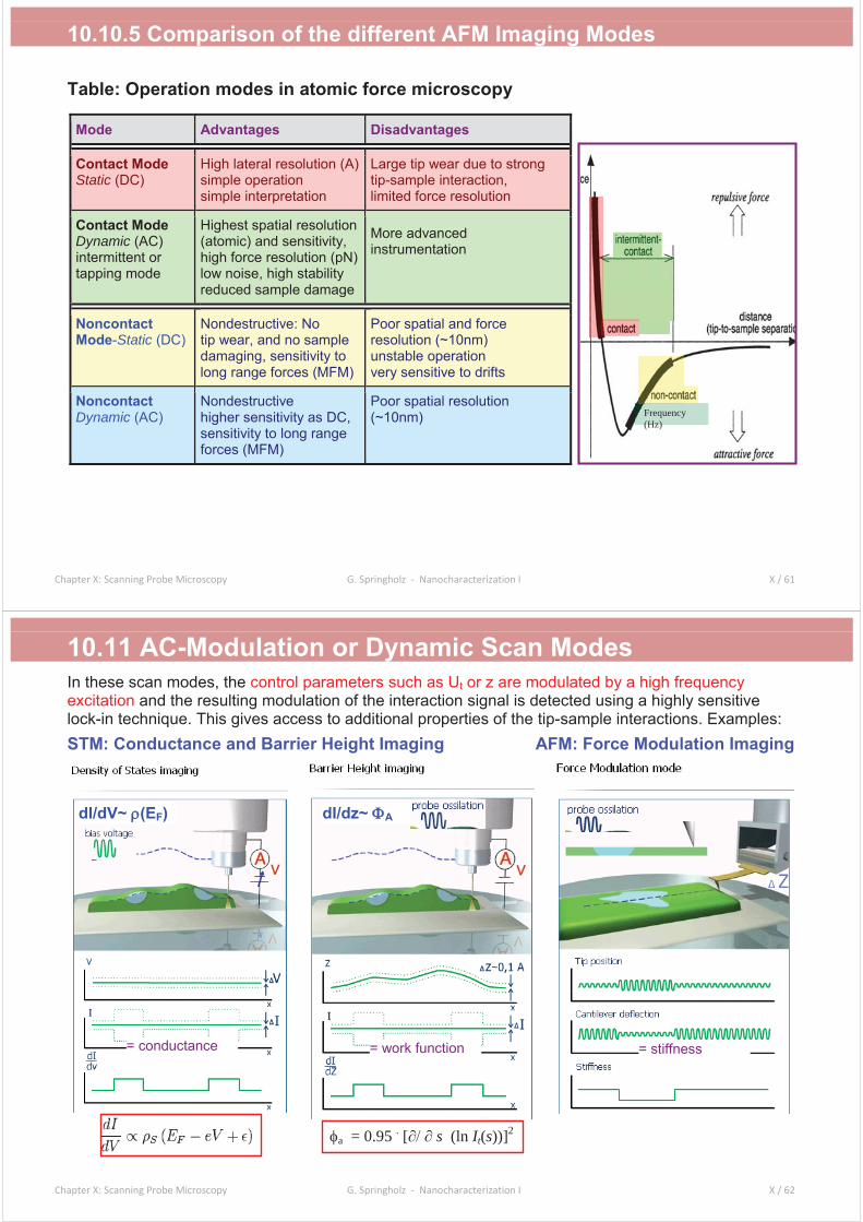
10.10.3 Oscillation Detection Modes: Amplitude vs Frequency Detection
(a) Amplitude Detection: = Excitation at constant excitation frequency fexc close to fres
Measurement of amplitude change A using lock-in technique.
(b) Frequency modulation mode: = Excitation frequency is kept tuned to resonance and amplitude kept constant. Measurement of frequency change f relative to free-air resonance frequency
Chapter X: Scanning Probe Microscopy G. Springholz - Nanocharacterization I X / 60
NC-ModeTapping
Mode
10.10.4 Intermittent Contact (Tapping) versus Non-Contact Mode
Tapping mode (= intermittent contact) AFMIn this operation mode, the excitation fre-quency is set slightly below the resonancefrequency of the free cantilever and the amplitude set-point for scanning at a value lower than the amplitude of the free cantilever at the excitation frequency. As the tip comes into the contact regime (tapping on the sample), the resonance curve shifts to the right hand side to higher frequencies and thus, the cantilever amplitude at the drive frequency is reduced until the set-point value is reached.
Non-contact mode (far distance attractive force regime)In NC-mode AFM, the excitation frequency is set slightly above the resonance frequency of the free cantilever and the amplitude set-point for scanning at a value lower than the amplitude of the free cantilever at this excitation frequency. As the tip comes in the non-contact regime, the resonance curve shifts to the left hand side to lower frequencies because the attractive force retards the cantilever oscillation. Thus, at the fixed excitation frequency, the cantilever amplitude is reduced until the set-point value is reached.
dynamic
zFts /
)(zFts
Force and force gradient in AFM
*z
Chapter X: Scanning Probe Microscopy G. Springholz - Nanocharacterization I X / 61
10.10.5 Comparison of the different AFM Imaging Modes
Table: Operation modes in atomic force microscopy
Mode Advantages Disadvantages
Contact ModeStatic (DC)
High lateral resolution (A)simple operationsimple interpretation
Large tip wear due to strong tip-sample interaction,limited force resolution
Contact ModeDynamic (AC)intermittent or tapping mode
Highest spatial resolution (atomic) and sensitivity, high force resolution (pN)low noise, high stabilityreduced sample damage
More advanced instrumentation
Noncontact Mode-Static (DC)
Nondestructive: Notip wear, and no sample damaging, sensitivity to long range forces (MFM)
Poor spatial and force resolution (~10nm)unstable operationvery sensitive to drifts
Noncontact Dynamic (AC)
Nondestructivehigher sensitivity as DC, sensitivity to long range forces (MFM)
Poor spatial resolution (~10nm) Frequency
(Hz)
Chapter X: Scanning Probe Microscopy G. Springholz - Nanocharacterization I X / 62
10.11 AC-Modulation or Dynamic Scan Modes In these scan modes, the control parameters such as Ut or z are modulated by a high frequency excitation and the resulting modulation of the interaction signal is detected using a highly sensitive lock-in technique. This gives access to additional properties of the tip-sample interactions. Examples:STM: Conductance and Barrier Height Imaging AFM: Force Modulation Imaging
= conductance
dI/dV~ (EF) dI/dz~ A
a = 0.95 . [ s (ln It(s))]2
= work function = stiffness
Chapter X: Scanning Probe Microscopy G. Springholz - Nanocharacterization I X / 63
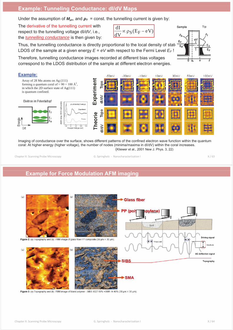
Example: Tunneling Conductance: dI/dV Maps
Under the assumption of M , and T = const. the tunnelling current is given by: The derivative of the tunnelling current with respect to the tunnelling voltage dI/dV, i.e., the tunnelling conductance is then given by:Thus, the tunnelling conductance is directly proportional to the local density of states LDOS of the sample at a given energy E = eV with respect to the Fermi Level EF !
Therefore, tunnelling conductance images recorded at different bias voltages correspond to the LDOS distribution of the sample at different electron energies.
Example: Array of 28 Mn atoms on Ag (111)
2,in which the 2D surface state of Ag(111)is quantum confined.
Imaging of conductance over the surface, shows different patterns of the confined electron wave function within the quantum coral: At higher energy (higher voltage), the number of nodes (minima/maxima in dI/dV) within the coral increases.
(Kliewer et al., 2001 New J. Phys. 3, 22)
)eVE(dVdI
FS
Chapter X: Scanning Probe Microscopy G. Springholz - Nanocharacterization I X / 64
Example for Force Modulation AFM imaging
Chapter X: Scanning Probe Microscopy G. Springholz - Nanocharacterization I X / 65
10.12 Hybrid Scan ModesIn hybrid scan modes, several interactions are measured simultaneously during imaging process.One interaction signal (typically the force or tunneling current) is used to keep the tip at a constant height / separation. The other interaction signals at this constant separation are used to measure local physical properties of the sample such as frictional force, capacitance, conductance, etc. :
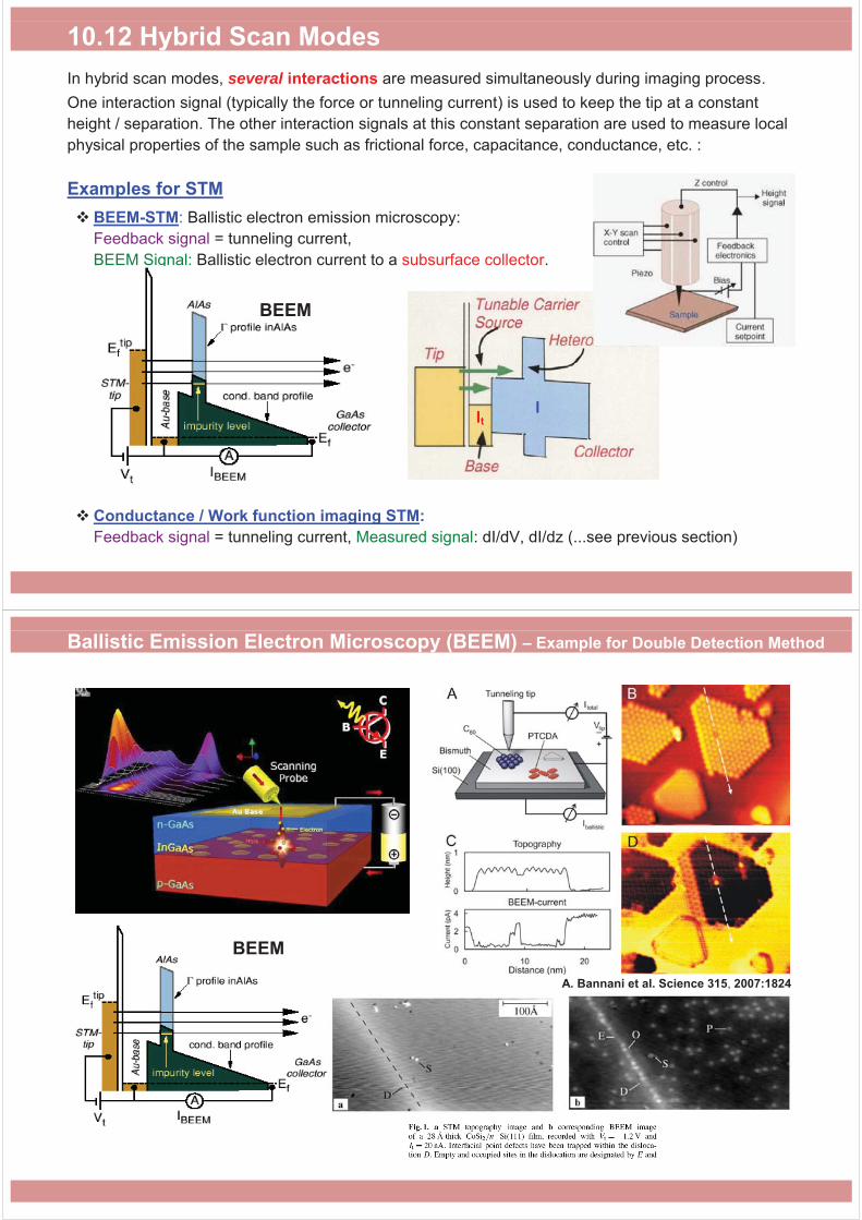
Examples for STMBEEM-STM: Ballistic electron emission microscopy: Feedback signal = tunneling current, BEEM Signal: Ballistic electron current to a subsurface collector.
Conductance / Work function imaging STM:Feedback signal = tunneling current, Measured signal: dI/dV, dI/dz (...see previous section)
ItI
BEEM
Chapter X: Scanning Probe Microscopy G. Springholz - Nanocharacterization I X / 66
Ballistic Emission Electron Microscopy (BEEM) – Example for Double Detection Method
A. Bannani et al. Science 315, 2007:1824
BEEM
Chapter X: Scanning Probe Microscopy G. Springholz - Nanocharacterization I X / 67
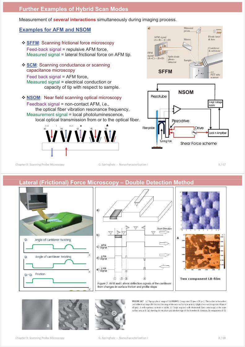
Further Examples of Hybrid Scan Modes
Measurement of several interactions simultaneously during imaging process.
Examples for AFM and NSOM
SFFM: Scanning frictional force microscopyFeed-back signal = repulsive AFM force, Measured signal = lateral frictional force on AFM tip.
SCM: Scanning conductance or scanning capacitance microscopyFeed back signal = AFM force, Measured signal = electrical conduction or
capacity of tip with respect to sample.
NSOM: Near field scanning optical microscopyFeedback signal = non-contact AFM, i.e.,
the optical fiber vibration resonance frequency, Measurement signal = local photoluminescence,
local optical transmission from or to the optical fiber.
NSOM
SFFM
Chapter X: Scanning Probe Microscopy G. Springholz - Nanocharacterization I X / 68
Lateral (Frictional) Force Microscopy – Double Detection Method
Chapter X: Scanning Probe Microscopy G. Springholz - Nanocharacterization I X / 69
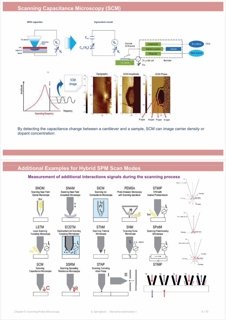
Scanning Capacitance Microscopy (SCM)
By detecting the capacitance change between a cantilever and a sample, SCM can image carrier density or dopant concentration.
Chapter X: Scanning Probe Microscopy G. Springholz - Nanocharacterization I X / 70
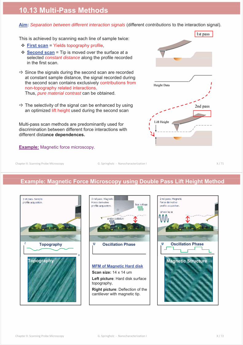
Additional Examples for Hybrid SPM Scan ModesMeasurement of additional interactions signals during the scanning process
Chapter X: Scanning Probe Microscopy G. Springholz - Nanocharacterization I X / 71
10.13 Multi-Pass Methods
Aim: Separation between different interaction signals (different contributions to the interaction signal).
This is achieved by scanning each line of sample twice: First scan = Yields topography profile,Second scan = Tip is moved over the surface at a selected constant distance along the profile recorded in the first scan.
Since the signals during the second scan are recorded at constant sample distance, the signal recorded during the second scan contains exclusively contributions from non-topography related interactions.Thus, pure material contrast can be obtained.
The selectivity of the signal can be enhanced by using an optimized lift height used during the second scan
Multi-pass scan methods are predominantly used for discrimination between different force interactions with different distance dependences.
Example: Magnetic force microscopy.
Chapter X: Scanning Probe Microscopy G. Springholz - Nanocharacterization I X / 72
Example: Magnetic Force Microscopy using Double Pass Lift Height Method
MFM of Magnetic Hard diskScan size: 14 x 14 umLeft picture: Hard disk surface topography, Right picture: Deflection of the cantilever with magnetic tip.
Topography Magnetic Structure
Oscillation Phase Oscillation PhaseTopography
Chapter X: Scanning Probe Microscopy G. Springholz - Nanocharacterization I X / 73
Magnetic Force Microscopy (MFM)
MFM simultaneously measures both topography and magnetic properties of sample. Using a cantilever coated with magnetized metal layer, spatial variation of magnetic domains can be observed, which gives more information than optical measurement such as magneto-optical Kerr effect.
Chapter X: Scanning Probe Microscopy G. Springholz - Nanocharacterization I X / 74
10.14 Summary1. In scanning probe microscopy, the surface of a sample is scanned with a microsco-
pically sharp probe tip at a distance of 1... 50 Å away from the surface. The tip-sample distance is controlled by measuring the strength of the tip-sample interaction.
2. Several different types of interactions occur between the tip and sample surface: Quantum mechanical, repulsive / attractive forces, dipolar & van der Waals forces, tunneling, etc. . The type of utilized interaction determines the SPM technique. Main techniques: Scanning Tunneling Microscopy (STM), Scanning (Atomic) Force Microscopy (SFM/AFM), Scanning Near Field Optical Microscopy (SNOM).Image contrast: Depends on the type of tip – sample interaction.
3. Resolution: Sub-Å resolution possible. Not determined by diffraction effects but only by the tip-sample interaction as well as by the radius of the scanning tip. Atomic resolution is obtained only for clean and well prepared sample surfaces and SPM tips.
4. Different scan modes exist: Constant height, constant interaction, DC / AC interaction modes, hybrid modes. 3D topography reconstruction by constant interaction mode.
5. Feedback loops of the SPM systems use a Proportional – Integral – Derivative control system to minimize the error signal of the detector and to regulate the tip-sample distance during the scanning process.
Chapter X: Scanning Probe Microscopy G. Springholz - Nanocharacterization I X / 75
Chapter X: Scanning Probe Microscopy G. Springholz - Nanocharacterization I X / 76
Appendix
Literature and History ofScanning Probe Microscopy
Chapter X: Scanning Probe Microscopy G. Springholz - Nanocharacterization I X / 77
Literature1. Scanning Probe Microscopy, E. Meyer, H.J. Hug and R. Bennewitz, Springer Verlag (2004).
2. Scanning Probe Microscopy and Spectroscopy, R. Wiesendanger, Chambridge Univ. Press (1994).3. Noncontact Atomic Force Microscopy S. Morita, R. Wiesendanger and E. Meyer, Springer (2002).4. Introduction to Scanning Tunneling Microscopy, C.J. Chen, Oxford U. Press (1993).5. Scanning Tunneling Microscopy, eds. J. A. Stroscio and W. J. Kaiser, Methods in Experimental Physics,
Vol. 27, Academic Press (1993).6. Scanning Tunneling Microscopy and its Applications, Chunli Bai, Springer (1992).7. Scanning Tunneling Microscopy and Spectroscopy, D. A. Bonell, VCH (1993).8. Raster Tunnel Mikroskopie, C. Haman und M. Hietschold, Akademie Verlag (1991).9. Scanning Tunneling Microscopy I - III, eds. R. Wiesendanger and H. J. Güntherrodt, Springer (1994).10. Nanoscale Characterization of Surfaces and Interfaces, N. J. DiNardo, VCH Verlag (1994).11. Scanning Force Microscopy with Applications to Electric, Magnetic and Atomic Force,
D. Sarid, Oxford Univ. Press (1992).12. Near Field Optics: Theory, Instrumentation and Applications, M. Paesler and P.J. Moyer, John Wiley
(1996).
Review articles:
13. Scanning Tunneling Microscopy and Related Methods, eds. R. J. Behm, N. Garcia and H. Rohrer, Kluwer Academic Press (1990).
14. IBM Journal of Research and Development, Vol. 30/4 (1996).
Chapter X: Scanning Probe Microscopy G. Springholz - Nanocharacterization I X / 78
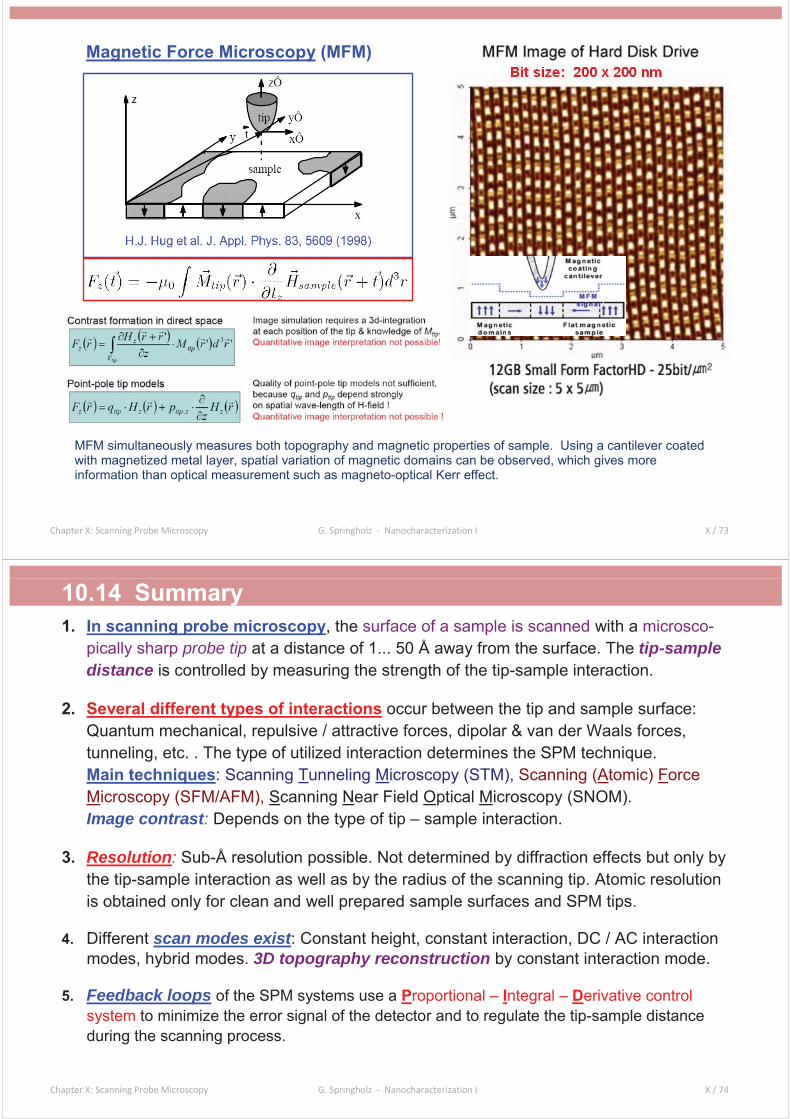
The History of Scanning Probe Microscopy(i) Forerunners
• Topographiner (R. Young et al., NIST, 1972): Microscope measuring the field emission from a tip to a sample at a distance of several 100 Å. In scanning mode, lateral resolution of about 20 nm and of ~3 nm in vertical direction. Problems with mechanical instabilities.
• Stylus-profilometer for measuring surface profiles and layer thicknesses. Mechanical scanning of a hard tip over a sample with no good lateral resolution. But: No significant influence on the further development!
Chapter X: Scanning Probe Microscopy G. Springholz - Nanocharacterization I X / 79
(ii) Invention of the scanning tunneling microscope
by G. Binning and H. Rohrer (IBM Research Lab in Rüschlikon,CH) together with C. Gerber and E. Weibel).
Original research direction (starting 1979):
Aim: Local tunneling spectroscopy of thin oxide layers to overcome the problems caused by inhomogenous thickness and defects in MOS oxide layers used in semiconductor devices.Task: Develop an instrument based on the idea of vacuum tunneling through a very thin gap between the probing tip and the sample.
In order to be able to record tunneling spectra at different position on the surface, a means to position the tip laterally on the surface was required.
=> Scanning the tip over the sample immediately resulted in the possibility to obtain information on the sample topography and thus to use this instrument for microscopy !
Chapter X: Scanning Probe Microscopy G. Springholz - Nanocharacterization I X / 80
Problems that had to be solved:
Sub-Å stability of tunneling gap against mechanical vibrations from the surrounding environment» solved by rigid mechanical design of STM head and by spring suspension and eddy current damping,movement and positioning of the tip over the sample with sub-Angstrom precision, » solved by using piezoelectric positioning elements,macroscopic and well-controlled approach of the tip and sample into the Å regime where a tunneling current appears: » solved by “louse” walkerPreparation of sharp and clean STM tips and clean surfaces: UHV system
Instrumental developments by Binning, Rohrer, Gerber und Weibel:
First (not working) prototype: low-temperature STM with superconducting levitation damping
After 2 years development time:
1981: first UHV compatible STM system with spring suspension
Chapter X: Scanning Probe Microscopy G. Springholz - Nanocharacterization I X / 81
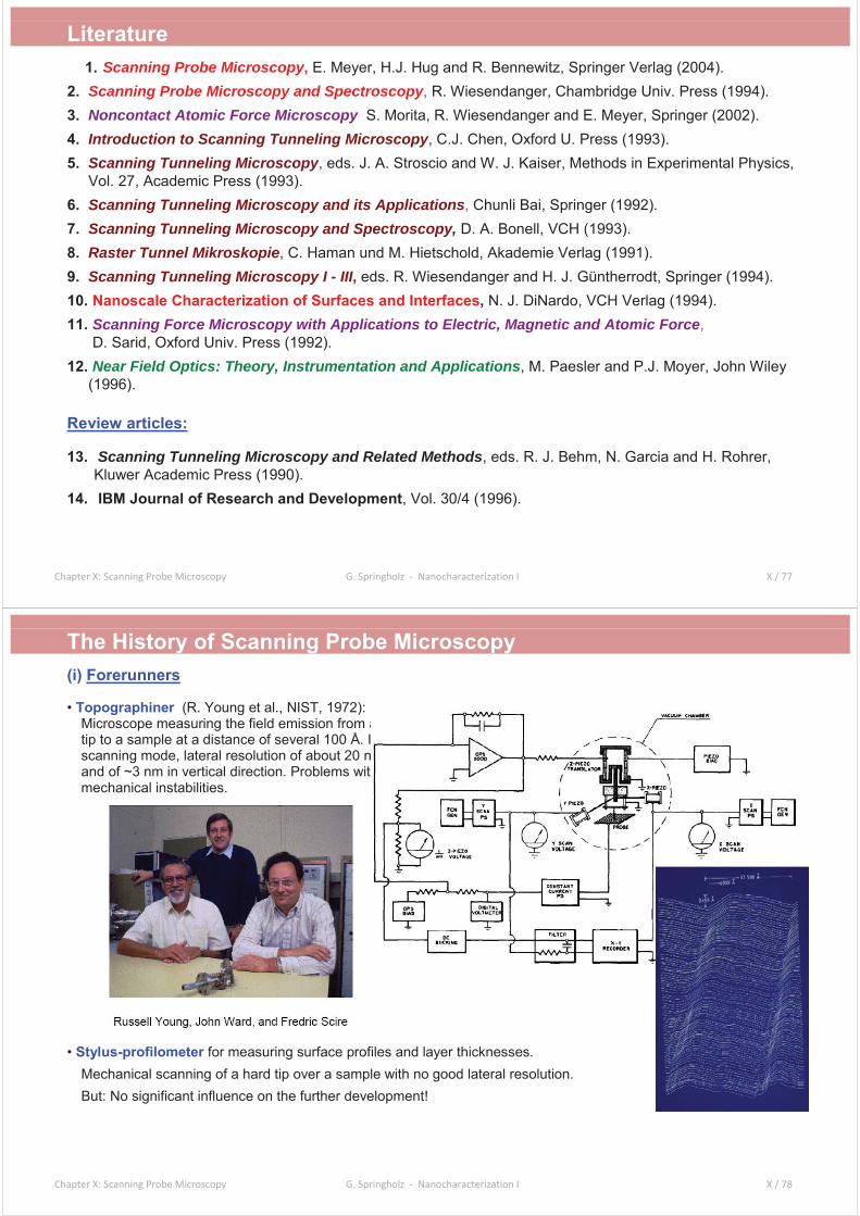
Timeline1981: First well-defined tunneling measurements (see Fig. below) of
exponential dependence of the tip-sample current versus distance during the night time. First topographic images of surfaces with resolution of single monoatomic surface steps(Gold (110) and CaIrSn4 (110)) but no lateral atomic resolution.
First atomic resolution for 2x1 reconstructed Au(110) surface (unpublished) but measurements still unstable
Okt. 1982: Breakthrough with resolution of the atomic structure of Si(111) 7x7 surface reconstruction.
Additional experiments: Atomic resolution of the O2 - induced (2 x 1) reconstruction of the Ni (110) surface and of the (2 x 2 ) reconstruction of the Ni(100) surface, surface reconstructions of Au and of Au on Si (111).1983: First STM imaging of DNA chains.
Chapter X: Scanning Probe Microscopy G. Springholz - Nanocharacterization I X / 82
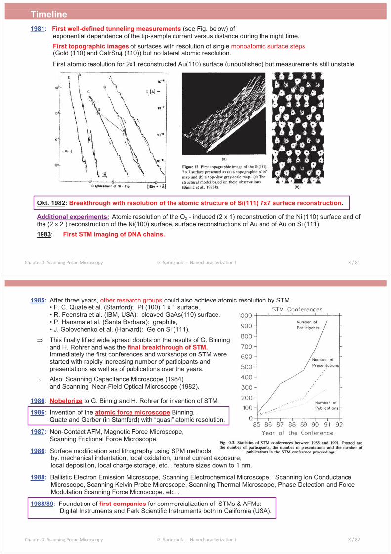
1985: After three years, other research groups could also achieve atomic resolution by STM. • F. C. Quate et al. (Stanford): Pt (100) 1 x 1 surface,• R. Feenstra et al. (IBM, USA): cleaved GaAs(110) surface.• P. Hansma et al. (Santa Barbara): graphite,• J. Golovchenko et al. (Harvard): Ge on Si (111).This finally lifted wide spread doubts on the results of G. Binning and H. Rohrer and was the final breakthrough of STM. Immediately the first conferences and workshops on STM were started with rapidly increasing number of participants and presentations as well as of publications over the years.Also: Scanning Capacitance Microscope (1984) and Scanning Near-Field Optical Microscope (1982).
1986: Nobelprize to G. Binnig and H. Rohrer for invention of STM.
1986: Invention of the atomic force microscope Binning, Quate and Gerber (in Stamford) with “quasi” atomic resolution.
1987: Non-Contact AFM, Magnetic Force Microscope, Scanning Frictional Force Microscope,
1986: Surface modification and lithography using SPM methods by: mechanical indentation, local oxidation, tunnel current exposure, local deposition, local charge storage, etc. . feature sizes down to 1 nm.
1988: Ballistic Electron Emission Microscope, Scanning Electrochemical Microscope, Scanning Ion Conductance Microscope, Scanning Kelvin Probe Microscope, Scanning Thermal Microscope, Phase Detection and Force Modulation Scanning Force Microscope. etc. .
1988/89: Foundation of first companies for commercialization of STMs & AFMs: Digital Instruments and Park Scientific Instruments both in California (USA).
Chapter X: Scanning Probe Microscopy G. Springholz - Nanocharacterization I X / 83
1990: Manipulation of single atoms of Xe on Ni (110), Eigler&Schweitzer (1990, IBM)
1996: True atomic resolution with AFM demonstrated for Si (111) by Giessibl et al.,
1993: Imaging of Surface Electronic Wave FunctionsExample: Surface State Waves on Ag (111) at T=5KStanding surface state waves around two surface defects on a Ag(111) film grown on HOPG imaged with LT STM at T = 5 K in the constant-current mode.
Left images show the standing waves (upper image)and the topography (lower image). The hole defect and the adatom defect lead to distinct differences in the centre of the two circular waves which exhibit pronounced interference effects.
References :1. M. F. Crommie, C. P. Lutz, and D. M. Eigler, Nature 363, 524 (1993).2. Y. Hasegawa and Ph. Avouris, Phys. Rev. Lett. 71, 1071 (1993). 3. J. Li, W. D. Schneider, and R. Berndt, Phys. Rev. B. 56, 7656 (1997).
nctions
e fects.
93).
997)
Example: Atomic Resolution of Si(111) 7 x 7 in UHV(a) STM: U = 2 V, I = 2.0 nA, (b) Non-Contact Mode AFM, (c) Multi-mode operation:
simultaneous measurement of the topography in STM mode using a conductive cantilever, and of the atomic scale variation of the force, i.e. cantilever deflection.
(a) STM (b) NC-AFM (c)
AFMSTM
Ag(111)
topo
con-ductance
Chapter X: Scanning Probe Microscopy G. Springholz - Nanocharacterization I X / 84
Present Day Status ~20 different commercial producers of SPMs:
Frequent mergers and take-overs: Bruker = Veeco + Digital Instrument + ThermoMicroscopes + Park Scientific Instruments + Topometrix,
Annual revenues: ~ 200 Mio € /year; corresponds to ~1000 SPM,number of instruments worldwide ~10.000 SPMs.
Application areas:
Research and development: Physics, chemistry, material science, biology, medicine, mechanical and electrical engineering in universities as well as industrial research labs and production.
Materials: Semiconductors, ceramics, metals, magnetic materials, polymers, bio-systems, soft matter, Industry: semiconductor and microelectronics industry, CD and magnetic data storage industry, optical industry, coating industry, materials, chemical and pharmaceutical industry, medical diagnostics, hospitals,
Nanotechnology: Nanoanalysis and Microscopy, Nanofabrication and Manipulation, ......