Partial Reconfiguration: A Simple Tutorial Richard Neil Pittman Microsoft Research February 2012 Technical Report MSR-TR 2012-19 Microsoft Research Microsoft Corporation One Microsoft Way Redmond, WA 98052
Transcript
Partial Reconfiguration: A Simple Tutorial
Richard Neil Pittman
Microsoft Research
February 2012
Technical Report
MSR-TR 2012-19
Microsoft Research
Microsoft Corporation
One Microsoft Way
Redmond, WA 98052
Partial Reconfiguration: A Simple Tutorial
A Tutorial for XILINX FPGAs
Neil Pittman – 2/12, version 1.0
Introduction Partial Reconfiguration is a feature of modern FPGAs that allows a subset of the logic fabric of a FPGA to
dynamically reconfigure while the remaining logic continues to operate unperturbed. Xilinx has
provided this feature in their high end FPGAs, the Virtex series, in limited access BETA since the late
1990s. More recently it is a production feature supported by their tools and across their devices since
the release of ISE 12. The support for this feature continues to improve in the more recent release of
ISE 13. Altera has promised this feature for their new high end devices, but this has not yet
materialized.
Partial Reconfiguration of FPGAs is a compelling design concept for general purpose reconfigurable
systems for its flexibility and extensibility. Despite the significant improvements in software tools and
support, the Xilinx partial reconfiguration design option has a reputation for being an expert level flow
that is difficult to use. In this tutorial we will show that it can actually be quite simple. As a case study,
we apply Partial Reconfiguration to the Simple Interface for Reconfigurable Computing (SIRC) toolset.
Combining SIRC and partial reconfiguration makes the idea of general purpose hardware and software
user systems deployed on demand on generic platforms viable. The goal is to make developers more
confident in the practicality of this concept and in their own ability to use it, so that more will take
advantage of what it has to offer.
Prerequisites Before beginning there are some prerequisites for successfully completing the tutorial.
A working knowledge of the Xilinx IDE is required to understand and successfully complete this tutorial.
You must have at least version 12 of the Xilinx Integrated Development Environment (IDE), including ISE
and PlanAhead. It is recommended that you have the latest version available. For this tutorial, all
screenshots and procedures will be performed using version 13.2 of the IDE. In addition, the partial
reconfiguration design flow requires an additional license to activate the feature in the tools. Please
contact for Xilinx representative for assistance in acquiring such a license.[6]
This tutorial requires the latest version of the SIRC hardware/software API. For this tutorial, the
hardware and software sources are derived from SIRC release 1.1.[1]
The partial reconfiguration feature as presented in this tutorial is supported the Xilinx Virtex series since
the Virtex 4 and in the Spartan series since Spartan 6. All the Xilinx 7 series FPGAs support partial
reconfiguration. In this tutorial, the system will be designed and implemented on a Virtex 6 LX 240t
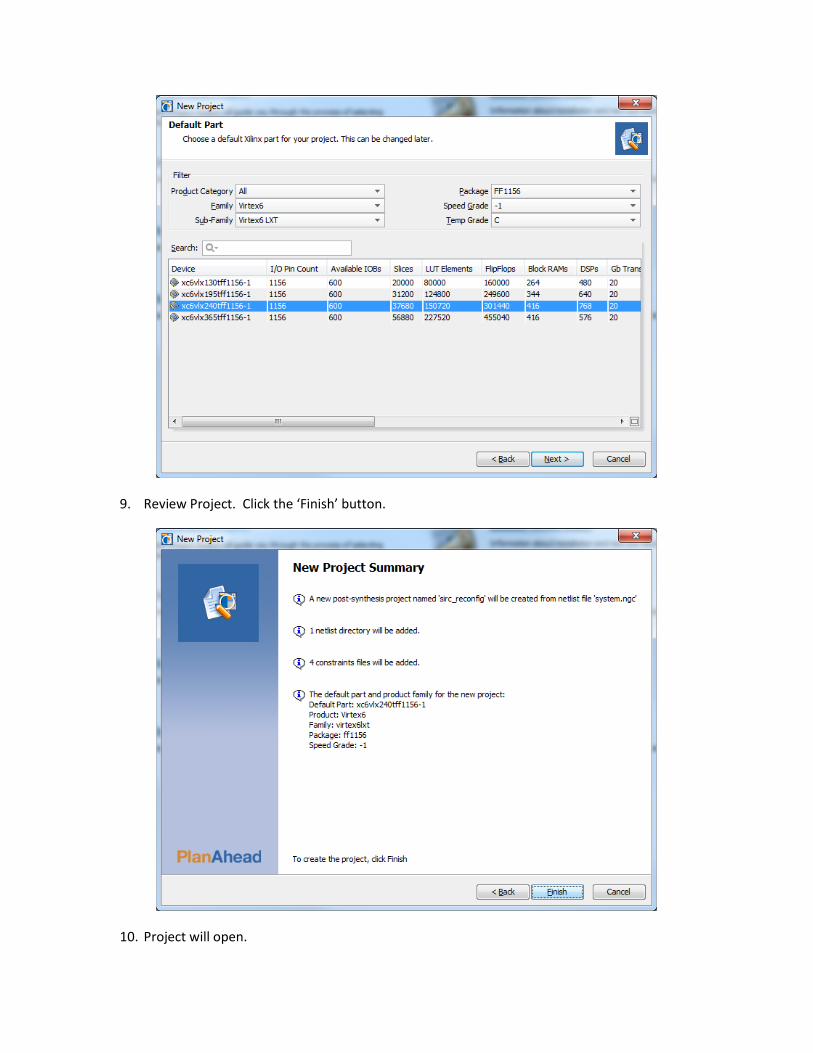
(xc6vlx240t-1ff1156) on a Xilinx ML605 evaluation board.[3]
Generalities The regular synthesis flow generates a single bitstream for programming the FPGA. This considers the
device as a single atomic entity. In contrast, the PR flow physically divides the device in regions. One
region is called the “static region”, which is the portion of the device that is programmed at startup and
never changes. One region is the “dynamic region” aka “the PR region”, which is the portion of the
device that will be reconfigured dynamically, potentially multiple times and with different designs. It is
possible to have multiple PR regions, but we will consider only the simplest case here.[4]
The PR flow generates at least two bitstreams, one for the static and one for the PR region. Most likely,
there will be multiple PR bitstreams, one for each design that can be dynamically loaded. In our case, we
place the basic SIRC functionality into the static region. The user circuits instead go into the PR region.
Another practical example is an FPGA board where we place the PCIe interface logic in a static region of
the FPGA and the user circuits in the PR region. This eliminates the need for a full-device reset on each
separate application run, with potentially negative effects on the OS.
The PR region is a physical entity, with a given geometry. PlanAhead is the tool that allows you to define
the exact location of the PR region on your target device. [4]
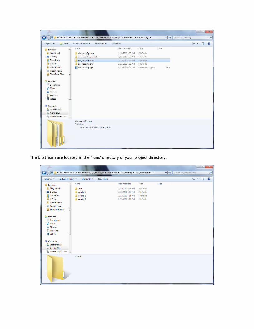
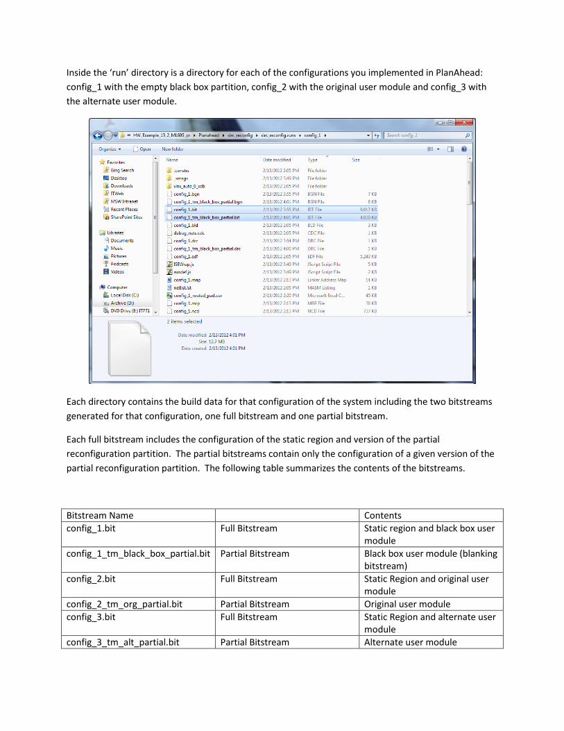
Building SIRC with Partial Reconfiguration
Synthesis The first step in implementing a system using the Xilinx partial reconfiguration design flow is to
synthesize the netlists from the HDL sources that will be used in the implementation process. The
process requires separate netlists for the static (top level) design and for the partial reconfigurable
partition(s). A netlist must be generated for each implementation of the partial reconfiguration
partition used in the design. If the system design has multiple partial reconfiguration partitions, then it
will require a netlists for each implementation of each partial reconfiguration partition, even if the logic
is the same in multiple locations.
First, you should create a new directory to hold the synthesis files and name it appropriately. We will
use ‘Synthesis’ in this tutorial. This folder will eventually contain several separate synthesis projects for
each of the netlists that the design requires for implementation. Then proceed to next section to begin
implementing the netlists for the SIRC example. The SIRC release like many other designs uses of some
ip cores generated by CoreGen. These ip cores are included in the design as netlists rather than source.
These will also be required in the implementation process.
Synthesizing the Static Region
1. Create a new folder inside the Synthesis Folder and label it ‘Static’
2. Inside that Folder, create a new ISE project.
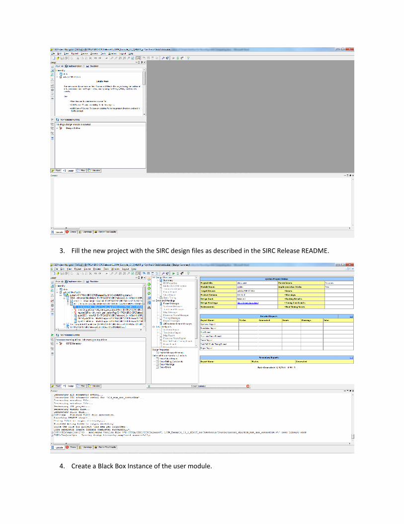
3. Fill the new project with the SIRC design files as described in the SIRC Release README.
4. Create a Black Box Instance of the user module.
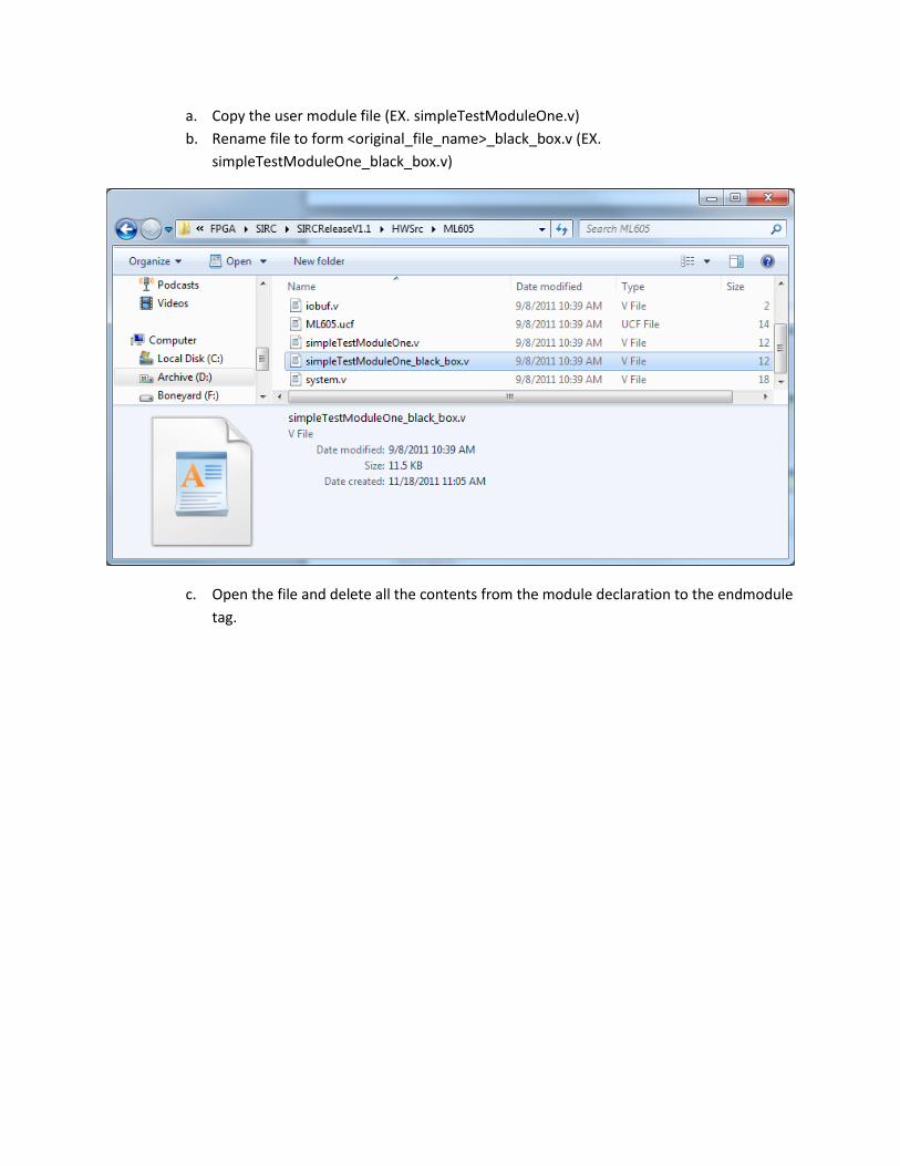
a. Copy the user module file (EX. simpleTestModuleOne.v)
b. Rename file to form <original_file_name>_black_box.v (EX.
simpleTestModuleOne_black_box.v)
c. Open the file and delete all the contents from the module declaration to the endmodule
tag.
5. Remove the original user module from the project (EX. simpleTestModuleOne.v)
6. Replace the user module file with the black box (EX. simpleTestModuleOne_black_box.v)
7. Synthesize the static design.
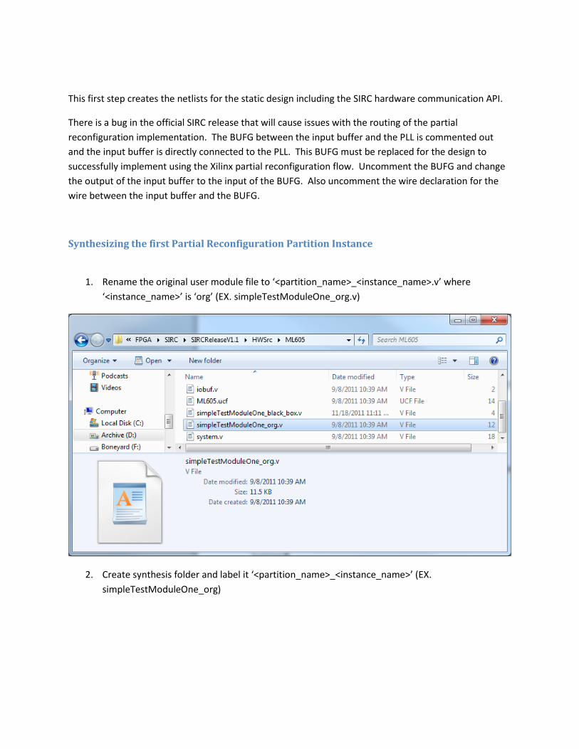
This first step creates the netlists for the static design including the SIRC hardware communication API.
There is a bug in the official SIRC release that will cause issues with the routing of the partial
reconfiguration implementation. The BUFG between the input buffer and the PLL is commented out
and the input buffer is directly connected to the PLL. This BUFG must be replaced for the design to
successfully implement using the Xilinx partial reconfiguration flow. Uncomment the BUFG and change
the output of the input buffer to the input of the BUFG. Also uncomment the wire declaration for the
wire between the input buffer and the BUFG.
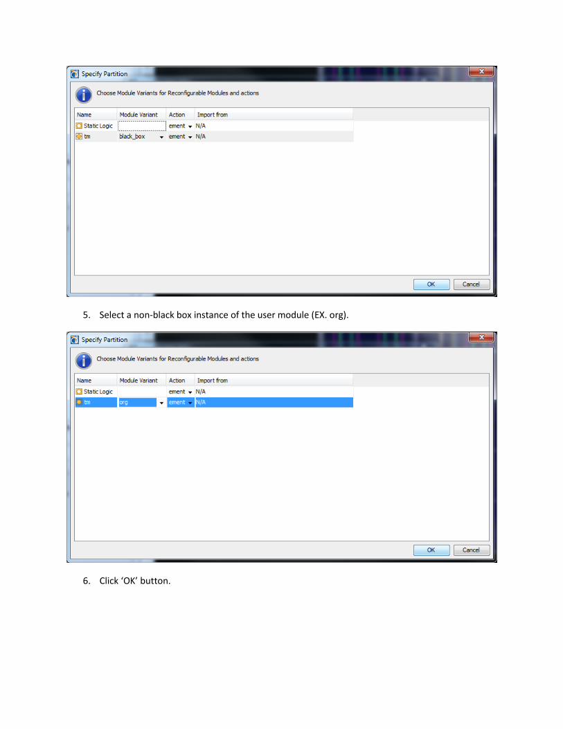
Synthesizing the first Partial Reconfiguration Partition Instance
1. Rename the original user module file to ‘<partition_name>_<instance_name>.v’ where
‘<instance_name>’ is ‘org’ (EX. simpleTestModuleOne_org.v)
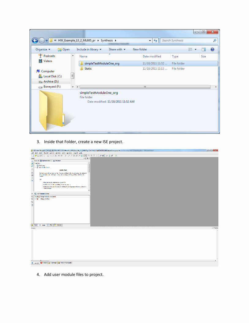
2. Create synthesis folder and label it ‘<partition_name>_<instance_name>’ (EX.
simpleTestModuleOne_org)
3. Inside that Folder, create a new ISE project.
4. Add user module files to project.
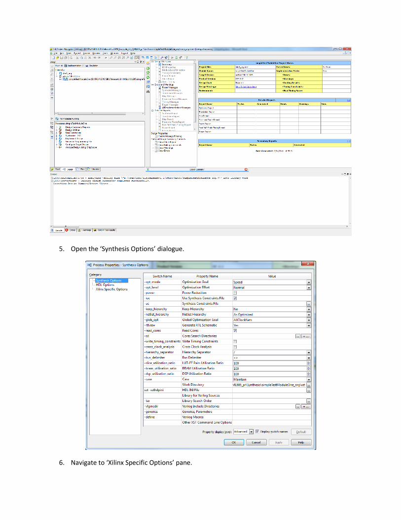
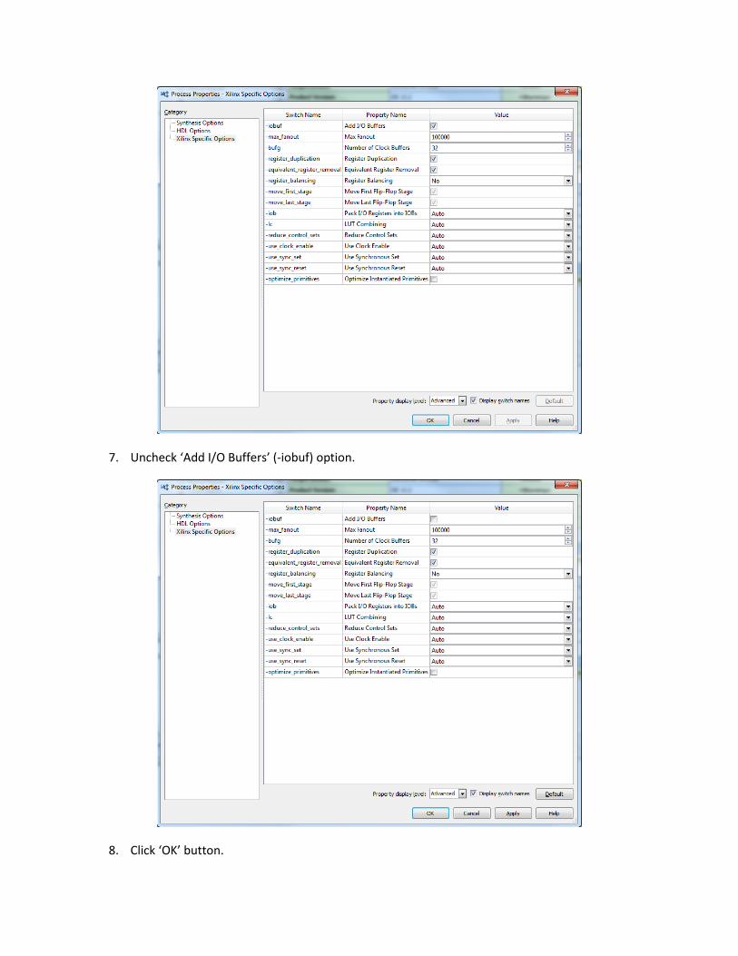
5. Open the ‘Synthesis Options’ dialogue.
6. Navigate to ‘Xilinx Specific Options’ pane.
7. Uncheck ‘Add I/O Buffers’ (-iobuf) option.
8. Click ‘OK’ button.
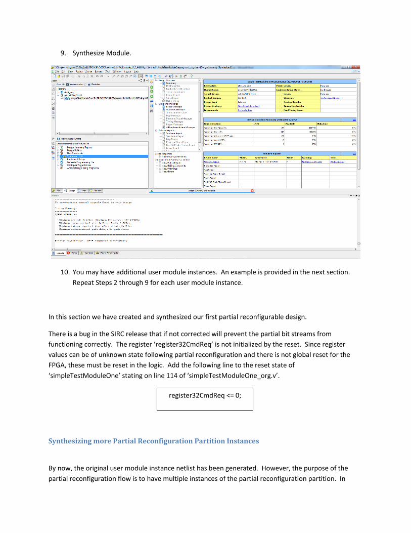
9. Synthesize Module.
10. You may have additional user module instances. An example is provided in the next section.
Repeat Steps 2 through 9 for each user module instance.
In this section we have created and synthesized our first partial reconfigurable design.
There is a bug in the SIRC release that if not corrected will prevent the partial bit streams from
functioning correctly. The register ‘register32CmdReq’ is not initialized by the reset. Since register
values can be of unknown state following partial reconfiguration and there is not global reset for the
FPGA, these must be reset in the logic. Add the following line to the reset state of
‘simpleTestModuleOne’ stating on line 114 of ‘simpleTestModuleOne_org.v’.
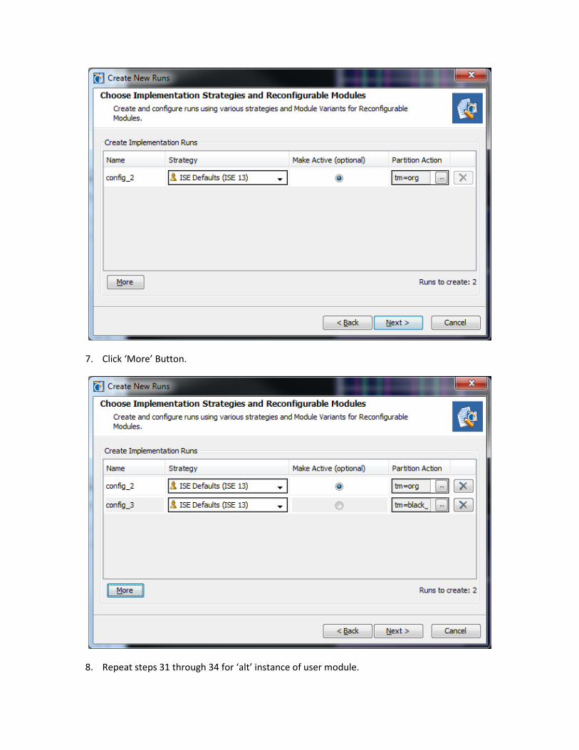
Synthesizing more Partial Reconfiguration Partition Instances
By now, the original user module instance netlist has been generated. However, the purpose of the
partial reconfiguration flow is to have multiple instances of the partial reconfiguration partition. In
register32CmdReq <= 0;
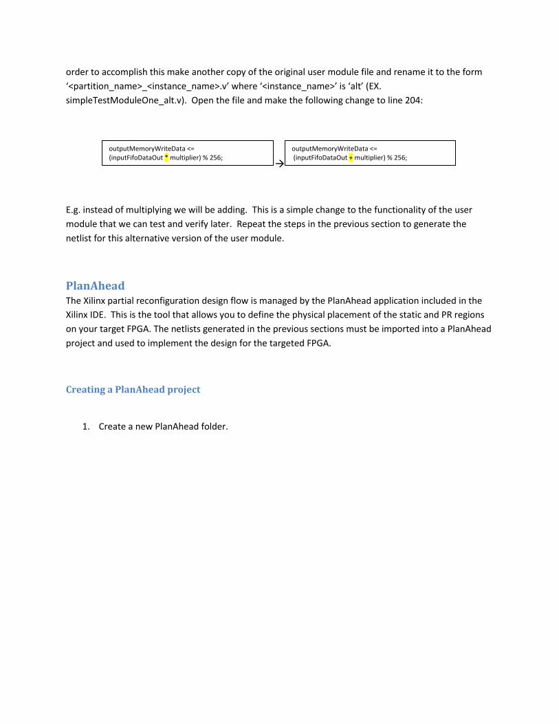
order to accomplish this make another copy of the original user module file and rename it to the form
‘<partition_name>_<instance_name>.v’ where ‘<instance_name>’ is ‘alt’ (EX.
simpleTestModuleOne_alt.v). Open the file and make the following change to line 204:
E.g. instead of multiplying we will be adding. This is a simple change to the functionality of the user
module that we can test and verify later. Repeat the steps in the previous section to generate the
netlist for this alternative version of the user module.
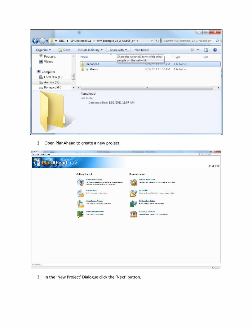
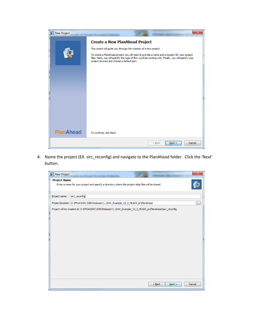
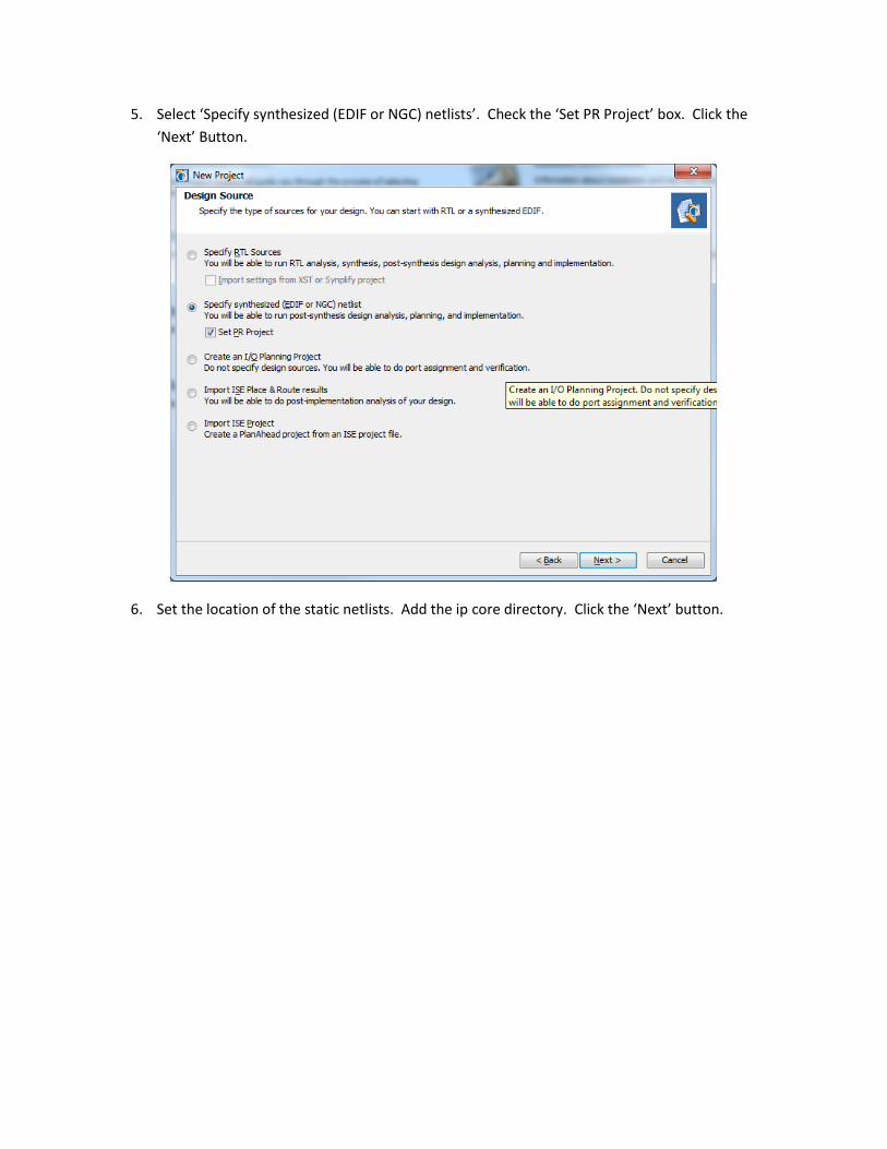
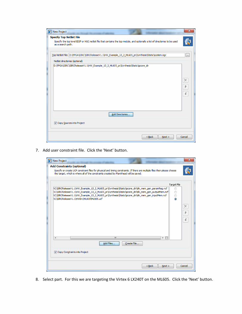
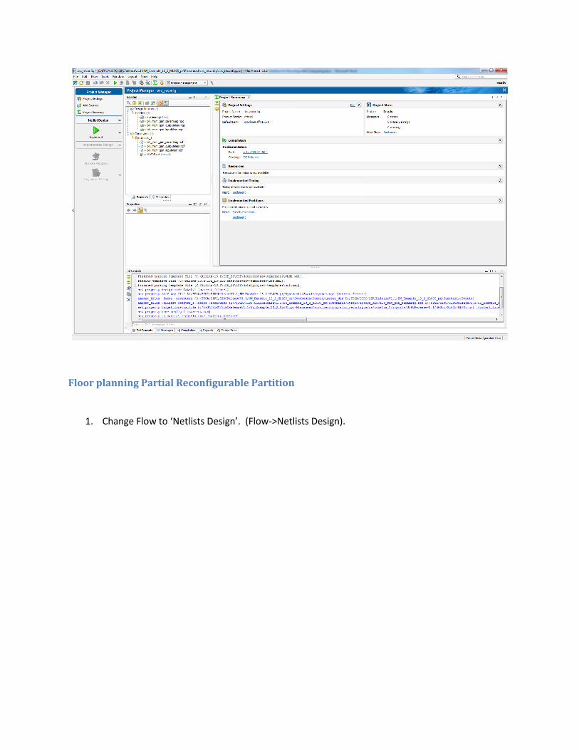
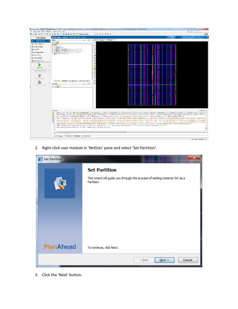
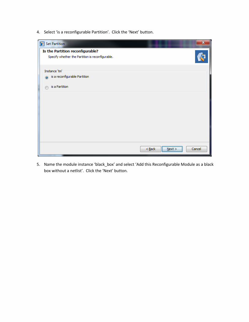
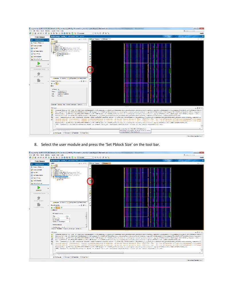
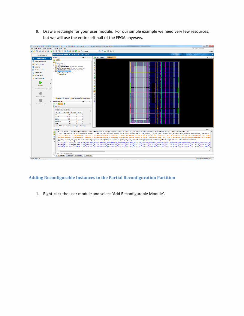
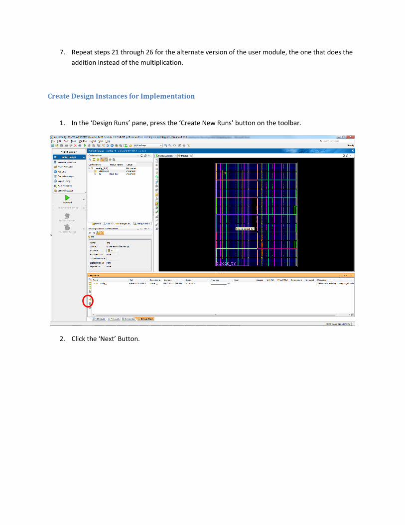
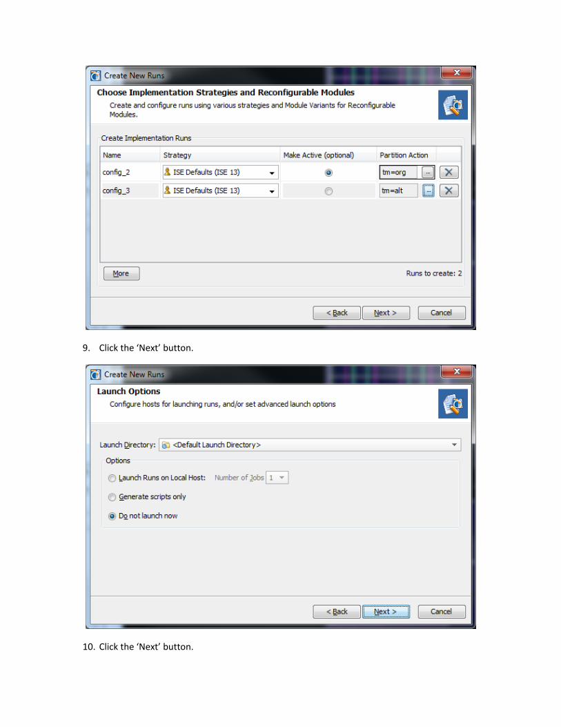
PlanAhead The Xilinx partial reconfiguration design flow is managed by the PlanAhead application included in the
Xilinx IDE. This is the tool that allows you to define the physical placement of the static and PR regions
on your target FPGA. The netlists generated in the previous sections must be imported into a PlanAhead
project and used to implement the design for the targeted FPGA.
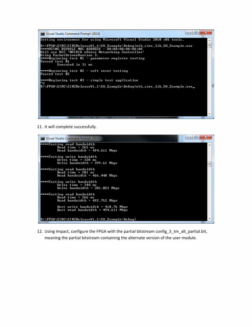
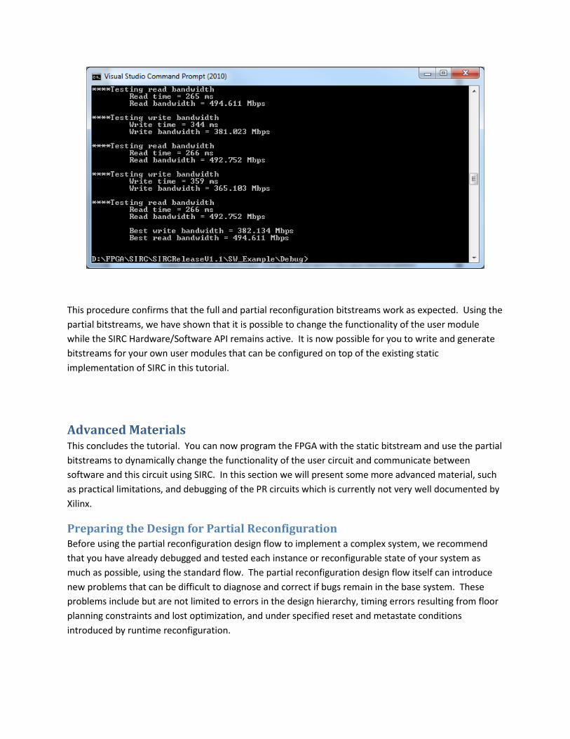
This procedure confirms that the full and partial reconfiguration bitstreams work as expected. Using the
partial bitstreams, we have shown that it is possible to change the functionality of the user module
while the SIRC Hardware/Software API remains active. It is now possible for you to write and generate
bitstreams for your own user modules that can be configured on top of the existing static
implementation of SIRC in this tutorial.
Advanced Materials This concludes the tutorial. You can now program the FPGA with the static bitstream and use the partial
bitstreams to dynamically change the functionality of the user circuit and communicate between
software and this circuit using SIRC. In this section we will present some more advanced material, such
as practical limitations, and debugging of the PR circuits which is currently not very well documented by
Xilinx.
Preparing the Design for Partial Reconfiguration Before using the partial reconfiguration design flow to implement a complex system, we recommend
that you have already debugged and tested each instance or reconfigurable state of your system as
much as possible, using the standard flow. The partial reconfiguration design flow itself can introduce
new problems that can be difficult to diagnose and correct if bugs remain in the base system. These
problems include but are not limited to errors in the design hierarchy, timing errors resulting from floor
planning constraints and lost optimization, and under specified reset and metastate conditions
introduced by runtime reconfiguration.
The first step in creating a system using partial reconfiguration from an existing static system, is
selecting what parts of the system you think should be able to reconfigure dynamically. When making
this decision, it is required that the functionality that you want to reconfigured be encapsulated within a
module. To simplify design and maintenance, functions that are intended to be changed together should
whenever possible be wrapped within the same higher level model to minimize the number of
independently reconfigurable partitions in the design. The complexity of the flow significantly increases
with additional partitions.
The Xilinx partial reconfiguration design flow imposes some restrictions on the contents of modules and
partitions meant to be reconfigured dynamically [4]. Most but not all components available within the
FPGA fabric can be included in a partial reconfiguration partition. Most of these exceptions are related
to clocking resources. All global clocking resources and those architectural features that are used to
modify clock signals cannot be included in a partial reconfiguration partition. These include BUFG,
MMCM, PLL and DCMs. Additionally architectural features related to configuration and FPGA state such
as BSCAN, STARTUP, ICAP, CAPTURE, DCIRESET, FRAME_ECC, KEY_CLEAR, USR_ACCESS, etc. cannot be
included in the partial reconfiguration partition. Additionally, any IP core that makes use of these
components may not be included in a partial reconfiguration partition. This includes some EDK blocks
and MIG. Under normal circumstances this would also preclude the use of Chipscope for debugging
within the partial reconfiguration partition because of the use of BUFGs and BSCAN components.
However we have a work around that will be presented later in this tutorial.
The Xilinx partial reconfiguration design flow also imposes restrictions on the interface to the partial
reconfiguration partition. Bidirectional ports on the interface between the partial reconfiguration
partition and the remaining design are not allowed. If the design makes the use of such ports they will
need to be separated into dedicated input and output ports and recombined into bidirectional ports
higher in the hierarchy. [4]
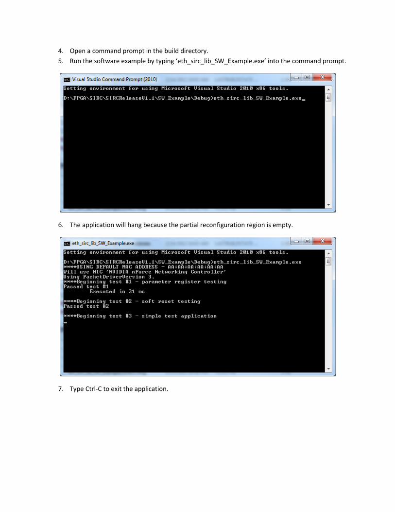
One major difference between a full configuration and a partial reconfiguration of the FPGA is that there
is no global reset of the logic after the configuration is complete. Thus the state of the logic in the
partial reconfiguration partition is unknown immediately following the completion of the
reconfiguration process. For this reason, all logic within the partial reconfiguration partition must be
initialized by a reset state and the partial reconfiguration partition should be reset after the
reconfiguration process and prior to resuming operation. Similarly, the state of partial reconfiguration
partition outputs will be of unknown state during the reconfiguration process. This process can take a
long period of clock cycles depending on the size partial reconfiguration partition and bandwidth of the
reconfiguration channel. For this reason, it is important to place the system into a safe state where the
outputs of the partial reconfiguration partition are ignored until the reconfiguration is complete and the
partition is reset. However, this does not preclude the remainder of the FPGA from operating on other
tasks that do not interact with the partial reconfiguration partition. [4]
The partial reconfiguration partition will be synthesized and implemented independently of the rest of
the design. This means that some optimizations that the tools took advantage of when the design was
flat will no longer apply now that these pieces are separated. In addition when you floor plan the design
later in the tutorial, you are imposing additional restrictions on the placement and routing of the design.
This in some cases is enough to push the timing of certain signals out of compliance and result in timing
errors. For this reason, additional pipeline stages as well as registering the inputs and output of partial
reconfiguration partitions is recommended to improve slack in the timing whenever possible. Xilinx
recommends expecting a 10% performance loss in clock frequency and expecting to not exceed 80% of
the FPGA resources. [4]
A big question when implementing a partial reconfiguration system relates to the floor planning. In
some cases, partial reconfiguration partitions will interact with fixed elements in the FPGA such as IO
pins and other features. It is possible to use these as anchors to guide the placement of the partial
reconfiguration partition in the floor plan. But what should be done when such anchors do not exist? A
good starting point is the original design implemented in the standard flow. If the standard flow placed
the logic in a certain area it is possible to constrain the partial reconfiguration to do the same, which will
provide similar results.
To view the location of a module on the FPGA in the design, locate the routed netlists or *.ncd file for
the design. Open that file in Xilinx FPGA Editor. Then search for the nets and components associated
with the module of the selected partial reconfiguration partition and highlight them. You will see a mass
of logic somewhere in the FPGA. If you are lucky, the mass will be fairly localized and you can aim to
place the region constraint for your partial reconfiguration centered on that mass. However, if the mass
is more widespread this may indicate that when partial reconfiguration flow is used timing and other
implementation issues may arise. In this case, more effort may be needed to better decouple the partial
reconfiguration partition from the design. Timing errors that surface later can also be dealt with using
timing constraints on the using partition pins of the partial reconfiguration partition.
Debugging Partial Reconfiguration Designs with Chipscope Chipscope is the on-chip debugging solution for Xilinx FPGAs. Using the Chipscope tool you can probe
signals of the design under development within the FPGA. The signal values are sampled each cycle of a
reference clock and stored in a provided blockram. Sampling begins when user defined trigger
conditions are satisfied until the allocated blockrams are filled. When the blockrams are filled the
captured data is sent to the host PC over the JTAG. Chipscope is well supported and partially automated
for non-partial reconfigurable designs, whereas using it with partial reconfiguration is not too well
supported. However, with some effort and knowledge it is possible to use Chipscope to debug designs
using partial reconfiguration. It is recommended though to do as much debugging and verification on a
non-partial reconfiguration version before moving to the partial reconfiguration flow.
Integrated Chipscope Support
Xilinx PlanAhead provides integrated support for setting up Chipscope probes for debugging. This works
similarly to the GUI based interface used in the ISE Project Navigator and carries the same advantages
and disadvantages. The user selects the signals to probe and the tools add the appropriate logic to the
design after synthesis during design translation. This makes adding debugging logic easier assuming the
signals required to diagnose the bug are understood. This effectively changes the design and how it
implements. After the probe logic is selected and added the design must be mapped, placed and routed
again. A debug cycle can take 15 minutes to several hours depending on the design complexity.
There is an additional issue when applying it to partial reconfiguration designs. The integrated
Chipscope support can only probe signals accessible from the static region of the design. Signals that
are contained within the partial reconfiguration partition cannot be probed by Chipscope in this way
unless you change the design sources to output those signals from the partial reconfiguration partition.
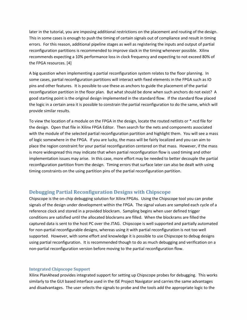
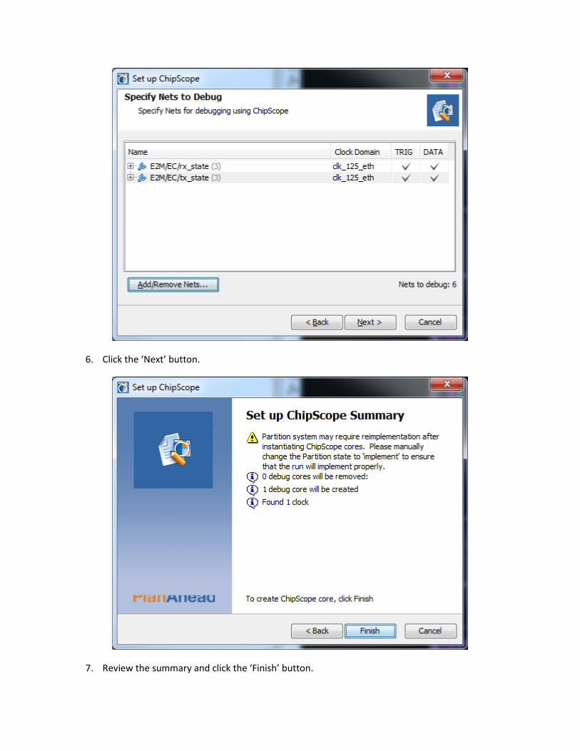
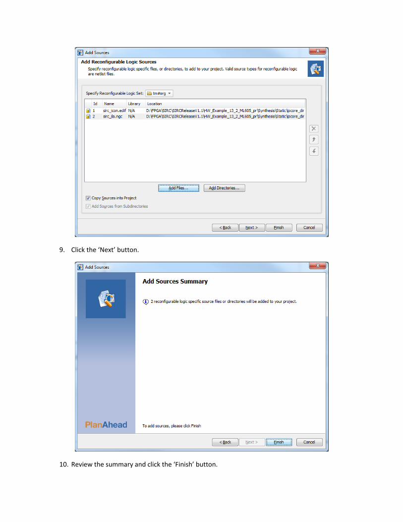
1. In the ‘Project Manager Pane’ click ‘Set up Chipscope’.
2. Here you can import a Chipscope CDC file from your debugging in the standard flow so long as it
does not contain signals of the user module in the partial reconfiguration partition. In this
example, we will proceed manually. Click the ‘Next’ button.
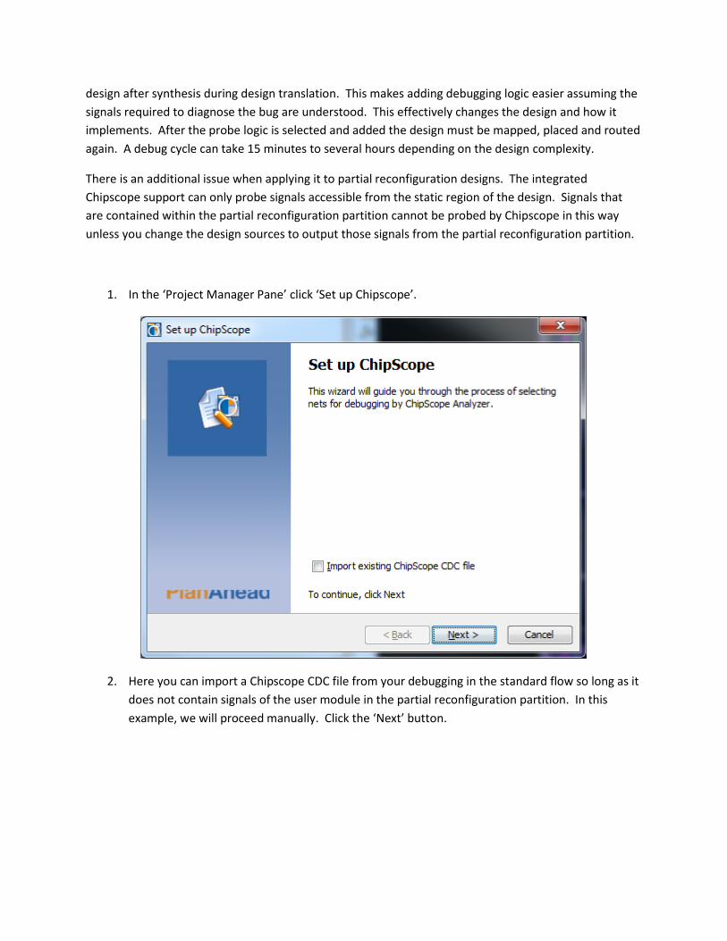
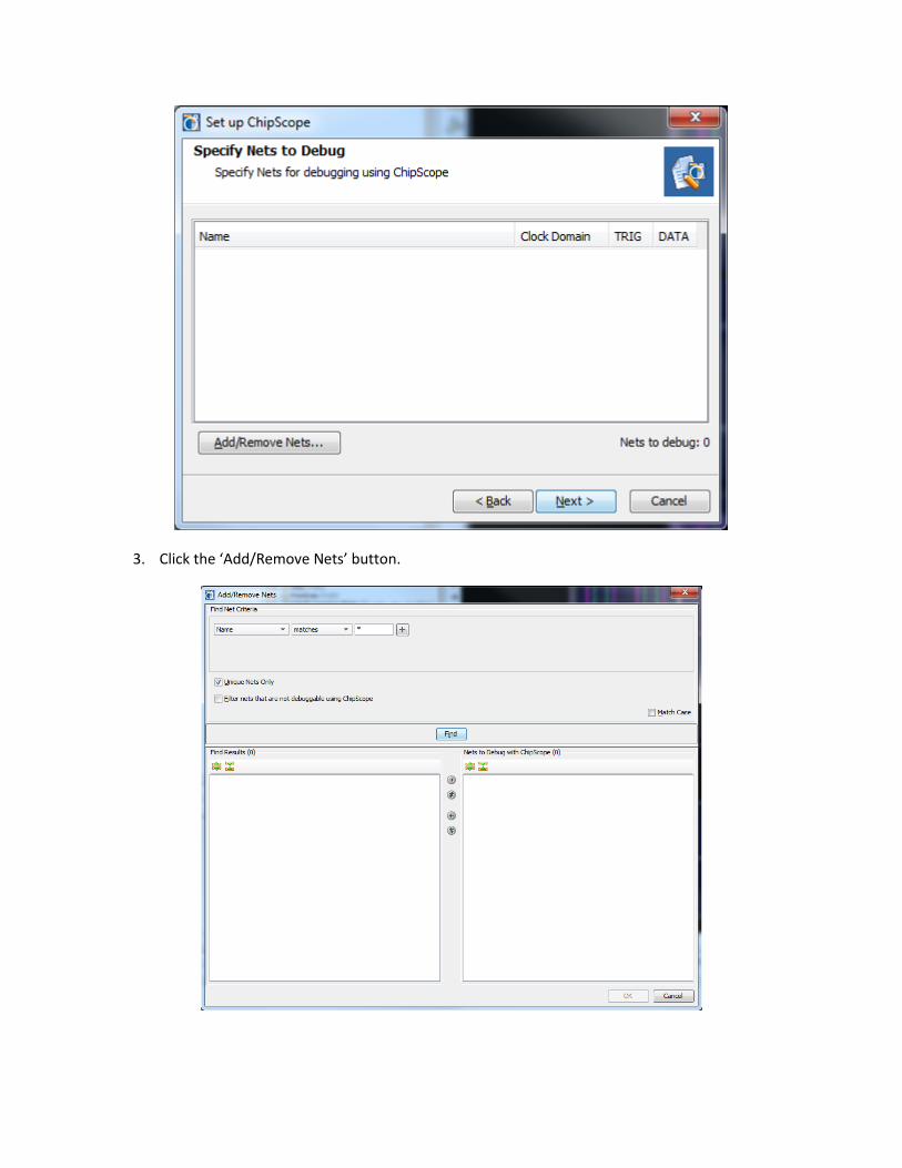
3. Click the ‘Add/Remove Nets’ button.
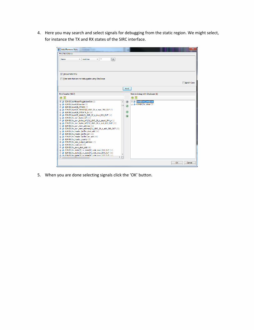
4. Here you may search and select signals for debugging from the static region. We might select,
for instance the TX and RX states of the SIRC interface.
5. When you are done selecting signals click the ‘OK’ button.
6. Click the ‘Next’ button.
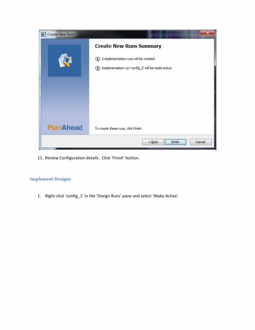
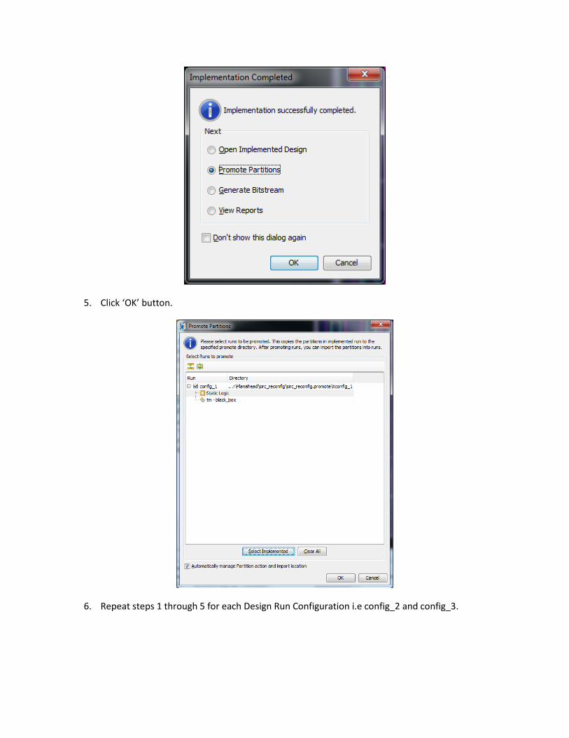
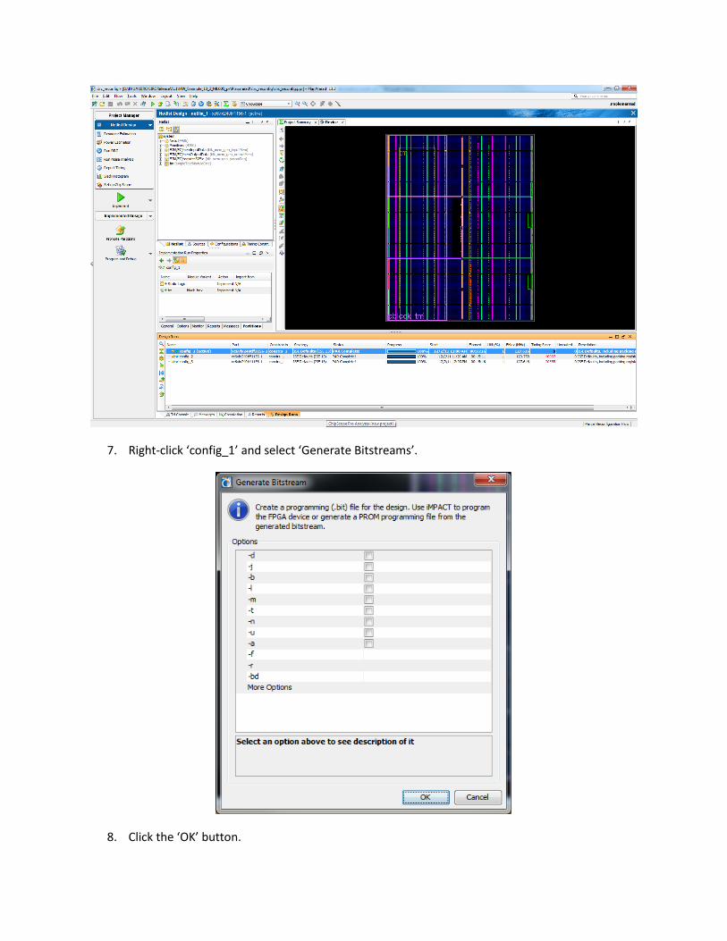
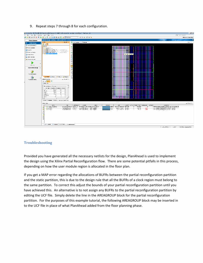
7. Review the summary and click the ‘Finish’ button.
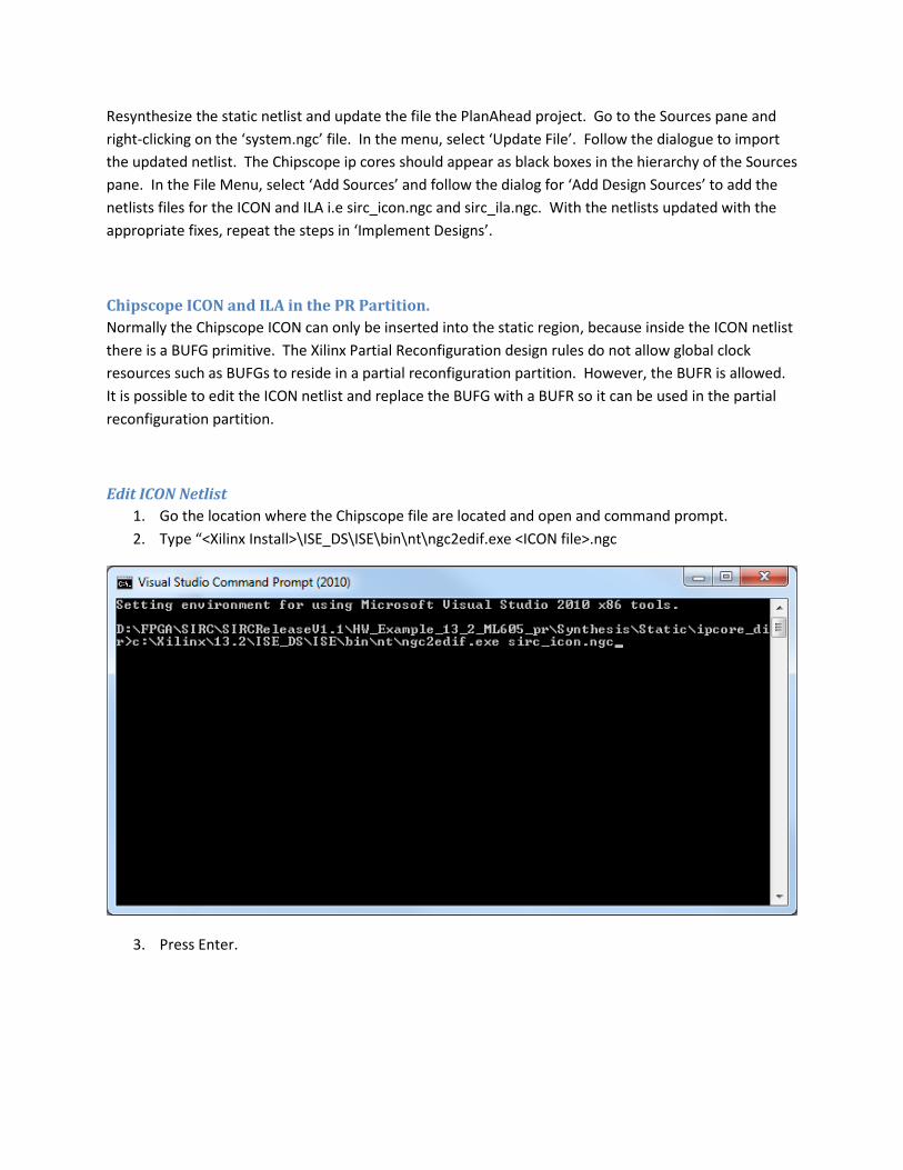
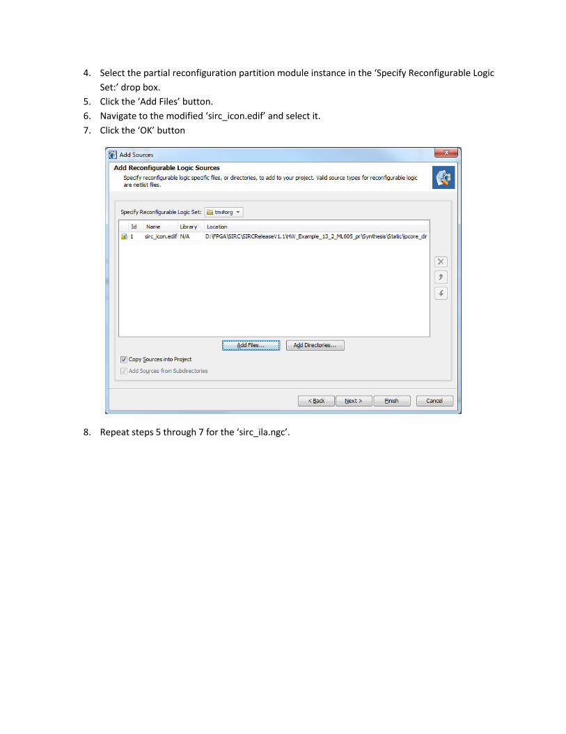
Manually Generating Chipscope IP Cores using CoreGen.[2]
The integrated Chipscope support has its advantages since it automates much of the process for
inserting the debugging infrastructure. However, it also has its limitations. It is possible to use the
debugging capabilities of Chipscope to greater efficiency by manually constructing the debugging
infrastructure in your design. The first step in this is to generate the Chipscope cores required in Xilinx
CoreGen for later instantiation in your design.
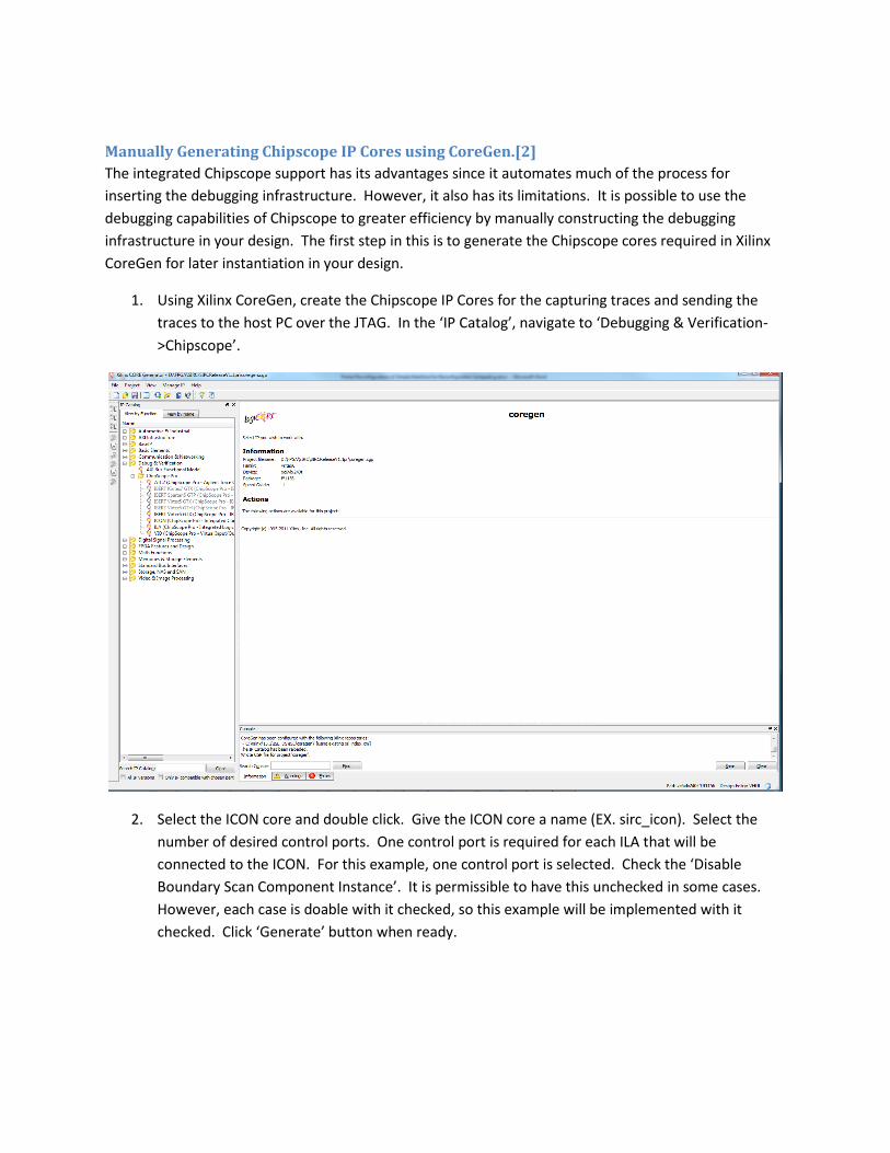
1. Using Xilinx CoreGen, create the Chipscope IP Cores for the capturing traces and sending the
traces to the host PC over the JTAG. In the ‘IP Catalog’, navigate to ‘Debugging & Verification-
>Chipscope’.
2. Select the ICON core and double click. Give the ICON core a name (EX. sirc_icon). Select the
number of desired control ports. One control port is required for each ILA that will be
connected to the ICON. For this example, one control port is selected. Check the ‘Disable
Boundary Scan Component Instance’. It is permissible to have this unchecked in some cases.
However, each case is doable with it checked, so this example will be implemented with it
checked. Click ‘Generate’ button when ready.
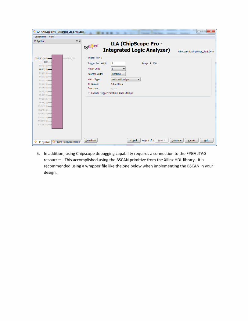
3. Select the ILA core and double click. Give the ILA core a name (EX. sirc_ila). This example is
using the default settings of the ILA. Options to note are the ‘Sample On’ and the ‘Sample Data
Depth’ parameters in ‘Storage Settings’. The ‘Sample On’ should match the desired capture
edge of the reference clock and the ‘Sample Data Depth’ to the appropriate size to for the
debug traces. The more samples the more blockram and debug logic will be required.
4. Set the ‘Trigger Port Width’ to the number of signals desired to probe using the ILA. This can be
1 to 256 signals. Click ‘Generate’ button when ready.
5. In addition, using Chipscope debugging capability requires a connection to the FPGA JTAG
resources. This accomplished using the BSCAN primitive from the Xilinx HDL library. It is
recommended using a wrapper file like the one below when implementing the BSCAN in your
design.
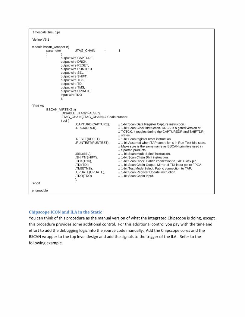
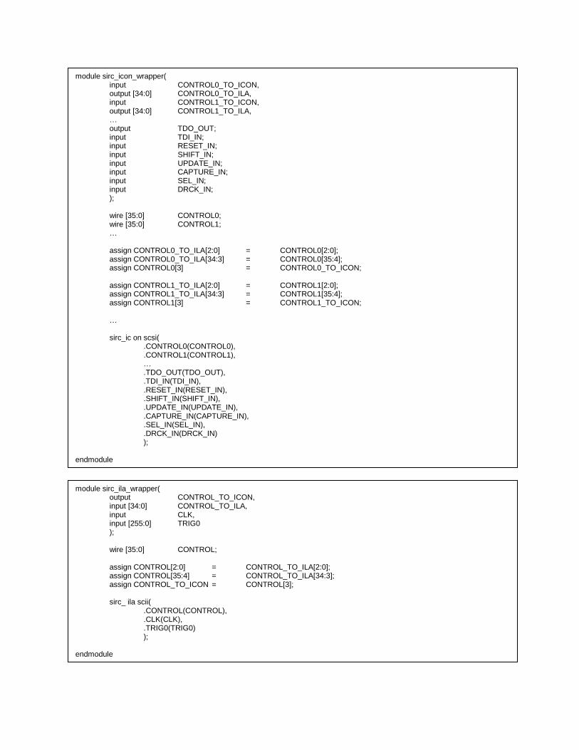
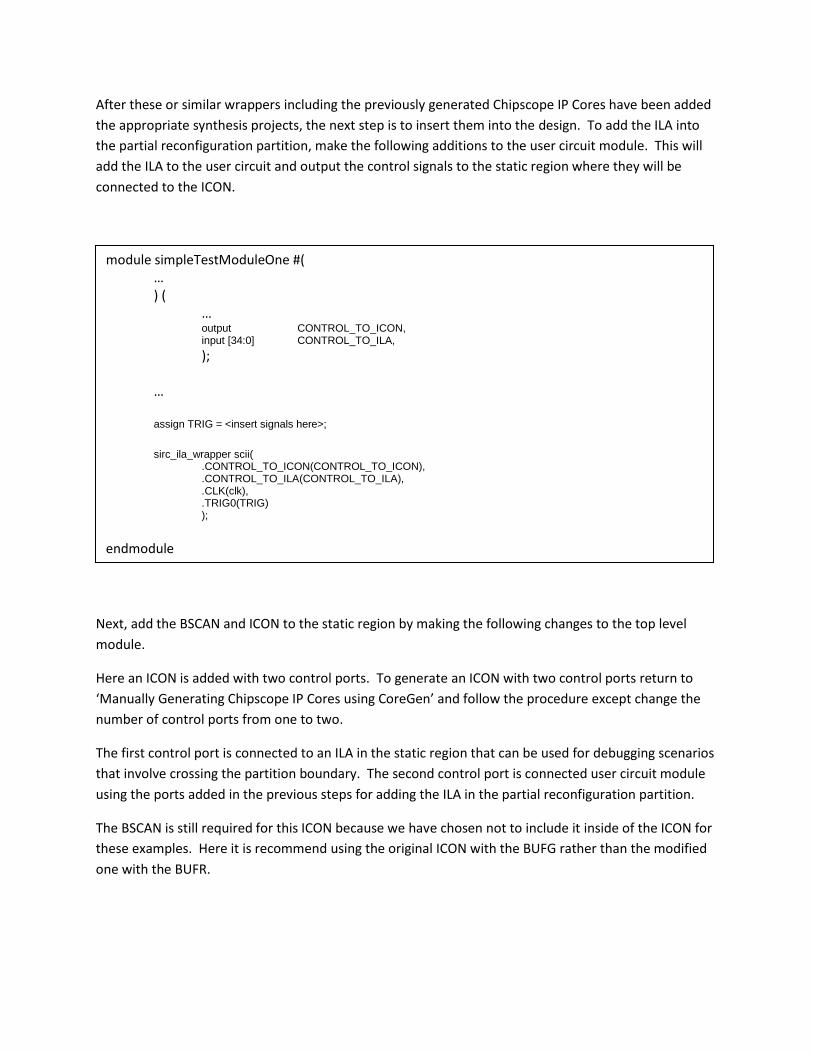
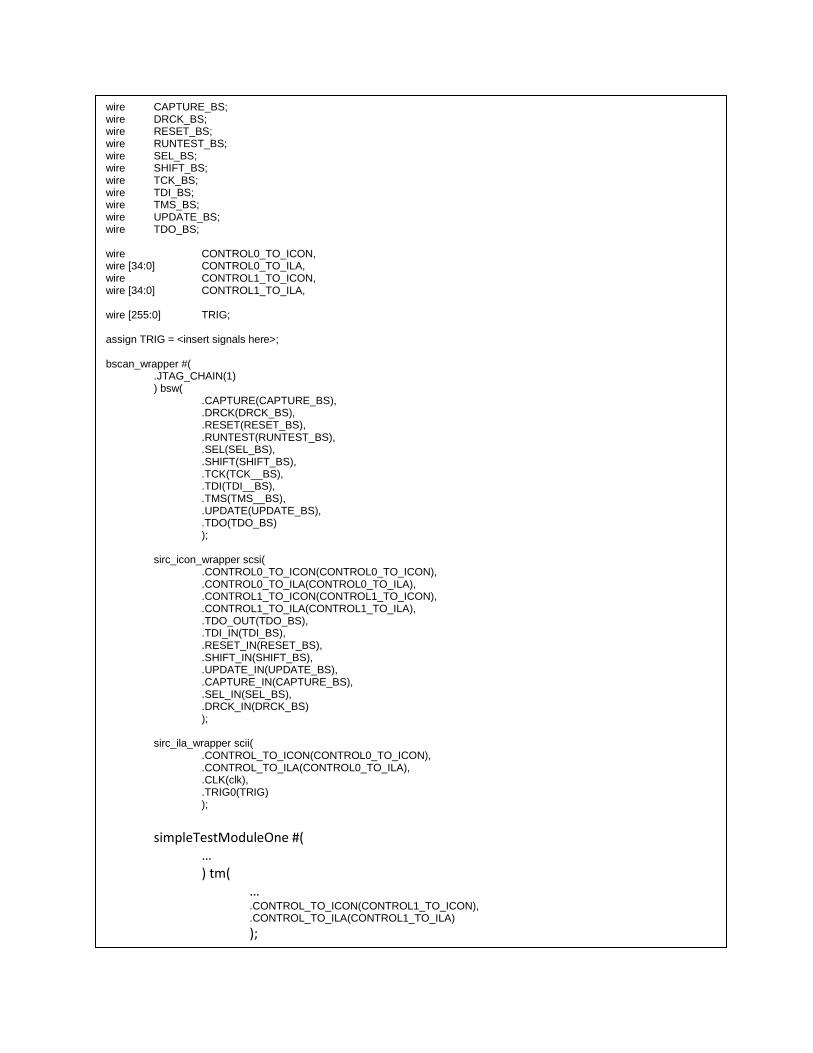
Chipscope ICON and ILA in the Static
You can think of this procedure as the manual version of what the integrated Chipscope is doing, except
this procedure provides some additional control. For this additional control you pay with the time and
effort to add the debugging logic into the source code manually. Add the Chipscope cores and the
BSCAN wrapper to the top level design and add the signals to the trigger of the ILA. Refer to the
following example.
`timescale 1ns / 1ps `define V6 1 module bscan_wrapper #( parameter JTAG_CHAIN = 1 ) ( output wire CAPTURE, output wire DRCK, output wire RESET, output wire RUNTEST, output wire SEL, output wire SHIFT, output wire TCK, output wire TDI, output wire TMS, output wire UPDATE, input wire TDO ); `ifdef V6 BSCAN_VIRTEX6 #( .DISABLE_JTAG("FALSE"), .JTAG_CHAIN(JTAG_CHAIN) // Chain number. ) bsi ( .CAPTURE(CAPTURE), // 1-bit Scan Data Register Capture instruction. .DRCK(DRCK), // 1-bit Scan Clock instruction. DRCK is a gated version of // TCTCK, it toggles during the CAPTUREDR and SHIFTDR // states. .RESET(RESET), // 1-bit Scan register reset instruction. .RUNTEST(RUNTEST), // 1-bit Asserted when TAP controller is in Run Test Idle state. // Make sure is the same name as BSCAN primitive used in // Spartan products. .SEL(SEL), // 1-bit Scan mode Select instruction. .SHIFT(SHIFT), // 1-bit Scan Chain Shift instruction. .TCK(TCK), // 1-bit Scan Clock. Fabric connection to TAP Clock pin. .TDI(TDI), // 1-bit Scan Chain Output. Mirror of TDI input pin to FPGA. .TMS(TMS), // 1-bit Test Mode Select. Fabric connection to TAP. .UPDATE(UPDATE), // 1-bit Scan Register Update instruction. .TDO(TDO) // 1-bit Scan Chain Input. ); `endif endmodule
Assign the signals to be probed to the trigger bus, TRIG. If the signals are in modules somewhere else in
the hierarchy, even partial reconfiguration partitions, they must be passed to the top static module and
assigned to the trigger bus. If the signals are part of the partial reconfiguration partition, they will cross
the partition boundary and create a new partition pin for that signal. When viewing the signals in the
Chipscope Analyzer, signals from the partial reconfiguration partition will read as high or logic 1 when
the partition is not configured or blank. This way of setting up the Chipscope debugging cores is pre
synthesis and thus does not depend on how the synthesis tools optimize signals when it comes to the