119
Advanced Design System 2011.01 - Passive Circuit DesignGuide 1 Advanced Design System 2011.01 Feburary 2011 Passive Circuit DesignGuide

Advanced Design System 2011.01 - Passive Circuit DesignGuide
1
Advanced Design System 2011.01
Feburary 2011Passive Circuit DesignGuide

Advanced Design System 2011.01 - Passive Circuit DesignGuide
2
© Agilent Technologies, Inc. 2000-20115301 Stevens Creek Blvd., Santa Clara, CA 95052 USANo part of this documentation may be reproduced in any form or by any means (includingelectronic storage and retrieval or translation into a foreign language) without prioragreement and written consent from Agilent Technologies, Inc. as governed by UnitedStates and international copyright laws.
AcknowledgmentsMentor Graphics is a trademark of Mentor Graphics Corporation in the U.S. and othercountries. Mentor products and processes are registered trademarks of Mentor GraphicsCorporation. * Calibre is a trademark of Mentor Graphics Corporation in the US and othercountries. "Microsoft®, Windows®, MS Windows®, Windows NT®, Windows 2000® andWindows Internet Explorer® are U.S. registered trademarks of Microsoft Corporation.Pentium® is a U.S. registered trademark of Intel Corporation. PostScript® and Acrobat®are trademarks of Adobe Systems Incorporated. UNIX® is a registered trademark of theOpen Group. Oracle and Java and registered trademarks of Oracle and/or its affiliates.Other names may be trademarks of their respective owners. SystemC® is a registeredtrademark of Open SystemC Initiative, Inc. in the United States and other countries and isused with permission. MATLAB® is a U.S. registered trademark of The Math Works, Inc..HiSIM2 source code, and all copyrights, trade secrets or other intellectual property rightsin and to the source code in its entirety, is owned by Hiroshima University and STARC.FLEXlm is a trademark of Globetrotter Software, Incorporated. Layout Boolean Engine byKlaas Holwerda, v1.7 http://www.xs4all.nl/~kholwerd/bool.html . FreeType Project,Copyright (c) 1996-1999 by David Turner, Robert Wilhelm, and Werner Lemberg.QuestAgent search engine (c) 2000-2002, JObjects. Motif is a trademark of the OpenSoftware Foundation. Netscape is a trademark of Netscape Communications Corporation.Netscape Portable Runtime (NSPR), Copyright (c) 1998-2003 The Mozilla Organization. Acopy of the Mozilla Public License is at http://www.mozilla.org/MPL/ . FFTW, The FastestFourier Transform in the West, Copyright (c) 1997-1999 Massachusetts Institute ofTechnology. All rights reserved.
The following third-party libraries are used by the NlogN Momentum solver:
"This program includes Metis 4.0, Copyright © 1998, Regents of the University ofMinnesota", http://www.cs.umn.edu/~metis , METIS was written by George Karypis([email protected]).
Intel@ Math Kernel Library, http://www.intel.com/software/products/mkl
SuperLU_MT version 2.0 - Copyright © 2003, The Regents of the University of California,through Lawrence Berkeley National Laboratory (subject to receipt of any requiredapprovals from U.S. Dept. of Energy). All rights reserved. SuperLU Disclaimer: THISSOFTWARE IS PROVIDED BY THE COPYRIGHT HOLDERS AND CONTRIBUTORS "AS IS"AND ANY EXPRESS OR IMPLIED WARRANTIES, INCLUDING, BUT NOT LIMITED TO, THEIMPLIED WARRANTIES OF MERCHANTABILITY AND FITNESS FOR A PARTICULAR PURPOSEARE DISCLAIMED. IN NO EVENT SHALL THE COPYRIGHT OWNER OR CONTRIBUTORS BELIABLE FOR ANY DIRECT, INDIRECT, INCIDENTAL, SPECIAL, EXEMPLARY, ORCONSEQUENTIAL DAMAGES (INCLUDING, BUT NOT LIMITED TO, PROCUREMENT OFSUBSTITUTE GOODS OR SERVICES; LOSS OF USE, DATA, OR PROFITS; OR BUSINESSINTERRUPTION) HOWEVER CAUSED AND ON ANY THEORY OF LIABILITY, WHETHER INCONTRACT, STRICT LIABILITY, OR TORT (INCLUDING NEGLIGENCE OR OTHERWISE)ARISING IN ANY WAY OUT OF THE USE OF THIS SOFTWARE, EVEN IF ADVISED OF THE
Advanced Design System 2011.01 - Passive Circuit DesignGuide
3
POSSIBILITY OF SUCH DAMAGE.
7-zip - 7-Zip Copyright: Copyright (C) 1999-2009 Igor Pavlov. Licenses for files are:7z.dll: GNU LGPL + unRAR restriction, All other files: GNU LGPL. 7-zip License: This libraryis free software; you can redistribute it and/or modify it under the terms of the GNULesser General Public License as published by the Free Software Foundation; eitherversion 2.1 of the License, or (at your option) any later version. This library is distributedin the hope that it will be useful,but WITHOUT ANY WARRANTY; without even the impliedwarranty of MERCHANTABILITY or FITNESS FOR A PARTICULAR PURPOSE. See the GNULesser General Public License for more details. You should have received a copy of theGNU Lesser General Public License along with this library; if not, write to the FreeSoftware Foundation, Inc., 59 Temple Place, Suite 330, Boston, MA 02111-1307 USA.unRAR copyright: The decompression engine for RAR archives was developed using sourcecode of unRAR program.All copyrights to original unRAR code are owned by AlexanderRoshal. unRAR License: The unRAR sources cannot be used to re-create the RARcompression algorithm, which is proprietary. Distribution of modified unRAR sources inseparate form or as a part of other software is permitted, provided that it is clearly statedin the documentation and source comments that the code may not be used to develop aRAR (WinRAR) compatible archiver. 7-zip Availability: http://www.7-zip.org/
AMD Version 2.2 - AMD Notice: The AMD code was modified. Used by permission. AMDcopyright: AMD Version 2.2, Copyright © 2007 by Timothy A. Davis, Patrick R. Amestoy,and Iain S. Duff. All Rights Reserved. AMD License: Your use or distribution of AMD or anymodified version of AMD implies that you agree to this License. This library is freesoftware; you can redistribute it and/or modify it under the terms of the GNU LesserGeneral Public License as published by the Free Software Foundation; either version 2.1 ofthe License, or (at your option) any later version. This library is distributed in the hopethat it will be useful, but WITHOUT ANY WARRANTY; without even the implied warranty ofMERCHANTABILITY or FITNESS FOR A PARTICULAR PURPOSE. See the GNU LesserGeneral Public License for more details. You should have received a copy of the GNULesser General Public License along with this library; if not, write to the Free SoftwareFoundation, Inc., 51 Franklin St, Fifth Floor, Boston, MA 02110-1301 USA Permission ishereby granted to use or copy this program under the terms of the GNU LGPL, providedthat the Copyright, this License, and the Availability of the original version is retained onall copies.User documentation of any code that uses this code or any modified version ofthis code must cite the Copyright, this License, the Availability note, and "Used bypermission." Permission to modify the code and to distribute modified code is granted,provided the Copyright, this License, and the Availability note are retained, and a noticethat the code was modified is included. AMD Availability:http://www.cise.ufl.edu/research/sparse/amd
UMFPACK 5.0.2 - UMFPACK Notice: The UMFPACK code was modified. Used by permission.UMFPACK Copyright: UMFPACK Copyright © 1995-2006 by Timothy A. Davis. All RightsReserved. UMFPACK License: Your use or distribution of UMFPACK or any modified versionof UMFPACK implies that you agree to this License. This library is free software; you canredistribute it and/or modify it under the terms of the GNU Lesser General Public Licenseas published by the Free Software Foundation; either version 2.1 of the License, or (atyour option) any later version. This library is distributed in the hope that it will be useful,but WITHOUT ANY WARRANTY; without even the implied warranty of MERCHANTABILITYor FITNESS FOR A PARTICULAR PURPOSE. See the GNU Lesser General Public License formore details. You should have received a copy of the GNU Lesser General Public Licensealong with this library; if not, write to the Free Software Foundation, Inc., 51 Franklin St,Fifth Floor, Boston, MA 02110-1301 USA Permission is hereby granted to use or copy thisprogram under the terms of the GNU LGPL, provided that the Copyright, this License, and

Advanced Design System 2011.01 - Passive Circuit DesignGuide
4
the Availability of the original version is retained on all copies. User documentation of anycode that uses this code or any modified version of this code must cite the Copyright, thisLicense, the Availability note, and "Used by permission." Permission to modify the codeand to distribute modified code is granted, provided the Copyright, this License, and theAvailability note are retained, and a notice that the code was modified is included.UMFPACK Availability: http://www.cise.ufl.edu/research/sparse/umfpack UMFPACK(including versions 2.2.1 and earlier, in FORTRAN) is available athttp://www.cise.ufl.edu/research/sparse . MA38 is available in the Harwell SubroutineLibrary. This version of UMFPACK includes a modified form of COLAMD Version 2.0,originally released on Jan. 31, 2000, also available athttp://www.cise.ufl.edu/research/sparse . COLAMD V2.0 is also incorporated as a built-infunction in MATLAB version 6.1, by The MathWorks, Inc. http://www.mathworks.com .COLAMD V1.0 appears as a column-preordering in SuperLU (SuperLU is available athttp://www.netlib.org ). UMFPACK v4.0 is a built-in routine in MATLAB 6.5. UMFPACK v4.3is a built-in routine in MATLAB 7.1.
Qt Version 4.6.3 - Qt Notice: The Qt code was modified. Used by permission. Qt copyright:Qt Version 4.6.3, Copyright (c) 2010 by Nokia Corporation. All Rights Reserved. QtLicense: Your use or distribution of Qt or any modified version of Qt implies that you agreeto this License. This library is free software; you can redistribute it and/or modify it undertheterms of the GNU Lesser General Public License as published by the Free SoftwareFoundation; either version 2.1 of the License, or (at your option) any later version. Thislibrary is distributed in the hope that it will be useful,but WITHOUT ANY WARRANTY; without even the implied warranty of MERCHANTABILITYor FITNESS FOR A PARTICULAR PURPOSE. See the GNU Lesser General Public License formore details. You should have received a copy of the GNU Lesser General Public Licensealong with this library; if not, write to the Free Software Foundation, Inc., 51 Franklin St,Fifth Floor, Boston, MA 02110-1301 USA Permission is hereby granted to use or copy thisprogram under the terms of the GNU LGPL, provided that the Copyright, this License, andthe Availability of the original version is retained on all copies.Userdocumentation of any code that uses this code or any modified version of this code mustcite the Copyright, this License, the Availability note, and "Used by permission."Permission to modify the code and to distribute modified code is granted, provided theCopyright, this License, and the Availability note are retained, and a notice that the codewas modified is included. Qt Availability: http://www.qtsoftware.com/downloads PatchesApplied to Qt can be found in the installation at:$HPEESOF_DIR/prod/licenses/thirdparty/qt/patches. You may also contact BrianBuchanan at Agilent Inc. at [email protected] for more information.
The HiSIM_HV source code, and all copyrights, trade secrets or other intellectual propertyrights in and to the source code, is owned by Hiroshima University and/or STARC.
Errata The ADS product may contain references to "HP" or "HPEESOF" such as in filenames and directory names. The business entity formerly known as "HP EEsof" is now partof Agilent Technologies and is known as "Agilent EEsof". To avoid broken functionality andto maintain backward compatibility for our customers, we did not change all the namesand labels that contain "HP" or "HPEESOF" references.
Warranty The material contained in this document is provided "as is", and is subject tobeing changed, without notice, in future editions. Further, to the maximum extentpermitted by applicable law, Agilent disclaims all warranties, either express or implied,with regard to this documentation and any information contained herein, including but notlimited to the implied warranties of merchantability and fitness for a particular purpose.

Advanced Design System 2011.01 - Passive Circuit DesignGuide
5
Agilent shall not be liable for errors or for incidental or consequential damages inconnection with the furnishing, use, or performance of this document or of anyinformation contained herein. Should Agilent and the user have a separate writtenagreement with warranty terms covering the material in this document that conflict withthese terms, the warranty terms in the separate agreement shall control.
Technology Licenses The hardware and/or software described in this document arefurnished under a license and may be used or copied only in accordance with the terms ofsuch license. Portions of this product include the SystemC software licensed under OpenSource terms, which are available for download at http://systemc.org/ . This software isredistributed by Agilent. The Contributors of the SystemC software provide this software"as is" and offer no warranty of any kind, express or implied, including without limitationwarranties or conditions or title and non-infringement, and implied warranties orconditions merchantability and fitness for a particular purpose. Contributors shall not beliable for any damages of any kind including without limitation direct, indirect, special,incidental and consequential damages, such as lost profits. Any provisions that differ fromthis disclaimer are offered by Agilent only.
Restricted Rights Legend U.S. Government Restricted Rights. Software and technicaldata rights granted to the federal government include only those rights customarilyprovided to end user customers. Agilent provides this customary commercial license inSoftware and technical data pursuant to FAR 12.211 (Technical Data) and 12.212(Computer Software) and, for the Department of Defense, DFARS 252.227-7015(Technical Data - Commercial Items) and DFARS 227.7202-3 (Rights in CommercialComputer Software or Computer Software Documentation).
Advanced Design System 2011.01 - Passive Circuit DesignGuide
6
About Passive Circuit DesignGuide . . . . . . . . . . . . . . . . . . . . . . . . . . . . . . . . . . . . . . . . . . . . 8 Step-by-Step Example . . . . . . . . . . . . . . . . . . . . . . . . . . . . . . . . . . . . . . . . . . . . . . . . . . . 8 Setting Up the Design Environment . . . . . . . . . . . . . . . . . . . . . . . . . . . . . . . . . . . . . . . . . . 8 Designing and Analyzing a Network . . . . . . . . . . . . . . . . . . . . . . . . . . . . . . . . . . . . . . . . . . 12
Using SmartComponents in Passive Circuit DesignGuide . . . . . . . . . . . . . . . . . . . . . . . . . . . . . 18 Placing and Editing SmartComponents . . . . . . . . . . . . . . . . . . . . . . . . . . . . . . . . . . . . . . . . 18 Copying SmartComponents . . . . . . . . . . . . . . . . . . . . . . . . . . . . . . . . . . . . . . . . . . . . . . . 20 Deleting SmartComponents . . . . . . . . . . . . . . . . . . . . . . . . . . . . . . . . . . . . . . . . . . . . . . . 20 Using SmartComponents as Standalone Components . . . . . . . . . . . . . . . . . . . . . . . . . . . . . 21
Using Automated Assistants in Passive Circuit DesignGuide . . . . . . . . . . . . . . . . . . . . . . . . . . . 23 Automated Design and Analysis . . . . . . . . . . . . . . . . . . . . . . . . . . . . . . . . . . . . . . . . . . . . 23 Design Assistant . . . . . . . . . . . . . . . . . . . . . . . . . . . . . . . . . . . . . . . . . . . . . . . . . . . . . . . 24 Simulation Assistant . . . . . . . . . . . . . . . . . . . . . . . . . . . . . . . . . . . . . . . . . . . . . . . . . . . . 24 Optimization Assistant . . . . . . . . . . . . . . . . . . . . . . . . . . . . . . . . . . . . . . . . . . . . . . . . . . . 26 Display Assistant . . . . . . . . . . . . . . . . . . . . . . . . . . . . . . . . . . . . . . . . . . . . . . . . . . . . . . . 27 Layout Generation . . . . . . . . . . . . . . . . . . . . . . . . . . . . . . . . . . . . . . . . . . . . . . . . . . . . . . 31 Passive RLC Components . . . . . . . . . . . . . . . . . . . . . . . . . . . . . . . . . . . . . . . . . . . . . . . . . 31 MICapP (Microstrip 4-port Interdigital Capacitor) . . . . . . . . . . . . . . . . . . . . . . . . . . . . . . . . 32 MICapPG (Microstrip Grounded 2-port Interdigital Capacitor) . . . . . . . . . . . . . . . . . . . . . . . . 33 MICapS (Microstrip 2-port Interdigital Capacitor) . . . . . . . . . . . . . . . . . . . . . . . . . . . . . . . . 34 MICapSG (Microstrip 1-port Interdigital Capacitor) . . . . . . . . . . . . . . . . . . . . . . . . . . . . . . . 36 MREInd (Microstrip Elevated Rectangular Inductor) . . . . . . . . . . . . . . . . . . . . . . . . . . . . . . . 37 MRInd (Microstrip Rectangular Inductor) SmartComponent . . . . . . . . . . . . . . . . . . . . . . . . . 39 MSInd (Microstrip Spiral Inductor) . . . . . . . . . . . . . . . . . . . . . . . . . . . . . . . . . . . . . . . . . . . 41 MTFC (Microstrip Thin Film Capacitor) SmartComponent . . . . . . . . . . . . . . . . . . . . . . . . . . . 42 TFC (Thin Film Capacitor) SmartComponent . . . . . . . . . . . . . . . . . . . . . . . . . . . . . . . . . . . . 43 TFR (Thin Film Resistor) SmartComponent . . . . . . . . . . . . . . . . . . . . . . . . . . . . . . . . . . . . . 44 Passive Microstrip Components . . . . . . . . . . . . . . . . . . . . . . . . . . . . . . . . . . . . . . . . . . . . . 46 MBend (Microstrip Bend Component) . . . . . . . . . . . . . . . . . . . . . . . . . . . . . . . . . . . . . . . . . 46 MBStub (Microstrip Butterfly Radial Stub) . . . . . . . . . . . . . . . . . . . . . . . . . . . . . . . . . . . . . . 47 MCFil (Microstrip Coupled-Line Filter Element) . . . . . . . . . . . . . . . . . . . . . . . . . . . . . . . . . . 48 MCLine (Microstrip Coupled Line Component) . . . . . . . . . . . . . . . . . . . . . . . . . . . . . . . . . . . 49 MCorn (Microstrip Corner Component) . . . . . . . . . . . . . . . . . . . . . . . . . . . . . . . . . . . . . . . . 49 MCross (Microstrip Cross Component) . . . . . . . . . . . . . . . . . . . . . . . . . . . . . . . . . . . . . . . . 50 MCurve (Microstrip Curve Component) . . . . . . . . . . . . . . . . . . . . . . . . . . . . . . . . . . . . . . . . 50 MGap (Microstrip Gap Component) . . . . . . . . . . . . . . . . . . . . . . . . . . . . . . . . . . . . . . . . . . 51 MLine (Microstrip Line) . . . . . . . . . . . . . . . . . . . . . . . . . . . . . . . . . . . . . . . . . . . . . . . . . . . 52 MMndr (Microstrip Meander Line) . . . . . . . . . . . . . . . . . . . . . . . . . . . . . . . . . . . . . . . . . . . 52 MRStub (Microstrip Radial Stub) SmartComponent . . . . . . . . . . . . . . . . . . . . . . . . . . . . . . . 53 MStep (Microstrip Step Component) . . . . . . . . . . . . . . . . . . . . . . . . . . . . . . . . . . . . . . . . . 54 MStub (Microstrip Stub) . . . . . . . . . . . . . . . . . . . . . . . . . . . . . . . . . . . . . . . . . . . . . . . . . . 55 MTaper (Microstrip Taper Component) . . . . . . . . . . . . . . . . . . . . . . . . . . . . . . . . . . . . . . . . 56 MTee (Microstrip Tee Component) . . . . . . . . . . . . . . . . . . . . . . . . . . . . . . . . . . . . . . . . . . . 56 Passive Microstrip Circuits . . . . . . . . . . . . . . . . . . . . . . . . . . . . . . . . . . . . . . . . . . . . . . . . 57 BLCoupler (Branch-Line Coupler) . . . . . . . . . . . . . . . . . . . . . . . . . . . . . . . . . . . . . . . . . . . 57 CLCoupler (Coupled-Line Coupler) . . . . . . . . . . . . . . . . . . . . . . . . . . . . . . . . . . . . . . . . . . . 59 CLFilter (Coupled-Line Filter) . . . . . . . . . . . . . . . . . . . . . . . . . . . . . . . . . . . . . . . . . . . . . . 60 CMFilter (Comb-Line Filter) . . . . . . . . . . . . . . . . . . . . . . . . . . . . . . . . . . . . . . . . . . . . . . . . 61 DSMatch (Double-Stub Match) . . . . . . . . . . . . . . . . . . . . . . . . . . . . . . . . . . . . . . . . . . . . . 63 HPFilter (Hairpin Filter) . . . . . . . . . . . . . . . . . . . . . . . . . . . . . . . . . . . . . . . . . . . . . . . . . . 64 IDFilter (Interdigital Filter) . . . . . . . . . . . . . . . . . . . . . . . . . . . . . . . . . . . . . . . . . . . . . . . . 66 LCoupler (Lange Coupler) . . . . . . . . . . . . . . . . . . . . . . . . . . . . . . . . . . . . . . . . . . . . . . . . . 67 LEMatch (Lumped Component Match) . . . . . . . . . . . . . . . . . . . . . . . . . . . . . . . . . . . . . . . . 68 QWMatch (Quarter-Wave Match) . . . . . . . . . . . . . . . . . . . . . . . . . . . . . . . . . . . . . . . . . . . . 70

Advanced Design System 2011.01 - Passive Circuit DesignGuide
7
RAtten (Resistive Attenuator) . . . . . . . . . . . . . . . . . . . . . . . . . . . . . . . . . . . . . . . . . . . . . . 71 RRCoupler (Rat-Race Coupler) . . . . . . . . . . . . . . . . . . . . . . . . . . . . . . . . . . . . . . . . . . . . . 72 SBFilter (Stub Bandpass Filter) . . . . . . . . . . . . . . . . . . . . . . . . . . . . . . . . . . . . . . . . . . . . . 73 SIFilter (Stepped Impedance Lowpass Filter) . . . . . . . . . . . . . . . . . . . . . . . . . . . . . . . . . . . 75 SLFilter (Stub Lowpass Filter) . . . . . . . . . . . . . . . . . . . . . . . . . . . . . . . . . . . . . . . . . . . . . . 76 SRFilter (Stepped Impedance Resonator Filter) . . . . . . . . . . . . . . . . . . . . . . . . . . . . . . . . . . 78 SSMatch (Single-Stub Match) . . . . . . . . . . . . . . . . . . . . . . . . . . . . . . . . . . . . . . . . . . . . . . 79 TCoupler (Tee Power Divider) . . . . . . . . . . . . . . . . . . . . . . . . . . . . . . . . . . . . . . . . . . . . . . 81 TLMatch (Tapered-Line Match) . . . . . . . . . . . . . . . . . . . . . . . . . . . . . . . . . . . . . . . . . . . . . 82 WDCoupler (Wilkinson Divider) . . . . . . . . . . . . . . . . . . . . . . . . . . . . . . . . . . . . . . . . . . . . . 83 ZZFilter (Zig-Zag Coupled-Line Filter) . . . . . . . . . . . . . . . . . . . . . . . . . . . . . . . . . . . . . . . . 85 Passive Stripline Components . . . . . . . . . . . . . . . . . . . . . . . . . . . . . . . . . . . . . . . . . . . . . . 86 SBend (Stripline Bend Component) . . . . . . . . . . . . . . . . . . . . . . . . . . . . . . . . . . . . . . . . . . 86 SCLine (Stripline Coupled Line Component) . . . . . . . . . . . . . . . . . . . . . . . . . . . . . . . . . . . . 87 SCross (Stripline Cross Component) . . . . . . . . . . . . . . . . . . . . . . . . . . . . . . . . . . . . . . . . . 88 SCurve (Stripline Curve Component) . . . . . . . . . . . . . . . . . . . . . . . . . . . . . . . . . . . . . . . . . 89 SLine (Stripline Line Component) . . . . . . . . . . . . . . . . . . . . . . . . . . . . . . . . . . . . . . . . . . . 89 SStep (Stripline Step Component) . . . . . . . . . . . . . . . . . . . . . . . . . . . . . . . . . . . . . . . . . . . 90 SStub (Stripline Stub Component) . . . . . . . . . . . . . . . . . . . . . . . . . . . . . . . . . . . . . . . . . . . 90 STee (Stripline Tee Component) . . . . . . . . . . . . . . . . . . . . . . . . . . . . . . . . . . . . . . . . . . . . 91 Passive Stripline Circuits . . . . . . . . . . . . . . . . . . . . . . . . . . . . . . . . . . . . . . . . . . . . . . . . . 92 . . . . . . . . . . . . . . . . . . . . . . . . . . . . . . . . . . . . . . . . . . . . . . . . . . . . . . . . . . . . . . . . . . . 92 SBLCoupler (Stripline Branch-Line Coupler) . . . . . . . . . . . . . . . . . . . . . . . . . . . . . . . . . . . . 92 SCLCoupler (Stripline Coupled-Line Coupler) . . . . . . . . . . . . . . . . . . . . . . . . . . . . . . . . . . . 94 SCLFilter (Stripline Coupled-Line Filter) . . . . . . . . . . . . . . . . . . . . . . . . . . . . . . . . . . . . . . . 95 SCMFilter (Stripline Comb-Line Filter) . . . . . . . . . . . . . . . . . . . . . . . . . . . . . . . . . . . . . . . . 97 SDSMatch (Stripline Double-Stub Match) . . . . . . . . . . . . . . . . . . . . . . . . . . . . . . . . . . . . . . 99 SHPFilter (Stripline Hairpin Filter) . . . . . . . . . . . . . . . . . . . . . . . . . . . . . . . . . . . . . . . . . . . 100 SIDFilter (Stripline Interdigital Filter) . . . . . . . . . . . . . . . . . . . . . . . . . . . . . . . . . . . . . . . . . 102 SQWMatch (Stripline Quarter-Wave Match) . . . . . . . . . . . . . . . . . . . . . . . . . . . . . . . . . . . . 104 SRRCoupler (Stripline Rat-Race Coupler) . . . . . . . . . . . . . . . . . . . . . . . . . . . . . . . . . . . . . . 106 SSBFilter (Stripline Stub Bandpass Filter) . . . . . . . . . . . . . . . . . . . . . . . . . . . . . . . . . . . . . . 107 SSIFilter (Stripline Stepped Impedance Lowpass Filter) . . . . . . . . . . . . . . . . . . . . . . . . . . . . 109 SSLFilter (Stripline Stub Lowpass Filter) . . . . . . . . . . . . . . . . . . . . . . . . . . . . . . . . . . . . . . . 111 SSRFilter (Stripline Stepped Impedance Resonator Filter) . . . . . . . . . . . . . . . . . . . . . . . . . . 113 SSSMatch (Stripline Single-Stub Match) . . . . . . . . . . . . . . . . . . . . . . . . . . . . . . . . . . . . . . . 115 STCoupler (Stripline Tee Power Divider) . . . . . . . . . . . . . . . . . . . . . . . . . . . . . . . . . . . . . . . 117 SWDCoupler (Stripline Wilkinson Divider) . . . . . . . . . . . . . . . . . . . . . . . . . . . . . . . . . . . . . . 118

Advanced Design System 2011.01 - Passive Circuit DesignGuide
8
About Passive Circuit DesignGuideThe Passive Circuit DesignGuide documentation provides an introduction to the PassiveCircuit DesignGuide. The complexity of the Advanced Design System (ADS) is made easilyaccessible through the automated capability. A first-time or casual ADS user can beginusing the capability of ADS quickly, while experienced ADS users can perform tasks fasterthan ever before. The Step-by-Step Example describes how a microstrip line and acoupled-line filter can be designed and verified, and a layout generated, in a few minutes.
The Passive Circuit DesignGuide provides SmartComponents and automated-assistants forthe design and simulation. All SmartComponents can be modified. You simply select aSmartComponent and, with little effort, redesign or verify their performance. The UsingSmartComponents (dgpas) section answers many common questions relating toDesignGuide use. The section Using Automated Assistants (dgpas) introduces AutomatedAssistants.
Step-by-Step ExampleThe step-by-step example takes you through the design, analysis and sensitivitysimulation of a microstrip line and a coupled-line filter. After completing this example, youshould have a basic understanding of the Utility and be ready to begin using the tool.Follow these steps to begin:
Setting Up the Design Environment
Designing and Analyzing a Network
NoteYou should already be familiar with the basic features of Advanced Design System. For help withADS basic features, refer to the Schematic Capture and Layout (usrguide) documentation.
Setting Up the Design EnvironmentBefore you can use the Passive Circuit DesignGuide, you must set up the designenvironment by using these steps:
Setting DesignGuide Preferences
Opening a Workspace
Opening a Schematic Window
Opening the Passive Circuit DesignGuide
Displaying the SmartComponent Palette
NoteBefore beginning, you must have installed the DesignGuide with appropriate licensing codewords.
Setting DesignGuide Preferences
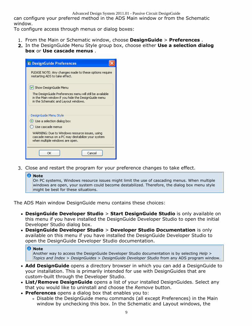
All DesignGuides can be accessed through either cascading menus or dialog boxes. You
Advanced Design System 2011.01 - Passive Circuit DesignGuide
9
can configure your preferred method in the ADS Main window or from the Schematicwindow.To configure access through menus or dialog boxes:
From the Main or Schematic window, choose DesignGuide > Preferences .1.In the DesignGuide Menu Style group box, choose either Use a selection dialog2.box or Use cascade menus .
Close and restart the program for your preference changes to take effect.3.
NoteOn PC systems, Windows resource issues might limit the use of cascading menus. When multiplewindows are open, your system could become destabilized. Therefore, the dialog box menu stylemight be best for these situations.
The ADS Main window DesignGuide menu contains these choices:
DesignGuide Developer Studio > Start DesignGuide Studio is only available onthis menu if you have installed the DesignGuide Developer Studio to open the initialDeveloper Studio dialog box.DesignGuide Developer Studio > Developer Studio Documentation is onlyavailable on this menu if you have installed the DesignGuide Developer Studio toopen the DesignGuide Developer Studio documentation.
NoteAnother way to access the DesignGuide Developer Studio documentation is by selecting Help >Topics and Index > DesignGuides > DesignGuide Developer Studio from any ADS program window.
Add DesignGuide opens a directory browser in which you can add a DesignGuide toyour installation. This is primarily intended for use with DesignGuides that arecustom-built through the Developer Studio.List/Remove DesignGuide opens a list of your installed DesignGuides. Select anythat you would like to uninstall and choose the Remove button.Preferences opens a dialog box that enables you to:
Disable the DesignGuide menu commands (all except Preferences) in the Mainwindow by unchecking this box. In the Schematic and Layout windows, the
Advanced Design System 2011.01 - Passive Circuit DesignGuide
10
complete DesignGuide menu and all of its commands are removed if this box isunchecked.Select your preferred interface method, either cascading menus or dialog boxes.
Opening a Workspace
The ADS design environment is set up within a Workspace.
To create a new Workspace:
From the ADS Main window, choose File > New > Workspace or click Create a1.New Workspace on the toolbar.
In the dialog, define the location of the Workspace and assign a Workspace name.2.
For more details on creating a new space, refer to Using Workspace (adstour).
Opening a Schematic Window
A new schematic is needed to contain the lowpass component for this example.
To open a Schematic window:
From the ADS Main window, choose Window > New Schematic or click New1.Schematic Window on the toolbar. A new Schematic window appears.
NoteDepending on how your ADS preferences are set, a Schematic window can appear automaticallywhen you create or open a Workspace.
In the New Schematic window, provide Library and Cell details to create a cell named2.Example .
For more details on creating a new schematic, refer Using Designs (adstour).
Opening the Passive Circuit DesignGuide
The Passive Circuit DesignGuide is accessed from the DesignGuide menu in theSchematic window.
To open the Passive Circuit DesignGuide:

Advanced Design System 2011.01 - Passive Circuit DesignGuide
11
In the Schematic window, choose DesignGuide > Passive Circuit > Passive1.Circuit Control Window. The Control window opens.
Using the Control Window
All Utility features are available from the Control window. The Control window housesmenus, a toolbar, and SmartComponent manipulation controls. The menus and toolbarbuttons perform the basic functions of design, delete, and display the SmartComponentpalette. Full features are available from each of the tab pages on the window. The windowcan be placed anywhere on the screen. Explore each tab page by clicking on the tab at thetop of each page. Explore the window menus as well to familiarize yourself with the basicUtility capabilities.
The pull-down lists at the top of the control window are designed to help you navigatemultiple schematic windows and SmartComponents. You can use the Current Schematicdrop-down list box to select any of the currently opened schematic windows. This field isupdated any time the Passive Circuit Control Window is selected from the Tools menu.From the SmartComponent drop-down list box, you can select any of theSmartComponents on the currently selected schematic window.

Advanced Design System 2011.01 - Passive Circuit DesignGuide
12
To close the Control window:
Select File > Exit DesignGuide from the Control window menubar. (You can alsoclose the window by clicking the x at the top of the window.)
Continue the step-by-step example by Designing and Analyzing a Network.
Designing and Analyzing a NetworkIn this step-by-step example, you design a microstrip line, and complete the design,analysis, and optimization of a branch-line coupler. A microstrip line can be designedeasily given a substrate definition, its characteristic impedance, and length. Using theUtility follows a normal design flow procedure:
Select components needed for your design from the component palettes (Displayingthe SmartComponent Palette) and place the component in your design (PlacingComponents in the Design).
Provide specifications (Changing Component Parameters).
Design and analyze the component (Designing the SmartComponent and Optimizingthe Branch-Line Coupler).
NoteBefore starting this section of the step-by-step example, confirm your setup (Setting Up the DesignEnvironment).
Displaying the SmartComponent Palette
The DesignGuide contains six SmartComponent palettes that provide quick and easyaccess to the SmartComponents. The six available component palettes are:
All contains all of the SmartComponents.Lines contains the simple line element SmartComponents.RLC contains the distributed resistor, inductor, and capacitor SmartComponents.Couplers contains the coupler and power divider SmartComponents.Filters contains the distributed filter SmartComponents.Match contains the distributed and lumped matching SmartComponents.A blue accent in the upper-left corner of a palette button indicates the component isa SmartComponent.

Advanced Design System 2011.01 - Passive Circuit DesignGuide
13
You can display the SmartComponent palettes in one of these ways:
By clicking Component Palette on the Control window toolbarBy choosing View > Component Palette from the Control window menuBy selecting the palette from the Component Palette drop-down list box in theSchematic window toolbar (directly above the palette).
Placing Components in the Design
To place a component in the design:
Display the Passive Circuit - Microstrip palette.1.Click MSUB on the component palette to select the component.2.
Click within the schematic window to place the component.3.
You can change the orientation of the SmartComponent before placement byselecting from the Insert > Component > Component Orientationcommands or by selecting Rotate by -90 repeatedly from the schematictoolbar.The place component mode remains active until you choose Edit > EndCommand from the schematic toolbar.

Advanced Design System 2011.01 - Passive Circuit DesignGuide
14
NoteWhen a SmartComponent is placed initially, a temporary component is used to place andspecify the parameters for the SmartComponent. This component does not contain asubnetwork design. After the DesignGuide has been used to design the SmartComponent, thetemporary component is replaced with a permanent component. The SmartComponent isrenamed to DA_ComponentName_DesignName and an autogenerated design is placed insidethe SmartComponent's subnetwork design file. Subsequently, if the SmartComponentparameters are edited, the DesignGuide must be used again to update the subnetwork designfile.
Changing Component Parameters
To edit the component parameters:
In the Schematic window, double-click the MSUB component to open the component1.parameter dialog box.Change the substrate thickness (H) to 20 mil and the dielectric constant (Er)2.to 5 .
NoteSee Placing and Editing SmartComponents (dgpas) for details on changing parameters in the designwindow or component dialog box.
To place the SmartComponent in the design:
Click MLine on the component palette to select the component.1.
Click within the schematic window to place the component.2.
To edit the component parameters:
In the Schematic window, double-click the MLine component to open the component1.parameter dialog.Change the center frequency (F) to 5 GHz , the characteristic impedance (Zo)2.to 75 Ohm , and the electrical length (Lelec) to 0.25 wavelengths .
Designing the SmartComponent
You can design and analyze the SmartComponent from the Control Window.
To start the simulation:
Select DA_MLine1 from the SmartComponent drop-down list.1.On the Design Assistant tab, click Design to start a simulation and generate the2.design for the SmartComponent.
Examining the SmartComponent Design

Advanced Design System 2011.01 - Passive Circuit DesignGuide
15
You can look at the details of the autogenerated design inside the SmartComponent'ssubnetwork.
To examine the component's subnetwork:
Select the component DA_MLine1.1.Click Push Into Hierarchy on the schematic toolbar.2.After examining the design, click Pop Out on the schematic toolbar to close the view.3.
Deleting the SmartComponent
To delete the DA_MLine1 SmartComponent, choose Tools > DeleteSmartComponent from the Control window. Do not delete the MSUB component .
NoteThe Delete button on the Control window is different from the Delete button on the ADS schematicwindow toolbar.
Designing and Analyzing a Branch-Line Coupler
A branch-line coupler can be designed as easily as a microstrip line.
To design and analyze a branch-line coupler:
In the Passive Circuit - Microstrip palette, select BLCplr and place the component in1.the Schematic window.Click the BLCoupler component and change the center frequency (F) to 5 GHz.2.Choose the BLCoupler component in the SmartComponent drop-down list box on3.the Control Window and then click the Design Assistant tab.Click Design to generate the design for the SmartComponent.4.Click the Simulation Assistant tab on the Control Window and enter 1 GHz start5.frequency, 10 GHz stop, 20 MHz step (accept default display specifications).Click Simulate to analyze the SmartComponent. The analysis results are shown6.here.
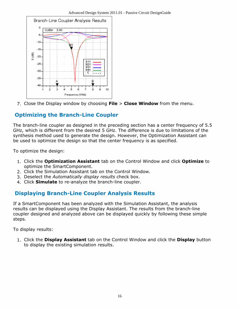
Advanced Design System 2011.01 - Passive Circuit DesignGuide
16
Close the Display window by choosing File > Close Window from the menu.7.
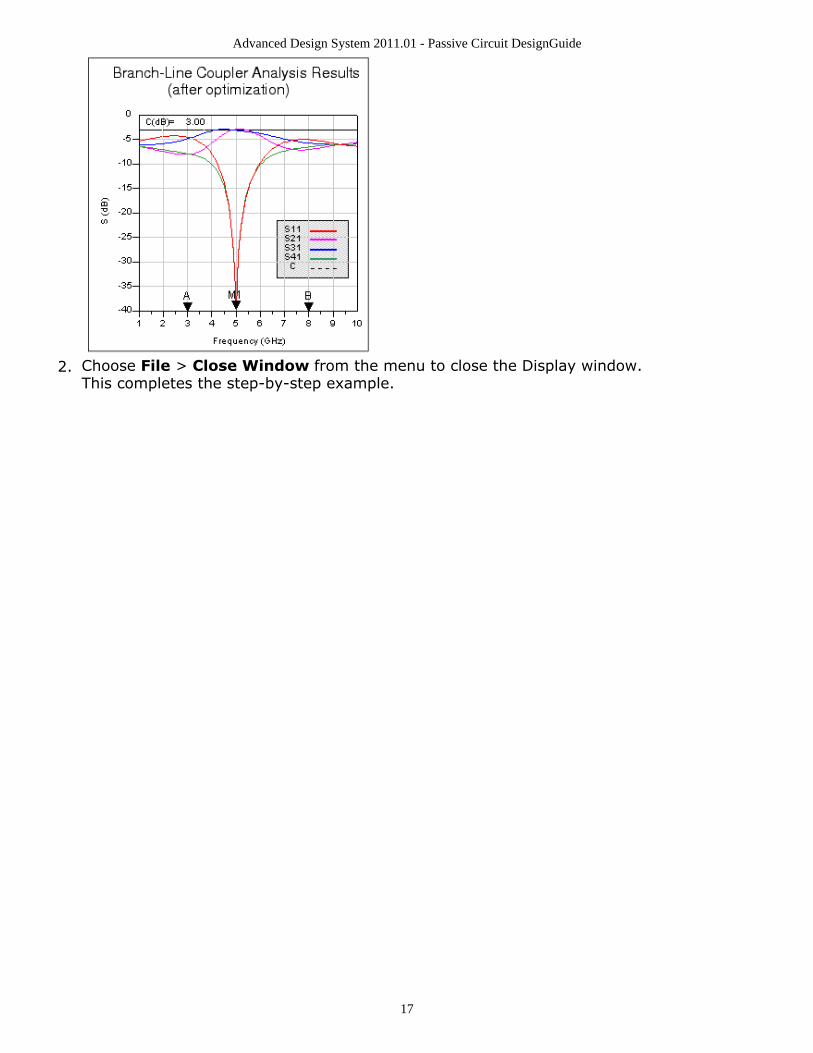
Optimizing the Branch-Line Coupler
The branch-line coupler as designed in the preceding section has a center frequency of 5.5GHz, which is different from the desired 5 GHz. The difference is due to limitations of thesynthesis method used to generate the design. However, the Optimization Assistant canbe used to optimize the design so that the center frequency is as specified.
To optimize the design:
Click the Optimization Assistant tab on the Control Window and click Optimize to1.optimize the SmartComponent.Click the Simulation Assistant tab on the Control Window.2.Deselect the Automatically display results check box.3.Click Simulate to re-analyze the branch-line coupler.4.
Displaying Branch-Line Coupler Analysis Results
If a SmartComponent has been analyzed with the Simulation Assistant, the analysisresults can be displayed using the Display Assistant. The results from the branch-linecoupler designed and analyzed above can be displayed quickly by following these simplesteps.
To display results:
Click the Display Assistant tab on the Control Window and click the Display button1.to display the existing simulation results.
Advanced Design System 2011.01 - Passive Circuit DesignGuide
17
Choose File > Close Window from the menu to close the Display window.2.This completes the step-by-step example.
Advanced Design System 2011.01 - Passive Circuit DesignGuide
18
Using SmartComponents in PassiveCircuit DesignGuideThis DesignGuide provides a large number of passive SmartComponents such as couplers,filters, lines and matching networks. SmartComponents are smart sub-network designsthat provide the container for specification parameters and a schematic representation ofthe design when placed into a design. The DesignGuide provides automated design andanalysis for these SmartComponents.
Placing and Editing SmartComponentsSmartComponents can be placed, copied, edited and deleted like other components in theAdvanced Design System. The basics of placement, copying, editing and deleting aredescribed briefly in this section.
NoteFor help with ADS basic features, refer to the Schematic Capture and Layout (usrguide) documentation.
The DesignGuide contains six SmartComponent palettes that provide quick and easyaccess to the SmartComponents. The six available component palettes are:
All contains all of the SmartComponents.Lines contains the simple line element SmartComponents.RLC contains the distributed resistor, inductor, and capacitor SmartComponents.Couplers contains the coupler and power divider SmartComponents.Filters contains the distributed filter SmartComponents.Match contains the distributed and lumped matching SmartComponents.
The components are placed in the schematic by selecting the SmartComponent from thepalette and clicking at the point where you want to place the component in the schematic.
You can display the SmartComponent palettes in one of these ways:
By clicking Component Palette on the Control window toolbar.By choosing View > Component Palette from the Control window menu.By selecting the palette from the Component Palette drop-down list box in theSchematic window toolbar (directly above the palette).
Placing SmartComponents
To place a SmartComponent in the design:
In the Schematic window, select the component from the SmartComponent palette.1.Click within the design window at the location where you want to place the2.SmartComponent.
You can change the orientation of the SmartComponent before placement byselecting from the Insert > Component > Component Orientation
Advanced Design System 2011.01 - Passive Circuit DesignGuide
19
commands or by selecting Rotate by -90 repeatedly from the schematictoolbar.The place component mode remains active until you choose Edit > EndCommand from the schematic toolbar.
Changing Position and Orientation
A SmartComponent is moved by dragging it to any location in the Schematic window.
To change the component's orientation:
Select Edit > Advanced Rotate > Rotate Around Reference from the Schematic1.window or select Rotate Items from the toolbar.Click the SmartComponent you want to use.2.Rotate the component. The rotate mode remains active until you select Edit > End3.Command from the toolbar.
Editing SmartComponents
You can modify the specifications in one of these ways:
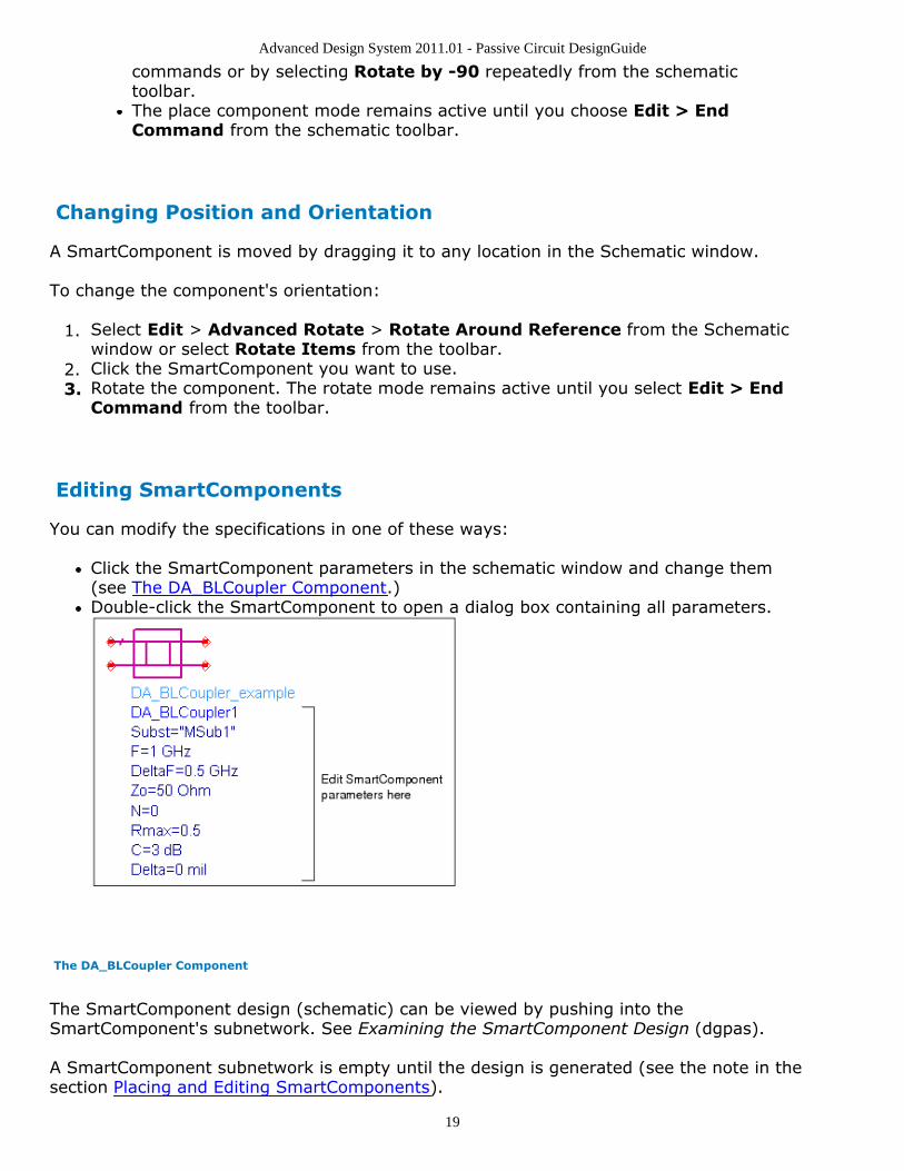
Click the SmartComponent parameters in the schematic window and change them(see The DA_BLCoupler Component.)Double-click the SmartComponent to open a dialog box containing all parameters.
The DA_BLCoupler Component
The SmartComponent design (schematic) can be viewed by pushing into theSmartComponent's subnetwork. See Examining the SmartComponent Design (dgpas).
A SmartComponent subnetwork is empty until the design is generated (see the note in thesection Placing and Editing SmartComponents).
Advanced Design System 2011.01 - Passive Circuit DesignGuide
20
Copying SmartComponentsSmartComponents can be copied within a design, to another design, or to anotherSchematic window.
Copying Within a Schematic
To copy a SmartComponent to the same schematic:
Click the SmartComponent to be copied.1.Select Edit > Copy and then Edit > Paste from the schematic window.2.Click where you want the copy placed.3.
Copying Between Schematic Windows
To copy a SmartComponent to another schematic:
Click the SmartComponent to be copied.1.Select Edit > Copy from the Schematic window.2.Display the design or schematic window you want to copy the SmartComponent to.3.Select Edit > Paste to copy the SmartComponent to the schematic.4.Click where you want the component placed.5.
Copying a SmartComponent as a Unique Design
Initially, all copied SmartComponents refer to the same SmartComponent design. Whenthe Design Assistant is used to perform a design operation, the Design Assistanttransforms each copied SmartComponent into a unique SmartComponent design. A designoperation is accomplished from the Control window.
Deleting SmartComponentsSmartComponents can be deleted from a design like other components, but completelyremoving a SmartComponent's files requires the actions described here.
Deleting from Current Schematic
A SmartComponent can be deleted from a schematic in one of these ways:
By selecting the component and pressing the Delete key.

Advanced Design System 2011.01 - Passive Circuit DesignGuide
21
By selecting Delete from the toolbar.By selecting Edit > Delete from the schematic window.
NoteThis procedure does not remove the SmartComponent files from the workspace directory. To deletefiles from the workspace directory, see Deleting from Current Workspace.
Deleting from Current Workspace
To delete a SmartComponent and all associated files from your workspace:
In the Schematic window, select the SmartComponent.1.In the Control window, select Tools > Delete SmartComponent. or on the toolbar,2.click Delete . This deletes the SmartComponent from the current design andremoves all of its files from your workspace. The SmartComponent delete moderemains active until you select Edit > End Command from the schematic toolbar.
Deleting Manually Using File System
You can use your computer's file system to delete a SmartComponent by deleting theappropriate files in the respective library of a Workspace. Delete files that start with DA_or SA_ , contain the SmartComponent title, and end with . ael, .atf, or .wrk .
Using SmartComponents as Standalone ComponentsAfter SmartComponents are designed and tested, they can be used as standalonecomponents. The DesignGuide is not needed to use them in new designs unless you wishto modify or analyze them. When using the SmartComponent in a design, however, thepower supply pins (Vdd, Vcc, Vp, Vm) must be connected to a DC voltage source whosevoltage level corresponds the parameter setting.
Using an Existing SmartComponent Within the Same Workspace
To use an existing SmartComponent within the same Workspace:
Open the Component Library window by selecting Insert > Component >1.Component Library from the Schematic window or Display Component LibraryList on the toolbar.Select the Library name under All Libraries list at the left of the Component Library2.window. Available components are listed in the Components list at the right of theComponent Library window.Select the SmartComponent in the Components list.3.Place the SmartComponent into your schematic by clicking in the Schematic window4.at the location you wish to place. The insert mode remains active until you click EndCommand.

Advanced Design System 2011.01 - Passive Circuit DesignGuide
22
Using an Existing SmartComponent in Any Workspace
A library of predesigned reusable SmartComponents can be created by placing thereusable SmartComponents in a Workspace. This Workspace can be included in anyWorkspace and its SmartComponents can be accessed using the Component Library.
To use an existing SmartComponent in any Workspace:
Open the Workspace where the SmartComponent needs to be inserted.1.Open the Library in the Workspace by selecting File > Open > Library.2.Open the Component Library window by selecting Insert > Component >3.Component Library from the Schematic window or Display Component LibraryList from the toolbar.Select the Library name under All Libraries list at the left of the Component Library4.window. Available components are listed in the Components list at the right of theComponent Library window.Select the SmartComponent in the Components list.5.Place the SmartComponent into your schematic by clicking in the Schematic window6.at the location where you wish to place the component. The insert mode remainsactive until you click End Command.

Advanced Design System 2011.01 - Passive Circuit DesignGuide
23
Using Automated Assistants in PassiveCircuit DesignGuideThis section describes the Automated Assistants available in this Utility.
Automated Design and AnalysisThe Automated Assistants provide quick design, simulation, yield analysis, andperformance display for SmartComponents and enable transformation of lumped elementsto transmission line elements. Four Automated Assistants are available in this Utility.
Design Assistant is used to generate and update the design contained within aSmartComponent. The Design Assistant invokes a synthesis engine that generates adesign from the given specification. Design Assistant designs and updates a singleSmartComponent or all SmartComponents in a design.
Simulation Assistant is used to analyze the design contained within aSmartComponent. The Simulation Assistant creates a simulation circuit containingthe SmartComponent, then performs a simulation. The Simulation Assistant canautomatically display the results of the simulation.
Optimization Assistant is used to optimize the design contained within aSmartComponent. The Optimization Assistant creates an optimization circuitcontaining the SmartComponent, performs an optimization, and updates theSmartComponent.
Display Assistant is used to easily and quickly display the performance of aSmartComponent. Display templates have been created for most of theSmartComponents. The display templates are preconfigured templates which providea comprehensive look at the component's performance.
Layout Generation. Artwork for all of the passive circuit SmartComponents in thisDesignGuide can be generated automatically. The synthesis engine used by theDesign Assistant creates a schematic for the SmartComponents that is auto-layout-generation ready. The Generate Layout capability of ADS is used to generate theartwork for the SmartComponents.
Explore each tab page by selecting the associated tab on the control window.
Automatic Layout Generation . Artwork for all of the passive circuitSmartComponents in this DesignGuide can be automatically generated. The synthesis

Advanced Design System 2011.01 - Passive Circuit DesignGuide
24
engine used by the Design Assistant creates a schematic for the SmartComponentsthat is auto-layout-generation ready. The Generate Layout capability of ADS is usedto generate the artwork for the SmartComponents. Refer to "Layout Generation" formore information.
Design AssistantThe Design Assistant is used to generate and update the design contained within aSmartComponent from the given specifications. It will design and update a singleSmartComponent or all SmartComponents in a design.
The Design Assistant is accessed using the Passive Circuit DesignGuide Control window.From the Control window, full design control is enabled from the Design Assistant tab.Single component design operations can also be accomplished using the Control windowmenu and toolbar.
Designing a Single Component
To design a single SmartComponent using the Control window, select theSmartComponent either from the SmartComponent drop-down list box in the upper rightcorner of the Control window or by clicking on the component in the Schematic window.The design is accomplished using one of the following methods:
Click the Design button on the Design Assistant tab. The design progress is indicatedon the tab page.Click the Design button on the Control window toolbar.Choose Tools > Auto-Design from the Control window menu.
Designing a Multiple Component
Clicking the Design All button on the Design Assistant tab designs all SmartComponentson the current Schematic. Design progress is indicated on the tab page.
NoteTo avoid screen flicker associated with the design, the Schematic window disappears during the process.
Simulation AssistantThe Simulation Assistant is used to analyze the design contained within aSmartComponent. The Assistant creates a simulation circuit around the SmartComponent,then automatically performs the appropriate simulation. If set, the Assistant automaticallydisplays the simulation results.
The Simulation Assistant is accessed using the Passive Circuit DesignGuide Controlwindow. From the Control window, full simulation control is enabled from the Simulation
Advanced Design System 2011.01 - Passive Circuit DesignGuide
25
Assistant tab. Also, basic simulation can be accomplished using the Control window menuand toolbar.
For all simulation operations, the selected SmartComponent is designed if necessary, asimulation schematic is created, the simulation is performed, and the results aredisplayed. The simulation frequency sweep must be specified on the Simulation Assistanttab in the Control window.
NoteWhen the Simulation Assistant is used, the simulation schematic is deleted automatically. To retain theschematic that is created, instead of the Simulation Assistant, use the Create Template option described inUsing Simulation Templates.
Simulation Frequency Sweep
The simulation frequency sweep is specified on the Passive Circuit DesignGuide Controlwindow. While performing the simulation from the Control window, select the SimulationAssistant tab and specify the sweep by entering the start frequency, stop frequency, andeither frequency step size or number of points. The values entered are stored in theselected SmartComponent (as displayed in the SmartComponent drop-down list box) andare recalled each time this SmartComponent is selected.
NoteIf a SmartComponent has been selected from the SmartComponent drop-down list box on the Controlwindow, default frequencies are set for the component.
Displaying Results Automatically
If you click the Automatically Display Results button on the Control window SimulationAssistant tab, the simulation results are displayed automatically after completion of theanalysis.
Simulating a SmartComponent
To simulate a SmartComponent using the Control window, select the SmartComponenteither from the SmartComponent drop-down list box in the upper right corner of theControl window or by clicking on the component on the schematic window.
The simulation frequency sweep display option must be specified on the SimulationAssistant tab as previously described.
The simulation is then accomplished using one of the following methods:
Click Simulate on the Simulation Assistant tab.Click Simulate on the Control window toolbar.Choose Tools > Auto-Simulate from the Control window menu.
Advanced Design System 2011.01 - Passive Circuit DesignGuide
26
Using Simulation Templates
In some cases, such as when you would like to retain the schematic that is created, youcan simulate the SmartComponent manually.
To generate a simulation schematic around the selected SmartComponent:
Click the Create Template button on the Control window Simulation Assistant tab.1.You can examine or modify the simulation schematic, then manually start the2.simulation by choosing Simulate > Simulate from the Schematic window.When you are finished, click the Update from Template button on the Simulation3.Assistant tab to transfer any changes you have made to the SmartComponent on thesimulation schematic to the original SmartComponent and redesign if necessary.
NoteYou can close the simulation schematic by choosing File > Close Design from the Schematic windowmenu, although this results in loss of any changes you have made to the SmartComponent.
Optimization AssistantThe Optimization Assistant is used to optimize the design contained within aSmartComponent. It creates a optimization circuit containing the SmartComponent, thenperforms an optimization.
The assistant is accessed using the Passive Circuit DesignGuide Control window. From theControl window, full optimization control is enabled from the Optimization Assistant tab.Also, basic optimization can be accomplished using the Control window menu and toolbar.
The Optimization Assistant contains fields that indicate the objective of the optimizationoperation as well as the physical parameters to be altered during the process.
For all optimization operations, the selected SmartComponent is designed (if necessary),an optimization schematic is created, and the optimization is performed. The optimizationresults are transferred to the original SmartComponent, and this altered component isredesigned.
For each component, the optimization alters one or more of the physical designdimensions in order to make the component response more closely meet the specifiedperformance.
Optimizing a SmartComponent
To optimize a SmartComponent using the Control window, follow these steps:
Select the desired SmartComponent either from the SmartComponent drop-down list1.box in the upper right corner of the Control window or by clicking on the componenton the schematic window.Optimize the component by either:2.
Pushing the Optimize button on the Optimization Assistant tab

Advanced Design System 2011.01 - Passive Circuit DesignGuide
27
Pushing the Optimize button on the Control window toolbarSelecting Tools > Auto-Optimize from the Control window menu
Optimization Templates
In some cases it can be useful to manually optimize the SmartComponent.
To generate an optimization schematic around the selected SmartComponent, press theCreate Template button on the Control window Optimization Assistant tab.
You can examine or modify the optimization schematic, then manually start theoptimization by selecting Simulate > Simulate from the Schematic window.
When you are finished, selecting Simulate > Update Optimization Values causes theoptimized values to appear in the VAR element in the schematic for your inspection.
Pressing the Update from Template button on the Optimization Assistant tab transfersthe optimization results to the original SmartComponent and redesign.
NoteYou can manually close the optimization schematic using File > Close Design from the Schematicwindow menu, although this will cause optimization results to be lost.
Display AssistantThe Display Assistant is used to display the performance of a SmartComponent. Thedisplay templates are preconfigured display files that provide a comprehensive look at theperformance of the component. You can create your own displays or modify the displaytemplates included using the built in features of Advanced Design System. In mostsituations, the display templates included provide all the information you need.
The Display Assistant is accessed using the Passive Circuit DesignGuide Control window.From the Control window, full display control is enabled from the Display Assistant tab.Basic display selection can also be accomplished using the Control window menu andtoolbar.
Display Templates
The display templates are preconfigured templates that provide a comprehensive look atthe performance of the component. Display templates have been created for most of theSmartComponents.
This includes all of the RLC, coupler, filter and matching components. The line componentsdo not have auto-simulation, auto-optimization or auto-display capability because of theirsimplicity.
You can create your own displays or modify the included display templates using the built
Advanced Design System 2011.01 - Passive Circuit DesignGuide
28
in features of Advanced Design System, but in most situations, the display templatesincluded provide all the information you need.
The display templates opened by the Display Assistant have common features that arediscussed here. For features unique to the display templates of some SmartComponents,refer to SmartComponent Reference (dgfilter).
Also, in some cases you can use one of the display templates provided with theDesignGuide for other applications.
To open one of these templates, select the template from the Available Templates fieldand press the Open Display Template button on the Control window Display Assistanttab.
Then you can insert a dataset of your choice using the dataset pull-down list box in theupper left corner of the display. If you find that some parameters in the display templateare not defined in the selected dataset, you can make appropriate modifications to thedisplay. These changes can be saved using the commands in the display File menu.
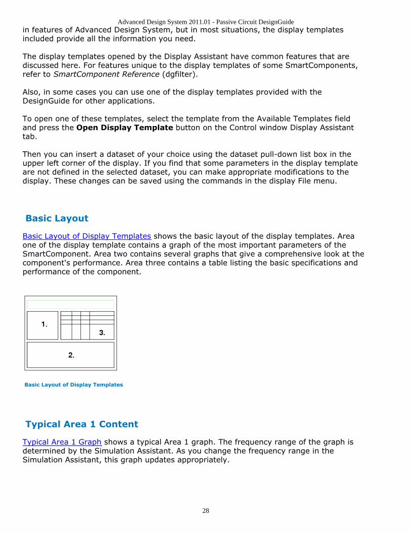
Basic Layout
Basic Layout of Display Templates shows the basic layout of the display templates. Areaone of the display template contains a graph of the most important parameters of theSmartComponent. Area two contains several graphs that give a comprehensive look at thecomponent's performance. Area three contains a table listing the basic specifications andperformance of the component.
Basic Layout of Display Templates
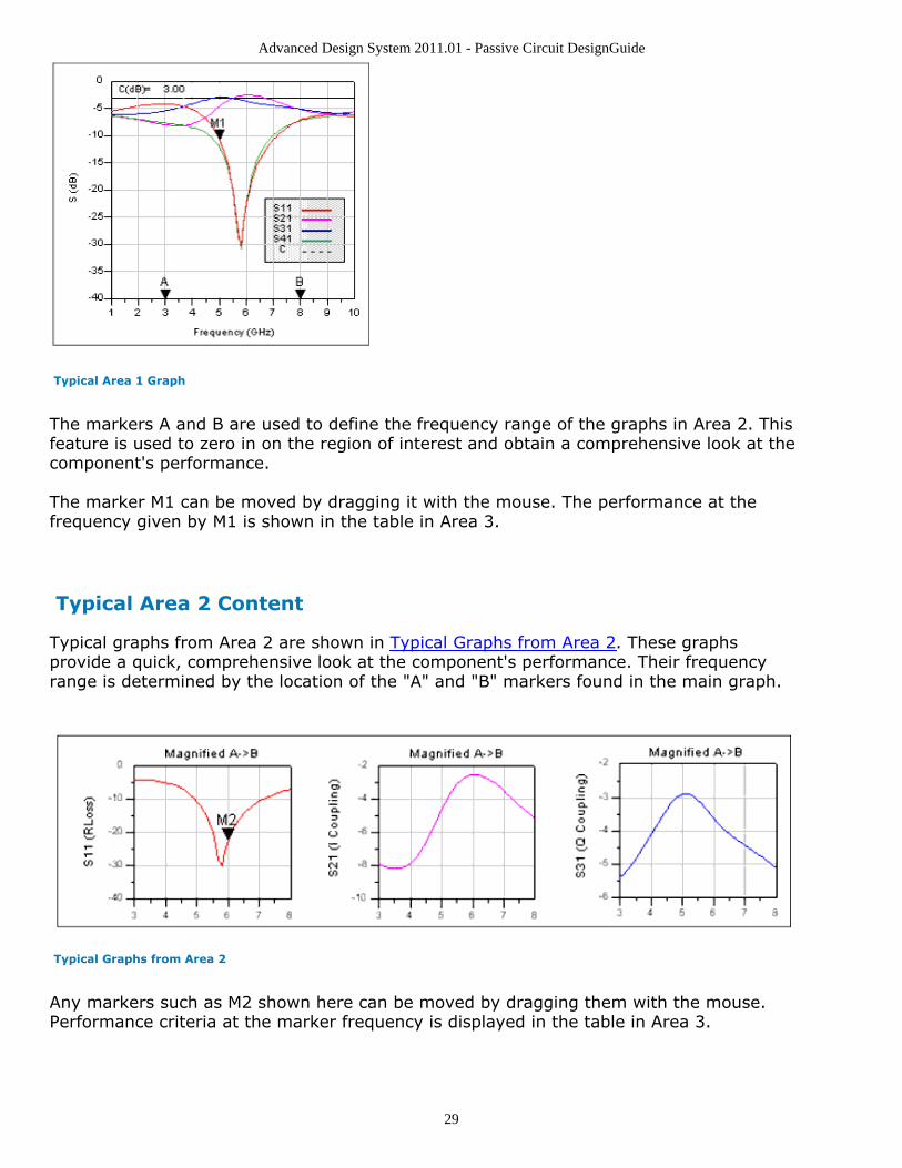
Typical Area 1 Content
Typical Area 1 Graph shows a typical Area 1 graph. The frequency range of the graph isdetermined by the Simulation Assistant. As you change the frequency range in theSimulation Assistant, this graph updates appropriately.
Advanced Design System 2011.01 - Passive Circuit DesignGuide
29
Typical Area 1 Graph
The markers A and B are used to define the frequency range of the graphs in Area 2. Thisfeature is used to zero in on the region of interest and obtain a comprehensive look at thecomponent's performance.
The marker M1 can be moved by dragging it with the mouse. The performance at thefrequency given by M1 is shown in the table in Area 3.
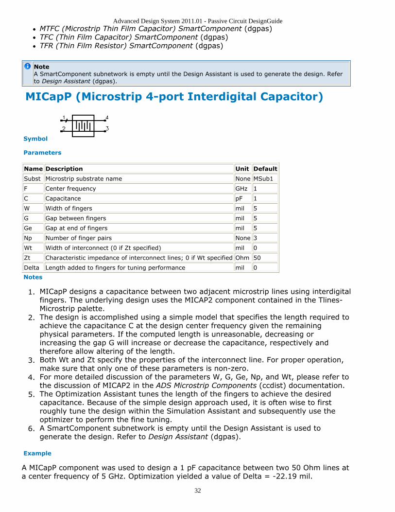
Typical Area 2 Content
Typical graphs from Area 2 are shown in Typical Graphs from Area 2. These graphsprovide a quick, comprehensive look at the component's performance. Their frequencyrange is determined by the location of the "A" and "B" markers found in the main graph.
Typical Graphs from Area 2
Any markers such as M2 shown here can be moved by dragging them with the mouse.Performance criteria at the marker frequency is displayed in the table in Area 3.

Advanced Design System 2011.01 - Passive Circuit DesignGuide
30
Typical Area 3 Content
A typical table from Area 3 is shown in Typical Table from Area 3. The white rows showthe desired specifications and important performance criteria for the component. The grayrows give the performance criteria at the user defined marker frequencies. The box belowthe table provides explanatory information for the table.
Typical Table from Area 3
Displaying SmartComponent Performance Results
Before using the Display Assistant, a valid dataset from a simulation of the selectedSmartComponent must exist in the current workspace data directory. This simulation canbe conveniently accomplished using the Simulation Assistant. Refer to SimulationAssistant for details on this step.
To display results from a SmartComponent simulation using the Control window, selectthe SmartComponent either from the SmartComponent drop-down list box in the upperright corner of the Control window or by clicking on the component on the schematicwindow. The display is then launched using one of the following methods:
Push the Display button on the Display Assistant tab.Push the Display button on the Control window toolbar.Select Tools > Auto-Display from the Control window menu.
If no valid dataset exists for the selected SmartComponent, the Display button on theDisplay Assistant tab is insensitive. If the toolbar or menu are used to try to display the

Advanced Design System 2011.01 - Passive Circuit DesignGuide
31
results, a message appears indicating that no dataset exists.
Layout GenerationThe Design Assistant creates a schematic for the SmartComponents that is ready for auto-layout generation. Artwork for all of the Passive Circuit DesignGuide SmartComponentscan be automatically generated. The ADS Generate Layout capability is used to generatethe artwork for the SmartComponents.
NoteYou need an Advanced Design System Layout license to use this feature.
Creating Layout Artwork
To create artwork for SmartComponents, follow these steps:
Choose and place the SmartComponents in the schematic window.1.Specify the parameters for each SmartComponent.2.Design the SmartComponents using the Design Assistant.3.Select Layout > Generate/Update Layout from the Schematic window.4.Choose OK in the Generate/Update Layout box.5.
The artwork for each SmartComponent and any other components that have associatedartwork is displayed in the Layout window. If the status report checkbox is selected in theGenerate/Update Layout box, a layout generation status report opens also.
Updating Layout Artwork
To edit the properties of a SmartComponent and update the associated artwork, followthese steps:
Choose the SmartComponent in the schematic window.1.Edit the parameters of the SmartComponent.2.Design the SmartComponent using the Design Assistant.3.Select Layout > Generate/Update Layout from the Schematic window.4.Select OK in the Generate/Update Layout box.5.
The artwork for the SmartComponent is updated and displays in the layout window.
Passive RLC ComponentsMICapP (Microstrip 4-port Interdigital Capacitor) (dgpas)MICapPG (Microstrip Grounded 2-port Interdigital Capacitor) (dgpas)MICapS (Microstrip 2-port Interdigital Capacitor) (dgpas)MICapSG (Microstrip 1-port Interdigital Capacitor) (dgpas)MREInd (Microstrip Elevated Rectangular Inductor) (dgpas)MRInd (Microstrip Rectangular Inductor) SmartComponent (dgpas)MSInd (Microstrip Spiral Inductor) (dgpas)
Advanced Design System 2011.01 - Passive Circuit DesignGuide
32
MTFC (Microstrip Thin Film Capacitor) SmartComponent (dgpas)TFC (Thin Film Capacitor) SmartComponent (dgpas)TFR (Thin Film Resistor) SmartComponent (dgpas)
NoteA SmartComponent subnetwork is empty until the Design Assistant is used to generate the design. Referto Design Assistant (dgpas).
MICapP (Microstrip 4-port Interdigital Capacitor)
Symbol
Parameters
Name Description Unit Default
Subst Microstrip substrate name None MSub1
F Center frequency GHz 1
C Capacitance pF 1
W Width of fingers mil 5
G Gap between fingers mil 5
Ge Gap at end of fingers mil 5
Np Number of finger pairs None 3
Wt Width of interconnect (0 if Zt specified) mil 0
Zt Characteristic impedance of interconnect lines; 0 if Wt specified Ohm 50
Delta Length added to fingers for tuning performance mil 0
Notes
MICapP designs a capacitance between two adjacent microstrip lines using interdigital1.fingers. The underlying design uses the MICAP2 component contained in the Tlines-Microstrip palette.The design is accomplished using a simple model that specifies the length required to2.achieve the capacitance C at the design center frequency given the remainingphysical parameters. If the computed length is unreasonable, decreasing orincreasing the gap G will increase or decrease the capacitance, respectively andtherefore allow altering of the length.Both Wt and Zt specify the properties of the interconnect line. For proper operation,3.make sure that only one of these parameters is non-zero.For more detailed discussion of the parameters W, G, Ge, Np, and Wt, please refer to4.the discussion of MICAP2 in the ADS Microstrip Components (ccdist) documentation.The Optimization Assistant tunes the length of the fingers to achieve the desired5.capacitance. Because of the simple design approach used, it is often wise to firstroughly tune the design within the Simulation Assistant and subsequently use theoptimizer to perform the fine tuning.A SmartComponent subnetwork is empty until the Design Assistant is used to6.generate the design. Refer to Design Assistant (dgpas).
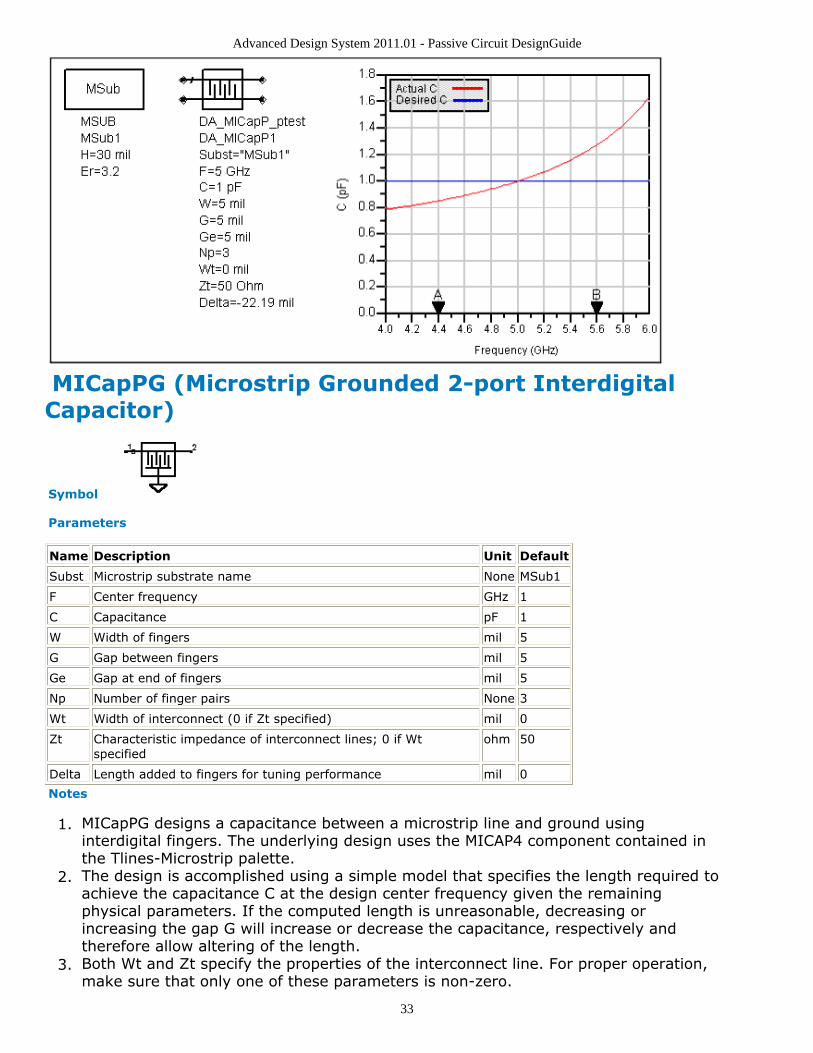
Example
A MICapP component was used to design a 1 pF capacitance between two 50 Ohm lines ata center frequency of 5 GHz. Optimization yielded a value of Delta = -22.19 mil.
Advanced Design System 2011.01 - Passive Circuit DesignGuide
33
MICapPG (Microstrip Grounded 2-port InterdigitalCapacitor)
Symbol
Parameters
Name Description Unit Default
Subst Microstrip substrate name None MSub1
F Center frequency GHz 1
C Capacitance pF 1
W Width of fingers mil 5
G Gap between fingers mil 5
Ge Gap at end of fingers mil 5
Np Number of finger pairs None 3
Wt Width of interconnect (0 if Zt specified) mil 0
Zt Characteristic impedance of interconnect lines; 0 if Wtspecified
ohm 50
Delta Length added to fingers for tuning performance mil 0
Notes
MICapPG designs a capacitance between a microstrip line and ground using1.interdigital fingers. The underlying design uses the MICAP4 component contained inthe Tlines-Microstrip palette.The design is accomplished using a simple model that specifies the length required to2.achieve the capacitance C at the design center frequency given the remainingphysical parameters. If the computed length is unreasonable, decreasing orincreasing the gap G will increase or decrease the capacitance, respectively andtherefore allow altering of the length.Both Wt and Zt specify the properties of the interconnect line. For proper operation,3.make sure that only one of these parameters is non-zero.

Advanced Design System 2011.01 - Passive Circuit DesignGuide
34
For more detailed discussion of the parameters W, G, Ge, Np, and Wt, please refer to4.the discussion of MICAP4 in the ADS Microstrip Components (ccdist) documentation.The Optimization Assistant tunes the length of the fingers to achieve the desired5.capacitance. Because of the simple design approach used, it is often wise to firstroughly tune the design within the Simulation Assistant and subsequently use theoptimizer to perform the fine tuning.A SmartComponent subnetwork is empty until the Design Assistant is used to6.generate the design. Refer to Design Assistant (dgpas).
Example
A MICapPG component was used to design a 1 pF capacitance from a 50 Ohm microstripline and ground at a center frequency of 5 GHz. Optimization yielded a value of Delta = -21.355 mil.
MICapS (Microstrip 2-port Interdigital Capacitor)
Symbol
Parameters

Advanced Design System 2011.01 - Passive Circuit DesignGuide
35
Name Description Unit Default
Subst Microstrip substrate name None MSub1
F Center frequency GHz 1
C Capacitance pF 1
W Width of fingers mil 5
G Gap between fingers mil 5
Ge Gap at end of fingers mil 5
Np Number of finger pairs None 3
Wt Width of interconnect (0 if Zt specified) mil 25
Wf Width of feed line (0 if Zf specified) mil 0
Zf Characteristic impedance of feed line; 0 if Wt specified Ohm 50
Delta Length added to fingers for tuning performance mil 0
Notes
MICapS designs a series capacitance within a microstrip line using interdigital fingers.1.The underlying design uses the MICAP1 component contained in the Tlines-Microstrippalette.The design is accomplished using a simple model that specifies the length required to2.achieve the capacitance C at the design center frequency given the remainingphysical parameters. If the computed length is unreasonable, decreasing orincreasing the gap G will increase or decrease the capacitance, respectively andtherefore allow altering of the length.Both Wf and Zf specify the properties of the feed line. For proper operation, make3.sure that only one of these parameters is non-zero.For more detailed discussion of the parameters W, G, Ge, Np, Wt, and Wf, please4.refer to the discussion of MICAP1 in the ADS Microstrip Components (ccdist)documentation.The Optimization Assistant tunes the length of the fingers to achieve the desired5.capacitance. Because of the simple design approach used, it is often wise to firstroughly tune the design within the Simulation Assistant and subsequently use theoptimizer to perform the fine tuning.A SmartComponent subnetwork is empty until the Design Assistant is used to6.generate the design. Refer to Design Assistant (dgpas).
Example
A MICapS component was used to design a 1 pF series capacitance for a 50 Ohm line at acenter frequency of 5 GHz. Optimization yielded a value of Delta = 2.443 mil.

Advanced Design System 2011.01 - Passive Circuit DesignGuide
36
MICapSG (Microstrip 1-port Interdigital Capacitor)
Symbol
Parameters
Name Description Unit Default
Subst Microstrip substrate name None MSub1
F Center frequency GHz 1
C Capacitance pF 1
W Width of fingers mil 5
G Gap between fingers mil 5
Ge Gap at end of fingers mil 5
Np Number of finger pairs None 3
Wt Width of interconnect mil 25
Wf Width of feed line (0 if Zf specified) mil 0
Zf Characteristic impedance of feed line; 0 if Wfspecified
Ohm 50
Delta Length added to fingers for tuning performance mil 0
Notes
MICapSG designs a series capacitance between a microstrip line and ground using1.interdigital fingers. The underlying design uses the MICAP3 component contained inthe Tlines-Microstrip palette.The design is accomplished using a simple model that specifies the length required to2.achieve the capacitance C at the design center frequency given the remainingphysical parameters. If the computed length is unreasonable, decreasing orincreasing the gap G will increase or decrease the capacitance, respectively andtherefore allow altering of the length.Both Wf and Zf specify the properties of the feed line. For proper operation, make3.sure that only one of these parameters is non-zero.

Advanced Design System 2011.01 - Passive Circuit DesignGuide
37
For more detailed discussion of the parameters W, G, Ge, Np, Wt, and Wf, please4.refer to the discussion of MICAP3 in the ADS Microstrip Components (ccdist)documentation.The Optimization Assistant tunes the length of the fingers to achieve the desired5.capacitance. Because of the simple design approach used, it is often wise to firstroughly tune the design within the Simulation Assistant and subsequently use theoptimizer to perform the fine tuning.A SmartComponent subnetwork is empty until the Design Assistant is used to6.generate the design. Refer to Design Assistant (dgpas).
Example
A MICapSG component was used to design a 1 pF capacitance for a 50 Ohm line at acenter frequency of 5 GHz. Optimization yielded a value of Delta = -1.841 mil.
MREInd (Microstrip Elevated Rectangular Inductor)
Symbol
Parameters

Advanced Design System 2011.01 - Passive Circuit DesignGuide
38
Name Description Unit Default
Subst Microstrip substrate name None MSub1
F Center frequency GHz 1
L Inductance nH 1
Ln Length of innermost segment (0 means full length) mil 0
Ln1 Length of second innermost segment mil 2.5
Ln2 Length of second innermost segment mil 3.5
W Conductor width mil 1
S Conductor spacing mil 1
Hi Elevation of inductor above substrate mil 12.5
Ti Thickness of conductors mil 0.1
Ri resistivity (relative to gold) of conductors None 1
Sx spacing limit between support posts (0 to ignore posts) mil 0
Cc coefficient for capacitance of corner support posts None 2
Cs coefficient for capacitance of support posts along segment None 1
Wu width of underpass strip conductor mil 0.4
Au angle of departure from innermost segment None 0
UE extension of underpass beyond inductor mil 4
Delta incremental number of segments for tuning inductance (need not be integer) None 0
Notes
MREInd designs an elevated microstrip rectangular inductor. The underlying design1.uses the MRINDELA component contained in the Tlines-Microstrip palette.The design is accomplished using a simple model that specifies the number of2.segments in the rectangular inductor required to achieve the inductance L at thedesign center frequency given the remaining physical parameters.The parameters from Hi through Cs are not actually used in the design process, and3.therefore final tuning is required to achieve the proper value of the inductance.The tuning parameter Delta represents the number of additional segments to add to4.the outside of the structure. If it is not an integer value, the outermost segment (L1)will not be full length, with the fractional remainder of Delta specifying the fractionallength of this outermost segment. The design process may not produce theparameters that perfectly achieve the specified inductance. Manual tuning of theinductance can be performed by specifying the parameter Delta, which representsthe number of turns to add to the design. For example, if the design processdetermines that the number of required turns is 1.2 and Delta is set to 0.3, theactual number of turns in the underlying inductor design will be 1.2+0.3=1.5. Deltacan be positive or negative and, as shown in this example, need not be an integer.The values Ln, Ln1, and Ln2 represent the lengths Ln, Ln-1, and Ln-2 associated with5.the MRINDELA component. For more detailed discussion of these lengths as well asthe parameters from W through UE, please refer to the discussion of MRINDELA inthe ADS Microstrip Components (ccdist) documentation.Because of the difficulties associated with tuning the inductor using additional6.discrete segments, no Optimization Assistant is provided. However, tuning can beaccomplished quite effectively by manually updating the value of Delta from withinthe Simulation Assistant. Refer to Simulation Assistant (dgpas), as well as thefollowing example for more details.A SmartComponent subnetwork is empty until the Design Assistant is used to7.generate the design. Refer to Design Assistant (dgpas).
Example
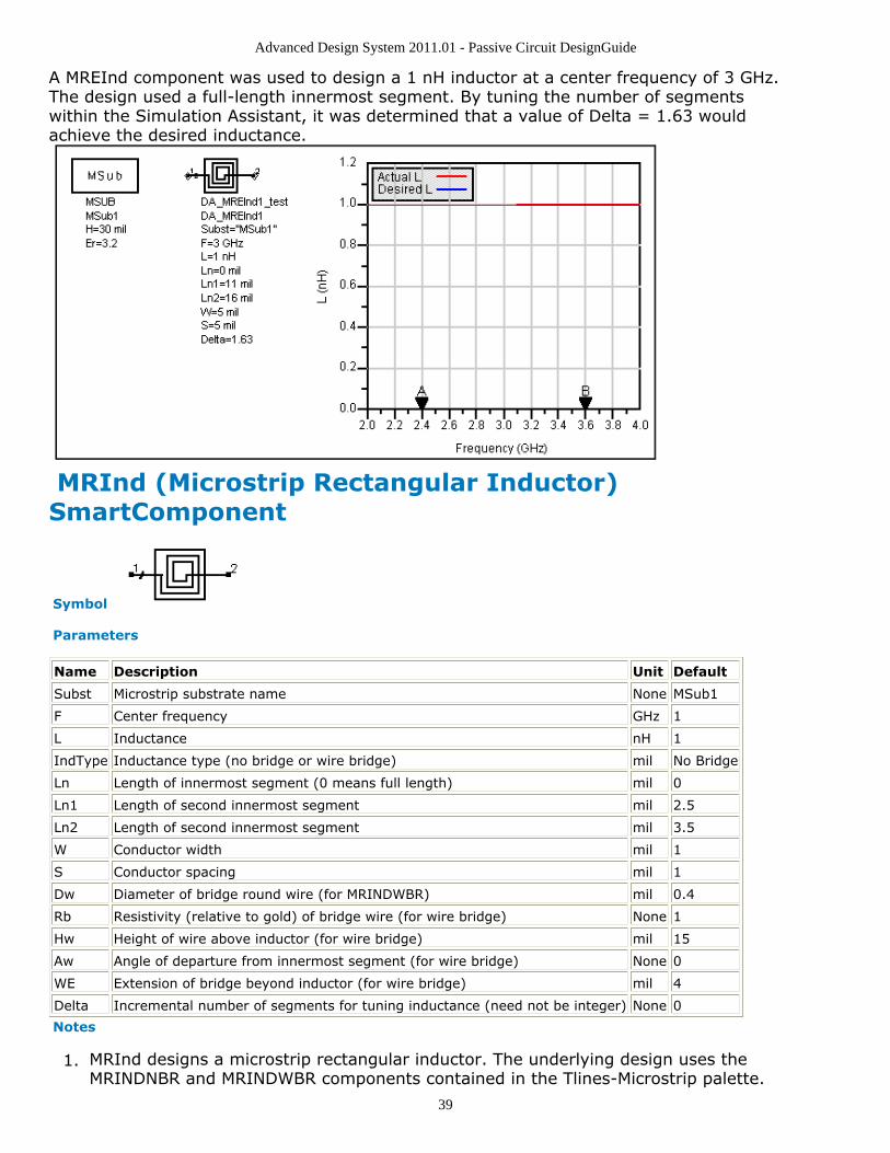
Advanced Design System 2011.01 - Passive Circuit DesignGuide
39
A MREInd component was used to design a 1 nH inductor at a center frequency of 3 GHz.The design used a full-length innermost segment. By tuning the number of segmentswithin the Simulation Assistant, it was determined that a value of Delta = 1.63 wouldachieve the desired inductance.
MRInd (Microstrip Rectangular Inductor)SmartComponent
Symbol
Parameters
Name Description Unit Default
Subst Microstrip substrate name None MSub1
F Center frequency GHz 1
L Inductance nH 1
IndType Inductance type (no bridge or wire bridge) mil No Bridge
Ln Length of innermost segment (0 means full length) mil 0
Ln1 Length of second innermost segment mil 2.5
Ln2 Length of second innermost segment mil 3.5
W Conductor width mil 1
S Conductor spacing mil 1
Dw Diameter of bridge round wire (for MRINDWBR) mil 0.4
Rb Resistivity (relative to gold) of bridge wire (for wire bridge) None 1
Hw Height of wire above inductor (for wire bridge) mil 15
Aw Angle of departure from innermost segment (for wire bridge) None 0
WE Extension of bridge beyond inductor (for wire bridge) mil 4
Delta Incremental number of segments for tuning inductance (need not be integer) None 0
Notes
MRInd designs a microstrip rectangular inductor. The underlying design uses the1.MRINDNBR and MRINDWBR components contained in the Tlines-Microstrip palette.

Advanced Design System 2011.01 - Passive Circuit DesignGuide
40
The design is accomplished using a simple model that specifies the number of2.segments in the rectangular inductor required to achieve the inductance L at thedesign center frequency given the remaining physical parameters.The parameters Rb and Hw are not actually used in the design process, and therefore3.final tuning is required to achieve the proper value of the inductance.The value of IndType specifies the type of inductor that will be designed. If this4.parameter is set to "No Bridge", then the MRINDNBR component is designed and theparameters from Dw to WE are ignored. If the parameter is set to "Wire Bridge", thenthe MRINDWBR component is designed and the parameters from Dw to WE are used.The tuning parameter Delta represents the number of additional segments to add to5.the outside of the structure. If it is not an integer value, the outermost segment (L1)will not be full length, with the fractional remainder of Delta specifying the fractionallength of this outermost segment. The design process may not produce theparameters that perfectly achieve the specified inductance. Manual tuning of theinductance can be performed by specifying the parameter Delta, which representsthe number of turns to add to the design. For example, if the design processdetermines that the number of required turns is 1.2 and Delta is set to 0.3, theactual number of turns in the underlying inductor design will be 1.2+0.3=1.5. Deltacan be positive or negative and, as shown in this example, need not be an integer.The values Ln, Ln1, and Ln2 represent the lengths Ln, Ln-1, and Ln-2 associated with6.the MRINDNBR and MRINDWBR components. For more detailed discussion of theselengths as well as the parameters W through WE, please refer to the discussion ofthese components in the ADS Microstrip Components (ccdist) documentation.Because of the difficulties associated with tuning the inductor using additional7.discrete segments, no Optimization Assistant is provided. However, tuning can beaccomplished quite effectively by manually updating the value of Delta from withinthe Simulation Assistant, refer to Simulation Assistant (dgpas), as well as thefollowing example for more details.A SmartComponent subnetwork is empty until the Design Assistant is used to8.generate the design. Refer to Design Assistant (dgpas).
Example
A MRInd component with no bridge was used to design a 1 nH inductor at a centerfrequency of 3 GHz. The design used a full-length innermost segment. By tuning thenumber of segments within the Simulation Assistant, it was determined that a value ofDelta = 0.52 would achieve the desired inductance.

Advanced Design System 2011.01 - Passive Circuit DesignGuide
41
MSInd (Microstrip Spiral Inductor)
Symbol
Parameters
Name Description Unit Default
Subst Microstrip substrate name None MSub1
F Center frequency GHz 1
L Inductance nH 10
Ri Inner radius measured to center of conductor mil 50
W Conductor width mil 10
S Conductor spacing mil 10
W1 Width of strip connected to pin 1 mil 10
W2 Width of strip connected to pin 2 mil 10
Delta Incremental number of turns for tuning inductance (need not beinteger)
None 0
Notes
MSInd designs a microstrip spiral inductor. The underlying design uses the MSIND1.component contained in the Tlines-Microstrip palette.The design is accomplished using a simple model that specifies the number of turns2.in the spiral inductor required to achieve the inductance L at the design centerfrequency given the remaining physical parameters.The value of Ri specifies the distance from the center of the inductor to the center of3.the conductor at its innermost point in the spiral. Refer to the discussion of theMSIND component in the ADS Microstrip Components (ccdist) documentation for amore detailed discussion of this parameter.The tuning parameter Delta represents the number of additional turns to add to the4.outside of the structure. Fractional numbers of turns are accommodated (i.e. Deltaneed not be an integer value). The design process may not produce the parametersthat perfectly achieve the specified inductance. Manual tuning of the inductance can
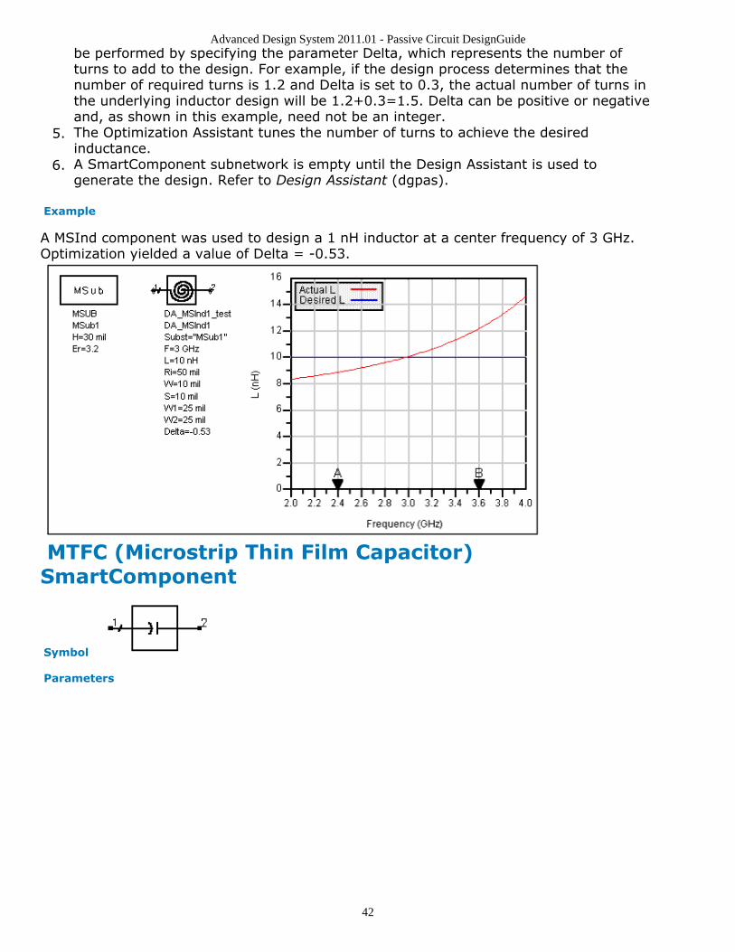
Advanced Design System 2011.01 - Passive Circuit DesignGuide
42
be performed by specifying the parameter Delta, which represents the number ofturns to add to the design. For example, if the design process determines that thenumber of required turns is 1.2 and Delta is set to 0.3, the actual number of turns inthe underlying inductor design will be 1.2+0.3=1.5. Delta can be positive or negativeand, as shown in this example, need not be an integer.The Optimization Assistant tunes the number of turns to achieve the desired5.inductance.A SmartComponent subnetwork is empty until the Design Assistant is used to6.generate the design. Refer to Design Assistant (dgpas).
Example
A MSInd component was used to design a 1 nH inductor at a center frequency of 3 GHz.Optimization yielded a value of Delta = -0.53.
MTFC (Microstrip Thin Film Capacitor)SmartComponent
Symbol
Parameters
Advanced Design System 2011.01 - Passive Circuit DesignGuide
43
Name Description Unit Default
Subst Microstrip substrate name None MSub1
F Center frequency GHz 1
C Capacitance pF 1
W Conductor width; set to 0 if Zo specified mil 0
Zo Characteristic impedance of line for computing W; set to 0 if W specified Ohm 50
CPUA Capacitance per unit area pf/mm2 300
T Thickness of capacitor dielectric mil 0.2
RsT Sheet resistance of top metal plate Ohm 0
RsB Sheet resistance of bottom metal plate Ohm 0
TT Thickness of top metal plate mil 0
TB Thickness of bottom metal plate mil 0
COB Bottom conductor overlap mil 0
COT Top conductor overlap mil 0
DO Dielectric overlap mil 0
Delta Length added to conductor for tuning capacitance mil 0
Notes
MTFC designs a microstrip thin film capacitor. The underlying design uses the MTFC1.component contained in the Tlines-Microstrip palette.The design is accomplished by determining the length required to achieve the desired2.capacitance using the capacitance per unit area (CPUA) in conjunction with thespecified width (W).Since this capacitor is often fed with a microstrip line, either the physical width or the3.characteristic impedance of a microstrip line on the substrate can be specified.However, only one of the parameters should be non-zero.The parameters from RsT through DO inclusive are not used in the design process4.but are passed on to the underlying MTFC component and therefore included in anysimulations or optimizations.The tuning parameter Delta represents incremental length required to achieve the5.desired capacitance. It is typically relatively small, as the initial design tends to beaccurate.The Optimization Assistant tunes the conductor length to achieve the desired6.capacitance.A SmartComponent subnetwork is empty until the Design Assistant is used to7.generate the design. Refer to Design Assistant (dgpas).
Example
A MTFC component was used to design a 100 pF capacitor at a center frequency of 2 GHz.The conductor width corresponds to that of a 50 Ohm microstrip line fabricated on MSub1.Optimization yielded a value of Delta = -2.411.

Advanced Design System 2011.01 - Passive Circuit DesignGuide
44
TFC (Thin Film Capacitor) SmartComponent
Symbol
Parameters
Name Description Unit Default
F Center frequency GHz 1
C Capacitance pF 1
W Conductor width mil 25
T Thickness of capacitor dielectric mil 0.2
Er Relative dielectric constant None 9.6
Rho Resistivity of conductor (relative to gold) None 1
TanD Dielectric loss tangent None 0
CO Conductor overlap mil 0
DO Dielectric overlap mil 0
Delta Length added to conductor for tuning capacitance mil 0
Notes
TFC designs a thin film capacitor. The underlying design uses the TFC component1.contained in the Tlines-Microstrip palette.The design is accomplished by determining the length required to achieve the desired2.capacitance using the simple parallel plate capacitor model C = Er*W*L/T. Theparameters from Rho through DO inclusive are not used in the design process but arepassed on to the underlying TFC component and are therefore included in anysimulations or optimizations.The tuning parameter Delta represents incremental length required to achieve the3.desired capacitance. It is typically relatively small, as the initial design tends to beaccurate.The Optimization Assistant tunes the conductor length to achieve the desired4.capacitance.A SmartComponent subnetwork is empty until the Design Assistant is used to5.
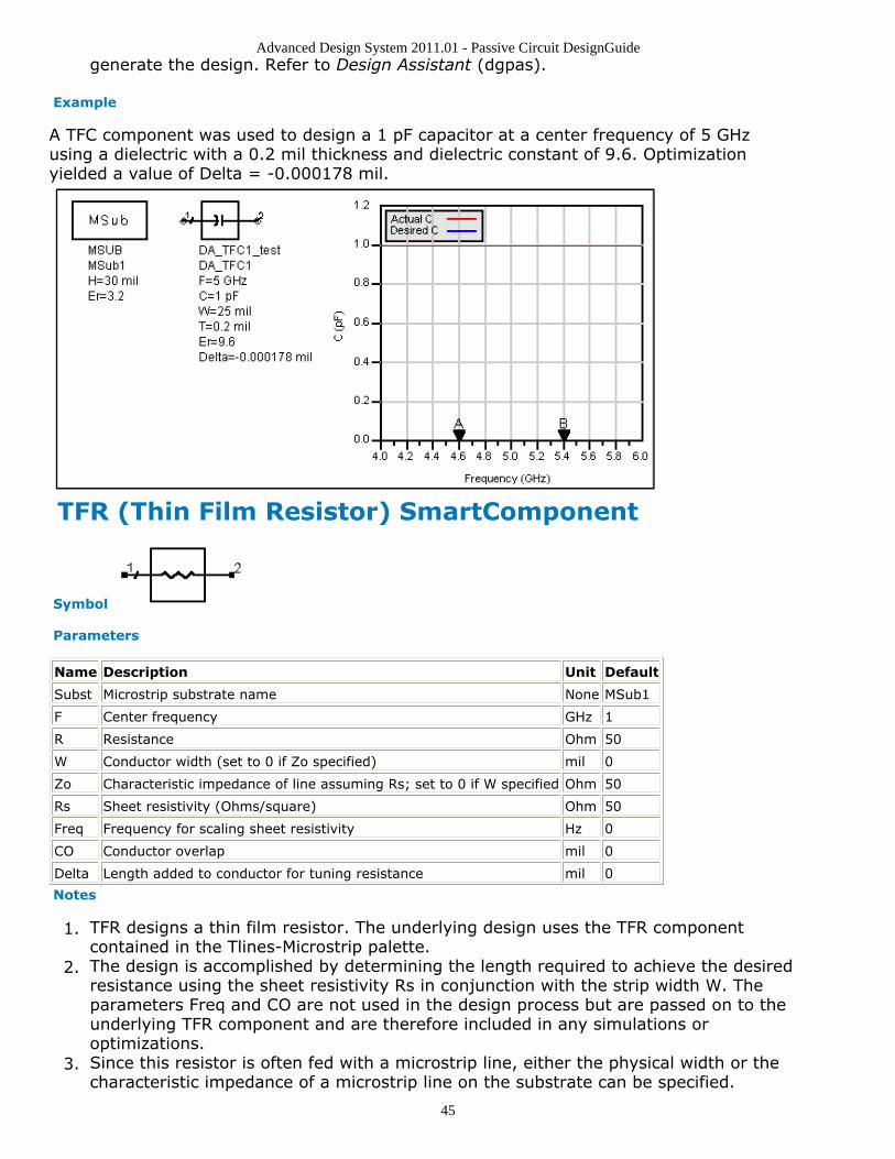
Advanced Design System 2011.01 - Passive Circuit DesignGuide
45
generate the design. Refer to Design Assistant (dgpas).
Example
A TFC component was used to design a 1 pF capacitor at a center frequency of 5 GHzusing a dielectric with a 0.2 mil thickness and dielectric constant of 9.6. Optimizationyielded a value of Delta = -0.000178 mil.
TFR (Thin Film Resistor) SmartComponent
Symbol
Parameters
Name Description Unit Default
Subst Microstrip substrate name None MSub1
F Center frequency GHz 1
R Resistance Ohm 50
W Conductor width (set to 0 if Zo specified) mil 0
Zo Characteristic impedance of line assuming Rs; set to 0 if W specified Ohm 50
Rs Sheet resistivity (Ohms/square) Ohm 50
Freq Frequency for scaling sheet resistivity Hz 0
CO Conductor overlap mil 0
Delta Length added to conductor for tuning resistance mil 0
Notes
TFR designs a thin film resistor. The underlying design uses the TFR component1.contained in the Tlines-Microstrip palette.The design is accomplished by determining the length required to achieve the desired2.resistance using the sheet resistivity Rs in conjunction with the strip width W. Theparameters Freq and CO are not used in the design process but are passed on to theunderlying TFR component and are therefore included in any simulations oroptimizations.Since this resistor is often fed with a microstrip line, either the physical width or the3.characteristic impedance of a microstrip line on the substrate can be specified.
Advanced Design System 2011.01 - Passive Circuit DesignGuide
46
The tuning parameter Delta represents incremental length required to achieve the4.desired resistance.The Optimization Assistant tunes the conductor length to achieve the desired5.resistance.A SmartComponent subnetwork is empty until the Design Assistant is used to6.generate the design. Refer to Design Assistant (dgpas).
Example
A TFR component was used to design a 50 Ohm resistor at a center frequency of 5 GHzusing a conductor with a sheet resistance of 50 Ohm/square. The conductor width waschosen to correspond to that of a 50 Ohm microstrip line on the substrate. Optimizationyielded a value of Delta = -3.549 mil.
Passive Microstrip ComponentsMBend (Microstrip Bend Component) (dgpas)MBStub (Microstrip Butterfly Radial Stub) (dgpas)MCFil (Microstrip Coupled-Line Filter Element) (dgpas)MCLine (Microstrip Coupled Line Component) (dgpas)MCorn (Microstrip Corner Component) (dgpas)MCross (Microstrip Cross Component) (dgpas)MCurve (Microstrip Curve Component) (dgpas)MGap (Microstrip Gap Component) (dgpas)MLine (Microstrip Line) (dgpas)MMndr (Microstrip Meander Line) (dgpas)MRStub (Microstrip Radial Stub) SmartComponent (dgpas)MStep (Microstrip Step Component) (dgpas)MStub (Microstrip Stub) (dgpas)MTaper (Microstrip Taper Component) (dgpas)MTee (Microstrip Tee Component) (dgpas)
NoteA SmartComponent subnetwork is empty until the Design Assistant is used to generate the design. Referto Design Assistant (dgpas).
MBend (Microstrip Bend Component)

Advanced Design System 2011.01 - Passive Circuit DesignGuide
47
Symbol
Parameters
Name Description Unit Default
Subst Microstrip substrate name None MSub1
F Design frequency GHz 1
Zo Desired characteristic impedance Ohm 50
BendType Type of bend None Arbitrary
Angle Angle of bend (for arbitrary angle/miter bend) None 90
M Miter fraction (for arbitrary angle/miter bend) None 0.6
Notes
MBend designs a microstrip bend given the substrate, desired characteristic1.impedance, and bend properties. The design realizes the native MBEND, MBEND2, orMBEND3 components.Since the design uses the models inherent to ADS to compute the line width, there is2.no need for a dedicated Simulation Assistant, Optimization Assistant, or DisplayAssistant.BendType can be Arbitrary Angle/Miter (MBEND), 90 Degree/Miter (MBEND2), or 903.Degree/Optimal Miter (MBEND3). The parameters Angle and M are only used forMBEND realizations. Refer to the discussion of these components in the ADSMicrostrip Components (ccdist) documentation for a more detailed description.A SmartComponent subnetwork is empty until the Design Assistant is used to4.generate the design. Refer to Design Assistant (dgpas).
MBStub (Microstrip Butterfly Radial Stub)
Symbol
Parameters
Name Description Unit Default
Subst Microstrip substrate name None MSub1
F Design frequency GHz 1
Xin Input reactance0 Ohm 0†
Cin Input capacitance pF 0†
Lin Input inductance nH 0†
W Width of feed line; set to zero if Z specified mil 0
Z Characteristic impedance of feed line; set to zero if Z specified Ohm 50
Angle Subtended angle of circular sector None 60
D Insertion depth of circular sector in feed line mil 3
Delta Length added to stub for tuning performance mil 0
† Only one of Xin, Cin, and Lin can be non-zero Notes

Advanced Design System 2011.01 - Passive Circuit DesignGuide
48
MBStub designs a microstrip butterfly radial stub given the substrate, desired input1.reactance, and stub dimensions.The stub is designed by dividing the radial lines into several short segments.2.For proper operation, only one of Xin, Cin, and Lin can be non-zero. If all are zero,3.the stub is designed to provide an open circuit.Refer to the discussion of the MBSTUB component in the ADS Microstrip Components4.(ccdist) documentation for a more detailed description of the model used for thiscomponent.The optimization changes the length of the stubs to achieve the desired input5.reactance.A SmartComponent subnetwork is empty until the Design Assistant is used to6.generate the design. Refer to Design Assistant (dgpas).
Example
A MBStub component was used to design an open circuit stub at a center frequency of 1GHz. Optimization yielded a value of Delta = 88.786 mil.
MCFil (Microstrip Coupled-Line Filter Element) Symbol
Parameters

Advanced Design System 2011.01 - Passive Circuit DesignGuide
49
Name Description Unit Default
Subst Microstrip substrate name None MSub1
F Design frequency GHz 1
Zoe Even-mode characteristic impedance Ohm 55
Zoo Odd-mode characteristic impedance Ohm 45
Zo1 Characteristic impedance of input line at port 1 Ohm 50
Zo2 Characteristic impedance of input line at port 2 Ohm 50
Lphys Physical line length; set to zero if Lelec specified mil 0
Lelec Line length in wavelengths; set to zero if Lphysspecified
None 0.25
Notes
MCFil designs a microstrip coupled-line filter component given the substrate, desired1.even- and odd-mode characteristic impedances, and physical or electrical length.Since the design uses the models inherent to ADS to compute the line width, there is2.no need for a dedicated Simulation Assistant, Optimization Assistant, or DisplayAssistant.For proper operation, either Lphys or Lelec must be zero.3.Zo1 and Zo2 specify the impedance of the lines attached to this component and are4.provided to ensure proper pin location in the layout. Refer to the discussion of theMCFIL component in the ADS Microstrip Components (ccdist) documentation for amore detailed description of the model used for this component.A SmartComponent subnetwork is empty until the Design Assistant is used to5.generate the design. Refer to Design Assistant (dgpas).
MCLine (Microstrip Coupled Line Component) Symbol
Parameters
Name Description Unit Default
Subst Microstrip substrate name None MSub1
F Design frequency GHz 1
Zoe Even-mode characteristic impedance Ohm 55
Zoo Odd-mode characteristic impedance Ohm 45
Zo1 Characteristic impedance of input line at port 1 Ohm 50
Zo2 Characteristic impedance of input line at port 2 Ohm 50
Zo3 Characteristic impedance of input line at port 3 Ohm 50
Zo4 Characteristic impedance of input line at port 4 Ohm 50
Lphys Physical line length; set to zero if Lelec specified mil 0
Lelec Line length in wavelengths; set to zero if Lphysspecified
None 0.25
Notes
MCLine designs a microstrip coupled line component given the substrate, desired1.even- and odd-mode characteristic impedances, and physical or electrical length.Since the design uses the models inherent to ADS to compute the line width, there is2.

Advanced Design System 2011.01 - Passive Circuit DesignGuide
50
no need for a dedicated Simulation Assistant, Optimization Assistant, or DisplayAssistant.For proper operation, either Lphys or Lelec must be zero.3.Zo1 through Zo4 specify the impedance of the lines attached to this component and4.are provided to ensure proper pin location in the layout. Refer to the discussion ofthe MCLIN component in the ADS Microstrip Components (ccdist) documentation fora more detailed description of the model used for this component.A SmartComponent subnetwork is empty until the Design Assistant is used to5.generate the design. Refer to Design Assistant (dgpas).
MCorn (Microstrip Corner Component)
Symbol
Parameters
Name Description Unit Default
Subst Microstrip substrate name None MSub1
F Design frequency GHz 1
Zo Desired characteristic impedance Ohm 50
Notes
MCorn designs a microstrip corner component given the substrate and characteristic1.impedance of the input and output lines.Since the design uses the models inherent to ADS to compute the line width, there is2.no need for a dedicated Simulation Assistant, Optimization Assistant, or DisplayAssistant.Refer to the discussion of the MCORN component in the ADS Microstrip Components3.(ccdist) documentation for a more detailed description of the model used for thiscomponent.A SmartComponent subnetwork is empty until the Design Assistant is used to4.generate the design. Refer to Design Assistant (dgpas).
MCross (Microstrip Cross Component)
Symbol
Parameters
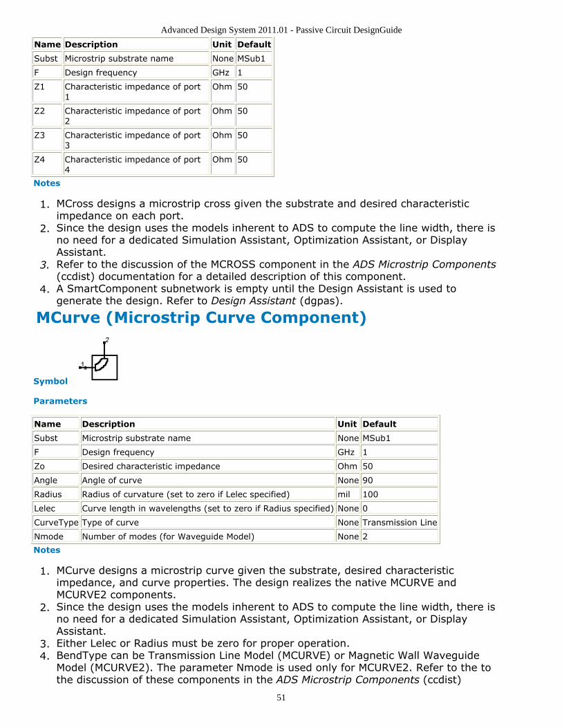
Advanced Design System 2011.01 - Passive Circuit DesignGuide
51
Name Description Unit Default
Subst Microstrip substrate name None MSub1
F Design frequency GHz 1
Z1 Characteristic impedance of port1
Ohm 50
Z2 Characteristic impedance of port2
Ohm 50
Z3 Characteristic impedance of port3
Ohm 50
Z4 Characteristic impedance of port4
Ohm 50
Notes
MCross designs a microstrip cross given the substrate and desired characteristic1.impedance on each port.Since the design uses the models inherent to ADS to compute the line width, there is2.no need for a dedicated Simulation Assistant, Optimization Assistant, or DisplayAssistant.Refer to the discussion of the MCROSS component in the ADS Microstrip Components3.(ccdist) documentation for a detailed description of this component.A SmartComponent subnetwork is empty until the Design Assistant is used to4.generate the design. Refer to Design Assistant (dgpas).
MCurve (Microstrip Curve Component)
Symbol
Parameters
Name Description Unit Default
Subst Microstrip substrate name None MSub1
F Design frequency GHz 1
Zo Desired characteristic impedance Ohm 50
Angle Angle of curve None 90
Radius Radius of curvature (set to zero if Lelec specified) mil 100
Lelec Curve length in wavelengths (set to zero if Radius specified) None 0
CurveType Type of curve None Transmission Line
Nmode Number of modes (for Waveguide Model) None 2
Notes
MCurve designs a microstrip curve given the substrate, desired characteristic1.impedance, and curve properties. The design realizes the native MCURVE andMCURVE2 components.Since the design uses the models inherent to ADS to compute the line width, there is2.no need for a dedicated Simulation Assistant, Optimization Assistant, or DisplayAssistant.Either Lelec or Radius must be zero for proper operation.3.BendType can be Transmission Line Model (MCURVE) or Magnetic Wall Waveguide4.Model (MCURVE2). The parameter Nmode is used only for MCURVE2. Refer to the tothe discussion of these components in the ADS Microstrip Components (ccdist)

Advanced Design System 2011.01 - Passive Circuit DesignGuide
52
documentation for a more detailed description.A SmartComponent subnetwork is empty until the Design Assistant is used to5.generate the design. Refer to Design Assistant (dgpas).
MGap (Microstrip Gap Component)
Symbol
Parameters
Name Description Unit Default
Subst Microstrip substrate name None MSub1
F Design frequency GHz 1
Zo Desired characteristic impedance Ohm 50
S Length of gap (spacing) mil 50
Notes
MGap designs a microstrip gap given the substrate, desired characteristic impedance,1.and gap width.Since the design uses the models inherent to ADS to compute the line width, there is2.no need for a dedicated Simulation Assistant, Optimization Assistant, or DisplayAssistant.Refer to the discussion of the MGAP component in the ADS Microstrip Components3.(ccdist) documentation for a detailed description of this component.A SmartComponent subnetwork is empty until the Design Assistant is used to4.generate the design. Refer to Design Assistant (dgpas).
MLine (Microstrip Line)
Symbol
Parameters
Name Description Unit Default
Subst Microstrip substrate name None MSub1
F Design frequency GHz 1
Zo Desired characteristic impedance Ohm 50
Lphys Physical line length; set to zero if Lelec specified mil 0
Lelec Line length in wavelengths; set to zero if Lphys specified None 0.25
Notes
MLine designs a microstrip line given the substrate, desired characteristic impedance,1.and physical or electrical length.Since the design uses the models inherent to ADS to compute the line width and2.length, there is no need for a dedicated Simulation Assistant, Optimization Assistant,or Display Assistant.For proper operation, either Lphys or Lelec must be zero.3.Refer to the discussion of the MLIN component in the ADS Microstrip Components4.(ccdist) documentation for a more detailed description of the model used for this
Advanced Design System 2011.01 - Passive Circuit DesignGuide
53
component.A SmartComponent subnetwork is empty until the Design Assistant is used to5.generate the design. Refer to Design Assistant (dgpas).
MMndr (Microstrip Meander Line)
Symbol
Parameters
Name Description Unit Default
Subst Microstrip substrate name None MSub1
F Design frequency GHz 1
Zo Desired characteristic impedance Ohm 50
Lphys Physical line length (set to zero if Lelec specified) mil 0
Lelec Line length in wavelengths (set to zero if Lphys specified) None 0.25
WR Bounding rectangle width mil 1000
HR Bounding rectangle height mil 1000
Delta Length added to vertical lines for tuning performance mil 0
Notes
MMndr designs a meandering microstrip line given the substrate, desired1.characteristic impedance, physical or electrical length, and maximum rectangulardimensions of the line.The line input and output ports are at the center of the rectangle on the side2.characterized by HR.The final width and height of the bounding box can be smaller than that specified3.depending on the desired length.For proper operation, either Lphys or Lelec must be zero.4.Refer to the discussion of the MLIN component in the ADS Microstrip Components5.(ccdist) documentation for a more detailed description of the model used for thiscomponent.The optimization minimizes the absolute difference between the transmission phase6.and that resulting from the specified length. Only the vertical dimension is optimized,and since the corners tend to add excess phase delay the resulting height will beslightly smaller than specified.A SmartComponent subnetwork is empty until the Design Assistant is used to7.generate the design. Refer to Design Assistant (dgpas).
Example
A MMndr component was used to design a 1-wavelength line in a 1-inch by 1-inch squarearea at a center frequency of 1 GHz. Optimization yielded a value of Delta = -10.469 mil.
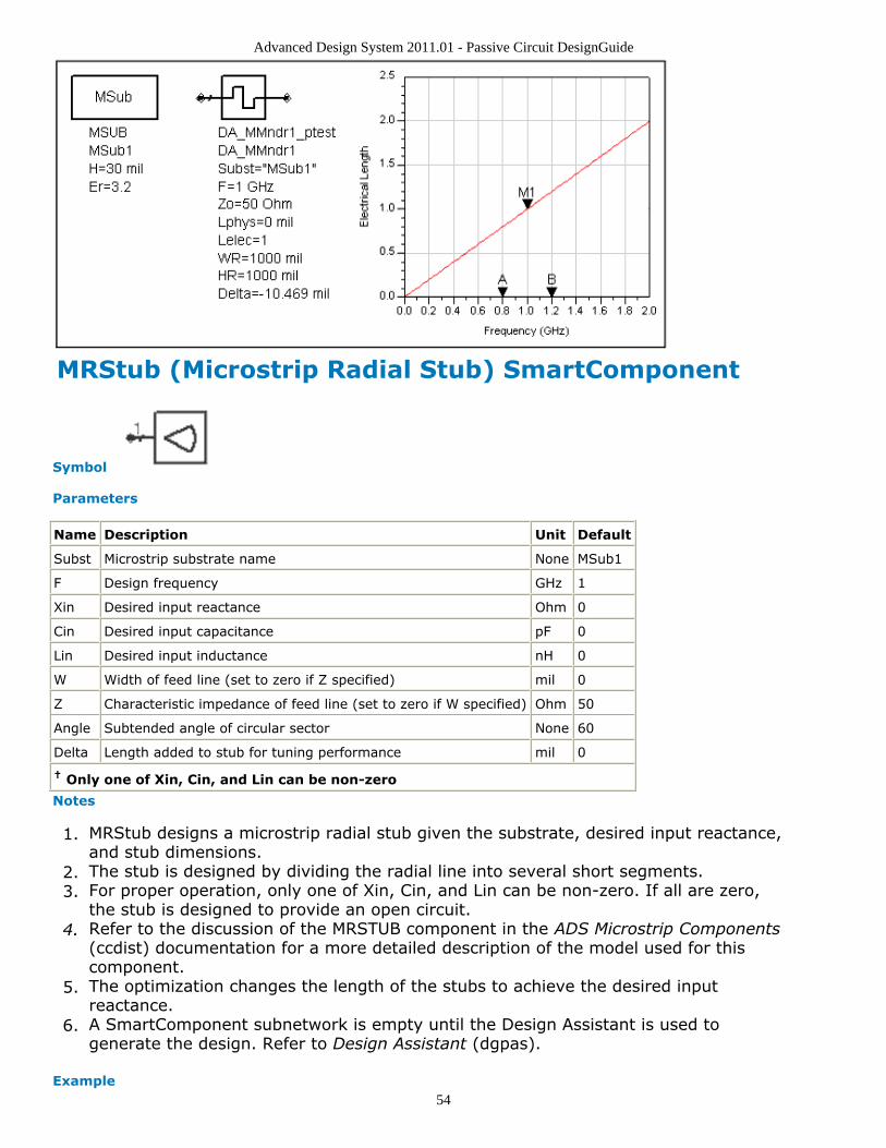
Advanced Design System 2011.01 - Passive Circuit DesignGuide
54
MRStub (Microstrip Radial Stub) SmartComponent
Symbol
Parameters
Name Description Unit Default
Subst Microstrip substrate name None MSub1
F Design frequency GHz 1
Xin Desired input reactance Ohm 0
Cin Desired input capacitance pF 0
Lin Desired input inductance nH 0
W Width of feed line (set to zero if Z specified) mil 0
Z Characteristic impedance of feed line (set to zero if W specified) Ohm 50
Angle Subtended angle of circular sector None 60
Delta Length added to stub for tuning performance mil 0
† Only one of Xin, Cin, and Lin can be non-zero
Notes
MRStub designs a microstrip radial stub given the substrate, desired input reactance,1.and stub dimensions.The stub is designed by dividing the radial line into several short segments.2.For proper operation, only one of Xin, Cin, and Lin can be non-zero. If all are zero,3.the stub is designed to provide an open circuit.Refer to the discussion of the MRSTUB component in the ADS Microstrip Components4.(ccdist) documentation for a more detailed description of the model used for thiscomponent.The optimization changes the length of the stubs to achieve the desired input5.reactance.A SmartComponent subnetwork is empty until the Design Assistant is used to6.generate the design. Refer to Design Assistant (dgpas).
Example

Advanced Design System 2011.01 - Passive Circuit DesignGuide
55
A MRStub component was used to design an open circuit stub at a center frequency of 1GHz. Optimization yielded a value of Delta = -40.092 mil.
MStep (Microstrip Step Component)
Symbol
Parameters
Name Description Unit Default
Subst Microstrip substrate name None MSub1
F Design frequency GHz 1
Z1 Characteristic impedance of port 1 Ohm 50
Z2 Characteristic impedance of port 2 Ohm 25
Notes
MStep designs a microstrip step given the substrate and desired characteristic1.impedances.Since the design uses the models inherent to ADS to compute the line width, there is2.no need for a dedicated Simulation Assistant, Optimization Assistant, or DisplayAssistant.Refer to the discussion of the MSTEP component in the ADS Microstrip Components3.(ccdist) documentation for a detailed description of this component.A SmartComponent subnetwork is empty until the Design Assistant is used to4.generate the design. Refer to Design Assistant (dgpas).
MStub (Microstrip Stub)
Symbol
Parameters
Advanced Design System 2011.01 - Passive Circuit DesignGuide
56
Name Description Unit Default
Subst Microstrip substrate name None MSub1
F Design frequency GHz 1
Zo Desired characteristic impedance Ohm 50
Lphys Physical line length mil 0
Lelec Line length in wavelengths None 0
Xin Desired input reactance Ohm 0
Cin Desired input capacitance pF 0
Lin Desired input inductance nH 0
StubType Type of stub None OpenCircuit
Notes
MStub designs a microstrip open or short circuited stub given the substrate, desired1.characteristic impedance, and physical or electrical length. The design realizes thenative MLOC, MLSC, and MLEF components.Only one of Lphys, Lelec, Xin, Cin, and Lin can be non-zero.2.Since the design uses the models inherent to ADS to compute the line width and3.length, there is no need for a dedicated Simulation Assistant, Optimization Assistant,or Display Assistant.For proper operation, only one of Lphys, Lelec, Xin, Cin, and Lin can be non-zero.4.StubType can be either Open Circuit (MLOC), End Effect (MLEF), or Short Circuit5.(MLSC). Refer to the discussion of these components in the ADS MicrostripComponents (ccdist) documentation for a more detailed description of these differentoptions.A SmartComponent subnetwork is empty until the Design Assistant is used to6.generate the design. Refer to Design Assistant (dgpas).
MTaper (Microstrip Taper Component)
Symbol
Parameters
Name Description Unit Default
Subst Microstrip substrate name None MSub1
F Design frequency GHz 1
Z1 Characteristic impedance at port 1 Ohm 50
Z2 Characteristic impedance at port 2 Ohm 25
Lphys Physical line length (set to zero if Lelec specified) mil 0
Lelec Line length in wavelengths (set to zero if Lphys specified) None 0.10
Notes
MTaper designs a microstrip tapered line given the substrate, desired characteristic1.impedance, and physical or electrical length.Since the design uses the models inherent to ADS to compute the line width and2.length, there is no need for a dedicated Simulation Assistant, Optimization Assistant,or Display Assistant.For proper operation, either Lphys or Lelec must be zero.3.Z1 and Z2 are used to determine the widths at each end of the taper component.4.

Advanced Design System 2011.01 - Passive Circuit DesignGuide
57
Refer to the discussion of the MTAPER component in the ADS Microstrip Components(ccdist) documentation for a more detailed description of this component.A SmartComponent subnetwork is empty until the Design Assistant is used to5.generate the design. Refer to Design Assistant (dgpas).
MTee (Microstrip Tee Component)
Symbol
Parameters
Name Description Unit Default
Subst Microstrip substrate name None MSub1
F Design frequency GHz 1
Z1 Characteristic impedance of port1
Ohm 50
Z2 Characteristic impedance of port2
Ohm 50
Z3 Characteristic impedance of port3
Ohm 50
Notes
MTee designs a microstrip tee given the substrate and desired characteristic1.impedance at each port.Since the design uses the models inherent to ADS to compute the line width and2.length, there is no need for a dedicated Simulation Assistant, Optimization Assistant,or Display Assistant.Z1, Z2, and Z3 are used to determine the widths of each port. Refer to the discussion3.of the MTEE component in the ADS Microstrip Components (ccdist) documentation fora more detailed description of this component.A SmartComponent subnetwork is empty until the Design Assistant is used to4.generate the design. Refer to Design Assistant (dgpas).
Passive Microstrip CircuitsBLCoupler (Branch-Line Coupler) (dgpas)CLCoupler (Coupled-Line Coupler) (dgpas)CLFilter (Coupled-Line Filter) (dgpas)CMFilter (Comb-Line Filter) (dgpas)DSMatch (Double-Stub Match) (dgpas)HPFilter (Hairpin Filter) (dgpas)IDFilter (Interdigital Filter) (dgpas)LCoupler (Lange Coupler) (dgpas)LEMatch (Lumped Component Match) (dgpas)QWMatch (Quarter-Wave Match) (dgpas)RAtten (Resistive Attenuator) (dgpas)RRCoupler (Rat-Race Coupler) (dgpas)SBFilter (Stub Bandpass Filter) (dgpas)SIFilter (Stepped Impedance Lowpass Filter) (dgpas)SLFilter (Stub Lowpass Filter) (dgpas)SRFilter (Stepped Impedance Resonator Filter) (dgpas)SSMatch (Single-Stub Match) (dgpas)TCoupler (Tee Power Divider) (dgpas)

Advanced Design System 2011.01 - Passive Circuit DesignGuide
58
TLMatch (Tapered-Line Match) (dgpas)WDCoupler (Wilkinson Divider) (dgpas)ZZFilter (Zig-Zag Coupled-Line Filter) (dgpas)
NoteA SmartComponent subnetwork is empty until the Design Assistant is used to generate the design. Referto Design Assistant (dgpas).
BLCoupler (Branch-Line Coupler)
Symbol
Parameters
Name Description Unit Default
Subst Microstrip substrate name None MSub1
F Center frequency GHz 1
DeltaF Total frequency bandwidth GHz 0.5
Zo Characteristic impedance Ohm 50
ResponseType Type of frequency response None Chebyshev
N Number of coupler sections; set N=0 to computeN
None 0
Rmax Maximum voltage reflection coefficient at the input None 0.5
C Coupling coefficient dB 3
Delta Length added to branches for tuning performance mil 0
Notes
A branch-line coupler outputs from the coupled port (pin 3) a fraction of the power1.presented at the input (pin 1). The remainder of the power is passed through to theoutput port (pin 2). At the center frequency the phase difference between theoutputs is 90 degrees, with the coupled port representing the quadrature (Q) outputand the output port representing the in-phase (I) output. The coupling coefficientspecifies the ratio of the input power to the coupled power (P1/P3). Pin 4 represents
the isolated port, and it is typically well isolated from the input port near the centerfrequency.The coupling coefficient must be positive and greater than 3 dB. Best results are2.obtained for tight couplings of 6 dB or better (C < 6 dB). Choosing the couplingparameter larger than 6 dB often causes width constraint violations to occur on theMTEE components, resulting in warning messages during design and simulation. Acoupling coefficient of 3 dB provides an equal power split between the two outputs.For broadband performance, the coupler can have multiple sections. If the number of3.sections N is set to zero, the Design Assistant chooses N such that the reflectioncoefficient is less than Rmax over the bandwidth DeltaF (centered at the designcenter frequency). The resulting bandwidth can be broader than that specified.Otherwise, rmax and DeltaF are ignored.The ResponseType specifies the distribution of the partial reflection coefficients seen4.at each section interface - Uniform, Binomial, and Chebyshev distributions areavailable.The optimization minimizes the input reflection coefficient (S11) at the design center5.frequency by changing the length of the lines forming the four branches. All branches

Advanced Design System 2011.01 - Passive Circuit DesignGuide
59
are changed by the same physical length during the optimization.This optimizationgenerally provides very good results but can not guarantee that the specifiedcoupling is attained at the design frequency. More advanced tuning can be performedby changing line width of the branch lines.A SmartComponent subnetwork is empty until the Design Assistant is used to6.generate the design. Refer to Design Assistant (dgpas).
For a more detailed discussion of this device, see: D. M. Pozar, Microwave Engineering,2nd Edition, John Wiley & Sons: New York, 1998, pp. 379-383.
Example
A single-section branch-line coupler was designed for a center frequency of 5 GHz with anequal power split between the I and Q ports. Tuning using the Optimization Assistantyielded a value of Delta = 49.532 mil.
CLCoupler (Coupled-Line Coupler)
Symbol
Parameters
Name Description Unit Default
Subst Microstrip substrate name None MSub1
F Center frequency GHz 1
C Coupling coefficient dB 20
Zo Characteristic impedance Ohm 50
N Number of coupler sections (N is odd) None 1
Delta Length added to branches for tuningperformance
mil 0
Notes
A coupled-line coupler outputs from the coupled port (pin 4) a fraction of the power1.
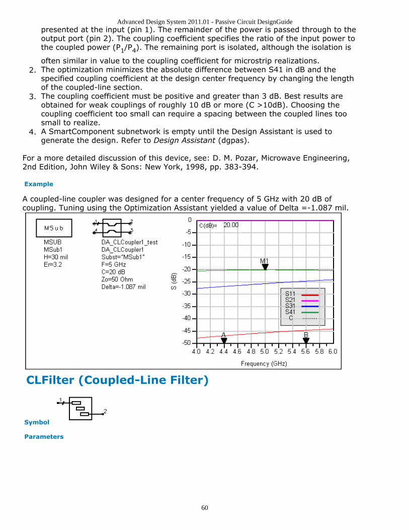
Advanced Design System 2011.01 - Passive Circuit DesignGuide
60
presented at the input (pin 1). The remainder of the power is passed through to theoutput port (pin 2). The coupling coefficient specifies the ratio of the input power tothe coupled power (P1/P4). The remaining port is isolated, although the isolation is
often similar in value to the coupling coefficient for microstrip realizations.The optimization minimizes the absolute difference between S41 in dB and the2.specified coupling coefficient at the design center frequency by changing the lengthof the coupled-line section.The coupling coefficient must be positive and greater than 3 dB. Best results are3.obtained for weak couplings of roughly 10 dB or more (C >10dB). Choosing thecoupling coefficient too small can require a spacing between the coupled lines toosmall to realize.A SmartComponent subnetwork is empty until the Design Assistant is used to4.generate the design. Refer to Design Assistant (dgpas).
For a more detailed discussion of this device, see: D. M. Pozar, Microwave Engineering,2nd Edition, John Wiley & Sons: New York, 1998, pp. 383-394.
Example
A coupled-line coupler was designed for a center frequency of 5 GHz with 20 dB ofcoupling. Tuning using the Optimization Assistant yielded a value of Delta =-1.087 mil.
CLFilter (Coupled-Line Filter)
Symbol
Parameters
Advanced Design System 2011.01 - Passive Circuit DesignGuide
61
Name Description Unit Default
Subst Microstrip substrate name None MSub1
Fs1 Lower stopband edge frequency GHz 1.8
Fp1 lower passband edge frequency GHz 2
Fp2 upper passband edge frequency GHz 2.2
Fs2 lower stopband edge frequency GHz 2.4
Ap passband edge attenuation (or ripple for Chebyshev) dB 3
As stopband edge attenuation dB 20
N number of filter sections (or 0 to compute N) None 0
ResponseType type of frequency response (maximally flat orChebyshev)
None Maximally Flat
Zo desired input/output impedance Ohm 50
CouplingType Type of input/output coupling None Coupled Line TransformerInput
Delta length added to coupled sections for tuning performance mil 0
Notes
A coupled-line filter provides a bandpass frequency response between the input and1.output ports. N coupled-line sections produces an N-1 order filter response.Additional numbers of sections can be used to steepen the transition band roll off orwiden the pass bandwidth.Because of the heavy computational burden in determining the line parameters, a2.brief delay will occur for the design.For a Chebyshev (equal ripple) frequency response, ripple levels greater than about 13.dB are not recommended. Exceeding this value will typically deform the shape of thepassband characteristics.If N is zero, the number of filter sections will be computed from the4.frequency/attenuation information. If N is non-zero, the design will use thefrequency/attenuation parameters only for determining the design center frequency.Using a Coupled Line Transformer Input CouplingType will use and extra coupled line5.section on the inputs and outputs to feed the device. Choosing Tapped LineTransformer Input will bring the feedline directly into the first resonator.The optimization minimizes the absolute difference between S21 in dB and the6.specified passband edge attenuation (which equals the ripple for Chebyshevresponse) at the passband edge frequencies. Because only the line lengths arechanged, this tuning will typically center the response within the specified passband.More advanced shaping of the passband response can be accomplished by manuallytuning the widths and spacings of the coupled filter sections.A SmartComponent subnetwork is empty until the Design Assistant is used to7.generate the design. Refer to Design Assistant (dgpas).
For a more detailed discussion of this device, see D. M. Pozar, Microwave Engineering, 2ndEdition, John Wiley & Sons: New York, 1998, pp. 477-485.
Example
A coupled-line filter was designed for a maximally flat response with the 3 dB passbandedge frequencies at 2 GHz and 2.4 GHz respectively. Coupled Line Transformer Inputswere used. The design required 4 coupled-line sections. Tuning using the OptimizationAssistant yielded a value of Delta = -5.244 mil.

Advanced Design System 2011.01 - Passive Circuit DesignGuide
62
CMFilter (Comb-Line Filter)
Symbol
Parameters
Name Description Unit Default
Subst microstrip substrate name None Subst1
Fs1 lower stopband edge frequency GHz 1.8
Fp1 lower passband edge frequency GHz 2
Fp2 upper passband edge frequency GHz 2.2
Fs2 lower stopband edge frequency GHz 2.4
Ap passband edge attenuation (or ripple for Chebyshev) dB 3
As stopband edge attenuation dB 20
N number of filter sections (or 0 to compute N) None 0
ResponseType type of frequency response (maximally flat or Chebyshev) None Maximally Flat
Zo desired input/output impedance Ohm 50
Lelec electrical length of filter resonators (the units of Leclec are infractions of a wavelength i.e., 0.25=1/4 wavelength)
None 0.05
ya normalized interior resonator admittance (0 < ya < 1) None 0.7
CouplingType type of input/output coupling (coupled line or tapped linetransformer)
None Tapped LineTransformer Input
Delta length added to coupled sections for tuning performance mil 0
Notes
A comb-line filter provides a bandpass frequency response between the input and1.output ports. N coupled-line sections produce an N-1 order filter response. Additionalnumbers of sections can be used to steepen the transition band roll off or widen thepass bandwidth.Because of the heavy computational burden in determining the line parameters, a2.brief delay will occur for the design.A two-layer substrate must be used for this topology.3.

Advanced Design System 2011.01 - Passive Circuit DesignGuide
63
For a Chebyshev (equal ripple) frequency response, ripple levels greater than about 14.dB are not recommended. Exceeding this value will typically deform the shape of thepassband characteristics.If N is zero, the number of filter sections will be computed from the5.frequency/attenuation information. If N is non-zero, the design will use thefrequency/attenuation parameters only for determining the design center frequency.Using a CouplingType of "Coupled Line Transformer Input" will use an extra coupled6.line section on the inputs and outputs to feed the device. Choosing "Tapped LineTransformer Input" will bring the feedline directly into the first resonator.The optimization minimizes the absolute difference between S21 in dB and the7.specified passband edge attenuation (which equals the ripple for Chebyshevresponse) at the passband edge frequencies. Because only the line lengths arechanged, this tuning will typically center the response within the specified passband.More advanced shaping of the passband response can be accomplished by manuallytuning the widths and spacings of the coupled filter sections.A SmartComponent subnetwork is empty until the Design Assistant is used to8.generate the design. Refer to Design Assistant (dgpas).
For a more detailed discussion of this device, refer to: Matthaei, Young and Jones,Microwave Filters, Impedance-Matching Networks, and Coupling Structures, Artech House,1980, pp. 497.
Example
A comb-line filter was designed for a maximally flat response with the 3 dB passband edgefrequencies at 2 GHz and 2.2 GHz respectively. The design required 5coupled lines. Tuningusing the Optimization Assistant yielded a value of Delta = 168.41 mil.
DSMatch (Double-Stub Match)
Symbol
Parameters

Advanced Design System 2011.01 - Passive Circuit DesignGuide
64
Name Description Unit Default
Subst Microstrip substrate name None MSub1
F Center frequency GHz 1
Zin Desired complex input impedance Ohm 50
Zload Complex load impedance to match Ohm 100
Zstub1 Characteristic impedance of stub line 1 (nearest input) Ohm 50
Zstub2 Characteristic impedance of stub line 2 (nearest output) Ohm 50
Zline Characteristic impedance of line between stubs Ohm 50
Zfeed1 Characteristic impedance of line connected to port 1 Ohm 50
Zfeed2 Characteristic impedance of line connected to port 2 Ohm 50
Stub1Type Stub 1 type (open or short circuit) None OpenCircuit
Stub2Type Stub 2 type (open or short circuit) None OpenCircuit
Delta Length added to stubs for tuning performance mil 0
Notes
A double-stub matching network matches a complex load impedance (Zload) to a1.desired complex input impedance (Zin) using two shunt stubs and a connecting line.An impedance match can be realized using any combination of stub types, although2.some combinations can be more realizable.Zfeed1 and Zfeed2 are used simply to ensure that the input and output legs of the3.microstrip tee components are of the proper width.The length of the line between the stubs is nominally chosen to be an eighth of a line4.wavelength. However, if this will not realize the match, the length of line is computedsuch that the rotated circle on the Smith chart encloses the load admittance.MTEE component width constraint violations will be avoided generally by choosing5.similar characteristic impedances for the line, stub, and feed.Since two solutions are possible, the solution that results in the smallest length of6.stub 1 is chosen. For example, if stub 1 is open circuited, the solution for which stub1 must realize a capacitive reactance is chosen.The input port termination is set to the conjugate of Zin so that the ideal input7.reflection coefficient will be zero. The output port termination is set to Zload.The optimization minimizes the value of S11 (referenced to the conjugate of Zin) at8.the design center frequency by changing the length of the stubs. Both stubs aretuned by the same length.A SmartComponent subnetwork is empty until the Design Assistant is used to9.generate the design. Refer to Design Assistant (dgpas).
For a more detailed discussion of this device, see: D. M. Pozar, Microwave Engineering,2nd Edition, John Wiley & Sons: New York, 1998, pp. 266-271.
Example
A double-stub matching network was designed to match a load impedance of 100 - j30Ohms to a 50 Ohm line at a center frequency of 5 GHz with open circuited stubs. Tuningusing the Optimization Assistant yielded a value of Delta = -31.633 mil.

Advanced Design System 2011.01 - Passive Circuit DesignGuide
65
HPFilter (Hairpin Filter)
Symbol
Parameters
Name Description Unit Default
Subst Microstrip substrate name None MSub1
Fs1 Lower stopband edge frequency GHz 1.8
Fp1 Lower passband edge frequency GHz 2
Fp2 Upper passband edge frequency GHz 2.2
Fs2 Lower stopband edge frequency GHz 2.4
Ap Passband edge attenuation (or ripple for Chebyshev) dB 3
As Stopband edge attenuation dB 20
N Number of filter sections (or 0 to compute N) None 0
ResponseType Type of frequency response (maximally flat or Chebyshev) None Maximally Flat
Zo Desired input/output impedance Ohm 50
Sphys Physical spacing between legs within hairpin resonator; set tozero if Selec specified
mil 0
Selec Spacing between legs within hairpin resonator in wavelengths;set to zero if Sphys specified
None 0.25
CouplingType Type of input/output coupling (coupled line or tapped linetransformer)
None Coupled LineTransmission Input
Delta Length added to coupled sections for tuning performance mil 0
Notes
A hairpin filter provides a bandpass frequency response between the input and output1.ports. N coupled-line sections produce an N-1 order filter response. Additionalnumbers of sections can be used to steepen the transition band roll off or widen thepass bandwidth.Because of the heavy computational burden in determining the line parameters, a2.brief delay will occur for the design.

Advanced Design System 2011.01 - Passive Circuit DesignGuide
66
For a Chebyshev (equal ripple) frequency response, ripple levels greater than about 13.dB are not recommended. Exceeding this value will typically deform the shape of thepassband characteristics.If N is zero, the number of filter sections will be computed from the4.frequency/attenuation information. If N is non-zero, the design will use thefrequency/attenuation parameters only for determining the design center frequency.Using a Coupled Line Transformer Input CouplingType will use and extra coupled line5.section on the inputs and outputs to feed the device. Choosing Tapped LineTransformer Input will bring the feedline directly into the first resonator.The optimization minimizes the absolute difference between S21 in dB and the6.specified passband edge attenuation (which equals the ripple for Chebyshevresponse) at the passband edge frequencies. Because only the line lengths arechanged, this tuning will typically center the response within the specified passband.More advanced shaping of the passband response can be accomplished by manuallytuning the widths and spacings of the coupled filter sections.A SmartComponent subnetwork is empty until the Design Assistant is used to7.generate the design. Refer to Design Assistant (dgpas).
For a more detailed discussion of this device, refer to: Cristal and Frankel, "Hairpin-lineand hybrid hairpin-line/half-wave parallel-coupled-line filters," IEEE Trans. MicrowaveTheory and Techniques, vol MTT-20, pp. 719-728, 1972.
Example
A hairpin filter was designed for a maximally flat response with the 3 dB passband edgefrequencies at 2 GHz and 2.2 GHz respectively. Coupled line transformer inputs wereused. The design required 4 coupled sections. Tuning using the Optimization Assistantyielded a value of Delta = -41.682 mil.
IDFilter (Interdigital Filter)
Symbol
Parameters

Advanced Design System 2011.01 - Passive Circuit DesignGuide
67
Name Description Unit Default
Subst Microstrip substrate name None Subst1
Fs1 Lower stopband edge frequency GHz 1.8
Fp1 Lower passband edge frequency GHz 2
Fp2 Upper passband edge frequency GHz 2.2
Fs2 Lower stopband edge frequency GHz 2.4
Ap Passband edge attenuation (or ripple for Chebyshev) dB 3
As Stopband edge attenuation dB 20
N Number of filter sections (or 0 to compute N) None 0
ResponseType Type of frequency response (Maximally Flat or Chebyshev) None Maximally Flat
Zo Desired input/output impedance Ohm 50
ya Normalized interior resonator admittance (0 < ya < 1) None 1
CouplingType Type of input/output coupling (coupled line or tapped linetransformer)
None Coupled Line TransformerInput
Delta Length added to coupled sections for tuning performance mil 0
Notes
An interdigital filter provides a bandpass frequency response between the input and1.output ports. N coupled-line sections produce an N-1 order filter response. Additionalnumbers of sections can be used to steepen the transition band roll off or widen thepass bandwidth.Because of the heavy computational burden in determining the line parameters, a2.brief delay will occur for the design.A two-layer substrate must be used for this topology.3.For a Chebyshev (equal ripple) frequency response, ripple levels greater than about 14.dB are not recommended. Exceeding this value will typically deform the shape of thepassband characteristics.If N is zero, the number of filter sections will be computed from the5.frequency/attenuation information. If N is non-zero, the design will use thefrequency/attenuation parameters only for determining the design center frequency.Using a CouplingType of "Coupled Line Transformer Input" will use an extra coupled6.line section on the inputs and outputs to feed the device. Choosing "Tapped LineTransformer Input" will bring the feedline directly into the first resonator.The optimization minimizes the absolute difference between S21 in dB and the7.specified passband edge attenuation (which equals the ripple for Chebyshevresponse) at the passband edge frequencies. Because only the line lengths arechanged, this tuning will typically center the response within the specified passband.More advanced shaping of the passband response can be accomplished by manuallytuning the widths and spacings of the coupled filter sections.A SmartComponent subnetwork is empty until the Design Assistant is used to8.generate the design. Refer to Design Assistant (dgpas).
For a more detailed discussion of this device, refer to: Matthaei, Young and Jones,Microwave Filters, Impedance-Matching Networks, and Coupling Structures, Artech House,1980, pp. 614.
Example
An interdigital filter was designed for a maximally flat response with the 3 dB passbandedge frequencies at 2 GHz and 2.2 GHz respectively. The design required 5coupled lines.Tuning using the Optimization Assistant yielded a value of Delta = 14.979 mil.

Advanced Design System 2011.01 - Passive Circuit DesignGuide
68
LCoupler (Lange Coupler)
Symbol
Parameters
Name Description Unit Default
Subst Microstrip substrate name None MSub1
F Center frequency GHz 1
C Coupling coefficient dB 20
N Number of fingers (4, 6, or 8) None 4
Zo Characteristic impedance Ohm 50
Delta Length added to fingers for tuning performance mil 0
Notes
A Lange coupler outputs from pin 2 a small fraction of the power presented at the1.input (pin 1). The remainder of the power is passed through pin 3. The couplingcoefficient specifies the power ratio P1/P2. Pin 4 is isolated, and often the isolation is
10 dB better than the coupling coefficient in microstrip realizations.The Lange coupler is best for weak couplings of roughly 10 dB or more (C >10dB).2.Choosing the coupling coefficient too small can produce an unrealizable design. If thedesign creates a finger spacing S that is not realizable, increase the value of N.The Design Assistant computes the required even and odd mode impedances to3.achieve the desired coupling and translates them to finger width and spacing. Thelength of the fingers is a quarter wavelength at the design frequency.The optimization minimizes the absolute difference between S21 and the specified4.coupling coefficient at the design center frequency by changing the length of thefingers section.A SmartComponent subnetwork is empty until the Design Assistant is used to5.generate the design. Refer to Design Assistant (dgpas).
For a more detailed discussion of this device, see: I. Bahl and P. Bhartia, Microwave SolidState Circuit Design, John Wiley & Sons: New York, 1988, pp. 209-211.

Advanced Design System 2011.01 - Passive Circuit DesignGuide
69
Example
A Lange coupler was designed for a center frequency of 3 GHz with 20 dB of coupling and6 fingers. Tuning using the Optimization Assistant yielded a value of Delta = -4.57 mil.
LEMatch (Lumped Component Match)
Symbol
Parameters
Name Description Unit Default
F Center frequency GHz 1
Zin Desired complex input impedance Ohm 50
Zload Complex load impedance to match Ohm 100
NetworkType Type of network (source to load) None AllowSelection
Notes
A lumped component matching network uses reactive components to match a1.complex load impedance (Zload) to a desired complex input impedance (Zin).The network type specifies the type of reactive components used (L represents2.inductance, C represents capacitance) as well as their orientation (series or shunt).The first component specified is that nearest the source, while the second is thatnearest the load. If the chosen network type cannot realize the impedance matchspecified, or if the network type is chosen as "Allow Selection", a dialog box willappear allowing selection from the possible network types that can perform thematch.Either two or four distinct networks are possible depending on the load and input3.impedance specified.The input port termination is set to the conjugate of Zin so that the ideal input4.reflection coefficient will be zero. The output port termination is set to Zload.No optimization assistant is provided since the design procedure is exact for ideal5.lumped component models.A SmartComponent subnetwork is empty until the Design Assistant is used to6.

Advanced Design System 2011.01 - Passive Circuit DesignGuide
70
generate the design. Refer to Design Assistant (dgpas).
For a more detailed discussion of this device, see: D. M. Pozar, Microwave Engineering,2nd Edition, John Wiley & Sons: New York, 1998, pp. 252-258.
Example
A lumped component matching network was designed to match a load impedance of 100 -j30 Ohms to an input impedance of 50 Ohms at a center frequency of 1 GHz. A Series LShunt C configuration was used to realize this match.
QWMatch (Quarter-Wave Match)
Symbol
Parameters
Name Description Unit Default
Subst Microstrip substrate name None MSub1
F Center frequency GHz 1
DeltaF Total frequency bandwidth GHz 0.5
Zo Desired input impedance Ohm 50
Rload Load impedance to match Ohm 100
ResponseType Type of frequency response None Uniform
N Number of quarter-wave sections; set N=0 to compute N None 0
Rmax Maximum voltage reflection coefficient None 0.1
Delta Length added to transformer sections for tuning performance mil 0
Notes
A quarter-wave matching network matches a real load impedance (Rload) to a1.desired real input impedance (Zo) using multiple quarter wavelength sections. Aspecified frequency response can be realized by proper design of the individualsections.DeltaF is defined as the total bandwidth centered at the design center frequency.2.

Advanced Design System 2011.01 - Passive Circuit DesignGuide
71
If the number of sections N is set to zero, the Design Assistant chooses N such that3.the reflection coefficient is less that Rmax over the bandwidth DeltaF. The resultingbandwidth may be broader than that specified. Otherwise, Rmax and DeltaF areignored.The ResponseType specifies the distribution of the partial reflection coefficients seen4.at each section interface - Uniform, Binomial, and Chebyshev distributions areavailable. These in turn specify the shape of the reflection coefficient versusfrequency.A single-section quarter-wave matching transformer can be designed by setting N =5.1.Since the reflection coefficient may not be at its minimum value at the design center6.frequency, the optimization centers the variation of S11 (referenced to the value ofZo) versus frequency at the center frequency by changing the length of each quarter-wave section. All sections are tuned by the same length during the optimization.A SmartComponent subnetwork is empty until the Design Assistant is used to7.generate the design. Refer to Design Assistant (dgpas).
For a more detailed discussion of this device, see: D. M. Pozar, Microwave Engineering,2nd Edition, John Wiley & Sons: New York, 1998, pp. 275-288; R. S. Elliott, AnIntroduction to Guided Waves and Microwave Circuits, Prentice Hall, John Wiley, NewJersey, 1993, pp. 218-224.
Example
A quarter-wave matching network was designed to match a load impedance of 100 Ohmsto a 50 Ohm line at a center frequency of 4 GHz. Specifying a Chebyshev frequencyresponse for which the reflection coefficient remains below 0.1 over a 3 GHz bandwidthdictates 3 quarter-wave sections. Tuning using the Optimization Assistant yielded a valueof Delta = -2.284 mil.
RAtten (Resistive Attenuator)
Symbol
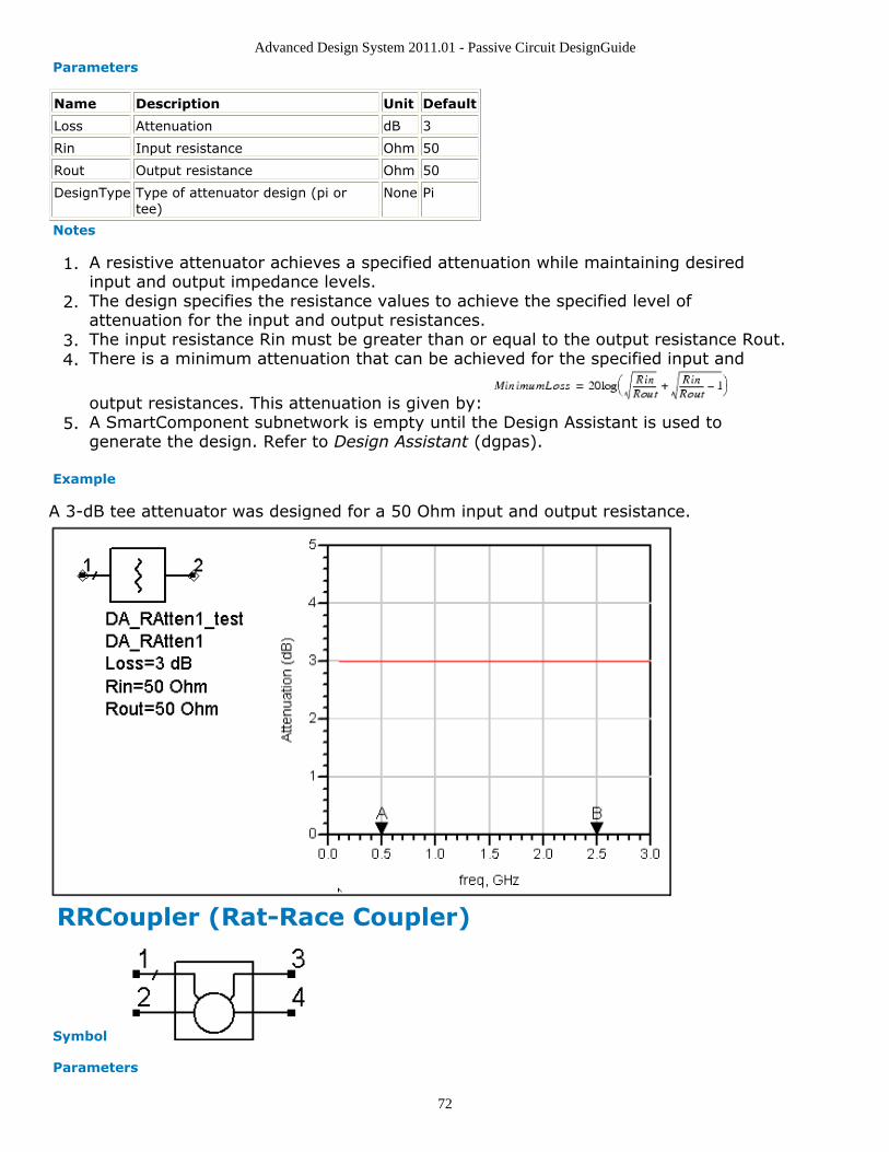
Advanced Design System 2011.01 - Passive Circuit DesignGuide
72
Parameters
Name Description Unit Default
Loss Attenuation dB 3
Rin Input resistance Ohm 50
Rout Output resistance Ohm 50
DesignType Type of attenuator design (pi ortee)
None Pi
Notes
A resistive attenuator achieves a specified attenuation while maintaining desired1.input and output impedance levels.The design specifies the resistance values to achieve the specified level of2.attenuation for the input and output resistances.The input resistance Rin must be greater than or equal to the output resistance Rout.3.There is a minimum attenuation that can be achieved for the specified input and4.
output resistances. This attenuation is given by: A SmartComponent subnetwork is empty until the Design Assistant is used to5.generate the design. Refer to Design Assistant (dgpas).
Example
A 3-dB tee attenuator was designed for a 50 Ohm input and output resistance.
RRCoupler (Rat-Race Coupler)
Symbol
Parameters

Advanced Design System 2011.01 - Passive Circuit DesignGuide
73
Name Description Unit Default
Subst Microstrip substrate name None MSub1
F Center frequency GHz 1
Zo Characteristic impedance Ohm 50
Delta Length added to ring branches fortuning
mil 0
Notes
A rat-race coupler equally divides the power input at port 1 between ports 2 and 3.1.The signal at the output ports 2 and 3 are in-phase. Port 4 is isolated from port 1. Ifthe signal is driven from port 2, then the power is divided between ports 1 and 4 withport 3 isolated. The signal at ports 1 and 4 are 180 degrees out of phase, andtherefore this device is sometimes referred to as a 180-degree hybrid.The design specifies the width and length of the microstrip lines to ensure that the2.ports are matched to Zo and equal power split is achieved at the design centerfrequency.The optimization minimizes the value of S11 (referenced to the value of Zo) at the3.design center frequency by changing the length of the ring.A SmartComponent subnetwork is empty until the Design Assistant is used to4.generate the design. Refer to Design Assistant (dgpas).
For a more detailed discussion of this device, see: D. M. Pozar, Microwave Engineering,2nd Edition, John Wiley & Sons: New York, 1998, pp. 401-407.
Example
A rat-race coupler was designed for a 50 Ohm system impedance at a center frequency of2 GHz. Tuning using the Optimization Assistant yielded a value of Delta = -2.099 mil.
SBFilter (Stub Bandpass Filter)
Symbol
Parameters
Advanced Design System 2011.01 - Passive Circuit DesignGuide
74
Name Description Unit Default
Subst Microstrip substrate name None MSub1
Fs1 Lower stopband edge frequency GHz 0.5
Fp1 Lower passband edge frequency GHz 1.3
Fp2 Upper passband edge frequency GHz 2.7
Fs2 Lower stopband edge frequency GHz 3.5
Ap Passband edge attenuation (or ripple for Chebyshev) dB 0.1
As Stopband edge attenuation dB 20
N Number of filter sections (or 0 to compute N) None 0
ResponseType Type of frequency response (maximally flat or Chebyshev) None Chebyshev
StubConfig Configuration of interior shunt stubs None Two Parallel Stubs
StubType Shunt Stub Type None Short Circuit Quarter Wave
Zo Desired input/output impedance Ohm 50
D Impedance control parameter (0 < D < 1) None 1
Finf Frequency of infinite attenuation (for open circuit stubtype)
GHz 1.0
Delta Length added to stubs for tuning performance mil 0
Notes
A stub bandpass filter provides a bandpass frequency response between the input1.and output ports. The design uses shunt stubs connected by lengths of transmissionline. If the specified passband response is too narrow, large differences in impedancevalues can result in a non-realizable configuration.This design is typically practical for fractional bandwidths of 0.4 to 0.7 or higher. If2.the bandwidth is too narrow, the design will generally require large differences inimpedances between the stubs and the connecting lines, producing an unrealizableconfiguration.For a Chebyshev (equal ripple) frequency response, ripple levels greater than about 13.dB are not recommended. Exceeding this value will typically deform the shape of thepassband characteristics.The parameter StubConfig specifies whether the interior stubs (all but those closest4.to the source and load) are implemented as a single stub or as two stubs in parallel.Choosing a single stub often produces narrower stub line widths, and therefore thisparameter can impact the ability to manufacture.The parameter D offers some control over the ratio between the stub impedances at5.the ends of the filter to those in the interior. In some cases where a MCROSS orMTEE width constraint violation is encountered, decreasing (or increasing) this valuein the range 0 < D < 1 can remedy the problem.If N is zero, the number of filter sections will be computed from the6.frequency/attenuation information. If N is non-zero, the design will use thefrequency/attenuation parameters only for determining the design center frequency.The optimization minimizes the absolute difference between S21 and the specified7.passband edge attenuation (which equals the ripple for Chebyshev response) at thepassband edge frequencies. All stub lengths are tuned by the same amount. Becauseonly the stub lengths are changed, this tuning will typically center the responsewithin the specified passband. More advanced shaping of the passband response canbe accomplished by manually tuning the widths and lengths of all lines.A SmartComponent subnetwork is empty until the Design Assistant is used to8.generate the design. Refer to Design Assistant (dgpas).
For a more detailed discussion of this device, see: Matthaei, Young and Jones, Microwave

Advanced Design System 2011.01 - Passive Circuit DesignGuide
75
Filters, Impedance-Matching Networks, and Coupling Structures, Artech House, 1980, pp.595-608.
Example
A stub bandpass filter was designed for a Chebyshev response with a 0.1 dB ripple. Thepassband edge frequencies are at 1.3GHz and 2.7 GHz respectively. The design uses twoparallel stubs in the interior regions with D = 1. The design required 4 stubs. Tuning usingthe Optimization Assistant yielded a value of Delta = -19.316 mil.
SIFilter (Stepped Impedance Lowpass Filter)
Symbol
Parameters
Name Description Unit Default
Subst Microstrip substrate name None MSub1
Fp Frequency at passband edge GHz 1
Ap Passband edge attenuation (or ripple for Chebyshev) dB 3
Fs Frequency at stopband edge GHz 1.2
As Stopband edge attenuation dB 20
N Number of filter sections (or 0 to compute N) None 0
ResponseType Type of frequency response (maximally flat orChebyshev)
None MaximallyFlat
FElement First filter component (automatic, capacitive, or inductive) None Automatic
Zo Desired input/output impedance Ohm 50
ZL Characteristic impedance of low impedance sections Ohm 25
ZH Characteristic impedance of high impedance sections Ohm 100
Delta Length added to filter sections for tuning performance mil 0
Notes
A stepped impedance filter provides a lowpass frequency response between the input1.
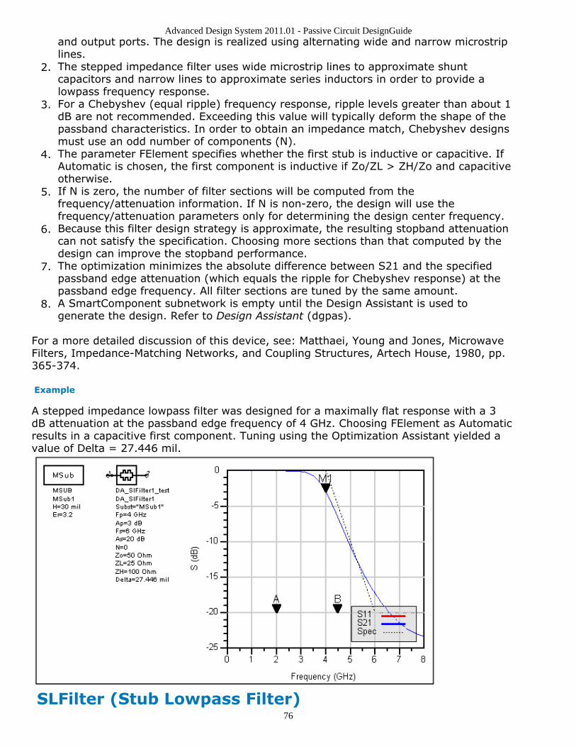
Advanced Design System 2011.01 - Passive Circuit DesignGuide
76
and output ports. The design is realized using alternating wide and narrow microstriplines.The stepped impedance filter uses wide microstrip lines to approximate shunt2.capacitors and narrow lines to approximate series inductors in order to provide alowpass frequency response.For a Chebyshev (equal ripple) frequency response, ripple levels greater than about 13.dB are not recommended. Exceeding this value will typically deform the shape of thepassband characteristics. In order to obtain an impedance match, Chebyshev designsmust use an odd number of components (N).The parameter FElement specifies whether the first stub is inductive or capacitive. If4.Automatic is chosen, the first component is inductive if Zo/ZL > ZH/Zo and capacitiveotherwise.If N is zero, the number of filter sections will be computed from the5.frequency/attenuation information. If N is non-zero, the design will use thefrequency/attenuation parameters only for determining the design center frequency.Because this filter design strategy is approximate, the resulting stopband attenuation6.can not satisfy the specification. Choosing more sections than that computed by thedesign can improve the stopband performance.The optimization minimizes the absolute difference between S21 and the specified7.passband edge attenuation (which equals the ripple for Chebyshev response) at thepassband edge frequency. All filter sections are tuned by the same amount.A SmartComponent subnetwork is empty until the Design Assistant is used to8.generate the design. Refer to Design Assistant (dgpas).
For a more detailed discussion of this device, see: Matthaei, Young and Jones, MicrowaveFilters, Impedance-Matching Networks, and Coupling Structures, Artech House, 1980, pp.365-374.
Example
A stepped impedance lowpass filter was designed for a maximally flat response with a 3dB attenuation at the passband edge frequency of 4 GHz. Choosing FElement as Automaticresults in a capacitive first component. Tuning using the Optimization Assistant yielded avalue of Delta = 27.446 mil.
SLFilter (Stub Lowpass Filter)
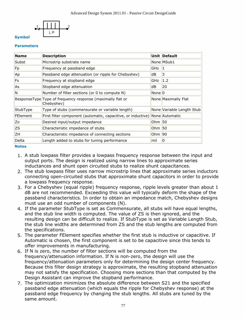
Advanced Design System 2011.01 - Passive Circuit DesignGuide
77
Symbol
Parameters
Name Description Unit Default
Subst Microstrip substrate name None MSub1
Fp Frequency at passband edge GHz 1
Ap Passband edge attenuation (or ripple for Chebyshev) dB 3
Fs Frequency at stopband edge GHz 1.2
As Stopband edge attenuation dB 20
N Number of filter sections (or 0 to compute N) None 0
ResponseType Type of frequency response (maximally flat orChebyshev)
None Maximally Flat
StubType Type of stubs (commensurate or variable length) None Variable Length Stub
FElement First filter component (automatic, capacitive, or inductive) None Automatic
Zo Desired input/output impedance Ohm 50
ZS Characteristic impedance of stubs Ohm 50
ZH Characteristic impedance of connecting sections Ohm 90
Delta Length added to stubs for tuning performance mil 0
Notes
A stub lowpass filter provides a lowpass frequency response between the input and1.output ports. The design is realized using narrow lines to approximate seriesinductances and shunt open circuited stubs to realize shunt capacitances.The stub lowpass filter uses narrow microstrip lines that approximate series inductors2.connecting open-circuited stubs that approximate shunt capacitors in order to providea lowpass frequency response.For a Chebyshev (equal ripple) frequency response, ripple levels greater than about 13.dB are not recommended. Exceeding this value will typically deform the shape of thepassband characteristics. In order to obtain an impedance match, Chebyshev designsmust use an odd number of components (N).If the parameter StubType is set as Commensurate, all stubs will have equal lengths,4.and the stub line width is computed. The value of ZS is then ignored, and theresulting design can be difficult to realize. If StubType is set as Variable Length Stub,the stub line widths are determined from ZS and the stub lengths are computed fromthe specifications.The parameter FElement specifies whether the first stub is inductive or capacitive. If5.Automatic is chosen, the first component is set to be capacitive since this tends tooffer improvements in manufacturing.If N is zero, the number of filter sections will be computed from the6.frequency/attenuation information. If N is non-zero, the design will use thefrequency/attenuation parameters only for determining the design center frequency.Because this filter design strategy is approximate, the resulting stopband attenuationmay not satisfy the specification. Choosing more sections than that computed by theDesign Assistant can improve the stopband performance.The optimization minimizes the absolute difference between S21 and the specified7.passband edge attenuation (which equals the ripple for Chebyshev response) at thepassband edge frequency by changing the stub lengths. All stubs are tuned by thesame amount.
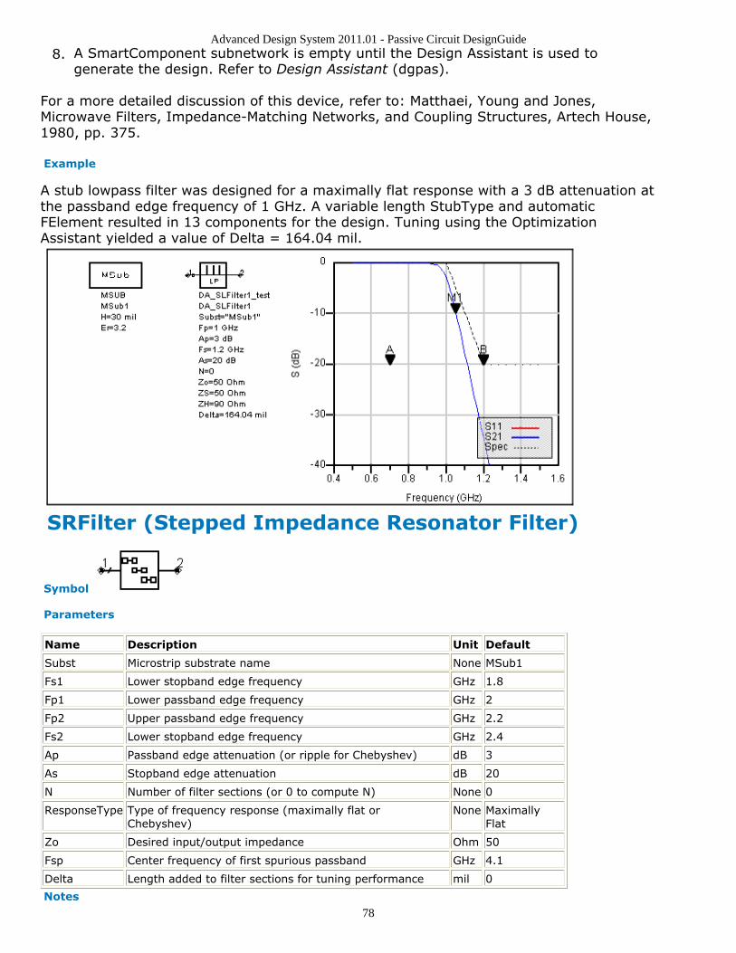
Advanced Design System 2011.01 - Passive Circuit DesignGuide
78
A SmartComponent subnetwork is empty until the Design Assistant is used to8.generate the design. Refer to Design Assistant (dgpas).
For a more detailed discussion of this device, refer to: Matthaei, Young and Jones,Microwave Filters, Impedance-Matching Networks, and Coupling Structures, Artech House,1980, pp. 375.
Example
A stub lowpass filter was designed for a maximally flat response with a 3 dB attenuation atthe passband edge frequency of 1 GHz. A variable length StubType and automaticFElement resulted in 13 components for the design. Tuning using the OptimizationAssistant yielded a value of Delta = 164.04 mil.
SRFilter (Stepped Impedance Resonator Filter)
Symbol
Parameters
Name Description Unit Default
Subst Microstrip substrate name None MSub1
Fs1 Lower stopband edge frequency GHz 1.8
Fp1 Lower passband edge frequency GHz 2
Fp2 Upper passband edge frequency GHz 2.2
Fs2 Lower stopband edge frequency GHz 2.4
Ap Passband edge attenuation (or ripple for Chebyshev) dB 3
As Stopband edge attenuation dB 20
N Number of filter sections (or 0 to compute N) None 0
ResponseType Type of frequency response (maximally flat orChebyshev)
None MaximallyFlat
Zo Desired input/output impedance Ohm 50
Fsp Center frequency of first spurious passband GHz 4.1
Delta Length added to filter sections for tuning performance mil 0
Notes

Advanced Design System 2011.01 - Passive Circuit DesignGuide
79
A stepped impedance resonator filter provides a bandpass frequency response1.between the input and output ports. N coupled-line sections produce an N−1 orderfilter response. Additional numbers of sections can be used to steepen the transitionband roll off or widen the pass bandwidth. The use on non-uniform impedance foreach resonator moves the second pass band center frequency away from the secondharmonic of the fundamental frequency.Because of the heavy computational burden in determining the line parameters, a2.brief delay will occur for the design.For a Chebyshev (equal ripple) frequency response, ripple levels greater than about 13.dB are not recommended. Exceeding this value will typically deform the shape of thepassband characteristics.If N is zero, the number of filter sections will be computed from the4.frequency/attenuation information. If N is non-zero, the design will use thefrequency/attenuation parameters only for determining the design center frequency.The center frequency of the first spurious passband should be on the order of twice5.the fundamental passband center frequency.The optimization minimizes the absolute difference between S21 in dB and the6.specified passband edge attenuation (which equals the ripple for Chebyshevresponse) at the passband edge frequencies. Because only the line lengths arechanged, this tuning will typically center the response within the specified passband.More advanced shaping of the passband response can be accomplished by manuallytuning the widths and spacings of the coupled filter sections.A SmartComponent subnetwork is empty until the Design Assistant is used to7.generate the design. Refer to Design Assistant (dgpas).
For a more detailed discussion of this device, refer to: Makimoto and Yamashita,"Bandpass filters using parallel coupled stripline stepped impedance resonators," IEEETrans. Microwave Theory and Techniques , vol MTT-28, pp. 1413-1417, 1980.
Example
A stepped impedance resonator filter was designed for a maximally flat response with the3 dB passband edge frequencies at 2 GHz and 2.2 GHz respectively. The second passbandwas set to 4.1 GHz. The design required 4 coupled lines. Tuning using the OptimizationAssistant yielded a value of Delta = 0.785 mil.
SSMatch (Single-Stub Match)
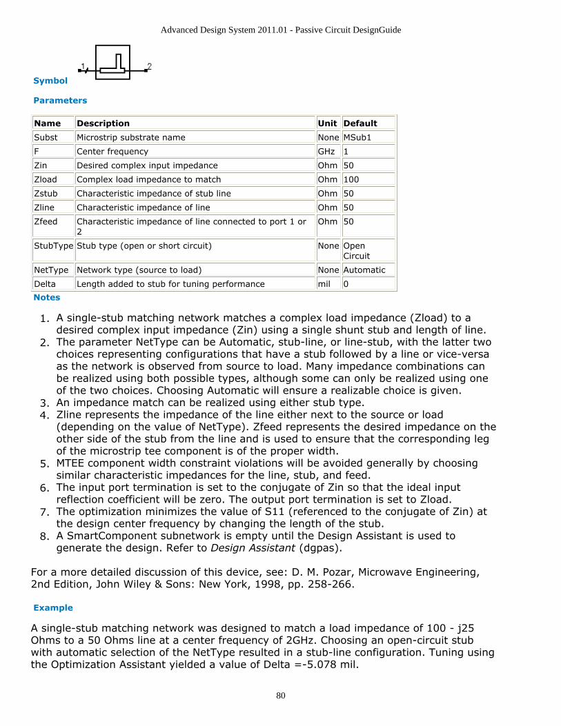
Advanced Design System 2011.01 - Passive Circuit DesignGuide
80
Symbol
Parameters
Name Description Unit Default
Subst Microstrip substrate name None MSub1
F Center frequency GHz 1
Zin Desired complex input impedance Ohm 50
Zload Complex load impedance to match Ohm 100
Zstub Characteristic impedance of stub line Ohm 50
Zline Characteristic impedance of line Ohm 50
Zfeed Characteristic impedance of line connected to port 1 or2
Ohm 50
StubType Stub type (open or short circuit) None OpenCircuit
NetType Network type (source to load) None Automatic
Delta Length added to stub for tuning performance mil 0
Notes
A single-stub matching network matches a complex load impedance (Zload) to a1.desired complex input impedance (Zin) using a single shunt stub and length of line.The parameter NetType can be Automatic, stub-line, or line-stub, with the latter two2.choices representing configurations that have a stub followed by a line or vice-versaas the network is observed from source to load. Many impedance combinations canbe realized using both possible types, although some can only be realized using oneof the two choices. Choosing Automatic will ensure a realizable choice is given.An impedance match can be realized using either stub type.3.Zline represents the impedance of the line either next to the source or load4.(depending on the value of NetType). Zfeed represents the desired impedance on theother side of the stub from the line and is used to ensure that the corresponding legof the microstrip tee component is of the proper width.MTEE component width constraint violations will be avoided generally by choosing5.similar characteristic impedances for the line, stub, and feed.The input port termination is set to the conjugate of Zin so that the ideal input6.reflection coefficient will be zero. The output port termination is set to Zload.The optimization minimizes the value of S11 (referenced to the conjugate of Zin) at7.the design center frequency by changing the length of the stub.A SmartComponent subnetwork is empty until the Design Assistant is used to8.generate the design. Refer to Design Assistant (dgpas).
For a more detailed discussion of this device, see: D. M. Pozar, Microwave Engineering,2nd Edition, John Wiley & Sons: New York, 1998, pp. 258-266.
Example
A single-stub matching network was designed to match a load impedance of 100 - j25Ohms to a 50 Ohms line at a center frequency of 2GHz. Choosing an open-circuit stubwith automatic selection of the NetType resulted in a stub-line configuration. Tuning usingthe Optimization Assistant yielded a value of Delta =-5.078 mil.

Advanced Design System 2011.01 - Passive Circuit DesignGuide
81
TCoupler (Tee Power Divider)
Symbol
Parameters
Name Description Unit Default
Subst Microstrip substrate name None MSub1
F Center frequency GHz 1
Zo1 Characteristic impedance of input port 1 Ohm 50
Zo2 Characteristic impedance of output port 2 Ohm 50
Zo3 Characteristic impedance of output port 3 Ohm 50
K Ratio of power out port 2 to power out port 3 None 1.0
Delta Length added to quarter-wave sections for tuningperformance
mil 0
Notes
A tee power divider splits the power at the input (pin 1) between the two outputs1.(pins 2 and 3). Unequal or equal power splits can be realized. The input port will bematched to its feeding line, although in general the output ports will not be matched.The value of K can be set to realize the desired power split out of ports 2 and 3.2.However, choosing K larger than 3 to 4 (or smaller than 1/3 to 1/4) can cause theratio of the widths of the tee branches to violate the range of the MTEE simulationmodel. While the simulation will still proceed, the results can have some inaccuracies.Quarter-wave matching sections are provided on the output ports to ensure a proper3.power split is achieved.The optimization minimizes the input reflection coefficient (S11) at the design center4.frequency by changing the length of the quarter wave transformers on the outputlegs.A SmartComponent subnetwork is empty until the Design Assistant is used to5.generate the design. Refer to Design Assistant (dgpas).
For a more detailed discussion of this device, see: D. M. Pozar, Microwave Engineering,

Advanced Design System 2011.01 - Passive Circuit DesignGuide
82
2nd Edition, John Wiley & Sons: New York, 1998, pp. 360-361.
Example
A tee power divider was designed for a center frequency of 1 GHz with an unequal powersplit (K=3.5). Tuning using the Optimization Assistant yielded a value of Delta = -34.633mil.
TLMatch (Tapered-Line Match)
Symbol
Parameters
Name Description Unit Default
Subst Microstrip substrate name None MSub1
F Design frequency GHz 1
Zo Desired input impedance Ohm 50
Rload Load impedance to match Ohm 100
ResponseType Type of frequency response (exponential, triangular, Klopfenstein) None Exponential
L Length of tapered line in wavelengths at frequency F (set L=0 to compute L) None 0.0
Rmax Maximum voltage reflection coefficient None 0.1
NSection Number of linear taper sections per wavelength None 20
Notes
A tapered-line matching network matches a real load impedance (Rload) to a desired1.real input impedance (Zo) using a continuously varying line characteristic impedanceto realize a specified frequency response. The reflection coefficient remains below thespecified maximum value for all frequencies above the design frequency.The continuous impedance taper of this circuit is approximated using a sequence of2.linear tapers. Increasing the number of sections per wavelength (NSection) willimprove the approximation to the defined taper.If the length of the line L is set to zero, the Design Assistant chooses L such that the3.reflection coefficient is less than Rmax for all frequencies above the design frequency.

Advanced Design System 2011.01 - Passive Circuit DesignGuide
83
Otherwise, Rmax is ignored.The ResponseType specifies the distribution of the impedance along the length of the4.line and therefore determines the frequency response of the match.No Optimization Assistant is provided since the design process is exact to within the5.approximation of the continuous impedance taper using multiple linear tapersegments. Increasing the value of NSection will improve the computed response.A SmartComponent subnetwork is empty until the Design Assistant is used to6.generate the design. Refer to Design Assistant (dgpas).
For a more detailed discussion of this device, see: D. M. Pozar, Microwave Engineering,2nd Edition, John Wiley & Sons: New York, 1998, pp. 288-295.
Example
A tapered-line matching network was designed to match a load impedance of 100 Ohms toa 50 Ohms line at a center frequency of 4 GHz. Specifying a Klopfenstein frequencyresponse for which the reflection coefficient remains below 0.1 along with 30 sections perwavelength dictates 18 tapered-line sections to realize the match. The plot has beenshown in linear magnitude rather than dB to emphasize the equal-ripple frequencyresponse.
WDCoupler (Wilkinson Divider)
Symbol
Parameters
Advanced Design System 2011.01 - Passive Circuit DesignGuide
84
Name Description Unit Default
Subst Microstrip substrate name None MSub1
F Center frequency GHz 1
DeltaF Frequency bandwidth GHz 0.5
Zo Characteristic impedance Ohm 50
ResponseType Type of frequency response None Uniform
N Number of quarter-wave sections; set N=0 to compute N None 0
Rmax Maximum voltage reflection coefficient on input port None 0.1
K Ratio of power out port 2 to power out port 3 None 1.0
Wgap Width of gap for resistor mil 50
Delta Length added to quarter-wave branches for tuning performance mil 0
Notes
A Wilkinson power divider splits the power at the input (pin 1) between the two1.outputs (pins 2 and 3). Unequal or equal power splits can be realized. The signals atthe outputs are in phase. All three ports will be matched, and ports 2 and 3 will ingeneral be well isolated from each other.For broadband performance, the divider can have multiple quarter-wave sections. If2.the number of sections N is set to zero, the Design Assistant chooses N such thatsuch that the reflection coefficient is less than Rmax over the bandwidth DeltaF(centered at the design center frequency). the resulting bandwidth can be broaderthan that specified. Otherwise, Rmax and DeltaF are ignored.ResponseType specifies the distribution of the partial reflection coefficients seen at3.each section interface - Uniform, Binomial, and Chebyshev distributions are available.These in turn specify the shape of the reflection coefficient versus frequency.For a single section divider (N=1), the value of K can be set to realize the desired4.power split out of ports 2 and 3. Be aware that choosing K larger than 3 to 4 (orsmaller than 1/3 to 1/4) is likely to cause difficulties in the design.Pozar specifies K2= P3/P2, while the DesignGuide uses K2= P2/P3. Therefore, if you5.use the equations in Pozar to verify everything, you must substitute 1/K for K. TheDesignGuide automatically puts quarter-wave matching sections on ports 2 and 3, soall ports are matched to the characteristic impedance. If you remove these matchingsegments, the output impedances are those specified by Pozar.The optimization minimizes the input reflection coefficient (S11) at the design center6.frequency by changing the length of the quarter wave branches forming the divider.A SmartComponent subnetwork is empty until the Design Assistant is used to7.generate the design. Refer to Design Assistant (dgpas).
For a more detailed discussion of this device, see: D. M. Pozar, Microwave Engineering,2nd Edition, John Wiley & Sons: New York, 1998, pp. 363-368.
Example
A single-section Wilkinson power divider (N=1) was designed for a center frequency of 5GHz with an equal power split (K=1) and a gap width for the resistor of 50 mil. Tuningusing the Optimization Assistant yielded a value of Delta = 58.03 mil.

Advanced Design System 2011.01 - Passive Circuit DesignGuide
85
ZZFilter (Zig-Zag Coupled-Line Filter)
Symbol
Parameters
Name Description Unit Default
Subst Microstrip substrate name None MSub1
Fs1 Lower stopband edge frequency GHz 1.8
Fp1 Lower passband edge frequency GHz 2
Fp2 Upper passband edge frequency GHz 2.2
Ap Passband edge attenuation (or ripple for Chebyshev) dB 2.4
As Stopband edge attenuation dB 3
N Number of filter sections (or 0 to compute N) None 20
ResponseType Type of frequency response (maximally flat orChebyshev)
None 0
Zo Desired input/output impedance Ohm MaximallyFlat
Delta Length added to coupled sections for tuning performance mil 0
Notes
A zig-zag coupled-line filter provides a bandpass frequency response between the1.input and output ports. The design uses a coupled-line filter topology but includes 90degree bend between each coupled section so that the layout is more compact.Because of the heavy computational burden in determining the line parameters, a2.brief delay will occur for the design.For a Chebyshev (equal ripple) frequency response, ripple levels greater than about 13.dB are not recommended. Exceeding this value will typically deform the shape of thepassband characteristics.If N is zero, the number of filter sections will be computed from the4.frequency/attenuation information. If N is non-zero, the design will use thefrequency/attenuation parameters only for determining the design center frequency.The optimization minimizes the absolute difference between S21 and the specified5.
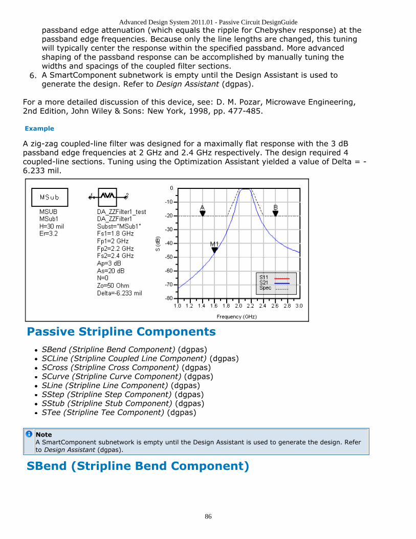
Advanced Design System 2011.01 - Passive Circuit DesignGuide
86
passband edge attenuation (which equals the ripple for Chebyshev response) at thepassband edge frequencies. Because only the line lengths are changed, this tuningwill typically center the response within the specified passband. More advancedshaping of the passband response can be accomplished by manually tuning thewidths and spacings of the coupled filter sections.A SmartComponent subnetwork is empty until the Design Assistant is used to6.generate the design. Refer to Design Assistant (dgpas).
For a more detailed discussion of this device, see: D. M. Pozar, Microwave Engineering,2nd Edition, John Wiley & Sons: New York, 1998, pp. 477-485.
Example
A zig-zag coupled-line filter was designed for a maximally flat response with the 3 dBpassband edge frequencies at 2 GHz and 2.4 GHz respectively. The design required 4coupled-line sections. Tuning using the Optimization Assistant yielded a value of Delta = -6.233 mil.
Passive Stripline ComponentsSBend (Stripline Bend Component) (dgpas)SCLine (Stripline Coupled Line Component) (dgpas)SCross (Stripline Cross Component) (dgpas)SCurve (Stripline Curve Component) (dgpas)SLine (Stripline Line Component) (dgpas)SStep (Stripline Step Component) (dgpas)SStub (Stripline Stub Component) (dgpas)STee (Stripline Tee Component) (dgpas)
NoteA SmartComponent subnetwork is empty until the Design Assistant is used to generate the design. Referto Design Assistant (dgpas).
SBend (Stripline Bend Component)
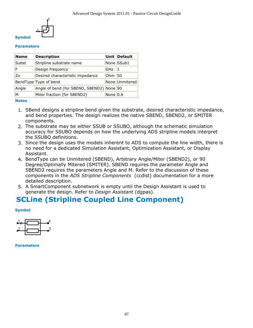
Advanced Design System 2011.01 - Passive Circuit DesignGuide
87
Symbol
Parameters
Name Description Unit Default
Subst Stripline substrate name None SSub1
F Design frequency GHz 1
Zo Desired characteristic impedance Ohm 50
BendType Type of bend None Unmitered
Angle Angle of bend (for SBEND, SBEND2) None 90
M Miter fraction (for SBEND2) None 0.6
Notes
SBend designs a stripline bend given the substrate, desired characteristic impedance,1.and bend properties. The design realizes the native SBEND, SBEND2, or SMITERcomponents.The substrate may be either SSUB or SSUBO, although the schematic simulation2.accuracy for SSUBO depends on how the underlying ADS stripline models interpretthe SSUBO definitions.Since the design uses the models inherent to ADS to compute the line width, there is3.no need for a dedicated Simulation Assistant, Optimization Assistant, or DisplayAssistant.BendType can be Unmitered (SBEND), Arbitrary Angle/Miter (SBEND2), or 904.Degree/Optimally Mitered (SMITER). SBEND requires the parameter Angle andSBEND2 requires the parameters Angle and M. Refer to the discussion of thesecomponents in the ADS Stripline Components (ccdist) documentation for a moredetailed description.A SmartComponent subnetwork is empty until the Design Assistant is used to5.generate the design. Refer to Design Assistant (dgpas).
SCLine (Stripline Coupled Line Component) Symbol
Parameters
Advanced Design System 2011.01 - Passive Circuit DesignGuide
88
Name Description Unit Default
Subst Stripline substrate name None SSub1
F Design frequency GHz 1
Zoe Even-mode characteristic impedance Ohm 55
Zoo Odd-mode characteristic impedance Ohm 45
Zo1 Characteristic impedance of input line at port 1 Ohm 50
Zo2 Characteristic impedance of input line at port 2 Ohm 50
Zo3 Characteristic impedance of input line at port 3 Ohm 50
Zo4 Characteristic impedance of input line at port 4 Ohm 50
Lphys Physical line length; set to zero if Lelec specified mil 0
Lelec Line length in wavelengths; set to zero if Lphysspecified
None 0.25
Notes
SCLine designs a stripline coupled line component given the substrate, desired even-1.and odd-mode characteristic impedances, and physical or electrical length.The substrate may be either SSUB or SSUBO, although the schematic simulation2.accuracy for SSUBO depends on how the underlying ADS stripline models interpretthe SSUBO definitions.Since the design uses the models inherent to ADS to compute the line width, there is3.no need for a dedicated Simulation Assistant, Optimization Assistant, or DisplayAssistant.For proper operation, either Lphys or Lelec must be zero.4.Zo1 through Zo4 specify the impedance of the lines attached to this component and5.are provided to ensure proper pin location in the layout. Refer to the discussion ofthe SCLIN component in the ADS Stripline Components (ccdist) documentation for amore detailed description of the model used for this component.A SmartComponent subnetwork is empty until the Design Assistant is used to6.generate the design. Refer to Design Assistant (dgpas).
SCross (Stripline Cross Component)
Symbol
Parameters
Name Description Unit Default
Subst Stripline substrate name None SSub1
F Design frequency GHz 1
Z1 Characteristic impedance of port1
Ohm 50
Z2 Characteristic impedance of port2
Ohm 50
Z3 Characteristic impedance of port3
Ohm 50
Z4 Characteristic impedance of port4
Ohm 50
Notes
SCross designs a stripline cross given the substrate and desired characteristic1.
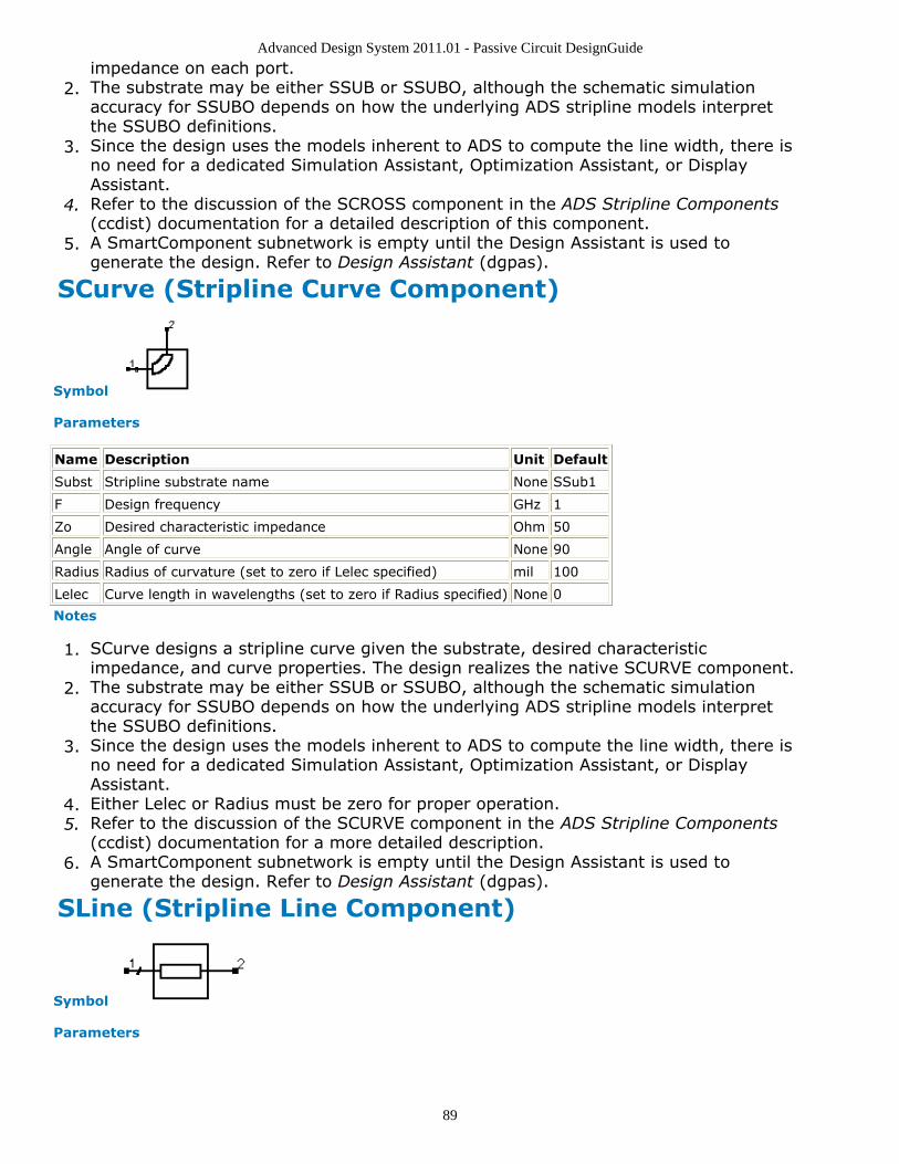
Advanced Design System 2011.01 - Passive Circuit DesignGuide
89
impedance on each port.The substrate may be either SSUB or SSUBO, although the schematic simulation2.accuracy for SSUBO depends on how the underlying ADS stripline models interpretthe SSUBO definitions.Since the design uses the models inherent to ADS to compute the line width, there is3.no need for a dedicated Simulation Assistant, Optimization Assistant, or DisplayAssistant.Refer to the discussion of the SCROSS component in the ADS Stripline Components4.(ccdist) documentation for a detailed description of this component.A SmartComponent subnetwork is empty until the Design Assistant is used to5.generate the design. Refer to Design Assistant (dgpas).
SCurve (Stripline Curve Component)
Symbol
Parameters
Name Description Unit Default
Subst Stripline substrate name None SSub1
F Design frequency GHz 1
Zo Desired characteristic impedance Ohm 50
Angle Angle of curve None 90
Radius Radius of curvature (set to zero if Lelec specified) mil 100
Lelec Curve length in wavelengths (set to zero if Radius specified) None 0
Notes
SCurve designs a stripline curve given the substrate, desired characteristic1.impedance, and curve properties. The design realizes the native SCURVE component.The substrate may be either SSUB or SSUBO, although the schematic simulation2.accuracy for SSUBO depends on how the underlying ADS stripline models interpretthe SSUBO definitions.Since the design uses the models inherent to ADS to compute the line width, there is3.no need for a dedicated Simulation Assistant, Optimization Assistant, or DisplayAssistant.Either Lelec or Radius must be zero for proper operation.4.Refer to the discussion of the SCURVE component in the ADS Stripline Components5.(ccdist) documentation for a more detailed description.A SmartComponent subnetwork is empty until the Design Assistant is used to6.generate the design. Refer to Design Assistant (dgpas).
SLine (Stripline Line Component)
Symbol
Parameters
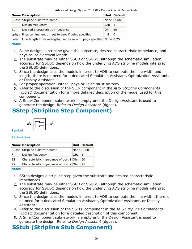
Advanced Design System 2011.01 - Passive Circuit DesignGuide
90
Name Description Unit Default
Subst Stripline substrate name None SSub1
F Design frequency GHz 1
Zo Desired characteristic impedance Ohm 50
Lphys Physical line length; set to zero if Lelec specified mil 0
Lelec Line length in wavelengths; set to zero if Lphys specified None 0.25
Notes
SLine designs a stripline given the substrate, desired characteristic impedance, and1.physical or electrical length.The substrate may be either SSUB or SSUBO, although the schematic simulation2.accuracy for SSUBO depends on how the underlying ADS stripline models interpretthe SSUBO definitions.Since the design uses the models inherent to ADS to compute the line width and3.length, there is no need for a dedicated Simulation Assistant, Optimization Assistant,or Display Assistant.For proper operation, either Lphys or Lelec must be zero.4.Refer to the discussion of the SLIN component in the ADS Stripline Components5.(ccdist) documentation for a more detailed description of the model used for thiscomponent.A SmartComponent subnetwork is empty until the Design Assistant is used to6.generate the design. Refer to Design Assistant (dgpas).
SStep (Stripline Step Component)
Symbol
Parameters
Name Description Unit Default
Subst Stripline substrate name None SSub1
F Design frequency GHz 1
Z1 Characteristic impedance of port 1 Ohm 50
Z2 Characteristic impedance of port 2 Ohm 25
Notes
SStep designs a stripline step given the substrate and desired characteristic1.impedances.The substrate may be either SSUB or SSUBO, although the schematic simulation2.accuracy for SSUBO depends on how the underlying ADS stripline models interpretthe SSUBO definitions.Since the design uses the models inherent to ADS to compute the line width, there is3.no need for a dedicated Simulation Assistant, Optimization Assistant, or DisplayAssistant.Refer to the discussion of the SSTEP component in the ADS Stripline Components4.(ccdist) documentation for a detailed description of this component.A SmartComponent subnetwork is empty until the Design Assistant is used to5.generate the design. Refer to Design Assistant (dgpas).
SStub (Stripline Stub Component)

Advanced Design System 2011.01 - Passive Circuit DesignGuide
91
Symbol
Parameters
Name Description Unit Default
Subst Stripline substrate name None SSub1
F Design frequency GHz 1
Zo Desired characteristic impedance Ohm 50
Lphys Physical line length mil 0
Lelec Line length in wavelengths None 0
Xin Desired input reactance Ohm 0
Cin Desired input capacitance pF 0
Lin Desired input inductance nH 0
StubType Type of stub None OpenCircuit
Notes
SStub designs a stripline open or short circuited stub given the substrate, desired1.characteristic impedance, and physical or electrical length. The design realizes thenative SLOC, SLSC, and SLEF components.The substrate may be either SSUB or SSUBO, although the schematic simulation2.accuracy for SSUBO depends on how the underlying ADS stripline models interpretthe SSUBO definitions.Only one of Lphys, Lelec, Xin, Cin, and Lin can be non-zero.3.Since the design uses the models inherent to ADS to compute the line width and4.length, there is no need for a dedicated Simulation Assistant, Optimization Assistant,or Display Assistant.For proper operation, only one of Lphys, Lelec, Xin, Cin, and Lin can be non-zero.5.StubType can be either Open Circuit (SLOC), End Effect (SLEF), or Short Circuit6.(SLSC). Refer to the discussion of these components in the ADS StriplineComponents (ccdist) documentation for a more detailed description of these differentoptions.A SmartComponent subnetwork is empty until the Design Assistant is used to7.generate the design. Refer to Design Assistant (dgpas).
STee (Stripline Tee Component)
Symbol
Parameters
Advanced Design System 2011.01 - Passive Circuit DesignGuide
92
Name Description Unit Default
Subst Stripline substrate name None SSub1
F Design frequency GHz 1
Z1 Characteristic impedance of port1
Ohm 50
Z2 Characteristic impedance of port2
Ohm 50
Z3 Characteristic impedance of port3
Ohm 50
Notes
STee designs a stripline tee given the substrate and desired characteristic impedance1.at each port.The substrate may be either SSUB or SSUBO, although the schematic simulation2.accuracy for SSUBO depends on how the underlying ADS stripline models interpretthe SSUBO definitions.Since the design uses the models inherent to ADS to compute the line width and3.length, there is no need for a dedicated Simulation Assistant, Optimization Assistant,or Display Assistant.Z1, Z2, and Z3 are used to determine the widths of each port. Refer to the discussion4.of the STEE component in the ADS Stripline Components (ccdist) documentation for amore detailed description of this component.A SmartComponent subnetwork is empty until the Design Assistant is used to5.generate the design. Refer to Design Assistant (dgpas).
Passive Stripline Circuits
SBLCoupler (Stripline Branch-Line Coupler) (dgpas)SCLCoupler (Stripline Coupled-Line Coupler) (dgpas)SCLFilter (Stripline Coupled-Line Filter) (dgpas)SCMFilter (Stripline Comb-Line Filter) (dgpas)SDSMatch (Stripline Double-Stub Match) (dgpas)SHPFilter (Stripline Hairpin Filter) (dgpas)SIDFilter (Stripline Interdigital Filter) (dgpas)SQWMatch (Stripline Quarter-Wave Match) (dgpas)SRRCoupler (Stripline Rat-Race Coupler) (dgpas)SSBFilter (Stripline Stub Bandpass Filter) (dgpas)SSIFilter (Stripline Stepped Impedance Lowpass Filter) (dgpas)SSLFilter (Stripline Stub Lowpass Filter) (dgpas)SSRFilter (Stripline Stepped Impedance Resonator Filter) (dgpas)SSSMatch (Stripline Single-Stub Match) (dgpas)STCoupler (Stripline Tee Power Divider) (dgpas)SWDCoupler (Stripline Wilkinson Divider) (dgpas)
SBLCoupler (Stripline Branch-Line Coupler)
Symbol
Parameters

Advanced Design System 2011.01 - Passive Circuit DesignGuide
93
Name Description Unit Default
Subst Stripline substrate name None SSub1
F Center frequency GHz 1
DeltaF Total frequency bandwidth GHz 0.5
Zo Characteristic impedance Ohm 50
ResponseType Type of frequency response None Chebyshev
N Number of coupler sections; set N=0 to computeN
None 0
Rmax Maximum voltage reflection coefficient at the input None 0.5
C Coupling coefficient dB 3
Delta Length added to branches for tuning performance mil 0
Notes
A branch-line coupler outputs from the coupled port (pin 3) a fraction of the power1.presented at the input (pin 1). The remainder of the power is passed through to theoutput port (pin 2). At the center frequency the phase difference between theoutputs is 90 degrees, with the coupled port representing the quadrature (Q) outputand the output port representing the in-phase (I) output. The coupling coefficientspecifies the ratio of the input power to the coupled power (P1/P3). Pin 4 represents
the isolated port, and it is typically well isolated from the input port near the centerfrequency.The substrate may be either SSUB or SSUBO, although the schematic simulation2.accuracy for SSUBO depends on how the underlying ADS stripline models interpretthe SSUBO definitions.The coupling coefficient must be positive and greater than 3 dB. Best results are3.obtained for tight couplings of 6 dB or better (C < 6 dB). Choosing the couplingparameter larger than 6 dB often causes width constraint violations to occur on theSTEE components, resulting in warning messages during design and simulation. Acoupling coefficient of 3 dB provides an equal power split between the two outputs.For broadband performance, the coupler can have multiple sections. If the number of4.sections N is set to zero, the Design Assistant chooses N such that the reflectioncoefficient is less than Rmax over the bandwidth DeltaF (centered at the designcenter frequency). The resulting bandwidth can be broader than that specified.Otherwise, rmax and DeltaF are ignored.The ResponseType specifies the distribution of the partial reflection coefficients seen5.at each section interface - Uniform, Binomial, and Chebyshev distributions areavailable.The optimization minimizes the input reflection coefficient (S11) at the design center6.frequency by changing the length of the lines forming the four branches. All branchesare changed by the same physical length during the optimization.This optimizationgenerally provides very good results but can not guarantee that the specifiedcoupling is attained at the design frequency. More advanced tuning can be performedby changing line width of the branch lines.A SmartComponent subnetwork is empty until the Design Assistant is used to7.generate the design. Refer to Design Assistant (dgpas).
For a more detailed discussion of this device, see: D. M. Pozar, Microwave Engineering,2nd Edition, John Wiley & Sons: New York, 1998, pp. 379-383.
Example

Advanced Design System 2011.01 - Passive Circuit DesignGuide
94
A single-section branch-line coupler was designed for a center frequency of 5 GHz with anequal power split between the I and Q ports. Tuning using the Optimization Assistantyielded a value of Delta = 36.093 mil.
SCLCoupler (Stripline Coupled-Line Coupler)
Symbol
Parameters
Name Description Unit Default
Subst Stripline substrate name None SSub1
F Center frequency GHz 1
C Coupling coefficient dB 20
Zo Characteristic impedance Ohm 50
Delta Length added to branches for tuningperformance
mil 0
Notes
A coupled-line coupler outputs from the coupled port (pin 4) a fraction of the power1.presented at the input (pin 1). The remainder of the power is passed through to theoutput port (pin 2). The coupling coefficient specifies the ratio of the input power tothe coupled power (P1/P4). The remaining port is isolated, although the isolation is
often similar in value to the coupling coefficient for microstrip realizations.The substrate may be either SSUB or SSUBO, although the schematic simulation2.accuracy for SSUBO depends on how the underlying ADS stripline models interpretthe SSUBO definitions.The optimization minimizes the absolute difference between S41 in dB and the3.specified coupling coefficient at the design center frequency by changing the lengthof the coupled-line section.The coupling coefficient must be positive and greater than 3 dB. Best results are4.obtained for weak couplings of roughly 10 dB or more (C > 10dB). Choosing thecoupling coefficient too small can require a spacing between the coupled lines toosmall to realize.A SmartComponent subnetwork is empty until the Design Assistant is used to5.generate the design. Refer to Design Assistant (dgpas).
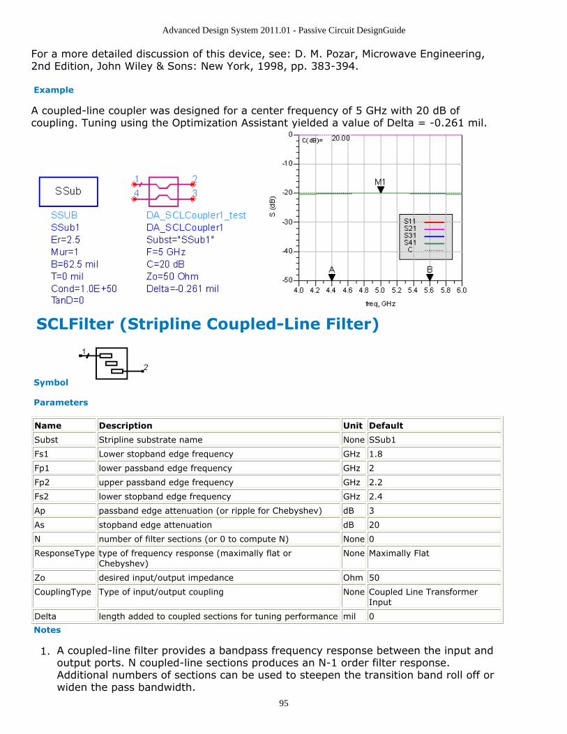
Advanced Design System 2011.01 - Passive Circuit DesignGuide
95
For a more detailed discussion of this device, see: D. M. Pozar, Microwave Engineering,2nd Edition, John Wiley & Sons: New York, 1998, pp. 383-394.
Example
A coupled-line coupler was designed for a center frequency of 5 GHz with 20 dB ofcoupling. Tuning using the Optimization Assistant yielded a value of Delta = -0.261 mil.
SCLFilter (Stripline Coupled-Line Filter)
Symbol
Parameters
Name Description Unit Default
Subst Stripline substrate name None SSub1
Fs1 Lower stopband edge frequency GHz 1.8
Fp1 lower passband edge frequency GHz 2
Fp2 upper passband edge frequency GHz 2.2
Fs2 lower stopband edge frequency GHz 2.4
Ap passband edge attenuation (or ripple for Chebyshev) dB 3
As stopband edge attenuation dB 20
N number of filter sections (or 0 to compute N) None 0
ResponseType type of frequency response (maximally flat orChebyshev)
None Maximally Flat
Zo desired input/output impedance Ohm 50
CouplingType Type of input/output coupling None Coupled Line TransformerInput
Delta length added to coupled sections for tuning performance mil 0
Notes
A coupled-line filter provides a bandpass frequency response between the input and1.output ports. N coupled-line sections produces an N-1 order filter response.Additional numbers of sections can be used to steepen the transition band roll off orwiden the pass bandwidth.
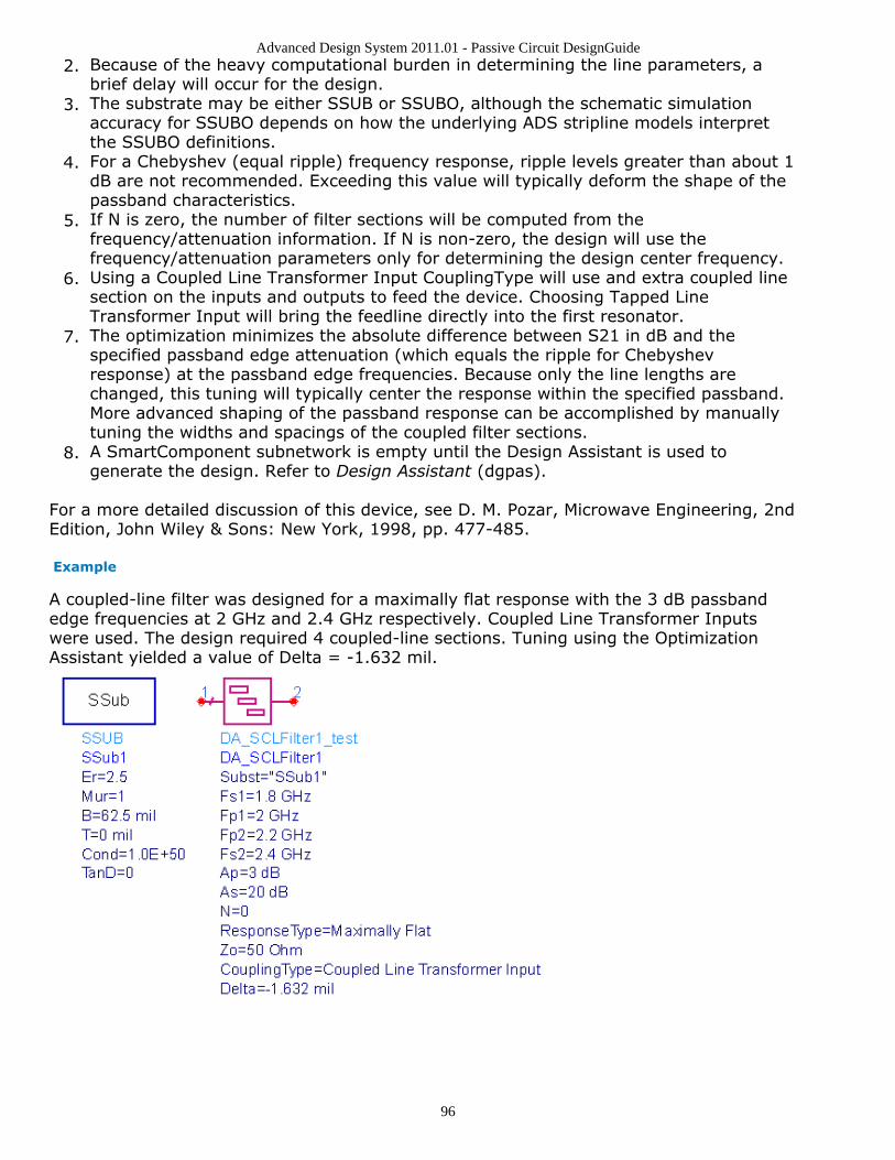
Advanced Design System 2011.01 - Passive Circuit DesignGuide
96
Because of the heavy computational burden in determining the line parameters, a2.brief delay will occur for the design.The substrate may be either SSUB or SSUBO, although the schematic simulation3.accuracy for SSUBO depends on how the underlying ADS stripline models interpretthe SSUBO definitions.For a Chebyshev (equal ripple) frequency response, ripple levels greater than about 14.dB are not recommended. Exceeding this value will typically deform the shape of thepassband characteristics.If N is zero, the number of filter sections will be computed from the5.frequency/attenuation information. If N is non-zero, the design will use thefrequency/attenuation parameters only for determining the design center frequency.Using a Coupled Line Transformer Input CouplingType will use and extra coupled line6.section on the inputs and outputs to feed the device. Choosing Tapped LineTransformer Input will bring the feedline directly into the first resonator.The optimization minimizes the absolute difference between S21 in dB and the7.specified passband edge attenuation (which equals the ripple for Chebyshevresponse) at the passband edge frequencies. Because only the line lengths arechanged, this tuning will typically center the response within the specified passband.More advanced shaping of the passband response can be accomplished by manuallytuning the widths and spacings of the coupled filter sections.A SmartComponent subnetwork is empty until the Design Assistant is used to8.generate the design. Refer to Design Assistant (dgpas).
For a more detailed discussion of this device, see D. M. Pozar, Microwave Engineering, 2ndEdition, John Wiley & Sons: New York, 1998, pp. 477-485.
Example
A coupled-line filter was designed for a maximally flat response with the 3 dB passbandedge frequencies at 2 GHz and 2.4 GHz respectively. Coupled Line Transformer Inputswere used. The design required 4 coupled-line sections. Tuning using the OptimizationAssistant yielded a value of Delta = -1.632 mil.

Advanced Design System 2011.01 - Passive Circuit DesignGuide
97
SCMFilter (Stripline Comb-Line Filter)
Symbol
Parameters
Name Description Unit Default
Subst Stripline substrate name None Subst1
Fs1 Lower stopband edge frequency GHz 1.8
Fp1 Lower passband edge frequency GHz 2
Fp2 Upper passband edge frequency GHz 2.2
Fs2 Lower stopband edge frequency GHz 2.4
Ap Passband edge attenuation (or ripple for Chebyshev) dB 3
As Stopband edge attenuation dB 20
N Number of filter sections (or 0 to compute N) None 0
ResponseType Type of frequency response (maximally flat or Chebyshev) None Maximally Flat
Zo Desired input/output impedance Ohm 50
Lelec Electrical length of filter resonators (the units of Leclec are infractions of a wavelength i.e., 0.25=1/4 wavelength)
None 0.05
ya Normalized interior resonator admittance (0 < ya < 1) None 0.7
CouplingType Type of input/output coupling (coupled line or tapped linetransformer)
None Tapped LineTransformer Input
Delta Length added to coupled sections for tuning performance mil 0
Notes
A comb-line filter provides a bandpass frequency response between the input and1.output ports. N coupled-line sections produce an N-1 order filter response. Additionalnumbers of sections can be used to steepen the transition band roll off or widen thepass bandwidth.Because of the heavy computational burden in determining the line parameters, a2.brief delay will occur for the design.A three-layer substrate must be used for this topology.3.For a Chebyshev (equal ripple) frequency response, ripple levels greater than about 14.dB are not recommended. Exceeding this value will typically deform the shape of thepassband characteristics.

Advanced Design System 2011.01 - Passive Circuit DesignGuide
98
If N is zero, the number of filter sections will be computed from the5.frequency/attenuation information. If N is non-zero, the design will use thefrequency/attenuation parameters only for determining the design center frequency.Using a CouplingType of "Coupled Line Transformer Input" will use an extra coupled6.line section on the inputs and outputs to feed the device. Choosing "Tapped LineTransformer Input" will bring the feedline directly into the first resonator.The optimization minimizes the absolute difference between S21 in dB and the7.specified passband edge attenuation (which equals the ripple for Chebyshevresponse) at the passband edge frequencies. Because only the line lengths arechanged, this tuning will typically center the response within the specified passband.More advanced shaping of the passband response can be accomplished by manuallytuning the widths and spacings of the coupled filter sections.A SmartComponent subnetwork is empty until the Design Assistant is used to8.generate the design. Refer to Design Assistant (dgpas).
For a more detailed discussion of this device, refer to: Matthaei, Young and Jones,Microwave Filters, Impedance-Matching Networks, and Coupling Structures, Artech House,1980, pp. 497.
Example
A comb-line filter was designed for a maximally flat response with the 3 dB passband edgefrequencies at 2 GHz and 2.2 GHz respectively. The design required 3 coupled lines.Tuning using the Optimization Assistant yielded a value of Delta = -11.078 mil.

Advanced Design System 2011.01 - Passive Circuit DesignGuide
99
SDSMatch (Stripline Double-Stub Match)
Symbol
Parameters
Name Description Unit Default
Subst Stripline substrate name None SSub1
F Center frequency GHz 1
Zin Desired complex input impedance Ohm 50
Zload Complex load impedance to match Ohm 100
Zstub1 Characteristic impedance of stub line 1 (nearest input) Ohm 50
Zstub2 Characteristic impedance of stub line 2 (nearest output) Ohm 50
Zline Characteristic impedance of line between stubs Ohm 50
Zfeed1 Characteristic impedance of line connected to port 1 Ohm 50
Zfeed2 Characteristic impedance of line connected to port 2 Ohm 50
Stub1Type Stub 1 type (open or short circuit) None OpenCircuit
Stub2Type Stub 2 type (open or short circuit) None OpenCircuit
Delta Length added to stubs for tuning performance mil 0
Notes
A double-stub matching network matches a complex load impedance (Zload) to a1.desired complex input impedance (Zin) using two shunt stubs and a connecting line.The substrate may be either SSUB or SSUBO, although the schematic simulation2.accuracy for SSUBO depends on how the underlying ADS stripline models interpretthe SSUBO definitions.An impedance match can be realized using any combination of stub types, although3.some combinations can be more realizable.Zfeed1 and Zfeed2 are used simply to ensure that the input and output legs of the4.microstrip tee components are of the proper width.The length of the line between the stubs is nominally chosen to be an eighth of a line5.wavelength. However, if this will not realize the match, the length of line is computed

Advanced Design System 2011.01 - Passive Circuit DesignGuide
100
such that the rotated circle on the Smith chart encloses the load admittance.STEE component width constraint violations will be avoided generally by choosing6.similar characteristic impedances for the line, stub, and feed.Since two solutions are possible, the solution that results in the smallest length of7.stub 1 is chosen. For example, if stub 1 is open circuited, the solution for which stub1 must realize a capacitive reactance is chosen.The input port termination is set to the conjugate of Zin so that the ideal input8.reflection coefficient will be zero. The output port termination is set to Zload.The optimization minimizes the value of S11 (referenced to the conjugate of Zin) at9.the design center frequency by changing the length of the stubs. Both stubs aretuned by the same length.A SmartComponent subnetwork is empty until the Design Assistant is used to10.generate the design. Refer to Design Assistant (dgpas).
For a more detailed discussion of this device, see: D. M. Pozar, Microwave Engineering,2nd Edition, John Wiley & Sons: New York, 1998, pp. 266-271.
Example
A double-stub matching network was designed to match a load impedance of 100 - j30Ohms to a 50 Ohm line at a center frequency of 5 GHz with open circuited stubs. Tuningusing the Optimization Assistant yielded a value of Delta =-20.968 mil.
SHPFilter (Stripline Hairpin Filter)
Symbol
Parameters

Advanced Design System 2011.01 - Passive Circuit DesignGuide
101
Name Description Unit Default
Subst Stripline substrate name None SSub1
Fs1 Lower stopband edge frequency GHz 1.8
Fp1 Lower passband edge frequency GHz 2
Fp2 Upper passband edge frequency GHz 2.2
Fs2 Lower stopband edge frequency GHz 2.4
Ap Passband edge attenuation (or ripple for Chebyshev) dB 3
As Stopband edge attenuation dB 20
N Number of filter sections (or 0 to compute N) None 0
ResponseType Type of frequency response (maximally flat or Chebyshev) None Maximally Flat
Zo Desired input/output impedance Ohm 50
Sphys Physical spacing between legs within hairpin resonator; set tozero if Selec specified
mil 0
Selec Spacing between legs within hairpin resonator in wavelengths;set to zero if Sphys specified
None 0.25
CouplingType Type of input/output coupling (coupled line or tapped linetransformer)
None Coupled LineTransmission Input
Delta Length added to coupled sections for tuning performance mil 0
Notes
A hairpin filter provides a bandpass frequency response between the input and output1.ports. N coupled-line sections produce an N-1 order filter response. Additionalnumbers of sections can be used to steepen the transition band roll off or widen thepass bandwidth.The substrate may be either SSUB or SSUBO, although the schematic simulation2.accuracy for SSUBO depends on how the underlying ADS stripline models interpretthe SSUBO definitions.Because of the heavy computational burden in determining the line parameters, a3.brief delay will occur for the design.For a Chebyshev (equal ripple) frequency response, ripple levels greater than about 14.dB are not recommended. Exceeding this value will typically deform the shape of thepassband characteristics.If N is zero, the number of filter sections will be computed from the5.frequency/attenuation information. If N is non-zero, the design will use thefrequency/attenuation parameters only for determining the design center frequency.Using a Coupled Line Transformer Input CouplingType will use and extra coupled line6.section on the inputs and outputs to feed the device. Choosing Tapped LineTransformer Input will bring the feedline directly into the first resonator.The optimization minimizes the absolute difference between S21 in dB and the7.specified passband edge attenuation (which equals the ripple for Chebyshevresponse) at the passband edge frequencies. Because only the line lengths arechanged, this tuning will typically center the response within the specified passband.More advanced shaping of the passband response can be accomplished by manuallytuning the widths and spacings of the coupled filter sections.A SmartComponent subnetwork is empty until the Design Assistant is used to8.generate the design. Refer to Design Assistant (dgpas).
For a more detailed discussion of this device, refer to: Cristal and Frankel, "Hairpin-lineand hybrid hairpin-line/half-wave parallel-coupled-line filters," IEEE Trans. MicrowaveTheory and Techniques, vol MTT-20, pp. 719-728, 1972.
Example
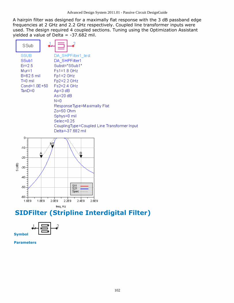
Advanced Design System 2011.01 - Passive Circuit DesignGuide
102
A hairpin filter was designed for a maximally flat response with the 3 dB passband edgefrequencies at 2 GHz and 2.2 GHz respectively. Coupled line transformer inputs wereused. The design required 4 coupled sections. Tuning using the Optimization Assistantyielded a value of Delta = -37.682 mil.
SIDFilter (Stripline Interdigital Filter)
Symbol
Parameters

Advanced Design System 2011.01 - Passive Circuit DesignGuide
103
Name Description Unit Default
Subst Stripline substrate name None Subst1
Fs1 Lower stopband edge frequency GHz 1.8
Fp1 Lower passband edge frequency GHz 2
Fp2 Upper passband edge frequency GHz 2.2
Fs2 Lower stopband edge frequency GHz 2.4
Ap Passband edge attenuation (or ripple for Chebyshev) dB 3
As Stopband edge attenuation dB 20
N Number of filter sections (or 0 to compute N) None 0
ResponseType Type of frequency response (Maximally Flat or Chebyshev) None Maximally Flat
Zo Desired input/output impedance Ohm 50
ya Normalized interior resonator admittance (0 < ya < 1) None 1
CouplingType Type of input/output coupling (coupled line or tapped linetransformer)
None Coupled Line TransformerInput
Delta Length added to coupled sections for tuning performance mil 0
Notes
An interdigital filter provides a bandpass frequency response between the input and1.output ports. N coupled-line sections produce an N-1 order filter response. Additionalnumbers of sections can be used to steepen the transition band roll off or widen thepass bandwidth.Because of the heavy computational burden in determining the line parameters, a2.brief delay will occur for the design.A three-layer substrate must be used for this topology.3.For a Chebyshev (equal ripple) frequency response, ripple levels greater than about 14.dB are not recommended. Exceeding this value will typically deform the shape of thepassband characteristics.If N is zero, the number of filter sections will be computed from the5.frequency/attenuation information. If N is non-zero, the design will use thefrequency/attenuation parameters only for determining the design center frequency.Using a CouplingType of "Coupled Line Transformer Input" will use an extra coupled6.line section on the inputs and outputs to feed the device. Choosing "Tapped LineTransformer Input" will bring the feedline directly into the first resonator.The optimization minimizes the absolute difference between S21 in dB and the7.specified passband edge attenuation (which equals the ripple for Chebyshevresponse) at the passband edge frequencies. Because only the line lengths arechanged, this tuning will typically center the response within the specified passband.More advanced shaping of the passband response can be accomplished by manuallytuning the widths and spacings of the coupled filter sections.A SmartComponent subnetwork is empty until the Design Assistant is used to8.generate the design. Refer to Design Assistant (dgpas).
For a more detailed discussion of this device, refer to: Matthaei, Young and Jones,Microwave Filters, Impedance-Matching Networks, and Coupling Structures, Artech House,1980, pp. 614.
Example
An interdigital filter was designed for a maximally flat response with the 3 dB passbandedge frequencies at 2 GHz and 2.2 GHz respectively. The design required 5 coupled lines.Tuning using the Optimization Assistant yielded a value of Delta = -0.438 mil.
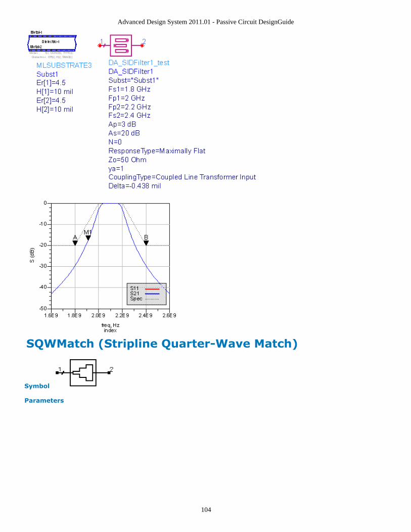
Advanced Design System 2011.01 - Passive Circuit DesignGuide
104
SQWMatch (Stripline Quarter-Wave Match)
Symbol
Parameters

Advanced Design System 2011.01 - Passive Circuit DesignGuide
105
Name Description Unit Default
Subst Stripline substrate name None SSub1
F Center frequency GHz 1
DeltaF Total frequency bandwidth GHz 0.5
Zo Desired input impedance Ohm 50
Rload Load impedance to match Ohm 100
ResponseType Type of frequency response None Uniform
N Number of quarter-wave sections; set N=0 to compute N None 0
Rmax Maximum voltage reflection coefficient None 0.1
Delta Length added to transformer sections for tuning performance mil 0
Notes
A quarter-wave matching network matches a real load impedance (Rload) to a1.desired real input impedance (Zo) using multiple quarter wavelength sections. Aspecified frequency response can be realized by proper design of the individualsections.The substrate may be either SSUB or SSUBO, although the schematic simulation2.accuracy for SSUBO depends on how the underlying ADS stripline models interpretthe SSUBO definitions.DeltaF is defined as the total bandwidth centered at the design center frequency.3.If the number of sections N is set to zero, the Design Assistant chooses N such that4.the reflection coefficient is less that Rmax over the bandwidth DeltaF. The resultingbandwidth may be broader than that specified. Otherwise, Rmax and DeltaF areignored.The ResponseType specifies the distribution of the partial reflection coefficients seen5.at each section interface - Uniform, Binomial, and Chebyshev distributions areavailable. These in turn specify the shape of the reflection coefficient versusfrequency.A single-section quarter-wave matching transformer can be designed by setting N =6.1.Since the reflection coefficient may not be at its minimum value at the design center7.frequency, the optimization centers the variation of S11 (referenced to the value ofZo) versus frequency at the center frequency by changing the length of each quarter-wave section. All sections are tuned by the same length during the optimization.A SmartComponent subnetwork is empty until the Design Assistant is used to8.generate the design. Refer to Design Assistant (dgpas).
For a more detailed discussion of this device, see: D. M. Pozar, Microwave Engineering,2nd Edition, John Wiley & Sons: New York, 1998, pp. 275-288; R. S. Elliott, AnIntroduction to Guided Waves and Microwave Circuits, Prentice Hall, John Wiley, NewJersey, 1993, pp. 218-224.
Example
A quarter-wave matching network was designed to match a load impedance of 100 Ohmsto a 50 Ohm line at a center frequency of 4 GHz. Specifying a Chebyshev frequencyresponse for which the reflection coefficient remains below 0.1 over a 3 GHz bandwidthdictates 3 quarter-wave sections. Tuning using the Optimization Assistant yielded a valueof Delta =-1.544 mil.

Advanced Design System 2011.01 - Passive Circuit DesignGuide
106
SRRCoupler (Stripline Rat-Race Coupler)
Symbol
Parameters
Name Description Unit Default
Subst Stripline substrate name None SSub1
F Center frequency GHz 1
Zo Characteristic impedance Ohm 50
Delta Length added to ring branches fortuning
mil 0
Notes
A rat-race coupler equally divides the power input at port 1 between ports 2 and 3.1.The signal at the output ports 2 and 3 are in-phase. Port 4 is isolated from port 1. Ifthe signal is driven from port 2, then the power is divided between ports 1 and 4 withport 3 isolated. The signal at ports 1 and 4 are 180 degrees out of phase, andtherefore this device is sometimes referred to as a 180-degree hybrid.The substrate may be either SSUB or SSUBO, although the schematic simulation2.accuracy for SSUBO depends on how the underlying ADS stripline models interpretthe SSUBO definitions.The design specifies the width and length of the microstrip lines to ensure that the3.ports are matched to Zo and equal power split is achieved at the design centerfrequency.The optimization minimizes the value of S11 (referenced to the value of Zo) at the4.design center frequency by changing the length of the ring.A SmartComponent subnetwork is empty until the Design Assistant is used to5.generate the design. Refer to Design Assistant (dgpas).
For a more detailed discussion of this device, see: D. M. Pozar, Microwave Engineering,2nd Edition, John Wiley & Sons: New York, 1998, pp. 401-407.
Example
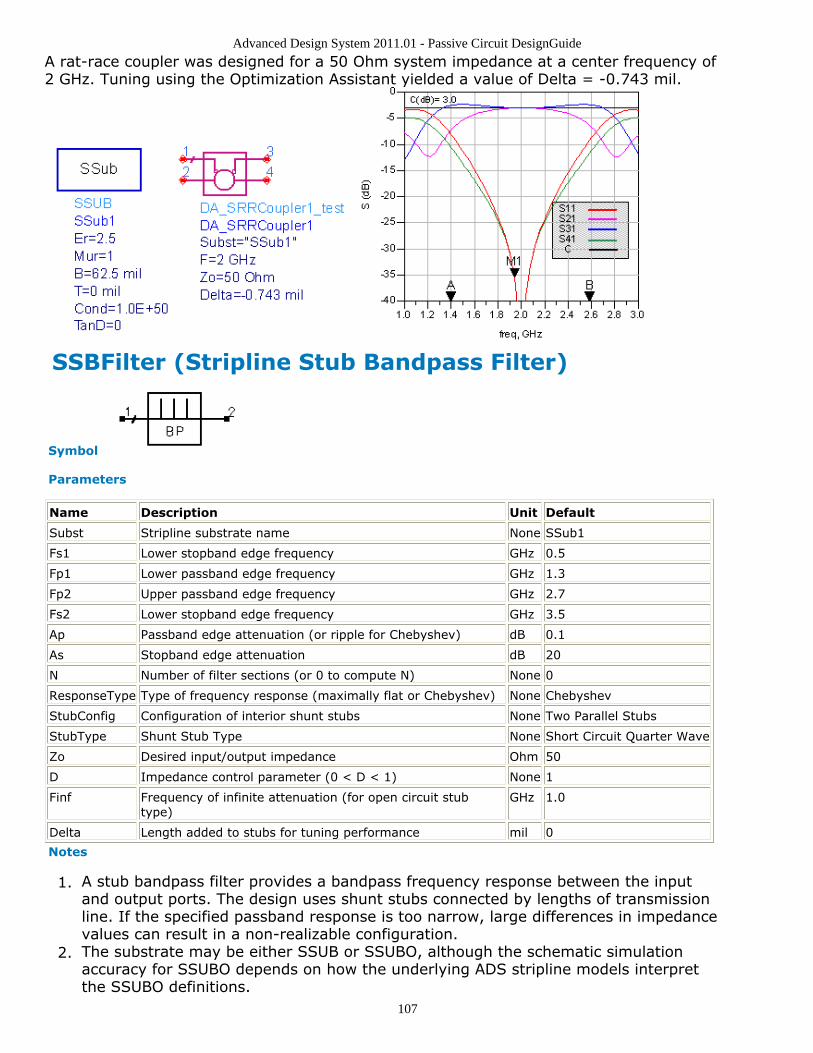
Advanced Design System 2011.01 - Passive Circuit DesignGuide
107
A rat-race coupler was designed for a 50 Ohm system impedance at a center frequency of2 GHz. Tuning using the Optimization Assistant yielded a value of Delta = -0.743 mil.
SSBFilter (Stripline Stub Bandpass Filter)
Symbol
Parameters
Name Description Unit Default
Subst Stripline substrate name None SSub1
Fs1 Lower stopband edge frequency GHz 0.5
Fp1 Lower passband edge frequency GHz 1.3
Fp2 Upper passband edge frequency GHz 2.7
Fs2 Lower stopband edge frequency GHz 3.5
Ap Passband edge attenuation (or ripple for Chebyshev) dB 0.1
As Stopband edge attenuation dB 20
N Number of filter sections (or 0 to compute N) None 0
ResponseType Type of frequency response (maximally flat or Chebyshev) None Chebyshev
StubConfig Configuration of interior shunt stubs None Two Parallel Stubs
StubType Shunt Stub Type None Short Circuit Quarter Wave
Zo Desired input/output impedance Ohm 50
D Impedance control parameter (0 < D < 1) None 1
Finf Frequency of infinite attenuation (for open circuit stubtype)
GHz 1.0
Delta Length added to stubs for tuning performance mil 0
Notes
A stub bandpass filter provides a bandpass frequency response between the input1.and output ports. The design uses shunt stubs connected by lengths of transmissionline. If the specified passband response is too narrow, large differences in impedancevalues can result in a non-realizable configuration.The substrate may be either SSUB or SSUBO, although the schematic simulation2.accuracy for SSUBO depends on how the underlying ADS stripline models interpretthe SSUBO definitions.
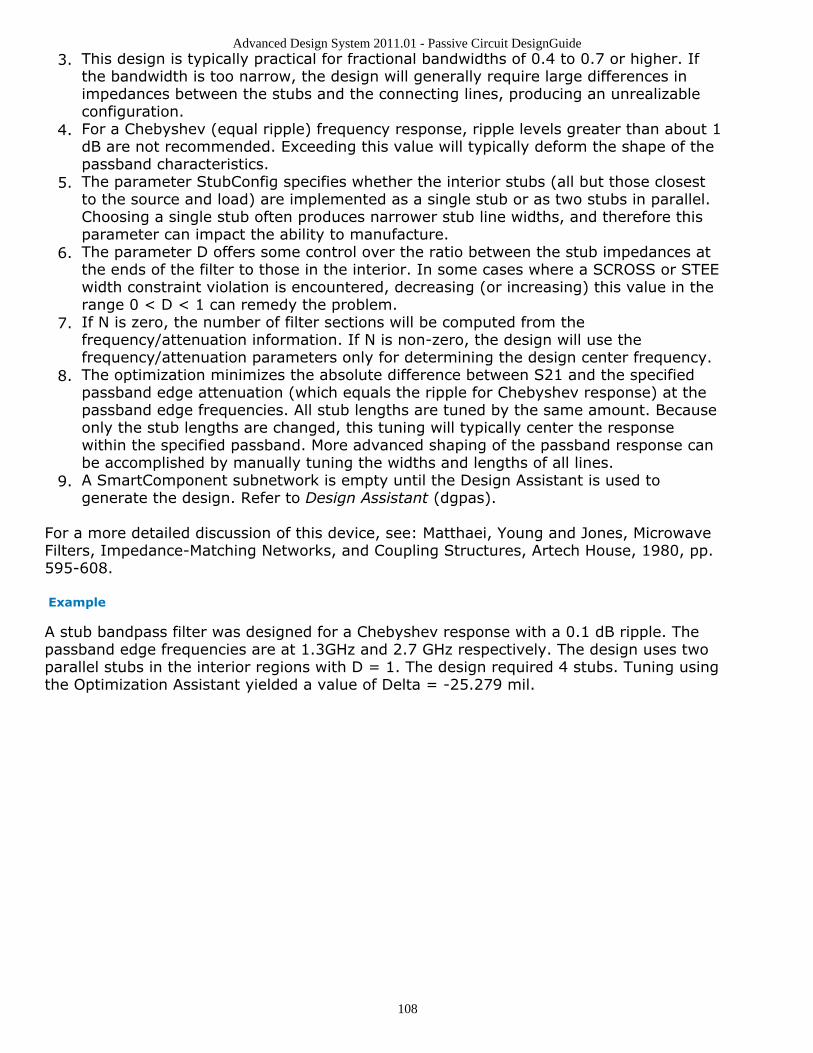
Advanced Design System 2011.01 - Passive Circuit DesignGuide
108
This design is typically practical for fractional bandwidths of 0.4 to 0.7 or higher. If3.the bandwidth is too narrow, the design will generally require large differences inimpedances between the stubs and the connecting lines, producing an unrealizableconfiguration.For a Chebyshev (equal ripple) frequency response, ripple levels greater than about 14.dB are not recommended. Exceeding this value will typically deform the shape of thepassband characteristics.The parameter StubConfig specifies whether the interior stubs (all but those closest5.to the source and load) are implemented as a single stub or as two stubs in parallel.Choosing a single stub often produces narrower stub line widths, and therefore thisparameter can impact the ability to manufacture.The parameter D offers some control over the ratio between the stub impedances at6.the ends of the filter to those in the interior. In some cases where a SCROSS or STEEwidth constraint violation is encountered, decreasing (or increasing) this value in therange 0 < D < 1 can remedy the problem.If N is zero, the number of filter sections will be computed from the7.frequency/attenuation information. If N is non-zero, the design will use thefrequency/attenuation parameters only for determining the design center frequency.The optimization minimizes the absolute difference between S21 and the specified8.passband edge attenuation (which equals the ripple for Chebyshev response) at thepassband edge frequencies. All stub lengths are tuned by the same amount. Becauseonly the stub lengths are changed, this tuning will typically center the responsewithin the specified passband. More advanced shaping of the passband response canbe accomplished by manually tuning the widths and lengths of all lines.A SmartComponent subnetwork is empty until the Design Assistant is used to9.generate the design. Refer to Design Assistant (dgpas).
For a more detailed discussion of this device, see: Matthaei, Young and Jones, MicrowaveFilters, Impedance-Matching Networks, and Coupling Structures, Artech House, 1980, pp.595-608.
Example
A stub bandpass filter was designed for a Chebyshev response with a 0.1 dB ripple. Thepassband edge frequencies are at 1.3GHz and 2.7 GHz respectively. The design uses twoparallel stubs in the interior regions with D = 1. The design required 4 stubs. Tuning usingthe Optimization Assistant yielded a value of Delta = -25.279 mil.
Advanced Design System 2011.01 - Passive Circuit DesignGuide
109
SSIFilter (Stripline Stepped Impedance LowpassFilter)
Symbol
Parameters

Advanced Design System 2011.01 - Passive Circuit DesignGuide
110
Name Description Unit Default
Subst Stripline substrate name None SSub1
Fp Frequency at passband edge GHz 1
Ap Passband edge attenuation (or ripple for Chebyshev) dB 3
Fs Frequency at stopband edge GHz 1.2
As Stopband edge attenuation dB 20
N Number of filter sections (or 0 to compute N) None 0
ResponseType Type of frequency response (maximally flat orChebyshev)
None MaximallyFlat
FElement First filter component (automatic, capacitive, or inductive) None Automatic
Zo Desired input/output impedance Ohm 50
ZL Characteristic impedance of low impedance sections Ohm 25
ZH Characteristic impedance of high impedance sections Ohm 100
Delta Length added to filter sections for tuning performance mil 0
Notes
A stepped impedance filter provides a lowpass frequency response between the input1.and output ports. The design is realized using alternating wide and narrow microstriplines.The substrate may be either SSUB or SSUBO, although the schematic simulation2.accuracy for SSUBO depends on how the underlying ADS stripline models interpretthe SSUBO definitions.The stepped impedance filter uses wide microstrip lines to approximate shunt3.capacitors and narrow lines to approximate series inductors in order to provide alowpass frequency response.For a Chebyshev (equal ripple) frequency response, ripple levels greater than about 14.dB are not recommended. Exceeding this value will typically deform the shape of thepassband characteristics. In order to obtain an impedance match, Chebyshev designsmust use an odd number of components (N).The parameter FElement specifies whether the first stub is inductive or capacitive. If5.Automatic is chosen, the first component is inductive if Zo/ZL > ZH/Zo and capacitiveotherwise.If N is zero, the number of filter sections will be computed from the6.frequency/attenuation information. If N is non-zero, the design will use thefrequency/attenuation parameters only for determining the design center frequency.Because this filter design strategy is approximate, the resulting stopband attenuation7.can not satisfy the specification. Choosing more sections than that computed by thedesign can improve the stopband performance.The optimization minimizes the absolute difference between S21 and the specified8.passband edge attenuation (which equals the ripple for Chebyshev response) at thepassband edge frequency. All filter sections are tuned by the same amount.A SmartComponent subnetwork is empty until the Design Assistant is used to9.generate the design. Refer to Design Assistant (dgpas).
For a more detailed discussion of this device, see: Matthaei, Young and Jones, MicrowaveFilters, Impedance-Matching Networks, and Coupling Structures, Artech House, 1980, pp.365-374.
Example
A stepped impedance lowpass filter was designed for a maximally flat response with a 3dB attenuation at the passband edge frequency of 4 GHz. Choosing FElement as Automatic

Advanced Design System 2011.01 - Passive Circuit DesignGuide
111
results in a capacitive first component. Tuning using the Optimization Assistant yielded avalue of Delta = 38.843 mil.
SSLFilter (Stripline Stub Lowpass Filter)
Symbol
Parameters
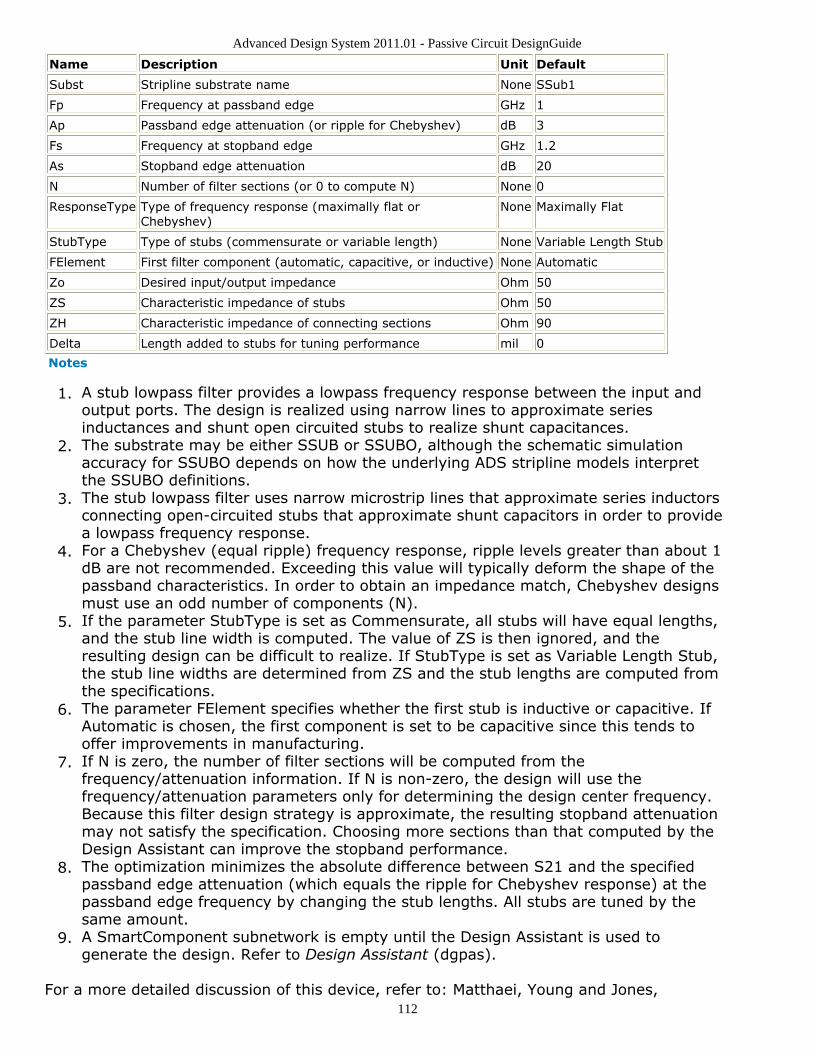
Advanced Design System 2011.01 - Passive Circuit DesignGuide
112
Name Description Unit Default
Subst Stripline substrate name None SSub1
Fp Frequency at passband edge GHz 1
Ap Passband edge attenuation (or ripple for Chebyshev) dB 3
Fs Frequency at stopband edge GHz 1.2
As Stopband edge attenuation dB 20
N Number of filter sections (or 0 to compute N) None 0
ResponseType Type of frequency response (maximally flat orChebyshev)
None Maximally Flat
StubType Type of stubs (commensurate or variable length) None Variable Length Stub
FElement First filter component (automatic, capacitive, or inductive) None Automatic
Zo Desired input/output impedance Ohm 50
ZS Characteristic impedance of stubs Ohm 50
ZH Characteristic impedance of connecting sections Ohm 90
Delta Length added to stubs for tuning performance mil 0
Notes
A stub lowpass filter provides a lowpass frequency response between the input and1.output ports. The design is realized using narrow lines to approximate seriesinductances and shunt open circuited stubs to realize shunt capacitances.The substrate may be either SSUB or SSUBO, although the schematic simulation2.accuracy for SSUBO depends on how the underlying ADS stripline models interpretthe SSUBO definitions.The stub lowpass filter uses narrow microstrip lines that approximate series inductors3.connecting open-circuited stubs that approximate shunt capacitors in order to providea lowpass frequency response.For a Chebyshev (equal ripple) frequency response, ripple levels greater than about 14.dB are not recommended. Exceeding this value will typically deform the shape of thepassband characteristics. In order to obtain an impedance match, Chebyshev designsmust use an odd number of components (N).If the parameter StubType is set as Commensurate, all stubs will have equal lengths,5.and the stub line width is computed. The value of ZS is then ignored, and theresulting design can be difficult to realize. If StubType is set as Variable Length Stub,the stub line widths are determined from ZS and the stub lengths are computed fromthe specifications.The parameter FElement specifies whether the first stub is inductive or capacitive. If6.Automatic is chosen, the first component is set to be capacitive since this tends tooffer improvements in manufacturing.If N is zero, the number of filter sections will be computed from the7.frequency/attenuation information. If N is non-zero, the design will use thefrequency/attenuation parameters only for determining the design center frequency.Because this filter design strategy is approximate, the resulting stopband attenuationmay not satisfy the specification. Choosing more sections than that computed by theDesign Assistant can improve the stopband performance.The optimization minimizes the absolute difference between S21 and the specified8.passband edge attenuation (which equals the ripple for Chebyshev response) at thepassband edge frequency by changing the stub lengths. All stubs are tuned by thesame amount.A SmartComponent subnetwork is empty until the Design Assistant is used to9.generate the design. Refer to Design Assistant (dgpas).
For a more detailed discussion of this device, refer to: Matthaei, Young and Jones,

Advanced Design System 2011.01 - Passive Circuit DesignGuide
113
Microwave Filters, Impedance-Matching Networks, and Coupling Structures, Artech House,1980, pp. 375.
Example
A stub lowpass filter was designed for a maximally flat response with a 3 dB attenuation atthe passband edge frequency of 1 GHz. A variable length StubType and automaticFElement resulted in 13 components for the design. Tuning using the OptimizationAssistant yielded a value of Delta = 174.401 mil.
SSRFilter (Stripline Stepped Impedance ResonatorFilter)
Symbol
Parameters
Advanced Design System 2011.01 - Passive Circuit DesignGuide
114
Name Description Unit Default
Subst Stripline substrate name None SSub1
Fs1 Lower stopband edge frequency GHz 1.8
Fp1 Lower passband edge frequency GHz 2
Fp2 Upper passband edge frequency GHz 2.2
Fs2 Lower stopband edge frequency GHz 2.4
Ap Passband edge attenuation (or ripple for Chebyshev) dB 3
As Stopband edge attenuation dB 20
N Number of filter sections (or 0 to compute N) None 0
ResponseType Type of frequency response (maximally flat orChebyshev)
None MaximallyFlat
Zo Desired input/output impedance Ohm 50
Fsp Center frequency of first spurious passband GHz 4.1
Delta Length added to filter sections for tuning performance mil 0
Notes
A stepped impedance resonator filter provides a bandpass frequency response1.between the input and output ports. N coupled-line sections produce an N−1 orderfilter response. Additional numbers of sections can be used to steepen the transitionband roll off or widen the pass bandwidth. The use on non-uniform impedance foreach resonator moves the second pass band center frequency away from the secondharmonic of the fundamental frequency.The substrate may be either SSUB or SSUBO, although the schematic simulation2.accuracy for SSUBO depends on how the underlying ADS stripline models interpretthe SSUBO definitions.Because of the heavy computational burden in determining the line parameters, a3.brief delay will occur for the design.For a Chebyshev (equal ripple) frequency response, ripple levels greater than about 14.dB are not recommended. Exceeding this value will typically deform the shape of thepassband characteristics.If N is zero, the number of filter sections will be computed from the5.frequency/attenuation information. If N is non-zero, the design will use thefrequency/attenuation parameters only for determining the design center frequency.The center frequency of the first spurious passband should be on the order of twice6.the fundamental passband center frequency.The optimization minimizes the absolute difference between S21 in dB and the7.specified passband edge attenuation (which equals the ripple for Chebyshevresponse) at the passband edge frequencies. Because only the line lengths arechanged, this tuning will typically center the response within the specified passband.More advanced shaping of the passband response can be accomplished by manuallytuning the widths and spacings of the coupled filter sections.A SmartComponent subnetwork is empty until the Design Assistant is used to8.generate the design. Refer to Design Assistant (dgpas).
For a more detailed discussion of this device, refer to: Makimoto and Yamashita,"Bandpass filters using parallel coupled stripline stepped impedance resonators," IEEETrans. Microwave Theory and Techniques , vol MTT-28, pp. 1413-1417, 1980.
Example
A stepped impedance resonator filter was designed for a maximally flat response with the3 dB passband edge frequencies at 2 GHz and 2.2 GHz respectively. The second passband
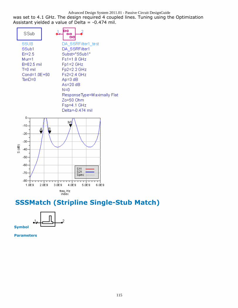
Advanced Design System 2011.01 - Passive Circuit DesignGuide
115
was set to 4.1 GHz. The design required 4 coupled lines. Tuning using the OptimizationAssistant yielded a value of Delta = -0.474 mil.
SSSMatch (Stripline Single-Stub Match)
Symbol
Parameters
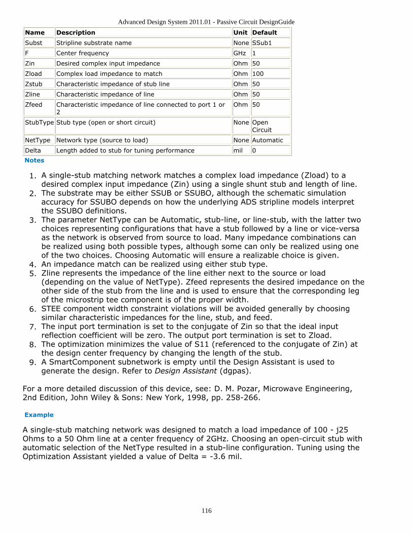
Advanced Design System 2011.01 - Passive Circuit DesignGuide
116
Name Description Unit Default
Subst Stripline substrate name None SSub1
F Center frequency GHz 1
Zin Desired complex input impedance Ohm 50
Zload Complex load impedance to match Ohm 100
Zstub Characteristic impedance of stub line Ohm 50
Zline Characteristic impedance of line Ohm 50
Zfeed Characteristic impedance of line connected to port 1 or2
Ohm 50
StubType Stub type (open or short circuit) None OpenCircuit
NetType Network type (source to load) None Automatic
Delta Length added to stub for tuning performance mil 0
Notes
A single-stub matching network matches a complex load impedance (Zload) to a1.desired complex input impedance (Zin) using a single shunt stub and length of line.The substrate may be either SSUB or SSUBO, although the schematic simulation2.accuracy for SSUBO depends on how the underlying ADS stripline models interpretthe SSUBO definitions.The parameter NetType can be Automatic, stub-line, or line-stub, with the latter two3.choices representing configurations that have a stub followed by a line or vice-versaas the network is observed from source to load. Many impedance combinations canbe realized using both possible types, although some can only be realized using oneof the two choices. Choosing Automatic will ensure a realizable choice is given.An impedance match can be realized using either stub type.4.Zline represents the impedance of the line either next to the source or load5.(depending on the value of NetType). Zfeed represents the desired impedance on theother side of the stub from the line and is used to ensure that the corresponding legof the microstrip tee component is of the proper width.STEE component width constraint violations will be avoided generally by choosing6.similar characteristic impedances for the line, stub, and feed.The input port termination is set to the conjugate of Zin so that the ideal input7.reflection coefficient will be zero. The output port termination is set to Zload.The optimization minimizes the value of S11 (referenced to the conjugate of Zin) at8.the design center frequency by changing the length of the stub.A SmartComponent subnetwork is empty until the Design Assistant is used to9.generate the design. Refer to Design Assistant (dgpas).
For a more detailed discussion of this device, see: D. M. Pozar, Microwave Engineering,2nd Edition, John Wiley & Sons: New York, 1998, pp. 258-266.
Example
A single-stub matching network was designed to match a load impedance of 100 - j25Ohms to a 50 Ohm line at a center frequency of 2GHz. Choosing an open-circuit stub withautomatic selection of the NetType resulted in a stub-line configuration. Tuning using theOptimization Assistant yielded a value of Delta = -3.6 mil.

Advanced Design System 2011.01 - Passive Circuit DesignGuide
117
STCoupler (Stripline Tee Power Divider)
Symbol
Parameters
Name Description Unit Default
Subst Strip substrate name None SSub1
F Center frequency GHz 1
Zo1 Characteristic impedance of input port 1 Ohm 50
Zo2 Characteristic impedance of output port 2 Ohm 50
Zo3 Characteristic impedance of output port 3 Ohm 50
K Ratio of power out port 2 to power out port 3 None 1.0
Delta Length added to quarter-wave sections for tuningperformance
mil 0
Notes
A tee power divider splits the power at the input (pin 1) between the two outputs1.(pins 2 and 3). Unequal or equal power splits can be realized. The input port will bematched to its feeding line, although in general the output ports will not be matched.The substrate may be either SSUB or SSUBO, although the schematic simulation2.accuracy for SSUBO depends on how the underlying ADS stripline models interpretthe SSUBO definitions.The value of K can be set to realize the desired power split out of ports 2 and 3.3.However, choosing K larger than 3 to 4 (or smaller than 1/3 to 1/4) can cause theratio of the widths of the tee branches to violate the range of the STEE simulationmodel. While the simulation will still proceed, the results can have some inaccuracies.Quarter-wave matching sections are provided on the output ports to ensure a proper4.power split is achieved.The optimization minimizes the input reflection coefficient (S11) at the design center5.frequency by changing the length of the quarter wave transformers on the outputlegs.A SmartComponent subnetwork is empty until the Design Assistant is used to6.generate the design. Refer to Design Assistant (dgpas).

Advanced Design System 2011.01 - Passive Circuit DesignGuide
118
For a more detailed discussion of this device, see: D. M. Pozar, Microwave Engineering,2nd Edition, John Wiley & Sons: New York, 1998, pp. 360-361.
Example
A tee power divider was designed for a center frequency of 1 GHz with an equal powersplit (K = 1). Tuning using the Optimization Assistant yielded a value of Delta = -24.228mil.
SWDCoupler (Stripline Wilkinson Divider)
Symbol
Parameters
Name Description Unit Default
Subst Strip substrate name None SSub1
F Center frequency GHz 1
DeltaF Frequency bandwidth GHz 0.5
Zo Characteristic impedance Ohm 50
ResponseType Type of frequency response None Uniform
N Number of quarter-wave sections; set N=0 to compute N None 0
Rmax Maximum voltage reflection coefficient on input port None 0.1
K Ratio of power out port 2 to power out port 3 None 1.0
Wgap Width of gap for resistor mil 50
Delta Length added to quarter-wave branches for tuning performance mil 0
Notes
A Wilkinson power divider splits the power at the input (pin 1) between the two1.outputs (pins 2 and 3). Unequal or equal power splits can be realized. The signals atthe outputs are in phase. All three ports will be matched, and ports 2 and 3 will ingeneral be well isolated from each other.The substrate may be either SSUB or SSUBO, although the schematic simulation2.accuracy for SSUBO depends on how the underlying ADS stripline models interpretthe SSUBO definitions.For broadband performance, the divider can have multiple quarter-wave sections. If3.

Advanced Design System 2011.01 - Passive Circuit DesignGuide
119
the number of sections N is set to zero, the Design Assistant chooses N such thatsuch that the reflection coefficient is less than Rmax over the bandwidth DeltaF(centered at the design center frequency). the resulting bandwidth can be broaderthan that specified. Otherwise, Rmax and DeltaF are ignored.ResponseType specifies the distribution of the partial reflection coefficients seen at4.each section interface - Uniform, Binomial, and Chebyshev distributions are available.These in turn specify the shape of the reflection coefficient versus frequency.For a single section divider (N=1), the value of K can be set to realize the desired5.power split out of ports 2 and 3. Be aware that choosing K larger than 3 to 4 (orsmaller than 1/3 to 1/4) is likely to cause difficulties in the design.Pozar specifies K2= P3/P2, while the DesignGuide uses K2= P2/P3. Therefore, if you6.use the equations in Pozar to verify everything, you must substitute 1/K for K. TheDesignGuide automatically puts quarter-wave matching sections on ports 2 and 3, soall ports are matched to the characteristic impedance. If you remove these matchingsegments, the output impedances are those specified by Pozar.The optimization minimizes the input reflection coefficient (S11) at the design center7.frequency by changing the length of the quarter wave branches forming the divider.A SmartComponent subnetwork is empty until the Design Assistant is used to8.generate the design. Refer to Design Assistant (dgpas).
For a more detailed discussion of this device, see: D. M. Pozar, Microwave Engineering,2nd Edition, John Wiley & Sons: New York, 1998, pp. 363-368.
Example
A single-section Wilkinson power divider (N=1) was designed for a center frequency of 5GHz with an equal power split (K=1) and a gap width for the resistor of 50 mil. Tuningusing the Optimization Assistant yielded a value of Delta = -32.834 mil.


