55
1 Multipaction, Corona and Passive Intermodulation in passive microwave components

1
Multipaction, Corona and Passive
Intermodulation in passive microwave components

2
Agenda
Mutlipaction
Corona (critical pressure)
Passive Intermodulation
3
Multipaction

4
• What is multipaction?
• What are requirements for multipaction?
• Some underlying physics
• Description of multipaction curves
• General procedure for analysis
• Examples
• Preventions
• Design Limitations and effects
• Testing and detection
OUTLINE
5
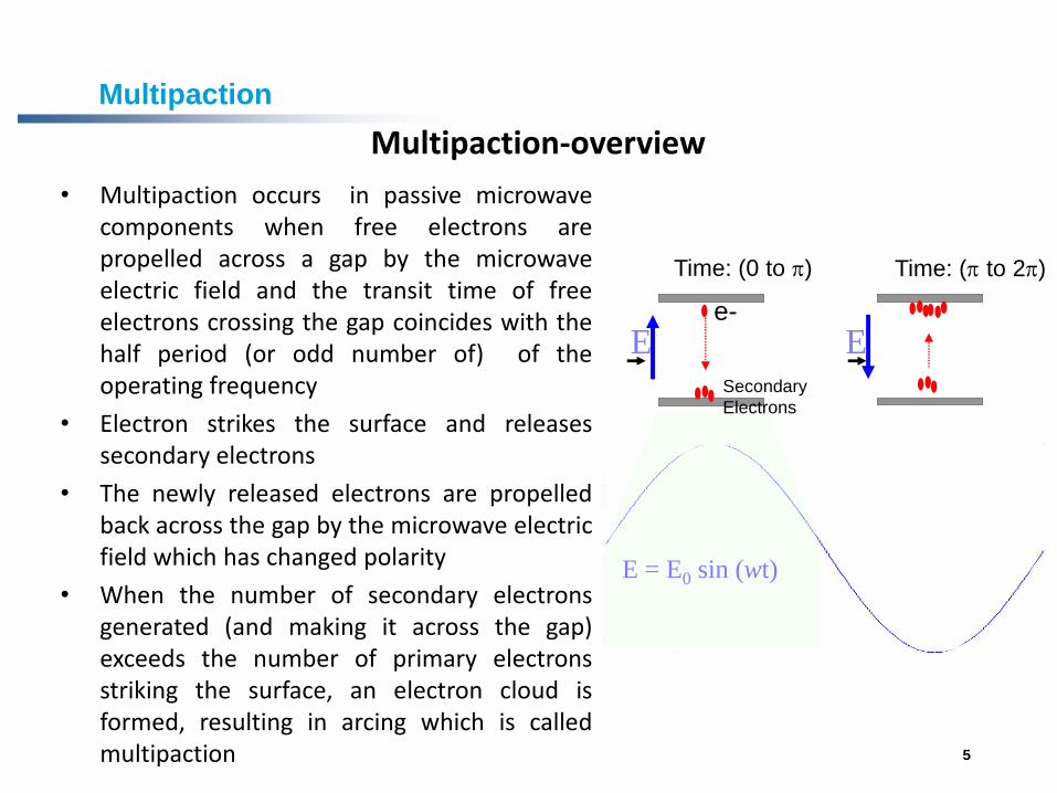
• Multipaction occurs in passive microwavecomponents when free electrons arepropelled across a gap by the microwaveelectric field and the transit time of freeelectrons crossing the gap coincides with thehalf period (or odd number of) of theoperating frequency
• Electron strikes the surface and releasessecondary electrons
• The newly released electrons are propelledback across the gap by the microwave electricfield which has changed polarity
• When the number of secondary electronsgenerated (and making it across the gap)exceeds the number of primary electronsstriking the surface, an electron cloud isformed, resulting in arcing which is calledmultipaction
Multipaction
Multipaction-overview
Time: (0 to ) Time: ( to 2)
e-
Secondary
Electrons
E E
E = E0 sin (wt)
6
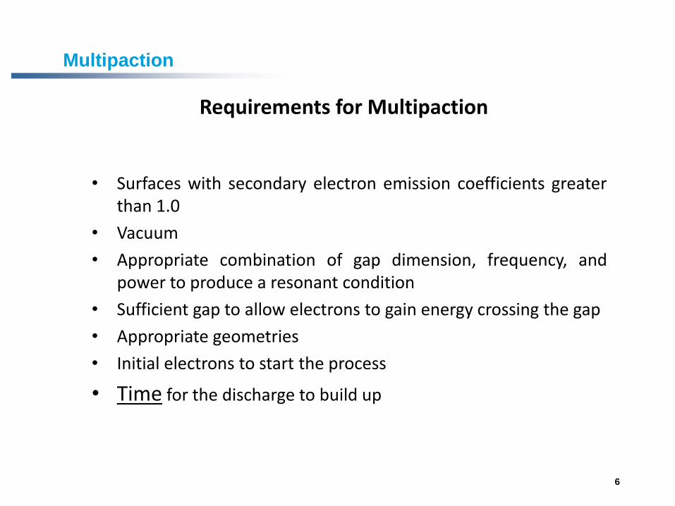
Requirements for Multipaction
• Surfaces with secondary electron emission coefficients greaterthan 1.0
• Vacuum
• Appropriate combination of gap dimension, frequency, andpower to produce a resonant condition
• Sufficient gap to allow electrons to gain energy crossing the gap
• Appropriate geometries
• Initial electrons to start the process
• Time for the discharge to build up
Multipaction
7
Time to Initiate Multipaction
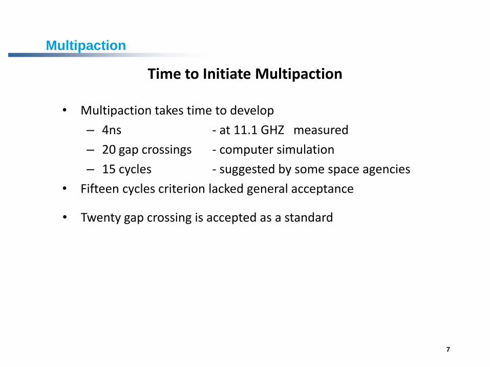
• Multipaction takes time to develop
– 4ns - at 11.1 GHZ measured
– 20 gap crossings - computer simulation
– 15 cycles - suggested by some space agencies
• Fifteen cycles criterion lacked general acceptance
Multipaction
• Twenty gap crossing is accepted as a standard

8
Electron Tracking
Multipaction has three stages
• Drift
– Due to initial velocity
– Oscillation due to field superimposed on motion
– Terminated by collision with wall (low energy, low yield)
• Synchronization
– Electrons travel out of step with applied field
– Some collisions productive; others not
• Build up
– Electrons in sync with applied field
– All collisions somewhat productive
Multipaction

9
Electron Emission - Yield
• Low energy electrons absorbed
• High energy electrons penetrate too deep – yield low
• Yield greater than one required for multipaction
Multipaction
10
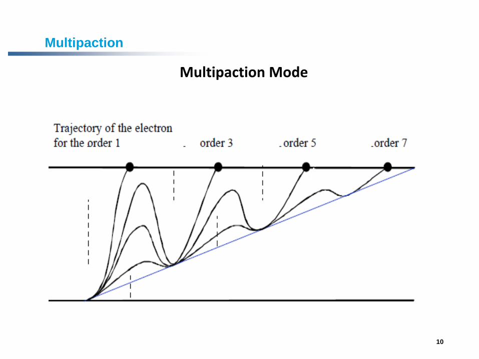
Multipaction Mode
Multipaction
11
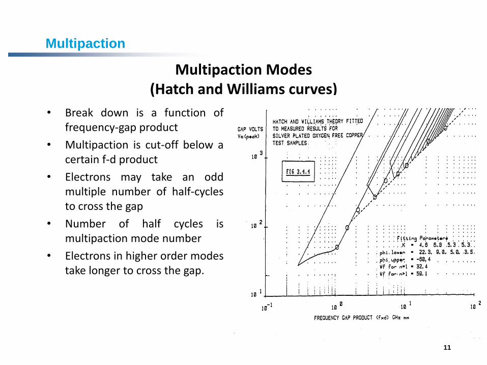
Multipaction Modes(Hatch and Williams curves)
• Break down is a function offrequency-gap product
• Multipaction is cut-off below acertain f-d product
• Electrons may take an oddmultiple number of half-cyclesto cross the gap
• Number of half cycles ismultipaction mode number
• Electrons in higher order modestake longer to cross the gap.
Multipaction

12
• Multipaction curves are a function of materials
• Curves are limited to four materials
• Multipaction does not happen below curve
Multipaction
Multipaction Modes(Susceptibility curves)

13
• Asymmetric modes3/2 cycle transit one way½ cycle transit other direction other wayNet energy gain each directionIntegral number of cycles for each round trip
• Hybrid modesAlternating between modes every round trip
Eg. 3 cycles, 4cycles, 3 cycles, 4cycles, 3 cycles, 4cycles
Transition between two modes
Multipaction Modes
Multipaction
14
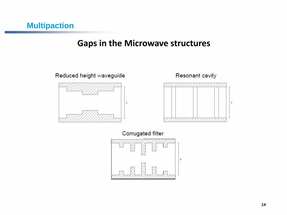
Gaps in the Microwave structures
Multipaction

15
General Analysis Procedure
1. Determine critical gaps
2. Make assumptions about surface materials if necessary
3. Calculate breakdown voltage from the curves
4. Relate voltage in breakdown region to power level
5. Calculate breakdown power
6. Calculate breakdown margin from the applied power
7. Consider geometry effects
Note: This is the worst case analysis procedure. Alternatively therealistic analysis can be conducted by adding voltage probes inthe critical gaps in the EM model(CST, HFSS) to calculate therealistic voltage across the gaps and then compare it to thebreakdown voltage from the curves.
Multipaction
16
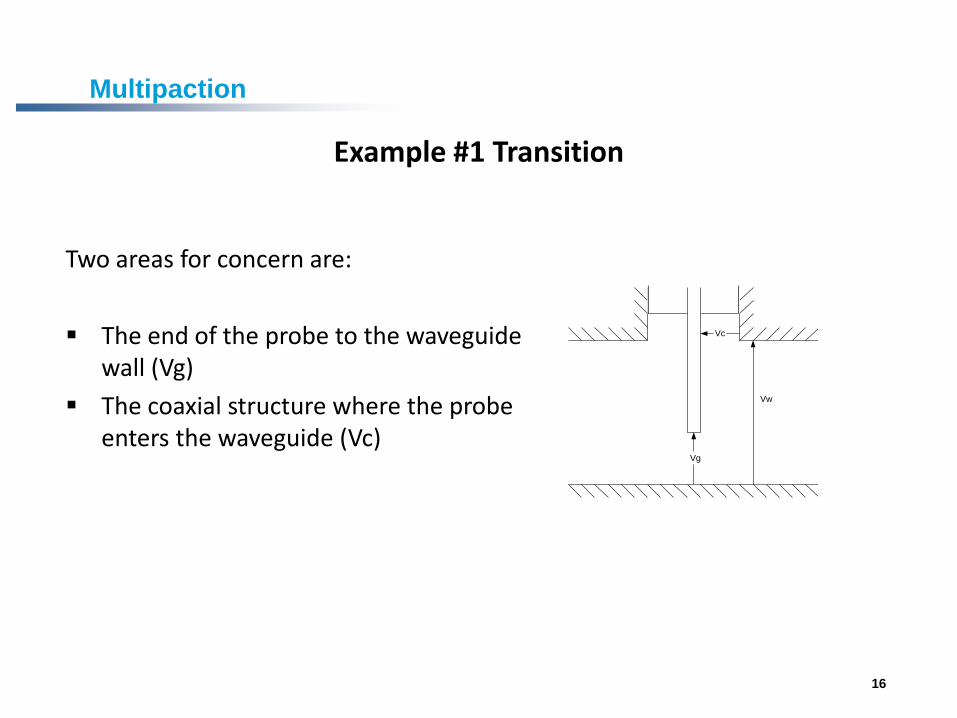
Example #1 Transition
Two areas for concern are:
The end of the probe to the waveguide wall (Vg)
The coaxial structure where the probe enters the waveguide (Vc)
Vg
Vw
Vc
Multipaction

17
Transition
Coaxial Structure
Hole diameter is .162 in. Centre conductor is .050 in.
gap = .056 in = 1.422 mm
@f = 10.95 GHz, fd = 15.57 GHz mm
For Ag/Au surface, breakdown voltage V = 981 V(from multipaction curves)
Pb = V2/2ZC = 9.62 kW (ZC = 50 )
Multipaction
18
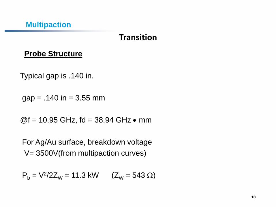
Transition
Probe Structure
Typical gap is .140 in.
gap = .140 in = 3.55 mm
@f = 10.95 GHz, fd = 38.94 GHz mm
For Ag/Au surface, breakdown voltage
V= 3500V(from multipaction curves)
Pb = V2/2ZW = 11.3 kW (ZW = 543 )
Multipaction
19
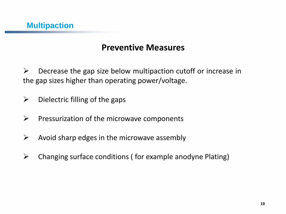
Preventive Measures
Decrease the gap size below multipaction cutoff or increase inthe gap sizes higher than operating power/voltage.
Dielectric filling of the gaps
Pressurization of the microwave components
Avoid sharp edges in the microwave assembly
Changing surface conditions ( for example anodyne Plating)
Multipaction

20
Design limitations due to multipaction
Limits on F*d implies limitations on the dimensions of theassembly
Dielectric filling can cause change in S parameters and thereby achange may be required in the dimensions of the assembly in orderto achieve the S-parameter spec.
Pressurization can increase the risk of corona and PIM
Change in surface conditions will imply change in S-parameters
Multipaction
21
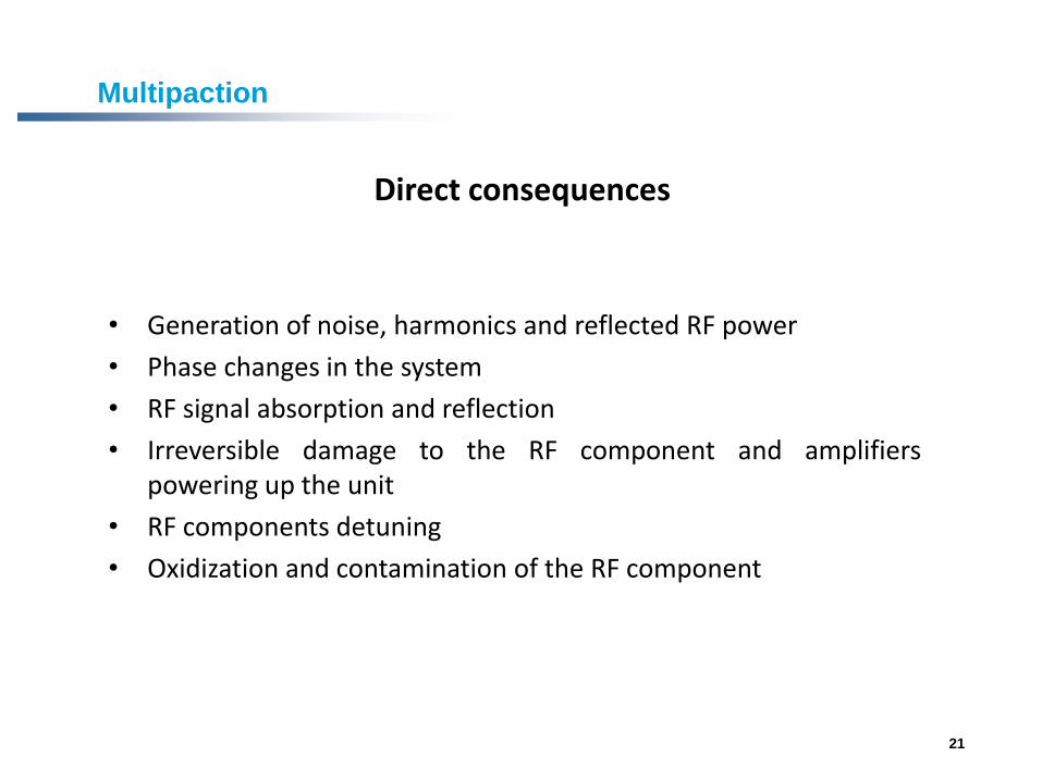
Direct consequences
• Generation of noise, harmonics and reflected RF power
• Phase changes in the system
• RF signal absorption and reflection
• Irreversible damage to the RF component and amplifierspowering up the unit
• RF components detuning
• Oxidization and contamination of the RF component
Multipaction

22
Detection methods
• Local:
– Electron probes
– fibre optic
– Mass spectrometer
• Global :
– nulling
– Harmonics
– Near band noise
Multipaction
23
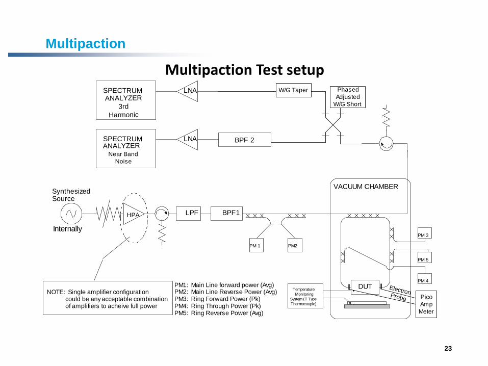
Multipaction Test setup
LPF BPF1
DUTTemperature
Monitoring
System (T Type
Thermocouple)
PM2PM 1
PM 3
PM 5
PM 4
VACUUM CHAMBER
HPA
SynthesizedSource
Internally
NOTE: Single amplifier configuration could be any acceptable combination of amplifiers to acheive full power
PM1: Main Line forward power (Avg)PM2: Main Line Reverse Power (Avg)PM3: Ring Forward Power (Pk)PM4: Ring Through Power (Pk)PM5: Ring Reverse Power (Avg)
BPF 2LNASPECTRUMANALYZER
Near Band
Noise
LNASPECTRUMANALYZER
3rd
Harmonic
W/G Taper Phased
Adjusted
W/G Short
ElectronProbe Pico
Amp
Meter
Multipaction
24
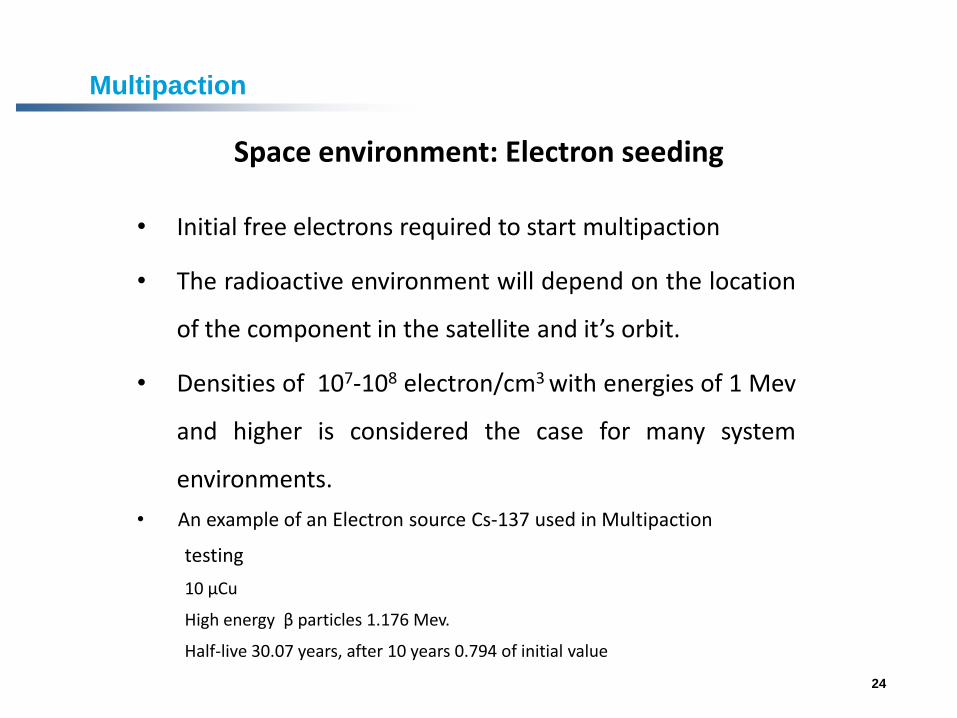
Space environment: Electron seeding
• Initial free electrons required to start multipaction
• The radioactive environment will depend on the location
of the component in the satellite and it’s orbit.
• Densities of 107-108 electron/cm3 with energies of 1 Mev
and higher is considered the case for many system
environments.
• An example of an Electron source Cs-137 used in Multipaction
testing
10 μCu
High energy β particles 1.176 Mev.
Half-live 30.07 years, after 10 years 0.794 of initial value
Multipaction
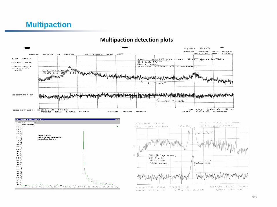
25
Multipaction detection plots
Multipaction
26
Multipaction
• RF breakdown phenomena
• Takes place under vacuum conditions only.
• Requires the presence of high electrical fields between surfaces
• Free electrons accelerated by RF voltage to create an electron resonance growth.
•The breakdown level is affected by:
- internal geometry (gap size)
- operating frequency
- applied RF voltage
- surface conditions
Time: (0 to ) Time: ( to 2)
e-
Secondary
Electrons
E E
E = E0 sin (wt)
• Results of the RF breakdown:
- disruption or loss of signal
- permanent damage to component
27
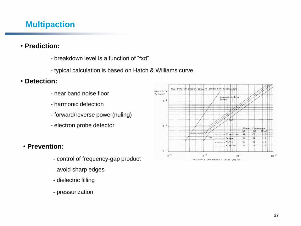
Multipaction
• Prediction:
- breakdown level is a function of “fxd”
- typical calculation is based on Hatch & Williams curve
• Prevention:
- control of frequency-gap product
- avoid sharp edges
- dielectric filling
- pressurization
• Detection:
- near band noise floor
- harmonic detection
- forward/reverse power(nuling)
- electron probe detector
28
Corona
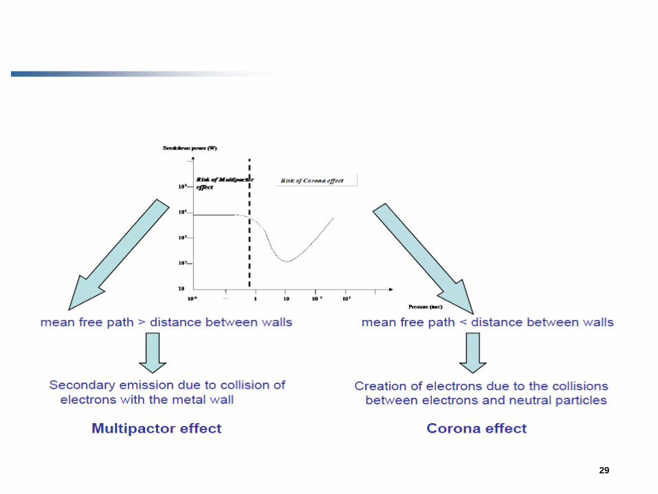
29
30
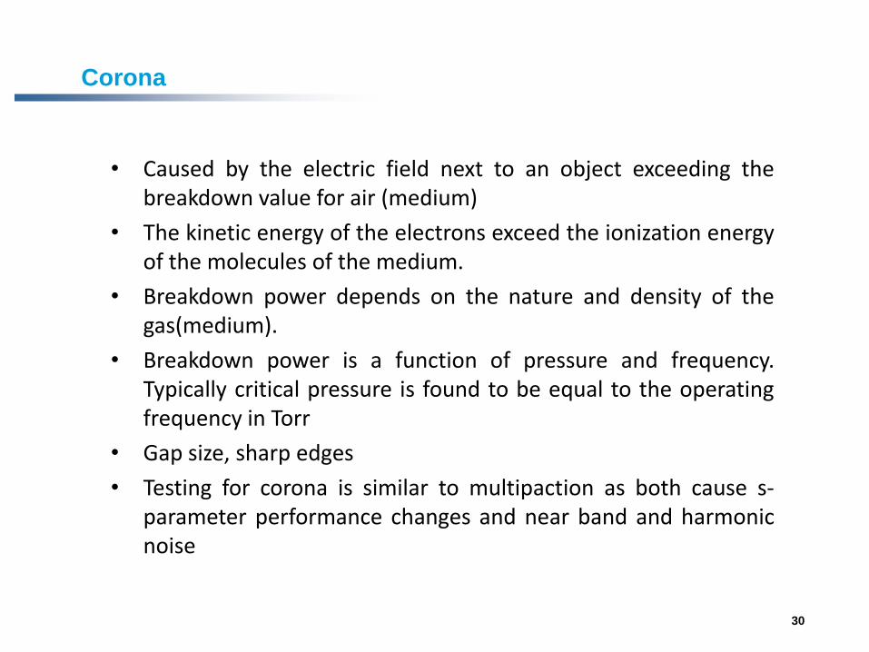
• Caused by the electric field next to an object exceeding thebreakdown value for air (medium)
• The kinetic energy of the electrons exceed the ionization energyof the molecules of the medium.
• Breakdown power depends on the nature and density of thegas(medium).
• Breakdown power is a function of pressure and frequency.Typically critical pressure is found to be equal to the operatingfrequency in Torr
• Gap size, sharp edges
• Testing for corona is similar to multipaction as both cause s-parameter performance changes and near band and harmonicnoise
Corona

31
• The voltage at which a spark occurs (known as breakdown voltage) is dependent on the product of air pressure (P) and the separation between the electrodes (d).
• Microwave frequencies alter characteristics
Paschen’s Law
Corona
32
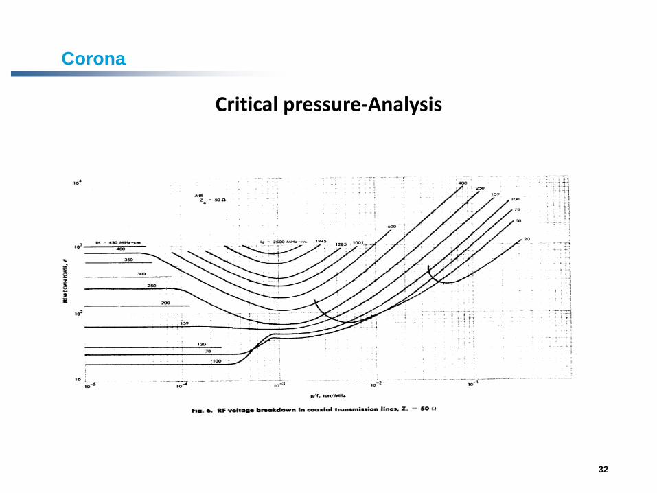
Critical pressure-Analysis
Corona

33
Preventive Measures
Reduce Gap voltage
Dielectric filling of the gaps
Avoid sharp edges
PressurizationCavity/Resonator Lid
Corona
34
Passive IntermodulationPIM
(A multidisciplinary problem)
35
Outline
• Introduction
• General review
• PIM Sources
• Design examples
– Waveguide
– Coaxial
• Design Rules / Aspects to consider
• PIM testing
Passive Intermodulation

36
Introduction
• Passive Intermodulation (PIM ) is a non linear behaviour that generates “noise”at frequencies which are linear combinations of the input carriers.
• The amplitude of the signal created needs to be typically 170 dBc below thetransmit signals ( ~1x10⁻⁹ mW) . If higher, it may interfere with the receive signal.
• Good performance needs to be proven over the satellite operating temperaturein space.
• PIM is not only generated within the microwave components. It can also becreated at other locations of the satellite that may be exposed to electricalcurrents e.g. reflectors, thermal banquets. Spacecraft level testing becomes verycomplex.
• Payloads where the antenna is used to transmit and receive require especialattention to passive intermodulation products generation
Passive Intermodulation
37
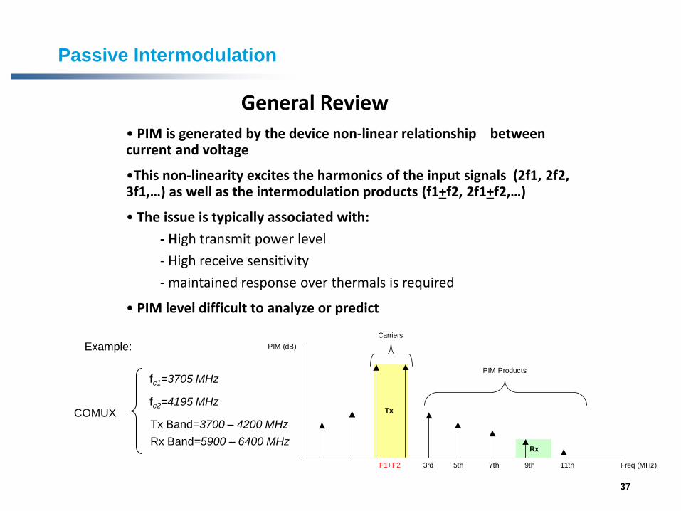
General Review
• PIM is generated by the device non-linear relationship between current and voltage
•This non-linearity excites the harmonics of the input signals (2f1, 2f2, 3f1,…) as well as the intermodulation products (f1+f2, 2f1+f2,…)
• The issue is typically associated with:
- High transmit power level
- High receive sensitivity
- maintained response over thermals is required
• PIM level difficult to analyze or predict
Example:
fc1=3705 MHz
fc2=4195 MHz
Tx Band=3700 – 4200 MHz
Rx Band=5900 – 6400 MHz
COMUX
F1+F2 3rd 5th 7th 9th 11th
Tx
Rx
Carriers
PIM Products
PIM (dB)
Freq (MHz)
Passive Intermodulation
38
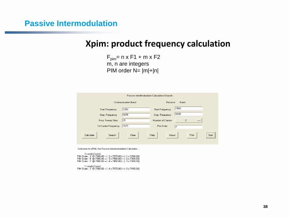
Xpim: product frequency calculation
Fpim= n x F1 + m x F2
m, n are integers
PIM order N= |m|+|n|
Passive Intermodulation
39
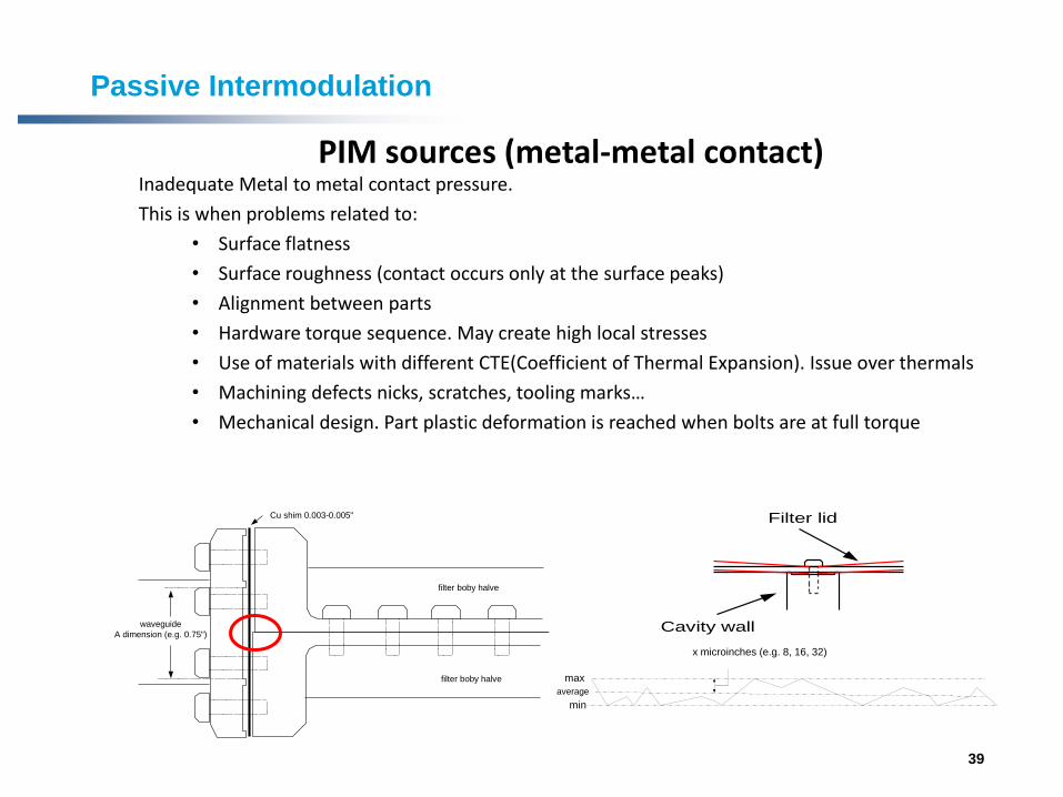
PIM sources (metal-metal contact)Inadequate Metal to metal contact pressure.
This is when problems related to:
• Surface flatness
• Surface roughness (contact occurs only at the surface peaks)
• Alignment between parts
• Hardware torque sequence. May create high local stresses
• Use of materials with different CTE(Coefficient of Thermal Expansion). Issue over thermals
• Machining defects nicks, scratches, tooling marks…
• Mechanical design. Part plastic deformation is reached when bolts are at full torque
average
min
max
x microinches (e.g. 8, 16, 32)
filter boby halve
filter boby halve
waveguide
A dimension (e.g. 0.75")
Cu shim 0.003-0.005"
Cavity wall
Filter lid
Passive Intermodulation
40
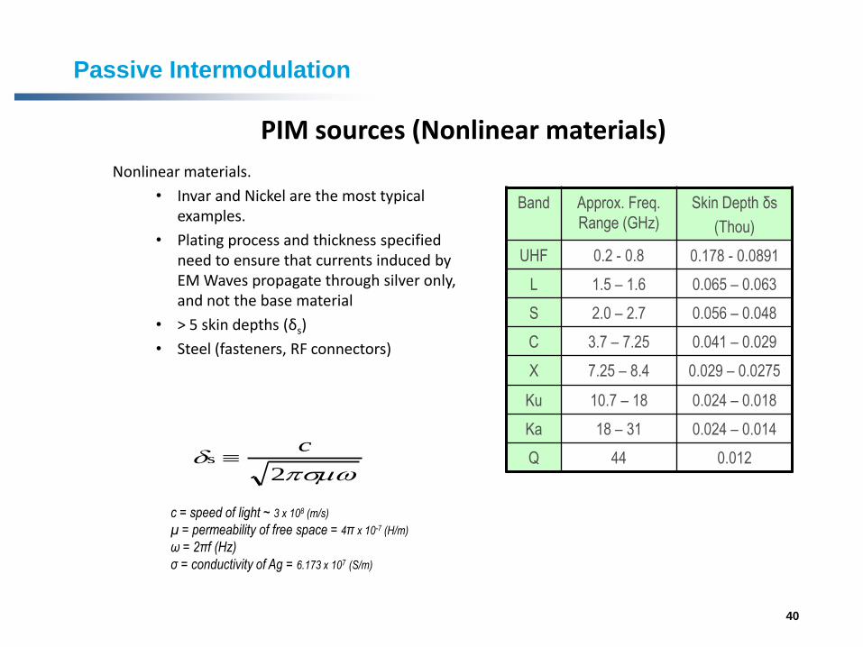
PIM sources (Nonlinear materials)
Nonlinear materials.
• Invar and Nickel are the most typical examples.
• Plating process and thickness specified need to ensure that currents induced by EM Waves propagate through silver only, and not the base material
• > 5 skin depths (δs)
• Steel (fasteners, RF connectors)
2s
c
c = speed of light ~ 3 x 10⁸ (m/s)
μ = permeability of free space = 4π x 10-7 (H/m)
ω = 2πf (Hz)
σ = conductivity of Ag = 6.173 x 10⁷ (S/m)
Band Approx. Freq.
Range (GHz)
Skin Depth δs
(Thou)
UHF 0.2 - 0.8 0.178 - 0.0891
L 1.5 – 1.6 0.065 – 0.063
S 2.0 – 2.7 0.056 – 0.048
C 3.7 – 7.25 0.041 – 0.029
X 7.25 – 8.4 0.029 – 0.0275
Ku 10.7 – 18 0.024 – 0.018
Ka 18 – 31 0.024 – 0.014
Q 44 0.012
Passive Intermodulation

41
PIM sources
– Tuning screws
• They are located at high fields and currents regions to allow tunability, contact issue remain betweenscrew and filter body
– Poor solder joints
• If some flux residue (non linear material) is left after cleaning operation
– Solder joints under high stress
• Joint may crack creating a contact problem
– Contamination
• Minute metal particle from helical coils, bolts
• Any other material
– Micro cracks
• When semi rigid cables are bent, it may originate a crack on the internal or external conductors
Passive Intermodulation

42
PIM signal amplitude calculation
PIM & log (PN)
P = input power
N= order (e.g. 3)
• The lower the order of the product the stronger is expected its presence.
• General rule is that the amplitude of the PIM signal is proportional to the amplitude
of each carrier.
– It can be applied when the source is non linear materials
– It is in general wrong when the PIM source is metal to metal contacts (due to
mechanical stresses over thermals)
– Not valid at very high powers, PIM generation tend to saturate
-142
-141.5
-141
-140.5
-140
-139.5
-139
-138.5
-138
20 40 60 80 100 120 140
-145+log10(P**3)
PIM (dBm)
P(W)
Equal power applied
at F1 and F2
Passive Intermodulation
43
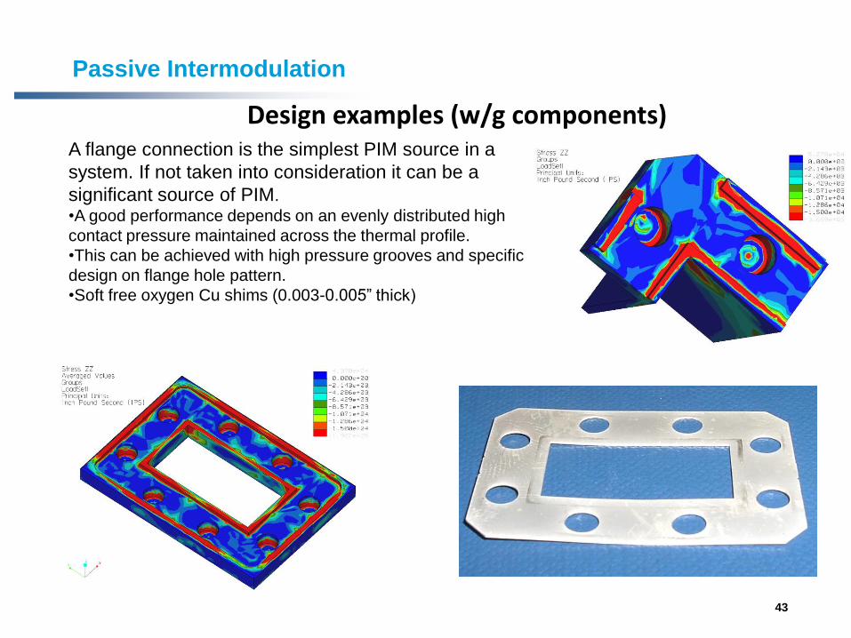
Design examples (w/g components)A flange connection is the simplest PIM source in a
system. If not taken into consideration it can be a
significant source of PIM.
•A good performance depends on an evenly distributed high
contact pressure maintained across the thermal profile.
•This can be achieved with high pressure grooves and specific
design on flange hole pattern.
•Soft free oxygen Cu shims (0.003-0.005” thick)
Passive Intermodulation

44
Design examples (w/g components to reject PIM)
Sicral 1B X-band OMUX ASSY
-160.00
-140.00
-120.00
-100.00
-80.00
-60.00
-40.00
-20.00
0.00
70
00
70
60
71
20
71
80
72
40
73
00
73
60
74
20
74
80
75
40
76
00
76
60
77
20
77
80
78
40
79
00
79
60
80
25
80
85
81
46
82
06
82
66
83
27
83
87
84
47
85
08
85
68
86
28
86
88
87
49
88
09
88
69
89
30
89
90
Frequency
Iso
lati
on
(d
B)
S11 MUX
S12 CH1
S12 CH2
S12 CH3
S12 CH4
S12 cover filter
S11 cover filter
4 Ch OMUX with an output cover filter. Channel filters are TE112 and cover filter is 10-2 TE101 rectangular cavity that provides at least 45 dB isolation. The passive Intermodulation generated mainly at manifold and interconnecting waveguide flanges is rejected by the output filter.
Rx-band
Passive Intermodulation
45
Design examples (w/g components to reject PIM)
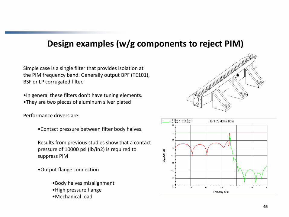
Simple case is a single filter that provides isolation at the PIM frequency band. Generally output BPF (TE101), BSF or LP corrugated filter.
•In general these filters don’t have tuning elements.•They are two pieces of aluminum silver plated
Performance drivers are:
•Contact pressure between filter body halves.
Results from previous studies show that a contact pressure of 10000 psi (lb/in2) is required to suppress PIM
•Output flange connection
•Body halves misalignment•High pressure flange•Mechanical load
46
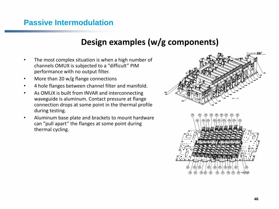
Design examples (w/g components)
• The most complex situation is when a high number of channels OMUX is subjected to a “difficult” PIM performance with no output filter.
• More than 20 w/g flange connections
• 4 hole flanges between channel filter and manifold.
• As OMUX is built from INVAR and interconnecting waveguide is aluminum. Contact pressure at flange connection drops at some point in the thermal profile during testing.
• Aluminum base plate and brackets to mount hardware can “pull apart” the flanges at some point during thermal cycling.
Passive Intermodulation

47
Design examples (coaxial assemblies)
Antenna
Connection J3
Transmit Path J1
Receive Path J2
The problem for coaxial devices becomes much more complex.
– Together with the same issues in waveguide, many other are encountered
– As the frequency is lower skin depth effects, defects on the surface like scratches, silver plating problems will be highlighted during testing.
– Contacts at tuning element become more problematic
– Dielectrics needed to support the striplines or present for other High Power problems may apply stress reducing contact pressure
– Connections of components and connectors became complex
• Solder joints are needed
• Connectors present contact issues and in general have a poor performance unless specifically developed and built for this purpose
Passive Intermodulation
48
Design Rules (Electrical)
• When possible (in complex assemblies) review the possibility of having an output filter with known good PIM performance by design. This filter would reduce the PIM level enough to make things easier for other components in assembly mainly during manufacturing and assembly.
• Realize electrical dimensions (e.g. couplings, tuning,…) in a way that mechanical contacts and assembly integration is easier.
• Take into account degradation at contacts between materials with different CTE (e.g. invar-aluminum)
• Ensure adequate thickness of silver layer in drawing. As the frequency is lower this becomes more important. S-band, L-Band, UHF
• Whenever possible avoid tuning elements
• If possible have contact joints in locations where current is low
Passive Intermodulation
49
Design Rules (Mechanical)
• Contact grooves, sufficient mounting hardware and configuration to have pressure across the thermal profile
– Filter body halves
– Flanges
– Filter body and lid
– Resonators and filter body
– …
• Avoid deformation of the mating surfaces, structural design needs to consider it (e.g. flanges with adequate thickness).
• Reduce the number of joints
• Avoid non linear materials (e.g. use of BeCu screws to support resonators instead of steel).
Passive Intermodulation

50
Testing: set-up layout
location of
DUT input
interface
hot plate
BPF(F
2)
BPF(F
2)
BPF(F
1)
Cover filter
BB
to isolatate
PIM
BPF\LPF
existing in
lab
(to reduce
the noise)
Al
SA
Dete
ctio
n
dip
lexe
r
Al
Al
H-plane
bend
Brackets
Baseplate not bolted if
possible (use weights)
Cover filter BB
DUT
Cover filter BB
Input filter
DUT has
vertical w/g
input
(circulator)
Al
hot plate
BPF
BPF/ LPF filter
existing from
current X-band
set-up!
Al
BPF
SA
Detection
diplexer
Al
Al
Cover filter BB
Set-up validation is required prior formal
test:
•Detection system works properly
•Set-up meets 5 dB better than
required specification
Set-up adequate PIM
performance validation
Example of configuration
during formal test.
DUT is a 2 channel MUX
with output cover filter
Passive Intermodulation
51
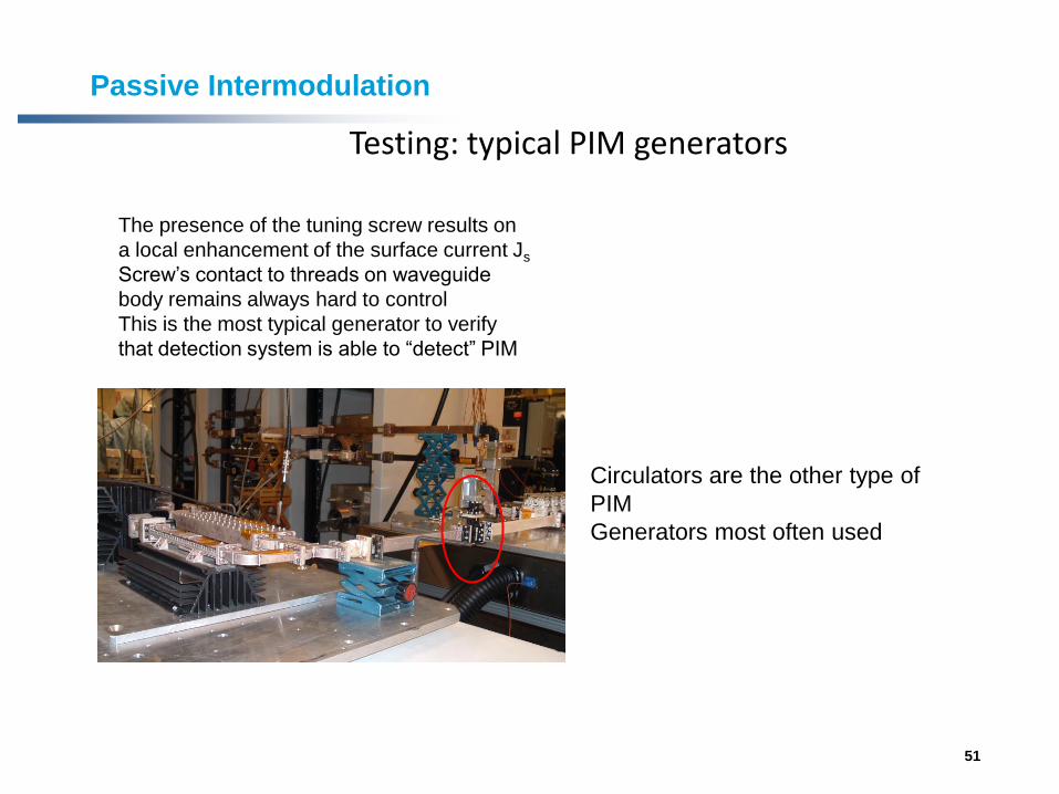
Testing: typical PIM generators
The presence of the tuning screw results on
a local enhancement of the surface current Js
Screw’s contact to threads on waveguide
body remains always hard to control
This is the most typical generator to verify
that detection system is able to “detect” PIM
Circulators are the other type of
PIM
Generators most often used
Passive Intermodulation

52
Test summary report
PIM detect PIM free DUT PIM measured
Passive Intermodulation
53
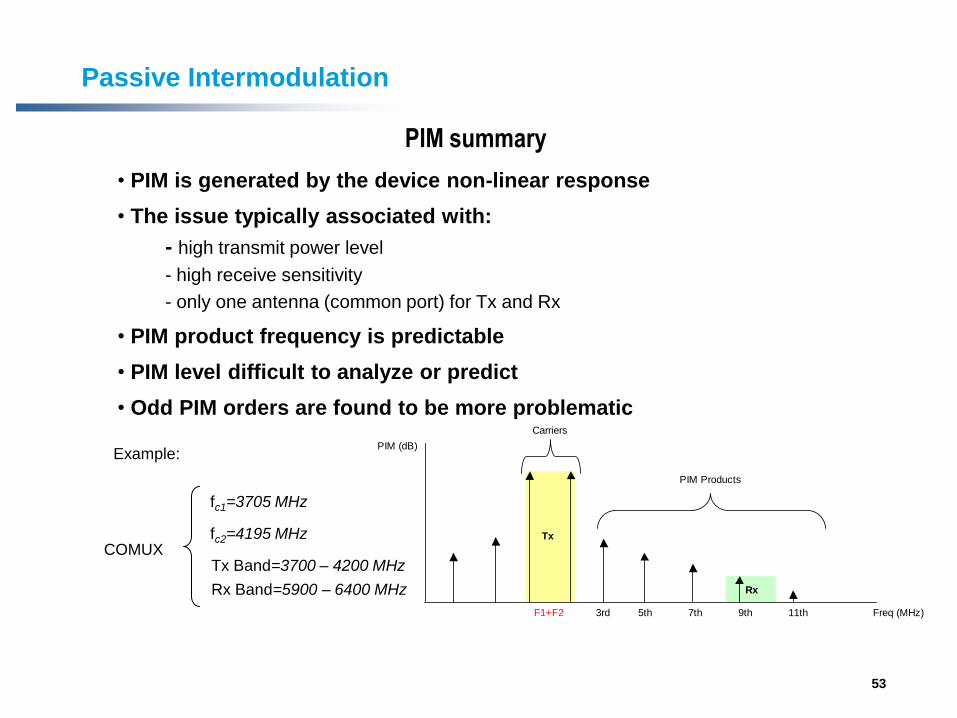
Passive Intermodulation
PIM summary
• PIM is generated by the device non-linear response
• The issue typically associated with:
- high transmit power level
- high receive sensitivity
- only one antenna (common port) for Tx and Rx
• PIM product frequency is predictable
• PIM level difficult to analyze or predict
• Odd PIM orders are found to be more problematic
Example:
fc1=3705 MHz
fc2=4195 MHz
Tx Band=3700 – 4200 MHz
Rx Band=5900 – 6400 MHz
COMUX
F1+F2 3rd 5th 7th 9th 11th
Tx
Rx
Carriers
PIM Products
PIM (dB)
Freq (MHz)

54
Passive Intermodulation
• Dominant contributors of non-linearity(for passive device):
- similar or dissimilar metal-to-metal joints
- poor mechanical contact
- poor surface finish
- high current density
- temperature variation
- magnetic non-linear effects
Simple design rules to reduce PIM level:
- limit the number of parts in the current path
- ensure adequate contact pressure
- smooth surface finish for connecting parts
- eliminate contaminants in the current path
- adequate and uniform plating thickness
- avoid magnetic materials in the current-carrying-path

55
Thank You


