22
Paul Feeney Semicon West 2011 US CMPUG Seminar F P R k il F eeneyP@Rock etmail.com

Outline
S i d t BEOL d FEOL di ti Semiconductor BEOL and FEOL directions
Semiconductor BEOL and FEOL planarization papplications
Expanding number of applications and steps Expanding number of applications and steps
Summaryy
Source: ITRS 2009
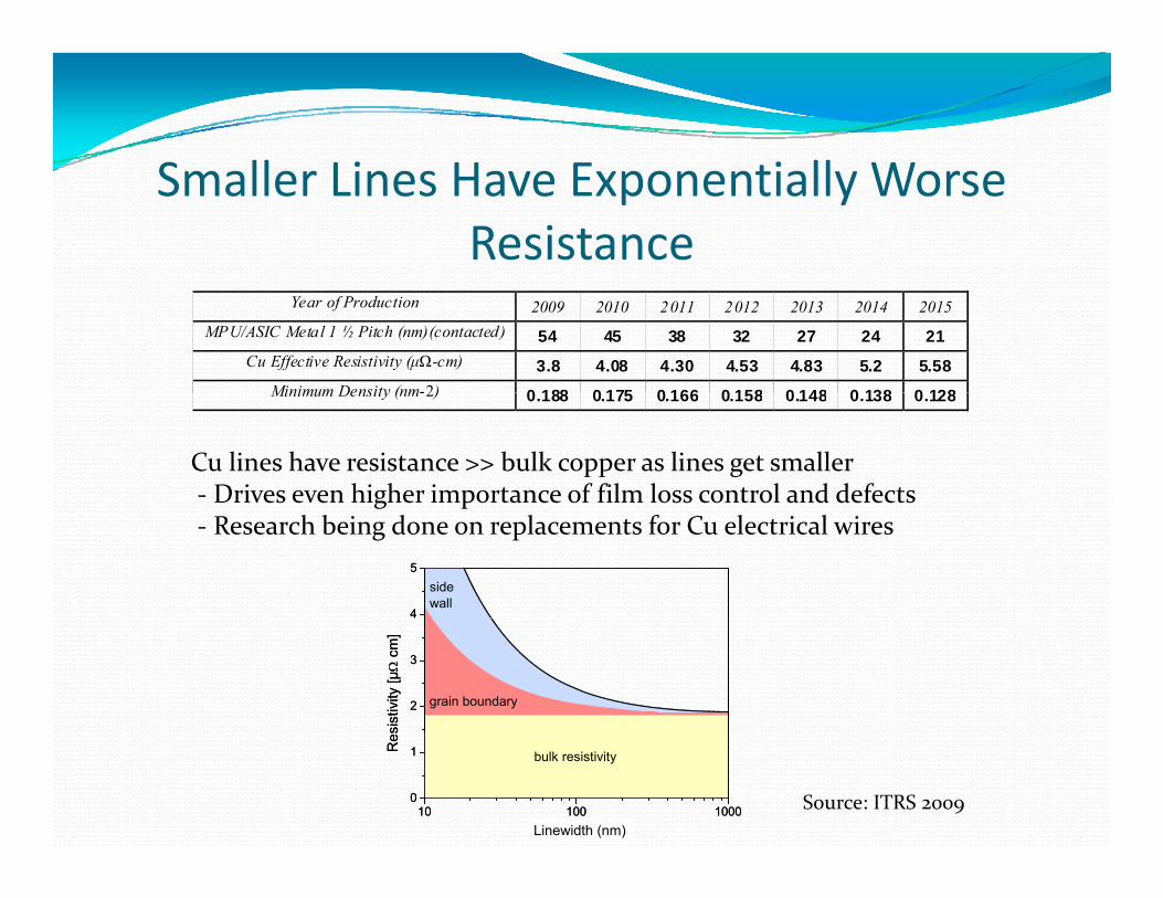
S ll Li H E ti ll WSmaller Lines Have Exponentially Worse Resistance
Year of Production 2009 2010 2011 2012 2013 2014 2015 MPU/ASIC Metal 1 ½ Pitch (nm)(contacted) 54 45 38 32 27 24 21
Cu Effective Resistivity (μΩ-cm) 3.8 4.08 4.30 4.53 4.83 5.2 5.58 Minimum Density (nm-2) 0 188 0 175 0 166 0 158 0 148 0 138 0 128Minimum Density (nm-2) 0.188 0.175 0.166 0.158 0.148 0.138 0.128
Cu lines have resistance >> bulk copper as lines get smaller‐ Drives even higher importance of film loss control and defectsg p‐ Research being done on replacements for Cu electrical wires
4
5sidewall
4
5sidewall
2
3
grain boundary
sist
ivity
[µ
cm
]
2
3
grain boundary
sist
ivity
[µ
cm
]
10 100 10000
1 bulk resistivity
Res
Line width [nm]Linewidth (nm)10 100 1000
0
1 bulk resistivity
Res
Line width [nm]Linewidth (nm)
Source: ITRS 2009

2010 Barrier/Nucleation/Resistivityf dYear of Production 2010 2011 2012 2013 2014 2015
MPU/ASIC Metal 1 ½ Pitch (nm)(contacted) 45 38 32 27 24 21
Barrier cladding thickness 3 3 2 9 2 6 2 4 2 1 1 9gMetal 1 (nm) 3.3 2.9 2.6 2.4 2.1 1.9
Conductor effective resistivity (µΩ-cm) Cu Metal 1 4.08 4.30 4.53 4.83 5.2 5.58
Year of Production 2016 2017 2018 2019 2020 2021 2022 2023 2024
MPU/ASIC Metal 1 ½ Pitch (nm)(contacted)
18.9 16.9 15.0 13.4 11.9 10.6 9.5 8.4 7.5
B i l ddi thi kBarrier cladding thickness Metal 1 (nm) 1.7 1.5 1.3` 1.2 1.1 1.0 0.9 0.8 0.7
Conductor effective resistivity (µΩ-cm) Cu Metal 1 6.01 6.33 6.7 7.34 8.19 8.51 9.84 11.30 12.91
• ALD barrier processes and metal capping layers for Cu are lagging in introduction – key challenge
• Resistivity increases due to scattering and impact of liners
ITRS 2010 Summer Conference – 14 July 2010 San Francisco, CA - 5 -
Resistivity increases due to scattering and impact of liners•No known practical solutions
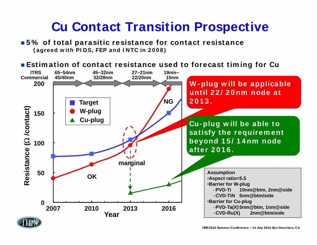
Cu Contact Transition Prospective5% of total parasitic resistance for contact resistance p
(agreed with PIDS, FEP and INTC in 2008)
Estimation of contact resistance used to forecast timing for Cu45/40 32/28 22/20 1565~54nm 45~32nm 27~21nm 19nm~ITRS
C i l
Target
45/40nm 32/28nm 22/20nmW-plug will be applicable until 22/20nm node at 2013.
200
)
15nm
NG
Commercial
W-plugCu-plug Cu-plug will be able to
satisfy the requirement b d / d
150
/con
tact
)
marginal
beyond 15/14nm node after 2016.
100
stan
ce (
OK50
Res
is Assumption•Aspect ratio=5.5•Barrier for W-plug
PVD-Ti 10nm@btm, 2nm@sideCVD-TiN 5nm@btm/side
B i f C l
ITRS 2010 Summer Conference – 14 July 2010 San Francisco, CA
02007 2010 2013 2016
Year
•Barrier for Cu-plugPVD-Ta(X) 5nm@btm, 1nm@sideCVD-Ru(X) 2nm@btm/side
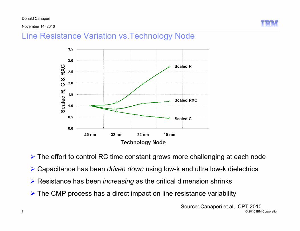
Line Resistance Variation vs.Technology Node
Donald Canaperi
November 14, 2010
The effort to control RC time constant grows more challenging at each nodeg g g
Capacitance has been driven down using low-k and ultra low-k dielectrics
Resistance has been increasing as the critical dimension shrinks
© 2010 IBM Corporation7
The CMP process has a direct impact on line resistance variability
Source: Canaperi et al, ICPT 2010

2010 Low k or nothing?Year of Production 2010 2011 2012 2013 2014 2015
MPU/ASIC Metal 1 ½ Pitch (nm)(contacted)
45 38 32 27 24 21
Interlevel metal insulator –bulk dielectric constant (κ) 2.3-2.5 2.3-2.5 2.3-2.5 2.1-2.3 2.1-2.3 2.1-2.3
Year of Production 2016 2017 2018 2019 2020 2021 2022 2023 2024
MPU/ASIC Metal 1 ½ Pitch (nm)(contacted)
18.9 16.9 15.0 13.4 11.9 10.6 9.5 8.4 7.5
Interlevel metal insulator –b lk di l t i t t ( ) 1.9–2.1 1.9–2.1 1.9–2.1 1.7–1.9 1.7–1.9 1.7–1.9 1.5–1.7 1.5–1.7 1.5–1.7
Air gap architectures will be required for bulk <2.0•No viable materials expected to be available.
bulk dielectric constant (κ)
No viable materials expected to be available.•Mechanical requirements easier to achieve with air-gaps.•End of the material solution and the beginning of an architecture solution
ITRS 2010 Summer Conference – 14 July 2010 San Francisco, CA - 8 -
architecture solution.
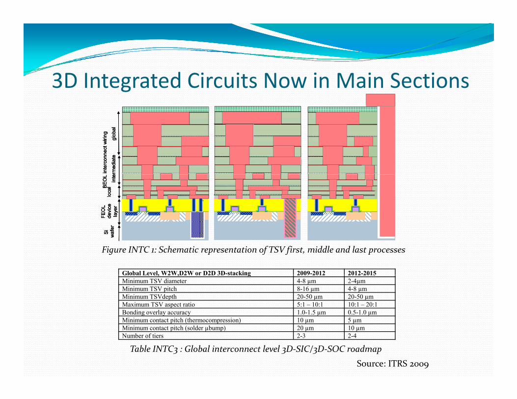
3D I d Ci i N i M i S i3D Integrated Circuits Now in Main Sectionsin
terc
onne
ct w
iring
rmed
iate
glob
al
inte
rcon
nect
wiri
ng
rmed
iate
glob
al
inte
rcon
nect
wiri
ng
rmed
iate
glob
allo
calBE
OL
inte
FEO
Lde
vice
laye
rlo
calBE
OL
inte
FEO
Lde
vice
laye
rlo
calBE
OL
inte
FEO
Lde
vice
laye
r
Si
waf
erSi
w
afer
Si
waf
er
Figure INTC 1: Schematic representation of TSV first, middle and last processes
Global Level, W2W,D2W or D2D 3D-stacking 2009-2012 2012-2015Global Level, W2W,D2W or D2D 3D stacking 2009 2012 2012 2015Minimum TSV diameter 4-8 µm 2-4µmMinimum TSV pitch 8-16 µm 4-8 µmMinimum TSVdepth 20-50 µm 20-50 µmMaximum TSV aspect ratio 5:1 – 10:1 10:1 – 20:1Bonding overlay accuracy 1.0-1.5 µm 0.5-1.0 µmMinimum contact pitch (thermocompression) 10 µm 5 µmMinimum contact pitch (solder µbump) 20 µm 10 µmNumber of tiers 2-3 2-4
Table INTC3 : Global interconnect level 3D‐SIC/3D‐SOC roadmap
Source: ITRS 2009

1st Generation HKMG: 45nmMC
AlW
NMOS PMOSSiGe
SiGe S/D integration for PMOS only
HfO2 based high‐k material for gate oxide
Source: IEDM 2009
O2 based g ate a o gate o de
3 ILD layers with nitride stress liner
Single W contact process
POP and Al CMP applicationsSource: Feeney et al, Taiwan CMPUG 2010

Cu Ta
2nd Generation HKMG: 32nm
Al
MC
M0
NMOS PMOS SiGe
MC
SiC?
Raised S/D for NMOS with SiGe for PMOS
Extended high k surrounding metal gate
Source: IEDM 2009
Extended high‐k surrounding metal gate
Gate size is 3 times smaller than M1
Dual contacts with MC W & M0 Cu with Ta based barrierDual contacts with MC W & M0 Cu with Ta based barrier
W‐Al buff process requiredSource: Feeney et al, Taiwan CMPUG 2010

ll hTransistors Will See More Change
Source: ITRS 2009

2011 ITWG I t t Di l t i2011 ITWG Interconnect Dielectric Planarization Applications ‐ DRAFTFirst Year of IC Production
D R A M 1/ 2 P itch200950nm
201045nm
201140nm
201235nm
201332nm
201428nm
201525nm
201622nm
201720nm
201818nm
201916nm
MAJOR APPLICATIONS
Dielectrics
Premetal dielectric (PMD) [target & selective] Dielectric on poly (POP) [metal gate flash][metal gate, flash]Interlevel dielectric (ILD) [memory] LK/ULK dielectric (PMD/ILD) [NVRAM, air gap, PMD]Backside SiBackside Si [thinning, 3DIC]Backside dielectric [3DIC]
Research RequiredResearch RequiredDevelopment UnderwayQualification / Pre-ProductionContinuous Improvement

2011 Metal Applications ‐ DRAFT First Year of IC Production
D R A M 1/ 2 P itch200950nm
201045nm
201140nm
201235nm
201332nm
201428nm
201525nm
201622nm
201720nm
201818nm
201916nm
Conductors
Aluminum/WF metals [metal gate]
D R A M 1/ 2 P itch 50nm 45nm 40nm 35nm 32nm 28nm 25nm 22nm 20nm 18nm 16nm
Polysilicon [selective]Tungsten/buff for contact/via [selective & nonselective]New contact/local interconnect [logic][logic]Tungsten/buff for bit/word lines [memory]Capacitor (Ru, Pt) [DRAM]Copper/barrier/dielpp[4.0 > κ eff > 2.5]Cu/barrier/hardmask/diel [2.7 > κ eff > 2.0]Cu/barrier (Ru, Co, Mn)/HM/diel[2.2 > κ eff > 1.4]NVRAM ll (GST PZT Ni F )NVRAM cell (GST, PZT, Ni, Fe) [PRAM, MRAM, FeRAM]Metal/barrier/diel for 3DIC [memory, logic]

l lFEOL Planarization ApplicationsFirst Year of IC Production 2009 2010 2011 2012 2013 2014 2015 2016 2017 2018 2019First Year of IC Production
D R A M 1/ 2 P itch200950nm
201045nm
201140nm
201235nm
201332nm
201428nm
201525nm
201622nm
201720nm
201818nm
201916nm
MAJOR APPLICATIONS
Direct STI [logic & memory] Transistor matls (Si/Ge/C, III-V) [logic]Gate materials [FinFET poly, RCAT, stressor] Other?Other? [3D flash, patterning, ...]
Research RequiredDevelopment UnderwayQualification / Pre-ProductionContinuous Improvement
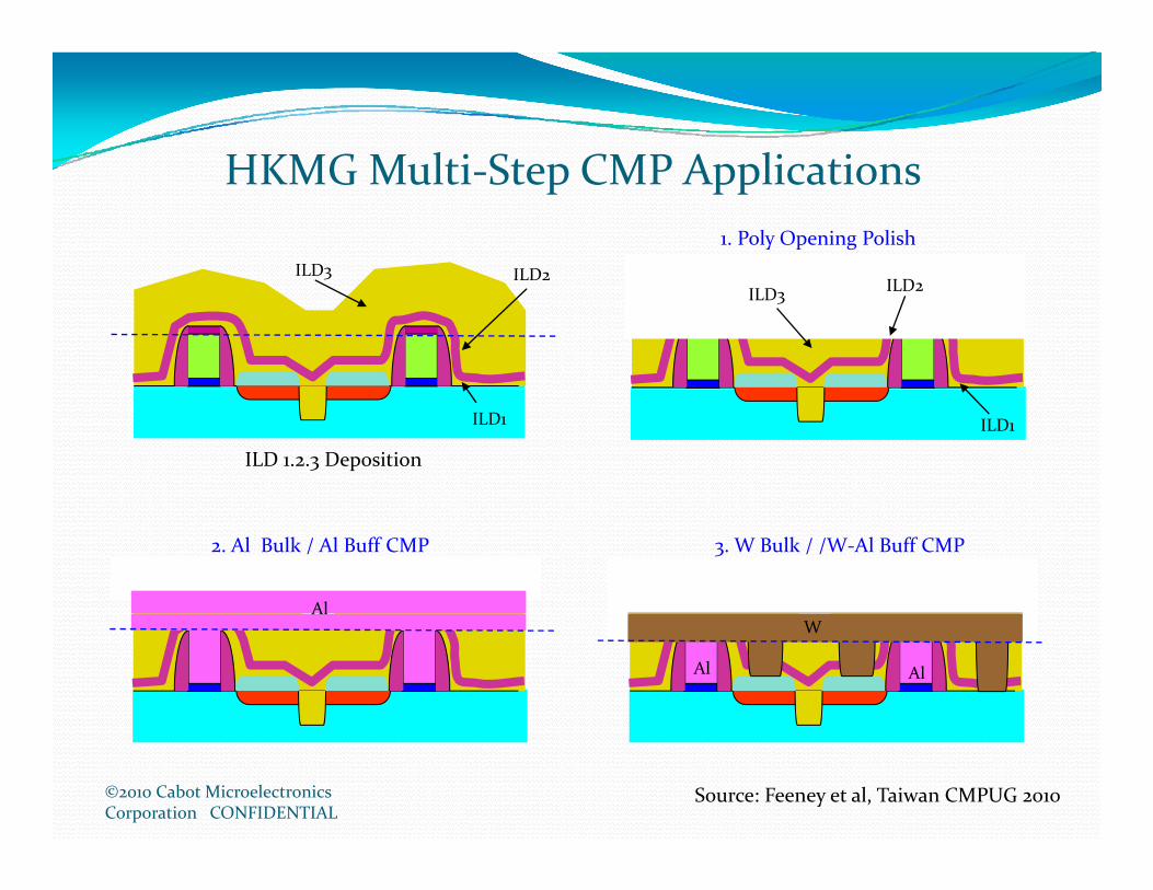
HKMG Multi Step CMP ApplicationsHKMG Multi‐Step CMP Applications1. Poly Opening Polish
ILD3 ILD2 ILD3 ILD2
3 ILD2
ILD1
ILD 1.2.3 Deposition
ILD1
2. Al Bulk / Al Buff CMP
Al
3. W Bulk / /W‐Al Buff CMP
Al
Al Al
W
©2010 Cabot Microelectronics Corporation CONFIDENTIAL
Source: Feeney et al, Taiwan CMPUG 2010

Approach to Meeting Today’s Tolerances: Copper CMP for Interconnects
Donald Canaperi
November 14, 2010
1) Copper CMP
2) “Barrier” CMPLiner/seed Hardmask 2
Hardmask 1
ULK Dielectric
Hardmask 1
Dielectric
Cap
Traditional CMP for interconnects is a two step process1) Copper CMP stopping on barrier2) Barrier CMP to non-selectively remove liner, hardmasks, and some dielectric) y , ,
Approach for upcoming nodes is to tailor the selectivity of each step-Copper CMP stopping on barrier-Selective removal, if necessary, of barrier stopping on hardmask
© 2010 IBM Corporation17
, y, pp g-CMP of hardmask with tailored selectivity to slow down/stop in ULK dielectric
Source: Canaperi et al, ICPT 2010

Logic CMP Steps Growing Long TermLogic CMP Steps Growing Long Term1 u 0.25 u 65 nm 16 nmCMP Steps Passes CMP Steps Passes CMP Steps Passes CMP Steps PassesNone 0 Indirect STI 1 Direct STI Bulk 1 Direct STI Bulk 1
Premetal Diel 1 Direct STI Final 1 Direct STI Final 1W Contact 1 Premetal Diel 1 Premetal Diel 1W Contact Buff 1 W Contact 1 Metal Gate 1
W Buff 1 Stress Film 2W Buff 1 Stress Film 2Epi/Other 2Contact Bulk 1Contact Final 1Contact Buff 1Contact Buff 1
None 0 W Via 4 Cu Bulk 8 Cu Bulk 7W Via Buff 4 Cu Final 8 Cu Final 7Interlevel Diel 4 Ta Barrier 8 Ta Barrier 7
BEOL Min 1 4BEOL Min 2 4BEOL Min 3 4Cu TSV Bulk 1Cu TSV Final 1TSV Barrier 1TSV Barrier 1
Total 0 Total 16 Total 29 Total 47
Extension, New Source: Feeney, ICPT2008

Corollary to Moore: Add 4 CMP Steps/Node
50
40
50
zed
20
30
teps
Util
iz BEOL NewBEOL ExistingFEOL New
10
20
CMP
St
FEOL Existing
01u / 0 0.25u / 4 65nm / 8 16nm / 12
T h l N d /G ti
Slurries: 0 2 6 11
Technology Node/Generation
Source: Feeney, ICPT2008
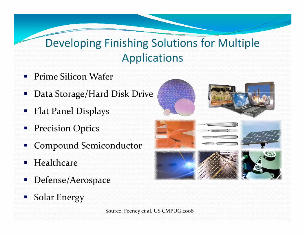
Developing Finishing Solutions for MultipleDeveloping Finishing Solutions for Multiple Applications
P i Sili W f Prime Silicon Wafer
Data Storage/Hard Disk Drive
Flat Panel Displays
Precision Opticsp
Compound Semiconductor
Healthcare Healthcare
Defense/Aerospace
Solar EnergySource: Feeney et al, US CMPUG 2008
Summary Continued innovation in Semiconductors is accelerating the changes Continued innovation in Semiconductors is accelerating the changes
in structures and materials, especially for transistors Several planarization applications require development today
C l i f li i i d i i l i Complexity of applications is driving more multi‐step processes Expect the planarization universe to continue expanding at a rate of
4 steps per technology generation4 p p gy g
Need to acknowledge the contribution of many people from Cabot Microelectronics IBM and the ITRS GroupsMicroelectronics, IBM, and the ITRS Groups
Are there other important applications not discussed here?