1. General description The PCA9511A is a hot swappable I 2 C-bus and SMBus buffer that allows I/O card insertion into a live backplane without corrupting the data and clock buses. Control circuitry prevents the backplane from being connected to the card until a stop command or bus idle occurs on the backplane without bus contention on the card. When the connection is made, the PCA9511A provides bidirectional buffering, keeping the backplane and card capacitances isolated. The PCA9511A rise time accelerator circuitry allows the use of weaker DC pull-up currents while still meeting rise time requirements. The PCA9511A incorporates a digital ENABLE input pin, which enables the device when asserted HIGH and forces the device into a low current mode when asserted LOW, and an open-drain READY output pin, which indicates that the backplane and card sides are connected together (HIGH) or not (LOW). During insertion, the PCA9511A SDA and SCL lines are precharged to 1 V to minimize the current required to charge the parasitic capacitance of the chip. 2. Features ■ Bidirectional buffer for SDA and SCL lines increases fan out and prevents SDA and SCL corruption during live board insertion and removal from multipoint backplane systems ■ Compatible with I 2 C-bus Standard-mode, I 2 C-bus Fast-mode, and SMBus standards ■ Built-in ∆V/∆t rise time accelerators on all SDA and SCL lines (0.6 V threshold) requires the bus pull-up voltage and supply voltage (V CC ) to be the same ■ Active HIGH ENABLE input ■ Active HIGH READY open-drain output ■ High-impedance SDA and SCL pins for V CC =0V ■ 1 V precharge on all SDA and SCL lines ■ Supporting clock stretching and multiple master arbitration/synchronization ■ Operating power supply voltage range: 2.7 V to 5.5 V ■ 0 Hz to 400 kHz clock frequency ■ ESD protection exceeds 2000 V HBM per JESD22-A114, 200 V MM per JESD22-A115, and 1000 V CDM per JESD22-C101 ■ Latch-up testing is done to JEDEC Standard JESD78 which exceeds 100 mA ■ Packages offered: SO8, TSSOP8 (MSOP8) PCA9511A Hot swappable I 2 C-bus and SMBus bus buffer Rev. 04 — 19 August 2009 Product data sheet
Transcript
1. General description
The PCA9511A is a hot swappable I2C-bus and SMBus buffer that allows I/O cardinsertion into a live backplane without corrupting the data and clock buses. Controlcircuitry prevents the backplane from being connected to the card until a stop command orbus idle occurs on the backplane without bus contention on the card. When theconnection is made, the PCA9511A provides bidirectional buffering, keeping thebackplane and card capacitances isolated.
The PCA9511A rise time accelerator circuitry allows the use of weaker DC pull-upcurrents while still meeting rise time requirements. The PCA9511A incorporates a digitalENABLE input pin, which enables the device when asserted HIGH and forces the deviceinto a low current mode when asserted LOW, and an open-drain READY output pin, whichindicates that the backplane and card sides are connected together (HIGH) or not (LOW).
During insertion, the PCA9511A SDA and SCL lines are precharged to 1 V to minimizethe current required to charge the parasitic capacitance of the chip.
2. Features
n Bidirectional buffer for SDA and SCL lines increases fan out and prevents SDA andSCL corruption during live board insertion and removal from multipoint backplanesystems
n Compatible with I2C-bus Standard-mode, I2C-bus Fast-mode, and SMBus standards
n Built-in ∆V/∆t rise time accelerators on all SDA and SCL lines (0.6 V threshold)requires the bus pull-up voltage and supply voltage (VCC) to be the same
n Active HIGH ENABLE input
n Active HIGH READY open-drain output
n High-impedance SDA and SCL pins for VCC = 0 V
n 1 V precharge on all SDA and SCL lines
n Supporting clock stretching and multiple master arbitration/synchronization
n Operating power supply voltage range: 2.7 V to 5.5 V
n 0 Hz to 400 kHz clock frequency
n ESD protection exceeds 2000 V HBM per JESD22-A114, 200 V MM perJESD22-A115, and 1000 V CDM per JESD22-C101
n Latch-up testing is done to JEDEC Standard JESD78 which exceeds 100 mA
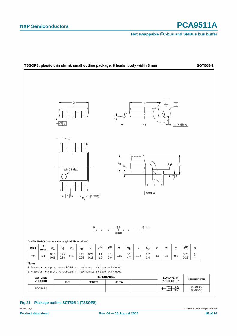
n Packages offered: SO8, TSSOP8 (MSOP8)
PCA9511AHot swappable I 2C-bus and SMBus bus bufferRev. 04 — 19 August 2009 Product data sheet
NXP Semiconductors PCA9511AHot swappable I 2C-bus and SMBus bus buffer
3. Applications
n cPCI, VME, AdvancedTCA cards and other multipoint backplane cards that arerequired to be inserted or removed from an operating system
Product data sheet Rev. 04 — 19 August 2009 3 of 24
NXP Semiconductors PCA9511AHot swappable I 2C-bus and SMBus bus buffer
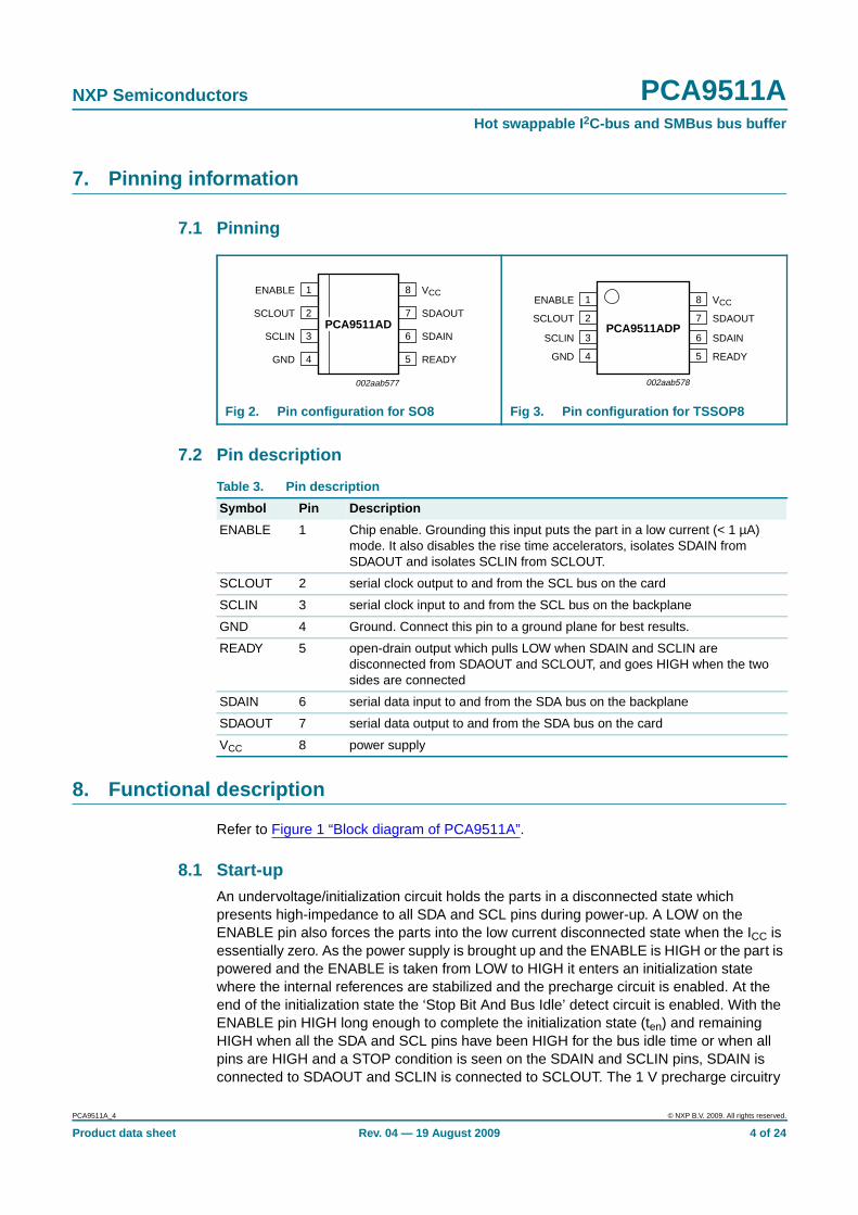
7. Pinning information
7.1 Pinning
7.2 Pin description
8. Functional description
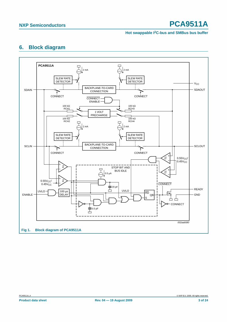
Refer to Figure 1 “Block diagram of PCA9511A”.
8.1 Start-upAn undervoltage/initialization circuit holds the parts in a disconnected state whichpresents high-impedance to all SDA and SCL pins during power-up. A LOW on theENABLE pin also forces the parts into the low current disconnected state when the ICC isessentially zero. As the power supply is brought up and the ENABLE is HIGH or the part ispowered and the ENABLE is taken from LOW to HIGH it enters an initialization statewhere the internal references are stabilized and the precharge circuit is enabled. At theend of the initialization state the ‘Stop Bit And Bus Idle’ detect circuit is enabled. With theENABLE pin HIGH long enough to complete the initialization state (ten) and remainingHIGH when all the SDA and SCL pins have been HIGH for the bus idle time or when allpins are HIGH and a STOP condition is seen on the SDAIN and SCLIN pins, SDAIN isconnected to SDAOUT and SCLIN is connected to SCLOUT. The 1 V precharge circuitry
Fig 2. Pin configuration for SO8 Fig 3. Pin configuration for TSSOP8
ENABLE VCC
SCLOUT SDAOUT
SCLIN SDAIN
GND READY
002aab577
1
2
3
4
6
5
8
7PCA9511AD PCA9511ADP
ENABLE VCC
SCLOUT SDAOUT
SCLIN SDAIN
GND READY
002aab578
1
2
3
4
6
5
8
7
Table 3. Pin description
Symbol Pin Description
ENABLE 1 Chip enable. Grounding this input puts the part in a low current (< 1 µA)mode. It also disables the rise time accelerators, isolates SDAIN fromSDAOUT and isolates SCLIN from SCLOUT.
SCLOUT 2 serial clock output to and from the SCL bus on the card
SCLIN 3 serial clock input to and from the SCL bus on the backplane
GND 4 Ground. Connect this pin to a ground plane for best results.
READY 5 open-drain output which pulls LOW when SDAIN and SCLIN aredisconnected from SDAOUT and SCLOUT, and goes HIGH when the twosides are connected
SDAIN 6 serial data input to and from the SDA bus on the backplane
SDAOUT 7 serial data output to and from the SDA bus on the card
Product data sheet Rev. 04 — 19 August 2009 4 of 24
NXP Semiconductors PCA9511AHot swappable I 2C-bus and SMBus bus buffer
is activated during the initialization and is deactivated when the connection is made. Theprecharge circuitry pulls up the SDA and SCL pins to 1 V through individual 100 kΩnominal resistors. This precharges the pins to 1 V to minimize the worst casedisturbances that result from inserting a card into the backplane where the backplane andthe card are at opposite logic levels.
8.2 Connect circuitryOnce the connection circuitry is activated, the behavior of SDAIN and SDAOUT as well asSCLIN and SCLOUT become identical with each acting as a bidirectional buffer thatisolates the input capacitance from the output bus capacitance while communicating thelogic levels. A LOW forced on either SDAIN or SDAOUT will cause the other pin to bedriven to a LOW by the part. The same is also true for the SCL pins. Noise between0.7VCC and VCC is generally ignored because a falling edge is only recognized when itfalls below 0.7VCC with a slew rate of at least 1.25 V/µs. When a falling edge is seen onone pin, the other pin in the pair turns on a pull-down driver that is referenced to a smallvoltage above the falling pin. The driver will pull the pin down at a slew rate determined bythe driver and the load initially, because it does not start until the first falling pin is below0.7VCC. The first falling pin may have a fast or slow slew rate, if it is faster than the pulldown slew rate then the initial pull-down rate will continue. If the first falling pin has a slowslew rate then the second pin will be pulled down at its initial slew rate only until it is justabove the first pin voltage then they will both continue down at the slew rate of the first.
Once both sides are LOW they will remain LOW until all the external drivers have stoppeddriving LOWs. If both sides are being driven LOW to the same value for instance, 10 mVby external drivers, which is the case for clock stretching and is typically the case foracknowledge, and one side external driver stops driving that pin will rise until the internaldriver pulls it down to the offset voltage. When the last external driver stops driving aLOW, that pin will rise up and settle out just above the other pin as both rise together witha slew rate determined by the internal slew rate control and the RC time constant. As longas the slew rate is at least 1.25 V/µs, when the pin voltage exceeds 0.6 V for thePCA9511A, the rise time accelerator’s circuits are turned on and the pull-down driver isturned off.
8.3 Maximum number of devices in seriesEach buffer adds about 0.1 V dynamic level offset at 25 °C with the offset larger at highertemperatures. Maximum offset (Voffset) is 0.150 V with a 10 kΩ pull-up resistor. The LOWlevel at the signal origination end (master) is dependent upon the load and the onlyspecification point is that the I2C-bus specification of 3 mA will produce VOL < 0.4 V,although if lightly loaded the VOL may be ~0.1 V. Assuming VOL = 0.1 V and Voffset = 0.1 V,the level after four buffers would be 0.5 V, which is only about 0.1 V below the threshold ofthe rising edge accelerator (about 0.6 V). With great care a system with four buffers maywork, but as the VOL moves up from 0.1 V, noise or bounces on the line will result in firingthe rising edge accelerator thus introducing false clock edges. Generally it isrecommended to limit the number of buffers in series to two, and to keep the load light tominimize the offset.
The PCA9510A (rise time accelerator is permanently disabled) and the PCA9512A (risetime accelerator can be turned off) are a little different with the rise time accelerator turnedoff because the rise time accelerator will not pull the node up, but the same logic that turns
Product data sheet Rev. 04 — 19 August 2009 5 of 24
NXP Semiconductors PCA9511AHot swappable I 2C-bus and SMBus bus buffer
on the accelerator turns the pull-down off. If the VIL is above ~0.6 V and a rising edge isdetected, the pull-down will turn off and will not turn back on until a falling edge isdetected.
Consider a system with three buffers connected to a common node and communicationbetween the Master and Slave B that are connected at either end of buffer A and buffer Bin series as shown in Figure 4. Consider if the VOL at the input of buffer A is 0.3 V and theVOL of Slave B (when acknowledging) is 0.4 V with the direction changing from Master toSlave B and then from Slave B to Master. Before the direction change you would observeVIL at the input of buffer A of 0.3 V and its output, the common node, is ~0.4 V. The outputof buffer B and buffer C would be ~0.5 V, but Slave B is driving 0.4 V, so the voltage atSlave B is 0.4 V. The output of buffer C is ~0.5 V. When the Master pull-down turns off, theinput of buffer A rises and so does its output, the common node, because it is the only partdriving the node. The common node will rise to 0.5 V before buffer B’s output turns on, ifthe pull-up is strong the node may bounce. If the bounce goes above the threshold for therising edge accelerator ~0.6 V the accelerators on both buffer A and buffer C will firecontending with the output of buffer B. The node on the input of buffer A will go HIGH aswill the input node of buffer C. After the common node voltage is stable for a while therising edge accelerators will turn off and the common node will return to ~0.5 V becausethe buffer B is still on. The voltage at both the Master and Slave C nodes would then fall to~0.6 V until Slave B turned off. This would not cause a failure on the data line as long asthe return to 0.5 V on the common node (~0.6 V at the Master and Slave C) occurredbefore the data setup time. If this were the SCL line, the parts on buffer A and buffer Cwould see a false clock rather than a stretched clock, which would cause a system error.
8.4 Propagation delaysThe delay for a rising edge is determined by the combined pull-up current from the busresistors and the rise time accelerator current source and the effective capacitance on thelines. If the pull-up currents are the same, any difference in rise time is directlyproportional to the difference in capacitance between the two sides. The tPLH may benegative if the output capacitance is less than the input capacitance and would be positiveif the output capacitance is larger than the input capacitance, when the currents are thesame.
The tPHL can never be negative because the output does not start to fall until the input isbelow 0.7VCC, and the output turn on has a non-zero delay, and the output has a limitedmaximum slew rate, and even if the input slew rate is slow enough that the output catchesup it will still lag the falling voltage of the input by the offset voltage. The maximum tPHLoccurs when the input is driven LOW with zero delay and the output is still limited by its
Fig 4. System with 3 buffers connected to common node
Product data sheet Rev. 04 — 19 August 2009 6 of 24
NXP Semiconductors PCA9511AHot swappable I 2C-bus and SMBus bus buffer
turn-on delay and the falling edge slew rate. The output falling edge slew rate is a functionof the internal maximum slew rate which is a function of temperature, VCC and process, aswell as the load current and the load capacitance.
8.5 Rise time acceleratorsDuring positive bus transitions a 2 mA current source is switched on to quickly slew theSDA and SCL lines HIGH once the input level of 0.6 V for the PCA9511A is exceeded.The rising edge rate should be at least 1.25 V/µs to guarantee turn on of the accelerators.The built-in ∆V/∆t rise time accelerators on all SDA and SCL lines requires the bus pull-upvoltage and supply voltage (VCC) to be the same.
8.6 READY digital outputThis pin provides a digital flag which is LOW when either ENABLE is LOW or the start-upsequence described earlier in this section has not been completed. READY goes HIGHwhen ENABLE is HIGH and start-up is complete. The pin is driven by an open-drainpull-down capable of sinking 3 mA while holding 0.4 V on the pin. Connect a resistor of10 kΩ to VCC to provide the pull-up.
8.7 ENABLE low current disableGrounding the ENABLE pin disconnects the backplane side from the card side, disablesthe rise time accelerators, drives READY LOW, disables the bus precharge circuitry, andputs the part in a low current state. When the pin voltage is driven all the way to VCC, thepart waits for data transactions on both the backplane and card sides to be completebefore reconnecting the two sides.
8.8 Resistor pull-up value selectionThe system pull-up resistors must be strong enough to provide a positive slew rate of1.25 V/µs on the SDA and SCL pins, in order to activate the boost pull-up currents duringrising edges. Choose maximum resistor value using the formula given in Equation 1:
(1)
where R is the pull-up resistor value in Ω, VCC(min) is the minimum VCC voltage in volts,and C is the equivalent bus capacitance in picofarads (pF).
In addition, regardless of the bus capacitance, always choose R ≤ 65.7 kΩ for VCC = 5.5 Vmaximum, R ≤ 45 kΩ for VCC = 3.6 V maximum. The start-up circuitry requires logic HIGHvoltages on SDAOUT and SCLOUT to connect the backplane to the card, and thesepull-up values are needed to overcome the precharge voltage. See the curves in Figure 5and Figure 6 for guidance in resistor pull-up selection.
Product data sheet Rev. 04 — 19 August 2009 8 of 24
NXP Semiconductors PCA9511AHot swappable I 2C-bus and SMBus bus buffer
8.9 Hot swapping and capacitance buffering applicationFigure 7 through Figure 10 illustrate the usage of the PCA9511A in applications that takeadvantage of both its hot swapping and capacitance buffering features. In all of theseapplications, note that if the I/O cards were plugged directly into the backplane, all of thebackplane and card capacitances would add directly together, making rise time andfall time requirements difficult to meet. Placing a bus buffer on the edge of each card,however, isolates the card capacitance from the backplane. For a given I/O card, thePCA9511A drives the capacitance of everything on the card and the backplane must driveonly the capacitance of the bus buffer, which is less than 10 pF, the connector, trace, andall additional cards on the backplane.
See Application Note AN10160, ‘Hot Swap Bus Buffer’ for more information onapplications and technical assistance.
Remark: The PCA9511A can be used in any combination depending on the number of rise time accelerators that are neededby the system. Normally only one PCA9511A would be required per bus.
Fig 7. Hot swapping multiple I/O cards into a backplane using the PCA9511A in a cPCI, VME, and AdvancedTCAsystem
Product data sheet Rev. 04 — 19 August 2009 9 of 24
NXP Semiconductors PCA9511AHot swappable I 2C-bus and SMBus bus buffer
Fig 8. Hot swapping multiple I/O cards into a backplane using the PCA9511A in a PCI system
002aab585
R410 kΩ
C10.01 µF
SDAOUTSCLOUT
READY
VCC
GND
R510 kΩ
R610 kΩ
ENABLESDAINSCLIN
CARD1_SDACARD1_SCL
STA
GG
ER
ED
CO
NN
EC
TOR
I/O PERIPHERAL CARD 1
BACKPLANECONNECTOR
R810 kΩ
C30.01 µF
SDAOUTSCLOUT
READY
VCC
GND
R910 kΩ
R1010 kΩ
ENABLESDAINSCLIN
CARD2_SDACARD2_SCL
STA
GG
ER
ED
CO
NN
EC
TOR
I/O PERIPHERAL CARD 2
R210 kΩ
R110 kΩ
VCC
BACKPLANE
SDASCL
C40.01 µF
C20.01 µF
Remark: See Application Note AN255, ‘I2C repeaters, hubs, and expanders’ for more information on other devices betteroptimized for long distance transmission of the I2C-bus or SMBus.
Fig 9. Repeater/bus extender application using the PCA9511A
Product data sheet Rev. 04 — 19 August 2009 12 of 24
NXP Semiconductors PCA9511AHot swappable I 2C-bus and SMBus bus buffer
[1] This specification applies over the full operating temperature range.
[2] The enable time can slow considerably for some parts when temperature is < −20 °C.
[3] Delays that can occur after ENABLE and/or idle times have passed.
[4] Guaranteed by design, not production tested.
[5] Itrt(pu) varies with temperature and VCC voltage, as shown in Section 11.1 “Typical performance characteristics”.
[6] Input pull-up voltage should not exceed power supply voltage in operating mode because the rise time accelerator will clamp the voltageto the positive supply rail.
[7] The connection circuitry always regulates its output to a higher voltage than its input. The magnitude of this offset voltage as a functionof the pull-up resistor and VCC voltage is shown in Section 11.1 “Typical performance characteristics”.
[8] Cb = total capacitance of one bus line in pF.
Input-output connection
Voffset offset voltage 10 kΩ to VCC on SDA, SCL;VCC = 3.3 V
[1][7][9] 0 110 175 mV
tPLH LOW to HIGHpropagation delay
SCL to SCL and SDA to SDA;10 kΩ to VCC;CL = 100 pF each side
- 0 - ns
tPHL HIGH to LOWpropagation delay
SCL to SCL and SDA to SDA;10 kΩ to VCC;CL = 100 pF each side
- 70 - ns
Ci(SCL/SDA) SCL and SDA inputcapacitance
[4] - 5 7 pF
VOL LOW-level outputvoltage
VI = 0 V; SDAn, SCLn pins;Isink = 3 mA; VCC = 2.7 V
[1] 0 - 0.4 V
ILI input leakage current SDAn, SCLn pins; VCC = 5.5 V −1 - +1 µA
System characteristics
fSCL SCL clock frequency [4] 0 - 400 kHz
tBUF bus free time between aSTOP and STARTcondition
[4] 1.3 - - µs
tHD;STA hold time (repeated)START condition
[4] 0.6 - - µs
tSU;STA set-up time for arepeatedSTART condition
[4] 0.6 - - µs
tSU;STO set-up time forSTOP condition
[4] 0.6 - - µs
tHD;DAT data hold time [4] 300 - - ns
tSU;DAT data set-up time [4] 100 - - ns
tLOW LOW period of theSCL clock
[4] 1.3 - - µs
tHIGH HIGH period of theSCL clock
[4] 0.6 - - µs
tf fall time of both SDA andSCL signals
[4][8] 20 + 0.1 × Cb - 300 ns
tr rise time of both SDAand SCL signals
[4][8] 20 + 0.1 × Cb - 300 ns
Table 5. Characteristics …continuedVCC = 2.7 V to 5.5 V; Tamb = −40 °C to +85 V; unless otherwise specified.
Product data sheet Rev. 04 — 19 August 2009 18 of 24
NXP Semiconductors PCA9511AHot swappable I 2C-bus and SMBus bus buffer
14. Soldering of SMD packages
This text provides a very brief insight into a complex technology. A more in-depth accountof soldering ICs can be found in Application Note AN10365 “Surface mount reflowsoldering description”.
14.1 Introduction to solderingSoldering is one of the most common methods through which packages are attached toPrinted Circuit Boards (PCBs), to form electrical circuits. The soldered joint provides boththe mechanical and the electrical connection. There is no single soldering method that isideal for all IC packages. Wave soldering is often preferred when through-hole andSurface Mount Devices (SMDs) are mixed on one printed wiring board; however, it is notsuitable for fine pitch SMDs. Reflow soldering is ideal for the small pitches and highdensities that come with increased miniaturization.
14.2 Wave and reflow solderingWave soldering is a joining technology in which the joints are made by solder coming froma standing wave of liquid solder. The wave soldering process is suitable for the following:
• Through-hole components
• Leaded or leadless SMDs, which are glued to the surface of the printed circuit board
Not all SMDs can be wave soldered. Packages with solder balls, and some leadlesspackages which have solder lands underneath the body, cannot be wave soldered. Also,leaded SMDs with leads having a pitch smaller than ~0.6 mm cannot be wave soldered,due to an increased probability of bridging.
The reflow soldering process involves applying solder paste to a board, followed bycomponent placement and exposure to a temperature profile. Leaded packages,packages with solder balls, and leadless packages are all reflow solderable.
Key characteristics in both wave and reflow soldering are:
• Board specifications, including the board finish, solder masks and vias
• Package footprints, including solder thieves and orientation
• The moisture sensitivity level of the packages
• Package placement
• Inspection and repair
• Lead-free soldering versus SnPb soldering
14.3 Wave solderingKey characteristics in wave soldering are:
• Process issues, such as application of adhesive and flux, clinching of leads, boardtransport, the solder wave parameters, and the time during which components areexposed to the wave
• Solder bath specifications, including temperature and impurities
Product data sheet Rev. 04 — 19 August 2009 19 of 24
NXP Semiconductors PCA9511AHot swappable I 2C-bus and SMBus bus buffer
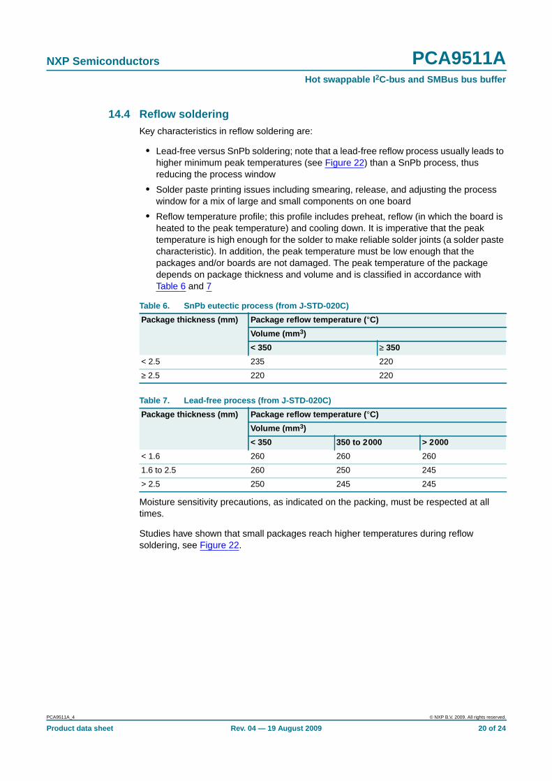
14.4 Reflow solderingKey characteristics in reflow soldering are:
• Lead-free versus SnPb soldering; note that a lead-free reflow process usually leads tohigher minimum peak temperatures (see Figure 22) than a SnPb process, thusreducing the process window
• Solder paste printing issues including smearing, release, and adjusting the processwindow for a mix of large and small components on one board
• Reflow temperature profile; this profile includes preheat, reflow (in which the board isheated to the peak temperature) and cooling down. It is imperative that the peaktemperature is high enough for the solder to make reliable solder joints (a solder pastecharacteristic). In addition, the peak temperature must be low enough that thepackages and/or boards are not damaged. The peak temperature of the packagedepends on package thickness and volume and is classified in accordance withTable 6 and 7
Moisture sensitivity precautions, as indicated on the packing, must be respected at alltimes.
Studies have shown that small packages reach higher temperatures during reflowsoldering, see Figure 22.
Table 6. SnPb eutectic process (from J-STD-020C)
Package thickness (mm) Package reflow temperature ( °C)
Volume (mm 3)
< 350 ≥ 350
< 2.5 235 220
≥ 2.5 220 220
Table 7. Lead-free process (from J-STD-020C)
Package thickness (mm) Package reflow temperature ( °C)
Product data sheet Rev. 04 — 19 August 2009 21 of 24
NXP Semiconductors PCA9511AHot swappable I 2C-bus and SMBus bus buffer
16. Revision history
Table 9. Revision history
Document ID Release date Data sheet status Change notice Supersedes
PCA9511A_4 20090819 Product data sheet - PCA9511A_3
Modifications: • Section 8.8 “Resistor pull-up value selection”, 2nd paragraph, 1st sentence: changed from“... always choose R ≤ 16 kΩ for VCC = 5.5 V maximum, R ≤ 24 kΩ for VCC = 3.6 V maximum.”to “... always choose R ≤ 65.7 kΩ for VCC = 5.5 V maximum, R ≤ 45 kΩ for VCC = 3.6 Vmaximum.”
• Figure 5 “Bus requirements for 3.3 V systems” updated:
– changed from “rise time > 300 ns” to “rise time = 300 ns”
– changed from “rise time < 20 ns” to “rise time = 20 ns”
• Figure 6 “Bus requirements for 5 V systems” updated:
– changed from “rise time > 300 ns” to “rise time = 300 ns”
– changed from “rise time < 20 ns” to “rise time = 20 ns”
PCA9511A_3 20090720 Product data sheet - PCA9511A_2
PCA9511A_2 20090528 Product data sheet - PCA9511A_1
Product data sheet Rev. 04 — 19 August 2009 22 of 24
NXP Semiconductors PCA9511AHot swappable I 2C-bus and SMBus bus buffer
17. Legal information
17.1 Data sheet status
[1] Please consult the most recently issued document before initiating or completing a design.
[2] The term ‘short data sheet’ is explained in section “Definitions”.
[3] The product status of device(s) described in this document may have changed since this document was published and may differ in case of multiple devices. The latest product statusinformation is available on the Internet at URL http://www.nxp.com.
17.2 Definitions
Draft — The document is a draft version only. The content is still underinternal review and subject to formal approval, which may result inmodifications or additions. NXP Semiconductors does not give anyrepresentations or warranties as to the accuracy or completeness ofinformation included herein and shall have no liability for the consequences ofuse of such information.
Short data sheet — A short data sheet is an extract from a full data sheetwith the same product type number(s) and title. A short data sheet is intendedfor quick reference only and should not be relied upon to contain detailed andfull information. For detailed and full information see the relevant full datasheet, which is available on request via the local NXP Semiconductors salesoffice. In case of any inconsistency or conflict with the short data sheet, thefull data sheet shall prevail.
17.3 Disclaimers
General — Information in this document is believed to be accurate andreliable. However, NXP Semiconductors does not give any representations orwarranties, expressed or implied, as to the accuracy or completeness of suchinformation and shall have no liability for the consequences of use of suchinformation.
Right to make changes — NXP Semiconductors reserves the right to makechanges to information published in this document, including withoutlimitation specifications and product descriptions, at any time and withoutnotice. This document supersedes and replaces all information supplied priorto the publication hereof.
Suitability for use — NXP Semiconductors products are not designed,authorized or warranted to be suitable for use in medical, military, aircraft,space or life support equipment, nor in applications where failure ormalfunction of an NXP Semiconductors product can reasonably be expectedto result in personal injury, death or severe property or environmental
damage. NXP Semiconductors accepts no liability for inclusion and/or use ofNXP Semiconductors products in such equipment or applications andtherefore such inclusion and/or use is at the customer’s own risk.
Applications — Applications that are described herein for any of theseproducts are for illustrative purposes only. NXP Semiconductors makes norepresentation or warranty that such applications will be suitable for thespecified use without further testing or modification.
Limiting values — Stress above one or more limiting values (as defined inthe Absolute Maximum Ratings System of IEC 60134) may cause permanentdamage to the device. Limiting values are stress ratings only and operation ofthe device at these or any other conditions above those given in theCharacteristics sections of this document is not implied. Exposure to limitingvalues for extended periods may affect device reliability.
Terms and conditions of sale — NXP Semiconductors products are soldsubject to the general terms and conditions of commercial sale, as publishedat http://www.nxp.com/profile/terms, including those pertaining to warranty,intellectual property rights infringement and limitation of liability, unlessexplicitly otherwise agreed to in writing by NXP Semiconductors. In case ofany inconsistency or conflict between information in this document and suchterms and conditions, the latter will prevail.
No offer to sell or license — Nothing in this document may be interpretedor construed as an offer to sell products that is open for acceptance or thegrant, conveyance or implication of any license under any copyrights, patentsor other industrial or intellectual property rights.
Export control — This document as well as the item(s) described hereinmay be subject to export control regulations. Export might require a priorauthorization from national authorities.
17.4 TrademarksNotice: All referenced brands, product names, service names and trademarksare the property of their respective owners.
I2C-bus — logo is a trademark of NXP B.V.
18. Contact information
For more information, please visit: http://www .nxp.com
For sales office addresses, please send an email to: salesad [email protected]
Document status [1] [2] Product status [3] Definition
Objective [short] data sheet Development This document contains data from the objective specification for product development.
Preliminary [short] data sheet Qualification This document contains data from the preliminary specification.
Product [short] data sheet Production This document contains the product specification.