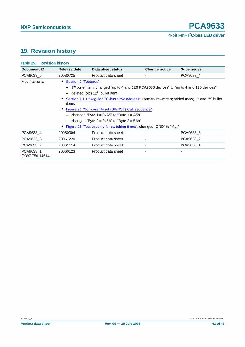
1. General description The PCA9633 is an I 2 C-bus controlled 4-bit LED driver optimized for Red/Green/Blue/Amber (RGBA) color mixing applications. Each LED output has its own 8-bit resolution (256 steps) fixed frequency Individual PWM controller that operates at 97 kHz with a duty cycle that is adjustable from 0 % to 99.6 % to allow the LED to be set to a specific brightness value. A fifth 8-bit resolution (256 steps) Group PWM controller has both a fixed frequency of 190 Hz and an adjustable frequency between 24 Hz to once every 10.73 seconds with a duty cycle that is adjustable from 0 % to 99.6 % that is used to either dim or blink all LEDs with the same value. Each LED output can be off, on (no PWM control), set at its Individual PWM controller value or at both Individual and Group PWM controller values. The LED output driver is programmed to be either open-drain with a 25 mA current sink capability at 5 V or totem pole with a 25 mA sink, 10 mA source capability at 5 V. The PCA9633 operates with a supply voltage range of 2.3 V to 5.5 V and the outputs are 5.5 V tolerant. LEDs can be directly connected to the LED output (up to 25 mA, 5.5 V) or controlled with external drivers and a minimum amount of discrete components for larger current or higher voltage LEDs. The PCA9633 is one of the first LED controller devices in a new Fast-mode Plus (Fm+) family. Fm+ devices offer higher frequency (up to 1 MHz) and more densely populated bus operation (up to 4000 pF). The active LOW Output Enable input pin ( OE) allows asynchronous control of the LED outputs and can be used to set all the outputs to a defined I 2 C-bus programmable logic state. The OE can also be used to externally PWM the outputs, which is useful when multiple devices need to be dimmed or blinked together using software control. This feature is available for the 16-pin version only. Software programmable LED Group and three Sub Call I 2 C addresses allow all or defined groups of PCA9633 devices to respond to a common I 2 C address, allowing for example, all red LEDs to be turned on or off at the same time or marquee chasing effect, thus minimizing I 2 C-bus commands. The PCA9633 is offered with 3 different I 2 C-bus address options: fixed I 2 C-bus address (8-pin version), 4 different I 2 C-bus addresses from 2 programmable address pins (10-pin version), and 126 different I 2 C-bus addresses from 7 programmable address pins (16-pin version). They are software identical except for the different number of address combinations. The Software Reset (SWRST) Call allows the master to perform a reset of the PCA9633 through the I 2 C-bus, identical to the Power-On Reset (POR) that initializes the registers to their default state causing the outputs to be set HIGH (LED off). This allows an easy and quick way to reconfigure all device registers to the same condition. PCA9633 4-bit Fm+ I 2 C-bus LED driver Rev. 05 — 25 July 2008 Product data sheet
Transcript
1. General description
The PCA9633 is an I2C-bus controlled 4-bit LED driver optimized forRed/Green/Blue/Amber (RGBA) color mixing applications. Each LED output has its own8-bit resolution (256 steps) fixed frequency Individual PWM controller that operates at97 kHz with a duty cycle that is adjustable from 0 % to 99.6 % to allow the LED to be setto a specific brightness value. A fifth 8-bit resolution (256 steps) Group PWM controllerhas both a fixed frequency of 190 Hz and an adjustable frequency between 24 Hz to onceevery 10.73 seconds with a duty cycle that is adjustable from 0 % to 99.6 % that is used toeither dim or blink all LEDs with the same value.
Each LED output can be off, on (no PWM control), set at its Individual PWM controllervalue or at both Individual and Group PWM controller values. The LED output driver isprogrammed to be either open-drain with a 25 mA current sink capability at 5 V or totempole with a 25 mA sink, 10 mA source capability at 5 V. The PCA9633 operates with asupply voltage range of 2.3 V to 5.5 V and the outputs are 5.5 V tolerant. LEDs can bedirectly connected to the LED output (up to 25 mA, 5.5 V) or controlled with externaldrivers and a minimum amount of discrete components for larger current or higher voltageLEDs.
The PCA9633 is one of the first LED controller devices in a new Fast-mode Plus (Fm+)family. Fm+ devices offer higher frequency (up to 1 MHz) and more densely populated busoperation (up to 4000 pF).
The active LOW Output Enable input pin (OE) allows asynchronous control of the LEDoutputs and can be used to set all the outputs to a defined I2C-bus programmable logicstate. The OE can also be used to externally PWM the outputs, which is useful whenmultiple devices need to be dimmed or blinked together using software control. Thisfeature is available for the 16-pin version only.
Software programmable LED Group and three Sub Call I2C addresses allow all or definedgroups of PCA9633 devices to respond to a common I2C address, allowing for example,all red LEDs to be turned on or off at the same time or marquee chasing effect, thusminimizing I2C-bus commands.
The PCA9633 is offered with 3 different I2C-bus address options: fixed I2C-bus address(8-pin version), 4 different I2C-bus addresses from 2 programmable address pins (10-pinversion), and 126 different I2C-bus addresses from 7 programmable address pins (16-pinversion). They are software identical except for the different number of addresscombinations.
The Software Reset (SWRST) Call allows the master to perform a reset of the PCA9633through the I2C-bus, identical to the Power-On Reset (POR) that initializes the registers totheir default state causing the outputs to be set HIGH (LED off). This allows an easy andquick way to reconfigure all device registers to the same condition.
PCA96334-bit Fm+ I 2C-bus LED driverRev. 05 — 25 July 2008 Product data sheet
NXP Semiconductors PCA96334-bit Fm+ I 2C-bus LED driver
2. Features
n 4 LED drivers. Each output programmable at:
u Off
u On
u Programmable LED brightness
u Programmable group dimming/blinking mixed with individual LED brightness
n 1 MHz Fast-mode Plus I2C-bus interface with 30 mA high drive capability on SDAoutput for driving high capacitive buses
n 256-step (8-bit) linear programmable brightness per LED output varying from fully off(default) to maximum brightness using a 97 kHz PWM signal
n 256-step group brightness control allows general dimming (using a 190 Hz PWMsignal) from fully off to maximum brightness (default)
n 256-step group blinking with frequency programmable from 24 Hz to 10.73 s andduty cycle from 0 % to 99.6 %
n Four totem pole outputs (sink 25 mA and source 10 mA at 5 V) with softwareprogrammable open-drain LED outputs selection (default at totem pole). No inputfunction.
n Output state change programmable on the Acknowledge or the STOP Command toupdate outputs byte-by-byte or all at the same time (default to ‘Change on STOP’).
n Active LOW Output Enable (OE) input pin. LED outputs programmable to ‘1’, ‘0’ or‘high-impedance’ (default at power-up) when OE is HIGH, thus allowing hardwareblinking and dimming of the LEDs (16-pin version only).
n 2 hardware address pins (10-pin version) and 7 hardware address pins (16-pinversion) allow respectively up to 4 and 126 devices to be connected to the sameI2C-bus. No hardware address pins in the 8-pin version.
n 4 software programmable I2C-bus addresses (one LED Group Call address and threeLED Sub Call addresses) allow groups of devices to be addressed at the same time inany combination (for example, one register used for ‘All Call’ so that all the PCA9633son the I2C-bus can be addressed at the same time and the second register used forthree different addresses so that 1⁄3 of all devices on the bus can be addressed at thesame time in a group). Software enable and disable for I2C-bus address.
n Software Reset feature (SWRST Call) allows the device to be reset through theI2C-bus
n 25 MHz internal oscillator requires no external components
n Internal power-on reset
n Noise filter on SDA/SCL inputs
n Edge rate control on outputs
n No glitch on power-up
n Supports hot insertion
n Low standby current
n Operating power supply voltage range of 2.3 V to 5.5 V
n 5.5 V tolerant inputs
n −40 °C to +85 °C operation
n ESD protection exceeds 2000 V HBM per JESD22-A114, 200 V MM perJESD22-A115, and 1000 V CDM per JESD22-C101
n Latch-up testing is done to JEDEC Standard JESD78 which exceeds 100 mA
NXP Semiconductors PCA96334-bit Fm+ I 2C-bus LED driver
[1] HVQFN16 package die supply ground is connected to both the VSS pin and the exposed center pad. TheVSS pin must be connected to supply ground for proper device operation. For enhanced thermal, electrical,and board-level performance, the exposed pad needs to be soldered to the board using a correspondingthermal pad on the board, and for proper heat conduction through the board thermal vias need to beincorporated in the PCB in the thermal pad region.
NXP Semiconductors PCA96334-bit Fm+ I 2C-bus LED driver
7. Functional description
Refer to Figure 1 “Block diagram of PCA9633”.
7.1 Device addressesFollowing a START condition, the bus master must output the address of the slave it isaccessing.
There are a maximum of 128 possible programmable addresses using the 7 hardwareaddress pins. Two of these addresses, Software Reset and LED All Call, cannot be usedbecause their default power-up state is ON, leaving a maximum of 126 addresses. Usingother reserved addresses, as well as any other subcall address, will reduce the totalnumber of possible addresses even further.
7.1.1 Regular I 2C-bus slave address
The I2C-bus slave address of the PCA9633 is shown in Figure 8. To conserve power, nointernal pull-up resistors are incorporated on the hardware selectable address pins andthey must be pulled HIGH or LOW (10-pin and 16-pin versions).
Remark: Using reserved I2C-bus addresses will interfere with other devices, but only if thedevices are on the bus and/or the bus will be open to other I2C-bus systems at some laterdate. In a closed system where the designer controls the address assignment theseaddresses can be used since the PCA9633 treats them like any other address. TheLED All Call, Software Reset and PCA9564 or PCA9665 slave address (if on the bus) cannever be used for individual device addresses.
• PCA9633 LED All Call address (1110 000) and Software Reset (0000 0110) whichare active on start-up
• PCA9564 (0000 000) or PCA9665 (1110 000) slave address which is active onstart-up
The last bit of the address byte defines the operation to be performed. When set to logic 1a read is selected, while a logic 0 selects a write operation.
a. 8-pin version b. 10-pin version c. 16-pin version
NXP Semiconductors PCA96334-bit Fm+ I 2C-bus LED driver
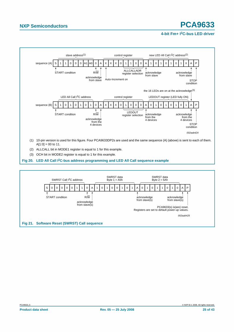
7.1.2 LED All Call I 2C-bus address
• Default power-up value (ALLCALLADR register): E0h or 1110 000X
• Programmable through I2C-bus (volatile programming)
• At power-up, LED All Call I2C-bus address is enabled. PCA9633 sends an ACK whenE0h (R/W = 0) or E1h (R/W = 1) is sent by the master.
See Section 7.3.8 “LED All Call I2C-bus address, ALLCALLADR” for more detail.
Remark: The default LED All Call I2C-bus address (E0h or 1110 000X) must not be usedas a regular I2C-bus slave address since this address is enabled at power-up. All thePCA9633s on the I2C-bus will acknowledge the address if sent by the I2C-bus master.
7.1.3 LED Sub Call I 2C-bus addresses
• 3 different I2C-bus addresses can be used
• Default power-up values:
– SUBADR1 register: E2h or 1110 001X
– SUBADR2 register: E4h or 1110 010X
– SUBADR3 register: E8h or 1110 100X
• Programmable through I2C-bus (volatile programming)
• At power-up, Sub Call I2C-bus addresses are disabled. PCA9633 does not send anACK when E2h (R/W = 0) or E3h (R/W = 1), E4h (R/W = 0) or E5h (R/W = 1), orE8h (R/W = 0) or E9h (R/W = 1) is sent by the master.
See Section 7.3.7 “I2C-bus subaddress 1 to 3, SUBADRx” for more detail.
Remark: The default LED Sub Call I2C-bus addresses may be used as regular I2C-busslave addresses as long as they are disabled.
7.1.4 Software Reset I 2C-bus address
The address shown in Figure 9 is used when a reset of the PCA9633 needs to beperformed by the master. The Software Reset address (SWRST Call) must be used withR/W = 0. If R/W = 1, the PCA9633 does not acknowledge the SWRST. See Section 7.6“Software Reset” for more detail.
Remark: The Software Reset I2C-bus address is a reserved address and cannot be usedas a regular I2C-bus slave address (16-pin version) or as an LED All Call or LED Sub Calladdress.
NXP Semiconductors PCA96334-bit Fm+ I 2C-bus LED driver
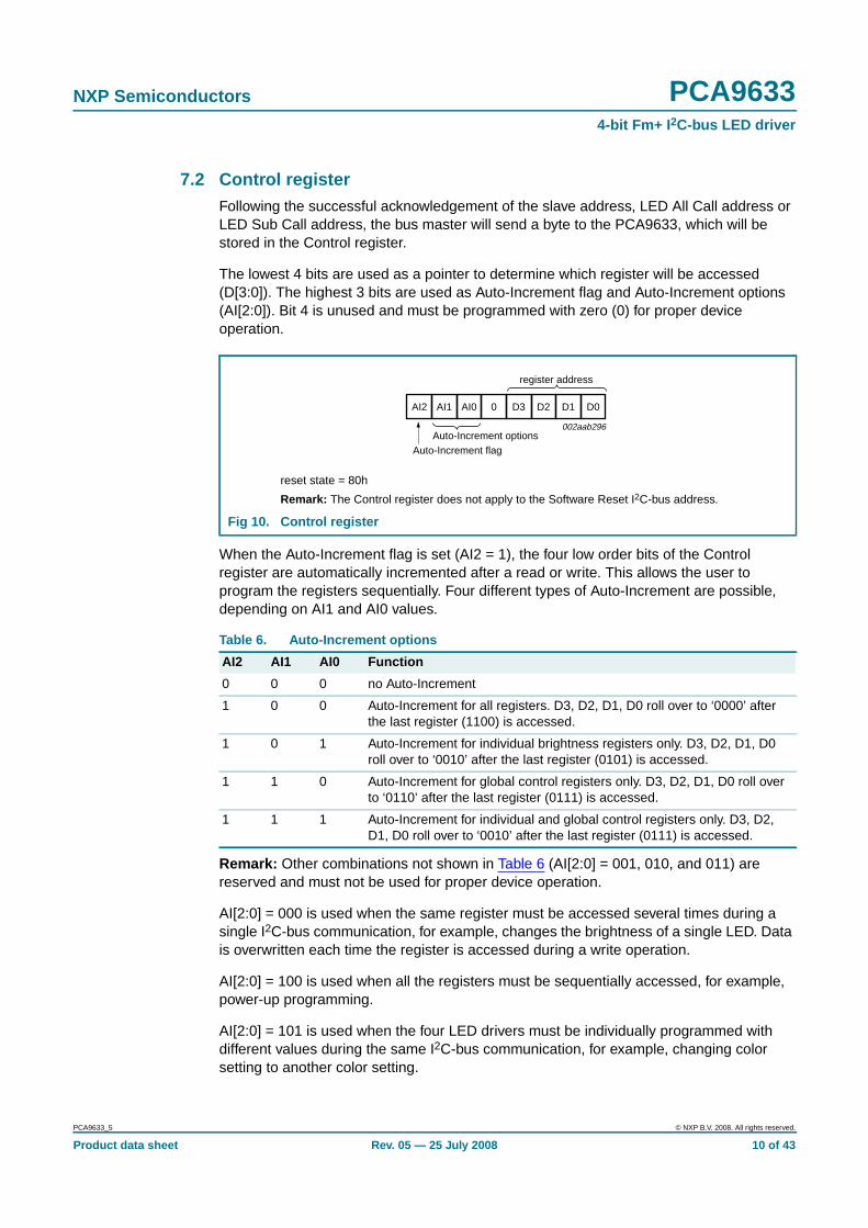
7.2 Control registerFollowing the successful acknowledgement of the slave address, LED All Call address orLED Sub Call address, the bus master will send a byte to the PCA9633, which will bestored in the Control register.
The lowest 4 bits are used as a pointer to determine which register will be accessed(D[3:0]). The highest 3 bits are used as Auto-Increment flag and Auto-Increment options(AI[2:0]). Bit 4 is unused and must be programmed with zero (0) for proper deviceoperation.
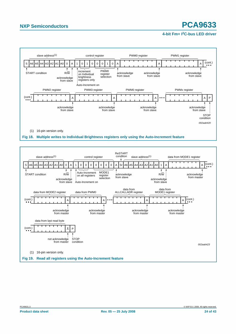
When the Auto-Increment flag is set (AI2 = 1), the four low order bits of the Controlregister are automatically incremented after a read or write. This allows the user toprogram the registers sequentially. Four different types of Auto-Increment are possible,depending on AI1 and AI0 values.
Remark: Other combinations not shown in Table 6 (AI[2:0] = 001, 010, and 011) arereserved and must not be used for proper device operation.
AI[2:0] = 000 is used when the same register must be accessed several times during asingle I2C-bus communication, for example, changes the brightness of a single LED. Datais overwritten each time the register is accessed during a write operation.
AI[2:0] = 100 is used when all the registers must be sequentially accessed, for example,power-up programming.
AI[2:0] = 101 is used when the four LED drivers must be individually programmed withdifferent values during the same I2C-bus communication, for example, changing colorsetting to another color setting.
reset state = 80h
Remark: The Control register does not apply to the Software Reset I2C-bus address.
Fig 10. Control register
Table 6. Auto-Increment options
AI2 AI1 AI0 Function
0 0 0 no Auto-Increment
1 0 0 Auto-Increment for all registers. D3, D2, D1, D0 roll over to ‘0000’ afterthe last register (1100) is accessed.
1 0 1 Auto-Increment for individual brightness registers only. D3, D2, D1, D0roll over to ‘0010’ after the last register (0101) is accessed.
1 1 0 Auto-Increment for global control registers only. D3, D2, D1, D0 roll overto ‘0110’ after the last register (0111) is accessed.
1 1 1 Auto-Increment for individual and global control registers only. D3, D2,D1, D0 roll over to ‘0010’ after the last register (0111) is accessed.
Product data sheet Rev. 05 — 25 July 2008 10 of 43
NXP Semiconductors PCA96334-bit Fm+ I 2C-bus LED driver
AI[2:0] = 110 is used when the LED drivers must be globally programmed with differentsettings during the same I2C-bus communication, for example, global brightness orblinking change.
AI[2:0] = 111 is used when individual and global changes must be performed during thesame I2C-bus communication, for example, changing a color and global brightness at thesame time.
Only the 4 least significant bits D[3:0] are affected by the AI[2:0] bits.
When the Control register is written, the register entry point determined by D[3:0] is thefirst register that will be addressed (read or write operation), and can be anywherebetween 0000 and 1100 (as defined in Table 7). When AI[2] = 1, the Auto-Increment flagis set and the rollover value at which the point where the register increment stops andgoes to the next one is determined by AI[2:0]. See Table 6 for rollover values. Forexample, if the Control register = 1110 1000 (E8h), then the register addressing sequencewill be (in hex):08 → … → 0C → 00 → … → 07 → 02 → … → 07 → 02 → … → 07 → 02 → … as longas the master keeps sending or reading data.
7.3 Register definitions
[1] Only D[3:0] = 0000 to 1100 are allowed and will be acknowledged. D[3:0] = 1101, 1110, or 1111 are reserved and will not beacknowledged.
[2] When writing to the Control register, bit 4 must be programmed with logic 0 for proper device operation.
Table 7. Register summary [1] [2]
Register number (hex) D3 D2 D1 D0 Name Type Function
00h 0 0 0 0 MODE1 read/write Mode register 1
01h 0 0 0 1 MODE2 read/write Mode register 2
02h 0 0 1 0 PWM0 read/write brightness control LED0
03h 0 0 1 1 PWM1 read/write brightness control LED1
04h 0 1 0 0 PWM2 read/write brightness control LED2
05h 0 1 0 1 PWM3 read/write brightness control LED3
06h 0 1 1 0 GRPPWM read/write group duty cycle control
Product data sheet Rev. 05 — 25 July 2008 11 of 43
NXP Semiconductors PCA96334-bit Fm+ I 2C-bus LED driver
7.3.1 Mode register 1, MODE1
[1] It takes 500 µs max. for the oscillator to be up and running once SLEEP bit has been set to logic 0. Timings on LEDn outputs are notguaranteed if PWMx, GRPPWM or GRPFREQ registers are accessed within the 500 µs window.
[2] When the oscillator is off (Sleep mode) the LED outputs cannot be turned on, off or dimmed/blinked.
Product data sheet Rev. 05 — 25 July 2008 12 of 43
NXP Semiconductors PCA96334-bit Fm+ I 2C-bus LED driver
[1] See Section 7.7 “Using the PCA9633 with and without external drivers” for more details. Normal LEDs can be driven directly in eithermode. Some newer LEDs include integrated Zener diodes to limit voltage transients, reduce EMI and protect the LEDs, and these mustbe driven only in the open-drain mode to prevent overheating the IC.
[2] Change of the outputs at the STOP command allows synchronizing outputs of more than one PCA9633. Applicable to registers from02h (PWM0) to 08h (LEDOUT) only.
[3] See Section 7.4 “Active LOW output enable input” for more details.
[4] OUTNE[1:0] is only for PCA9633 16-pin version.
7.3.3 PWM registers 0 to 3, PWMx — Individual brightness control registers
A 97 kHz fixed frequency signal is used for each output. Duty cycle is controlled through256 linear steps from 00h (0 % duty cycle = LED output off) to FFh(99.6 % duty cycle = LED output at maximum brightness). Applicable to LED outputsprogrammed with LDRx = 10 or 11 (LEDOUT register).
(1)
7.3.4 Group duty cycle control, GRPPWM
When DMBLNK bit (MODE2 register) is programmed with 0, a 190 Hz fixed frequencysignal is superimposed with the 97 kHz individual brightness control signal. GRPPWM isthen used as a global brightness control allowing the LED outputs to be dimmed with thesame value. The value in GRPFREQ is then a ‘Don’t care’.
General brightness for the 4 outputs is controlled through 256 linear steps from 00h(0 % duty cycle = LED output off) to FFh (99.6 % duty cycle = maximum brightness).Applicable to LED outputs programmed with LDRx = 11 (LEDOUT register).
1 to 0 OUTNE[1:0][3][4]
R/W 00 When OE = 1 (output drivers not enabled), LEDn = 0.
01* When OE = 1 (output drivers not enabled):
LEDn = 1 when OUTDRV = 1
LEDn = high-impedance when OUTDRV = 0 (same as OUTNE[1:0] = 10)
10 When OE = 1 (output drivers not enabled), LEDn = high-impedance.
Product data sheet Rev. 05 — 25 July 2008 13 of 43
NXP Semiconductors PCA96334-bit Fm+ I 2C-bus LED driver
When DMBLNK bit is programmed with 1, GRPPWM and GRPFREQ registers define aglobal blinking pattern, where GRPFREQ contains the blinking period (from 24 Hz to10.73 s) and GRPPWM the duty cycle (ON/OFF ratio in %).
(2)
7.3.5 Group frequency, GRPFREQ
GRPFREQ is used to program the global blinking period when DMBLNK bit (MODE2register) is equal to 1. Value in this register is a ‘Don’t care’ when DMBLNK = 0.Applicable to LED outputs programmed with LDRx = 11 (LEDOUT register).
Blinking period is controlled through 256 linear steps from 00h (41 ms, frequency 24 Hz)to FFh (10.73 s).
(3)
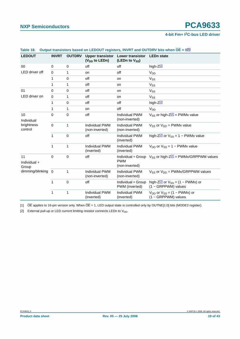
7.3.6 LED driver output state, LEDOUT
LDRx = 00 — LED driver x is off (default power-up state).
LDRx = 01 — LED driver x is fully on (individual brightness and group dimming/blinkingnot controlled).
LDRx = 10 — LED driver x individual brightness can be controlled through its PWMxregister.
LDRx = 11 — LED driver x individual brightness and group dimming/blinking can becontrolled through its PWMx register and the GRPPWM registers.
duty cycleGDC 7:0[ ]
256---------------------------=
Table 12. GRPFREQ - Group Frequency register (address 07h) bit descriptionLegend: * default value.
Address Register Bit Symbol Access Value Description
Product data sheet Rev. 05 — 25 July 2008 14 of 43
NXP Semiconductors PCA96334-bit Fm+ I 2C-bus LED driver
7.3.7 I2C-bus subaddress 1 to 3, SUBADRx
Subaddresses are programmable through the I2C-bus. Default power-up values are E2h,E4h, E8h, and the device(s) will not acknowledge these addresses right after power-up(the corresponding SUBx bit in MODE1 register is equal to 0).
Once subaddresses have been programmed to their right values, SUBx bits need to beset to 1 in order to have the device acknowledging these addresses (MODE1 register).
Only the 7 MSBs representing the I2C-bus subaddress are valid. The LSB in SUBADRxregister is a read-only bit (0).
When SUBx is set to 1, the corresponding I2C-bus subaddress can be used during eitheran I2C-bus read or write sequence.
7.3.8 LED All Call I 2C-bus address, ALLCALLADR
The LED All Call I2C-bus address allows all the PCA9633s in the bus to be programmedat the same time (ALLCALL bit in register MODE1 must be equal to 1, power-up defaultstate). This address is programmable through the I2C-bus and can be used during eitheran I2C-bus read or write sequence. The register address can be programmed as asub call.
Only the 7 MSBs representing the All Call I2C-bus address are valid. The LSB inALLCALLADR register is a Read-only bit (0).
If ALLCALL bit = 0, the device does not acknowledge the address programmed in registerALLCALLADR.
Table 14. SUBADR1 to SUBADR3 - I 2C-bus subaddress registers 0 to 3 (address 09h to0Bh) bit description
Legend: * default value.
Address Register Bit Symbol Access Value Description
Product data sheet Rev. 05 — 25 July 2008 15 of 43
NXP Semiconductors PCA96334-bit Fm+ I 2C-bus LED driver
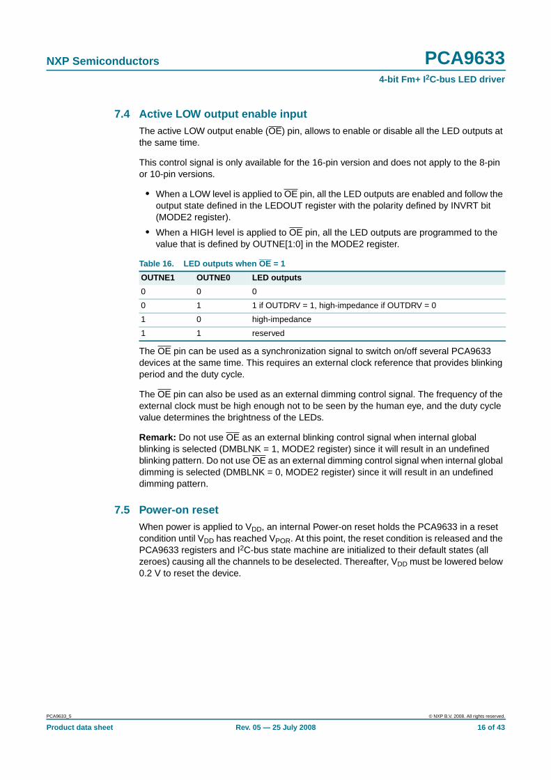
7.4 Active LOW output enable inputThe active LOW output enable (OE) pin, allows to enable or disable all the LED outputs atthe same time.
This control signal is only available for the 16-pin version and does not apply to the 8-pinor 10-pin versions.
• When a LOW level is applied to OE pin, all the LED outputs are enabled and follow theoutput state defined in the LEDOUT register with the polarity defined by INVRT bit(MODE2 register).
• When a HIGH level is applied to OE pin, all the LED outputs are programmed to thevalue that is defined by OUTNE[1:0] in the MODE2 register.
The OE pin can be used as a synchronization signal to switch on/off several PCA9633devices at the same time. This requires an external clock reference that provides blinkingperiod and the duty cycle.
The OE pin can also be used as an external dimming control signal. The frequency of theexternal clock must be high enough not to be seen by the human eye, and the duty cyclevalue determines the brightness of the LEDs.
Remark: Do not use OE as an external blinking control signal when internal globalblinking is selected (DMBLNK = 1, MODE2 register) since it will result in an undefinedblinking pattern. Do not use OE as an external dimming control signal when internal globaldimming is selected (DMBLNK = 0, MODE2 register) since it will result in an undefineddimming pattern.
7.5 Power-on resetWhen power is applied to VDD, an internal Power-on reset holds the PCA9633 in a resetcondition until VDD has reached VPOR. At this point, the reset condition is released and thePCA9633 registers and I2C-bus state machine are initialized to their default states (allzeroes) causing all the channels to be deselected. Thereafter, VDD must be lowered below0.2 V to reset the device.
Product data sheet Rev. 05 — 25 July 2008 16 of 43
NXP Semiconductors PCA96334-bit Fm+ I 2C-bus LED driver
7.6 Software ResetThe Software Reset Call (SWRST Call) allows all the devices in the I2C-bus to be reset tothe power-up state value through a specific formatted I2C-bus command. To be performedcorrectly, it implies that the I2C-bus is functional and that there is no device hanging thebus.
The SWRST Call function is defined as the following:
1. A START command is sent by the I2C-bus master.
2. The reserved SWRST I2C-bus address ‘0000 011’ with the R/W bit set to 0 (write) issent by the I2C-bus master.
3. The PCA9633 device(s) acknowledge(s) after seeing the SWRST Call address‘0000 0110’ (06h) only. If the R/W bit is set to 1 (read), no acknowledge is returned tothe I2C-bus master.
4. Once the SWRST Call address has been sent and acknowledged, the master sends2 bytes with 2 specific values (SWRST data byte 1 and byte 2):
a. Byte 1 = A5h: the PCA9633 acknowledges this value only. If byte 1 is not equal toA5h, the PCA9633 does not acknowledge it.
b. Byte 2 = 5Ah: the PCA9633 acknowledges this value only. If byte 2 is not equal to5Ah, then the PCA9633 does not acknowledge it.
If more than 2 bytes of data are sent, the PCA9633 does not acknowledge any more.
5. Once the right 2 bytes (SWRST data byte 1 and byte 2 only) have been sent andcorrectly acknowledged, the master sends a STOP command to end the SWRST Call:the PCA9633 then resets to the default value (power-up value) and is ready to beaddressed again within the specified bus free time (tBUF).
The I2C-bus master must interpret a non-acknowledge from the PCA9633 (at any time) asa ‘SWRST Call Abort’. The PCA9633 does not initiate a reset of its registers. Thishappens only when the format of the SWRST Call sequence is not correct.
Product data sheet Rev. 05 — 25 July 2008 17 of 43
NXP Semiconductors PCA96334-bit Fm+ I 2C-bus LED driver
7.7 Using the PCA9633 with and without external driversThe PCA9633 LED output drivers are 5.5 V only tolerant and can sink up to 25 mA at 5 V.
If the device needs to drive LEDs to a higher voltage and/or higher current, use of anexternal driver is required.
• INVRT bit (MODE2 register) can be used to keep the LED PWM control firmware thesame (PWMx and GRPPWM values directly calculated from their respective formulasand the LED output state determined by LEDOUT register value) independently of thetype of external driver. This bit allows LED output polarity inversion/non-inversion onlywhen OE = 0.
• OUTDRV bit (MODE2 register) allows minimizing the amount of external componentsrequired to control the external driver (N-type or P-type device).
[1] OE applies to 16-pin version only. When OE = 1, LED output state is controlled only by OUTNE[1:0] bits (MODE2 register).
[2] Correct configuration when LEDs directly connected to the LEDn outputs (connection to VDD through current limiting resistor).
[3] Optimum configuration when external N-type (NPN, NMOS) driver used.
[4] Optimum configuration when external P-type (PNP, PMOS) driver used.
Table 17. Use of INVRT and OUTDRV based on connection to the LEDn outputs when OE = 0[1]
INVRT OUTDRV Direct connection to LEDn External N-type driver External P-type driver
Firmware Externalpull-upresistor
Firmware Externalpull-upresistor
Firmware Externalpull-upresistor
0 0 formulas and LEDoutput state valuesapply[2]
LED currentlimiting R[2]
formulas and LEDoutput statevalues inverted
required formulas and LEDoutput state valuesapply
required
0 1 formulas and LEDoutput state valuesapply[2]
LED currentlimiting R[2]
formulas and LEDoutput statevalues inverted
not required formulas and LEDoutput state valuesapply[4]
notrequired[4]
1 0 formulas and LEDoutput state valuesinverted
LED currentlimiting R
formulas and LEDoutput statevalues apply
required formulas and LEDoutput state valuesinverted
Product data sheet Rev. 05 — 25 July 2008 19 of 43
NXP Semiconductors PCA96334-bit Fm+ I 2C-bus LED driver
7.8 Individual brightness control with group dimming/blinkingA 97 kHz fixed frequency signal with programmable duty cycle (8 bits, 256 steps) is usedto control individually the brightness for each LED.
On top of this signal, one of the following signals can be superimposed (this signal can beapplied to the 4 LED outputs):
• A lower 190 Hz fixed frequency signal with programmable duty cycle (8 bits,256 steps) is used to provide a global brightness control.
• A programmable frequency signal from 24 Hz to 1⁄10.73 Hz (8 bits, 256 steps) withprogrammable duty cycle (8 bits, 256 steps) is used to provide a global blinkingcontrol.
Minimum pulse width for LEDn Brightness Control is 40 ns.
Minimum pulse width for Group Dimming is 20.48 µs.
When M = 1 (GRPPWM register value), the resulting LEDn Brightness Control + Group Dimming signal will have 2 pulses ofthe LED Brightness Control signal (pulse width = N × 40 ns, with ‘N’ defined in PWMx register).
This resulting Brightness + Group Dimming signal above shows a resulting Control signal with M = 4 (8 pulses).
Product data sheet Rev. 05 — 25 July 2008 20 of 43
NXP Semiconductors PCA96334-bit Fm+ I 2C-bus LED driver
8. Characteristics of the I 2C-bus
The I2C-bus is for 2-way, 2-line communication between different ICs or modules. The twolines are a serial data line (SDA) and a serial clock line (SCL). Both lines must beconnected to a positive supply via a pull-up resistor when connected to the output stagesof a device. Data transfer may be initiated only when the bus is not busy.
8.1 Bit transferOne data bit is transferred during each clock pulse. The data on the SDA line must remainstable during the HIGH period of the clock pulse as changes in the data line at this timewill be interpreted as control signals (see Figure 12).
8.1.1 START and STOP conditions
Both data and clock lines remain HIGH when the bus is not busy. A HIGH-to-LOWtransition of the data line while the clock is HIGH is defined as the START condition (S). ALOW-to-HIGH transition of the data line while the clock is HIGH is defined as the STOPcondition (P) (see Figure 13).
8.2 System configurationA device generating a message is a ‘transmitter’; a device receiving is the ‘receiver’. Thedevice that controls the message is the ‘master’ and the devices which are controlled bythe master are the ‘slaves’ (see Figure 14).
Product data sheet Rev. 05 — 25 July 2008 21 of 43
NXP Semiconductors PCA96334-bit Fm+ I 2C-bus LED driver
8.3 AcknowledgeThe number of data bytes transferred between the START and the STOP conditions fromtransmitter to receiver is not limited. Each byte of eight bits is followed by oneacknowledge bit. The acknowledge bit is a HIGH level put on the bus by the transmitter,whereas the master generates an extra acknowledge related clock pulse.
A slave receiver which is addressed must generate an acknowledge after the reception ofeach byte. Also a master must generate an acknowledge after the reception of each bytethat has been clocked out of the slave transmitter. The device that acknowledges has topull down the SDA line during the acknowledge clock pulse, so that the SDA line is stableLOW during the HIGH period of the acknowledge related clock pulse; set-up time and holdtime must be taken into account.
A master receiver must signal an end of data to the transmitter by not generating anacknowledge on the last byte that has been clocked out of the slave. In this event, thetransmitter must leave the data line HIGH to enable the master to generate a STOPcondition.
Product data sheet Rev. 05 — 25 July 2008 25 of 43
NXP Semiconductors PCA96334-bit Fm+ I 2C-bus LED driver
10. Application design-in information
Question 1: What kind of edge rate control is there on the outputs?
• The typical edge rates depend on the output configuration, supply voltage, and theapplied load. The outputs can be configured as either open-drain NMOS or totem poleoutputs. If the customer is using the part to directly drive LEDs, they should be using itin an open-drain NMOS, if they are concerned about the maximum ISS and groundbounce. The edge rate control was designed primarily to slow down the turn-on of theoutput device; it turns off rather quickly (~1.5 ns). In simulation, the typical turn-ontime for the open-drain NMOS was ~14 ns (VDD = 3.6 V; CL = 50 pF; RPU = 500 Ω).
Question 2: Is ground bounce possible?
• Ground bounce is a possibility, especially if all 16 outputs are changed at full current(25 mA each). There is a fair amount of decoupling capacitance on chip (~50 pF),which is intended to suppress some of the ground bounce. The customer will need todetermine if additional decoupling capacitance externally placed as close asphysically possible to the device is required.
I2C-bus address = 0010 101X.
All of the 4 LEDn outputs configurable as either open-drain or totem pole. Mixing of configurations is not possible.
(1) OE requires pull-up resistor if control signal from the master is open-drain.
Product data sheet Rev. 05 — 25 July 2008 26 of 43
NXP Semiconductors PCA96334-bit Fm+ I 2C-bus LED driver
Question 3: Can I really sink 400 mA through the single ground pin on the package andwill this cause any ground bounce problem due to the PWM of the LEDs?
• Yes, you can sink 400 mA through a single ground pin on the package . Although thepackage only has one ground pin, there are two ground pads on the die itselfconnected to this one pin. Although some ground bounce is likely, it will not disrupt theoperation of the part and would be reduced by the external decoupling capacitance.
Question 4: I can’t turn the LEDs on or off, but their registers are set properly. Why?
• Check the Mode Register 1 bit 4 SLEEP setting. The value needs to be 0 so that theOSC is turn on. If the OSC is turned off, the LEDs cannot be turned on or off and alsocan’t be dimmed or blinked.
Question 5: I’m using LEDs with integrated Zener diodes and the IC is getting very hot.Why?
• The IC outputs can be set to either open-drain or push-pull and default to push-pulloutputs. In this application with the Zener diodes, they need to be set to open-drainsince in the push-pull architecture there is a low resistance path to GND through theZener and this is causing the IC to overheat. The PCA9632/33/34/35 ICs all power-upin the push-pull output mode and with the logic state HIGH, so one of the first thingsthat need to be done is to set the outputs to open-drain.
11. Limiting values
Table 19. Limiting valuesIn accordance with the Absolute Maximum Rating System (IEC 60134).
Symbol Parameter Conditions Min Max Unit
VDD supply voltage −0.5 +6.0 V
VI/O voltage on an input/output pin VSS − 0.5 5.5 V
Product data sheet Rev. 05 — 25 July 2008 28 of 43
NXP Semiconductors PCA96334-bit Fm+ I 2C-bus LED driver
[1] VDD must be lowered to 0.2 V in order to reset part.
[2] Each bit must be limited to a maximum of 25 mA and the total package limited to 100 mA due to internal busing limits.
13. Dynamic characteristics
[1] Minimum SCL clock frequency is limited by the bus time-out feature, which resets the serial bus interface if either SDA or SCL is heldLOW for a minimum of 25 ms. Disable bus time-out feature for DC operation.
[2] tVD;ACK = time for Acknowledgement signal from SCL LOW to SDA (out) LOW.
[3] tVD;DAT = minimum time for SDA data out to be valid following SCL LOW.
[4] Cb = total capacitance of one bus line in pF.
Address inputs
VIL LOW-level input voltage −0.5 - +0.3VDD V
VIH HIGH-level input voltage 0.7VDD - 5.5 V
ILI input leakage current −1 - +1 µA
Ci input capacitance - 3.7 5 pF
Table 20. Static characteristics …continuedVDD = 2.3 V to 5.5 V; VSS = 0 V; Tamb = −40 °C to +85 °C; unless otherwise specified.
Product data sheet Rev. 05 — 25 July 2008 29 of 43
NXP Semiconductors PCA96334-bit Fm+ I 2C-bus LED driver
[5] A master device must internally provide a hold time of at least 300 ns for the SDA signal (refer to the VIL of the SCL signal) in order tobridge the undefined region of SCL’s falling edge.
[6] The maximum tf for the SDA and SCL bus lines is specified at 300 ns. The maximum fall time (tf) for the SDA output stage is specified at250 ns. This allows series protection resistors to be connected between the SDA and the SCL pins and the SDA/SCL bus lines withoutexceeding the maximum specified tf.
[7] Input filters on the SDA and SCL inputs suppress noise spikes less than 50 ns.
Product data sheet Rev. 05 — 25 July 2008 37 of 43
NXP Semiconductors PCA96334-bit Fm+ I 2C-bus LED driver
16. Handling information
Inputs and outputs are protected against electrostatic discharge in normal handling.However, to be completely safe you must take normal precautions appropriate to handlingintegrated circuits.
17. Soldering of SMD packages
This text provides a very brief insight into a complex technology. A more in-depth accountof soldering ICs can be found in Application Note AN10365 “Surface mount reflowsoldering description”.
17.1 Introduction to solderingSoldering is one of the most common methods through which packages are attached toPrinted Circuit Boards (PCBs), to form electrical circuits. The soldered joint provides boththe mechanical and the electrical connection. There is no single soldering method that isideal for all IC packages. Wave soldering is often preferred when through-hole andSurface Mount Devices (SMDs) are mixed on one printed wiring board; however, it is notsuitable for fine pitch SMDs. Reflow soldering is ideal for the small pitches and highdensities that come with increased miniaturization.
17.2 Wave and reflow solderingWave soldering is a joining technology in which the joints are made by solder coming froma standing wave of liquid solder. The wave soldering process is suitable for the following:
• Through-hole components
• Leaded or leadless SMDs, which are glued to the surface of the printed circuit board
Not all SMDs can be wave soldered. Packages with solder balls, and some leadlesspackages which have solder lands underneath the body, cannot be wave soldered. Also,leaded SMDs with leads having a pitch smaller than ~0.6 mm cannot be wave soldered,due to an increased probability of bridging.
The reflow soldering process involves applying solder paste to a board, followed bycomponent placement and exposure to a temperature profile. Leaded packages,packages with solder balls, and leadless packages are all reflow solderable.
Key characteristics in both wave and reflow soldering are:
• Board specifications, including the board finish, solder masks and vias
• Package footprints, including solder thieves and orientation
• The moisture sensitivity level of the packages
• Package placement
• Inspection and repair
• Lead-free soldering versus SnPb soldering
17.3 Wave solderingKey characteristics in wave soldering are:
Product data sheet Rev. 05 — 25 July 2008 38 of 43
NXP Semiconductors PCA96334-bit Fm+ I 2C-bus LED driver
• Process issues, such as application of adhesive and flux, clinching of leads, boardtransport, the solder wave parameters, and the time during which components areexposed to the wave
• Solder bath specifications, including temperature and impurities
17.4 Reflow solderingKey characteristics in reflow soldering are:
• Lead-free versus SnPb soldering; note that a lead-free reflow process usually leads tohigher minimum peak temperatures (see Figure 32) than a SnPb process, thusreducing the process window
• Solder paste printing issues including smearing, release, and adjusting the processwindow for a mix of large and small components on one board
• Reflow temperature profile; this profile includes preheat, reflow (in which the board isheated to the peak temperature) and cooling down. It is imperative that the peaktemperature is high enough for the solder to make reliable solder joints (a solder pastecharacteristic). In addition, the peak temperature must be low enough that thepackages and/or boards are not damaged. The peak temperature of the packagedepends on package thickness and volume and is classified in accordance withTable 22 and 23
Moisture sensitivity precautions, as indicated on the packing, must be respected at alltimes.
Studies have shown that small packages reach higher temperatures during reflowsoldering, see Figure 32.
Table 22. SnPb eutectic process (from J-STD-020C)
Package thickness (mm) Package reflow temperature ( °C)
Volume (mm 3)
< 350 ≥ 350
< 2.5 235 220
≥ 2.5 220 220
Table 23. Lead-free process (from J-STD-020C)
Package thickness (mm) Package reflow temperature ( °C)
Product data sheet Rev. 05 — 25 July 2008 41 of 43
NXP Semiconductors PCA96334-bit Fm+ I 2C-bus LED driver
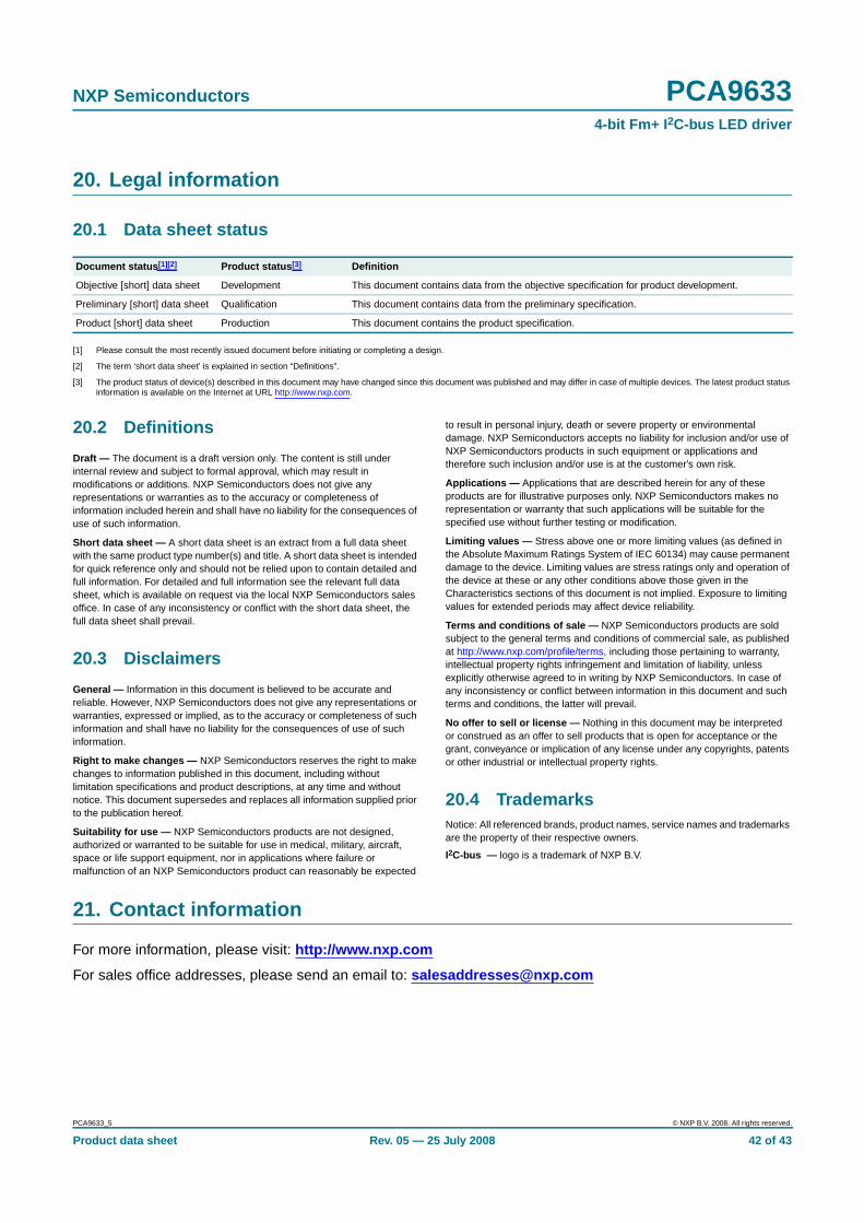
20. Legal information
20.1 Data sheet status
[1] Please consult the most recently issued document before initiating or completing a design.
[2] The term ‘short data sheet’ is explained in section “Definitions”.
[3] The product status of device(s) described in this document may have changed since this document was published and may differ in case of multiple devices. The latest product statusinformation is available on the Internet at URL http://www.nxp.com.
20.2 Definitions
Draft — The document is a draft version only. The content is still underinternal review and subject to formal approval, which may result inmodifications or additions. NXP Semiconductors does not give anyrepresentations or warranties as to the accuracy or completeness ofinformation included herein and shall have no liability for the consequences ofuse of such information.
Short data sheet — A short data sheet is an extract from a full data sheetwith the same product type number(s) and title. A short data sheet is intendedfor quick reference only and should not be relied upon to contain detailed andfull information. For detailed and full information see the relevant full datasheet, which is available on request via the local NXP Semiconductors salesoffice. In case of any inconsistency or conflict with the short data sheet, thefull data sheet shall prevail.
20.3 Disclaimers
General — Information in this document is believed to be accurate andreliable. However, NXP Semiconductors does not give any representations orwarranties, expressed or implied, as to the accuracy or completeness of suchinformation and shall have no liability for the consequences of use of suchinformation.
Right to make changes — NXP Semiconductors reserves the right to makechanges to information published in this document, including withoutlimitation specifications and product descriptions, at any time and withoutnotice. This document supersedes and replaces all information supplied priorto the publication hereof.
Suitability for use — NXP Semiconductors products are not designed,authorized or warranted to be suitable for use in medical, military, aircraft,space or life support equipment, nor in applications where failure ormalfunction of an NXP Semiconductors product can reasonably be expected
to result in personal injury, death or severe property or environmentaldamage. NXP Semiconductors accepts no liability for inclusion and/or use ofNXP Semiconductors products in such equipment or applications andtherefore such inclusion and/or use is at the customer’s own risk.
Applications — Applications that are described herein for any of theseproducts are for illustrative purposes only. NXP Semiconductors makes norepresentation or warranty that such applications will be suitable for thespecified use without further testing or modification.
Limiting values — Stress above one or more limiting values (as defined inthe Absolute Maximum Ratings System of IEC 60134) may cause permanentdamage to the device. Limiting values are stress ratings only and operation ofthe device at these or any other conditions above those given in theCharacteristics sections of this document is not implied. Exposure to limitingvalues for extended periods may affect device reliability.
Terms and conditions of sale — NXP Semiconductors products are soldsubject to the general terms and conditions of commercial sale, as publishedat http://www.nxp.com/profile/terms, including those pertaining to warranty,intellectual property rights infringement and limitation of liability, unlessexplicitly otherwise agreed to in writing by NXP Semiconductors. In case ofany inconsistency or conflict between information in this document and suchterms and conditions, the latter will prevail.
No offer to sell or license — Nothing in this document may be interpretedor construed as an offer to sell products that is open for acceptance or thegrant, conveyance or implication of any license under any copyrights, patentsor other industrial or intellectual property rights.
20.4 TrademarksNotice: All referenced brands, product names, service names and trademarksare the property of their respective owners.
I2C-bus — logo is a trademark of NXP B.V.
21. Contact information
For more information, please visit: http://www .nxp.com
For sales office addresses, please send an email to: salesad [email protected]
Document status [1] [2] Product status [3] Definition
Objective [short] data sheet Development This document contains data from the objective specification for product development.
Preliminary [short] data sheet Qualification This document contains data from the preliminary specification.
Product [short] data sheet Production This document contains the product specification.