PCB design techniques for lowest-cost EMC compliance: Part 2 by M. K. Armstrong Printed circuit boards (PCBs) are widely used in electronic equipment and systems. Application of good EMC (electromagnetic compatibility) practices t o their design usually helps to achieve compliance with EMC regulations at much lower cost than alternative EMC measures at higher levels of integration, and also improves signal integrity. This, the second part of the paper discusses in detail techniques for improving the power supply of a PCB and using transmission lines. 1 Introduction Part 1 ofthis paper discussed how the techniques of circuit segregation, interface suppression and the use of ground and power planes can be applied to printed circuit boards (PCBs) to help improve the EMC (electromagnetic compatibility) performance of electronic equipment and systems. Part 2 discusses two further techniques: power decoupling and the use of transmission lines. These five ‘best-practice’ EMC techniques interact with each other to give dramatic improvements in the EMC of electronic circuits which use PCBs. 2 Power decoupling This technique must be considered as a part of the circuit design process itself, as well as part of the PCB layout. The aim of power decoupling, crudely put, is to maintain the power supply impedance to each IC on the PCB to 1 R or less across the entire frequency range of interest for EMC (at least 150 kHz to 1 GHz). Some high-speed or powerful ICs may require a power supply impedance of 0.1 P or less over certain frequency ranges for correct operation. Wires and PCB tracks all have much too much inductance to provide such low impedances. Decoupling a power rail means connecting capacitors between it and its respective ground (0 V) reference. Correct power decoupling keeps current loops in power supply circuits small, thereby reducing inductive ahd common impedance coupling. It also keeps the voltage fluctuations on power rails low, reducing capacitive coupling. Also, the functional operationsof most digital ICs (especially those using higher clock speeds) can depend critically upon the high-frequency performance of their power supplies. Power decoupling techniques A large decoupling capacitor (e.g. 100 pF) should be fitted at every point where power supplies enter (or leave) the PCB, and some smaller capacitors (e.g. 10 pF tantalum or solid aluminium types) should be ‘sprinkled‘around the PCB on a ‘microfaradper unit area’ principle, e.g. one such tantalumcapacitorfor every nine square inches (58 cm? of PCB, aswell as being positioned near to heavy power users such as microprocessors, memory, and other VLSI ICs; they should also be fitted at every point where power enters or leaves the PCB. These capacitors will help to control lower frequencies, say up to 10 MUz. The power supplies to every IC should be decoupled very close to the device concerned (and to every transistor connected to a power rail), using appropriate capacitor sizes and types (see later). Where an IC has a number of power pins of the same type (e.g.VcJ , each should have an appropriate decoupling capacitor mounted as close as possible to it. Achieving good decouplingperformance above 10 MHz is more difficult as the frequency increases, because the inductances of component leads, PCB tracks, via holes, and capacitor self-inductance inevitably limit the KF performance. The achievement of good power supply decoupling at higher frequencies using capacitors mounted close to IC power pins is discussed next. Determining the values of the local decouplingcapaciiorsfor each IC The total local decouplimg capacitance required for an IC depends on its transient current demands and the power supply’svoltage tolerances. VLSI (very large scale IC) and RAM (random access memory) manufacturers should be able to specify the values (and maybe even the capacitor types and preferred layoutpatterns) for their products, but 218 ELECTRONICS & COMMUNICATIONENGINEERING JOURNAL OCTOBER 1999
Transcript
PCB design techniques for lowest-cost EMC
compliance: Part 2 by M. K. Armstrong
Printed circuit boards (PCBs) are widely used in electronic equipment and systems. Application of good E M C (electromagnetic compatibility) practices t o their design usually helps to achieve compliance with E M C regulations at much lower cost than alternative E M C measures a t higher levels of integration, and also improves signal
integrity. This, the second part of the paper discusses in detail techniques for improving the power supply of a PCB and using transmission lines.
1 Introduction
Part 1 ofthis paper discussed how the techniques of circuit segregation, interface suppression and the use of ground and power planes can be applied to printed circuit boards (PCBs) to help improve the EMC (electromagnetic compatibility) performance of electronic equipment and systems. Part 2 discusses two further techniques: power decoupling and the use of transmission lines. These five ‘best-practice’ EMC techniques interact with each other to give dramatic improvements in the EMC of electronic circuits which use PCBs.
2 Power decoupling
This technique must be considered as a part of the circuit design process itself, as well as part of the PCB layout. The aim of power decoupling, crudely put, is to maintain the power supply impedance to each IC on the PCB to 1 R or less across the entire frequency range of interest for EMC (at least 150 kHz to 1 GHz). Some high-speed or powerful ICs may require a power supply impedance of 0.1 P or less over certain frequency ranges for correct operation. Wires and PCB tracks all have much too much inductance to provide such low impedances.
Decoupling a power rail means connecting capacitors between it and its respective ground (0 V) reference. Correct power decoupling keeps current loops in power supply circuits small, thereby reducing inductive ahd common impedance coupling. It also keeps the voltage fluctuations on power rails low, reducing capacitive coupling. Also, the functional operations of most digital ICs (especially those using higher clock speeds) can depend critically upon the high-frequency performance of their power supplies.
Power decoupling techniques A large decoupling capacitor (e.g. 100 pF) should be
fitted at every point where power supplies enter (or leave) the PCB, and some smaller capacitors (e.g. 10 pF tantalum or solid aluminium types) should be ‘sprinkled‘ around the PCB on a ‘microfarad per unit area’ principle, e.g. one such tantalum capacitor for every nine square inches (58 cm? of PCB, aswell as being positioned near to heavy power users such as microprocessors, memory, and other VLSI ICs; they should also be fitted at every point where power enters or leaves the PCB. These capacitors will help to control lower frequencies, say up to 10 MUz.
The power supplies to every IC should be decoupled very close to the device concerned (and to every transistor connected to a power rail), using appropriate capacitor sizes and types (see later). Where an IC has a number of power pins of the same type (e.g. VcJ , each should have an appropriate decoupling capacitor mounted as close as possible to it.
Achieving good decoupling performance above 10 MHz is more difficult as the frequency increases, because the inductances of component leads, PCB tracks, via holes, and capacitor self-inductance inevitably limit the KF performance. The achievement of good power supply decoupling at higher frequencies using capacitors mounted close to IC power pins is discussed next.
Determining the values of the local decouplingcapaciiorsfor each IC
The total local decouplimg capacitance required for an IC depends on its transient current demands and the power supply’s voltage tolerances. VLSI (very large scale IC) and RAM (random access memory) manufacturers should be able to specify the values (and maybe even the capacitor types and preferred layout patterns) for their products, but
218 ELECTRONICS & COMMUNICATION ENGINEERING JOURNAL OCTOBER 1999
note that they will probably have assumed an accurate 5 V power supply, not always achieved in real life.
To calculate the value of decoupling capacitance required for an IC, use the formula C(A@ = I(At), using the units farads, volts, amps, and seconds.
In this formula, AVis the available tolerance on the IC‘s power supply voltage, derived by subtracting the IC‘s minimum supply voltage specification for correct operation (from its data sheet) from the minimum power supply voltage (takng account of all the tolerances, regulation parameters, and the voltage drops due to the resistance of the power conductors). This calculation should be done for the worst case operational temperatures, and should take into account temperature and ageing coefficients of the power supply regulators and theirloadregulationcurves. AVoftenturnsouttobeamere +lo0 mV. (A negative figure would indicate potential problems with reliability in the field.)
I is the IC‘s transient current demand from its power supplies, which lasts for the time At. For many modem digital ICs, At is 2 ns or even less and may be assumed to be the same as the specified low-high or high-low transition times for the digital outputs. I is a parameter almost never provided by device manufacturers. It will usually be estimated or measured in some reasonably sensible way. For many digital devices the output current cannot be used for I because their ‘shoot-through‘ currents (caused by overlapping conduction in totem-pole output stages) are more significant. (Shoot-through currents are also known by other names, such as ‘transient supply current‘.) These can be an order of magnitude higher than the IC‘s transient output currents into its capacitive load, although they usually only last for a fraction of the output’s transition times.
In the absence of IC manufacturer’s data detailing power supply current versus time data, or giving detailed power supply decoupling specifications, a very high-speed two-channel oscilloscope may be used to measure both I and At. Two probes should be used in A-B mode to measure the voltage across a low- value SMD (surface mount device) resistor inserted into the power supply of the IC concerned (SMD resistors behave as a resistor up to 1 GHz at least). The value of the resistor should be such that the peak voltage measured across the resistor by the A-B probes is no more than +lo0 mV, and the resistor should be positioned between the IC‘s power pins and its PCB-mounted decoupling capaci- tors. Some larger ICs, such as the PentiumTM, may not operate properly if the resistor or its lead lengths are not kept so short that a magnifying glass is needed to solder them in place. For the
Pentium IC, good-quality data on its transient current demands are provided by its manufacturer, Intel. There is nopointinbyiugtomeasureIand Atto anaccuracygreater than d o % , since this tolerance is less than the typical value tolerance of decoupling capacitor components.
Where AVvalues are low, and decoupling capacitance needs to be correspondinglyhigh, it can be cost-effective to improve the regulation of the power supply, and the resistance ofits PCB connections, to increase AVand allow the use of smaller decoupling capacitance near to each IC. This can also help achieve the desired EMC, due to the higher self-resonance frequencies of smaller capacitors.
Self-resonance limitations in capacitots The typical capacitor value resulting from the above
calculation is often in the 1-10 nF region for small- or medium-scale integrated ‘glue logic’ ICs and ECL (emitter coupled logic), and often 100 nF or more for VLSI devices such as microprocessors, memory ICs and gate arrays.
Unfortunately, self-resonance in capacitors prevents them from providing a low impedance at high frequencies. As their capacitance value increases, the highest frequency at which they remain useful decreases. The first (series) resonant frequency (SRF) of a capacitor depends upon its internal inductance (equivalent series inductance, or ESL), the inductance of its leads, and the inductance of any tracks and vias it is connected to. A first-order approximation for capacitor SRF is given by:
f;,= 1 / ( 2 n G ) (1)
where L = ESL (internal to the capacitor) + the total inductance of any leads + the total inductance of any tracks and/or vias. The rule-of-thumb is to assume 1 nH/mm for any leads and/or tracks between the capacitor’s body and the power pins of the IC to be decoupled. Via holes are
Fig. 1 Series resonances in decoupling capacitor (guide only). MLC = multilayer ceramic; SMD =surface mount device
ELECTRONICS & COMMUNICATION ENGINEERING JOURNAL OCTOBER 1999 219
imoedance of 100 nF +'I nF combinalion.
showing parallel 1 nF SMD MLC with no track , resonance i o0 "F SMD MLC
0.1 0.3 1 3 IO 30 100 300 1000
Fig. 2 Example of a parallel resonance between one 100 nF and one 1 nF decoupling capacitor (guide only)
assumed to have 1 nH per millimetre of depth. The inductance contributed by ground and power planes may be neglected (but only when the decoupling capacitor is closetoitsIC).Whenaviaholeconnectsatracktoaplane, only the depth from track to plane is counted.
Decoupling capacitors generally become ineffective at more than 3 times their SRF, as shown by Fig. 1. Reference 2 shows that the best cost-effectiveness is achieved when very careful attention is paid to the inductance of the decoupling capacitors and their connections to the planes. The use of SMD capacitors with low-inductance connections, as shown by Fig. 4 of Part 1 of this paper', is clearly very important for effective (and cost-effective) decoupling.
The capacitor created by the close proximity of ground and power planes (on adjacent PCB layers) has low internal and connection inductance and can provide low decoupling impedance to above 1 GHz. For example, ground and power planes in PCBs made from FR4 glass fibre material, with 0.15 mm separation, create approximately 23 pF/cm2 of high-quality RF capacitance.
Good decoupling performance at frequencies from 10 to 1000 MHz is therefore hest achieved by combining the intrinsic capacitance of adjacent ground and power planes with short-leaded multilayer ceramic (MLC) capacitors (preferably SMD types) mounted close to each of the power pins of every IC (or transistor). At least one company offers a PCB process that uses special dielectric materials between adjacent ground and power planes to increase the interplane capacitance and allow many of the smaller decoupling capacitors to be eliminated.
Threeterminal and 'feedthrough' types of SMD decoupling capacitor exist and have a much higher SRF than the regular two-terminal capacitors. However, they are expensive and may not allow the lowest-inductance connection to thepowerplane, so shouldbeusedwith care. There are also laminar capacitor devices (such as the Micro/Q range) made to fit under leaded ICs; these are also expensive and seem to be used mostly for improving
the EMC of existing PCBs without resorting to redesign.
Combining decoupling capacitors - problems with parallel resonances
When two decoupling capacitors are provided on a PCB, a parallel (high impedance) resonance is created in between their individual series resonant frequencies, as shown by Fig. 2 . This high impedance prevents the achievement of good EMC at that frequency (and close to it).
This problem is more likely to occur on PCBs with only a few ICs and hence only a few decoupling capacitors, and in these cases should be controlled by fitting a small-value resistor, such as 1 R, or a small ferrite bead (preferably using SMD packages and short tracks) in series with one of the leads on the
larger value capacitors. When a large number of decoupling capacitors (say over
30) are spread over a ground/power plane PCB, the resulting multiple parallel resonances are swamped by the multiple series resonances. The impedance of the supply is effectively maintained at a low level across a very wide frequency range'.
Although the capacitance between close proximity ground/power planes is intrinsically nonresonant (at least to 1 GHz), ground and power planes do in fact exhibit resonance due to their dimensions. High-frequency currents in the planes suffer strong reflections at their edges, and their ricocheting from side to side of the PCB makes the planes resonant, with effects in the frequency domain similar to series and parallel resonances in capacitors. However, this is not a reason for avoiding ground/power planes, as the time domain analysis below shows.
The rate at which discrete component capacitors can provide current (di/dt) is limited by their internal inductance, and it is very difficult to get any current even from low-value SMD MLC types during the first nanosecond or two of a transient current demand. But ground/power plane combinations have extremely low internal inductances and so can provide current very rapidly, say for the first nanosecond of a transient demand.
Fig. 3 shows a time domain view of effective power supply decoupling. The first nanosecond or so of an IC's transient power current demand can only be provided by its local ground/power plane capacitance, the current demand from 1 to 3 ns being provided by the small value MIL capacitors (up to 10 nF) which are located within 20 mm or so of the IC's power pins, with larger or further away capacitors (>lo0 nF) only being able to contribute significantly to the current demand from the IC after at least 3 ns.
'Bulk' capacitors (such as tantalums) can only begin to provide significant current after 20 ns or more, even ifthey are nearby. Nonceramic dielectric and aluminium
220 ELECTRONICS & COMMUNICATION ENGINEERING JOURNAL OCTOBER 1999
electrolytic capacitors can be slower in their response to a current demand than might be expected from their frequency- domain behaviour, due to a phenomenon known as dielectric absorption, or dielectric memory (another reason for using ceramic capacitors for high-frequency decoupling) .
Ground/power plane capaci- tance is essential to maintain low power-supply impedance, even though it does create resonances in the frequency domain which need to be controlled for good EMC. For low power-supply impedance up to 1 GHz, which is increasingly necessary as clock speeds exceed 100 MHz, the addition of very low-
I example of an ICs pawer sypply current demand
0 1 2 3 4 5 time, ns
Fig. 3 A time domain view of correct power supply decoupling
value decoupling capacitors, typically in the hundreds of picofarads range, may be necessary. (100 pF capacitors with SRFs of 1 GHz are available from some manufacturers.)
PCB layer 'stack up' Considering the above, it is best EMC practice to
provide ground and power planes on adjacent layers in a PCB, and to maximise their capacitance by using only a thin dielectric (say 0.15 mm) between them. In multilayer boards with more than one ground plane, at least one ground/power plane combination should be provided.
Where there are a number of different power supplies, there may need to be a number of different power planes, each on an adjacent layer to a ground plane. Due to the careful segregation of circuits described in part 1 of this paper', it is usually possible to have several power planes on the same PCB layer, e.g. for digital +5 V and +3.3 V supplies, and analogue *12 V supplies.
A four-layer PCB thus bas its layers arranged as follows: 1: signal; 2: ground; 3: power; 4 signal -with the ground and power planes usually separated by only a 0.15 mm thickness of glass-fibre. Highest-speed or most- sensitive tracks should he routed on the layer closest to the ground plane, whereas more indifferent tracks should be routed on the side closest to the power plane. High-speed clocks and data busses, and similarly aggressive tracks, should not swap layers. Highest- speed signals may need to use transmission-line techniques, described in Section 3. Where more signal layers are required, the ground and power plane 'core' should be retained and additional signal layers added. If additional ground planes are not added, the extra tracking layers should only carry signals which are
1: ground 2 signal 3 signal 4 ground 1: signal 2 ground 3 signal 4 ground 1: ground 2 signal 3 signal 4 ground
unlikely to cause EMC problems. In modem high-power computing products almost all
the digital tracks are considered aggressive, and there are so many tracks that two tracking layers are often insufficient. For these it is often best to go straight from a four-layer to an eight-layer board, making sure that every signaltrackinglayer runsclose to aground orpower plane. With a total of three ground plane layers needed to ensure that each signal layer has an adjacent plane, and retaining a ground/power pair for decoupling, an Rlayer stack-up for a computer motherboard may be made as shown at the bottom of the page.
To help prevent crosstalk between adjacent signal layers, they should be routed with their tracks at 90" to each other (horizontal andvertical). Having ground planes on the outer layers (as in the first stack-up above) can provide the greatestbenefitsfor EMC byreducingexternal coupling to inner tracks. Reference 3 makes a different case for the benefits of having a ground plane layer on the active component side of high-speed PCBs.
Further improving decoupling perfmance and cost- effectiveness
To achieve a low power-supply impedance over the whole frequency range of interest, it is necessary to combine various values of decoupling capacitance with the power/gronnd plane capacitance, according to the needs of the circuit. Where two decoupling capacitors are required at an IC's power pin, the smallestvalue should be mounted closest to the pin.
When a product with digital clocks or other frequencies of under 100 MHz is tested for EMC all the decoupling capacitors with values below 1 nF could be left out at first. If they are needed after all this will he revealed by high levels of emissions above 300 MHz, and
5: power 6 signal 7: signal 8: ground 5: power 6 signal 7 ground 8: signal 5: power 6 signal 7: ground 8: signal
ELECTRONICS & COMMUNICATION ENGINEERING JOURNAL OCTOBER 1999 221
they may then be added to the PCB. This is a much better approach than discovering that emissions are too high and only then trying to squeeze a number of additional decoupling capacitors onto the PCB, close to IC power pins.
Ceramic capacitors which employ a COG or NPO dielectric (rather than X7R, Z5U, Y5V, or any of the other standard ceramic dielectric materials) will generally have superior performance at higher frequencies and should always (at the very least) be used for decoupling capacitors of less than 1 nF. Capacitors for which SRF and/or ESL data are provided are preferred over those which do not have these parameters specified.
Devices which have to operate at very high rates or frequencies (say above 200 MHz) may benefit from having their own small area of power plane separated by a 'moat' from the rest of the power plane for their segregated area. This dedicated power plane is supplied from the main power plane through a ferrite bead, forming a segregated high-speed area within an existing circuit area. The high-speed IC's local decoupling capacitors are connected between this small plane and the ground plane (which is common with the rest of their segregated circuit area) and a tantalum decoupling capacitor of 1-10 pF should also he provided. The aim is to increase the 'dimensional' resonant frequency of the IC's local ground/power plane combination until it is so high as to have no deleterious effects. Using this technique in practice may not he easy. It will he necessary to ensure that the small power plane does not suffer parallel resonances at a few 100 MHz due to the low number or variety of decoupling capacitors. Also, all the tracks interconnecting the small plane area to other areas should be routed on the PCB layer adjacent to the continuous ground plane, and any routed next to the power layers at the point where they cross the break.
To get the very best from decoupling, the latest research shows that positioning the relevant ground and power planes closer to the capacitors (and the ICs they decouple) reduces their connection inductance and raises their resonant f req~encies~ .~ . Improving emissions by intentionally tailoring the SRF of decoupling capacitors to correspond to the worst-case frequencies is reported in Reference 5. Reference 6 recommends that, once each IC (or other device) is decoupled locally, additional benefits may be realised by positioning additional low-value decoupling capacitors around the perimeter of the power plane.
No powerplane One way to achieve possibly adequate decoupling
without using a power plane is to connect the power end of each IC's decoupling capacitor(s) directly to the power pin($ of the IC, and then to power the IC from its power rail through a (suitably rated) ferrite bead connected to the power end of the decoupling capacitor. This technique requires a ground plane, so it is suitable for use with double-sided PCBs where all the signal and power tracks have been routed onto one side, leaving the other side for a ground plane. Where a large number of
ferrite beads is required, multilayer hoards may prove to be more cost-effective and require less area.
3 Transmission lines
The transmission-line technique must be considered as a part of the circuit design process itself, as well as part of the PCBlayout.
Introduction to transmission lines Transmission lines are interconnections which maintain
a chosen characteristic impedance (2,) all the way from signal source to load. They have the lowest electric and magoetic field coupling of any interconnections, and unlike all other interconnections do not resonate, however long they are. Transmission lines can easily be made on PCBs hy controlling their materials and dimensions and providing accurate termination resistances at source and/or load. They may be extended off the PCB (i necessary) by commonly available controlled-impedance cables and connectors. Transmission lines are needed for signal integrity when a PCB track is so long that a signal travelling along it cannot, due to its finite velocity of propagation, maintain the same potential at all points along its path. In FR4 dielectric the velocity of propagation of a signal is roughly 60% of the free space value of 3x10' m/s (the speed of light in vacuum). A rule of thumb has grown up in the digital community that PCB tracks need only be treated using transmission-line techniques when the connection length is greater than h/7 at the maximum frequency of interest,f; calculated from:
f= 0.35/t (2)
where tis the faster of the signal's rise and fall times. From a time domain point of view this is roughly the same as saying that transmission-line techniques are required when the time that a digital signal takes to reach the furthest end of its track exceeds half its rise or fall times.
For example, to maintain digital signal integrity for Schottky TTL (transistor-transistor logic) with 3 ns rise times, the maximum frequency of interest is calculated to be 120 MHz, and h/7 at this frequency in FR4 is roughly 180 mm. Using the time domain view, in 3 ns a signal in an FR4 PCB could travel roughly 450 mm, and half of this distance is 225 mm. The frequency domain estimate of 180 mm compares reasonably well with the time domain estimate of 225 mm. Likewise, for 1 ns rise and fall time signals, the corresponding track length (beyond which transmission-line techniques would be required) is 66 mm.
Datahook specifications for output rise or fall times are maximum values, and most devices will switch a lot faster. Another problem is that the capacitive loading created by other devices connected to a signal track slows the propagation velocity below what would be expected just from the dielectric constant of the PCB material (e.g. FR4). Both these effects mean that transmission lines should he used for even shorter lengths of track than the above examples imply, merely
222 ELECTRONICS & COMMUNICATION ENGINEERING JOURNAL OCTOBER 1999
to achieve adequate digital signal integrity. To improve EMC, and to achieve flat analogue-signal frequency response, it is recommended that transmission-line techniques are used when tracks are at most one-half of the length which is found necessary to achieve digital signal integrity. Further improvements in EMC for aggressive PCB tracks (such as digital clocks and data busses) may be possible by using transmission-line techniques on even the shortest tracks.
In most digital designs, transmission lines are generally used for clock distribution and high-speed data busses. They are also used for slower signals that have to travel further, such as on SCSI (small computer system interface) and USB (universal serial bus) interfaces, and also for even slower communications such as l0haseT Ethernet and RS485, which have to be able to remain sufficiently undegraded for very long distances.
IEC 11881-2 : 199S7 gives a wealth of detail on constructing a variety of transmission lines using PCB tracks, plus how to specify their manufacture and check their received qualityon manufactured boards. References 8 and 9 also give very detailed information. Transmission lines are a very large and detailed topic, so this paper will only briefly describe two of the most common types.
The characteristic impedance, Z,, for a surface microstrip (Fig. 4) is given in ohms by’:
87 , / ( E , + 1.41) 0.8E t C Z, = (3)
where e, is the relative permeability of the substrate (typically4.4forFR4 at lOOMHz),Eisthetrackwidth, Cis the thickness of the copper material used, and H is the substrate thickness. The propagation velocity for a surface microstrip is given in nanoseconds per metre as’:
3.335,/(0.4757&, + 0.67) (4)
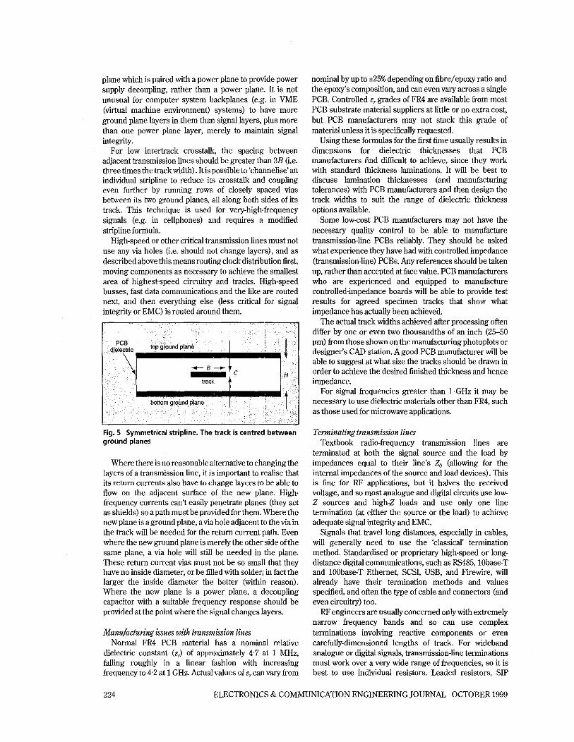
The characteristic impedance of a symmetrical stripline (Fig. 5) is given in ohms by’:
(5)
The propagation velocity for a symmetrical stripline is given in nanoseconds per metre as’:
3.33V&, (6)
Striplinesare slightlyslower thanmicrostrip, but havezero forward crosstalk and much less leakage, i.e. they are better for EMC. Consequently, computer boards and similar circuits with clock rates exceeding 60 MHz or logic transition times of under 5 ns will benefit significantly from the use of stripline, rather than microstrip, for these high- speed signals.
Although striplines are best run between two ground planes, they may also be run between a ground plane and a power plane if the power plane has been correctly decoupled (see Section 2). Breaks in such power
Fig. 4 Surface microstrip
planes must not exist as this would cause sudden changes inZ,.
Compensation for the capacitive loading (typically a few picofarads per gate) can be made to formulas 3,4,5 and 6 as follows:
(7)
from Reference 9, where 2 , is the new (loaded) characteristic impedance, C, is the sum of all capacitive (gate) loads, 2, is the original characteristic impedance (unloaded) of the line, and CO is the original characteristic capacitance of the (unloaded) line obtained from the formulas given in Reference 7. Velocity is slowed according to the formula:
from Reference 9, where Vu is the original (unloaded) and V is the new (loaded) velocity.
It helps transmission-line performance if a uniform rate of ‘gates per unit length’ is maintained, rather than bunching ICs together, although the use of sophisticated CAD (computer-aided design) will allow the line width to be adjusted to maintain the same impedance along its length even when ICs are bunched together.
Different formulas from the ones given here for microstrip and stripline sometimes appear in articles and datahooks, and even in microwave substrate manufacturers’ application notes. The equations given above have been proven over many years to give the correct results and are used by major manufacturers of microwave measuring instruments.
Formulas for coated (or embedded) microstrip, offset striplines, balanced striplines (for balanced signals), and others may be found in References 7 and 8, as well as in many modern PCB CAD packages. Some CAD packages use field solver methods to calcnlateZ,from first principles for evely point along a line -which is much better than relying on choosing the correct formula and hoping that& is not affected too much by proximity to plane edge, proximity to other tracks, use of via holes, capacitive loading by ICs, and accidental errors in layout
The highest-speed (or most susceptible) signals should be run adjacent to a ground plane, preferably a ground
ELECTRONICS & COMMUNICATION ENGINEERING JOURNAL OCTOBER 1999 223
plane which is paired with a power plane to provide power supply decoupling, rather than a power plane. It is not unusual for computer system backplanes (e.g. in VME (virtual machine environment) systems) to have more ground plane layers in them than signal layers, plus more than one power plane layer, merely to maintain signal integrity.
For low intertrack crosstalk, the spacing between adjacent transmission lines should be greater than 3B (i.e. three timesthetrackwidth). Itis possible10 ‘channelise’an individual stripline to reduce its crosstalk and coupling even further by running rows of closely spaced vias between its two ground planes, all along both sides of its track. This technique is used for very-high-frequency signals (e.g. in cellphones) and requires a modified stripline formula.
High-speed or other critical transmission lines must not use any via holes (i.e. should not change layers), and as described above this means routing clockdistribution first, moving components as necessary to achieve the smallest area of highest-speed circuitry and tracks. High-speed busses, fast data communications and the like are routed next, and then everything else (less critical for signal integrity or EMC) is routed around them.
Fig. 5 Symmetrical stripline. The track is centred between ground planes
Where there is no reasonable alternative to changing the layers of a transmission line, it is important to realise that its return currents also have to change layers to be able to flow on the adjacent surface of the new plane. High- frequency currents can’t easily penetrate planes (they act as shields) so a path must be provided for them. Where the newplaneisagroundplane, aviaholeadjacenttotheviain the track will be needed for the return current path. Even where the new ground plane is merely the other side of the same plane, a via hole will still be needed in the plane. These return current vias must not be so small that they have no inside diameter, or be filled with solder; in fact the larger the inside diameter the better (within reason). Where the new plane is a power plane, a decoupling capacitor with a suitable frequency response should be provided at the point where the signal changes layers.
Manufacturing issues with transmission lines Normal FR4 PCB material has a nominal relative
dielectric constant (3 of approximately 4.7 at 1 MHz, falling roughly in a linear fashion with increasing frequency to 4.2 at 1 GHz. Actual values of E, can vary from
224
nominal by up to r25% depending on fibre/epoxy ratio and the epoxy’s composition, and can even vary across a single PCB. Controlled E, grades of FR4 are available from most PCB substrate material suppliers at little or no extra cost, but PCB manufacturers may not stock this grade of material unless it is specifically requested.
Using these formulas for the first time usually results in dimensions for dielectric thicknesses that PCB manufacturers find difficult to achieve, since they work with standard thickness laminations. It will be best to discuss lamination thicknesses (and manufacturing tolerances) with PCB manufacturers and then design the track widths to suit the range of dielectric thickness options available.
Some low-cost PCB manufacturers may not have the necessary quality control to be able to manufacture transmission-line PCBs reliably. They should be asked what experience they have had with controlled impedance (transmission-line) PCBs. Any references should be taken up, rather than accepted at face value. PCB manufacturers who are experienced and equipped to manufacture controlled-impedance boards will be able to provide test results for agreed specimen tracks that show what impedance has actually been achieved.
The actual track widths achieved after processing often differ by one or even two thousandths of an inch (25-50 pm) from those shown on the manufacturing photoplots or designer’s CAD station. Agood PCB manufacturer will be able to suggest at what size the tracks should be drawn in order to achieve the desired finished thickness and hence impedance.
For signal frequencies greater than 1 GHz it may be necessary to use dielectric materials other than FR4, such as those used for microwave applications.
Terminating transmission lines Textbook radio-frequency transmission lines are
terminated at both the signal source and the load by impedances equal to their line’s Z, (allowing for the internal impedances of the source and load devices). This is fine for RF applications, but it halves the received voltage, and so most analogue and digital circuits use low- Z sources and high-Z loads and use only one line termination (at either the source or the load) to achieve adequate signal integrity and EMC.
Signals that travel long distances, especially in cables, will generally need to use the ‘classical’ termination method. Standardised or proprietary high-speed or long- distance digital communications, such as RS485,lObase-T and lOObase-T Ethernet, SCSI, USB, and Firewire, will already have their termination methods and values specified, and often the type of cable and connectors (and even circuitry) too.
RF engineers are usually concerned onlywith extremely narrow frequency bands and so can use complex terminations involving reactive components or even carefully-dimensioned lengths of track. For wideband analogue or digital signals, transmission-line terminations must work over a very wide range of frequencies, so it is best to use individual resistors. Leaded resistors, SIP
ELECTRONICS & COMMUNICATION ENGINEERING JOURNAL OCTOBER 1999
Classical RF termination Parallel (shunt or load) termination
.... wwer plane
line
ground plane R = Z ,
Series (source) termination
.... power plane
I____- around d a m
line
ground plane R = 4
RC IDarallel termination)
Thdvenin (parallel termination)
R ratio minimises ---I load IC receiver)
parallel R
current consumption
combination = L
I ..... I " .
Fig. 6 Transmission line terminations
(single inline package) and DIP (dual inline package) resistor arrays may be used, but SMD resistors are preferred for their higher frequency performance (e.g. for digital signals with transition times shorter than 5 ns) . To realise the speed advantages of SMD resistor line termination the resistors must be connected so as to achieve the lowest possible inductances by using layout techniques such as those shown in Fig. 4 of Part 1 of this paper'.
Fig. 6 shows a number of common transmission-line termination techniques. Source (series) termination at the driver end of a transmission line consumes little or no power.The sourceIC hasanintrinsicoutputimpedance, so the value of the source termination resistor should be chosen so that their series combination matches the transmission line. Series termination is most suitable for transmission lines with a single load device at their far end. Where there are other loads distributed along the length of the line they experience what is called 'reflected wave switching' and may need to be slower devices in order not to suffer from false clocking.
Parallel (load) termination at the very far end of a transmission line is the best method where very high speed signals are concerned, especially where there are a number of load IC devices spread along the length of the transmission line. In Fig. 6 the load termination resistor is shown connected to the ground plane. Some logic families require the use of other reference voltages (such as the positive power plane for emitter coupled logic). Unfortunately, parallel terminations dissipate a lot of power and may also be found to load some IC outputs too heavily.
Alternative types of parallel termination include ThCvenin and RC. ThCvenin termination uses resistors whose values are calculated to terminate the line when in parallel and to provide a DC voltage at their junction which
is equal to the long-term average voltage on the line so as to minimise power consumption and driver loading. ThCvenin termination requires that the power plane be properly decoupled to the ground plane at all frequencies of concern, and so may require additional decoupling capacitors nearby.
RC termination typically uses capacitor values between 10 and 620 pF and only terminates the line at high frequencies (where transmission line effects are most important). Because of the resonance effects in capacitors and the deleterious effects of long tracks and via holes (discussed in Section 2) it is more d ~ c u l t for an RC termination to equal the highest frequency performance of a single parallel resistor orThevenin termination.
Another alternative parallel termination technique, often called 'active termination' (often used for SCSI busses), uses a voltage regulator to drive an additional power plane at avoltage equal to the nominal average value of the digital signals. Line terminations use a single resistor to this plane (which of course must be properly decoupled for the frequencies of interest). This is electrically equivalent to the ThCvenin method, but reduces the number of components and can also save power since the voltage regulator (which needs to be able to source as well as sink current) may operate in Class AB and not consume standing currents as high as the equivalent number of Thevenin terminations.
Where a transmission line is driven bidirectionally (when more than one device may be the source) the compromise position for termination resistors is in the centre of the line length. Such lines should always be kept very short.
When using a transmission line to bus a signal to several ICs and a series termination method is to be used the best scheme may be to 'star' connect individual transmission lines to each load from the series termination resistor. The
ELECTRONICS & COMMUNICA'lTON ENGINEERING JOURNAL OCTOBER 1999 225
star configuration may also be used for bussing parallel terminated lines, but ‘daisy chain’ tracking is more common, with all unavoidable ‘stubs’ on the line kept to less than 0,011 in length (A being the highest frequency of interest) and the termination resistors placed at the furthest end from the driver.
When using a star Configuration for driving a number of transmission lines from one source, the source should be capable of driving the resulting lower impedance, which will be the parallel combination of all the lines’ Zos. Backplane driver ICs are available with 25 B output impedances, suitable for ‘star‘ driving four individual 100 D transmission lines.
The interested reader is referred to References 9-12 for more information on transmission lines. These references will also be found to contain other useful information on EMC and on EMC techniques for PCBs.
References
1 ARMSTRONG, M. IC: ‘PCB design techniques for lowestcost EMC compliance: Part l’, Electron. Commun. Eng. J., August 1999,8, (41, pp. 185-194
2 HUBING, T. H. et al.: ‘Power bus decoupling on multilayer printed circuit boards’, IEEE Trans. Electromagn. Cornpat., May 1995,37, (Z), pp. 155-166
3 RADU, S. et al.: ‘An impact of layer stack-up on EMI’. IEEE EMC Symposium, Denver, 24th-28thAugust 1998,l
4 TANG, G.: ‘Surface mount capacitor loop inductance calculation and minimisation’. IEEE EMC Symposium, Denver, 24th-28thAugust 1998,1, pp. 505-510
5 OSULLIVAN, C. B.: ‘Developing a decoupling methodology with SPICE for multilayer printed circuit boards’. IEEE EMC Symposium, Denver, 24th-28thAugust 1998,l
6 OSAMU OENO et al.: rhreedimensional noise cunent distribution on power and ground planes in printed circuit boards’. IEEE EMC Symposium, Denver, 24th-28th August 1998,2, pp. 11361141
7 IEC 611881-2 1998: Printed boards and printed board assemblies - design and use. Part 1-2 Generic requirements -controlled impedance
8 IPC-2141: Controlled impedance circuit boards and high speed logic design (Institute for Interconnecting and Packaging Electronics Circuits, April 1996)
9 MONTROSE, M.: ‘EMC and the printed circuit board design, theory, and layout made simple’ UEEE Press, 19991, ISBN 0 78034703-X
10CHRISTOPOUU)S, C.: ‘Principles and techniques of electromagnetic compatibility’ (CRC Press, 1995)
11 WI!LJAMS,T.: ‘EMC forproduct designers’ (Newnes, Oxford, 19321, ISBN 0750612649
UJOHNSON, H. W., and GRAHAM, M.: ’High speed digital design:ahandbookofhlackmagic’(PrenticeHall, 1993), ISBN 013-39-57241