+ All Categories
Home > Documents > PCB Designer FPGA Designer - Xilinx - All Programmable · See Also: UG949: Board and Device...

PCB Designer FPGA Designer - Xilinx - All Programmable · See Also: UG949: Board and Device...

Date post: 29-Apr-2018
Category:
Upload: vuque
View: 249 times
Download: 1 times
Share this document with a friend
2
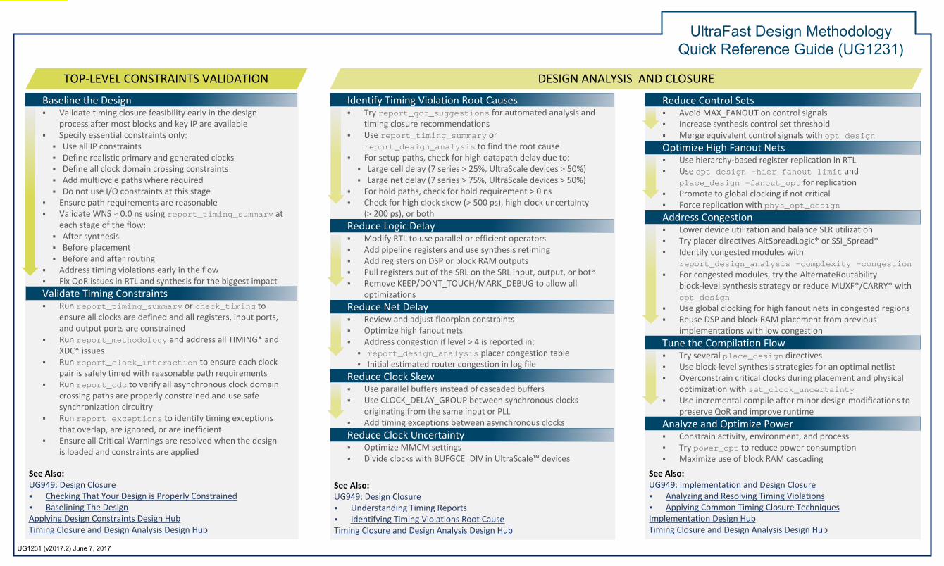
See Also: UG949: Board and Device Planning PCB Design Checklist Memory Interface IP Design Checklists Schematic Design Checklists See Also: UG949: Board and Device Planning Power Estimation and Optimization Design Hub I/O and Clock Planning Design Hub The UltraFast™ Design Methodology is a set of best practices recommended by Xilinx to maximize productivity and reduce design iterations of complex systems, including embedded processor subsystems, analog and digital processing, highspeed connectivity, and network processing. See the UltraFast Design Methodology Guide for the Vivado Design Suite (UG949) for more information. The UltraFast Design Methodology Checklist (XTP301) includes common questions that highlight typical areas where design decisions have downstream consequences and draws attention to potential problems that are often unknown or ignored. It provides easy access to related collateral. The checklist is available within the Xilinx Documentation Navigator tool (DocNav). This quick reference guide highlights key design methodology steps to achieve quicker system integration and design implementation and to derive the greatest value from Xilinx® devices and tools. Pointers to related collateral are also provided. The main design tasks covered in this guide include: Board and Device Planning Design Entry and Implementation TopLevel Design Validation Design Analysis Design Closure Refer to the UltraFast Design Methodology – SystemLevel Design Flow available within the Xilinx Documentation Navigator tool (DocNav) for pointers to all design hubs and specific collateral. UltraFast Design Methodology Quick Reference Guide (UG1231) INTRODUCTION BOARD AND DEVICE PLANNING DESIGN ENTRY AND IMPLEMENTATION See Also: UG949: Design Creation and Implementation Designing with IP Design Hub Using IP Integrator Design Hub Logic Synthesis Design Hub Applying Design Constraints Design Hub Implementation Design Hub PCB Designer FPGA Designer Analyze Device for Pinout Examine transceiver and bonded I/O locations Examine SSI technology I/O planning Validate part orientation and key interfaces Define I/O Pinouts for Key Interfaces Create I/O planning projects Define and validate memory controllers, GTs, and PCIe® technology locations Establish a clocking skeleton Minimize floorplan distance between connected IP Define Final Pinout Merge interface projects into a final I/O project Validate DRCs and SSN analysis Implement design to check clocking and I/O rules Use the final I/O project for production test Estimate Power Determine power budget and thermal margin using Xilinx Power Estimator (XPE) Apply toggle rates using knowledge of prior designs Define a Good Design Hierarchy Define relevant hierarchies to help global placement and floorplanning Insert I/O and clock components near the top level Add registers at main hierarchical boundaries Generate IP and review target device utilization Build and Validate RTL Submodules Ensure design adheres to RTL coding guidelines Add sufficient registers around DSP and memories Use control signals only when absolutely necessary Use synthesis attributes to control final logic mapping Create simple timing constraints to review estimated timing and address paths with too many logic levels Review synthesis log files, utilization report, and elaborated view to identify suboptimal mapping Run Methodology and RTL checks and review issues Implement the submodule in outofcontext (OOC) mode to validate implemented performance Review utilization and power against original budget Simulate the design to validate functionality Assemble and Validate TopLevel Design Synthesize the toplevel RTL design and resolve all connectivity issues Review toplevel utilization and clocking guidelines Create and validate toplevel constraints Iterate the RTL and constraints to fix Methodology and DRC issues and meet timing Proceed to implementation Logic Designer UG1231 (v2017.2) June 7, 2017 Examine Key Interfaces Validate part orientation and key interfaces Examine the PCB Layout Perform the Memory Interface and Transceiver Checklists Follow PCB layout recommendations Ensure final FPGA pinout is signed off by FPGA designer Review the Schematic Complete PCB Checklist review Check PDS, configuration, and power supplies Validate I/O state before, during, and after configuration Manufacture and Test Verify the configuration sequence, power supplies, and I/O performance with the test I/O project
Transcript

See Also:UG949: Board and Device PlanningPCB Design ChecklistMemory Interface IP Design ChecklistsSchematic Design Checklists

See Also:UG949: Board and Device PlanningPower Estimation and Optimization Design HubI/O and Clock Planning Design Hub

The UltraFast™ Design Methodology is a set of best practices recommended by Xilinx to maximize productivity and reduce design iterations of complex systems, including embedded processor subsystems, analog and digital processing, high‐speed connectivity, and network processing. See the UltraFast Design Methodology Guide for the Vivado Design Suite (UG949) for more information.

The UltraFast Design Methodology Checklist (XTP301) includes common questions that highlight typical areas where design decisions have downstream consequences and draws attention to potential problems that are often unknown or ignored. It provides easy access to related collateral. The checklist is available within the Xilinx Documentation Navigator tool (DocNav).

This quick reference guide highlights key design methodology steps to achieve quicker system integration and design implementation and to derive the greatest value from Xilinx® devices and tools. Pointers to related collateral are also provided. The main design tasks covered in this guide include: Board and Device Planning Design Entry and Implementation Top‐Level Design Validation Design Analysis  Design Closure

Refer to the UltraFast Design Methodology – System‐Level Design Flow available within the Xilinx Documentation Navigator tool (DocNav) for pointers to all design hubs and specific collateral.

UltraFast Design Methodology Quick Reference Guide (UG1231)

INTRODUCTION BOARD AND DEVICE PLANNING DESIGN ENTRY AND IMPLEMENTATION

See Also:UG949: Design Creation and ImplementationDesigning with IP Design HubUsing IP Integrator Design HubLogic Synthesis Design HubApplying Design Constraints Design HubImplementation Design Hub

PCB Designer FPGA DesignerAnalyze Device for Pinout Examine transceiver and 

bonded I/O locations Examine SSI technology I/O 

planning Validate part orientation 

and key interfacesDefine I/O Pinouts for Key Interfaces Create I/O planning projects Define and validate memory 

controllers, GTs, and PCIe® technology locations

Establish a clocking skeleton Minimize floorplan distance 

between connected IPDefine Final Pinout Merge interface projects 

into a final I/O project Validate DRCs and SSN 

analysis Implement design to check 

clocking and I/O rules Use the final I/O project for 

production testEstimate Power Determine power budget 

and thermal margin using Xilinx Power Estimator (XPE)

Apply toggle rates using knowledge of prior designs

Define a Good Design Hierarchy Define relevant hierarchies to help global placement and 

floorplanning Insert I/O and clock components near the top level Add registers at main hierarchical boundaries Generate IP and review target device utilizationBuild and Validate RTL Submodules Ensure design adheres to RTL coding guidelines Add sufficient registers around DSP and memories Use control signals only when absolutely necessary Use synthesis attributes to control final logic mapping Create simple timing constraints to review estimated 

timing and address paths with too many logic levels Review synthesis log files, utilization report, and 

elaborated view to identify sub‐optimal mapping Run Methodology and RTL checks and review issues Implement the submodule in out‐of‐context (OOC) mode 

to validate implemented performance Review utilization and power against original budget Simulate the design to validate functionalityAssemble and Validate Top‐Level Design Synthesize the top‐level RTL design and resolve all 

connectivity issues Review top‐level utilization and clocking guidelines Create and validate top‐level constraints Iterate the RTL and constraints to fix Methodology and 

DRC issues and meet timing Proceed to implementation

Logic Designer

UG1231 (v2017.2) June 7, 2017

Examine Key Interfaces Validate part orientation 

and key interfacesExamine the PCB Layout Perform the Memory 

Interface and Transceiver Checklists

Follow PCB layout recommendations

Ensure final FPGA pinout is signed off by FPGA designer

Review the Schematic Complete PCB Checklist 

review Check PDS, configuration, 

and power supplies Validate I/O state before, 

during, and after configuration

Manufacture and Test Verify the configuration 

sequence, power supplies, and I/O performance with the test I/O project

UltraFast Design Methodology Quick Reference Guide (UG1231)

TOP‐LEVEL CONSTRAINTS VALIDATION DESIGN ANALYSIS  AND CLOSURE

See Also:UG949: Implementation and Design Closure Analyzing and Resolving Timing Violations Applying Common Timing Closure TechniquesImplementation Design HubTiming Closure and Design Analysis Design Hub

See Also:UG949: Design Closure  Understanding Timing Reports Identifying Timing Violations Root CauseTiming Closure and Design Analysis Design Hub

Identify Timing Violation Root Causes Try report_qor_suggestions for automated analysis and 

timing closure recommendations Use report_timing_summary or 

report_design_analysis to find the root cause For setup paths, check for high datapath delay due to:Large cell delay (7 series > 25%, UltraScale devices > 50%)Large net delay (7 series > 75%, UltraScale devices > 50%)

For hold paths, check for hold requirement > 0 ns Check for high clock skew (> 500 ps), high clock uncertainty 

(> 200 ps), or bothReduce Logic Delay Modify RTL to use parallel or efficient operators Add pipeline registers and use synthesis retiming Add registers on DSP or block RAM outputs Pull registers out of the SRL on the SRL input, output, or both Remove KEEP/DONT_TOUCH/MARK_DEBUG to allow all 

optimizationsReduce Net Delay Review and adjust floorplan constraints Optimize high fanout nets Address congestion if level > 4 is reported in:report_design_analysis placer congestion tableInitial estimated router congestion in log file

Reduce Clock Skew Use parallel buffers instead of cascaded buffers Use CLOCK_DELAY_GROUP between synchronous clocks 

originating from the same input or PLL Add timing exceptions between asynchronous clocksReduce Clock Uncertainty Optimize MMCM settings  Divide clocks with BUFGCE_DIV in UltraScale™ devices

See Also:UG949: Design Closure Checking That Your Design is Properly Constrained Baselining The DesignApplying Design Constraints Design HubTiming Closure and Design Analysis Design Hub

Baseline the Design Validate timing closure feasibility early in the design 

process after most blocks and key IP are available Specify essential constraints only: Use all IP constraintsDefine realistic primary and generated clocksDefine all clock domain crossing constraintsAdd multicycle paths where requiredDo not use I/O constraints at this stage

Ensure path requirements are reasonable Validate WNS ≈ 0.0 ns using report_timing_summary at 

each stage of the flow:After synthesisBefore placementBefore and after routing

Address timing violations early in the flow Fix QoR issues in RTL and synthesis for the biggest impactValidate Timing Constraints Run report_timing_summary or check_timing to 

ensure all clocks are defined and all registers, input ports, and output ports are constrained

Run report_methodology and address all TIMING* and XDC* issues

Run report_clock_interaction to ensure each clock pair is safely timed with reasonable path requirements

Run report_cdc to verify all asynchronous clock domain crossing paths are properly constrained and use safe synchronization circuitry

Run report_exceptions to identify timing exceptions that overlap, are ignored, or are inefficient

Ensure all Critical Warnings are resolved when the design is loaded and constraints are applied

UG1231 (v2017.2) June 7, 2017

Reduce Control Sets Avoid MAX_FANOUT on control signals Increase synthesis control set threshold Merge equivalent control signals with opt_designOptimize High Fanout Nets Use hierarchy‐based register replication in RTL Use opt_design -hier_fanout_limit and 

place_design -fanout_opt for replication Promote to global clocking if not critical Force replication with phys_opt_designAddress Congestion Lower device utilization and balance SLR utilization Try placer directives AltSpreadLogic* or SSI_Spread* Identify congested modules with 

report_design_analysis -complexity -congestion For congested modules, try the AlternateRoutability 

block‐level synthesis strategy or reduce MUXF*/CARRY* with  opt_design

Use global clocking for high fanout nets in congested regions Reuse DSP and block RAM placement from previous 

implementations with low congestionTune the Compilation Flow Try several place_design directives Use block‐level synthesis strategies for an optimal netlist Overconstrain critical clocks during placement and physical 

optimization with set_clock_uncertainty Use incremental compile after minor design modifications to 

preserve QoR and improve runtimeAnalyze and Optimize Power Constrain activity, environment, and process Try power_opt to reduce power consumption Maximize use of block RAM cascading


Recommended