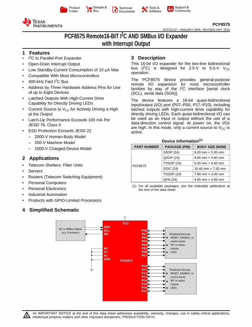
PCF8575 I2C or SMBus Master (e.g. Processor) Peripheral Devices ● RESET, ENABLE, or control inputs ● INT or status outputs ● LEDs SDA SCL INT A0 A1 A2 GND VCC P00 P01 P02 P03 P04 P05 P06 P07 Peripheral Devices RESET, ENABLE, or control inputs INT or status outputs LEDs P10 P11 P12 P13 P14 P15 P16 P17 ● ● ● Product Folder Sample & Buy Technical Documents Tools & Software Support & Community PCF8575 SCPS121F – JANUARY 2005 – REVISED MAY 2015 PCF8575 Remote16-BIT I 2 C AND SMBus I/O Expander with Interrupt Output 1 1 Features • I 2 C to Parallel-Port Expander 3 Description This 16-bit I/O expander for the two-line bidirectional • Open-Drain Interrupt Output bus (I 2 C) is designed for 2.5-V to 5.5-V V CC • Low Standby-Current Consumption of 10 μA Max operation. • Compatible With Most Microcontrollers The PCF8575 device provides general-purpose • 400-kHz Fast I 2 C Bus remote I/O expansion for most microcontroller • Address by Three Hardware Address Pins for Use families by way of the I 2 C interface [serial clock of up to Eight Devices (SCL), serial data (SDA)]. • Latched Outputs With High-Current Drive The device features a 16-bit quasi-bidirectional Capability for Directly Driving LEDs input/output (I/O) port (P07–P00, P17–P10), including • Current Source to V CC for Actively Driving a High latched outputs with high-current drive capability for directly driving LEDs. Each quasi-bidirectional I/O can at the Output be used as an input or output without the use of a • Latch-Up Performance Exceeds 100 mA Per data-direction control signal. At power on, the I/Os JESD 78, Class II are high. In this mode, only a current source to V CC is • ESD Protection Exceeds JESD 22 active. – 2000-V Human-Body Model Device Information (1) – 200-V Machine Model PART NUMBER PACKAGE (PIN) BODY SIZE (NOM) – 1000-V Charged-Device Model SSOP (24) 8.20 mm × 5.30 mm QSOP (24) 8.65 mm × 3.90 mm 2 Applications TVSOP (24) 5.00 mm × 4.50 mm • Telecom Shelters: Filter Units PCF8575 SOIC (24) 15.40 mm × 7.50 mm • Servers TSSOP (24) 7.80 mm × 4.40 mm • Routers (Telecom Switching Equipment) QFN (24) 4.00 mm × 4.00 mm • Personal Computers (1) For all available packages, see the orderable addendum at • Personal Electronics the end of the data sheet. • Industrial Automation • Products with GPIO-Limited Processors 4 Simplified Schematic 1 An IMPORTANT NOTICE at the end of this data sheet addresses availability, warranty, changes, use in safety-critical applications, intellectual property matters and other important disclaimers. PRODUCTION DATA.
Transcript
PCF8575
I2C or SMBus Master
(e.g. Processor)Peripheral Devices
● RESET, ENABLE, or
control inputs
● INT or status
outputs
● LEDs
SDA
SCL
INT
A0
A1
A2
GND
VCC
P00
P01
P02
P03
P04
P05
P06
P07
Peripheral Devices
RESET, ENABLE, or
control inputs
INT or status
outputs
LEDs
P10
P11
P12
P13
P14
P15
P16
P17
●
●
●
Product
Folder
Sample &Buy
Technical
Documents
Tools &
Software
Support &Community
PCF8575SCPS121F –JANUARY 2005–REVISED MAY 2015
PCF8575 Remote16-BIT I2C AND SMBus I/O Expanderwith Interrupt Output
1
1 Features• I2C to Parallel-Port Expander 3 Description
This 16-bit I/O expander for the two-line bidirectional• Open-Drain Interrupt Outputbus (I2C) is designed for 2.5-V to 5.5-V VCC• Low Standby-Current Consumption of 10 μA Maxoperation.
• Compatible With Most MicrocontrollersThe PCF8575 device provides general-purpose• 400-kHz Fast I2C Bus remote I/O expansion for most microcontroller
• Address by Three Hardware Address Pins for Use families by way of the I2C interface [serial clockof up to Eight Devices (SCL), serial data (SDA)].
• Latched Outputs With High-Current Drive The device features a 16-bit quasi-bidirectionalCapability for Directly Driving LEDs input/output (I/O) port (P07–P00, P17–P10), including
• Current Source to VCC for Actively Driving a High latched outputs with high-current drive capability fordirectly driving LEDs. Each quasi-bidirectional I/O canat the Outputbe used as an input or output without the use of a• Latch-Up Performance Exceeds 100 mA Perdata-direction control signal. At power on, the I/OsJESD 78, Class II are high. In this mode, only a current source to VCC is
• ESD Protection Exceeds JESD 22 active.– 2000-V Human-Body Model
Device Information(1)– 200-V Machine Model
PART NUMBER PACKAGE (PIN) BODY SIZE (NOM)– 1000-V Charged-Device ModelSSOP (24) 8.20 mm × 5.30 mmQSOP (24) 8.65 mm × 3.90 mm2 ApplicationsTVSOP (24) 5.00 mm × 4.50 mm• Telecom Shelters: Filter Units PCF8575SOIC (24) 15.40 mm × 7.50 mm• ServersTSSOP (24) 7.80 mm × 4.40 mm
• Routers (Telecom Switching Equipment)QFN (24) 4.00 mm × 4.00 mm
• Personal Computers(1) For all available packages, see the orderable addendum at
• Personal Electronics the end of the data sheet.• Industrial Automation• Products with GPIO-Limited Processors
4 Simplified Schematic
1
An IMPORTANT NOTICE at the end of this data sheet addresses availability, warranty, changes, use in safety-critical applications,intellectual property matters and other important disclaimers. PRODUCTION DATA.
14 Mechanical, Packaging, and Orderable9 Detailed Description ............................................ 12 Information ........................................................... 25
5 Revision History
Changes from Revision E (January 2015) to Revision F Page
• Fixed naming typo in pin out graphic. ................................................................................................................................... 3
Changes from Revision D (April 2007) to Revision E Page
• Added Applications, Device Information table, Pin Functions table, ESD Ratings table, Thermal Information table,Typical Characteristics, Feature Description section, Device Functional Modes, Application and Implementationsection, Power Supply Recommendations section, Layout section, Device and Documentation Support section, andMechanical, Packaging, and Orderable Information section. ................................................................................................. 1
• Deleted Ordering Information table. ....................................................................................................................................... 1
PCF8575SCPS121F –JANUARY 2005–REVISED MAY 2015 www.ti.com
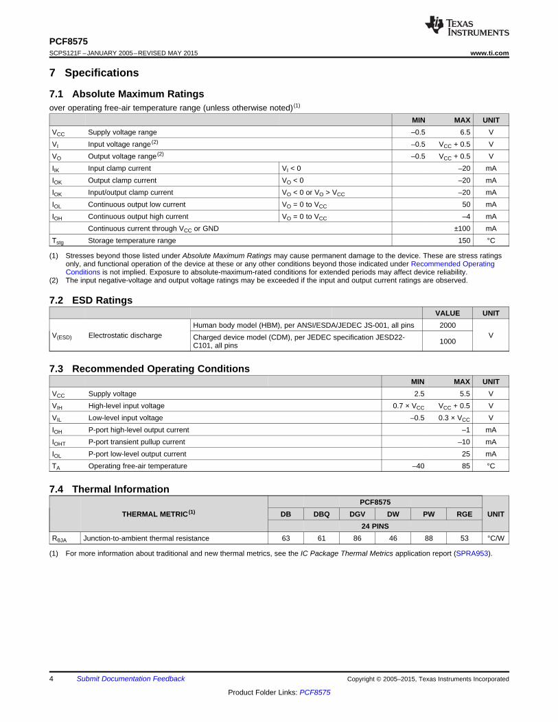
7 Specifications
7.1 Absolute Maximum Ratingsover operating free-air temperature range (unless otherwise noted) (1)
MIN MAX UNITVCC Supply voltage range –0.5 6.5 VVI Input voltage range (2) –0.5 VCC + 0.5 VVO Output voltage range (2) –0.5 VCC + 0.5 VIIK Input clamp current VI < 0 –20 mAIOK Output clamp current VO < 0 –20 mAIOK Input/output clamp current VO < 0 or VO > VCC –20 mAIOL Continuous output low current VO = 0 to VCC 50 mAIOH Continuous output high current VO = 0 to VCC –4 mA
Continuous current through VCC or GND ±100 mATstg Storage temperature range 150 °C
(1) Stresses beyond those listed under Absolute Maximum Ratings may cause permanent damage to the device. These are stress ratingsonly, and functional operation of the device at these or any other conditions beyond those indicated under Recommended OperatingConditions is not implied. Exposure to absolute-maximum-rated conditions for extended periods may affect device reliability.
(2) The input negative-voltage and output voltage ratings may be exceeded if the input and output current ratings are observed.
7.2 ESD RatingsVALUE UNIT
Human body model (HBM), per ANSI/ESDA/JEDEC JS-001, all pins 2000V(ESD) Electrostatic discharge VCharged device model (CDM), per JEDEC specification JESD22- 1000C101, all pins
7.3 Recommended Operating ConditionsMIN MAX UNIT
VCC Supply voltage 2.5 5.5 VVIH High-level input voltage 0.7 × VCC VCC + 0.5 VVIL Low-level input voltage –0.5 0.3 × VCC VIOH P-port high-level output current –1 mAIOHT P-port transient pullup current –10 mAIOL P-port low-level output current 25 mATA Operating free-air temperature –40 85 °C
PCF8575www.ti.com SCPS121F –JANUARY 2005–REVISED MAY 2015
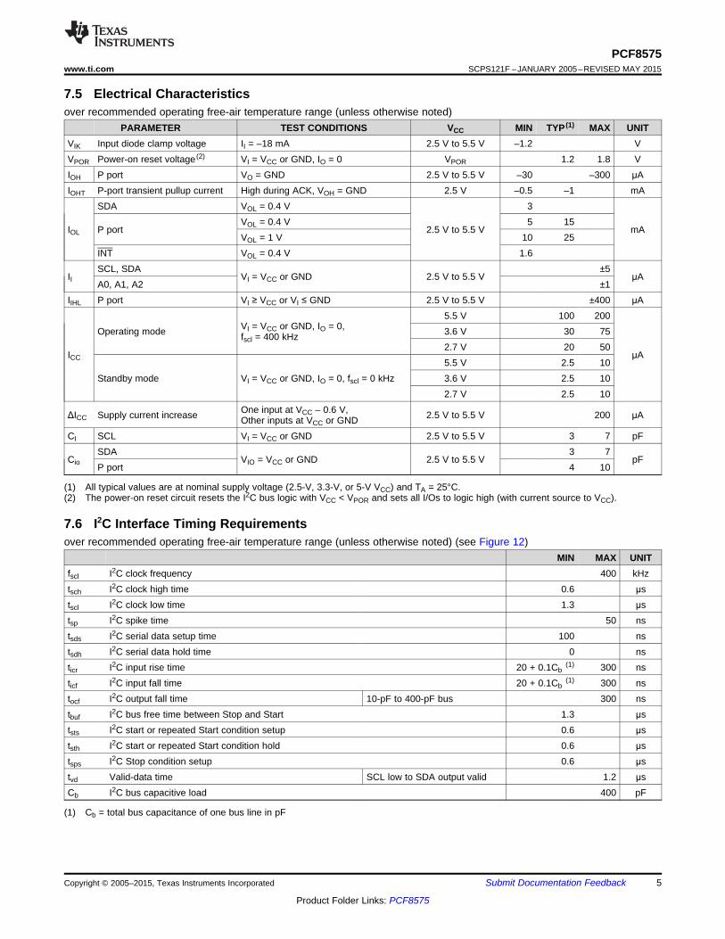
7.5 Electrical Characteristicsover recommended operating free-air temperature range (unless otherwise noted)
PARAMETER TEST CONDITIONS VCC MIN TYP (1) MAX UNITVIK Input diode clamp voltage II = –18 mA 2.5 V to 5.5 V –1.2 VVPOR Power-on reset voltage (2) VI = VCC or GND, IO = 0 VPOR 1.2 1.8 VIOH P port VO = GND 2.5 V to 5.5 V –30 –300 μAIOHT P-port transient pullup current High during ACK, VOH = GND 2.5 V –0.5 –1 mA
SDA VOL = 0.4 V 3VOL = 0.4 V 5 15
IOL P port 2.5 V to 5.5 V mAVOL = 1 V 10 25
INT VOL = 0.4 V 1.6SCL, SDA ±5
II VI = VCC or GND 2.5 V to 5.5 V μAA0, A1, A2 ±1
IIHL P port VI ≥ VCC or VI ≤ GND 2.5 V to 5.5 V ±400 μA5.5 V 100 200
VI = VCC or GND, IO = 0,Operating mode 3.6 V 30 75fscl = 400 kHz2.7 V 20 50
ICC μA5.5 V 2.5 10
Standby mode VI = VCC or GND, IO = 0, fscl = 0 kHz 3.6 V 2.5 102.7 V 2.5 10
One input at VCC – 0.6 V,ΔICC Supply current increase 2.5 V to 5.5 V 200 μAOther inputs at VCC or GNDCI SCL VI = VCC or GND 2.5 V to 5.5 V 3 7 pF
SDA 3 7Cio VIO = VCC or GND 2.5 V to 5.5 V pF
P port 4 10
(1) All typical values are at nominal supply voltage (2.5-V, 3.3-V, or 5-V VCC) and TA = 25°C.(2) The power-on reset circuit resets the I2C bus logic with VCC < VPOR and sets all I/Os to logic high (with current source to VCC).
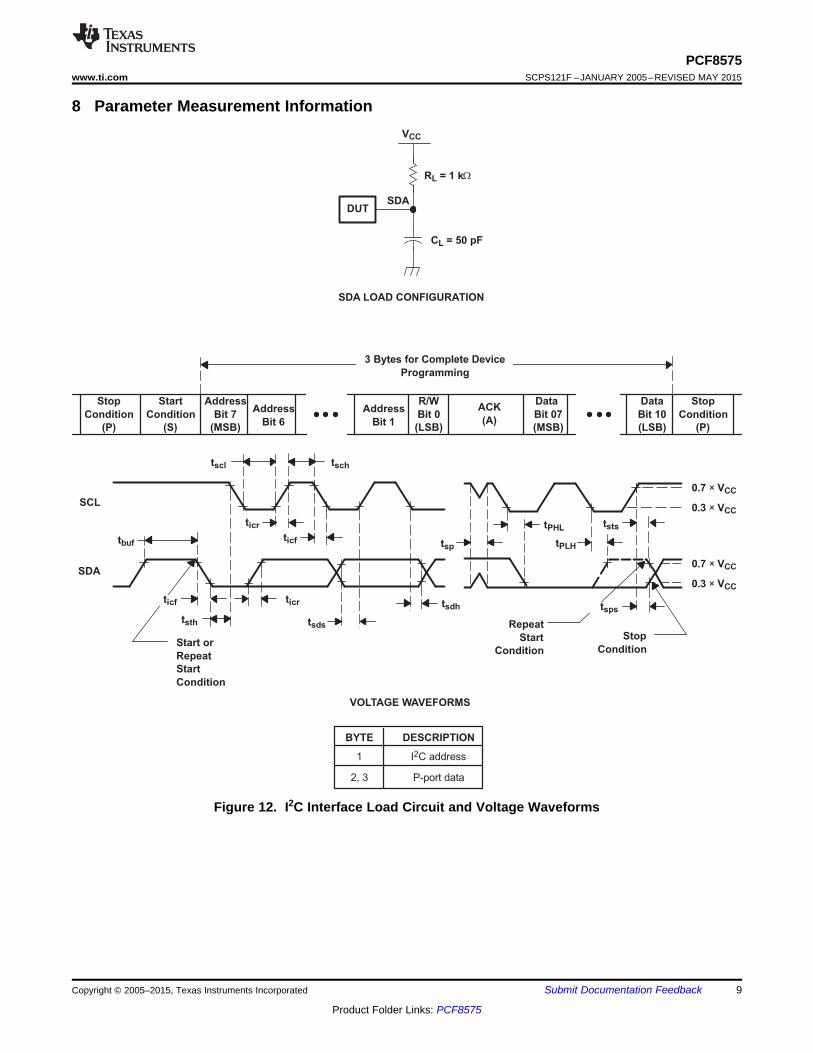
7.6 I2C Interface Timing Requirementsover recommended operating free-air temperature range (unless otherwise noted) (see Figure 12)
MIN MAX UNITfscl I2C clock frequency 400 kHztsch I2C clock high time 0.6 μstscl I2C clock low time 1.3 μstsp I2C spike time 50 nstsds I2C serial data setup time 100 nstsdh I2C serial data hold time 0 nsticr I2C input rise time 20 + 0.1Cb
(1) 300 nsticf I2C input fall time 20 + 0.1Cb
(1) 300 nstocf I2C output fall time 10-pF to 400-pF bus 300 nstbuf I2C bus free time between Stop and Start 1.3 μststs I2C start or repeated Start condition setup 0.6 μststh I2C start or repeated Start condition hold 0.6 μstsps I2C Stop condition setup 0.6 μstvd Valid-data time SCL low to SDA output valid 1.2 μsCb I2C bus capacitive load 400 pF
(1) Cb = total bus capacitance of one bus line in pF
PCF8575SCPS121F –JANUARY 2005–REVISED MAY 2015 www.ti.com
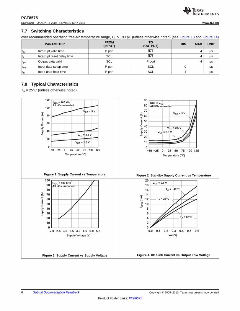
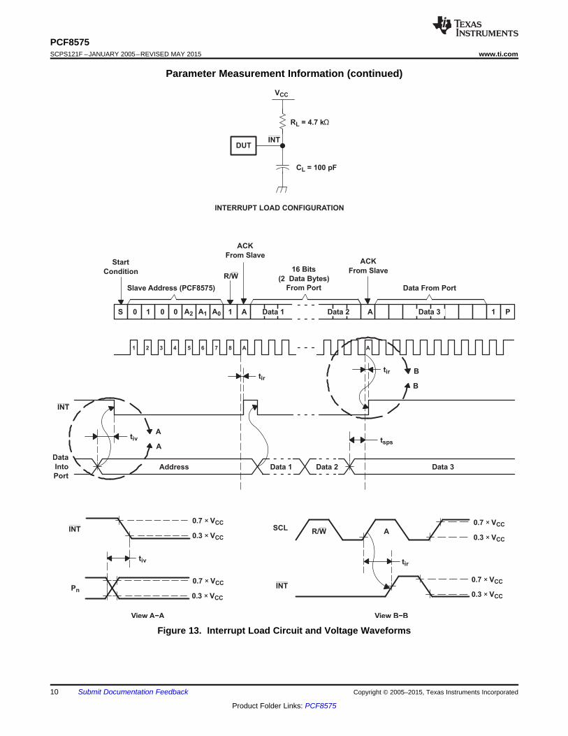
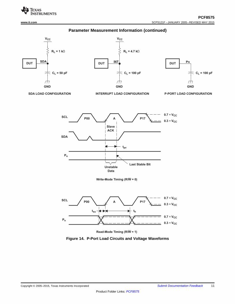
7.7 Switching Characteristicsover recommended operating free-air temperature range, CL ≤ 100 pF (unless otherwise noted) (see Figure 13 and Figure 14)
FROM TOPARAMETER MIN MAX UNIT(INPUT) (OUTPUT)tiv Interrupt valid time P port INT 4 μstir Interrupt reset delay time SCL INT 4 μstpv Output data valid SCL P port 4 μstsu Input data setup time P port SCL 0 μsth Input data hold time P port SCL 4 μs
PCF8575SCPS121F –JANUARY 2005–REVISED MAY 2015 www.ti.com
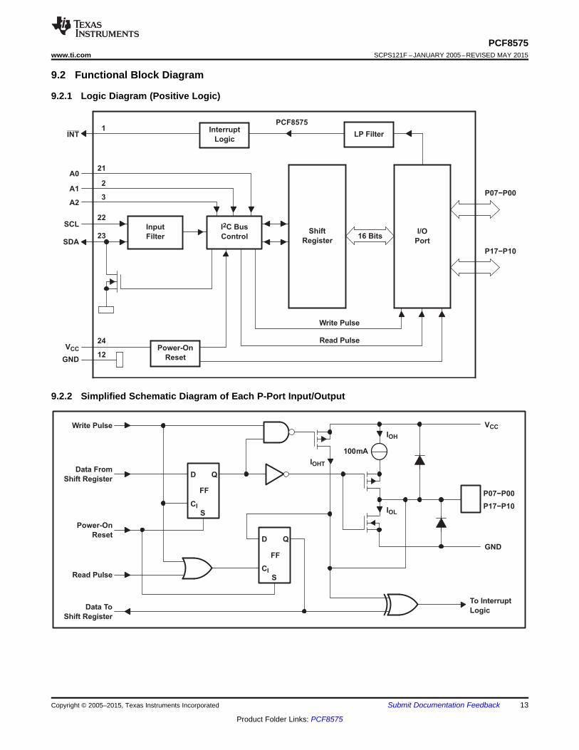
9 Detailed Description
9.1 OverviewThe PCF8575 provides general-purpose remote I/O expansion for most microcontroller families via the I2Cinterface serial clock (SCL) and serial data (SDA).
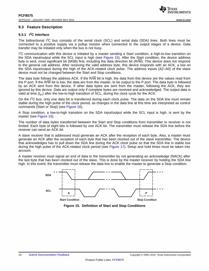
The device features a 16-bit quasi-bidirectional input/output (I/O) port (P07–P00, P17–P10), including latchedoutputs with high-current drive capability for directly driving LEDs. Each quasi-bidirectional I/O can be used as aninput or output without the use of a data-direction control signal. At power on, the I/Os are high. In this mode,only a current source (IOH) to VCC is active. An additional strong pullup to VCC (IOHT) allows fast-rising edges intoheavily loaded outputs. This device turns on when an output is written high and is switched off by the negativeedge of SCL. The I/Os should be high before being used as inputs. After power on, as all the I/Os are set high,all of them can be used as inputs. Any change in setting of the I/Os as either input or outputs can be done withthe write mode. If a high is applied externally to an I/O that has been written earlier to low, a large current (IOL)will flow to GND.
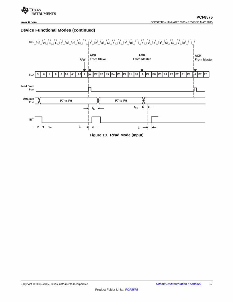
The PCF8575 provides an open-drain interrupt (INT) output, which can be connected to the interrupt input of amicrocontroller. An interrupt is generated by any rising or falling edge of the port inputs in the input mode. Aftertime, tiv, the signal INT is valid. Resetting and reactivating the interrupt circuit is achieved when data on the portis changed to the original setting, or data is read from or written to the port that generated the interrupt. Resettingoccurs in the read mode at the acknowledge (ACK) bit after the rising edge of the SCL signal or in the writemode at the ACK bit after the falling edge of the SCL signal. Interrupts that occur during the ACK clock pulse canbe lost (or be very short), due to the resetting of the interrupt during this pulse. Each change of the I/Os afterresetting is detected and is transmitted as INT. Reading from or writing to another device does not affect theinterrupt circuit. This device does not have internal configuration or status registers. Instead, read or write to thedevice I/Os directly after sending the device address (see Figure 18 and Figure 19).
By sending an interrupt signal on this line, the remote I/O can inform the microcontroller if there is incoming dataon its ports, without having to communicate via the I2C bus. Thus, the PCF8575 can remain a simple slavedevice.
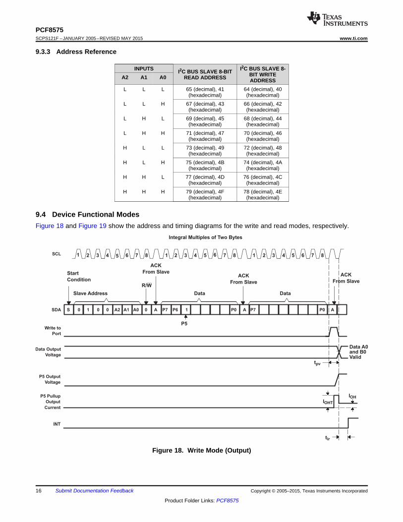
Every data transmission to or from the PCF8575 must consist of an even number of bytes. The first data byte inevery pair refers to port 0 (P07–P00), and the second data byte in every pair refers to port 1 (P17–P10). To writeto the ports (output mode), the master first addresses the slave device, setting the last bit of the byte containingthe slave address to logic 0. The PCF8575 acknowledges, and the master sends the first data byte for P07–P00.After the first data byte is acknowledged by the PCF8575, the second data byte (P17–P10) is sent by the master.Once again, the PCF8575 acknowledges the receipt of the data, after which this 16-bit data is presented on theport lines.
The number of data bytes that can be sent successively is not limited. After every two bytes, the previous data isoverwritten. When the PCF8575 receives the pairs of data bytes, the first byte is referred to as P07–P00 and thesecond byte as P17–P10. The third byte is referred to as P07–P00, the fourth byte as P17–P10, and so on.
Before reading from the PCF8575, all ports desired as input should be set to logic 1. To read from the ports(input mode), the master first addresses the slave device, setting the last bit of the byte containing the slaveaddress to logic 1. The data bytes that follow on the SDA are the values on the ports. If the data on the input portchanges faster than the master can read, this data may be lost.
When power is applied to VCC, an internal power-on reset holds the PCF8575 in a reset state until VCC hasreached VPOR. At that time, the reset condition is released, and the device I2C-bus state machine initializes thebus to its default state.
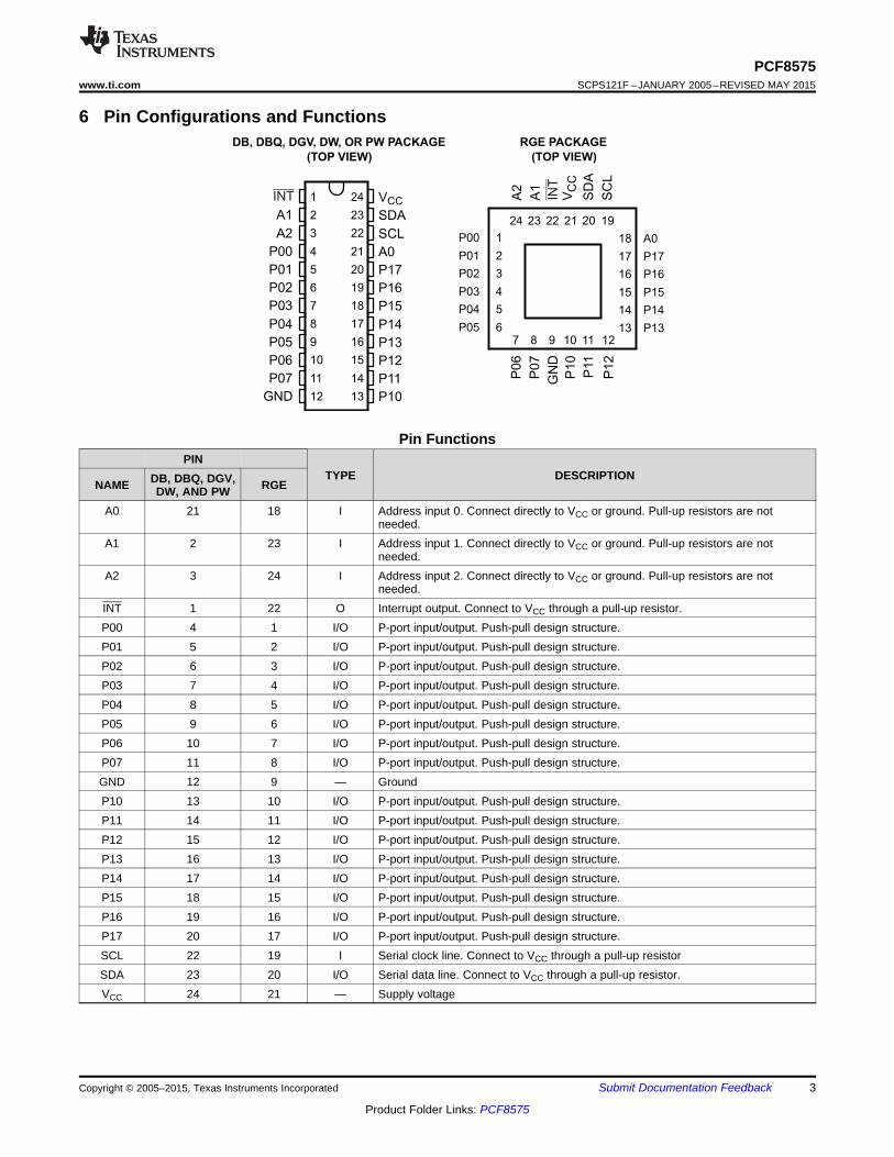
The hardware pins (A0, A1, and A2) are used to program and vary the fixed I2C address and allow up to eightdevices to share the same I2C bus or SMBus. The fixed I2C address of the PCF8575 is the same as thePCF8575C, PCF8574, PCA9535, and PCA9555, allowing up to eight of these devices, in any combination, toshare the same I2C bus or SMBus.
PCF8575SCPS121F –JANUARY 2005–REVISED MAY 2015 www.ti.com
9.3 Feature Description
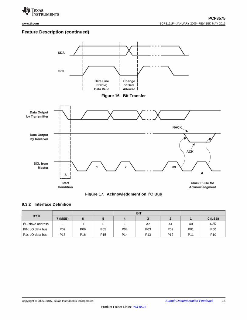
9.3.1 I2C InterfaceThe bidirectional I2C bus consists of the serial clock (SCL) and serial data (SDA) lines. Both lines must beconnected to a positive supply via a pullup resistor when connected to the output stages of a device. Datatransfer may be initiated only when the bus is not busy.
I2C communication with this device is initiated by a master sending a Start condition, a high-to-low transition onthe SDA input/output while the SCL input is high (see Figure 15). After the Start condition, the device addressbyte is sent, most significant bit (MSB) first, including the data direction bit (R/W). This device does not respondto the general call address. After receiving the valid address byte, this device responds with an ACK, a low onthe SDA input/output during the high of the ACK-related clock pulse. The address inputs (A2–A0) of the slavedevice must not be changed between the Start and Stop conditions.
The data byte follows the address ACK. If the R/W bit is high, the data from this device are the values read fromthe P port. If the R/W bit is low, the data are from the master, to be output to the P port. The data byte is followedby an ACK sent from this device. If other data bytes are sent from the master, following the ACK, they areignored by this device. Data are output only if complete bytes are received and acknowledged. The output data isvalid at time (tpv) after the low-to-high transition of SCL, during the clock cycle for the ACK.
On the I2C bus, only one data bit is transferred during each clock pulse. The data on the SDA line must remainstable during the high pulse of the clock period, as changes in the data line at this time are interpreted as controlcommands (Start or Stop) (see Figure 16).
A Stop condition, a low-to-high transition on the SDA input/output while the SCL input is high, is sent by themaster (see Figure 15).
The number of data bytes transferred between the Start and Stop conditions from transmitter to receiver is notlimited. Each byte of eight bits is followed by one ACK bit. The transmitter must release the SDA line before thereceiver can send an ACK bit.
A slave receiver that is addressed must generate an ACK after the reception of each byte. Also, a master mustgenerate an ACK after the reception of each byte that has been clocked out of the slave transmitter. The devicethat acknowledges has to pull down the SDA line during the ACK clock pulse so that the SDA line is stable lowduring the high pulse of the ACK-related clock period (see Figure 17). Setup and hold times must be taken intoaccount.
A master receiver must signal an end of data to the transmitter by not generating an acknowledge (NACK) afterthe last byte that has been clocked out of the slave. This is done by the master receiver by holding the SDA linehigh. In this event, the transmitter must release the data line to enable the master to generate a Stop condition.
Figure 15. Definition of Start and Stop Conditions
PCF8575SCPS121F –JANUARY 2005–REVISED MAY 2015 www.ti.com
10 Application and Implementation
NOTEInformation in the following applications sections is not part of the TI componentspecification, and TI does not warrant its accuracy or completeness. TI’s customers areresponsible for determining suitability of components for their purposes. Customers shouldvalidate and test their design implementation to confirm system functionality.
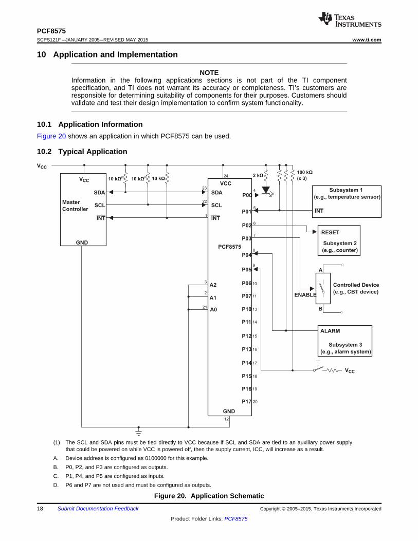
10.1 Application InformationFigure 20 shows an application in which PCF8575 can be used.
10.2 Typical Application
(1) The SCL and SDA pins must be tied directly to VCC because if SCL and SDA are tied to an auxiliary power supplythat could be powered on while VCC is powered off, then the supply current, ICC, will increase as a result.
A. Device address is configured as 0100000 for this example.B. P0, P2, and P3 are configured as outputs.C. P1, P4, and P5 are configured as inputs.D. P6 and P7 are not used and must be configured as outputs.
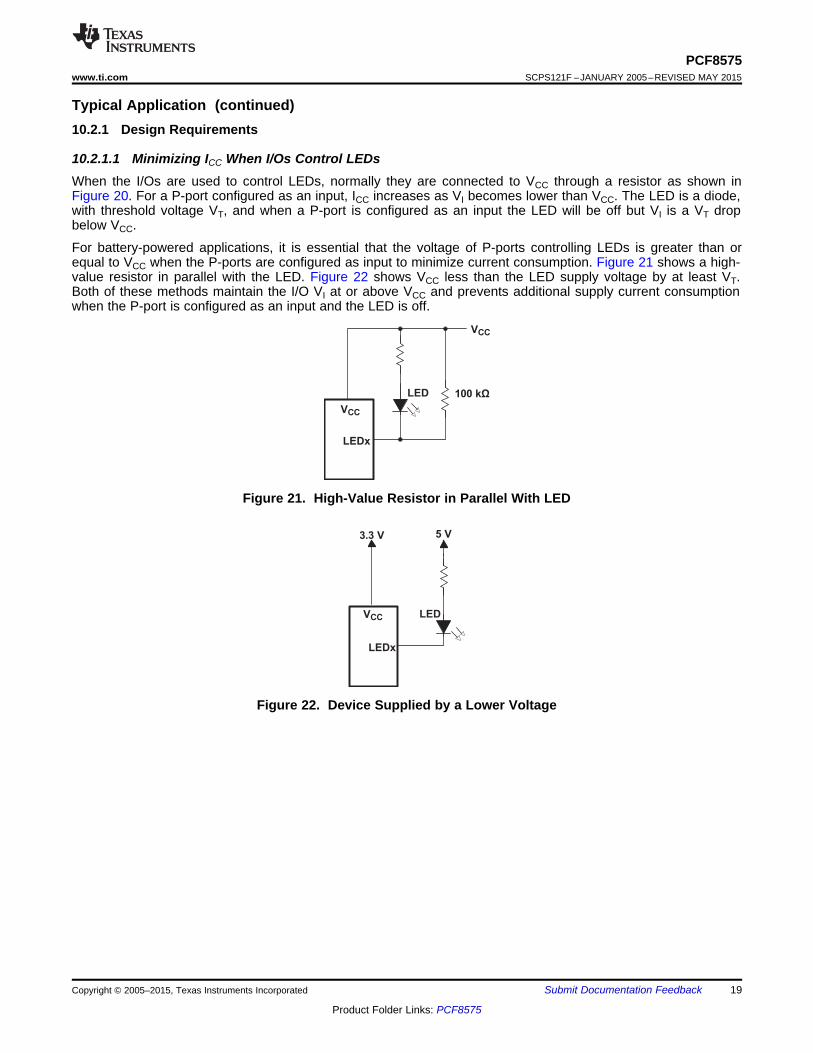
10.2.1.1 Minimizing ICC When I/Os Control LEDsWhen the I/Os are used to control LEDs, normally they are connected to VCC through a resistor as shown inFigure 20. For a P-port configured as an input, ICC increases as VI becomes lower than VCC. The LED is a diode,with threshold voltage VT, and when a P-port is configured as an input the LED will be off but VI is a VT dropbelow VCC.
For battery-powered applications, it is essential that the voltage of P-ports controlling LEDs is greater than orequal to VCC when the P-ports are configured as input to minimize current consumption. Figure 21 shows a high-value resistor in parallel with the LED. Figure 22 shows VCC less than the LED supply voltage by at least VT.Both of these methods maintain the I/O VI at or above VCC and prevents additional supply current consumptionwhen the P-port is configured as an input and the LED is off.
Figure 21. High-Value Resistor in Parallel With LED
PCF8575SCPS121F –JANUARY 2005–REVISED MAY 2015 www.ti.com
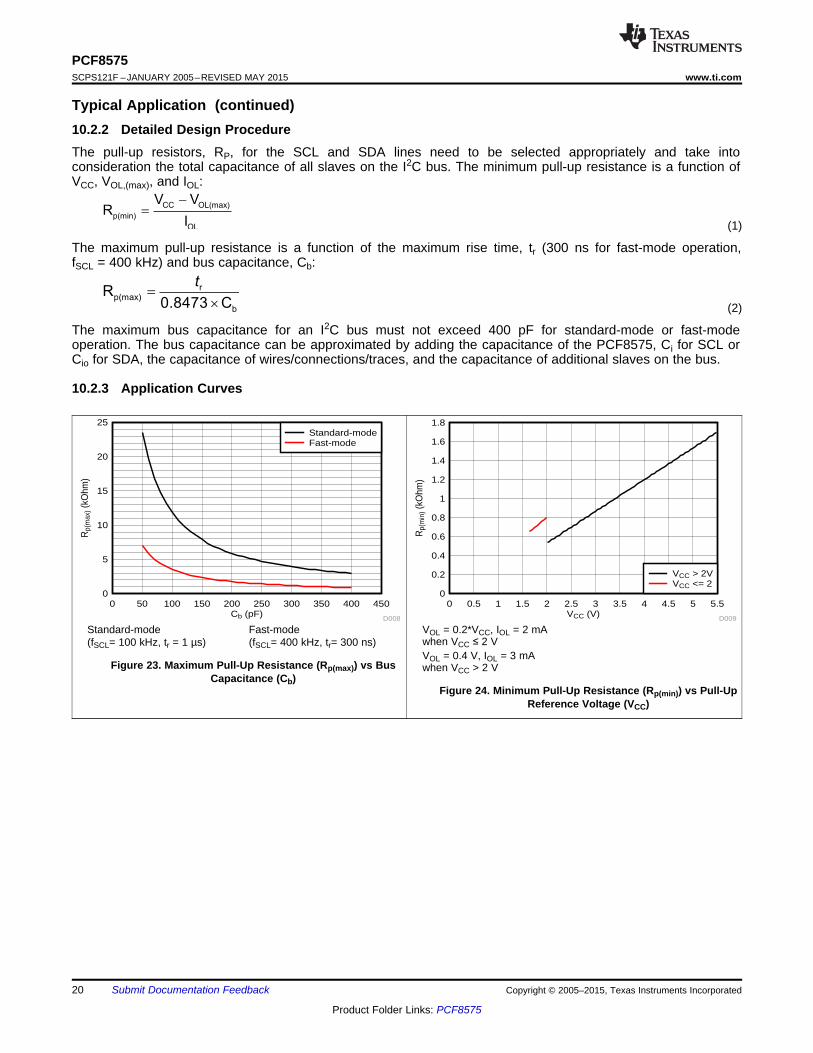
Typical Application (continued)10.2.2 Detailed Design ProcedureThe pull-up resistors, RP, for the SCL and SDA lines need to be selected appropriately and take intoconsideration the total capacitance of all slaves on the I2C bus. The minimum pull-up resistance is a function ofVCC, VOL,(max), and IOL:
(1)
The maximum pull-up resistance is a function of the maximum rise time, tr (300 ns for fast-mode operation,fSCL = 400 kHz) and bus capacitance, Cb:
(2)
The maximum bus capacitance for an I2C bus must not exceed 400 pF for standard-mode or fast-modeoperation. The bus capacitance can be approximated by adding the capacitance of the PCF8575, Ci for SCL orCio for SDA, the capacitance of wires/connections/traces, and the capacitance of additional slaves on the bus.
PCF8575www.ti.com SCPS121F –JANUARY 2005–REVISED MAY 2015
11 Power Supply Recommendations
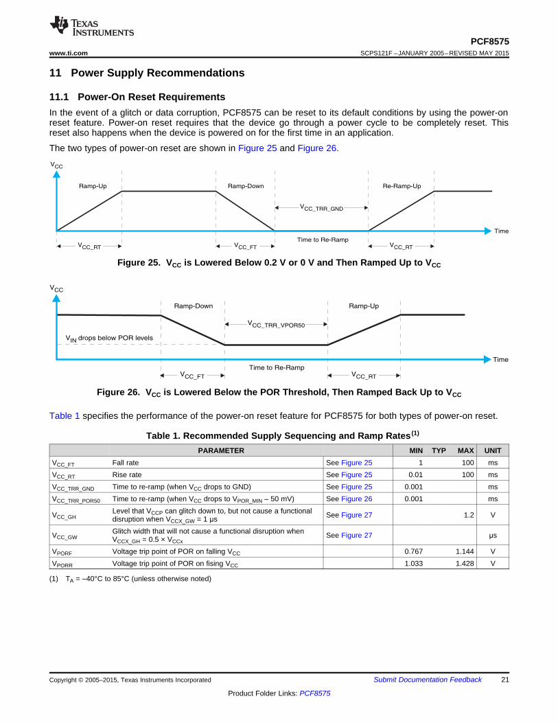
11.1 Power-On Reset RequirementsIn the event of a glitch or data corruption, PCF8575 can be reset to its default conditions by using the power-onreset feature. Power-on reset requires that the device go through a power cycle to be completely reset. Thisreset also happens when the device is powered on for the first time in an application.
The two types of power-on reset are shown in Figure 25 and Figure 26.
Figure 25. VCC is Lowered Below 0.2 V or 0 V and Then Ramped Up to VCC
Figure 26. VCC is Lowered Below the POR Threshold, Then Ramped Back Up to VCC
Table 1 specifies the performance of the power-on reset feature for PCF8575 for both types of power-on reset.
Table 1. Recommended Supply Sequencing and Ramp Rates (1)
PARAMETER MIN TYP MAX UNITVCC_FT Fall rate See Figure 25 1 100 msVCC_RT Rise rate See Figure 25 0.01 100 msVCC_TRR_GND Time to re-ramp (when VCC drops to GND) See Figure 25 0.001 msVCC_TRR_POR50 Time to re-ramp (when VCC drops to VPOR_MIN – 50 mV) See Figure 26 0.001 ms
Level that VCCP can glitch down to, but not cause a functionalVCC_GH See Figure 27 1.2 Vdisruption when VCCX_GW = 1 μsGlitch width that will not cause a functional disruption whenVCC_GW See Figure 27 μsVCCX_GH = 0.5 × VCCx
VPORF Voltage trip point of POR on falling VCC 0.767 1.144 VVPORR Voltage trip point of POR on fising VCC 1.033 1.428 V
PCF8575SCPS121F –JANUARY 2005–REVISED MAY 2015 www.ti.com
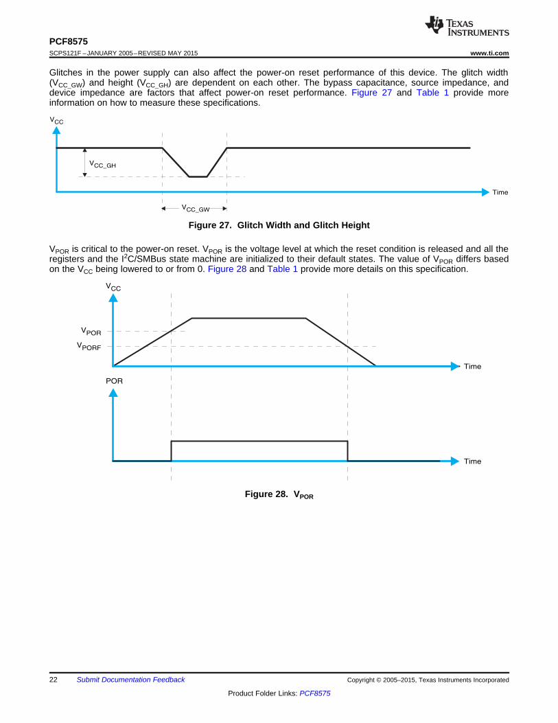
Glitches in the power supply can also affect the power-on reset performance of this device. The glitch width(VCC_GW) and height (VCC_GH) are dependent on each other. The bypass capacitance, source impedance, anddevice impedance are factors that affect power-on reset performance. Figure 27 and Table 1 provide moreinformation on how to measure these specifications.
Figure 27. Glitch Width and Glitch Height
VPOR is critical to the power-on reset. VPOR is the voltage level at which the reset condition is released and all theregisters and the I2C/SMBus state machine are initialized to their default states. The value of VPOR differs basedon the VCC being lowered to or from 0. Figure 28 and Table 1 provide more details on this specification.
PCF8575www.ti.com SCPS121F –JANUARY 2005–REVISED MAY 2015
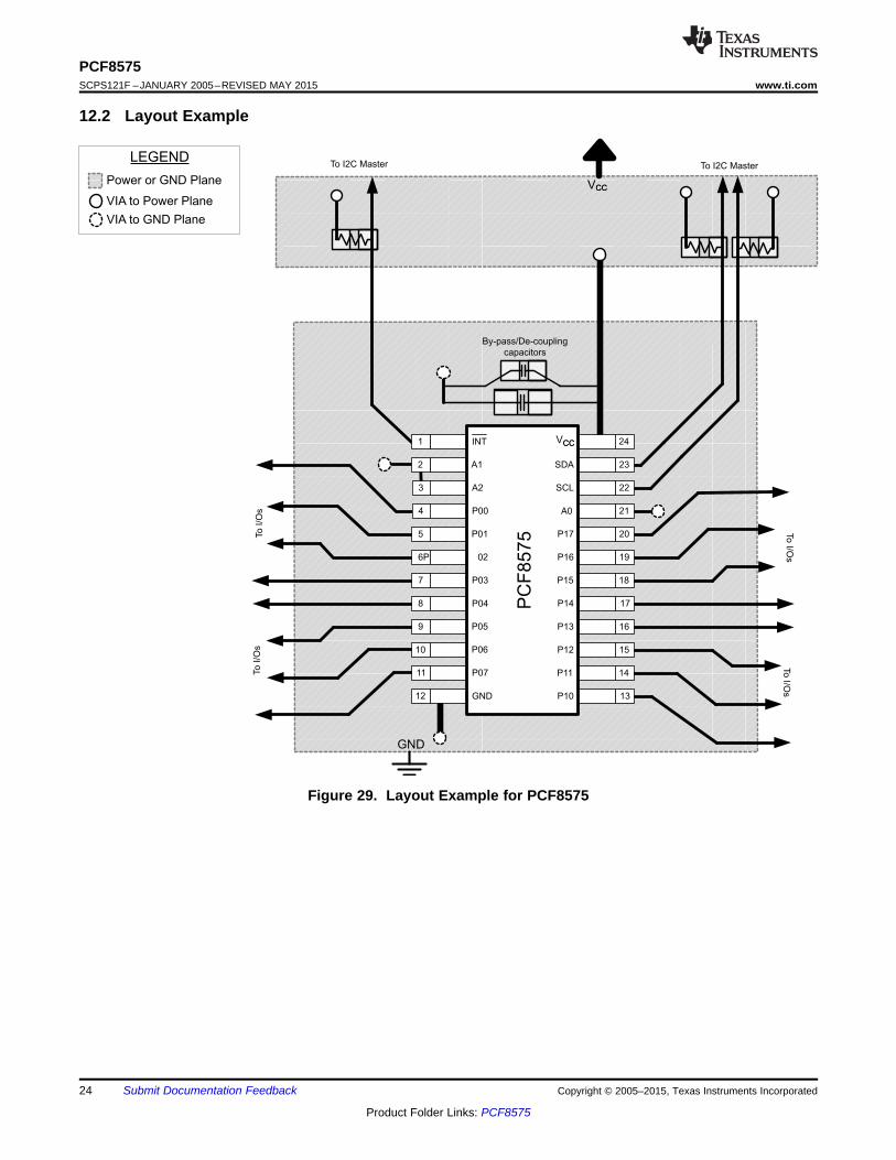
12 Layout
12.1 Layout GuidelinesFor printed circuit board (PCB) layout of the PCF8575 device, common PCB layout practices should be followedbut additional concerns related to high-speed data transfer such as matched impedances and differential pairsare not a concern for I2C signal speeds.
In all PCB layouts, it is a best practice to avoid right angles in signal traces, to fan out signal traces away fromeach other upon leaving the vicinity of an integrated circuit (IC), and to use thicker trace widths to carry higheramounts of current that commonly pass through power and ground traces. By-pass and de-coupling capacitorsare commonly used to control the voltage on the VCC pin, using a larger capacitor to provide additional power inthe event of a short power supply glitch and a smaller capacitor to filter out high-frequency ripple. Thesecapacitors should be placed as close to the PCF8575 as possible. These best practices are shown in Figure 29.
For the layout example provided in Figure 29, it would be possible to fabricate a PCB with only 2 layers by usingthe top layer for signal routing and the bottom layer as a split plane for power (VCC) and ground (GND). However,a 4 layer board is preferable for boards with higher density signal routing. On a 4 layer PCB, it is common toroute signals on the top and bottom layer, dedicate one internal layer to a ground plane, and dedicate the otherinternal layer to a power plane. In a board layout using planes or split planes for power and ground, vias areplaced directly next to the surface mount component pad which needs to attach to VCC or GND and the via isconnected electrically to the internal layer or the other side of the board. Vias are also used when a signal traceneeds to be routed to the opposite side of the board, but this technique is not demonstrated in Figure 29.
PCF8575www.ti.com SCPS121F –JANUARY 2005–REVISED MAY 2015
13 Device and Documentation Support
13.1 TrademarksAll trademarks are the property of their respective owners.
13.2 Electrostatic Discharge CautionThese devices have limited built-in ESD protection. The leads should be shorted together or the device placed in conductive foamduring storage or handling to prevent electrostatic damage to the MOS gates.
13.3 GlossarySLYZ022 — TI Glossary.
This glossary lists and explains terms, acronyms and definitions.
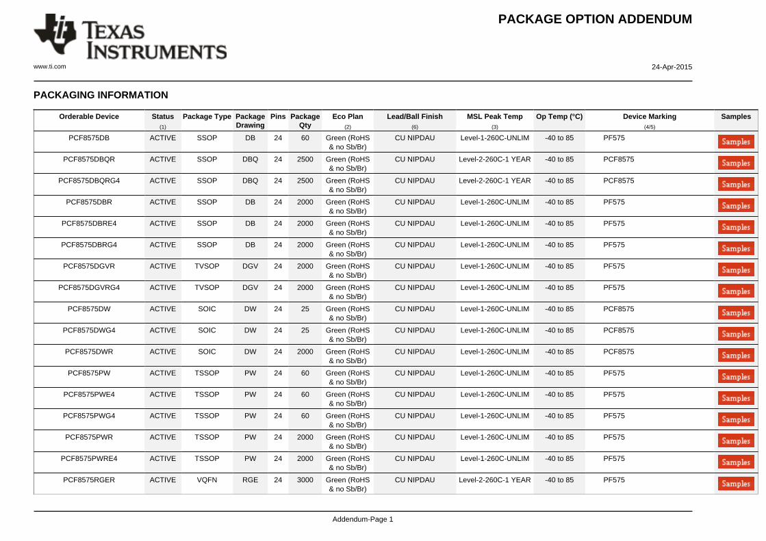
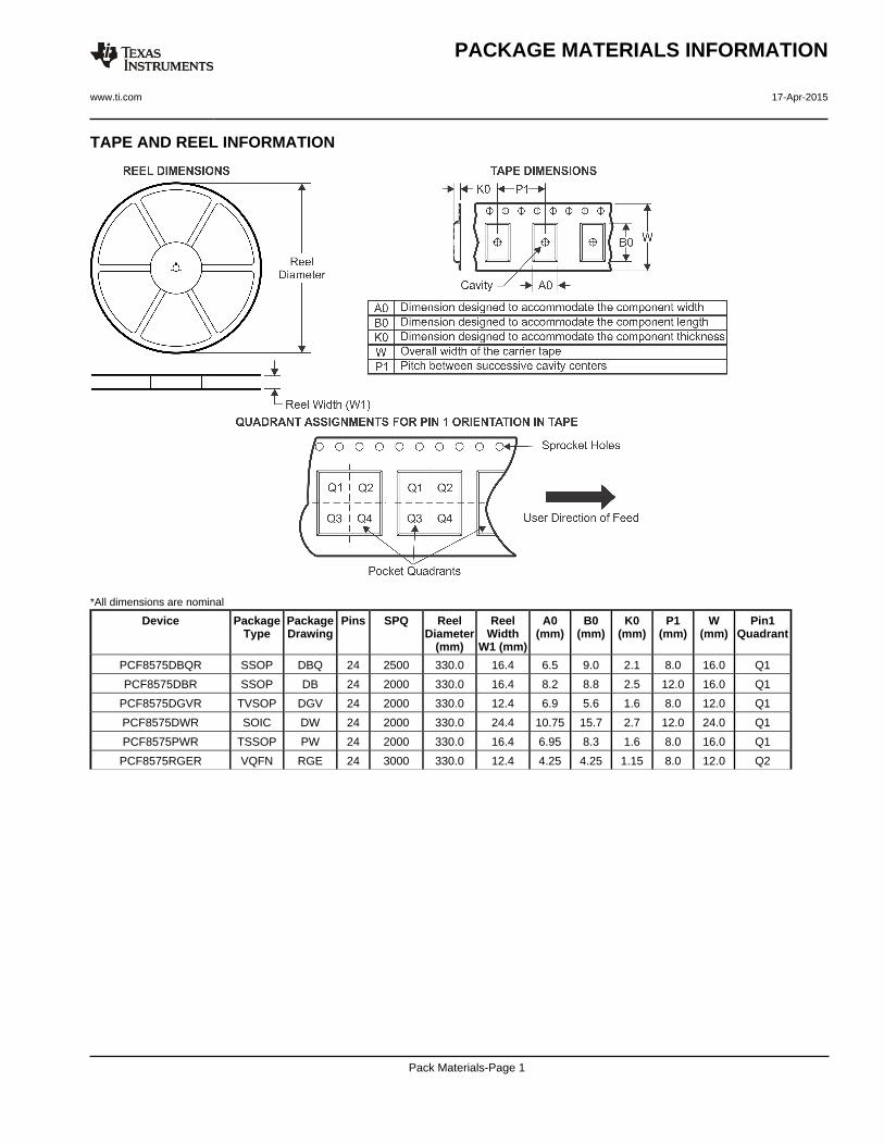
14 Mechanical, Packaging, and Orderable InformationThe following pages include mechanical packaging and orderable information. This information is the mostcurrent data available for the designated devices. This data is subject to change without notice and revision ofthis document. For browser based versions of this data sheet, refer to the left hand navigation.
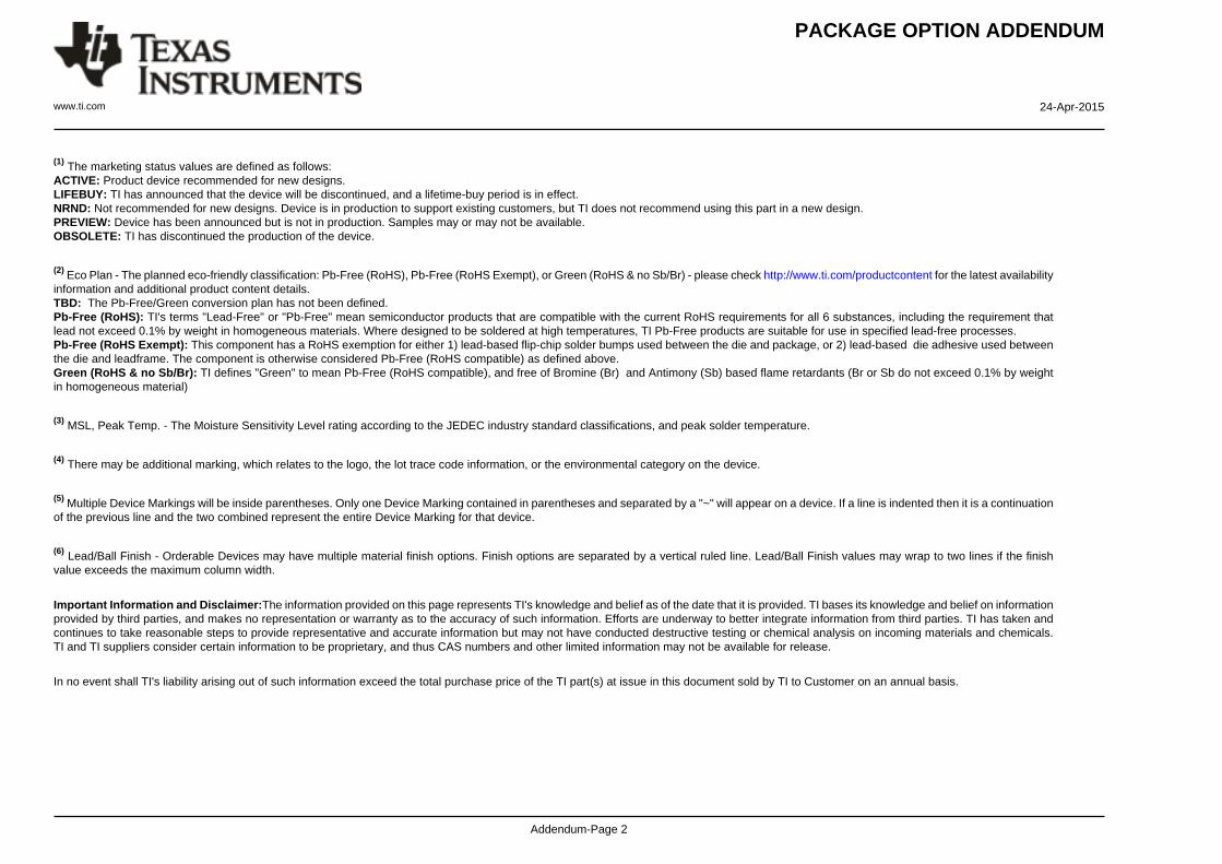
(1) The marketing status values are defined as follows:ACTIVE: Product device recommended for new designs.LIFEBUY: TI has announced that the device will be discontinued, and a lifetime-buy period is in effect.NRND: Not recommended for new designs. Device is in production to support existing customers, but TI does not recommend using this part in a new design.PREVIEW: Device has been announced but is not in production. Samples may or may not be available.OBSOLETE: TI has discontinued the production of the device.
(2) Eco Plan - The planned eco-friendly classification: Pb-Free (RoHS), Pb-Free (RoHS Exempt), or Green (RoHS & no Sb/Br) - please check http://www.ti.com/productcontent for the latest availabilityinformation and additional product content details.TBD: The Pb-Free/Green conversion plan has not been defined.Pb-Free (RoHS): TI's terms "Lead-Free" or "Pb-Free" mean semiconductor products that are compatible with the current RoHS requirements for all 6 substances, including the requirement thatlead not exceed 0.1% by weight in homogeneous materials. Where designed to be soldered at high temperatures, TI Pb-Free products are suitable for use in specified lead-free processes.Pb-Free (RoHS Exempt): This component has a RoHS exemption for either 1) lead-based flip-chip solder bumps used between the die and package, or 2) lead-based die adhesive used betweenthe die and leadframe. The component is otherwise considered Pb-Free (RoHS compatible) as defined above.Green (RoHS & no Sb/Br): TI defines "Green" to mean Pb-Free (RoHS compatible), and free of Bromine (Br) and Antimony (Sb) based flame retardants (Br or Sb do not exceed 0.1% by weightin homogeneous material)
(3) MSL, Peak Temp. - The Moisture Sensitivity Level rating according to the JEDEC industry standard classifications, and peak solder temperature.
(4) There may be additional marking, which relates to the logo, the lot trace code information, or the environmental category on the device.
(5) Multiple Device Markings will be inside parentheses. Only one Device Marking contained in parentheses and separated by a "~" will appear on a device. If a line is indented then it is a continuationof the previous line and the two combined represent the entire Device Marking for that device.
(6) Lead/Ball Finish - Orderable Devices may have multiple material finish options. Finish options are separated by a vertical ruled line. Lead/Ball Finish values may wrap to two lines if the finishvalue exceeds the maximum column width.
Important Information and Disclaimer:The information provided on this page represents TI's knowledge and belief as of the date that it is provided. TI bases its knowledge and belief on informationprovided by third parties, and makes no representation or warranty as to the accuracy of such information. Efforts are underway to better integrate information from third parties. TI has taken andcontinues to take reasonable steps to provide representative and accurate information but may not have conducted destructive testing or chemical analysis on incoming materials and chemicals.TI and TI suppliers consider certain information to be proprietary, and thus CAS numbers and other limited information may not be available for release.
In no event shall TI's liability arising out of such information exceed the total purchase price of the TI part(s) at issue in this document sold by TI to Customer on an annual basis.
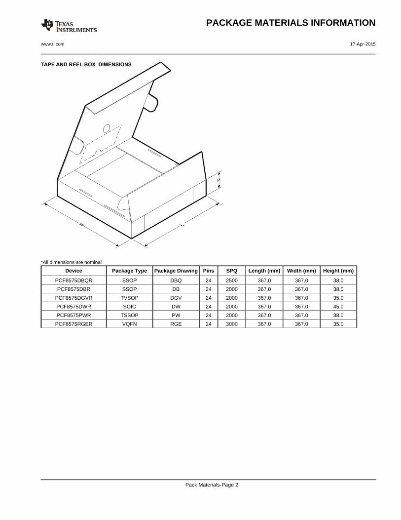
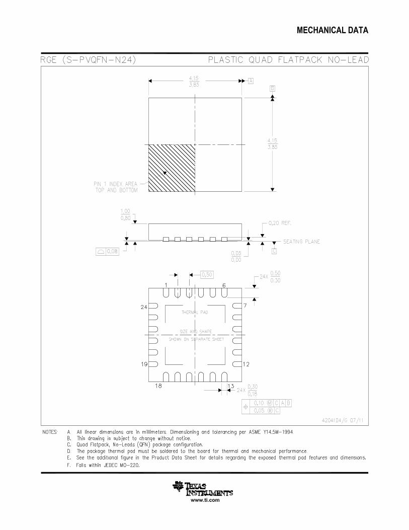
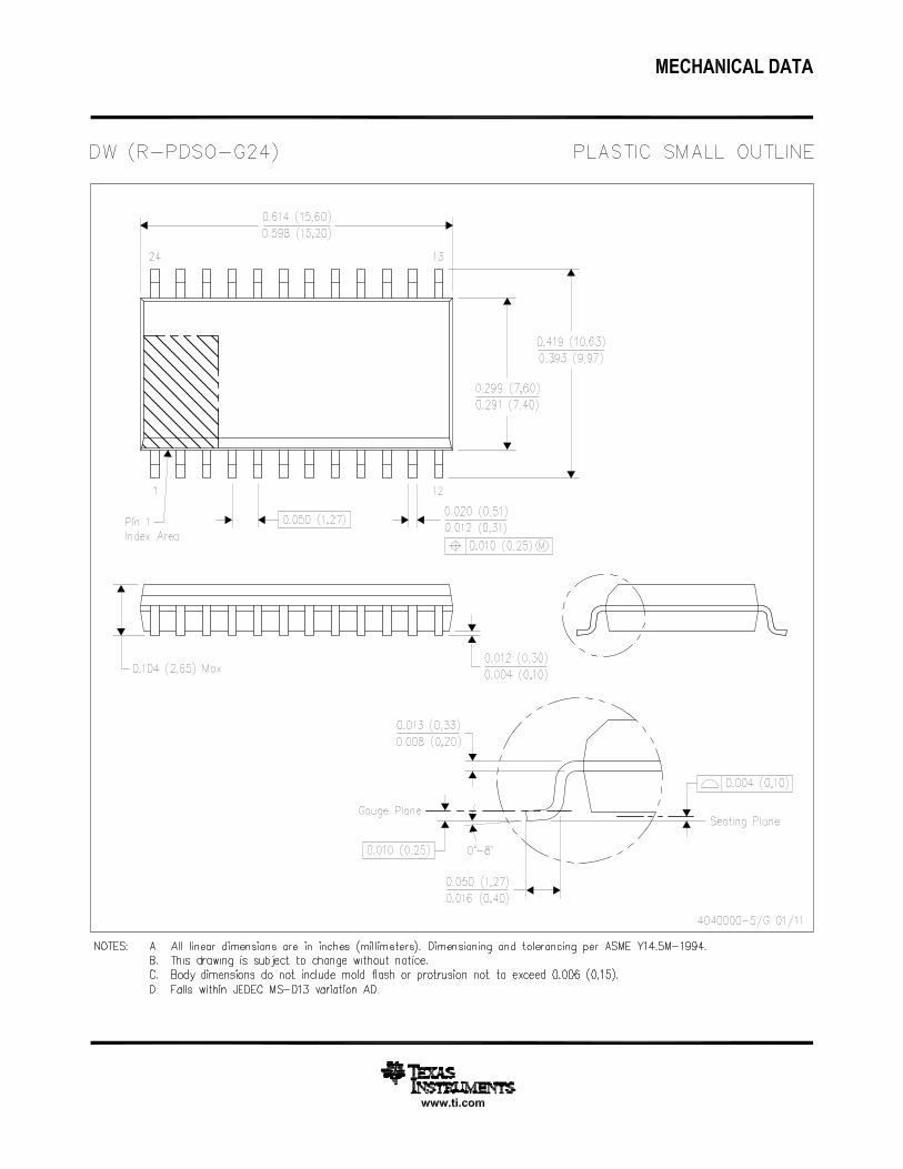
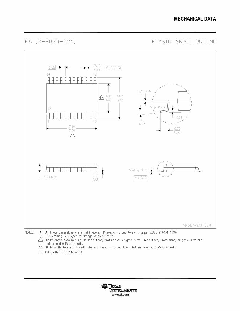
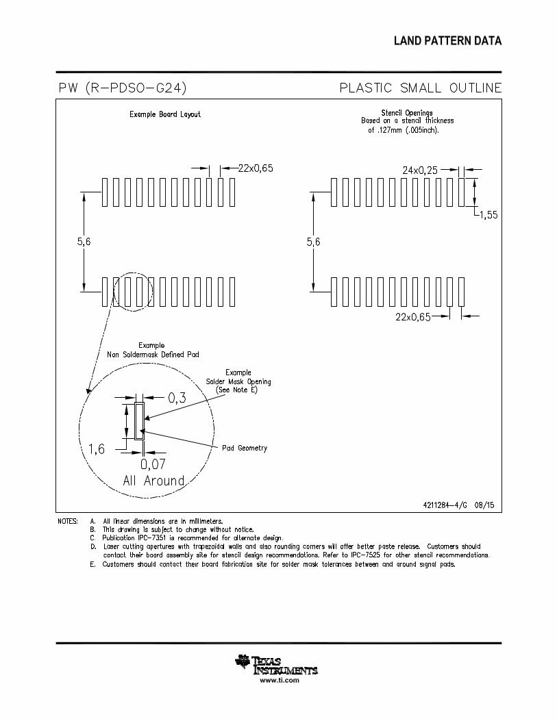
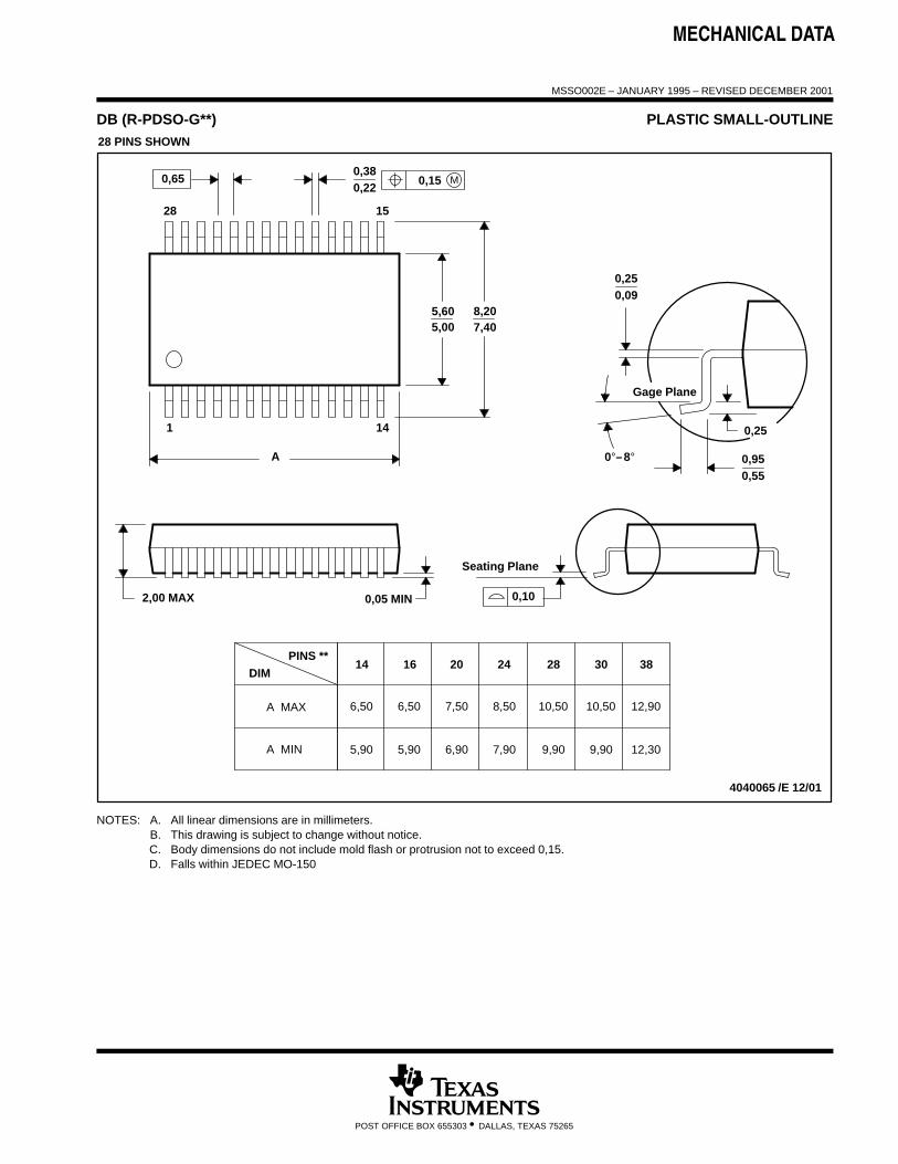
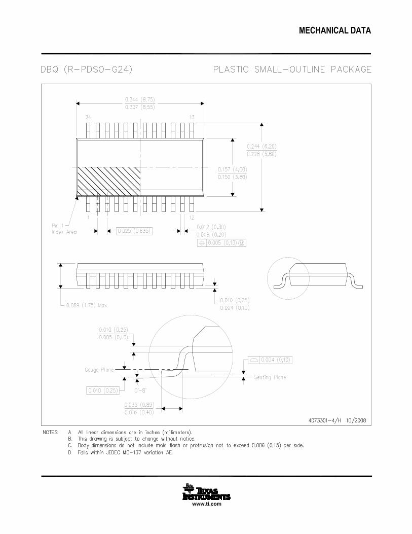
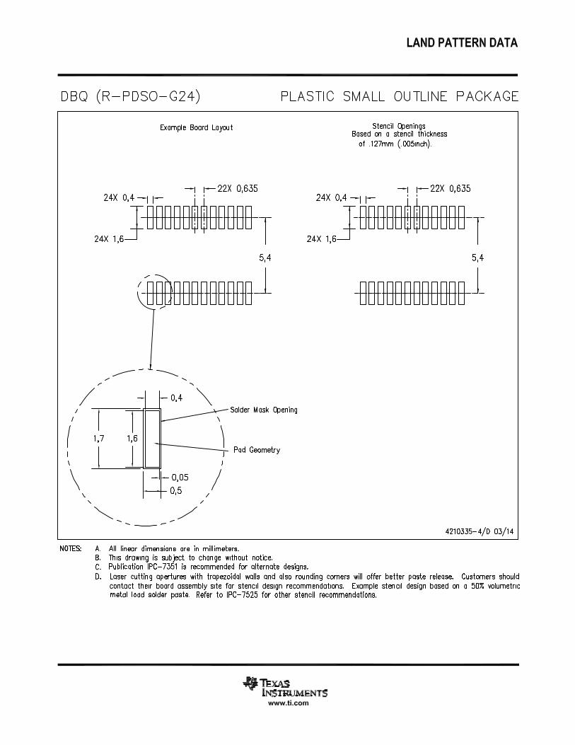
NOTES: A. All linear dimensions are in millimeters.B. This drawing is subject to change without notice.C. Body dimensions do not include mold flash or protrusion not to exceed 0,15.D. Falls within JEDEC MO-150
IMPORTANT NOTICE
Texas Instruments Incorporated (TI) reserves the right to make corrections, enhancements, improvements and other changes to itssemiconductor products and services per JESD46, latest issue, and to discontinue any product or service per JESD48, latest issue. Buyersshould obtain the latest relevant information before placing orders and should verify that such information is current and complete.TI’s published terms of sale for semiconductor products (http://www.ti.com/sc/docs/stdterms.htm) apply to the sale of packaged integratedcircuit products that TI has qualified and released to market. Additional terms may apply to the use or sale of other types of TI products andservices.Reproduction of significant portions of TI information in TI data sheets is permissible only if reproduction is without alteration and isaccompanied by all associated warranties, conditions, limitations, and notices. TI is not responsible or liable for such reproduceddocumentation. Information of third parties may be subject to additional restrictions. Resale of TI products or services with statementsdifferent from or beyond the parameters stated by TI for that product or service voids all express and any implied warranties for theassociated TI product or service and is an unfair and deceptive business practice. TI is not responsible or liable for any such statements.Buyers and others who are developing systems that incorporate TI products (collectively, “Designers”) understand and agree that Designersremain responsible for using their independent analysis, evaluation and judgment in designing their applications and that Designers havefull and exclusive responsibility to assure the safety of Designers' applications and compliance of their applications (and of all TI productsused in or for Designers’ applications) with all applicable regulations, laws and other applicable requirements. Designer represents that, withrespect to their applications, Designer has all the necessary expertise to create and implement safeguards that (1) anticipate dangerousconsequences of failures, (2) monitor failures and their consequences, and (3) lessen the likelihood of failures that might cause harm andtake appropriate actions. Designer agrees that prior to using or distributing any applications that include TI products, Designer willthoroughly test such applications and the functionality of such TI products as used in such applications.TI’s provision of technical, application or other design advice, quality characterization, reliability data or other services or information,including, but not limited to, reference designs and materials relating to evaluation modules, (collectively, “TI Resources”) are intended toassist designers who are developing applications that incorporate TI products; by downloading, accessing or using TI Resources in anyway, Designer (individually or, if Designer is acting on behalf of a company, Designer’s company) agrees to use any particular TI Resourcesolely for this purpose and subject to the terms of this Notice.TI’s provision of TI Resources does not expand or otherwise alter TI’s applicable published warranties or warranty disclaimers for TIproducts, and no additional obligations or liabilities arise from TI providing such TI Resources. TI reserves the right to make corrections,enhancements, improvements and other changes to its TI Resources. TI has not conducted any testing other than that specificallydescribed in the published documentation for a particular TI Resource.Designer is authorized to use, copy and modify any individual TI Resource only in connection with the development of applications thatinclude the TI product(s) identified in such TI Resource. NO OTHER LICENSE, EXPRESS OR IMPLIED, BY ESTOPPEL OR OTHERWISETO ANY OTHER TI INTELLECTUAL PROPERTY RIGHT, AND NO LICENSE TO ANY TECHNOLOGY OR INTELLECTUAL PROPERTYRIGHT OF TI OR ANY THIRD PARTY IS GRANTED HEREIN, including but not limited to any patent right, copyright, mask work right, orother intellectual property right relating to any combination, machine, or process in which TI products or services are used. Informationregarding or referencing third-party products or services does not constitute a license to use such products or services, or a warranty orendorsement thereof. Use of TI Resources may require a license from a third party under the patents or other intellectual property of thethird party, or a license from TI under the patents or other intellectual property of TI.TI RESOURCES ARE PROVIDED “AS IS” AND WITH ALL FAULTS. TI DISCLAIMS ALL OTHER WARRANTIES ORREPRESENTATIONS, EXPRESS OR IMPLIED, REGARDING RESOURCES OR USE THEREOF, INCLUDING BUT NOT LIMITED TOACCURACY OR COMPLETENESS, TITLE, ANY EPIDEMIC FAILURE WARRANTY AND ANY IMPLIED WARRANTIES OFMERCHANTABILITY, FITNESS FOR A PARTICULAR PURPOSE, AND NON-INFRINGEMENT OF ANY THIRD PARTY INTELLECTUALPROPERTY RIGHTS. TI SHALL NOT BE LIABLE FOR AND SHALL NOT DEFEND OR INDEMNIFY DESIGNER AGAINST ANY CLAIM,INCLUDING BUT NOT LIMITED TO ANY INFRINGEMENT CLAIM THAT RELATES TO OR IS BASED ON ANY COMBINATION OFPRODUCTS EVEN IF DESCRIBED IN TI RESOURCES OR OTHERWISE. IN NO EVENT SHALL TI BE LIABLE FOR ANY ACTUAL,DIRECT, SPECIAL, COLLATERAL, INDIRECT, PUNITIVE, INCIDENTAL, CONSEQUENTIAL OR EXEMPLARY DAMAGES INCONNECTION WITH OR ARISING OUT OF TI RESOURCES OR USE THEREOF, AND REGARDLESS OF WHETHER TI HAS BEENADVISED OF THE POSSIBILITY OF SUCH DAMAGES.Unless TI has explicitly designated an individual product as meeting the requirements of a particular industry standard (e.g., ISO/TS 16949and ISO 26262), TI is not responsible for any failure to meet such industry standard requirements.Where TI specifically promotes products as facilitating functional safety or as compliant with industry functional safety standards, suchproducts are intended to help enable customers to design and create their own applications that meet applicable functional safety standardsand requirements. Using products in an application does not by itself establish any safety features in the application. Designers mustensure compliance with safety-related requirements and standards applicable to their applications. Designer may not use any TI products inlife-critical medical equipment unless authorized officers of the parties have executed a special contract specifically governing such use.Life-critical medical equipment is medical equipment where failure of such equipment would cause serious bodily injury or death (e.g., lifesupport, pacemakers, defibrillators, heart pumps, neurostimulators, and implantables). Such equipment includes, without limitation, allmedical devices identified by the U.S. Food and Drug Administration as Class III devices and equivalent classifications outside the U.S.TI may expressly designate certain products as completing a particular qualification (e.g., Q100, Military Grade, or Enhanced Product).Designers agree that it has the necessary expertise to select the product with the appropriate qualification designation for their applicationsand that proper product selection is at Designers’ own risk. Designers are solely responsible for compliance with all legal and regulatoryrequirements in connection with such selection.Designer will fully indemnify TI and its representatives against any damages, costs, losses, and/or liabilities arising out of Designer’s non-compliance with the terms and provisions of this Notice.