Page 1
Page 1
PCI Express®• PCI Express : Where is it used in
computers?
• DUTs and J-BERT match
• Testing PCI Express
• PCIe 2 theory
• realization of RX-tests w/ J-BERT-A
• PCIe 3, another outlook
PCI-SIG and the PCI SIG design marks are registered
trademarks and/or service marks of PCI-SIG.
Page 2
Page 2
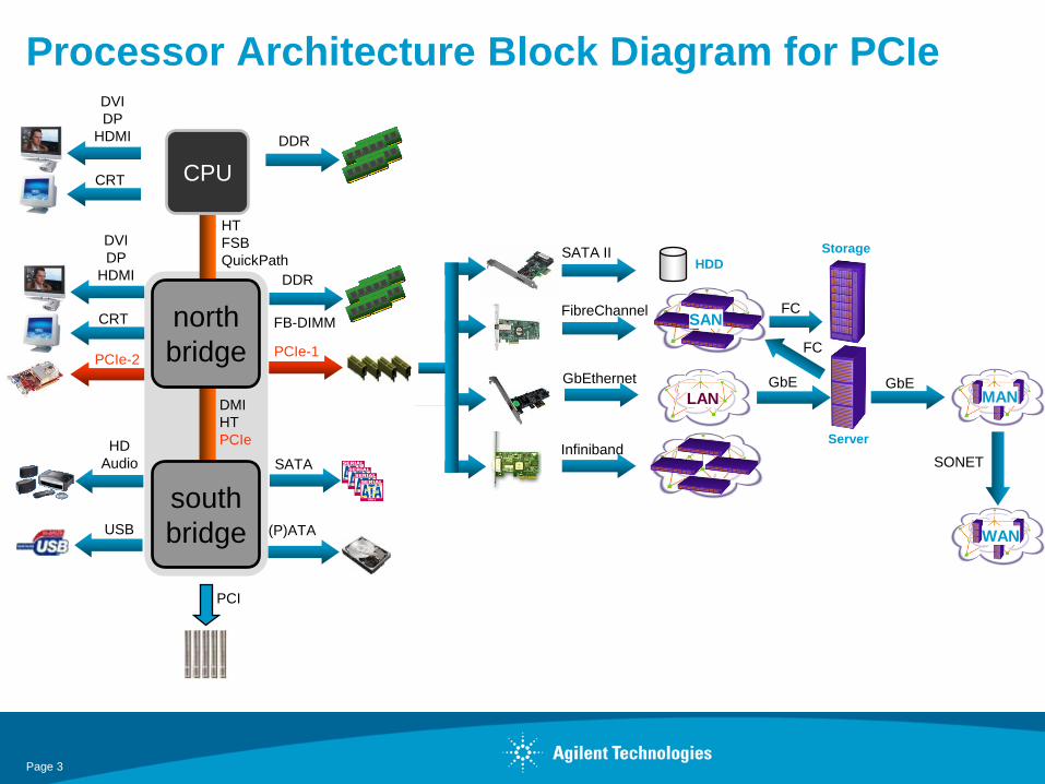
Processor Architecture Block Diagram for PCIe
PCI express
PCI express
Page 3
Page 3
CPU
north
bridge
south
bridge
HT
FSB
QuickPath
PCIe-2
FB-DIMM
PCIe-1
HD
Audio
USB
SATA
(P)ATA
PCI
DMI
HT
PCIe
DVI
DP
HDMI
CRT
DDR
SATA II
Infiniband
FibreChannel
GbEthernet
HDD
SAN
LAN
4Gb/s
Server
Storage
GbE
FC
FC
MANGbE
WAN
SONET
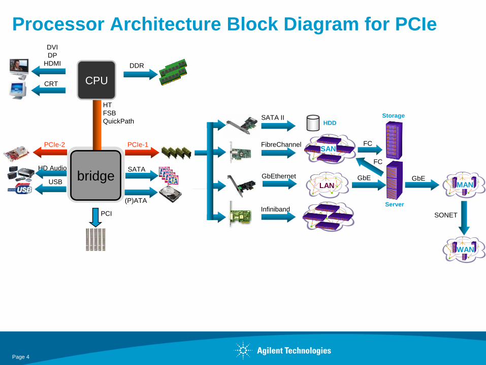
Processor Architecture Block Diagram for PCIeDVI
DP
HDMI
CRT
DDR
Page 4
Page 4
CPU
bridge
HT
FSB
QuickPath
PCIe-2 PCIe-1
HD Audio
USB
SATA
(P)ATA
PCI
SATA II
Infiniband
FibreChannel
GbEthernet
HDD
SAN
LAN
4Gb/s
Server
Storage
GbE
FC
FC
MANGbE
WAN
SONET
Processor Architecture Block Diagram for PCIeDVI
DP
HDMI
CRT
DDR
Page 5
Page 5
Testing PCI Express
Electrical Layer
Page 6
Page 6
Physical Layer Measurements
PCI Express Electrical Layer Test
Jitter transfer
PLL or CDR frequency
response measurements
RX sensitivity and
jitter tolerance test
Infiniium
ScopeJ-BERT
TX waveform
characterization and jitter
decomposition
Page 7
Page 7
DUTs and Tests
DUT mandatory test /
recommended tests
relevant spec
I/Os of test chips TX, RX, jitter transfer PCIe base spec
I/Os of final ASICs
Add in cards (graphic) TX, jitter transfer
RX sensitivity w/
stressed eye
CEM card spec
Motherboards
Page 8
Page 8
Which Tests, Addressed When and How
Test Now
RX sensitivity
and jitter
tolerance
J-BERT A + 81150A &
15431A for correct RJ
spectrum
trace #2 for ISI / DJ
TX waveform
tests
Scope
TX jitter
transfer
Scope
Page 9
Page 9
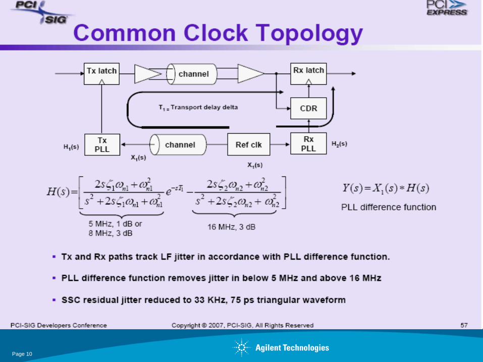
The Theory Behind the Specs
Page 14
Page 14
RX Jitter Tolerance Specs
Based Upon Channel Behavior: DJ (ISI+PJ)
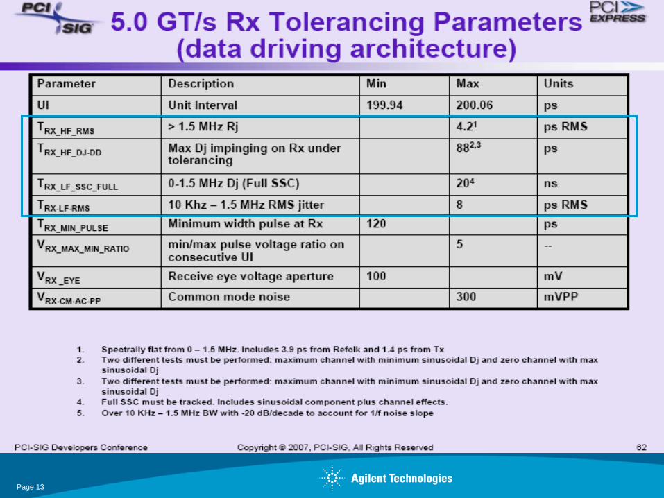
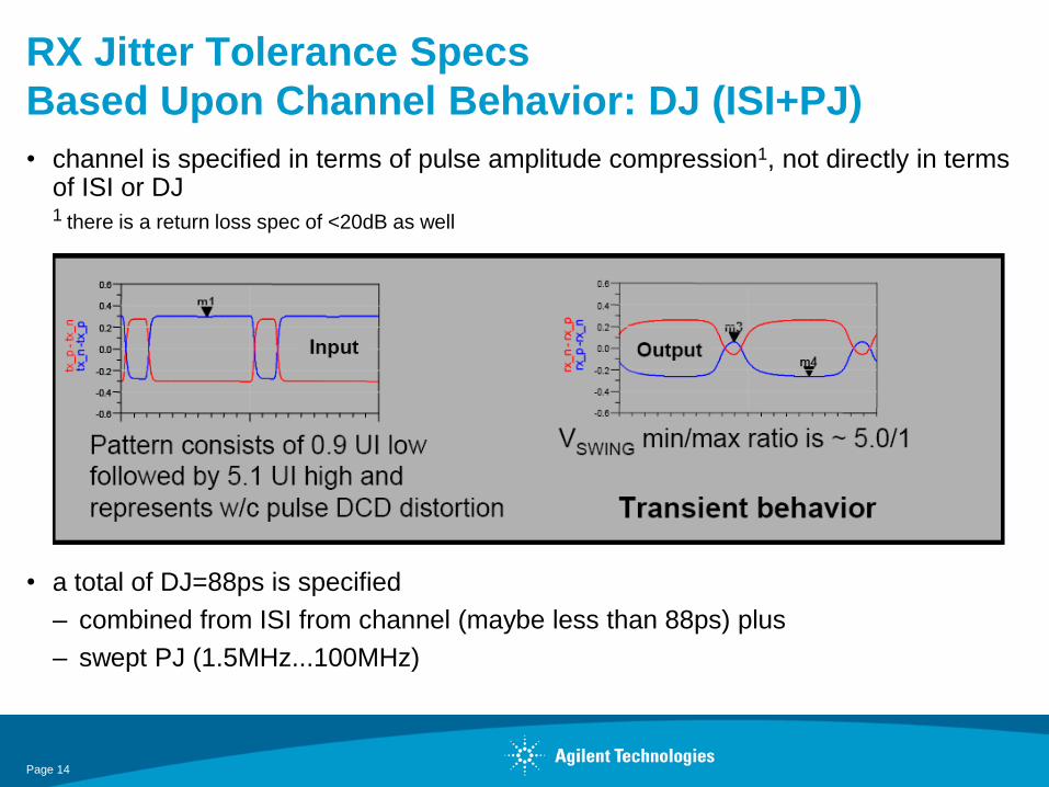
• channel is specified in terms of pulse amplitude compression1, not directly in terms of ISI or DJ1 there is a return loss spec of <20dB as well
• a total of DJ=88ps is specified
– combined from ISI from channel (maybe less than 88ps) plus
– swept PJ (1.5MHz...100MHz)
Page 15
Page 15
Trace # 2 OK for PCI Express 2.0
pattern:
1111 1011 1111 1111
0000 0100 0000 0000
normal only, trig / 16
levels of lone 1 (0) are
about 20% of those
of long duration.
Levels of long duration
are equivalent to
those of w/o channel
Page 16
Page 16
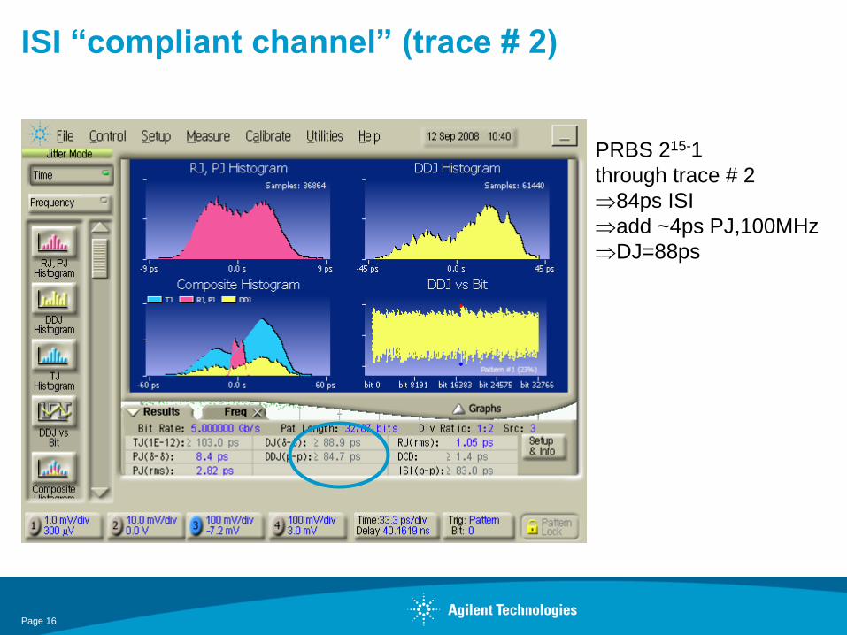
ISI “compliant channel” (trace # 2)
PRBS 215-1
through trace # 2
84ps ISI
add ~4ps PJ,100MHz
DJ=88ps
Page 17
Page 17
Summary: RX tolerance Jitter Specs (Base Spec)
common ref-clk
• RX sampling on (multiplied) ref clk
• RX w /DLL only
• SSC off: no phase error induced
• SSC on:
– small error (fempto seconds) due to path delay difference (!) but
– significant residual phase error due to potentially different transfer functions (BW and peaking) of TX and RX clock multiplying PLLs
data clocked (embedded clock)
• RX w/ PLL-CDR (using ref clock only until locked)
• SSC on or off
– common for TX and RX
– both TX’s use same ref clk
two different clocking architectures:
Com Ref-clk Data Clockedrms pp rms pp
SSC residual: 75 SSC 20 ns
RJ (?) HF 3.4 47.6 RJ (?) HF 4.2 58.8
LF 4.2 58.8 LF 8.0 112
RJ,sqrt sum 5.4 75.7 RJ,sqrt sum 9.0 126.5
DJ HF 88 DJ HF 88
“UHF”
total sqrt 150.7 - 238.7 total sqrt 126.5 - 214.5
Page 18
Page 18
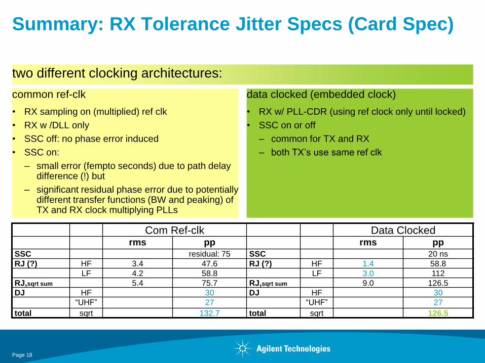
Summary: RX Tolerance Jitter Specs (Card Spec)
common ref-clk
• RX sampling on (multiplied) ref clk
• RX w /DLL only
• SSC off: no phase error induced
• SSC on:
– small error (fempto seconds) due to path delay difference (!) but
– significant residual phase error due to potentially different transfer functions (BW and peaking) of TX and RX clock multiplying PLLs
data clocked (embedded clock)
• RX w/ PLL-CDR (using ref clock only until locked)
• SSC on or off
– common for TX and RX
– both TX’s use same ref clk
two different clocking architectures:
Com Ref-clk Data Clockedrms pp rms pp
SSC residual: 75 SSC 20 ns
RJ (?) HF 3.4 47.6 RJ (?) HF 1.4 58.8
LF 4.2 58.8 LF 3.0 112
RJ,sqrt sum 5.4 75.7 RJ,sqrt sum 9.0 126.5
DJ HF 30 DJ HF 30
“UHF” 27 “UHF” 27
total sqrt 132.7 total sqrt 126.5
Page 19
Page 19
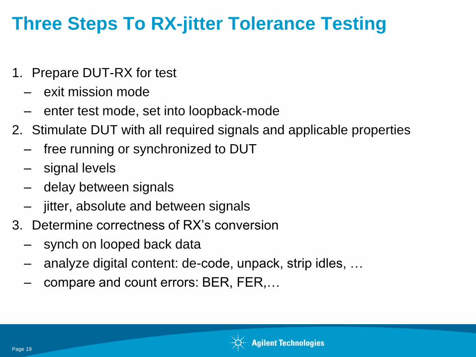
Three Steps To RX-jitter Tolerance Testing
1. Prepare DUT-RX for test
– exit mission mode
– enter test mode, set into loopback-mode
2. Stimulate DUT with all required signals and applicable properties
– free running or synchronized to DUT
– signal levels
– delay between signals
– jitter, absolute and between signals
3. Determine correctness of RX’s conversion
– synch on looped back data
– analyze digital content: de-code, unpack, strip idles, …
– compare and count errors: BER, FER,…
Page 20
Page 20
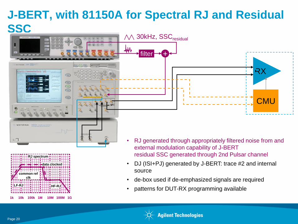
RX
J-BERT, with 81150A for Spectral RJ and Residual
SSC
• RJ generated through appropriately filtered noise from and
external modulation capability of J-BERT
residual SSC generated through 2nd Pulsar channel
• DJ (ISI+PJ) generated by J-BERT: trace #2 and internal
source
• de-box used if de-emphasized signals are required
• patterns for DUT-RX programming available
filter
CMU
+
30kHz, SSCresidual
1k 10k 100k 1M 10M 100M 1G
RJ spectrum
data clocked
common ref
clk
LF-RJ HF-RJ
Page 21
Page 21
Outlook PCIe-3
Page 22
Page 22
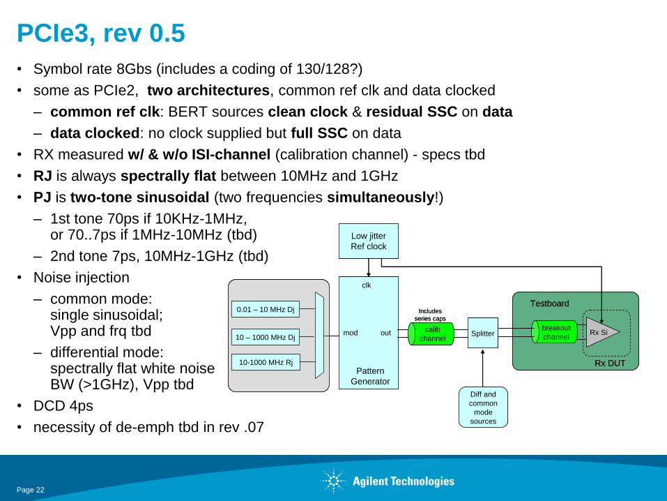
PCIe3, rev 0.5
• Symbol rate 8Gbs (includes a coding of 130/128?)
• some as PCIe2, two architectures, common ref clk and data clocked
– common ref clk: BERT sources clean clock & residual SSC on data
– data clocked: no clock supplied but full SSC on data
• RX measured w/ & w/o ISI-channel (calibration channel) - specs tbd
• RJ is always spectrally flat between 10MHz and 1GHz
• PJ is two-tone sinusoidal (two frequencies simultaneously!)
– 1st tone 70ps if 10KHz-1MHz, or 70..7ps if 1MHz-10MHz (tbd)
– 2nd tone 7ps, 10MHz-1GHz (tbd)
• Noise injection
– common mode: single sinusoidal; Vpp and frq tbd
– differential mode: spectrally flat white noise BW (>1GHz), Vpp tbd
• DCD 4ps
• necessity of de-emph tbd in rev .07
breakout
channelRx Si
Rx DUT
Testboard
Low jitter
Ref clock
clk
mod out
Pattern
Generator
Splitter
Diff and
common
mode
sources
0.01 – 10 MHz Dj
10 – 1000 MHz Dj
10-1000 MHz Rj
calib
channel
Includes
series caps
breakout
channelRx Si
Rx DUT
Testboard
Low jitter
Ref clock
clk
mod out
Pattern
Generator
Splitter
Diff and
common
mode
sources
0.01 – 10 MHz Dj
10 – 1000 MHz Dj
10-1000 MHz Rj
0.01 – 10 MHz Dj
10 – 1000 MHz Dj
10-1000 MHz Rj
calib
channel
Includes
series caps