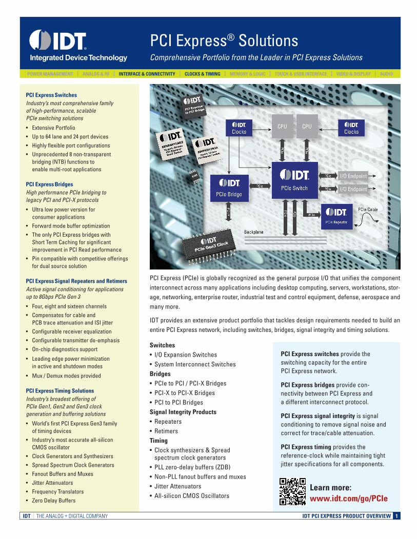
PCI Express Switches Industry’s most comprehensive family of high-performance, scalable PCIe switching solutions • Extensive Portfolio • Up to 64 lane and 24 port devices • Highly flexible port configurations • Unprecedented 8 non-transparent bridging (NTB) functions to enable multi-root applications PCI Express Bridges High performance PCIe bridging to legacy PCI and PCI-X protocols • Ultra low power version for consumer applications • Forward mode buffer optimization • The only PCI Express bridges with Short Term Caching for significant improvement in PCI Read performance • Pin compatible with competitive offerings for dual source solution PCI Express Signal Repeaters and Retimers Active signal conditioning for applications up to 8Gbps PCIe Gen 3 • Four, eight and sixteen channels • Compensates for cable and PCB trace attenuation and ISI jitter • Configurable receiver equalization • Configurable transmitter de-emphasis • On-chip diagnostics support • Leading edge power minimization in active and shutdown modes • Mux / Demux modes provided PCI Express Timing Solutions Industry’s broadest offering of PCIe Gen1, Gen2 and Gen3 clock generation and buffering solutions • World’s first PCI Express Gen3 family of timing devices • Industry’s most accurate all-silicon CMOS oscillator • Clock Generators and Synthesizers • Spread Spectrum Clock Generators • Fanout Buffers and Muxes • Jitter Attenuators • Frequency Translators • Zero Delay Buffers IDT | THE ANALOG + DIGITAL COMPANY IDT PCI EXPRESS PRODUCT OVERVIEW PCI Express (PCIe) is globally recognized as the general purpose I/O that unifies the component interconnect across many applications including desktop computing, servers, workstations, stor- age, networking, enterprise router, industrial test and control equipment, defense, aerospace and many more. IDT provides an extensive product portfolio that tackles design requirements needed to build an entire PCI Express network, including switches, bridges, signal integrity and timing solutions. PCI Express switches provide the switching capacity for the entire PCI Express network. PCI Express bridges provide con- nectivity between PCI Express and a different interconnect protocol. PCI Express signal integrity is signal conditioning to remove signal noise and correct for trace/cable attenuation. PCI Express timing provides the reference-clock while maintaining tight jitter specifications for all components. Learn more: www.idt.com/go/PCIe Switches • I/O Expansion Switches • System Interconnect Switches Bridges • PCIe to PCI / PCI-X Bridges • PCI-X to PCI-X Bridges • PCI to PCI Bridges Signal Integrity Products • Repeaters • Retimers Timing • Clock synthesizers & Spread spectrum clock generators • PLL zero-delay buffers (ZDB) • Non-PLL fanout buffers and muxes • Jitter Attenuators • All-silicon CMOS Oscillators Integrated DeviceTechnology 1 PCI Express ® Solutions Comprehensive Portfolio from the Leader in PCI Express Solutions POWER MANAGEMENT | ANALOG & RF | INTERFACE & CONNECTIVITY | CLOCKS & TIMING | MEMORY & LOGIC | TOUCH & USER INTERFACE | VIDEO & DISPLAY | AUDIO
POWER MANAGEMENT | ANALOG & RF | INTERFACE & CONNECTIVITY | CLOCKS & TIMING | MEMORY & LOGIC | TOUCH & USER INTERFACE | VIDEO & DISPLAY | AUDIO
DISCLAIMER Integrated Device Technology, Inc. (IDT) and its subsidiaries reserve the right to modify the products and/or specifications described herein at any time and at IDT’s sole discretion. All information in this document, including descriptions of product features and performance, is subject to change without notice. Performance specifications and the operating parameters of the described products are determined in the independent state and are not guaranteed to perform the same way when installed in customer products. The information contained herein is provided without representation or warranty of any kind, whether express or implied, including, but not limited to, the suitability of IDT’s products for any particular purpose, an implied warranty of merchantability, or non-infringement of the intellectual property rights of others. This document is presented only as a guide and does not convey any license under intellectual property rights of IDT or any third parties. IDT’s products are not intended for use in life support systems or similar devices where the failure or malfunction of an IDT product can be reasonably expected to significantly affect the health or safety of users. Anyone using an IDT product in such a manner does so at their own risk, absent an express, written agreement by IDT.
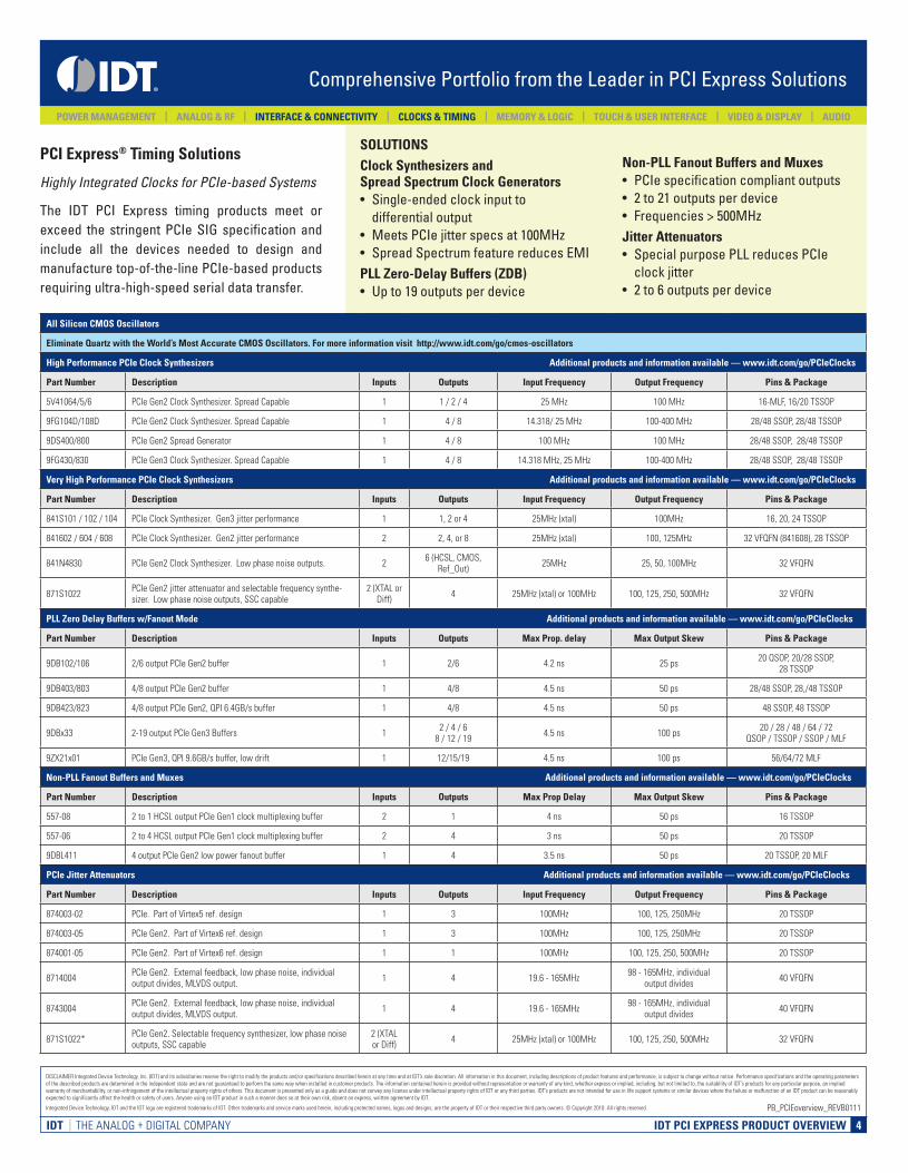
The IDT PCI Express timing products meet orexceed the stringent PCIe SIG specification andinclude all the devices needed to design andmanufacturetop-of-the-linePCIe-basedproductsrequiringultra-high-speedserialdatatransfer.
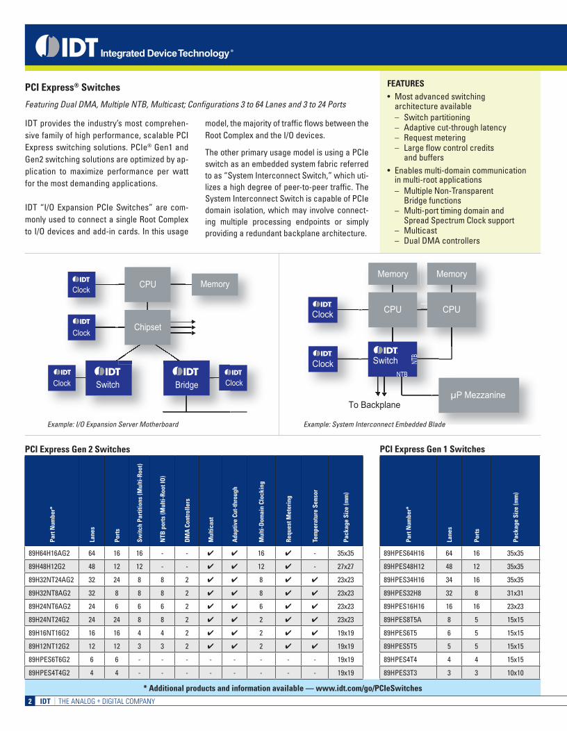
PCI Express Gen 2 Switches PCI Express Gen 1 Switches
IDT PCI EXPRESS PRODUCT OVERVIEW
Integrated Device Technology
PCI Express® Switches
Featuring Dual DMA, Multiple NTB, Multicast; Configurations 3 to 64 Lanes and 3 to 24 Ports
PCI Express Bridges
PCI Express Signal Integrity Products
IDTprovidestheindustry’smostcomprehen-sivefamilyofhighperformance,scalablePCIExpressswitchingsolutions.PCIe®Gen1andGen2switchingsolutionsareoptimizedbyap-plication to maximize performance per wattforthemostdemandingapplications.
IDT “I/O Expansion PCIe Switches” are com-monlyusedtoconnectasingleRootComplextoI/Odevicesandadd-incards.Inthisusage
TheotherprimaryusagemodelisusingaPCIeswitchasanembeddedsystemfabricreferredtoas“SystemInterconnectSwitch,”whichuti-lizesahighdegreeofpeer-to-peertraffic.TheSystemInterconnectSwitchiscapableofPCIedomain isolation,whichmay involveconnect-ing multiple processing endpoints or simplyprovidingaredundantbackplanearchitecture.
PCIe to PCI and PCI-X Bus Standards
Tocomplementtheswitchproducts,IDToffers bridges to connect PCIe to thePCI and PCI-X bus standards. A PCIebridgeisusedforbridgingdevicesthatuse the PCI/X interface to provide aPCIeconnectiontoahostprocessororrootcomplex.ApplicationsincludePCIeadapter cards, embedded computing,and motherboards to provide connec-tiontoPCI/XdevicesoradditionalPCI/Xexpansionslots.
PCIe Gen 3 and Gen2 Standards
With the increase of signal speeds in thecomputing, storage and communicationsapplications,systemdesigners increasinglyface signal integrity challenges. Signal In-tegrity Product (SIP) components providesignal conditioning for applications up to8Gbps, PCI Express 3.0, delivering signalquality over extended distances while of-feringsimplifieddesignbyalleviatingboardlayoutconstraints.
Thesedevicesincorporateadvancedreceiveequalizationandtransmitde-emphasiscapa-bilities, as well as diagnostic features thathelpIDTcustomersachieveasimplifiedde-signwithfastertime-to-market.Specifically,thedevicesdrivelongon-boardtraces,back-planetracesandcablestoexternaldevicestoensureoptimumsystemperformance.Thedevicesallofferpowersavingsmodesforthelowest-possiblepowerconsumption.
POWER MANAGEMENT | ANALOG & RF | INTERFACE & CONNECTIVITY | CLOCKS & TIMING | MEMORY & LOGIC | TOUCH & USER INTERFACE | VIDEO & DISPLAY | AUDIO
DISCLAIMER Integrated Device Technology, Inc. (IDT) and its subsidiaries reserve the right to modify the products and/or specifications described herein at any time and at IDT’s sole discretion. All information in this document, including descriptions of product features and performance, is subject to change without notice. Performance specifications and the operating parameters of the described products are determined in the independent state and are not guaranteed to perform the same way when installed in customer products. The information contained herein is provided without representation or warranty of any kind, whether express or implied, including, but not limited to, the suitability of IDT’s products for any particular purpose, an implied warranty of merchantability, or non-infringement of the intellectual property rights of others. This document is presented only as a guide and does not convey any license under intellectual property rights of IDT or any third parties. IDT’s products are not intended for use in life support systems or similar devices where the failure or malfunction of an IDT product can be reasonably expected to significantly affect the health or safety of users. Anyone using an IDT product in such a manner does so at their own risk, absent an express, written agreement by IDT.
The IDT PCI Express timing products meet orexceed the stringent PCIe SIG specification andinclude all the devices needed to design andmanufacturetop-of-the-linePCIe-basedproductsrequiringultra-high-speedserialdatatransfer.


![PCI Express to PCI-X Reversible Bridge · PDF filePCI Express to PCI-X Reversible Bridge Revision 2.5 ... 7.5.135 bit [30] of Replay and ... 6 PCI EXPRESS FUNCTIONAL OVERVIEW](https://static.documents.pub/doc/80x56/5ab0dd047f8b9a00728b95ba/pci-express-to-pci-x-reversible-bridge-express-to-pci-x-reversible-bridge-revision.jpg)


