22
Application Note PCIE-RA Series Final Inch™ Designs in PCI Express® Applications Generation 3 - 8.0 GT/s Copyrights and Trademarks Copyright © 2016 Samtec, Inc.

Application Note
PCIE-RA Series Final Inch™ Designs in PCI Express® Applications
Generation 3 - 8.0 GT/s
Copyrights and Trademarks Copyright © 2016 Samtec, Inc.

Application Note
Series: PCIE-RA Standard: PCI Express®, Generation 3, 8 GT/s
Revision Date: 10/24/2016 1 Copyright 2016 Samtec
COPYRIGHTS, TRADEMARKS, and PATENTS Final Inch™ is a trademark of Samtec, Inc. Other product names used herein are trademarks of their respective owners. All information and material in this publication are property of Samtec, Inc. All related rights are reserved. Samtec, Inc. does not authorize customers to make copies of the content for any use. Terms of Use Use of this publication is limited to viewing the pages for evaluation or purchase. No permission is granted to the user to copy, print, distribute, transmit, display in public, or modify the contents of this document in any way. Disclaimer The information in this publication may change without notice. All materials published here are “As Is” and without implied or expressed warranties. Samtec, Inc. does not warrant this publication will be without error, or that defects will be corrected. Samtec, Inc. makes every effort to present our customers an excellent and useful publication, but we do not warrant or represent the use of the materials here in terms of their accuracy, reliability or otherwise. Therefore, you agree that all access and use of this publication's content is at your own risk. NEITHER SAMTEC, INC. NOR ANY PARTY INVOLVED IN CREATING, PRODUCING, OR DELIVERING THIS PUBLICATION SHALL BE LIABLE FOR ANY DIRECT, INCIDENTAL, CONSEQUENTIAL, INDIRECT, OR PUNITIVE DAMAGES ARISING OUT OF YOUR ACCESS, USE OR INABILITY TO ACCESS OR USE THIS PUBLICATION, OR ANY ERRORS OR OMISSIONS IN ITS CONTENT.

Application Note
Series: PCIE-RA Standard: PCI Express®, Generation 3, 8 GT/s
Revision Date: 10/24/2016 2 Copyright 2016 Samtec
Abstract
The PCI Express® is primarily intended as a high performance serial interface targeted for use in desktop, mobile, workstation, server, communications platforms, and embedded devices. As with any modern high speed PCB design, the performance of an actual PCI Express® interconnect is highly dependent on the implementation. Recent advances in technology have allowed PCI Express® designs to reliably reach 8.0 GT/s using common PCB materials and advanced Tx and Rx equalization techniques. This paper describes a statistical simulation compliance method applied to proven Samtec Final Inch™ designs. This application note is intended to help engineers deploy systems of two PCB cards mated through Samtec’s family of high speed electrical connectors. To demonstrate the feasibility of using Samtec’s PCIE-Right Angle (RA) card socket with standard FR4 epoxy PCBs, statistical simulation will be used to characterize the full Tx die-to-Rx die PCIE 8.0 GT/s channel, utilizing Samtec Final Inch™ s-parameter modeling of the connector and complete interconnect channel, including all aggressor crosstalk impacts.

Application Note
Series: PCIE-RA Standard: PCI Express®, Generation 3, 8 GT/s
Revision Date: 10/24/2016 3 Copyright 2016 Samtec
Introduction Samtec has developed a full line of connector products that are designed to support serial speeds up to 8 GT/s, the maximum transfer rate of each PCI Express® data lane. Working with Teraspeed Consulting, they have developed a complete breakout and routing solution for each member of the Samtec line of high speed connectors, called Final Inch™. To demonstrate the feasibility of using Samtec PCIE-RA connectors in PCI Express® applications with standard FR4 epoxy PCBs, full s-parameter modeling of the channel, along with statistical simulation techniques, will be used to sweep various trace lengths across the design space to show a final compliance region.
The PCI Express® Specification PCI Express® 8.0 GT/s links are based on recent advances in signal processing technology using advanced Tx and Rx equalization. A PCI Express® link is comprised of a dual-simplex communications channel between two components physically consisting of two low-voltage, differential signal pairs. The PCI Express® Base Specification defines one half of a link (one transmitter and receiver) as an electrical sub-block. The design model used for this paper is of three electrical sub-blocks operating in tandem, one the victim surrounded by 2 aggressors, with all bit streams heading in the same direction. Detailed specifications for an electrical sub-block can be found starting in Section 4.3 of the PCI Express® Base Specification and will be referred to throughout the rest of this paper. Detailed channel specifications start in Sub-section 4.3.6. Channel compliance testing requirements of subsection 4.3.6.4 for 8.0 GT/s were adhered to for these simulations. See PCI Express® Base Specification Revision 3.0 for more details.

Application Note
Series: PCIE-RA Standard: PCI Express®, Generation 3, 8 GT/s
Revision Date: 10/24/2016 4 Copyright 2016 Samtec
The Simulation Model Figure 1 shows the mated Samtec PCIE-RA card socket used in a typical multi-segment channel with a source adapter residing on a motherboard and a target adapter residing on an add-in card. The test circuit is modeled as:
Keysight’s Advanced Design System Tx and Rx modules that correlate to the Tx and Rx package models released by the PCI Special Interest Group, and defined in Section 4.3.6 - Channel Specification - of the PCI Express® Base Specification, Rev 3.0.
A variable length interconnect trace segment on the source adapter, with and without a 200 nF capacitor
A variable length interconnect trace segment on the target adapter. A mated Samtec PCIE-RA connector touchstone s-parameter model.
Figure 1 - PCI Express® 8 .0 GT/s Test Configuration
Segment topology of the source and target adapters were swept in multiple ways to determine the limits of compliant channel operation, and whether any sensitivity exists.
1. All combinations of 0.1" to 1" in steps of 0.1" for both the source and target adapter.
2. Source length = target length swept from 1" to 20" to determine the entire reliable operation limit of the channel.
3. Source length swept from 1" to 30" with the target length set at 4", which is the typical maximum length for PCIE add-in cards.

Application Note
Series: PCIE-RA Standard: PCI Express®, Generation 3, 8 GT/s
Revision Date: 10/24/2016 5 Copyright 2016 Samtec
For sweep configuration #3 additional simulations were performed with the addition of 200 nF DC blocking capacitors, to model additional signal quality degradation. All traces were modeled as microstrip on FR4 with the following parameters:
FR4 is modeled using a Svensson/Djordjevic causal model that has a broadband response that is faithful to measured results from DC to greater than 20 GHz, using the following parameters:
o Er = 4.2 @ 1 GHz o Loss Tangent = 0.02 @ 1 GHz
Copper is modeled as follows to reflect the reduced conductivity of copper
foil used in PCB fabrication: o Conductivity = 4.5E+7 S-m o Surface roughness = 0.6 micron
Traces are differential microstrip with the following geometry: o 100 ohm differential impedance o 4.25 mil trace width o 2.0 mil trace copper thickness o 5.75 mil center-to-center spacing o 4.4 mil FR4 dielectric thickness o No differential coupling to neighboring differential channels
These parameters reflect typical trace geometries and material parameters used in Samtec Final Inch™ test boards. Other trace geometries or materials will lead to different results than shown here. However, if reasonable care is made to stay well within the design space and guidelines provided in this document, it is possible to build robust PCIE 8.0 GT/s channels with limited additional simulation verification.

Application Note
Series: PCIE-RA Standard: PCI Express®, Generation 3, 8 GT/s
Revision Date: 10/24/2016 6 Copyright 2016 Samtec
The Simulation Environment The PCI Express® Base specification requires that 8.0 GT/s channel compliance be performed utilizing a die-to-die interconnect model, including the Tx and Rx packages. "The model shall include both victim and a sufficient number of aggressor paths to accurately capture the channel crosstalk effects. Using the Tx voltage and jitter limits defined in the transmitter specification ... it is possible to transform these parameters to what would appear at the die pad of a Tx" [sic]. As shown in Figure 2, the output of the simulation is actually the eye as it appears at the input of the Rx sample latch.
Figure 2 - PCI Express® 8 .0 GT/s Flow Diagram for Channel Tolerance
The PCI Special Interest Group (SIG) provides an open source statistical eye simulator (seasim v0.46) that may be used to implement the following necessary simulation and modeling requirements:
Channel characteristics defined as s-parameters. Behavioral Tx and Rx package models. Transmitter jitter and voltage. Transmitter and receiver termination impedance of 2 x 50 ohm. Time domain representation of the end-to-end connectivity. Behavioral Tx equalization. Behavioral Rx continuous time linear equalizer (CTLE). Behavioral Rx digital feedback equalizer (DFE). Optimization of Tx equalization and Rx DFE/CTLE settings. Statistical treatment of jitter. Statistically defined output eye width and eye height.

Application Note
Series: PCIE-RA Standard: PCI Express®, Generation 3, 8 GT/s
Revision Date: 10/24/2016 7 Copyright 2016 Samtec
For this application note, Keysight’s Advanced Designed System 2016.01 (ADS2016) software simulation tool is used to accomplish the simulation tasks. Templates were developed within ADS to automate the analysis so that channel components can be easily replaced. The results from SEASIM and ADS are the same provided the same source jitter and equalization settings are used. The ADS templates require the following channel definitions:
Definition of input S-parameter files to be used in the simulations. o Samtec PCIE-RA mated connector o Tx Package o Rx Package o FR4 Microstrip Differential Trace o 200 nF 0403 capacitor
Definition of Tx segment 1 and Rx segment 2 trace lengths to be
simulated. Iterative processing of all trace length cases using the ADS2016 batch
simulation mode.
Compliance Eye Mask Figure 3 shows the 8.0 GT/s channel compliance eye mask. The ADS2016 channel simulator and Samtec modeling provide all necessary inputs required to generate the statistical eye necessary to test against the eye mask pass/fail requirements. Although the specification allows for a minimum measured eye height of 25 mV P-P, we will de-rate the specification to 50 mV P-P for the purposes of this study, to provide a guard band. This guard band should be sufficient to provide designers using this document additional confidence.

Application Note
Series: PCIE-RA Standard: PCI Express®, Generation 3, 8 GT/s
Revision Date: 10/24/2016 8 Copyright 2016 Samtec
Figure 3 - 8.0 GT/s Channel Tolerance Eye Mask and Values

Application Note
Series: PCIE-RA Standard: PCI Express®, Generation 3, 8 GT/s
Revision Date: 10/24/2016 9 Copyright 2016 Samtec
Compliance Measurements The PCIE-RA card socket is a right angle connector therefore there are two signal paths through the connector to consider, a long path and a short path. Figure 4 is a side view of the PCIE-RA connector illustrating the differences between the long path and the short path positions that were used for the simulations.
Figure 4 - Side View of PCIE-RA Connector Mated with Edge Card
To obtain a feel for the overall range of operation of PCI Express® 8.0 GT/s channels simulation models were created with equal length Tx and Rx trace segments without DC blocking capacitors, swept from 1" to 20", for a total channel length from 2" to 40". Figure 5 displays a graph of the measured inner eye height for each simulated length. This simulation includes all channel, jitter, and crosstalk effects. Our chosen compliance limit of 50 mV P-P is shown on the chart as a red line. With the trace models and material parameters that we are using and depending on the signal path, a total channel reach of 22.5” to 24" is possible. Longer channels will have higher loss, with lower eye openings; however, we generally do not advise using longer channels without detailed channel modeling. Figure 6 displays a graph of the measured inner eye width for the same simulation deck as Figure 5. The 0.3 UI eye width compliance limit is shown as a red line on the chart. Clearly there is sufficient jitter margin at any of our simulated channel lengths. This is typical for well-behaved, resonance free interconnect systems, which are generally not jitter limited, and are limited by the received signal amplitude.

Application Note
Series: PCIE-RA Standard: PCI Express®, Generation 3, 8 GT/s
Revision Date: 10/24/2016 10 Copyright 2016 Samtec
The simulated eyes for 22.5” and 24.0” of interconnect (11.25" Tx board trace and 11.25" Rx board trace for the long path and 12.0" Tx board trace and 12.0" Rx board trace for the short path) are shown in Figures 7 and 8. For these statistical simulations the eye boundary is defined for a statistical confidence interval with a bit error rate (BER) of 10-12, as required by the PCI Express® specification. An inner eye opening of 50 mV and 50 mV for both the long path and the short path respectively was measured by the simulator; this is just above our established compliance limit for this study. The measured inner eye width of 0.5 UI for both paths is well above our 0.30 UI limit. By providing 25 mV of additional amplitude margin over the specified 25 mV limit, we provide a guard against additional issues that may be unforeseen by the designer. The impact of adding 200 nF DC blocking capacitors to this same model is shown in Figures 9 and 10. For these long reach PCI Express® channels, the impact of a well-designed blocking capacitor pad pattern is essentially negligible, due to the dominance of dielectric and conductor losses.
Figure 5 - 100 Ohm System 8.0 GT/s Eye Height vs. Length

Application Note
Series: PCIE-RA Standard: PCI Express®, Generation 3, 8 GT/s
Revision Date: 10/24/2016 11 Copyright 2016 Samtec
Figure 6 - 100 Ohm System 8.0 GT/s Eye Width vs. Length
Figure 7 - 100 Ohm System 8.0 GT/s Eye, Long Path
(11.25" Tx board trace, 11.25" Rx board trace)
Application Note
Series: PCIE-RA Standard: PCI Express®, Generation 3, 8 GT/s
Revision Date: 10/24/2016 12 Copyright 2016 Samtec
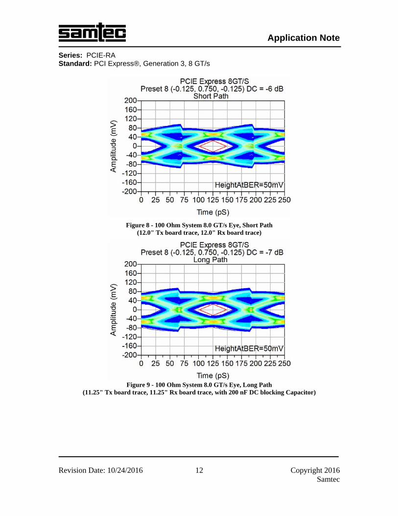
Figure 8 - 100 Ohm System 8.0 GT/s Eye, Short Path
(12.0" Tx board trace, 12.0" Rx board trace)
Figure 9 - 100 Ohm System 8.0 GT/s Eye, Long Path
(11.25" Tx board trace, 11.25" Rx board trace, with 200 nF DC blocking Capacitor)

Application Note
Series: PCIE-RA Standard: PCI Express®, Generation 3, 8 GT/s
Revision Date: 10/24/2016 13 Copyright 2016 Samtec
Figure 10 - 100 Ohm System 8.0 GT/s Eye, Short Path
(12.0" Tx board trace, 12.0" Rx board trace, with 200 nF DC blocking Capacitor)
If we set the length of the Rx adapter to 4", the maximum length for a standard PCI Express® 8.0 GT/s add-in card, we can now sweep the Tx adapter (motherboard) trace length from 1" to 30" and view the results. Figure 11 shows a plot of the measured eye heights vs. Tx trace lengths, resulting in Tx length limits of 17.5" for the long path and 20” for the short path. Figures 12, 13, 14 and 15 show the representative eyes for the 21.5” and 24” channels, with and without DC blocking capacitors. As seen previously, addition of the capacitor has a negligible impact on these long reach channels.

Application Note
Series: PCIE-RA Standard: PCI Express®, Generation 3, 8 GT/s
Revision Date: 10/24/2016 14 Copyright 2016 Samtec
Figure 11 - 100 Ohm System 8.0 GT/s Eye Height vs. Tx Length
with Rx Length = 4"
Figure 12 - 8.0 GT/s Eye, Long path
(17.5" Tx board trace, 4" Rx board trace)

Application Note
Series: PCIE-RA Standard: PCI Express®, Generation 3, 8 GT/s
Revision Date: 10/24/2016 15 Copyright 2016 Samtec
Figure 13 - 8.0 GT/s Eye, Short Path
(20" Tx board trace, 4" Rx board trace)
Figure 14 - 8.0 GT/s Eye, Long Path
(17.5" Tx board trace, 4" Rx board trace, with 200 nF DC blocking Capacitor)

Application Note
Series: PCIE-RA Standard: PCI Express®, Generation 3, 8 GT/s
Revision Date: 10/24/2016 16 Copyright 2016 Samtec
Figure 15 - 8.0 GT/s Eye, Short Path
(20" Tx board trace, 4" Rx board trace, with 200 nF DC blocking Capacitor)
Simulation sweeps with all combinations of extremely short trace segments from 0.1" to 1", were used to characterize the potential for amplitude and jitter degradation of the Tx package, Rx package and connector combination, providing a view of potential short channel low loss resonance issues. Figures 16 and 17 show the best case short channel eye openings for both the long and the short paths using Tx trace lengths of 0.3” and 0.9”, respectively; and Rx trace lengths of 0.1 for both paths. Figures 18 and 19 show the worst case, and minimally compliant short channel eye openings, for both the long and short paths using Tx trace lengths of 0.9" both paths and 0.2” and 0.1” respectively. In both cases, the equalized eye is well within compliance margins, with no serious resonance peaking issues that are beyond the capabilities of PCI Express® 8.0 GT/s equalizers.

Application Note
Series: PCIE-RA Standard: PCI Express®, Generation 3, 8 GT/s
Revision Date: 10/24/2016 17 Copyright 2016 Samtec
Figure 16 - 8.0 GT/s Eye, Long Path
(0.3" Tx board trace, 0.1" Rx board trace)
Figure 17 - 8.0 GT/s Eye, Short Path
(0.9" Tx board trace, 0.1" Rx board trace)

Application Note
Series: PCIE-RA Standard: PCI Express®, Generation 3, 8 GT/s
Revision Date: 10/24/2016 18 Copyright 2016 Samtec
Figure 18 - 8.0 GT/s Eye, Long Path
(0.9" Tx board trace, 0.2" Rx board trace)
Figure 19 - 8.0 GT/s Eye, Short Path (1.0" Tx board trace, 0.1" Rx board trace)
If we use an 85 ohm system impedance and set the length of the Rx adapter to 4", the maximum length for a standard PCI Express® 8.0 GT/s add-in card, we

Application Note
Series: PCIE-RA Standard: PCI Express®, Generation 3, 8 GT/s
Revision Date: 10/24/2016 19 Copyright 2016 Samtec
can now sweep the Tx adapter (motherboard) trace length from 1" to 30" and view the results. Figure 20 shows a plot of the measured eye heights vs. Tx trace lengths, resulting in a length limits for both the long and short paths of approximately 20" and 22.5” respectively, for our study. Figures 21 and 22 show the representative eyes for the 24" and 26.5” channels with DC blocking capacitors. Margin for an 85 ohm PCI Express® interconnect is slightly larger than that for the 100 ohm system, due to the lower loss of the 85 ohm traces using the same dielectric thickness of the 100 ohm system.
Figure 20 - 85 Ohm System 8.0 GT/s Eye Height vs. Tx Length
with Rx Length = 4"

Application Note
Series: PCIE-RA Standard: PCI Express®, Generation 3, 8 GT/s
Revision Date: 10/24/2016 20 Copyright 2016 Samtec
Figure 21 - 85 Ohm System 8.0 GT/s Eye
(20" Tx board trace, 4" Rx board trace, with 200 nF DC blocking Capacitor)
Figure 22 - 85 Ohm System 8.0 GT/s Eye
(22.5" Tx board trace, 4" Rx board trace, with 200 nF DC blocking Capacitor)

Application Note
Series: PCIE-RA Standard: PCI Express®, Generation 3, 8 GT/s
Revision Date: 10/24/2016 21 Copyright 2016 Samtec
Conclusions
A single Samtec PCIE-RA connector in a board-to-board configuration can be used in 100 ohm PCI Express® 8.0 GT/s systems with total trace lengths not to exceed 23 to 24 total inches depending on the signal path, when used with Samtec’s Final Inch™ routing, breakout, and trace width solutions as modeled and simulated in this document. 85 ohm systems have slightly higher margins and subsequently a longer reach of from 22.5 to 24 inches of total interconnect length.
Because loss is the dominant contributor to system degradation, designers should be aware that using smaller trace widths, laminates with higher loss tangent, sub optimal routing solutions with higher pair-to-pair coupling, and additional vias will decrease overall performance and the maximum allowable trace length. It is advisable, when designing systems that approach the maximum trace length limits, to perform detailed modeling, simulation, and measurement of the target design including the effects of material properties, traces, vias, and additional components.


![Skin Effects and Dielectric Loss[1]suddendocs.samtec.com/notesandwhitepapers/skin... · Title: Skin Effects and Dielectric Loss[1] Keywords Created Date: 20180220220629Z](https://static.documents.pub/doc/80x56/5f31d271bbf918721221e2d1/skin-effects-and-dielectric-loss1-title-skin-effects-and-dielectric-loss1-keywords.jpg)


![MLCC Commercial grade C series · Type: C0402 [01005 inch], C0603 [0201 inch], C1005 [0402 inch], C1608 [0603 inch], C2012 [0805 inch], C3216 [1206 inch], C3225 [1210 inch], C4532](https://static.documents.pub/doc/80x56/5f2a1b6cea53687ca900e2cc/mlcc-commercial-grade-c-series-type-c0402-01005-inch-c0603-0201-inch-c1005.jpg)


