User's GuideSLVU361B–April 2010–Revised October 2013
CPG004_DRV88xx Evaluation Modules
This document is provided as a supplement to the DRV8802, DRV8812, DRV8813, DRV8814, DRV8824,DRV8825, DRV8841 and DRV8843 datasheets. It details the hardware implementation of the CPG004DRV88xxEVM Customer Evaluation Module (EVM). On this document, DRV88xx will be usedinterchangeably to refer to any of the aforementioned devices.
1.1 Power Connectors ................................................................................................. 21.2 Test Stakes ......................................................................................................... 21.3 Jumpers ............................................................................................................. 31.4 Motor Outputs ...................................................................................................... 4
2 Installing Drivers And Software ........................................................................................... 52.1 Installing the FTDI USB Driver ................................................................................... 52.2 Installing the CPG004_DRV88xx Evaluation Board Windows Application Software ...................... 52.3 Running the Windows Application Software .................................................................... 5
3 The Windows Application .................................................................................................. 53.1 The Menu ........................................................................................................... 73.2 DRV88xx GPIO Control Signals ................................................................................. 73.3 Updating DAC Output for Current Control (VREFA and VREFB) ........................................... 83.4 DC Motor Speed Control (PWM) ................................................................................. 83.5 Operating the Stepper Motor (DRV8824) ....................................................................... 9
Where DRV88xx stands for one of DRV8812, DRV8813, DRV8814, DRV8824, DRV8825,
DRV8841 or DRV8843.
DRV8802,
Block Diagram www.ti.com
1 Block Diagram
1.1 Power ConnectorsThe DRV88xx Customer EVM offers access to VM (Motor Voltage) power rail via a terminal block (J1). Aset of test clips in parallel with the terminal block allows for the monitoring of the input power rail.
User must apply VM according to datasheet recommended parameters.
NOTE: VDD for logic and microcontroller is derived from USB interface.
1.2 Test StakesEvery pin on the DRV88xx device has been brought out to a test stake. A label on the silkscreen identifieseach signal.
For those pins that change functionality depending on device flavor, a table is provided with correspondingfunction name on its particular column.
2 CPG004_DRV88xx Evaluation Modules SLVU361B–April 2010–Revised October 2013Submit Documentation Feedback
To configure the BVREF select jumper:(a) Use position JP1-1:2 to select the respective variable resistance potentiometer.(b) Use position JP1-2:3 to select the MSP430 DAC functionality.(c) Use position JP1-5:6 to select AVREF as reference voltage source.This jumper
should not be left open as lack of a reference voltage on the device will minimizecurrent sourcing into the respective H Bridge, resulting in very poor motion orno motion at all.
(a) (b)
1 1
From Pot
From DAC
To configure the AVREF select jumper:(a) Use position JP2-1:2 to select the MSP430 DAC output (default).(b) Use position JP2-2:3 to select the respective variable resistance
potentiometer. This jumper should not be left open as lack ofreference voltage on the device will minimize current sourcinginto the respective H Bridge, resulting in very poor motion orno motion at all.
www.ti.com Block Diagram
1.3 JumpersThere are only three jumpers the user must configure as detailed below. Default configuration assumesmicrocontroller resources are being utilized. As an alternative, a variable resistance is provided on theopposing jumper configuration.
1.3.1 AVREF Select Jumper (JP2)
Figure 1. AVREF Select Jumper Configuration
1.3.2 BVREF Select Jumper (JP1)
Figure 2. BVREF Select Jumper Configuration
3SLVU361B–April 2010–Revised October 2013 CPG004_DRV88xx Evaluation ModulesSubmit Documentation Feedback
To configure the DECAY select jumper:(a) Use position JP3-1:2 to select the MSP430 GPIO functionality (default).(b) Use position JP3-2:3 to select the respective variable resistance
potentiometer. Allowing the jumper to not be placed, will result in thedevice operating under mixed decay mode.
Block Diagram www.ti.com
1.3.2.1 BVREF Default Jumper Allocation
Table 1. BVREF Default Jumper Allocation on a Per Device BasisDEVICE BVREF JUMPER DEFAULT
1.4 Motor OutputsThere are two ways of connecting the different motor styles (single bipolar stepper motor or two DCmotors) into the CPG004_DRV88xx Evaluation Module: four pin header (J4) and four position terminalblock (J3). Although feasible, we do not recommend the connection of any motor into the test clips asthese are Kelvin connections and not rated for high current output.
4 CPG004_DRV88xx Evaluation Modules SLVU361B–April 2010–Revised October 2013Submit Documentation Feedback
2.1 Installing the FTDI USB DriverInstructions on how to install the FTDI USB driver on a Windows based computer are detailed in the“USB_Drivers_Install_Readme.pdf” file supplied with the CD inside the USB_Driver folder.
2.2 Installing the CPG004_DRV88xx Evaluation Board Windows Application SoftwareCopy the contents of the “WindowsApplication” folder provided within the CD, into your hard disk.
2.3 Running the Windows Application SoftwareTo run the application, double click the CPG004_DRV88xxEVM_R0p2.exe application icon found on thesame folder the application was extracted into.
3 The Windows ApplicationThe CPG004_DRV88xxEVM Windows application is the software counterpart for the CPG004_DRV88xxEVM. It allows the PC computer to connect to the MSP430F1612 microcontroller though an USB interfacechip. Once connection is established and commands are sent, microcontroller takes care of configuringcontrol signals and administering certain levels of automation, such as microstepping generation for(DRV8812/13), STEP and DIR control (for DRV8824/25) or PWM output (for DRV8812/13/14/41/43).
The graphical user interface (GUI) has been designed to allow for all of the DRV88xx device’s functionalityto be tested without having to intervene with the hardware, except for the proper configuration of jumpers,when needed.
The following pictures show the CPG004_DRV88xxEVM_R1p1.exe main screen. The application isdivided into three tabs: one for each one of the three available device flavors. The menu contains items toconfigure and enable/disable the serial port.
Figure 4. DRV8802-12-13-14 Tab
The DRV8802-12-13-14 tab contains all the control signals needed to control motor enablement (ENABLEA, ENABLE B), direction of rotation (PHASE A, PHASE B) and current control (AIx and BIx). Access toboth DAC generating VREF analog voltages is achieved by moving sliders. Another set of sliders allow thecontrol of PWM duty cycle on ENABLE x pins. This is intended for motion control.
A simple stepper demo allows hooking a bipolar stepper to the DRV8812 EVM and have its speed anddirection controlled by an algorithm which modulates the VREF current in a high resolution microsteppingstyle. This function is achieved by using both MSP430 DAC outputs and is only available if respectivejumpers are set for dual DAC connection (as default).
5SLVU361B–April 2010–Revised October 2013 CPG004_DRV88xx Evaluation ModulesSubmit Documentation Feedback
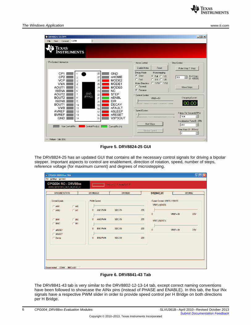
The DRV8824-25 has an updated GUI that contains all the necessary control signals for driving a bipolarstepper. Important aspects to control are enablement, direction of rotation, speed, number of steps,reference voltage (for maximum current) and degrees of microstepping.
Figure 6. DRV8841-43 Tab
The DRV8841-43 tab is very similar to the DRV8802-12-13-14 tab, except correct naming conventionshave been followed to showcase the AINx pins (instead of PHASE and ENABLE). In this tab, the four INxsignals have a respective PWM slider in order to provide speed control per H Bridge on both directionsper H Bridge.
6 CPG004_DRV88xx Evaluation Modules SLVU361B–April 2010–Revised October 2013Submit Documentation Feedback
3.1 The MenuThe menu at the top of the application offers a series of quick options for how the COM port is to behave.
File: Exit – Terminates the application
Settings: Port – Selects from COM1 to COM4. Default is COM4.
The serial port's actual port number defaults to what we have specified on the“USB_Drivers_Install_Readme.pdf”. However, any port between COM 1 and COM 4 are equally usable.
Connect: Opens the serial port. When this menu item is pressed, its caption changes to “Disconnect”.
Disconnect: Closes the serial port. When this menu item is pressed, its caption changes to “Connect”.
After opening the application, the order of events should be:1. Go to Settings → Port and choose the COM Port where the FTDI device has been configured to work.
If the COM port is 4, then this step can be skipped, as application defaults to COM4.2. Press Connect. If the port is available, the menu changes the “Connect“ caption to “Disconnect“. Press
Disconnect to disable the serial communications.3. <1><0><0> should return on the text box as an acknowledge. The text box also changes from red to
green.4. The application is ready for use.
3.2 DRV88xx GPIO Control SignalsOnce the application is communicating with the interface board, the control signals can be actuated bychecking or un-checking check boxes on the Signals frame. Each tab will have a different set of controlsignals as depending on the device being interface on. nSLEEP and nRESET control signals will be on alltabs.
Functionality of control signals is identical across the platform. A checked checkbox translates to a HI levelon the respective control signal. Unchecked checkboxes translates to a LO level on the respective controlsignals.
Figure 7. GPIO Control Signals
3.2.1 About DECAYThe DECAY pin is in reality a triple state input. The GPIO operates as HI and LO according to thecheckbox. To have the DECAY pin floating, engaging mixed decay mode, simply remove the decayjumper JP3.
7SLVU361B–April 2010–Revised October 2013 CPG004_DRV88xx Evaluation ModulesSubmit Documentation Feedback
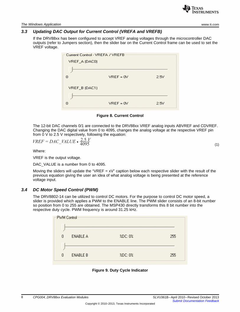
3.3 Updating DAC Output for Current Control (VREFA and VREFB)If the DRV88xx has been configured to accept VREF analog voltages through the microcontroller DACoutputs (refer to Jumpers section), then the slider bar on the Current Control frame can be used to set theVREF voltage.
Figure 8. Current Control
The 12-bit DAC channels 0/1 are connected to the DRV88xx VREF analog inputs ABVREF and CDVREF.Changing the DAC digital value from 0 to 4095, changes the analog voltage at the respective VREF pinfrom 0 V to 2.5 V respectively, following the equation:
(1)
Where:
VREF is the output voltage.
DAC_VALUE is a number from 0 to 4095.
Moving the sliders will update the “VREF = xV” caption below each respective slider with the result of theprevious equation giving the user an idea of what analog voltage is being presented at the referencevoltage input.
3.4 DC Motor Speed Control (PWM)The DRV8802-14 can be utilized to control DC motors. For the purpose to control DC motor speed, aslider is provided which applies a PWM to the ENABLE line. The PWM slider consists of an 8-bit numberso position from 0 to 255 are obtained. The MSP430 directly transforms this 8 bit number into therespective duty cycle. PWM frequency is around 31.25 kHz.
Figure 9. Duty Cycle Indicator
8 CPG004_DRV88xx Evaluation Modules SLVU361B–April 2010–Revised October 2013Submit Documentation Feedback
When the slider bar is moved across, the Duty Cycle indicator is updated accordingly. Resulting duty cycleis an integer number between 0 and 100 and it is computed according to the equation:
(2)
The DRV8841-43 will offer the same ability to apply a PWM signal to each one of the INx pins.
Figure 10. PWM Signal on INx Pins
3.5 Operating the Stepper Motor (DRV8824)
3.5.1 Turning the Stepper MotorThe Windows application, in conjunction with the MSP430F1612 microcontroller, utilizes a series of timersto coordinate the rate of steps sent to the device. Once all the control signals are configured accordingly,(ENABLEn = LO, SLEEPn = HI, RESETn = HI; DIR, USMx can be HI or LO depending on preferred modeof operation), the motor is ready to be turned.
The DRV88xx EVM allows for the possibility of coordinating step rates such that accelerating anddecelerating profiles are achieved. Both acceleration and deceleration are controlled by the sameparameters, acceleration rate and time base.
When the motor starts, it always starts at the slowed PPS speed (62 pulses per second). The controllerwill accelerate the motor in order to reach the PPS speed. Acceleration rate is an 8-bit number (0 to 255)that gets added to the current PPS speed and time base is an 8-bit number (0 to 255) that specifies howmany milliseconds will elapse from one speed increase to the next. Once the specified PPS speed hasbeen achieved, the acceleration stops.
When the motor stops, the inverse of the above description occurs.
9SLVU361B–April 2010–Revised October 2013 CPG004_DRV88xx Evaluation ModulesSubmit Documentation Feedback
The Windows application frame to control speed, acceleration and deceleration, as well as motor start andstop, is shown in Figure 12.
Figure 12. Speed Control
Pressing the “Start Steps” button, will start the timer and pulses will be generated at the rate specified bythe decimal number at the PPS text box. Once the “Start Steps” button is pressed it becomes the“Stepping” button. Press the “Stepping” button to stop the stepper motion.
When the motor is stepping, the “Update Speed” button becomes enabled. Speed can be updated bymodifying the PPS text box and then pressing the “Update Speed” button. The “Speed Button is disabledevery time the motor is not turning because the stepping has been halted by pressing the “Stepping”button.
3.5.2 Step by Step ControlThe step control frame has a series of tools to control the stepping of the motor on a predeterminednumber of steps fashion.
The “Pulse Step” button allows for a single step to be issued. Remember that a STEP takes place whenSTEP goes from LO to HI.
10 CPG004_DRV88xx Evaluation Modules SLVU361B–April 2010–Revised October 2013Submit Documentation Feedback
To move the motor a number of steps and then stop, fill the # of Steps text box with a decimal numberfrom 0 to 65535 and the motor will move that number of steps at the speed specified on the PPS text box.No acceleration or deceleration takes place under this function.
3.5.3 Stepper Speed CalculatorIn order to easily translate steps per second to actual angular velocity, a simple calculator is provided. Thecalculator extracts step resolution information from the Mode x pins values and STEP frequency from thePPS text box. The user must then provide number of steps per resolution the motor has beenmanufactured to achieve. For example, a 1.8 degrees stepper motor would have 200 steps per revolution,and so on.
By pressing the Compute button, the calculator reports the revolutions per second and revolutions perminute parameters. For example, on the picture below, the stepping rate was set to 4000 steps persecond. While microstepping with 4 degrees of microstepping, a motor with 200 steps per revolutionshould be moving at 5 revolutions per second or 300 revolutions per minute.
Figure 14. Stepper Speed Calculator
11SLVU361B–April 2010–Revised October 2013 CPG004_DRV88xx Evaluation ModulesSubmit Documentation Feedback
Changes from A Revision (June, 2011) to B Revision ................................................................................................... Page
• Changed figure 5 and supporting text below image ................................................................................. 6
NOTE: Page numbers for previous revisions may differ from page numbers in the current version.
16 Revision History SLVU361B–April 2010–Revised October 2013Submit Documentation Feedback
Texas Instruments (TI) provides the enclosed Evaluation Board/Kit/Module (EVM) under the following conditions:
The user assumes all responsibility and liability for proper and safe handling of the goods. Further, the user indemnifies TI from all claimsarising from the handling or use of the goods.
Should this evaluation board/kit not meet the specifications indicated in the User’s Guide, the board/kit may be returned within 30 days fromthe date of delivery for a full refund. THE FOREGOING LIMITED WARRANTY IS THE EXCLUSIVE WARRANTY MADE BY SELLER TOBUYER AND IS IN LIEU OF ALL OTHER WARRANTIES, EXPRESSED, IMPLIED, OR STATUTORY, INCLUDING ANY WARRANTY OFMERCHANTABILITY OR FITNESS FOR ANY PARTICULAR PURPOSE. EXCEPT TO THE EXTENT OF THE INDEMNITY SET FORTHABOVE, NEITHER PARTY SHALL BE LIABLE TO THE OTHER FOR ANY INDIRECT, SPECIAL, INCIDENTAL, OR CONSEQUENTIALDAMAGES.
Please read the User's Guide and, specifically, the Warnings and Restrictions notice in the User's Guide prior to handling the product. Thisnotice contains important safety information about temperatures and voltages. For additional information on TI's environmental and/or safetyprograms, please visit www.ti.com/esh or contact TI.
No license is granted under any patent right or other intellectual property right of TI covering or relating to any machine, process, orcombination in which such TI products or services might be or are used. TI currently deals with a variety of customers for products, andtherefore our arrangement with the user is not exclusive. TI assumes no liability for applications assistance, customer product design,software performance, or infringement of patents or services described herein.
REGULATORY COMPLIANCE INFORMATION
As noted in the EVM User’s Guide and/or EVM itself, this EVM and/or accompanying hardware may or may not be subject to the FederalCommunications Commission (FCC) and Industry Canada (IC) rules.
For EVMs not subject to the above rules, this evaluation board/kit/module is intended for use for ENGINEERING DEVELOPMENT,DEMONSTRATION OR EVALUATION PURPOSES ONLY and is not considered by TI to be a finished end product fit for general consumeruse. It generates, uses, and can radiate radio frequency energy and has not been tested for compliance with the limits of computingdevices pursuant to part 15 of FCC or ICES-003 rules, which are designed to provide reasonable protection against radio frequencyinterference. Operation of the equipment may cause interference with radio communications, in which case the user at his own expense willbe required to take whatever measures may be required to correct this interference.
General Statement for EVMs including a radio
User Power/Frequency Use Obligations: This radio is intended for development/professional use only in legally allocated frequency andpower limits. Any use of radio frequencies and/or power availability of this EVM and its development application(s) must comply with locallaws governing radio spectrum allocation and power limits for this evaluation module. It is the user’s sole responsibility to only operate thisradio in legally acceptable frequency space and within legally mandated power limitations. Any exceptions to this are strictly prohibited andunauthorized by Texas Instruments unless user has obtained appropriate experimental/development licenses from local regulatoryauthorities, which is responsibility of user including its acceptable authorization.
For EVMs annotated as FCC – FEDERAL COMMUNICATIONS COMMISSION Part 15 Compliant
Caution
This device complies with part 15 of the FCC Rules. Operation is subject to the following two conditions: (1) This device may not causeharmful interference, and (2) this device must accept any interference received, including interference that may cause undesired operation.
Changes or modifications not expressly approved by the party responsible for compliance could void the user's authority to operate theequipment.
FCC Interference Statement for Class A EVM devices
This equipment has been tested and found to comply with the limits for a Class A digital device, pursuant to part 15 of the FCC Rules.These limits are designed to provide reasonable protection against harmful interference when the equipment is operated in a commercialenvironment. This equipment generates, uses, and can radiate radio frequency energy and, if not installed and used in accordance with theinstruction manual, may cause harmful interference to radio communications. Operation of this equipment in a residential area is likely tocause harmful interference in which case the user will be required to correct the interference at his own expense.
FCC Interference Statement for Class B EVM devices
This equipment has been tested and found to comply with the limits for a Class B digital device, pursuant to part 15 of the FCC Rules.These limits are designed to provide reasonable protection against harmful interference in a residential installation. This equipmentgenerates, uses and can radiate radio frequency energy and, if not installed and used in accordance with the instructions, may causeharmful interference to radio communications. However, there is no guarantee that interference will not occur in a particular installation. Ifthis equipment does cause harmful interference to radio or television reception, which can be determined by turning the equipment off andon, the user is encouraged to try to correct the interference by one or more of the following measures:
• Reorient or relocate the receiving antenna.• Increase the separation between the equipment and receiver.• Connect the equipment into an outlet on a circuit different from that to which the receiver is connected.• Consult the dealer or an experienced radio/TV technician for help.
For EVMs annotated as IC – INDUSTRY CANADA Compliant
This Class A or B digital apparatus complies with Canadian ICES-003.
Changes or modifications not expressly approved by the party responsible for compliance could void the user’s authority to operate theequipment.
Concerning EVMs including radio transmitters
This device complies with Industry Canada licence-exempt RSS standard(s). Operation is subject to the following two conditions: (1) thisdevice may not cause interference, and (2) this device must accept any interference, including interference that may cause undesiredoperation of the device.
Concerning EVMs including detachable antennas
Under Industry Canada regulations, this radio transmitter may only operate using an antenna of a type and maximum (or lesser) gainapproved for the transmitter by Industry Canada. To reduce potential radio interference to other users, the antenna type and its gain shouldbe so chosen that the equivalent isotropically radiated power (e.i.r.p.) is not more than that necessary for successful communication.
This radio transmitter has been approved by Industry Canada to operate with the antenna types listed in the user guide with the maximumpermissible gain and required antenna impedance for each antenna type indicated. Antenna types not included in this list, having a gaingreater than the maximum gain indicated for that type, are strictly prohibited for use with this device.
Cet appareil numérique de la classe A ou B est conforme à la norme NMB-003 du Canada.
Les changements ou les modifications pas expressément approuvés par la partie responsable de la conformité ont pu vider l’autorité del'utilisateur pour actionner l'équipement.
Concernant les EVMs avec appareils radio
Le présent appareil est conforme aux CNR d'Industrie Canada applicables aux appareils radio exempts de licence. L'exploitation estautorisée aux deux conditions suivantes : (1) l'appareil ne doit pas produire de brouillage, et (2) l'utilisateur de l'appareil doit accepter toutbrouillage radioélectrique subi, même si le brouillage est susceptible d'en compromettre le fonctionnement.
Concernant les EVMs avec antennes détachables
Conformément à la réglementation d'Industrie Canada, le présent émetteur radio peut fonctionner avec une antenne d'un type et d'un gainmaximal (ou inférieur) approuvé pour l'émetteur par Industrie Canada. Dans le but de réduire les risques de brouillage radioélectrique àl'intention des autres utilisateurs, il faut choisir le type d'antenne et son gain de sorte que la puissance isotrope rayonnée équivalente(p.i.r.e.) ne dépasse pas l'intensité nécessaire à l'établissement d'une communication satisfaisante.
Le présent émetteur radio a été approuvé par Industrie Canada pour fonctionner avec les types d'antenne énumérés dans le manueld’usage et ayant un gain admissible maximal et l'impédance requise pour chaque type d'antenne. Les types d'antenne non inclus danscette liste, ou dont le gain est supérieur au gain maximal indiqué, sont strictement interdits pour l'exploitation de l'émetteur.
SPACER
SPACER
SPACER
SPACER
SPACER
SPACER
SPACER
SPACER
【【Important Notice for Users of EVMs for RF Products in Japan】】This development kit is NOT certified as Confirming to Technical Regulations of Radio Law of Japan
If you use this product in Japan, you are required by Radio Law of Japan to follow the instructions below with respect to this product:
1. Use this product in a shielded room or any other test facility as defined in the notification #173 issued by Ministry of Internal Affairs andCommunications on March 28, 2006, based on Sub-section 1.1 of Article 6 of the Ministry’s Rule for Enforcement of Radio Law ofJapan,
2. Use this product only after you obtained the license of Test Radio Station as provided in Radio Law of Japan with respect to thisproduct, or
3. Use of this product only after you obtained the Technical Regulations Conformity Certification as provided in Radio Law of Japan withrespect to this product. Also, please do not transfer this product, unless you give the same notice above to the transferee. Please notethat if you could not follow the instructions above, you will be subject to penalties of Radio Law of Japan.
Texas Instruments Japan Limited(address) 24-1, Nishi-Shinjuku 6 chome, Shinjuku-ku, Tokyo, Japan
EVALUATION BOARD/KIT/MODULE (EVM)WARNINGS, RESTRICTIONS AND DISCLAIMERS
For Feasibility Evaluation Only, in Laboratory/Development Environments. Unless otherwise indicated, this EVM is not a finishedelectrical equipment and not intended for consumer use. It is intended solely for use for preliminary feasibility evaluation inlaboratory/development environments by technically qualified electronics experts who are familiar with the dangers and application risksassociated with handling electrical mechanical components, systems and subsystems. It should not be used as all or part of a finished endproduct.
Your Sole Responsibility and Risk. You acknowledge, represent and agree that:
1. You have unique knowledge concerning Federal, State and local regulatory requirements (including but not limited to Food and DrugAdministration regulations, if applicable) which relate to your products and which relate to your use (and/or that of your employees,affiliates, contractors or designees) of the EVM for evaluation, testing and other purposes.
2. You have full and exclusive responsibility to assure the safety and compliance of your products with all such laws and other applicableregulatory requirements, and also to assure the safety of any activities to be conducted by you and/or your employees, affiliates,contractors or designees, using the EVM. Further, you are responsible to assure that any interfaces (electronic and/or mechanical)between the EVM and any human body are designed with suitable isolation and means to safely limit accessible leakage currents tominimize the risk of electrical shock hazard.
3. Since the EVM is not a completed product, it may not meet all applicable regulatory and safety compliance standards (such as UL,CSA, VDE, CE, RoHS and WEEE) which may normally be associated with similar items. You assume full responsibility to determineand/or assure compliance with any such standards and related certifications as may be applicable. You will employ reasonablesafeguards to ensure that your use of the EVM will not result in any property damage, injury or death, even if the EVM should fail toperform as described or expected.
4. You will take care of proper disposal and recycling of the EVM’s electronic components and packing materials.
Certain Instructions. It is important to operate this EVM within TI’s recommended specifications and environmental considerations per theuser guidelines. Exceeding the specified EVM ratings (including but not limited to input and output voltage, current, power, andenvironmental ranges) may cause property damage, personal injury or death. If there are questions concerning these ratings please contacta TI field representative prior to connecting interface electronics including input power and intended loads. Any loads applied outside of thespecified output range may result in unintended and/or inaccurate operation and/or possible permanent damage to the EVM and/orinterface electronics. Please consult the EVM User's Guide prior to connecting any load to the EVM output. If there is uncertainty as to theload specification, please contact a TI field representative. During normal operation, some circuit components may have case temperaturesgreater than 60°C as long as the input and output are maintained at a normal ambient operating temperature. These components includebut are not limited to linear regulators, switching transistors, pass transistors, and current sense resistors which can be identified using theEVM schematic located in the EVM User's Guide. When placing measurement probes near these devices during normal operation, pleasebe aware that these devices may be very warm to the touch. As with all electronic evaluation tools, only qualified personnel knowledgeablein electronic measurement and diagnostics normally found in development environments should use these EVMs.
Agreement to Defend, Indemnify and Hold Harmless. You agree to defend, indemnify and hold TI, its licensors and their representativesharmless from and against any and all claims, damages, losses, expenses, costs and liabilities (collectively, "Claims") arising out of or inconnection with any use of the EVM that is not in accordance with the terms of the agreement. This obligation shall apply whether Claimsarise under law of tort or contract or any other legal theory, and even if the EVM fails to perform as described or expected.
Safety-Critical or Life-Critical Applications. If you intend to evaluate the components for possible use in safety critical applications (suchas life support) where a failure of the TI product would reasonably be expected to cause severe personal injury or death, such as deviceswhich are classified as FDA Class III or similar classification, then you must specifically notify TI of such intent and enter into a separateAssurance and Indemnity Agreement.
IMPORTANT NOTICE FOR TI REFERENCE DESIGNSTexas Instruments Incorporated ("TI") reference designs are solely intended to assist designers (“Buyers”) who are developing systems thatincorporate TI semiconductor products (also referred to herein as “components”). Buyer understands and agrees that Buyer remainsresponsible for using its independent analysis, evaluation and judgment in designing Buyer’s systems and products.TI reference designs have been created using standard laboratory conditions and engineering practices. TI has not conducted anytesting other than that specifically described in the published documentation for a particular reference design. TI may makecorrections, enhancements, improvements and other changes to its reference designs.Buyers are authorized to use TI reference designs with the TI component(s) identified in each particular reference design and to modify thereference design in the development of their end products. HOWEVER, NO OTHER LICENSE, EXPRESS OR IMPLIED, BY ESTOPPELOR OTHERWISE TO ANY OTHER TI INTELLECTUAL PROPERTY RIGHT, AND NO LICENSE TO ANY THIRD PARTY TECHNOLOGYOR INTELLECTUAL PROPERTY RIGHT, IS GRANTED HEREIN, including but not limited to any patent right, copyright, mask work right,or other intellectual property right relating to any combination, machine, or process in which TI components or services are used.Information published by TI regarding third-party products or services does not constitute a license to use such products or services, or awarranty or endorsement thereof. Use of such information may require a license from a third party under the patents or other intellectualproperty of the third party, or a license from TI under the patents or other intellectual property of TI.TI REFERENCE DESIGNS ARE PROVIDED "AS IS". TI MAKES NO WARRANTIES OR REPRESENTATIONS WITH REGARD TO THEREFERENCE DESIGNS OR USE OF THE REFERENCE DESIGNS, EXPRESS, IMPLIED OR STATUTORY, INCLUDING ACCURACY ORCOMPLETENESS. TI DISCLAIMS ANY WARRANTY OF TITLE AND ANY IMPLIED WARRANTIES OF MERCHANTABILITY, FITNESSFOR A PARTICULAR PURPOSE, QUIET ENJOYMENT, QUIET POSSESSION, AND NON-INFRINGEMENT OF ANY THIRD PARTYINTELLECTUAL PROPERTY RIGHTS WITH REGARD TO TI REFERENCE DESIGNS OR USE THEREOF. TI SHALL NOT BE LIABLEFOR AND SHALL NOT DEFEND OR INDEMNIFY BUYERS AGAINST ANY THIRD PARTY INFRINGEMENT CLAIM THAT RELATES TOOR IS BASED ON A COMBINATION OF COMPONENTS PROVIDED IN A TI REFERENCE DESIGN. IN NO EVENT SHALL TI BELIABLE FOR ANY ACTUAL, SPECIAL, INCIDENTAL, CONSEQUENTIAL OR INDIRECT DAMAGES, HOWEVER CAUSED, ON ANYTHEORY OF LIABILITY AND WHETHER OR NOT TI HAS BEEN ADVISED OF THE POSSIBILITY OF SUCH DAMAGES, ARISING INANY WAY OUT OF TI REFERENCE DESIGNS OR BUYER’S USE OF TI REFERENCE DESIGNS.TI reserves the right to make corrections, enhancements, improvements and other changes to its semiconductor products and services perJESD46, latest issue, and to discontinue any product or service per JESD48, latest issue. Buyers should obtain the latest relevantinformation before placing orders and should verify that such information is current and complete. All semiconductor products are soldsubject to TI’s terms and conditions of sale supplied at the time of order acknowledgment.TI warrants performance of its components to the specifications applicable at the time of sale, in accordance with the warranty in TI’s termsand conditions of sale of semiconductor products. Testing and other quality control techniques for TI components are used to the extent TIdeems necessary to support this warranty. Except where mandated by applicable law, testing of all parameters of each component is notnecessarily performed.TI assumes no liability for applications assistance or the design of Buyers’ products. Buyers are responsible for their products andapplications using TI components. To minimize the risks associated with Buyers’ products and applications, Buyers should provideadequate design and operating safeguards.Reproduction of significant portions of TI information in TI data books, data sheets or reference designs is permissible only if reproduction iswithout alteration and is accompanied by all associated warranties, conditions, limitations, and notices. TI is not responsible or liable forsuch altered documentation. Information of third parties may be subject to additional restrictions.Buyer acknowledges and agrees that it is solely responsible for compliance with all legal, regulatory and safety-related requirementsconcerning its products, and any use of TI components in its applications, notwithstanding any applications-related information or supportthat may be provided by TI. Buyer represents and agrees that it has all the necessary expertise to create and implement safeguards thatanticipate dangerous failures, monitor failures and their consequences, lessen the likelihood of dangerous failures and take appropriateremedial actions. Buyer will fully indemnify TI and its representatives against any damages arising out of the use of any TI components inBuyer’s safety-critical applications.In some cases, TI components may be promoted specifically to facilitate safety-related applications. With such components, TI’s goal is tohelp enable customers to design and create their own end-product solutions that meet applicable functional safety standards andrequirements. Nonetheless, such components are subject to these terms.No TI components are authorized for use in FDA Class III (or similar life-critical medical equipment) unless authorized officers of the partieshave executed an agreement specifically governing such use.Only those TI components that TI has specifically designated as military grade or “enhanced plastic” are designed and intended for use inmilitary/aerospace applications or environments. Buyer acknowledges and agrees that any military or aerospace use of TI components thathave not been so designated is solely at Buyer's risk, and Buyer is solely responsible for compliance with all legal and regulatoryrequirements in connection with such use.TI has specifically designated certain components as meeting ISO/TS16949 requirements, mainly for automotive use. In any case of use ofnon-designated products, TI will not be responsible for any failure to meet ISO/TS16949.