33
CX28331/2/3-1x Evaluation Module User Guide 28333-EVMD-010-B February 2003
| Date post: | 08-Mar-2018 |
| Category: |
Documents |
| Upload: | trinhkhanh |
| View: | 216 times |
| Download: | 4 times |

CX28331/2/3-1x Evaluation Module User Guide
28333-EVMD-010-BFebruary 2003

© 2002, 2003 Mindspeed Technologies™, a Conexant BusinessAll Rights Reserved.
Information in this document is provided in connection with Mindspeed Technologies (“Mindspeed”) products. These materials are provided by Mindspeed as a service to its customers and may be used for informational purposes only. Mindspeed assumes no responsibility for errors or omissions in these materials. Mindspeed may make changes to specifications and product descriptions at any time, without notice. Mindspeed makes no commitment to update the information and shall have no responsibility whatsoever for conflicts or incompatibilities arising from future changes to its specifications and product descriptions.
No license, express or implied, by estoppel or otherwise, to any intellectual property rights is granted by this document. Except as provided in Mindspeed’s Terms and Conditions of Sale for such products, Mindspeed assumes no liability whatsoever.
THESE MATERIALS ARE PROVIDED “AS IS” WITHOUT WARRANTY OF ANY KIND, EITHER EXPRESS OR IMPLIED, RELATING TO SALE AND/OR USE OF MINDSPEED PRODUCTS INCLUDING LIABILITY OR WARRANTIES RELATING TO FITNESS FOR A PARTICULAR PURPOSE, CONSEQUENTIAL OR INCIDENTAL DAMAGES, MERCHANTABILITY, OR INFRINGEMENT OF ANY PATENT, COPYRIGHT OR OTHER INTELLECTUAL PROPERTY RIGHT. MINDSPEED FURTHER DOES NOT WARRANT THE ACCURACY OR COMPLETENESS OF THE INFORMATION, TEXT, GRAPHICS OR OTHER ITEMS CONTAINED WITHIN THESE MATERIALS. MINDSPEED SHALL NOT BE LIABLE FOR ANY SPECIAL, INDIRECT, INCIDENTAL, OR CONSEQUENTIAL DAMAGES, INCLUDING WITHOUT LIMITATION, LOST REVENUES OR LOST PROFITS, WHICH MAY RESULT FROM THE USE OF THESE MATERIALS.
Mindspeed products are not intended for use in medical, lifesaving or life sustaining applications. Mindspeed customers using or selling Mindspeed products for use in such applications do so at their own risk and agree to fully indemnify Mindspeed for any damages resulting from such improper use or sale.
The following are trademarks of Conexant Systems, Inc.: Mindspeed Technologies™, the Mindspeed™ logo, and “Build It First”™. Product names or services listed in this publication are for identification purposes only, and may be trademarks of third parties. Third-party brands and names are the property of their respective owners. For additional disclaimer information, please consult Mindspeed Technologies Legal Information posted at www.mindspeed.com which is incorporated by reference.
28333-EVMD-010-B Mindspeed Technologies™
See page iii for a listing of kit configurations.
Ordering Information EVM Board Model Number Order Number
CX28331/2/3–1x Evaluation Module BT01-D300-002
Revision HistoryRevision Level Date Description
A — September 1999 Initial release.
B — February 2003 Changed CN8332/CN8333 EVM Users Guide (Doc # N8333UG1B) to CX28331/2/3-1x EVM Users Guide

iii Mindspeed Technologies™ 28333-EVMD-010-B
CX28331/2/3-1x EVM User Guide
CX28331/2/3-1x EVM Kit Contents
Quantity Description Order Number
1 CX28331/2/3-1x EVM board (DS3 default) BT01-D300-002
1 CX28331/2/3-1x EVM Users Guide 28333-EVMD-010-B
1 CX28331/2/3-1x Data Sheet 2833X-DSH-001
3 Crystals (44.736 (installed), 34.368, 51.840 MHz
4 Jumpers (Mini)

28333-EVMD-010-B Mindspeed Technologies™ iv
CX28331/2/3-1x EVM User Guide
Contents
Contents . . . . . . . . . . . . . . . . . . . . . . . . . . . . . . . . . . . . . . . . . . . . . . . . . . . . . . . . . v
Figures . . . . . . . . . . . . . . . . . . . . . . . . . . . . . . . . . . . . . . . . . . . . . . . . . . . . . . . . vii
Tables . . . . . . . . . . . . . . . . . . . . . . . . . . . . . . . . . . . . . . . . . . . . . . . . . . . . . . . . . ix
1.0 CX28331/2/3–1x Evaluation Module . . . . . . . . . . . . . . . . . . . . . . . . . . . . . . . . . . 1-11.1 Evaluation Module Features. . . . . . . . . . . . . . . . . . . . . . . . . . . . . . . . . . . . . . . . . . . . . . . . . . . . . . . . . 1-11.2 Introduction. . . . . . . . . . . . . . . . . . . . . . . . . . . . . . . . . . . . . . . . . . . . . . . . . . . . . . . . . . . . . . . . . . . . . 1-1
2.0 Setting Up the CX28331/2/3–1x EVM . . . . . . . . . . . . . . . . . . . . . . . . . . . . . . . . . . 2-1
3.0 Jumper and Switch Connections . . . . . . . . . . . . . . . . . . . . . . . . . . . . . . . . . . . . . 3-13.1 Jumper Connections . . . . . . . . . . . . . . . . . . . . . . . . . . . . . . . . . . . . . . . . . . . . . . . . . . . . . . . . . . . . . . 3-13.2 Items Not in Final Design. . . . . . . . . . . . . . . . . . . . . . . . . . . . . . . . . . . . . . . . . . . . . . . . . . . . . . . . . . . 3-1
4.0 Schematics, Silkscreen and Board Layout . . . . . . . . . . . . . . . . . . . . . . . . . . . . . . 4-1
5.0 Parts Specifications and Dimensions . . . . . . . . . . . . . . . . . . . . . . . . . . . . . . . . . 5-15.1 Suggested Vendor Information . . . . . . . . . . . . . . . . . . . . . . . . . . . . . . . . . . . . . . . . . . . . . . . . . . . . . . 5-1
6.0 Technical Support and Documentation . . . . . . . . . . . . . . . . . . . . . . . . . . . . . . . . 6-1
28333-EVMD-010-B Mindspeed Technologies™ v

Contents CX28331/2/3-1x EVM User Guide
vi Mindspeed Technologies™ 28333-EVMD-010-B l

Figures
Figure 1-1. Picture of CX28331/2/3-1x EVM . . . . . . . . . . . . . . . . . . . . . . . . . . . . . . . . . . . . . . . . . . . . . 1-2Figure 2-1. DIP Switch Settings . . . . . . . . . . . . . . . . . . . . . . . . . . . . . . . . . . . . . . . . . . . . . . . . . . . . . . 2-1Figure 4-1. CX28331/2/3-1x Evaluation Module . . . . . . . . . . . . . . . . . . . . . . . . . . . . . . . . . . . . . . . . . . 4-2Figure 4-2. CX28331/2/3-1x Evaluation Module—Layer 1 . . . . . . . . . . . . . . . . . . . . . . . . . . . . . . . . . . 4-3Figure 4-3. CX28331/2/3-1x Evaluation Module—Layer 2 . . . . . . . . . . . . . . . . . . . . . . . . . . . . . . . . . . 4-4Figure 4-4. CX28331/2/3-1x Evaluation Module—Layer 3 . . . . . . . . . . . . . . . . . . . . . . . . . . . . . . . . . . 4-5Figure 4-5. CX28331/2/3-1x Evaluation Module—Layer 4 . . . . . . . . . . . . . . . . . . . . . . . . . . . . . . . . . . 4-6Figure 4-6. CX28331/2/3-1x Evaluation Module—Bottom Side . . . . . . . . . . . . . . . . . . . . . . . . . . . . . . . 4-7Figure 4-7. CX28331/2/3-1x Evaluation Module—Schematic #1 . . . . . . . . . . . . . . . . . . . . . . . . . . . . . . 4-8Figure 4-8. CX28331/2/3-1x Evaluation Module—Schematic #2 . . . . . . . . . . . . . . . . . . . . . . . . . . . . . . 4-9
28333-EVMD-010-B Mindspeed Technologies™ vii

Figures CX28331/2/3-1x EVM User Guide
viii Mindspeed Technologies™ 28333-EVMD-010-B

Tables
Table 2-1. Crystal Oscillator Values. . . . . . . . . . . . . . . . . . . . . . . . . . . . . . . . . . . . . . . . . . . . . . . . . . . . 2-1Table 2-2. SW1, SW2, and SW3 Settings . . . . . . . . . . . . . . . . . . . . . . . . . . . . . . . . . . . . . . . . . . . . . . . 2-2Table 2-3. SW4 Setting . . . . . . . . . . . . . . . . . . . . . . . . . . . . . . . . . . . . . . . . . . . . . . . . . . . . . . . . . . . . . 2-2Table 2-4. RLOS Indicators. . . . . . . . . . . . . . . . . . . . . . . . . . . . . . . . . . . . . . . . . . . . . . . . . . . . . . . . . . 2-3Table 2-5. Connector J11 Digital Rail/NRZ Data Signals . . . . . . . . . . . . . . . . . . . . . . . . . . . . . . . . . . . . 2-4
28333-EVMD-010-B Mindspeed Technologies™ ix

Tables CX28331/2/3-1x EVM User Guide
x Mindspeed Technologies™ 28333-EVMD-010-B

28333-EVMD-010-B
1.0 CX28331/2/3–1x Evaluation Module
1.1 Evaluation Module Features
! Allows complete evaluation of the CX28331/2/3–1x (DS3/E3/STS-1 LIU) devices! Device operation settings via DIP switches and jumpers, no microprocessor
needed for the Line Interface Unit (LIU)! Receive Loss of Signal (RLOS) performance monitoring indicators via LEDs! Jumper connectors for easy access to signals.
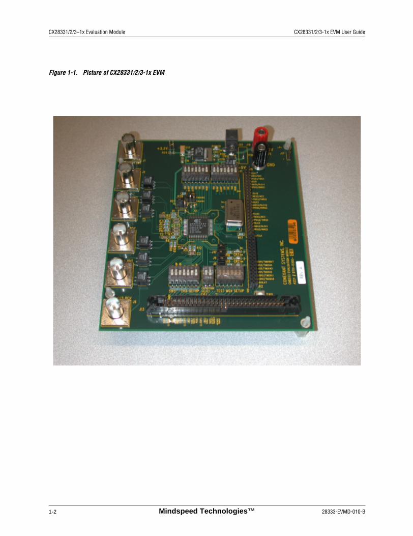
1.2 IntroductionThis User Guide describes the physical layout, important features, and a step-by-step procedure on the setup and use of the CX28331/2/3–1x test and Evaluation Module (EVM). The CX28331/2/3–1x EVM is a demonstration and test platform for Mindspeed’s family of Line Interface Units (LIUs). The CX28331/2/3–1x is available as a single, dual, or triple channel DS3/E3/STS-1 fully-integrated LIU. Each channel of the LIU can be independently configured via DIP switches to select various modes and test operations. This EVM platform allows system developers and product designers to quickly test and evaluate the functionality and performance of the CX28331/2/3–1x device.
The EVM board consists of a soldered CX28331/2/3–1x with peripheral logic consisting of transformers, resistors, capacitors, DIP switches, jumpers, LEDs, connectors, and a crystal for operating in DS3, E3 and STS-1 modes. There are four DIP switches on the EVM (SW1–SW4); SW1, SW2, and SW3 control the hardware configuration settings for the three channels, SW4 controls the global settings format mode (DS3 or E3) and the encoder/decoder mode (ENDECDIS).
A 5 V power supply should be connected to the board using the banana jack connectors J18 (red, positive) and J19 (black, negative) or a swage connector, J20. The 5 V is used by an on-board regulator (LT1086, VR1) to supply a 3.3 V power plane to the CX28331/2/3–1x and external components. Six 75 Ω BNC connectors (J1–J6) are used to connect the line to three receive and transmit channels of the CX28331/2/3-1x through transformers (Pulse T3001, L1–L6). A socketed oscillator (Y1) provides the reference clock source (REFCLK) to all three channels. Y1 can be a 34.368 (E3), 44.736 (DS3), or a 51.84 MHz (STS-1) clock source with 20 ppm tolerance.
Mindspeed Technologies™ 1-1
CX28331/2/3–1x Evaluation Module CX28331/2/3-1x EVM User Guide
Figure 1-1. Picture of CX28331/2/3-1x EVM
1-2 Mindspeed Technologies™ 28333-EVMD-010-B
28333-EVMD-010-B
2.0 Setting Up the CX28331/2/3–1x EVM
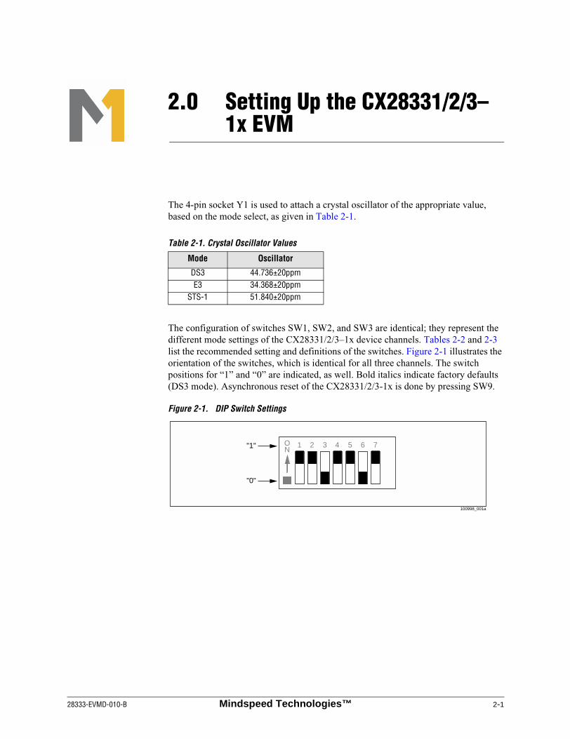
The 4-pin socket Y1 is used to attach a crystal oscillator of the appropriate value, based on the mode select, as given in Table 2-1.
The configuration of switches SW1, SW2, and SW3 are identical; they represent the different mode settings of the CX28331/2/3–1x device channels. Tables 2-2 and 2-3 list the recommended setting and definitions of the switches. Figure 2-1 illustrates the orientation of the switches, which is identical for all three channels. The switch positions for “1” and “0” are indicated, as well. Bold italics indicate factory defaults (DS3 mode). Asynchronous reset of the CX28331/2/3-1x is done by pressing SW9.
Table 2-1. Crystal Oscillator Values
Mode Oscillator
DS3 44.736±20ppmE3 34.368±20ppm
STS-1 51.840±20ppm
Figure 2-1. DIP Switch Settings
100998_001a
1 2 3 4 5 6 7ON"1"
"0"
Mindspeed Technologies™ 2-1

Setting Up the CX28331/2/3–1x EVM CX28331/2/3-1x EVM User Guide
Table 2-3 describes the switch setting for the SW4 DIP switch, which is used for global selection of operating mode and whether or not the encoder/decoder is disabled.
Table 2-2. SW1, SW2, and SW3 Settings
SwitchPosition Setting Operation
1 Controls the power-down mode pin PDB
On The power-down mode is not operational for this channel.
Off This channel is in power-down mode.
2 Controls the RLOOP pin or remote loopback option
On Remote loopback is enabled.
Off Remote loopback is disabled.
3 Controls the LLOOP pin or the local loopback option
On Local loopback is enabled.
Off Local loopback is disabled.
4 Controls the line build out pin LBO
On Transmit cable is shorter than 450 ft., set it to On.
Off Transmit cable is longer than 450 ft., set it to Off.
5 Controls the transmitter enable/disable pin XOE
On The transmitter is enabled.
Off The transmitter is disabled.
6 Controls the transmit alarm indicate signal TAIS pin *
On LIU Transmits all ones (AIS).
Off Normal LIU operation.
7 Controls the equalizer gain in the receiver
On The equalizer gain is high, required for DS3/STS-1 shaped pulses.
Off The equalizer operates in low gain mode suitable for square pulses (E3 mode).
* Remote Loopback (RLOOP) takes precedence over TAIS. An input clock must be present on TCLK for TAIS operation.
Table 2-3. SW4 Setting (1 of 2)
SwitchPosition Position Operation
1 Controls the E3 mode pin for all channels
On E3 mode is selected.
Off DS3/STS-1 mode is selected.
2-2 Mindspeed Technologies™ 28333-EVMD-010-B
CX28331/2/3-1x EVM User Guide Setting Up the CX28331/2/3–1x EVM
Jumpers J8, J9 and J10 are connected to enable the Receive Loss of Signal (RLOS) indicators - LEDs CR1, CR2 and CR3 for channels 1, 2 and 3, respectively. When the LED is on, it is a visual signal that the channel is experiencing a Receive Loss of Signal. Refer to Table 2-4.
Connector J11 provides access to the digital input/output signals that interface to an external framer device. From this connector the user has the ability to evaluate the received rail/NRZ data and clock as well as provide transmit rail/NRZ data and a clock. The RECLK pin provides access to the oscillator clock provided to the LIU REFCLK pins.
2 Controls the ENDECDIS pin for all channels
On Encoder/decoder is disabled to put rail data on the positive and negative data pins.
Off Encoder/decoder is enabled and data is only present on positive rail (NR2 data pin).
Table 2-3. SW4 Setting (2 of 2)
SwitchPosition Position Operation
Table 2-4. RLOS Indicators
LED Channel
CR1 1CR2 2CR3 3
NOTE: Since no framer exists on this board, it is expected that the device will normally be evaluated using the remote loopback feature inside the LIU.
28333-EVMD-010-B Mindspeed Technologies™ 2-3

Setting Up the CX28331/2/3–1x EVM CX28331/2/3-1x EVM User Guide
Table 2-5. Connector J11 Digital Rail/NRZ Data Signals
Pin Description Pin Description
1 GND 2 TCLK13 GND 4 TNEG1/NC15 GND 6 TPOS1/TNRZ17 GND 8 RCLK19 GND 10 RNEG1/RLCV1
11 GND 12 RPOS1/RNRZ113 GND 1415 GND 16 TCLK217 GND 18 TNEG2/NC219 GND 20 TPOS2/TNRZ221 GND 22 RCLK223 GND 24 RNEG2/RLCV225 GND 26 RPOS2/RNRZ227 GND 2829 GND 30 TCLK331 GND 32 TNEG3/NC333 GND 34 TPOS3/TNRZ335 GND 36 RCLK337 GND 38 RNEG3/RLCV339 GND 40 RPOS3/RNRZ341 GND 4243 GND 44 REFCLK
2-4 Mindspeed Technologies™ 28333-EVMD-010-B

28333-EVMD-010-B
3.0 Jumper and Switch Connections
3.1 Jumper Connections
Jumpers J8, J9 and J10 are used to isolate the LED’s from being driven by the CX28331/2/3-1x for debug purposes. Jumper J7 is used to select if a 3.3 V or 5 V supply is to be connected to the VGG pin on the CX28331/2/3–1x; the default is for VGG to be connected to 3.3 V. Jumper J16 is used for current measurement and is generally left unconnected.
3.2 Items Not in Final DesignSW5, J14 and J15 are shown in the board schematic, but are depopulated; they are for Mindspeed internal testing only. They should not be added in your final design. Jumpers J12 and J13 are populated, but are intended for internal factory test purposes.
Mindspeed Technologies™ 3-1

Jumper and Switch Connections CX28331/2/3-1x EVM User Guide
3-2 Mindspeed Technologies™ 28333-EVMD-010-B

28333-EVMD-010-B
4.0 Schematics, Silkscreen and Board Layout
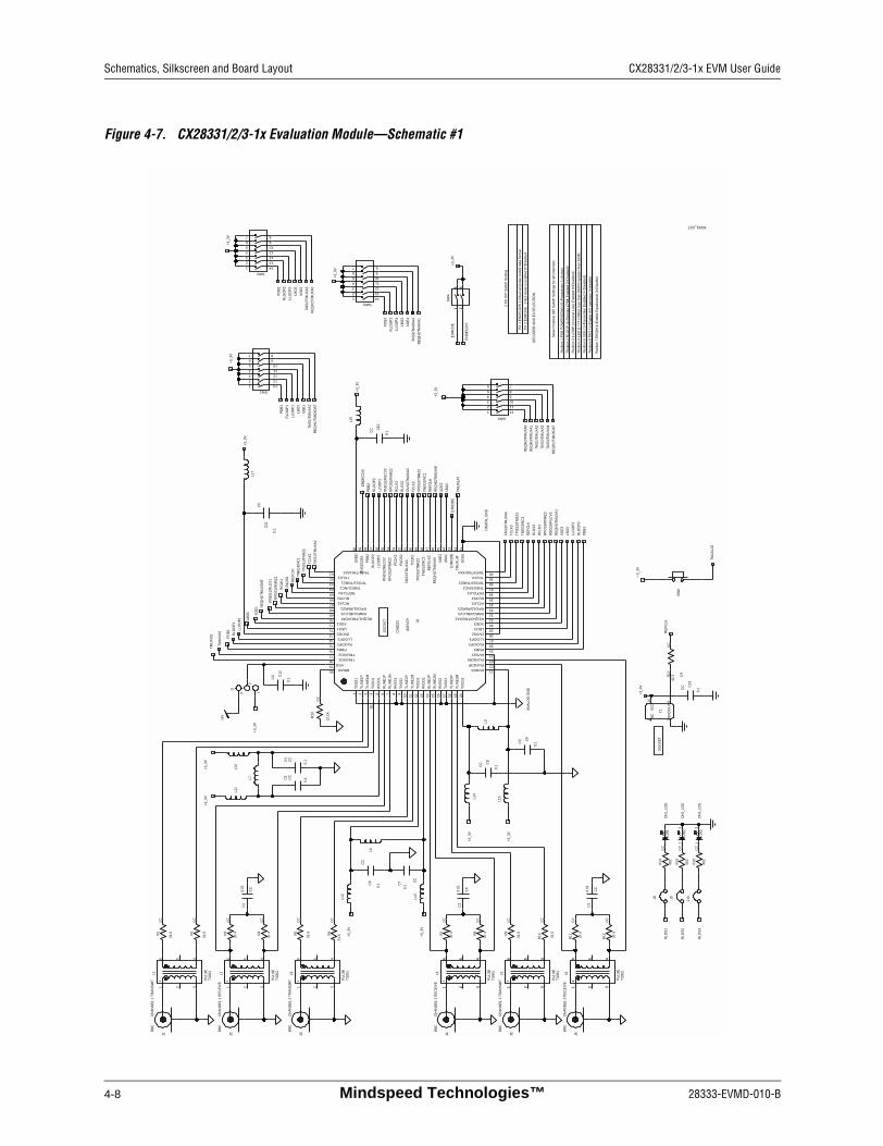
The board layout and schematic diagrams on the following pages provide the details for components and the circuits used in the EVM.
Mindspeed Technologies™ 4-1

Schematics, Silkscreen and Board Layout CX28331/2/3-1x EVM User Guide
Figure 4-1. CX28331/2/3-1x Evaluation Module
8333
_021
4-2 Mindspeed Technologies™ 28333-EVMD-010-B

CX28331/2/3-1x EVM User Guide Schematics, Silkscreen and Board Layout
Figure 4-2. CX28331/2/3-1x Evaluation Module—Layer 1
8333
_025
28333-EVMD-010-B Mindspeed Technologies™ 4-3

Schematics, Silkscreen and Board Layout CX28331/2/3-1x EVM User Guide
Figure 4-3. CX28331/2/3-1x Evaluation Module—Layer 2
8333
_023
4-4 Mindspeed Technologies™ 28333-EVMD-010-B

CX28331/2/3-1x EVM User Guide Schematics, Silkscreen and Board Layout
Figure 4-4. CX28331/2/3-1x Evaluation Module—Layer 3
8333
_024
28333-EVMD-010-B Mindspeed Technologies™ 4-5
Schematics, Silkscreen and Board Layout CX28331/2/3-1x EVM User Guide
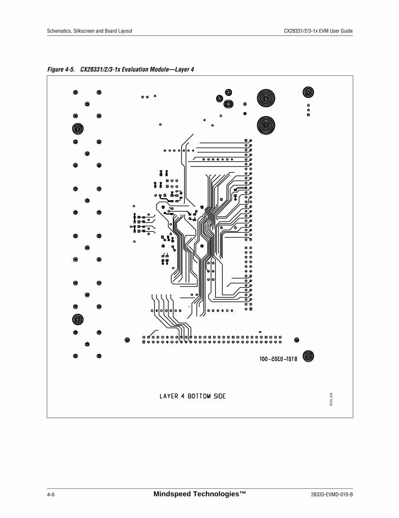
Figure 4-5. CX28331/2/3-1x Evaluation Module—Layer 4
8333
_026
4-6 Mindspeed Technologies™ 28333-EVMD-010-B
CX28331/2/3-1x EVM User Guide Schematics, Silkscreen and Board Layout
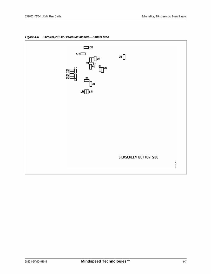
Figure 4-6. CX28331/2/3-1x Evaluation Module—Bottom Side
8333
_022
28333-EVMD-010-B Mindspeed Technologies™ 4-7
Schematics, Silkscreen and Board Layout CX28331/2/3-1x EVM User Guide
Figure 4-7. CX28331/2/3-1x Evaluation Module—Schematic #1
Posi
tion
7 R
EQ
H(1
=Ena
ble
Equ
aliz
atio
n 0=
Dis
able
)
Pin
2 E
3MO
DE
1=
E3
mod
e is
ena
bled
0=D
isab
led
Pin
1 E
ND
EC
DIS
1=D
ual r
ail p
ulse
cod
ed d
ata
form
at
SO
CK
ET
SO
CK
ET
CH
AN
NE
L 3
RE
CE
IVE
CH
AN
NE
L 3
TRA
NS
MIT
CH
AN
NE
L 2
RE
CE
IVE
DE
CO
DE
R A
ND
E3
SE
LEC
TIO
N
CH
AN
NE
L 1
RE
CE
IVE
CH
AN
NE
L 1
TRA
NS
MIT
CH
AN
NE
L 2
TRA
NS
MIT
Posi
tion
1 P
DB
PO
WE
RD
OW
N (0
=Pow
erdo
wn
1=A
ctiv
e)
Posi
tion
2 R
LOO
P (1
=Rem
ote
LPB
K E
nabl
ed 0
=Dis
able
d)
Posi
tion
3 LL
OO
P (1
=Loc
al L
oop
Ena
bled
0=D
isab
led)
Posi
tion
4 LB
O (1
=TX
CA
BLE
less
than
250
ft 0=
grea
ter t
han
250f
t)
Posi
tion
5 X
OE
(1=T
rans
mitt
er E
nabl
ed 0
=Dis
able
d)
Posi
tion
6 TA
IS (1
=Ena
ble
AIS
ope
ratio
n 0=
disa
ble)
DIG
ITA
L G
ND
BN
C
BN
C
BN
C
BN
C
BN
C
CC
CC
CC
CC
CC
CC
CC
BN
C
CC
AN
ALO
G G
ND
CC
CC
CC
CC
CC
CC
CC
2 P
in D
IP S
witc
h S
ettin
g
Sev
en P
ositi
on D
IP S
witc
h S
ettin
gs fo
r all
Cha
nnel
s
CC
CC
CC
CC
CC
CC
CC
CC
CC
CC
CC
CC
CC
CC
CC
CH
1_LO
S
CH
2_LO
S
CH
3_LO
S
7
8
9
6
5
4
3
2
12
11
10
1
SW5
N1
T300
1P
ULS
E
1 2 3456
L2
T300
1P
ULS
E
1 2 3456
L3
1 2 3456
T300
1P
ULS
E
6 5 4321
L4
1 2 3456
T300
1P
ULS
E
6 5 4321
L5
1 2 3456
T300
1P
ULS
E
1 2 3456
L6
J2 J3 J4 J5 J6
R3
37.4
37.4R4
R7
37.4
37.4R8
0.01
C2
R11 37
.4
0.01
C3
R12 37
.4
J1
T300
1P
ULS
E
6 5 4321
L1
1 2344 3
21
SW
4
J8 J9 J10
14 871
Y1
21
CR
3
C1
0.01
31.6R1
R2
31.6
31.6R5
31.6R9
31.6
R10
L15
L7
L11
L10
C4
0.1
0.1C
5
R6
31.6
L13
L12
C6
0.1
L8
0.1C
7
L14
L9C
8
0.1
12.1
K
R13
CR
1
12
CR
2
SW
9
C9
0.1
5 10
3
4
6
8
9
11
1
2
7
13
12
14
SW1
5 10
3
4
6
8
9
11
1
2
7
13
12
14
SW25 10
3
4
6
8
9
11
1
2
7
13
12
14
SW3
R14
402
402
R15
402
R16
1/4
42.2R
17
C10
0.1
L16
L17
C11
0.1
60
73
41
28
4359
31
72
44
29
74
56
27
76
58
25
80
67
53
34
65
47
36
70
46
76
1514
23
22
75
57
26
66
52
35
69
55
32
68
54
33
5
13
21
8
16
24
61
51
40
62
32
1110 1918
78
77
42
64
63
49
38
4
12 20
1 9
17
79
71
45
30
80E
XFP
CN
8333
50 48
39
37
U1
0.1
C12
C13
0.1
2
3 1
J7
TAIS
3/TM
UX
A4
XO
E3
LBO
3
LLO
OP
3
PD
B3
RLO
OP
3
+3_3
V
TAIS
1/TM
UX
A2
XO
E1
LBO
1
LLO
OP
1
PD
B1
RLO
OP
1
+3_3
V
RLO
S1
RLO
S2
RLO
S3
GN
D
NC
OU
T
VC
C
+3_3
V
+3_3
V
+3_3
V
+3_3
V+3
_3V
+3_3
V
+3_3
V
+5V
TMU
XIO
1
TMU
XIO
2
PD
B1
RLO
OP
1
LLO
OP
1 LBO
1 XO
E1 R
EQ
H1/
TMU
XD
AT
RN
EG
1/R
LCV
1
RP
OS
1/R
NR
Z1
RC
LK1
RLO
S1
RE
FCLK
TNE
G1/
NC
1
TPO
S1/
TNR
Z1
TCLK
1
TAIS
1/TM
UX
A2
PD
B2
RLO
OP
2
LLO
OP
2
RN
EG
2/R
LCV
2
RP
OS
2/R
NR
Z2
RC
LK2
RLO
S2
TAIS
2/TM
UX
A3
TPO
S2/
TNR
Z2
RE
FCLK
RE
QH
2/TM
UX
A0
XO
E2
LBO
2
TMU
XLA
T
PD
B3
RLO
OP
3
LLO
OP
3
LBO
3
XO
E3
RE
QH
3/TM
UX
A1
RN
EG
3/R
LCV
3
RP
OS
3/R
NR
Z3
RC
LK3
RLO
S3
RE
FCLK
TPO
S3/
TNR
Z3
TAIS
3/TM
UX
A4
+3_3
V
+3_3
V
+3_3
V+3
_3V
+3_3
V
RLO
OP
2
PD
B2
LLO
OP
2
LBO
2
XO
E2
TAIS
2/TM
UX
A3
E3M
OD
E
EN
DE
CD
IS
EN
DE
CD
IS
E3M
OD
E
RE
QH
1/TM
UX
DAT
RE
QH
2/TM
UX
A0
RE
QH
3/TM
UX
A1
TMU
XLA
T
RE
FCLK
+3_3
V
DV
DD
DVDD2
DV
SS
DVSS2
E3M
OD
E
EN
DE
CD
IS
REQH3/TMUXA1
LBO1
LBO
2
LBO3
LLOOP1
LLO
OP
2
LLOOP3
PDB1
PD
B2
PDB3
RBIAS
RCLK1
RC
LK2
RCLK3
REFCLK1
RE
FCLK
2
REFCLK3
REQH1/TMUXDAT
RE
QH
2/TM
UX
A0
RLI
NE
1M
RLI
NE
1P
RLI
NE
2M
RLI
NE
2P
RLINE3M
RLINE3P
RLOOP1
RLO
OP
2
RLOOP3
RLOS1
RLO
S2
RLOS3
RNEG1/RLCV1
RN
EG
2/R
LCV
2
RNEG3/RLCV3
RPOS1/RNRZ1
RP
OS
2/R
NR
Z2
RPOS3/RNRZ3
RV
DD
1
RV
DD
2
RVDD3
RV
SS
1
RV
SS
2
RVSS3
TAIS1/TMUXA2
TAIS
2/TM
UX
A3
TAIS3/TMUXA4
TCLK1
TLIN
E1M
TLIN
E1P
TLIN
E2M
TLIN
E2P
TLIN
E3M
TLIN
E3P
TMUXIO1
TMUXIO2
TMU
XLA
T
TNEG1/NC1
TPOS1/TNRZ1 TPO
S2/
TNR
Z2
TPOS3/TNRZ3
TVD
D1
TVD
D2
TVD
D3
TVS
S1
TVS
S2
TVS
S3
VGG
XOE1
XO
E2
XOE3
TCLK
2
TNE
G2/
NC
2
TCLK3
TNEG3/NC3
TCLK
2
TNE
G2/
NC
2
TCLK
3
TNE
G3/
NC
3
+3_3
V
RE
QH
2/TM
UX
A0
RE
QH
3/TM
UX
A1
TAIS
1/TM
UX
A2
TAIS
2/TM
UX
A3
TAIS
3/TM
UX
A4
RE
QH
1/TM
UX
DAT
8333_027
4-8 Mindspeed Technologies™ 28333-EVMD-010-B

CX28331/2/3-1x EVM User Guide Schematics, Silkscreen and Board Layout
Figure 4-8. CX28331/2/3-1x Evaluation Module—Schematic #2
GREEN
used for heat sink.1 square inch copper plane
NO LOAD
Ground
+5 Volts
Power Supply
Mount these parts close together.
CHASSIS GND
CHASSIS GND
NO LOAD
POWER
SWAGE
CC
CC
CC+
CC+
BJACK
BJACK
CC
CC
1 32
+3_3VREG
321
VR1
E1
1
2CR12
CR13
1 2
POLYSWITCH
21
SMD200-2
FS1
ZERO
R29
330
R30
C17
1025V
C18
22010V
12
J16
1
3
2
J17
RED_BANNANAJ18
BLACK_BANNANAJ19
J20
C16
0.1
C19
0.1
+5V
GN
D
VIN
VO
UT
+3_3V
SHUNT
PIN
SLEEVE
8333_029
28333-EVMD-010-B Mindspeed Technologies™ 4-9

Schematics, Silkscreen and Board Layout CX28331/2/3-1x EVM User Guide
4-10 Mindspeed Technologies™ 28333-EVMD-010-B

28333-EVMD-010-B
5.0 Parts Specifications and Dimensions
5.1 Suggested Vendor Information
General Electronic Devices (Xtal)320 So. Pacific St.San Marcos, CA 92069 Tel: (760) 591-4170Fax (760) 591-4164Email:[email protected]: www.gedlm.com
Crystek Corporation (Xtal)12730 Commonwealth Drive Fort Myers, Fl 33913Tel: (800) 237-3061Fax: (941) 561-1025Email: [email protected]: www.crystek.com
Pulse Engineering (Xfmers)12220 World Trade DriveSan Diego, CA 92128Tel: (858) 674-8307Fax: (858) 385-8000Email: [email protected]: www.pulseeng.com
Digi-KeyWebsite: www.digi-key.com
Allied ElectronicsWebsite: www.allied.avnet.com
Mindspeed Technologies™ 5-1

Parts Specifications and Dimensions CX28331/2/3-1x EVM User Guide
5-2 Mindspeed Technologies™ 28333-EVMD-010-B

28333-EVMD-010-B
6.0 Technical Support and Documentation
For technical questions, contact a field applications engineer (FAE) located at the Mindspeed Technologies sales office in your region. See the Mindspeed Technologies Web site (www.mindspeed.com) for a list of worldwide sales offices.
For additional documentation and/or current revisions, go to our Web site (www.mindspeed.com), enter CX28333 in the Product/Document Search window, and select the Go button.
Mindspeed Technologies™ 6-1

Technical Support and Documentation CX28331/2/3-1x EVM User Guide
6-2 Mindspeed Technologies™ 28333-EVMD-010-B

www.mindspeed.com
General Information:U.S. and Canada: (800) 854-8099International: (949) 483-6996Headquarters—Newport Beach4000 MacArthur Blvd., East TowerNewport Beach, CA 92660


