Page 1
FUNDAMENTAL STUDIES OF COPPER CORROSION IN
INTERCONNECT FABRICATION PROCESS AND SPECTROSCOPIC
INVESTIGATION OF LOW-k STRUCTURES
Arindom Goswami, M.S., M.Sc.
Requirements for the Degree of
DOCTOR OF PHILOSOPHY
UNIVERSITY OF NORTH TEXAS
December 2015
APPROVED:
Oliver M. R. Chyan, Major Professor
Michael G. Richmond, Committee Member
Teresa Golden, Committee Member
William E. Acree, Committee Member &
Chair of the Department of Chemistry
Costas Tsatsoulis, Dean of the Toulouse
Graduate School
Page 2
Goswami, Arindom. Fundamental Studies of Copper Corrosion in Interconnect
Fabrication Process and Spectroscopic Investigation of Low-k Structures. Doctor of Philosophy
(Chemistry -Analytical Chemistry), December 2015, 87 pages, 2 tables, 40 figures, chapter
references.
In the first part of this dissertation, copper bimetallic corrosion and its inhibition in
cleaning processes involved in interconnect fabrication is explored. In microelectronics
fabrication, post chemical mechanical polishing (CMP) cleaning is required to remove organic
contaminants and particles left on copper interconnects after the CMP process. Use of cleaning
solutions, however, causes serious reliability issues due to corrosion and recession of the
interconnects. In this study, different azole compounds are explored and pyrazole is found out to
be a potentially superior Cu corrosion inhibitor, compared to the most widely used benzotriazole
(BTA), for tetramethyl ammonium hydroxide (TMAH)-based post CMP cleaning solutions at pH
14. Micropattern corrosion screening results and electrochemical impedance spectroscopy (EIS)
revealed that 1 mM Pyrazole in 8 wt% TMAH solution inhibits Cu corrosion more effectively
than 10 mM benzotriazole (BTA) under same conditions. Moreover, water contact angle
measurement results also showed that Pyrazole-treated Cu surfaces are relatively hydrophilic
compared to those treated with BTA/TMAH. X-ray photoelectron spectroscopy (XPS) analysis
supports Cu-Pyrazole complex formation on the Cu surface. Overall Cu corrosion rate in
TMAH-based highly alkaline post CMP cleaning solution is shown to be considerably reduced to
less than 1Å/min by addition of 1 mM Pyrazole.
In the second part, a novel technique built in-house called multiple internal Reflection
Infrared Spectroscopy (MIR-IR) was explored as a characterization tool for characterization of
different low-k structures.In leading edge integrated circuit manufacturing, reduction of RC time
Page 3
delay by incorporation of porous ultra low-k interlayer dielectrics into Cu interconnect
nanostructure continues to pose major integration challenges. The main challenge is that porous
structure renders interlayer dielectrics mechanically weak, chemically unstable and more
susceptible to the RIE plasma etching damages. Besides the challenge of handling weak porous
ultra low-k materials, a lack of sensitive metrology to guide systematic development of plasma
etching, restoration and cleaning processes is the major stumbling block. We explored Multiple
Internal Reflection Infrared Spectroscopy and associated IR techniques as a sensitive (sub-5 nm)
characterization tool to investigate chemical bonding modification across fluorocarbon etch
residues and low-k dielectric interface after plasma etching, ashing, UV curing and post-etch
cleaning. The new insights on chemical bonding transformation mapping can effectively guide
the development of clean-friendly plasma etch for creating ultra low-k dielectric nanostructures
with minimal dielectric damages.
Page 4
ii
Copyright 2015
By
Arindom Goswami
Page 5
iii
ACKNOWLEDGEMENTS
Six years ago, I arrived in the USA from India to pursue higher studies. After six years,
this journey is on the verge of completion with the grace of God. I take this opportunity to
express my sincere gratitude to all those who have encouraged and believed in me to complete
this dissertation.
First and foremost, I would like to thank my mother Rajalakhmi and sister Lakhirupa for
supporting me in this journey.
I shall forever remain grateful to my PhD advisor Dr. Chyan for taking me under his
wings and making me a good student as well as a better person. I would like to thank my
committee members Dr. Acree, Dr. Richmond and Dr. Golden for their comments and critiques
of my dissertation in a short span of time which greatly helped me improve my dissertation and
make it better. I would also like to thank all my friends and team members for their constant
support: Nick Ross, Sirish Rimal, Tamal Mukherjee, Pofu Lin, Dr. Seare Berhe, and past
graduates Dr. Simon Koskey, Dr. Jafar Abdelghani. Sirish Rimal and Tamal Mukherjee deserve
special mention as they contributed heavily in writing chapter 3, both with their scientific input
as well as with MIR-IR and UV irradiation experiments. I would also like to thank CART,
especially Saul for being helpful.
The financial support from the chemistry department, SRC, INTEL, TEL, ATMI, LAM
research, and Freescale semiconductor is deeply appreciated.
Lastly and most importantly, I would like to say a big thank you to my late father Dr.
Aboni Chandra Goswami for having been such a wonderful father and for touching each of our
lives and making it beautiful. I miss you every day. I wish you were here to see this moment.
This dissertation is dedicated to you.
Page 6
iv
CONTENTS
ACKNOWLEDGEMENTS iii
LIST OF FIGURES AND TABLES viii
CHAPTERS
Chapter 1 Introduction and instrumentation 1
1.1 Introduction 1
1.2 Copper Technology 3
1.2.1 Copper as a replacement for Aluminum 3
1.2.1.1 Low Resistivity 4
1.2.1.2 High Electromigration Resistance 5
1.2.2 Challenges to implement Copper 7
1.3 Need for planarization: CMP process for Copper 9
1.4 Chemical Mechanical Planarization (CMP) 10
1.4.1 Introduction 10
1.4.2 Copper CMP 12
1.5 Pourbaix Diagram 14
1.6 Experimental Procedure and Instruments 18
1.6.1 Potentiodynamic polarization plots 18
1.6.2 Impedance Measurements 20
1.6.3 X-Ray Photoelectron Spectroscopy (XPS) 22
Page 7
v
1.6.3.1 Introduction and Fundamentals 22
1.6.3.2 Instrumentation 26
1.6.4 Contact angle measurements 28
1.6.5 Physical vapor deposition 29
1.6.6 Micropattern corrosion screening 31
1.6.7 MIR-IR metrology 32
1.7 References 34
Chapter 2 Study of Pyrazole as Copper corrosion inhibitor in model alkaline post chemical
mechanical polishing cleaning solution 39
2.1 Introduction 39
2.2 Literature survey of inhibitor performance 43
2.2.1 The structure of copper-azole complexes 43
2.2.2 Benzotriazole 44
2.2.3 Pyrazole 46
2.3 Experimental procedure 47
2.4 Results and Discussion 49
2.4.1 Effect of substrate on Cu corrosion 49
2.4.2 Cu micropattern corrosion and inhibition 51
2.4.3 Electrochemical Analysis 54
2.4.3.1 Tafel plots 54
2.4.3.2 Electrochemical Impedance Spectroscopy (EIS) 55
2.4.4 Water Contact Angle Measurements 56
Page 8
vi
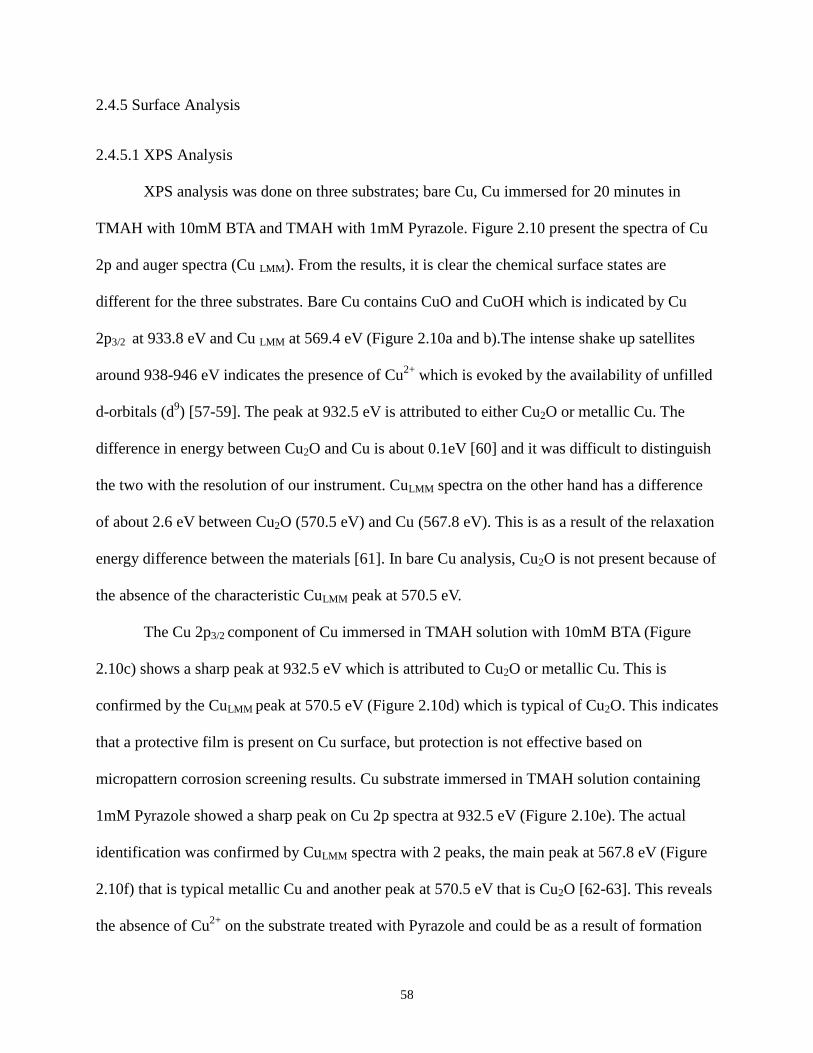
2.4.5 Surface Analysis 58
2.4.5.1 XPS Analysis 58
2.5 Proposed Mechanism of Cu Corrosion 60
2.6 Summary 61
2.7 References 61
Chapter 3 Infrared Spectroscopic Characterization on Low-k Dielectric Nanostructure to
Optimize Cu Interconnect Fabrication 66
3.1 Introduction 66
3.2 Experimental Procedure 68
3.2.1 Characterization of Dielectric Trench Pattern 68
3.2.2 Functional Group Specific Chemical Reaction 68
3.2.3 UV Treatment + Wet Clean 69
3.3 Results and Discussions 69
3.3.1 Chemical Bonding Mapping of Low-k Trench Structure after Fluorocarbon
Plasma Etch 69
3.3.2 MIR-IR Evaluation of Plasma Damage to Trench Low-k from Different
Oxidative Strip Processes 72
3.3.3 Characterization of Chemical Bonding Structure of Model Fluorocarbon
Polymer 74
3.3.4 Wet Clean of Post-Plasma Etch Residues 78
3.3.5 UV-Assisted Wet Clean of Fluorocarbon Polymer 79
3.3.6 Mechanism of UV-Induced Structural Disintegration of Fluorocarbon
Page 9
vii
Polymer 84
3.4 Conclusion 85
3.5 References 86
Page 10
viii
LIST OF FIGURES AND TABLES
Chapter 1
Figure 1.1 The effect of feature size on the gate and interconnect delay 3
Figure 1.2 Number of metal layers and k-values of ILD layers versus year of
production 7
Figure 1.3 A cross-sectional SEM image of a representative multilevel interconnect network
7
Figure 1.4 (a) Dual damascene process. 9
Figure 1.5 A cross-sectional SEM image of a representative multilevel interconnect network with
(right) and without (left) CMP process 9
Figure 1.6 Schematic of a CMP tool 11
Figure 1.7 Potential-pH equilibrium diagram for copper-water system at 25°C 13
Figure 1.8 Basic regions in a Pourbaix diagram 15
Figure 1.9 A typical Potentiodynamic polarization plot of Cu electrode shows Ecorr, Icorr, cathodic
curve, and anodic curve. 20
Figure 1.10 Nyquist plot and equivalent circuit 21
Figure 1.11 Schematic representation of the XPS instrumentation. 23
Figure 1.12 Schematic diagram of the XPS process, showing photo-electron effect. 23
Figure 1.13 (a) XPS chamber in (b) PHI 5000VersaProbe™ Scanning XPS 28
Figure 1.14 A sessile liquid drop on a solid surface in equilibrium with the vapor
Phase 29
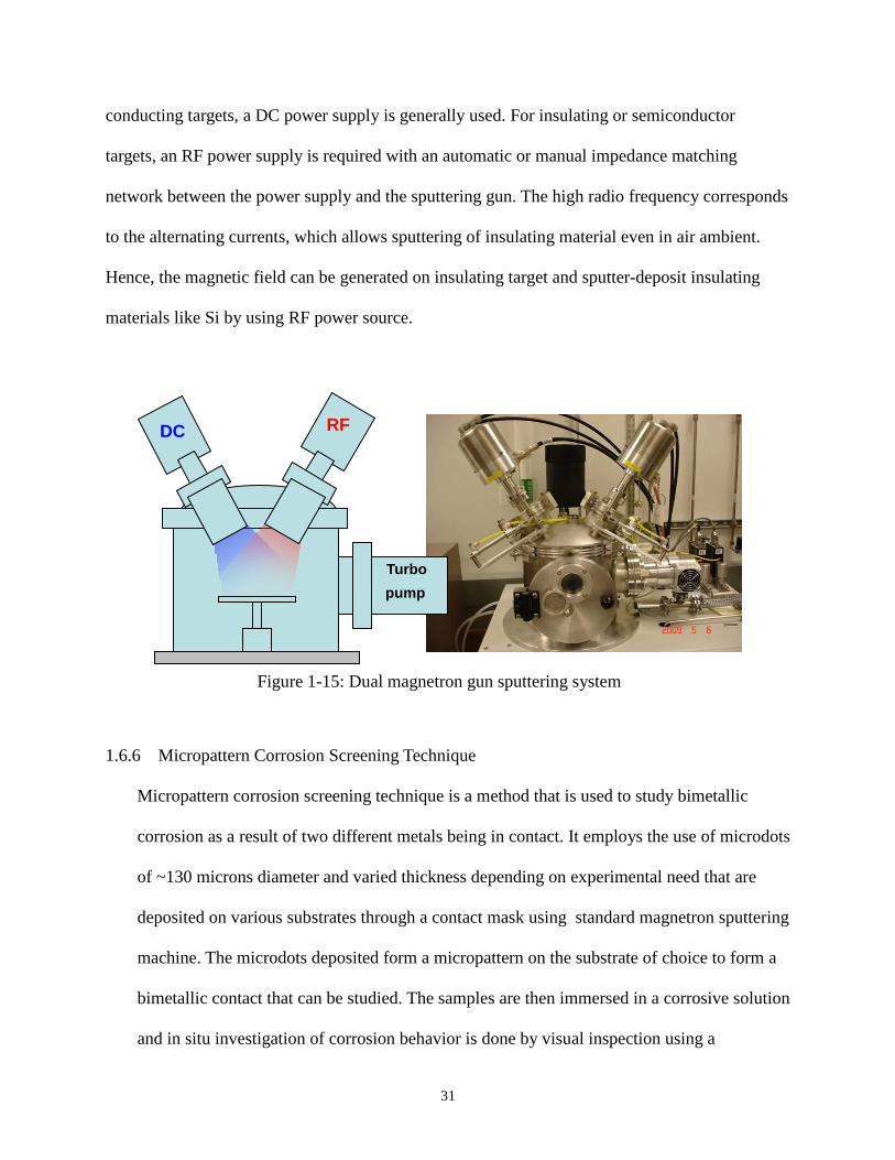
Figure 1.15 Dual magnetron gun sputtering system 31
Figure 1.16: Micropattern Corrosion Screening Technique 32
Page 11
ix
Figure 1.17: Principle of MIR-IR metrology. 33
Figure 1.18: Schematic representation of MIR-IR setup. 34
Chapter 2
Figure 2.1 Structure of benzotriazole (BTA) and Pyrazole 43
Figure 2.2 Micropattern corrosion screening structure 48
Figure 2.3 Time lapsed images of Cu microdots deposited on Ru, Ta and glass in 8 wt.% TMAH
solution 50
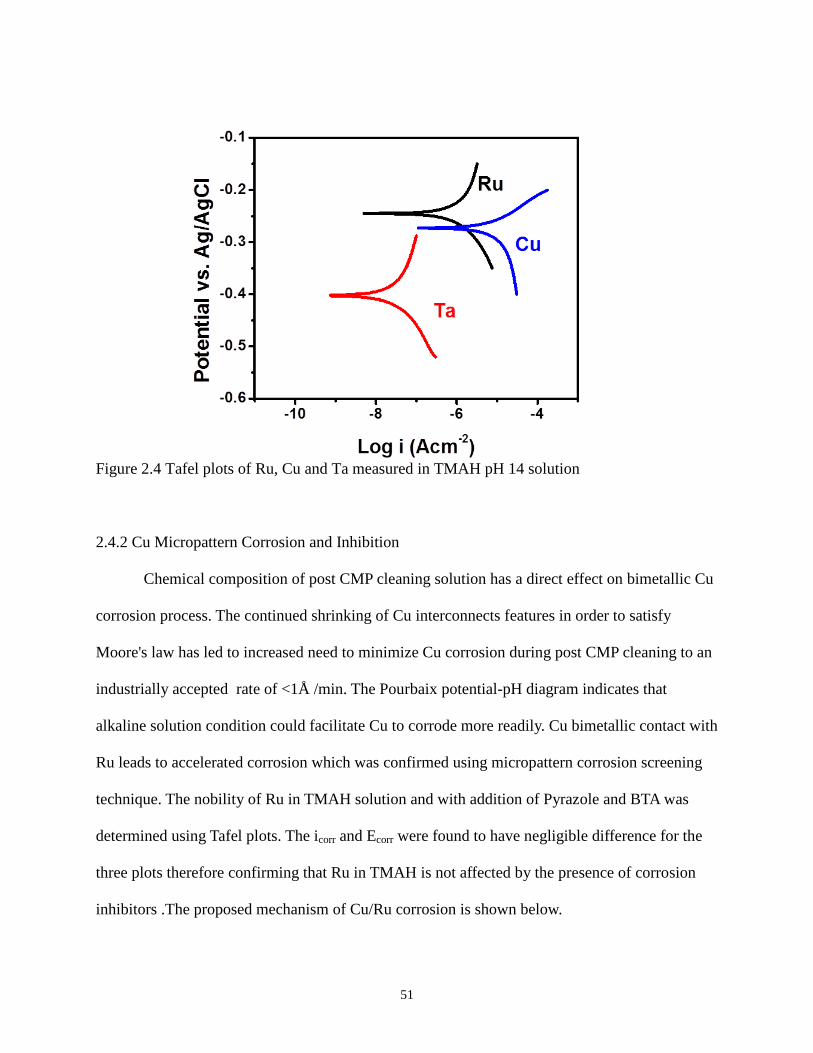
Figure 2.4 Tafel plots of Ru, Cu and Ta measured in TMAH pH 14 solution 51
Figure 2.5 Inhibitor concentration dependent etch rate of Cu in 8 wt.% TMAH 53
Figure 2.6 Time lapsed images of 50nM Cu/Ru immersed in 8 wt.% TMAH with additional
1mM Pyrazole and 10mM BTA 53
Figure 2.7 Tafel plots of Cu in 8wt.% TMAH and with Pyrazole and BTA 54
Figure 2.8 EIS data (a) Nyquist plot of Cu in TMAH (black), TMAH +BTA (red) and
TMAH+Pyrazole (blue) and inset equivalent circuit used to fit data. 56
Figure 2.9 Variation in DI water contact angle of Cu in TMAH and TMAH+ inhibitor 57
Figure 2.10 XPS Cu 2p spectra of; (a) bare Cu, (b) BTA modified Cu and (c) Pyrazole modified
Cu and Cu LMM spectra of; (d) bare Cu, (e) BTA modified Cu and (f) Pyrazole modified Cu 59
Figure 2.11 Figure 2.11 XPS N1s spectra of: (a) bare Cu, (b) BTA modified Cu and (c) Pyrazole
modified Cu 60
Chapter 3
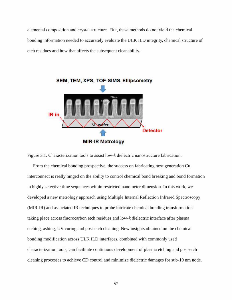
Figure 3.1 Characterization tools to assist low-k dielectric nanostructure fabrication. 67
Page 12
x
Figure 3.2 IR spectra of 300 nm CDO film obtained from MIR-IR and T-IR; mabs =
miliabsorbance unit. 70
Figure 3.3 Chemical bonding mapping of low-k trench nano-structure formed after fluorocarbon
plasma etch process. 71
Figure 3.4 (a) MIR-IR spectra of low-k trench structures after different oxidative plasma strip
processes (strip 1 – 4) to optimize O radical content and (b) respective plot of OH
increase and Si-CH3 decrease from MIR-IR and T-IR respectively. 73
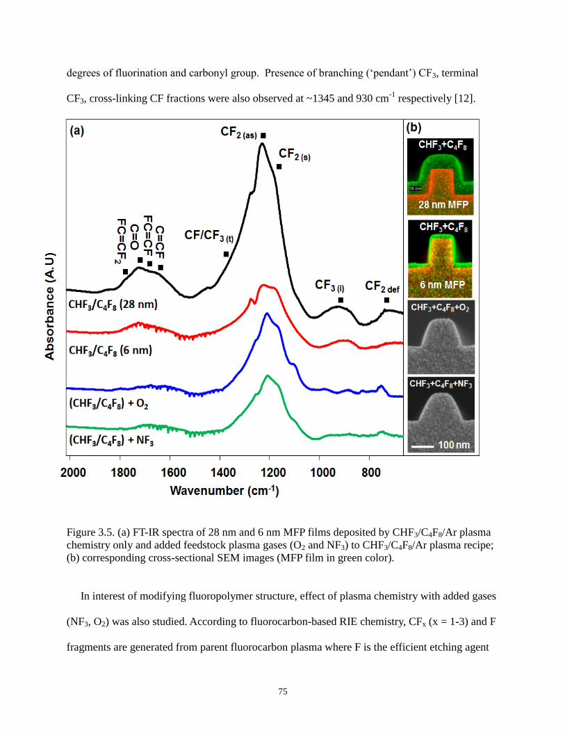
Figure 3.5 (a) FT-IR spectra of 28 nm and 6 nm MFP films deposited by CHF3/C4F8/Ar plasma
chemistry only and added feedstock plasma gases (O2 and NF3) to CHF3/C4F8/Ar
plasma recipe; (b) corresponding cross-sectional SEM images (MFP film in green
color). 75
Figure 3.6 Representative model chemical bonding structure of functionalized fluorocarbon
polymer derived via reductive defluorination of CFx groups, DNPH hydrazine
formation of carbonyl and bromination of olefin unsaturations. Differential spectra
(i) were obtained by subtracting as-deposited MFP film spectra (ii) from the
corresponding derivatized MFP film spectra (iii). 76
Figure 3.7 Time dependent proprietary cleaning solvent treatment for post-etch residue removal
on patterned low-k test wafer. 79
Figure 3.8 FT-IR spectra of as-deposited (no UV) 28 nm MFP film, 180 sec UV-treated and 300
sec UV-treated MFP film with subsequent wet clean. 81
Figure 3.9 XPS analysis of (a) C 1s and (b) F 1s of UV- treated and subsequent wet cleans on
MFP, (c) SEM images of the corresponding UV and wet cleans on MFP film. 82
Figure 3.10 IR spectroscopic evidence of progressive hydroxyl formation during UV-air
Page 13
xi
treatment that turn the fluoropolymer film more hydrophilic for improved wet
removal. 83
Figure 3.11 Proposed mechanism of UV-assisted fluorocarbon chain dissociation involving
excited singlet oxygen via photosensitization of carbonyl
groups. 84
Tables
Table 1.1 Properties of Low Resistivity Metals 5
Table 1.2 Effects of potential variation in the positive (noble) and negative (active)
directions 16
Page 14
1
CHAPTER 1
INTODUCTION AND INSTRUMENTATION
1.1 Introduction
Advanced and sophisticated electronic gadgets such as high speed computers with quad-
core processors and terabit hard disk drives, smartphones, video games with vivid graphics – just
to name a few, have penetrated into every aspects of our daily life. These wonders of technology
with enhanced performance were invented due to the speedy growth of the semiconductor chip
manufacturing and technology. Microprocessor chips are the most complex manufactured
product known till date. For example, approximately 400 of 45nm transistors could fit on the
surface of a single human red blood cell [1]. The number of devices on a chip for silicon
integrated circuits follows an extraordinary growth as predicted by Gordon Moore [2], allowing
billions of transistors to be integrated on a single chip. This increase in device density has
resulted in constant improvement in cost and performance.
Prior devices with feature sizes of 1 m and higher have utilized aluminum-based
materials (resistivity- 2.6 -cm) for the interconnect fabrication effectively. However, it is
possible to amplify the device speed by utilizing lower resistance metals as interconnects, such
as copper (resistivity- 1.67 -cm). The use of copper permits the reduction of resistance-
capacitance (RC) delay.
For over three decades, silicon dioxide (SiO2) has been the dielectric material of choice
for the semiconductor chip manufacturing. But in recent times, due to the ever-increasing
demand for high processing speed in semiconductor and scaled-down chip components, SiO2 is
no longer acceptable. Thus, low-k materials have come into prominence and started to replace
Page 15
2
SiO2 as dielectric materials. By lowering the dielectric constant RC delay (R = the resistance of
the metal lines; C = the line capacitance), and metal cross-talk between wires can be reduced. In
recent years, a variety of low-k materials with a dielectric constant (k) of less than 3 have been
investigated. Ultra-low-k materials are polymeric compounds that can either be spin-coated from
a solution or plasma deposited by a chemical vapor deposition (CVD) process. In the year 2000,
IBM declared the fabrication of Cu interconnect structures for the 130-nm node with SiLK™, a
polyphenylene based material with a dielectric constant (k) of about 2.7. Carbon-doped oxide
(CDO), also called organosilicate glass (OSG), is a group of materials deposited by CVD
technique by incorporating hydrocarbon groups into oxide films (SiOCH films) and introducing
porogens into the film to create pores. Currently, CDO materials are commercially accessible
under the trade names Black Diamond™ and Coral™. They are the materials of choice for
contemporary copper dual damascene based interconnect structures [3].
In a characteristic damascene process, a hardmask is used for deposition and patterning of
the low-k material. A barrier layer (Ta) deposition is carried forward using physical vapor
deposition (PVD) technique to facilitate adhesion and to operate as a diffusion barrier between
metal and dielectric material, before inlaying the interconnect metal (Cu). Next, copper is
electroplated to a thickness of 0.5–1.0 μm above the dielectric over the whole wafer surface. The
surplus copper deposit left during this process is subsequently polished away using chemical-
mechanical polishing (CMP process) down to the barrier layer, which is then polished away,
exposing the dielectric layer.
Page 16
3
1.2 Copper technology
1.2.1 Copper as a replacement for Aluminum
In the year 1997, copper has replaced aluminum as the electrical interconnection material on
silicon integrated circuits. Low resistivity and high resistance to electromigration make copper
an attractive alternative to aluminum. As device dimensions shrink below 0.25 pm, the continued
use of aluminum interconnects became questionable. Silicon chip manufacturers have started
using copper metallization for sub-0.25 μm generation devices.
Figure 1.1: The effect of feature size on the gate and interconnect delay [4]
Desired properties of metals for ULSI: [5]
Low resistivity (< 4 µΩ-cm)
Easy to be etch
Should be stable in oxidizing environment (oxidizable)
Excellent adhesion to underlying substrate
Page 17
4
Mechanical and electrical stability
Surface smoothness
Less contamination of processing equipment
Anisotropically etchable with high selectivity with respect to substrate and mask material
Depositable over vertical walls with conformal coverage of steps
Low film stresses.
1.2.1.1 Low resistivity
The total circuit signal delay is a combination of the intrinsic device delay and the interconnect
delay. Figure 2.1 shows a comparison of the intrinsic gate delay of a metaloxide-semiconductor
transistor and the interconnect delay. As feature sizes on a silicon chip decrease (< 1 pm), the
circuit signal delay is dominated by the interconnect delay rather than the intrinsic device delay.
The delay in signal propagation through an interconnect is given by the product of resistance (R)
and capacitance (C). The RC time constant is given by equation (2.1)
(1.1)
where = interconnect resistivity, tm = interconnect thickness, L = interconnect length, =
interlayer dielectric (ILD) permittivity, and = interlayer dielectric thickness. Consequently,
the interconnect delay can be reduced by using metals with lower resistivity and/or ILDs with
lower dielectric constant. The resistivity of pure aluminum is 2.7 µΩ cm whereas that of pure
copper is considerably lower at 1.7 µΩ cm [9] Note that in practice, aluminum is alloyed with
copper and silicon to increase its electromigration resistance and decrease its reactivity. These
alloying additions increase the resistivity of the aluminum interconnect to -3.5 µΩ cm, making
copper even more attractive.
Page 18
5
Table 1.1. Properties of Low Resistivity Metals [6]
Ag Al Al alloy Au Cu
Resistivity (µΩ-
cm)
1.59 2.66 ~3.5 2.35 1.67
Electromigration
Resistance
Poor Poor Fair-Poor Very Good Good
Corrosion
Resistance
Poor Good Good Excellent Poor
Adhesion to
SiO2
Poor Good Good Poor Poor
Si Deep Levels Yes No No Yes Yes
RIE Etch No Yes Yes No No
As we can see from the table, out of all the metals with low resistivity than aluminum, copper
appears to be most attractive. Copper has a resistivity slightly greater than Ag and approximately
50 % lower than the aluminum. Thus, RC delay gets significantly reduced due to incorporation
of copper.
1.2.1.2 High electromigration resistance
The interconnect materials in integrated circuits are subjected to elevated temperatures (~100°C
due to Joule heating) and high current densities (105 - 10
6 A/cm
2) during operation. [7] Such
conditions facilitate electromigration to occur within the conductor lines, leading to considerable
mass transport in metals. As a result of electromigration, interconnect failure can occur due to
formation of pores or discontinuities in the metal.
Page 19
6
Atomic diffusion can be elevated at high operating temperatures of the interconnect. The atomic
mobility in the conductor is further enhanced due to the influence of applied electric field on the
ionized atoms. Due to the high current densities experienced by the interconnect during
operation, the momentum transfer induced by electron dictates and directs to overall mass
transfer in the route of electron flow.
The effective charge (Z*) on an atom is the sum total of the true charge on an ionized atom and a
total number of collisions per unit time between an atom and electrons. [8]
(1.2)
In equation (1.2), Z = true charge, ne = density of electrons, le = mean free path of electrons, and
= collision cross-section of atoms with electrons. Z* for aluminum is in the range (6.5-16.4)
while for copper the range is (3.7-4.3). [9] Atomic densities as well as resistivities of aluminum
and copper differ by a factor of less than 2. Hence, diffusivity is the major factor that determines
the electromigration resistance of these two metals. Copper has a significantly higher melting
point than aluminum (1084°C vs. 660°C). Therefore, the bulk diffusivity of copper at 100°C
(interconnect operating temperature) is ten orders of magnitude smaller than that of aluminum.
Hence, copper can handle higher current densities (up to 5 X 10⁶ A/cm
2) compared to aluminum
( 2 X 10⁵ A/cm
2 ).
Page 20
7
Figure 1.2: Number of metal layers and k-values of ILD layers versus year of production [10]
Figure 1.3: A cross-sectional SEM image of a representative multilevel interconnect network [11]
1.2.2 Challenges to implement copper
During processing (< 450°C) [9] and device operation (~100°C), copper is subjected to higher
temperatures. The diffusion of copper increases at higher temperatures due to the exponential
Page 21
8
dependence of the diffusion coefficient, D, on temperature given by
(1.3)
where D0 = pre-exponential diffusivity , Q = activation energy, R= gas constant, and T = absolute
temperature (K). As a result, copper can diffuse into the isolating dielectric, e.g. silicon dioxide
(SiO2). Copper diffusion into SiO2 is speeded up more by the presence of an electric field for the
duration of device operation. The occurrence of copper in SiO2 results in current leakage across
the interlayer dielectric [9].
Therefore, the use of copper as an interconnect require the use of a barrier layer to avert diffusion
into the underlying dielectric and substrate at higher processing and operating temperatures and
under applied electric field. Besides a diffusion barrier, an adhesion layer is also required as
copper does not bond well to SiO2. Another drawback of copper technology is the reactivity of
copper. Copper continues to oxidize for as long as it is exposed to the ambient environment,
unlike aluminum which forms a self-limiting oxide. The leading hurdle in incorporating copper
into prevalent silicon integrated circuit technology is patterning the interconnects. As copper
does not form volatile species below 100°C, common dry etching techniques used on aluminum
(such as, reactive ion etching) cannot be employed to pattern copper. Instead, an inlaid metal
process like the damascene approach can be used. In the damascene approach, trenches are
etched into the dielectric; a diffusion barrier/adhesion layer is deposited, followed by copper
deposition to fill the precut trenches. Excess copper is polished away by chemical mechanical
planarization (Figure 1.4). This process creates a planar surface with copper surrounded by the
diffusion barrier/adhesion layer on all sides but the polished surface. This inlaid metal structure
created with the help of CMP has been proven to be a practical manufacturing process for copper
interconnections. Damascene architecture together with CMP has been effective in creating
Page 22
9
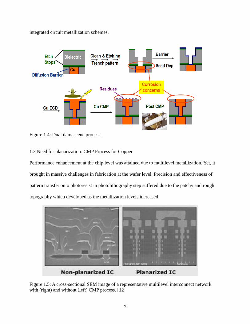
integrated circuit metallization schemes.
Figure 1.4: Dual damascene process.
1.3 Need for planarization: CMP Process for Copper
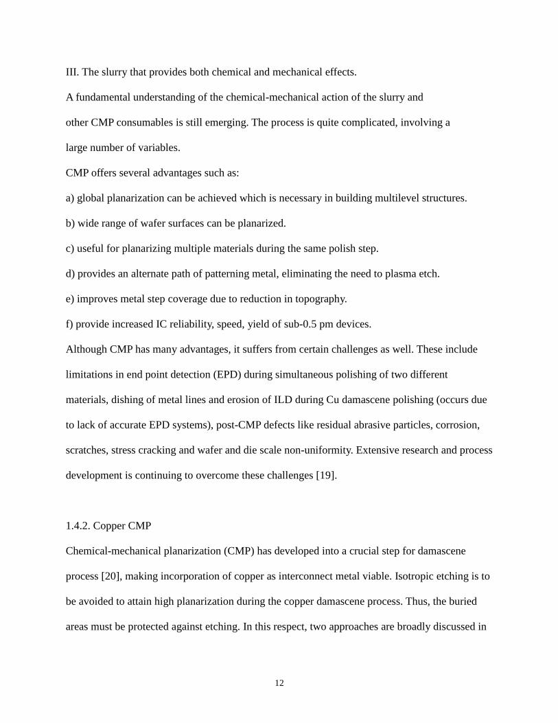
Performance enhancement at the chip level was attained due to multilevel metallization. Yet, it
brought in massive challenges in fabrication at the wafer level. Precision and effectiveness of
pattern transfer onto photoresist in photolithography step suffered due to the patchy and rough
topography which developed as the metallization levels increased.
Figure 1.5: A cross-sectional SEM image of a representative multilevel interconnect network
with (right) and without (left) CMP process. [12]
Page 23
10
Efficient strategy was vital to rise above this challenge by providing a planar surface which
ultimately leads to the introduction and growth of CMP into the manufacturing process.
CMP is extensively in use to generate planarized surface due to the following advantages [13]:
1. Higher yields in photolithography
2. Increase in the stacking height of metallization layers up to 10
3. Elimination of step coverage concerns
4. Can remove surface defects, nanotopographies.
CMP is widely used as it can produce global or long-range planarization. Global planarization is
necessary in semiconductor manufacturing to planarize the topography of the surface over broad
ranges of an image field.
1.4 Chemical Mechanical Planarization (CMP)
1.4.1. Introduction
At present, CMP is the solitary method that can provide local and global planarity on the surface
of wafer. CMP is an ensemble of smoothing and planarizing processes aided by chemical and
mechanical forces. The term CMP also refers to “chemical mechanical polishing” that causes
planarization of surfaces. However, polishing and planarization are not synonyms and two
different processes. Polishing refers to smoothing of surface not necessarily planar [14]. Though
the application of CMP to metal and dielectric thin films is relatively new, it has been under
practice for a long time for glass as well as silicon processing [15-16].
A schematic of a CMP tool is shown in Figure 1.6 [17]. The CMP process consists of polishing
wafer surfaces against a polymeric polishing pad attached to a table, called platen. Wafer carrier
Page 24
11
holds the wafer against the pad and the wafer is pressed against the surface of the pad covered
with polishing slurry. The carrier and the platen rotate in the same direction while the wafer is
pressed against the pad. Slurry is a chemically reactive aqueous solution containing abrasive
particles, which is fed between the wafer and the pad. Abrasive particles in the slurry cause
mechanical abrasion while the chemical activity of the slurry strips away features on the wafer.
The process is customized to offer superior material removal rate from elevated areas on surfaces
compared to low areas, resulting in planarization. Chemistry alone will not accomplish
planarization because most chemical actions are isotropic. Mechanical abrasion alone is not
useful as well because of the associated damage of the sample surfaces.
Figure 1.6. Schematic of a CMP tool [17].
There are three key components in a CMP process needed for describing polishing [18]
I. The surface to be polished.
II. The pad that transfer the mechanical force to the surface being polished.
Page 25
12
III. The slurry that provides both chemical and mechanical effects.
A fundamental understanding of the chemical-mechanical action of the slurry and
other CMP consumables is still emerging. The process is quite complicated, involving a
large number of variables.
CMP offers several advantages such as:
a) global planarization can be achieved which is necessary in building multilevel structures.
b) wide range of wafer surfaces can be planarized.
c) useful for planarizing multiple materials during the same polish step.
d) provides an alternate path of patterning metal, eliminating the need to plasma etch.
e) improves metal step coverage due to reduction in topography.
f) provide increased IC reliability, speed, yield of sub-0.5 pm devices.
Although CMP has many advantages, it suffers from certain challenges as well. These include
limitations in end point detection (EPD) during simultaneous polishing of two different
materials, dishing of metal lines and erosion of ILD during Cu damascene polishing (occurs due
to lack of accurate EPD systems), post-CMP defects like residual abrasive particles, corrosion,
scratches, stress cracking and wafer and die scale non-uniformity. Extensive research and process
development is continuing to overcome these challenges [19].
1.4.2. Copper CMP
Chemical-mechanical planarization (CMP) has developed into a crucial step for damascene
process [20], making incorporation of copper as interconnect metal viable. Isotropic etching is to
be avoided to attain high planarization during the copper damascene process. Thus, the buried
areas must be protected against etching. In this respect, two approaches are broadly discussed in
Page 26
13
literature [21]. The first approach is to apply passivation chemistry, whereby the metal surface is
covered by a protective layer as a result of reaction between the film and the chemicals. The
material is then removed by alternating cycles of chemical passivation and mechanical abrasion.
The second approach is to apply dissolution chemistry with inhibiting agents. The CMP of
protruding regions is controlled by direct dissolution and mechanical abrasion, whereas the
recessed regions are protected by a protective layer formed by the inhibitors. Copper is a
relatively noble metal. Figure 1.7 shows the Pourbaix diagram [22] for the copper-water system.
Equilibrium diagram shows that copper can be corroded by acidic or strongly alkaline solutions
in the presence of oxidizers, while a protective layer of copper oxide is formed in neutral and
alkaline solutions.
Figure 1.7. Potential-pH equilibrium diagram for copper-water system at 25°C [22].
Page 27
14
Cu CMP is typically a two-step process. First step involves bulk removal of copper by using a
high copper to barrier (Ta/TaN) selective slurry, while in the second step both copper and barrier
layers are polished by non-selective slurry. Planarization is accomplished by a symbiotic
combination of chemical surface reactions together with mechanical action using abrasive slurry
and the pad. To sustain the chemical reactions, the CMP slurries typically consists of:
a) a pH-adjusted aqueous background,
b) an oxidizer,
c) a complexing agent, and
d) a corrosion inhibitor [23].
A persistent shrinkage in device dimensions beyond manufacturing at 0.13 pm (130 nm)
requires use of Cu metallization as well as low-k dielectrics. Cu/low-k integration poses two
major challenging issues: peeling and delamination, besides dishing, erosion and scratches.
Delamination and peeling occurs due to materials adhesion and inherent mechanical strength,
and hardness as well as high internal stress of metal stacks and shear force during CMP [24].
1.5 Pourbaix diagram
Pourbaix diagrams are graphical illustration of the stability regions for dissolved as well as
solid/undissolved species in the aqueous solutions. There are four regions in the diagram
corresponding to a) oxidizing (acidic), oxidizing (alkaline), reducing (acidic) and reducing
(alkaline) environments (figure 1.8).
Page 28
15
Figure 1.8: Basic regions in a Pourbaix diagram [25]
Primarily, these potential-pH diagrams are derived from thermodynamic information. There are
3 types of reactions (lines) described on the diagram:
a) Pure electrochemical (charge transfer) reactions (depends only on potential E, but
independent of pH) Horizontal to the X-axis.
b) Electrochemical reactions involving H+ ions (depends on both E and pH) Slanted with
definite slopes.
c) Pure chemical reactions (mostly acid-base reactions) (depends only on pH, but
independent of E) Vertical to the X-axis.
Heavy solid lines are used in the Pourbaix diagram to specify equilibrium between two solid
species. Solid lines indicate stability between a solid and a dissolved species, and dashed lines
indicate stability between two dissolved species.
Page 29
16
Table 1.2: Effects of potential variation in the positive (noble) and negative (active) directions
[25]:
Potential increases in the positive (noble)
direction
Potential decreases in the negative (active)
direction
Loss of electrons (oxidation) is favored. Gain of electrons (reduction) is favored.
Metal dissolution is favored. Metal deposition is favored.
The system becomes more oxidizing. The system becomes more reducing.
Ratio of
increases. Ratio of
decreases.
For studying CMP, heterogeneous diagrams are considered, which show the regions of stability
for solids (metal and/or metal oxides) in contact with other solids or dissolved species.
Homogeneous diagrams can only show the stability regions for dissolved species.
The Pourbaix diagram for the Cu-H2O system is shown in Figure 1.7 above. From the Pourbaix
diagram:
For half-cell reactions under consideration, Pourbaix diagrams are constructed by plotting the
Nernst equations (designated by lines). Considering the general reaction
aA + bB + cH2O + mH+ +ne
- = 0 (3.16)
Placing of the species in the diagram is established by two principles. [26] First, for charge
transfer (n ≠ 1) reactions, the coefficients a and n are considered to be positive. Species A is the
more highly oxidized of the two species and, thus, appears above species B on the diagram.
Using the Cu-H2O diagram as an example, the reaction for the formation of Cu2O
Page 30
17
2Cu + H2O Cu2O + 2H+ + 2e
- (1.4)
can be rewritten as
Cu2O + 2H+ + 2e
- - 2Cu – H2O = 0 (1.5)
and Cu2O is placed above Cu on the diagram. Second, for pure chemical reactions (n = 0), the
coefficients a and m are taken to be positive. Species A is more basic than species B and appears
to the right of species B on the diagram. For example, the stability between Cu2+
and CuO
Cu2+
+ H2O CuO + 2H+ (1.6)
is rewritten as
CuO + 2H+ - Cu
2+ - H2O = 0 (1.7)
and CuO is placed to the right of Cu2+
on the Cu-H20 diagram. Additionally, the stability regions
for dissolved species are computed for a given activity of the dissolved species. As a result, the
solid and/or dashed lines delineating the stability region of a dissolved species are not absolute
and move with changing activity. By convention, an activity of 10-6
is assumed, unless the
activity is otherwise known.
The two sloping and parallel dashed lines on the diagram specify the region of water stability.
Water is a stable species between the lines. Stability limits for water is represented by the oxygen
(universal oxidizing agent) and hydrogen (universal reducing agent) reactions. Above the top
line, oxygen is evolved due to water decomposition (1.8) in acid or neutral solutions or in basic
solutions (1.8a).
2H2O O2 + 4H+ + 4e
- (1.8)
O2 + 2H2O + 4e- 4OH
- (1.8a)
On the contrary, hydrogen gas is produced below the bottom line, in acid Solutions (1.9) or in
neutral or basic solutions (1.9a).
Page 31
18
2H+ + 2e
- H2 (1.9)
2H2O + 2e- H2 + 2OH
- (1.9a)
The lines are computed from the Nernst equations by varying pH and assuming 1 atm of pressure
for O2 and H2.
These metal-H2O diagrams are valid only in the absence of complexing agents or insoluble
compounds. The addition of one or more chemical species to the system may introduce several
new equilibria. For example, the copper-H2O potential-pH diagram must be modified to include
copper-ammine complexes which form in the presence of ammonia. In addition, localized
increases in temperature, pressure, and stress during CMP can modify the potential-pH diagram.
For instance, increased temperature increases the stability regions of Cu+ and the hydrolysis
products of Cu+ and Cu
2+ [27]. All of these regions increase at the expense of Cu
2+ and solid
copper oxides.
1.6 Experimental Procedure and instruments
1.6.1 Potentiodynamic polarization plots
Potentiodynamic polarization plots are governed by Tafel equation which relates the rate of an
electrochemical reaction to overpotential (η). Potentiodynamic polarization plot is a graphical
representation of the logarithm of the current density (i) versus the overpotential (η). A polarized
electrode often provides a correlation between current and potential in a region which is given
by:
η = ±B log (I/I0) (1.10)
where η is applied overpotential with respect to the open circuit potential, I is the measured
current density, B and I0 are constants, I0 is defined as the equilibrium current density, and B is
defined as the Tafel Slope.
Page 32
19
To perform a potentiodynamic polarization scan, several components are required.
1. An electrochemical cell which contains a) the metal to be investigated, b) the chemical
environment necessary to perform the polarization scan. The electrochemical cell usually
contains three electrodes- the working electrode, the counter electrode, and the reference
electrode. The working electrode is the sample under investigation (for the dissertation
work, small Cu wafer is used as the working electrode). The reference electrode provides
a stable reference against which the applied potential can be computed accurately
(Ag/AgCl is used). The counter electrode is used to provide the applied current, and are
composed of a highly corrosion resistant material (Platinum (Pt) is used for our purpose).
2. The sample surface must be prepared to ensure well-defined initial condition, which does
not vary significantly from run to run.
3. An equipment capable of running the measurements and data acquisition.
The Potentiodynamic polarization plot is created by running the polarization at about
-200 mV from open circuit potential (OCP) and increasing till the potential is +200 mV from
OCP. Figure 1-9 (a) shows how the corrosion current (Icorr) can be projected by intersecting
extrapolated lines of cathodic and anodic current curves. The corrosion potential (Ecorr) is
designated by extrapolation of the indicating tip of the Potentiodynamic polarization plot curve
to the axis of potential V. By characterizing the slope of two cathodic and anodic branches, the
tendency of redox reaction can be found as shown in Figure (b). The Potentiodynamic
polarization plot was used to measure the corrosion potential and corrosion current of Cu
interconnects, diffusion barrier materials like Ta or Ru in post chemical mechanical planarization
(post-CMP) cleaning solution.
Page 33
20
1.6.2 Impedance Measurements
Electrochemical impedance spectroscopy (EIS) is a method of evaluating the electrical behavior
of electrodes as well as electrolyte materials. EIS is useful in evaluating a corrosion process
based on measurement of the system’s current or voltage response on applying a small amplitude
sinusoidal excitation signal (either a known voltage or current) to the electrodes. In EIS, a
sinusoidal voltage is applied at varying frequency (1 mHz – 100 KHz) to an electrode system
under consideration. The corrosion process typically forces the measured current to be out of
phase (denoted by the phase angle) with the input voltage [28]. Dividing the input voltage by the
output current furnishes the impedance.
The response is evaluated in terms of the resultant current amplitude and phase. EIS data is
Figure 1-9 (a): A typical Potentiodynamic polarization plot of Cu electrode shows
Ecorr, Icorr, cathodic curve, and anodic curve.
-0.3 -0.2 -0.1 0.0 0.1 0.2 0.3
-7.0
-6.5
-6.0
-5.5
-5.0
-4.5
-4.0
-3.5
-3.0
Icorr
Ecorr
Corrosion Current
Corrosion Potential
Cathodic CurrentAnodic C
urrent
Lo
g o
f C
urr
en
t A
Potential V
Page 34
21
usually represented in Nyquist or Bode plots. In Nyquist plot, the real part of EIS data is plotted
on the x-axis and the imaginary part on the y-axis. The y-axis in Nyquist plot is negative and
each point on the plot represents impedance at a particular frequency. On the other hand, in the
case of Bode plot, the logarithm of frequency data is plotted on the x-axis and both the absolute
values of impedance (|Z| = Z0) and phase shift on the y-axis. Bode plot shows frequency
information explicitly, unlike the Nyquist plot. The impedance spectrum reflects redox reactions
and migrations across the electrochemical cell. These are determined by the electrical and
chemical properties of the corrosive medium and electrode material [29]. Following are some
areas of corrosion where EIS has been applied successfully:
Rate determination
Inhibitor performance
Passive layer characteristic
Coating performance
EIS spectrum is generally analyzed by fitting it to an equivalent electrical circuit to describe the
electrochemical system. Most of the circuit elements used in the model are common electrical
elements such as resistors, capacitors, and inductors. Figure 1.10 shows a Nyquist plot and a
corresponding equivalent circuit.
Page 35
22
Figure 1.10 Nyquist plot and equivalent circuit
From the Nyquist plot data, the solution resistance (Rs) can be evaluated by reading the real axis
value at high frequency (next to the origin). The real value on the low frequency region is the
sum of solution resistance and charge transfer resistance (Rct). The diameter of the semicircle is
the polarization resistance and this can be used to find out the corrosion rate of a metal.
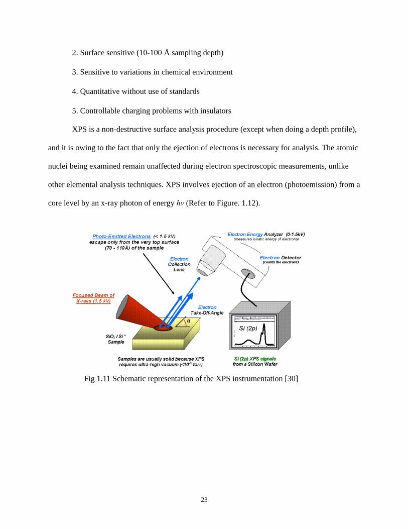
1.6.3 X-Ray photoelectron Spectroscopy (XPS)
1.6.3.1 Introduction and Fundamentals
X-ray photoelectron spectroscopy or electron spectroscopy for chemical analysis (ESCA) is
derived from the photoelectric effect. This is a highly surface sensitive technique useful in the
determination of elemental composition, chemical state analysis, determination of empirical
formula, and determination of the electronic state of a material. Some of the advantages of the
XPS are:
1. Can detect elements from Li up to U
Page 36
23
2. Surface sensitive (10-100 Å sampling depth)
3. Sensitive to variations in chemical environment
4. Quantitative without use of standards
5. Controllable charging problems with insulators
XPS is a non-destructive surface analysis procedure (except when doing a depth profile),
and it is owing to the fact that only the ejection of electrons is necessary for analysis. The atomic
nuclei being examined remain unaffected during electron spectroscopic measurements, unlike
other elemental analysis techniques. XPS involves ejection of an electron (photoemission) from a
core level by an x-ray photon of energy hν (Refer to Figure. 1.12).
Fig 1.11 Schematic representation of the XPS instrumentation [30]
Page 37
24
Conduction Band
Valence Band
Fermi Level
Free electron
Level
Incident x-ray
Photo-emitted
electron
1s
2s
2p
K
L1
L2, L3
Figure 1.12: Schematic diagram of the XPS process, showing photo-electron effect.
As the photoelectrons analyzed eject only from the upper atomic layers of the sample surface
being studied (≤ 100 Å), XPS is a very useful tool for studying interfacial phenomena at the
solid-solid and solid-gas boundaries [31]. Next, electron spectrometer is used to analyze the
emitted photoelectron energy. The electron kinetic energy (EK) is an experimental quantity
measured by the spectrometer, but is not an intrinsic material property as it is dependent on the
incident x-ray photon energy. The electron binding energy (EB) is a parameter which
characterizes the electron, both in terms of its parent element and its atomic energy level. The
relationship between these parameters is:
(Eq. 1.11)
where = work function of the instrument, which is defined as the energy required by the
electron to overcome in order to escape the surface.
Binding energy (EB) represents the strength of interaction between electron (n, l, m, s)
Page 38
25
and nuclear charge. In gaseous medium, EB ~ Ionization potential (IP) (in solids, has to be
added). EB follows energy of levels as: EB (1s) > EB (2s) > EB (2p) > EB (3s), and so on. EB of
orbital increases with the atomic number (z): EB (Na 1s) (z=11) < EB (Mg 1s) (z=12) < EB (Al
1s) (z=13). The reason EB increases with the increase in z, is due to the increase in number of
nucleons attracting the electrons. EB of orbital is not effected by isotopes (e.g. EB of (7Li 1s) = EB
of (6Li 1s)).
Photoelectrons generate x-ray photoelectron spectral peaks, which are termed according to the
orbital (l=0. 1. 2. 3… denoted as s, p, d, f…) and spin (s = ± 1/2) quantum numbers. The total
momentum of the photoelectrons (J = l ± s) is incorporated in the naming of a measured x-ray
photoelectron spectral peak (e.g. Cu2p3/2, where l + s= 1+ ½ = 3/2). The XPS tool is equipped to
measure all the kinetic energy of all the collected electrons, which also includes the contributions
of photoelectron and Auger electron lines. Auger lines result due to ejection of valence level
electrons whose kinetic energy is independent of the photon energy.
Requirements of XPS leading to Photoelectric Effect:
Kinetic energy (EK) of photoelectrons increases as the binding energy (EB) decreases
(from equation 1.11).
Photoemission is directly proportional to the intensity of photons. (more incident photon
will result in more emission of photoelectrons).
Needs a monochromatic (x-ray) incident beam.
A range of kinetic energies can be produced if the valence band is broad.
As each element has their unique set of core levels, kinetic energies can be used to
fingerprint elements.
XPS provides both quantitative and qualitative elemental analysis from a collected spectrum.
Page 39
26
This is accomplished by quantifying the peak intensities which designates an approximate
number of the atoms of a specific element present. The atomic concentration of an element A,
CA, can be calculated by [32]
(Eq. 1.12)
where IA = area of the most intense peak of element A, SA = sensitivity factor, and (In/Sn) = ratio
for all the elements (n) present on the surface. For well-calibrated XPS systems, the precision of
all the quantitative measurements is usually in the range of ±5%.
1.6.3.2 Instrumentation
Modern XPS instruments mainly contain a sample mount system, x-ray source
(monochromator), electrostatic charged-particle energy analyzer, an electron detector enclosed in
an ultra high vacuum (UHV) system, and an optional argon ion gun for sputtering or for
performing a depth profile analysis.
Material of choice for a soft x-ray source should fulfill the following criteria:
1. The line width should not limit the required energy resolution,
2. X-ray energy must be sufficient for the photo-ejection of core electrons for analysis,
3. Suitable x-ray wavelength required to obtain a strong photo-electron signal for analysis.
X-ray anodes usually used in XPS are either magnesium (Mg) or aluminum (Al) with energies
1253.6 and 1486.6 eV [33] which translates to wavelengths of 0.989 and 0.834 nm respectively.
An aluminum source usually produces monochromatic aluminum k-alpha x-rays by focusing and
diffracting a non-monochromatic x-ray beam off of a thin disc of natural, quartz crystal. A 2 μm
thick Al foil has to be inserted between the anode and the sample to protect the sample from
scattered electrons from the anode, heating and contamination effects [34].
Page 40
27
An XPS spectrometer is employed to measure an electron energy spectrum with the help of an
electron energy analyzer. It has the capability to focus and direct the ejected electrons from the
sample surface due to x-ray excitation. A handful of electrons with the desired energy range is
filtered, collected and detected at the detector. The most common analyzers used for XPS
analysis are the double-pass cylindrical mirror analyzer (DPCMA) and the concentric
hemispherical energy analyzer (CHA). CHA is the one more extensively used between the two
and it is made up of two metal hemispheres, one hemisphere is of concave while the other is of
convex shape. They have coincident centers of curvature making the hemispheres concentric. An
electric field is generated in between these two spheres as a consequence of placing varying
voltages on each sphere. The electrons injected into the gap gets attracted to the bottom (positive
applied voltage) and repelled from the top (negative applied voltage). That's why, only selected
electrons having the exact energy (called pass energy) is able to reach the detector.
Detectors that are commonly used in XPS are channeltrons, microchannel plates, and restrictive
anode plates. These detectors amplify each individual electron signals striking the detector
making them detectable. The detector is positioned at the rear of the analyzer slit, and it consists
of several single detectors linked into a computer, to display the plotted spectrum. An ultra high
vacuum (UHV) system (~10-9
torr) is required to detect the low energy electrons emitted from
the surface without any elastic collision. For UHV, the mean free path is very high, of the order
30-40 km).
The XPS measurements were carried forward using a PHI 5000Versa Probe™ Scanning XPS as
shown in Figure 1-13 below. A standard Al-Kα X-ray source was used at 280 watts and
electrostatic analysis in constant pass energy mode of 114.7eV (for survey scans) and 23.5 eV
(for high-resolution scans). This instrument can provide a highly focused monochromatic x-ray
Page 41
28
beam (10-100µm) that can be precisely focused on the area of interest. An optional ion gun
(100V to 5kV differentially pumped Ar ion gun with regulated leak valve with monolayer
resolution) for specimen cleaning and sputter depth profiling is also accessible for use. The Ar
ion gun is also used to neutralize the charging insulating materials during the X-ray irradiation.
In this dissertation, the XPS was utilized to characterize metallic copper, Cu(I) oxide and Cu(II)
oxide while exposing to different chemical environments.
1.6.4 Contact angle measurements
Contact angle (θ) is defined as the angle between the surface of the liquid and the outline of the
contact surface, when an interface exists between a liquid and a solid. The contact angle of a
small, sessile drop, is a function of the surface free energy, and is characterized by the Young-
Dupré equation [35]
(eq. 1.13)
where θ is the contact angle, is the interfacial free energy per unit area, and LV, SV, and SL
Figure 1-13 (a) XPS chamber in (b) PHI 5000VersaProbe™ Scanning XPS
(a) (b)
Page 42
29
refer to liquid-vapor, solid-vapor, and solid-liquid interfaces, respectively. Figure 1.14 presents
an schematic illustration of the parameters used in the Young-Dupré equation.
Figure 1.14 A sessile liquid drop on a solid surface in equilibrium with the vapor phase
The angle of the liquid drop on the solid surface results due to the balance between the cohesive
forces in the liquid and the adhesive forces between the solid and the liquid. As the interaction
increases, the liquid spreads until the angle becomes near 0o. Hydrophobicity and hydrophilicity
of a surface can be determined using water to measure contact angle. In this dissertation contact
angle measurements were utilized in the study of copper corrosion inhibitors to determine the
hydrophobicity of the surface before and after treatment with inhibitors.
1.6.5 Physical vapor deposition (sputtering)
Sputtering is a physical vapor deposition (PVD) process used for material deposition onto a
substrate. Sputtering utilizes a plasma, (typically noble gas ions like Ar+) to knock material off
from a target a few atoms at a time. A general definition of plasma is a set of free charged
particles moving in random paths, which is on average electrically neutral. In sputtering plasma
electrons are more mobile than the large gas ions (Ar+) and are preferentially heated. More
Page 43
30
electrons are lost to the chamber walls due to their high energy and the plasma becomes
positively charged ideally at a constant potential (also known as the plasma potential). The Ar+
ions are then accelerated towards the anode target. After colliding with the target the Ar+ ions
dislodges target atoms, which moves towards the substrate and finally settle on top of it. The
electrons released along with the Argon ionization process are also accelerated towards the anode
substrate, which collides with additional Argon atoms, creating more ions and free electrons in
the process, continuing the cycle.
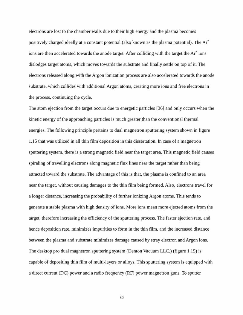
The atom ejection from the target occurs due to energetic particles [36] and only occurs when the
kinetic energy of the approaching particles is much greater than the conventional thermal
energies. The following principle pertains to dual magnetron sputtering system shown in figure
1.15 that was utilized in all thin film deposition in this dissertation. In case of a magnetron
sputtering system, there is a strong magnetic field near the target area. This magnetic field causes
spiraling of travelling electrons along magnetic flux lines near the target rather than being
attracted toward the substrate. The advantage of this is that, the plasma is confined to an area
near the target, without causing damages to the thin film being formed. Also, electrons travel for
a longer distance, increasing the probability of further ionizing Argon atoms. This tends to
generate a stable plasma with high density of ions. More ions mean more ejected atoms from the
target, therefore increasing the efficiency of the sputtering process. The faster ejection rate, and
hence deposition rate, minimizes impurities to form in the thin film, and the increased distance
between the plasma and substrate minimizes damage caused by stray electron and Argon ions.
The desktop pro dual magnetron sputtering system (Denton Vacuum LLC.) (figure 1.15) is
capable of depositing thin film of multi-layers or alloys. This sputtering system is equipped with
a direct current (DC) power and a radio frequency (RF) power magnetron guns. To sputter
Page 44
31
conducting targets, a DC power supply is generally used. For insulating or semiconductor
targets, an RF power supply is required with an automatic or manual impedance matching
network between the power supply and the sputtering gun. The high radio frequency corresponds
to the alternating currents, which allows sputtering of insulating material even in air ambient.
Hence, the magnetic field can be generated on insulating target and sputter-deposit insulating
materials like Si by using RF power source.
1.6.6 Micropattern Corrosion Screening Technique
Micropattern corrosion screening technique is a method that is used to study bimetallic
corrosion as a result of two different metals being in contact. It employs the use of microdots
of ~130 microns diameter and varied thickness depending on experimental need that are
deposited on various substrates through a contact mask using standard magnetron sputtering
machine. The microdots deposited form a micropattern on the substrate of choice to form a
bimetallic contact that can be studied. The samples are then immersed in a corrosive solution
and in situ investigation of corrosion behavior is done by visual inspection using a
Figure 1-15: Dual magnetron gun sputtering system
DC RF
Turbo
pump
Page 45
metallurgical microscope. Figure 1.16 illustrates micropattern corrosion screening structure.
In this dissertation, this novel rapid corrosion screening technique was demonstrated to be
useful in the study of bimetallic corrosion as well as corrosion prevention by inhibitors in
CMP relevant chemical environments.
Figure 1.16: Micropattern Corrosion Screening Technique
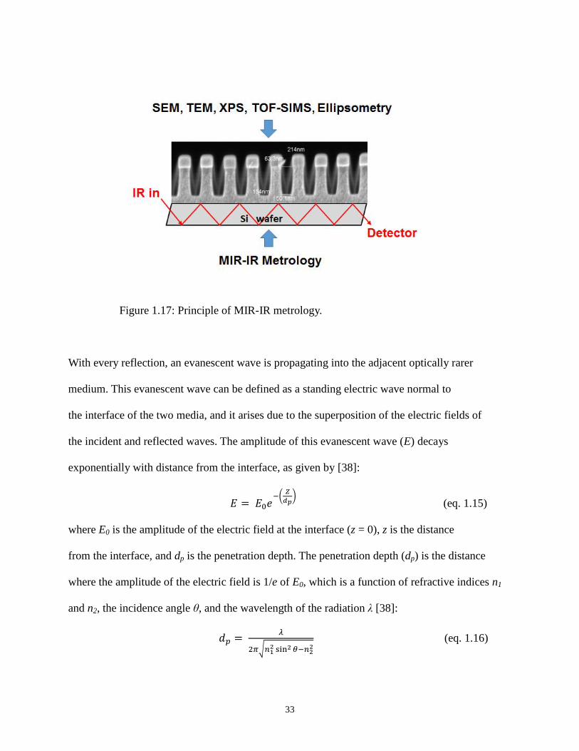
1.6.7 MIR-IR metrology
Multiple internal reflection infrared spectroscopy (or simply MIR-IR) technique is based on
internal reflection spectroscopy, pioneered by Fahrenfort [37] and Harrick [38]. Total internal
reflection occurs at the interface of two media when radiation propagates from the optically
denser medium (refractive index n1) to the optically rarer medium (refractive index n2, n1 > n2),
and the radiation angle of incidence (θ) is greater than the critical angle (θc). The critical angle is
a function of refractive indices of two media and is given by:
(eq. 1.14)
32
Page 46
33
Figure 1.17: Principle of MIR-IR metrology.
With every reflection, an evanescent wave is propagating into the adjacent optically rarer
medium. This evanescent wave can be defined as a standing electric wave normal to
the interface of the two media, and it arises due to the superposition of the electric fields of
the incident and reflected waves. The amplitude of this evanescent wave (E) decays
exponentially with distance from the interface, as given by [38]:
(eq. 1.15)
where E0 is the amplitude of the electric field at the interface (z = 0), z is the distance
from the interface, and dp is the penetration depth. The penetration depth (dp) is the distance
where the amplitude of the electric field is 1/e of E0, which is a function of refractive indices n1
and n2, the incidence angle θ, and the wavelength of the radiation λ [38]:
(eq. 1.16)
Page 47
34
The principle of MIR-IR is shown schematically in figure below:
Figure 1.18: Schematic representation of MIR-IR setup [39]. Optically denser medium has
refractive index n1 whereas optically rarer medium has refractive index n2. Also the radiation
angle of incidence is designated by symbol θ and the critical angle is given by θC.
If the optically rarer medium absorbs IR radiation, attenuated total reflection (ATR) results at
characteristic wavelengths, which corresponds to the vibrational resonant frequency.
1.7 References
1. http://www.intel.com/pressroom/archive/releases/2007/20070128comp.htm
2. G.Moore, “Cramming More Components Onto Integrated Circuits” Electronics, 38, 8
(1985).
Page 48
35
3. Benjamin D. Hatton, Kai Landskron, William J. Hunks, Mark R. Bennett, Donna
Shukaris, Douglas D. Perovic, Geoffrey A. Ozin, “Materials chemistry for low-
k materials” Materialstoday, 9, 3 (2006)
4. S.-P. Jeng, R. H. Havemann, and M.-C. Chang, “Process Integration & Manufacturability
Issues for High Performance Multilevel Interconnect,” M aterials Research Society
Symposium Proceedings: Advanced Metallization for Devices and Circuits-Science,
Technology, and Manufacturability (Pittsburgh, PA: Materials Research Society), 337
(1994)25.
5. S. Wolf, and R.N. Tauber, “Silicon Processing for the VLSI era”, Vol. 1 – Process
Technology, Lattice Press CA (2001)
6. 4. Steigerwald, S.P. Muraraka, and R.J. Gutmann, Chemical Mechanical Planarization of
Microelectronic Materials, John Wiley & Sons (1997).
7. S. P. Murarka, Metallization Theory and Practice fo r VLSI and ULSI, Boston.
Butterworth-Heinemann, 1993,55.
8. P. Shewmon, Diffusion in Solids, second edition, Warrendale, PA: The Minerals, Metals,
and Materials Society, 1989, 224.
9. S. P. Murarka and S. W. Hymes, “Copper Metallization for ULSI and Beyond,” Critical
Reviews in Solid State and M aterials Sciences, 20 (1995) 87.
10. Lee, J. A.; Moinpour, M.; Liou, H. C. ; Abell, T. Proceedings of Materials Research
Soceity, San Francisco, CA, 2003, p. F7.4.
11. Li, Yuzhuo Microelectronics applications of chemical mechanical planarization, John
Wiley and Sons, 2008.
12. http://www.linx-consulting.com/Specialty-abrasives-CMP.html
Page 49
36
13. Zantye, Parshuram B.; Kumar, Ashok; Sikder, A. K. Materials Science and
Engineering R 45, 2004, 89-220.
14. R.J. Guttmann, J.M. Steigerwald, L. You, D.T. Price, J. Nierynck, D.J. Duquette,and S.P.
Murarka, Thin Solid Films, 270, 596 (1995).
15. M. A. Fury, Solid-State Technol., 41, 81 (1997).
16. E. Mendel, Solid-State Technol., 10, 27 (1967).
17. R.G. Kelly, J.R. Scully, D.W. Shoesmith, R.G. Buchheit, Electrochemical Techniques in
Corrosion Science and Engineering, Marcel Dekker, New York, 2003.
18. Steigerwald, J.M., S.P. Murarka, and R.J. Gutmann, Chemical Mechanical Planarization
of Microelectronic Materials. 1997: John Wiley and Sons, Inc.
19. V.R.K. Gorantla, Ph.D. Thesis, Clarkson University (2004).
20. R.K. Singh, A. Zutshi, R. Surana, M. Naik, and T. Pan, MRS Bull., Oct (2002) 776.
21. R. Carpio, J. Farkas, and R. Jairath, Thin Solid Films, 266 (1995) 238.
22. M. Pourbaix, Atlas of Electrochemical Equilibria in Aqueous Solutis, Chapter IV, NACE,
Houston TX (1994).
23. S.V. Babu, K.C. Cadien, and H. Yano, Eds., Chemical Mechanical Polishing-Advances
and Future Challenges, Mat. Res. Soc. Symp. Proc. 671 (2001).
24. S. Balakumar, T. Haque, R. Kumar, A.S. Kumar, and M. Rahman, Mat. Res. Soc. Symp.
Proc. 867 (2005).
25. http://nptel.ac.in/courses/113108051/module1/lecture5.pdf.
26. M. Pourbaix, Thermodynamics of Dilute Aqueous Solutions, London: Edward Arnold,
1949, 54.
Page 50
37
27. B. Beverskog and I. Puigdomenech, “ Revised Pourbaix Diagrams for Copper at 25 to
300°C,” Journal of the Electrochemical Society, 144 (1997) 3476.
28. L. R. Faulkner, J. Chem. Ed,. 60, 262, (1983).
29. D. D. MacDonald, Electrochim. Acta, 51, 1376 (2006).
30. https://en.wikipedia.org/wiki/X-ray_photoelectron_spectroscopy
31. C. C. Chusuei, D. W. Goodman, Encyclopedia of Physical Science and Technology, 3rd
Edition, Vol. 17, Academic Press (2002).
32. S. Nasrazadani, I. Fritsch, C. S. Henry, “Analytical Techniques for Materials
Characterization.” In Advanced Electronic Packaging, edited by W.D. Brown, New York,
1999.
33. C. R. Brundle, “X-Ray Photoelectron Spectroscopy” In Encyclopedia of Materials
Characterization, edited by Brundle, C. R., Evans, C. A. Jr, Wilson, S., Massachusetts,
Butterworth-Heinemann, 1992.
34. H. Bubert, J. C. Rivière, “Photoelectron Spectroscopy” In Surface and Thin Film
Analysis: A Compendium of Principles, Instrumentation, and applications, edited by
Bubert, H., Jenett, H., Federal Republic of Germany, Wiley-VCH, 2002.
35. T. S. Chow (1998). "Wetting of rough surfaces". Journal of Physics: Condensed Matter
10 (27): L445
36. R. Behrisch, “Sputtering by Particle bombardment”. Springer, Berlin, (1981).
37. J. Fahrenfort. Attenuated total reflection. A new principle for the production of useful
infrared reflection spectra of organic compounds, Spectrochim. Acta 1961, 17, 698-709.
38. N. J. Harrick. “Internal Reflection Spectroscopy”, John Wiley & Sons, Inc.: New York,
1967.
Page 51
38
39. B. Mizaikoff. “Waveguide-enhanced mid-infrared chem/bio sensors”, Chem. Soc. Rev.,
2013, 42, 8683-8699.
Page 52
39
CHAPTER 2
STUDY OF PYRAZOLE AS COPPER CORROSION INHIBITOR
IN MODEL ALKALINE POST CHEMICAL MECHANICAL POLISHING
CLEANING SOLUTION
2.1 Introduction
At the turn of the millennium, copper has replaced aluminum as the interconnect material
in Ultra-large-scale integration (ULSI) devices due to its high electromigration resistance and
low electrical resistance [1-2]. Despite substantial reduction in resistance-capacitance (RC)
delay, several challenges were encountered in the integration of copper as wiring metal. One of
the major challenges is, conventional technique like etching process cannot be applied for copper
patterning due to lack of copper compound with high enough vapor pressure at relatively low
temperature [3]. A more pragmatic approach to the Cu integration process involves deposition of
a diffusion barrier (Ru, Ta, TaN) and Cu metal into interlayer dielectrics (ILD), known as
Damascene process, followed by removal of overburden metals by chemical mechanical
polishing (CMP) technique [4-5]. Damascene technology is defined as the processes of forming
trenches filled with interconnect (copper) and then planarizing it in such a way that allows
copper to remain only in the trenches. CMP essentially involves polishing of wafers against a
pad under pressure using slurry consisting of abrasive particles and various chemicals. The
overburden material is removed from the wafer surface due to the synergistic effects of the
Page 53
40
chemical reactions (between the material being polished and chemicals in the slurry) and the
mechanical action due to abrasives. The introduction of copper in semiconductor devices has
brought attention to the phenomena of thin film corrosion that must be minimized for optimal
device performance, reliability, and longevity. Since CMP and post CMP cleaning processes are
inherently wet processes, they expose Cu interconnect and barrier to the corrosive chemicals
relevant to these processes. This results in bimetallic corrosion that can be detrimental to the
yield and reliability of integrated circuits devices. Furthermore, CMP process leaves Cu residues,
organic residues, abrasive particles and other contaminants on the surface that can degrade the
electrical properties of ILDs, lower the conductivity of Cu and lead to poor adhesion of the
subsequent layers [6].
To avoid reliability issues, an effective post CMP cleaning step is therefore required to
remove the residues and contaminants. Both acidic and alkaline cleaning solutions have been
developed in recent years that effectively remove Cu residues and contaminants. Recent study
has shown alkaline post CMP cleaning solution to be more effective to achieve a good cleaning
performance and low surface roughness [7]. One of the advantages of alkaline cleaning
chemistry is the selective dissolution of CuO at high pH, leaving Cu2O passivating layer on Cu
surface. Also at high pH conditions, the negative zeta potential (NZP) aids in keeping the
removed particles in the solution and does not allow them to reattach to the wafer surface or
brush PVA [8]. Alkaline post CMP cleaning solution used for this study is called Tetra methyl
ammonium hydroxide (TMAH), a very strong base (with a pKb ~ 0). Unlike ammonia, it does
not form complexes with copper. TMAH solutions can also be obtained in very high purity with
minimal ionic contamination. TMAH has been used in proprietary chemicals for effective
inhibition and prevention of re-adhesion of particles that are removed during the cleaning
Page 54
41
process [9]. Although the TMAH based solution is efficient in removing the residues and
contaminants, it has been documented to be corrosive towards Cu and could therefore cause
serious reliability issues [9]. This is a significant drawback as the Cu/diffusion barrier contacts
are inevitably exposed to the corrosive chemicals used during the cleaning process. Ruthenium
(Ru) has been explored as alternative barrier/liner materials to replace tantalum/tantalum nitride
(Ta/TaN) bilayer stack because of the scaling difficulty [10-12]. However, Cu/Ru bimetallic
corrosion could be of concern since Ru belongs to the platinum group metals that is more noble
than Cu. Previously, we reported a novel bimetallic corrosion testing technique, which is an
effective methodology for evaluating bimetallic corrosion of Cu interconnects when exposed to
CMP and post CMP cleaning conditions and showed that Cu/Ru exhibit enhanced corrosion
compared to Cu/Ta [13]. Micropattern corrosion testing technique has the advantage of allowing
actual monitoring of corrosion of Cu when in contact with a barrier metal unlike other methods
hence the bimetallic effect can be evaluated.
Reliable Cu metallization process is achieved when metal loss is minimized during post
CMP cleaning and is achieved by addition of a corrosion inhibitor into the cleaning solution.
Significant progress had been made in the study of copper corrosion inhibitors and nitrogen
heterocycles have been found to be effective metal corrosion inhibitors. This is because of their
chelating action and formation of physical barrier on the surface of the metal that prevent
corrosion [14]. Among them, benzotriazole (BTA) has been extensively investigated and used as
Cu corrosion inhibitor in both acidic and alkaline post CMP cleaning solutions [15-18]. Neutral
BTA exists in two tautomeric forms in equilibrium – 1 H-benzotriazole and 2 H-benzotriazole,
where the former is the predominant species (99.9%) in both solution and gas phases. Due to the
presence of multiple electronegative nitrogen atoms in the ring, BTA has appreciable NH
Page 55
42
acidicity (pKa ~8.2) and at high pH conditions, mostly exists in its highly resonance stabilized
conjugate base form, benzotriazolyl anion. BTA has been widely used as metal corrosion
inhibitor due to its strong metal-chelating capability and presence of hydrophobic benzene ring
(water solubility is 1.8-2.5 wt%). BTA physisorption at the metal interface, formation of BTA-
metal complexation monolayer and subsequent molecular self assembly via strong π-π
interaction between BTA aromatic rings combine to result a hydrophobic protective film, ([Cu+
BTA-]n), on the metal surface rendering it inaccessible for any attack from corroding chemicals
[19-21]. Inhibition efficiency of BTA for Cu corrosion is a function of the temperature,
concentration of BTA, immersion time, oxidation states on Cu surface and the pH. BTA
adsorption is much faster on Cu2O layer than on CuO or pristine Cu surface and therefore
thickness of Cu2O underlayer determines thickness of the Cu-BTA protective layer. The
adsorption of BTA on an oxide-free Cu surface, which is the case in very high pH conditions, is
suggested to be improbable or minimal [22]. According to Pourbaix diagram, at higher pH, Cu
surface comprises less oxide layer and mostly exists in Cu0 state and at pH approaching 14, Cu
directly transforms into CuO22-
ion [23]. Moreover, due to its poor aqueous solubility and
inherent hydrophobicity, BTA contributes to increased organic residue defects on water surface
and therefore not efficient when used as Cu corrosion inhibitor in aqueous alkaline post CMP
cleaning solution. Therefore, BTA needs to be replaced by an efficient corrosion inhibitor that is
effective in highly alkaline (> pH 12) post CMP cleaning formulations and the treated surface is
more hydrophilic in nature.
One of the potential substitutes is Pyrazole which is readily water soluble unlike BTA. It is a
weaker NH acid (pKa ~14.21) than BTA partly due to dimer formation via intermolecular
hydrogen bonding. The conjugate base, azolyl anion, is stabilized by two equally contributing
Page 56
43
resonance forms [24]. The inhibition effect of Pyrazole and Pyrazole derivatives on the corrosion
of Cu has been studied in hydrochloric acid using impedance spectroscopy and polarization
methods [25-26]. It was found that inhibitors adsorbed on Cu surface to form Pyrazole-Cu (II)
complex protective layer without changing Cu dissolution mechanism. Research of Pyrazole as
Cu corrosion inhibitor has largely been done in acidic solutions and very little in alkaline
solutions [27] using electrochemical methods. Figure 1 shows molecular structure of BTA.
In this study, we report the effectiveness of an Pyrazole compound in the inhibition of Cu
corrosion in 8 wt.% TMAH (pH 14) solution and compare it to BTA under the same conditions.
The investigation was carried out in-situ using the micropattern corrosion screening technique.
Corrosion potentials and currents measured by electrochemical technique, and XPS analyses
complemented well with micropattern corrosion screening results to demonstrate efficiency of
Pyrazole in Cu corrosion inhibition in TMAH based alkaline post CMP cleaning solution.
Figure 2.1 Structure of (a) benzotriazole (BTA) and (b) pyrazole
2.2 Literature survey of inhibitor performance
2.2.1 The structure of copper-azole complexes
Azoles are organic compounds containing nitrogen atoms with free electron pairs that are
1
2
3
Page 57
44
potential sites for bonding with copper and that enable inhibiting action. Various studies of the
structure of the Cu(I) [1] and Cu(II) [29–34] azole complexes concluded that the bonding occurs
through the N atoms. Other heteroatoms like sulphur, if present along with nitrogen, can also
participate in bonding [35,36], and that the coordination number can be as high as four. As these
azole ligands are planar, they impose a planar structure on the resultant coordination complexes.
However, in some cases complex could not exist in a coplanar form due to the steric hindrance
that can be avoided by plane rotation of some of the ligands [28,30–34]. On the other hand,
presence of any significant amount of single bond–double bond resonance in the Cu–N bond,
tends to stabilize the completely planar configuration [32]. Steric hindrance can give rise to a
negative interaction among the ligands that can introduce porosity to the complexes [28].
However, the crystal structure may further be stabilized by intramolecular and intermolecular
hydrogen bonds [30]. Another characteristic of azole compounds is observed and that is their
ability to act as polydentate ligands [30-32].
2.2.2 Benzotriazole
The most commonly used copper corrosion inhibitor of azole type is Benzotriazole
(BTA). BTA consists of benzene and triazole ring. BTA can exist in three forms depending on pH
value of the solution. In strongly acidic media it has protonated form BTAH2+, in weakly acidic,
neutral and weakly alkaline media its form is BTA, while in strongly alkaline media it is BTA-
[37]. According to the E–pH diagrams for systems containing Cu and BTA [38], it is possible to
predict whether the inhibiting action can be expected. The same is confirmed by the results of
Hope et al. [39] who observed that the adsorption of BTA onto the copper surface was reversible
at pH levels below 3, and depends upon both solution pH and the applied electrode potential. At
Page 58
45
lower pH the coordination between Cu and BTA as well as the chemisorption of BTAH2+ onto
the electrode surface occur, whereas at higher pH levels the surface layer [Cu(I)–BTA] was
observed on the electrode. Dugdale and Cotton [40] observed that benzotriazole, unlike the
inhibitors that act only through adsorption, can form chemical bond to the metal or metal oxide
surface. Thus, once the metal surface has been pre-treated, the effect is long-lasting and does not
require renewal. Electrochemical measurement has indicated that corrosion inhibition by
benzotriazole does not result solely from the blocking action of the copper–benzotriazole
complex.
Generally about BTA action it can be said that it is anodic copper corrosion inhibitor
which action mechanism includes chemisorption, rearly physisorption on the copper surface that
follows Langmuire isotherm followed by the formation of complex Cu(I)BTA. Coordination
between BTA molecule and Cu electrode surface occurs via nitrogen atom of triazole ring. BTA
molecules can be oriented parallel or vertical regarding surface. The orientation of inhibitor
molecule is important because of the possibility of formation of stronger bond if the orientation
is parallel due to interaction of p electrons of the ring with vacant d orbitals of copper. [41]
According to Tromans and Sun [37], BTA can react with the clean copper surface to form the
protective film. The study of Xue et al. [42] conducted on the clean copper surface proved that
adsorbed BTA anchored directly to the metal. The metallic copper reacts with BTA at a faster
rate providing much better corrosion protection than the oxidized surface. It is proposed that the
surface moiety is [Cu(I)–BTA-] and the isolated product is [Cu(II)–(BTA
-)2]. Hence, BTA can
react with copper metal at zero oxidation state under mild conditions to form
(benzotriazolato)copper(1+) according to the following mechanism. In neutral solutions, BTA
functions as a ligand by means of the unshared pair of electrons on the ‘‘pyridine”-type nitrogen
Page 59
46
(N2). The first step of the reaction is the formation of a [Cu(0)–BTA] complex by ligation of
pyridine nitrogen of BTA with metallic copper. In [Cu(0)–BTA] complex, both the copper atom
and the imino group are activated. On the other hand, as the solution is exposed to air, copper
metal can adsorb oxygen from solution, to form adsorbed oxygen species, eg, undissociated
dioxygen, O2.
It has been reported that the coadsorbed oxygen shows more basic and oxidizing properties than
the oxygen in air or in solution. So, under mild conditions, copper metal is prone to donate
electrons and BTA can be deprotonated, resulting in the formation of the complex
(benzotriazolato)copper(1+) and water. Two of the nitrogen atoms in the benzotriazolium anion
are indistinguishable and are equivalent for coordination. Each cuprous cation coordinates with
two nitrogen ligands. It is reasonable to propose the structure of (benzotriazolato)copper(l+) to
be that of an infinite polymer with the benzotriazolium anions acting as bridging ligands. The
third nitrogen atom in the anion can also ligand to copper surface, forming a polymeric
protecting layer.
2.2.3 Pyrazole
The inhibiting effect of pyrazole (Pz) on Cu anodic dissolution in 0.1 M HCl was
investigated by Geler and co-workers [43]. Based upon the experimental results, the inhibition
effect of Pz can be related to an adsorption process which takes place through the lone-pair of
electrons of the azole nitrogen and/or the six delocalized p-electrons of the pyrazole ring.
Furthermore the presence of pyrazole changes the mechanism of copper dissolution in chloride
media, by decreasing the rate of cuprous species formed and increasing that of the cupric species.
The action of pyrazole can be physically interpreted as blockage of the metal surface by copper–
Page 60
47
pyrazole species produced during the anodic sweep, however, they are poorly adhered to the
electrode surface. It is suggested that the use of Pz derivatives with higher electron density would
favour the formation of strongly bound complexes. The same is confirmed in the study
conducted by Vera et al. [44], where the ability of the tetradentate 1,5-bis(4-dithiocarboxylate-1-
dodecyl-5-hydroxy-3-methylpyrazolyl)pentane, BDTCPP to inhibit copper corrosion in 3.5%
NaCl solution is investigated. The inhibitor prevents copper corrosion by physisorption on the
metal surface, followed by chemisorption of a protective Cu(II)-complex. BDTCPP acts as a
tetradentate ligand to form a 1:1 [Cu(II)–BDTCPP] square–planar complex. The layer covers the
substrate completely, making the surface more smooth and homogeneous, without bare copper
exposed to the electrolyte. The high inhibition efficiency can be attributed to the good adherence
of the complex on the copper surface. These properties can be related to the structural
characteristics of the BDTCPP ligand: planar with high p/lone-pair electron density conjugate
heterocyclic 4-dithiocarboxylate-5-hydroxy pyrazolyl moiety, with nitrogen and sulphur atoms
having high affinity for copper atoms.
2.3 Experimental Procedure
Corrosion measurement in this study was done by micropattern corrosion testing
technique described elsewhere [13]. As demonstrated in figure 2, copper microdots (ca. 50 nm
thick, 130 µm in diameter pattern transferred via contact mask on to Ru, Ta and glass substrates)
as well as Ru and Ta substrates on Si were deposited using magnetron sputtering (Desktop Pro,
Denton Vacuum). The actual corrosion process of micropattern array is recorded using an optical
microscope (Nikon, Eclipse ME600). The corrosion rate (Å/min) can be estimated by the time of
complete disappearance of Cu dots after immersion in the probing chemical solution. Bimetallic
Page 61
48
corrosion screening technique has the advantage of allowing the direct observation of corrosion
of a metal in direct contact with another metal hence the effect of bimetallic contact can be
determined instantly under different conditions. It is also a fast corrosion screening technique as
Cu microdots were designed to be thin enough to permit screening many corrosion inhibitors
within a short period of time.
Figure 2.2 Micropattern corrosion screening structure
Pyrazole (98% Sigma-Aldrich), BTA (97% Sigma-Aldrich), and TMAH (25 wt.% Sigma-
Aldrich) were used as received. Model aqueous cleaning solution containing 8 wt.% TMAH (pH
14) in water, as a representative of mainstream proprietary alkaline cleaning solution was
prepared using pre-purified water (>18.2 MΩ, Millipore integral 3) [6,45]. All electrochemical
measurements were done using CHI 760D (CH Instruments) potentiostat. Cu shot, 5mm in
diameter was used as the working electrode. The metal electrode was polished down to 0.5
micron mirror polishing and sonicated in de-ionized water. A three-electrode system with Pt as
the counter electrode and Ag/AgCl as reference electrode was used in an electrochemical cell.
Electrochemical impedance spectroscopy (EIS) measurements were completed by superimposing
an ac signal with amplitude of 5 mV peak to peak and frequency range from 100 kHz to 50 mHz.
Page 62
49
The EIS results were analyzed using ZSimpWin software.
XPS samples were prepared by sputter depositing Cu on Ru substrate (1cm2) and
immersing them in 8 wt.% TMAH solution containing 1mM Pyrazole and 10mM BTA for 20
minutes. The samples were rinsed with de-ionized water and blow-dried with dry nitrogen purge.
XPS analyses were conducted ex-situ using a PHI 5000 VersaProbe, a multi-technique surface
analyses instrument equipped with Al Kα (1486.7 eV) radiation and dual-gun charge
compensation system for analysis of all sample types.
2.4 Results and Discussion
2.4.1 Effect of Substrate on Cu Corrosion
The nature of bimetallic contact was studied to determine the effect on the rate of Cu
corrosion. Figure 3a shows the time-lapsed images of Cu micropatterns on three different
substrates; Ru, Ta and glass submerged in the alkaline TMAH (8 wt.%, pH=14). Ta is currently
used as part of the diffusion barrier for Cu interconnects in integrated circuit devices [46-47]
while Ru is a new promising candidate for liner metal because Cu can be directly plated onto Ru
without Cu seed [48-49]. Glass was chosen as a non-conductive dielectric substrate. As shown in
Figure 3, Cu microdots on Ta substrate required over 4X the amount of time as compared to Cu
microdots on Ru substrate to corrode completely in TMAH pH=14 solution. Based on the
micropattern screening, the Cu corrosion trend follows Cu/Ru (27 min) > Cu/Glass (56 min) >
Cu/Ta (120 min).
Tantalum has a strong tendency to be oxidized and form tantalum oxide (Ta2O5) especially when
exposed to aqueous medium, Eq. 1.
2Ta + 5H2O = Ta2O5 + 10H+ + 10e
- ------ (1)
Page 63
50
Ta exhibits a thermodynamically favorable oxidation reaction that donates electrons through the
Cu/Ta bimetallic contact. This results in cathodic protection of Cu microdots. On the other hand,
Ru is nobler than Cu therefore Cu oxidation is facilitated through Cu/Ru bimetallic couple. Cu
microdots on glass was used to represent Cu only corrosion case and as expected it exhibited a
corrosion rate that is in between Cu/Ru and Cu/Ta [13].
Figure 2.3 Time lapsed images of Cu microdots deposited on Ru, Ta and glass in 8 wt.% TMAH
solution
To confirm the trend of galvanic corrosion, Tafel plots (figure 2.4) were recorded for Cu,
Ru and Ta in TMAH pH 14 solution. The corrosion potentials mostly followed a general trend of
Ecorr, Ru > Ecorr, Cu > Ecorr, Ta which correlated well with the expected metal nobility trend.
Page 64
51
Figure 2.4 Tafel plots of Ru, Cu and Ta measured in TMAH pH 14 solution
2.4.2 Cu Micropattern Corrosion and Inhibition
Chemical composition of post CMP cleaning solution has a direct effect on bimetallic Cu
corrosion process. The continued shrinking of Cu interconnects features in order to satisfy
Moore's law has led to increased need to minimize Cu corrosion during post CMP cleaning to an
industrially accepted rate of <1Å /min. The Pourbaix potential-pH diagram indicates that
alkaline solution condition could facilitate Cu to corrode more readily. Cu bimetallic contact with
Ru leads to accelerated corrosion which was confirmed using micropattern corrosion screening
technique. The nobility of Ru in TMAH solution and with addition of Pyrazole and BTA was
determined using Tafel plots. The icorr and Ecorr were found to have negligible difference for the
three plots therefore confirming that Ru in TMAH is not affected by the presence of corrosion
inhibitors .The proposed mechanism of Cu/Ru corrosion is shown below.
Page 65
52
Ru cathode
)(442 22 ORROHeOHO Slow Oxygen reduction reaction
Cu anode
2
2
2
2
2
22
)(
222
2222
OHCuOHCu
eOHCuHOCu
eHOCuOHCu
Slow
Figure 2.5 shows corrosion rate of Cu microdots on Ru in 8 wt.% TMAH with respect to
increasing concentrations of Pyrazole and BTA. Figure 2.6 displays the time lapsed images of Cu
microdots after immersion in the same TMAH solution and with 10mM BTA and 1mM Pyrazole.
The time required to completely erode 50nm Cu dots can be used to gauge the relative rate of
corrosion. The corrosion rate can therefore be estimated to be inversely proportional to corrosion
time. The relative Cu corrosion rate of Cu/Ru micropattern in 8 wt.% TMAH (27Å /min) only
partially diminished after addition of up to 10mM BTA (8Å /min). Comparatively, Cu corrosion
rate of Cu/Ru micropattern was significantly reduced (<1Å /min) after addition of 1mM Pyrazole
in 8 wt.% TMAH solution. Further increase in Pyrazole concentration did not result any
substantial corrosion rate decrease. From the results, we conclude that 1mM Pyrazole is needed
to achieve the industry acceptable Cu corrosion rate of <1Å /min. Furthermore, it is desirable to
keep the inhibitor concentration very low because the excess inhibitor on Cu surface becomes the
source of organic contamination that can affect the conductivity and interlayer adhesion of the
subsequent layers. This demonstrates that Pyrazole is a better candidate for Cu corrosion
inhibition in highly alkaline TMAH solution as compared to the industrial standard, BTA. All
subsequent experiments in this paper were carried out using 1mM Pyrazole and 10 mM BTA.
Page 66
53
Figure 2.5 Inhibitor concentration dependent etch rate of Cu in 8 wt.% TMAH
Figure 2.6 Time lapsed images of 50nM Cu/Ru immersed in 8 wt.% TMAH with additional
1mM Pyrazole and 10mM BTA
Page 67
54
2.4.3 Electrochemical Analysis
2.4.3.1 Tafel Plots
The trend of Cu corrosion was also monitored using Tafel plots. The rate of corrosion can
be theoretically calculated from corrosion current which is obtained from extrapolation of anodic
and cathodic curves. As shown in Figure 2.7, the corrosion current follow the trend of icorr, no
inhibitor> icorr, 10mM BTA > icorr. 1mM Pyrazole which correlated well with the results from micropattern
corrosion screening while the Ecorr remain relatively the same. The disadvantage of Tafel plot
method is that the corrosion rate is obtained from fresh electrode/solution and the study is limited
to short term study only. Furthermore, corrosion study by Tafel plots is based on a single metal
electrode and cannot be directly applied to bimetallic corrosion which are both addressed by
micropattern screening technique.
Figure 2.7 Tafel plots of Cu in 8wt.% TMAH and with Pyrazole and BTA
Page 68
55
2.4.3.2 Electrochemical Impedance Spectroscopy (EIS)
EIS is an effective technique that is used in the analysis of various steps involved in an
electrochemical reaction by measuring the response of impedance system to a small ac potential
in a wide frequency range [50]. It provides a method for measuring the resistance against the
transfer of ionic species to the metal surface and has been used to evaluate the barrier properties
of corrosion inhibitors [51-52]. Corrosion of Cu in 8 wt.% TMAH solution in the presence of
BTA and Pyrazole inhibitors was investigated by EIS to substantiate the aforementioned
effectiveness of Pyrazole as Cu corrosion inhibitor. The results of the successive impedance
scans are shown in figure 2.8 in the form of Nyquist plots. All the impedance data were fitted
using an equivalent circuit shown in figure 2.8 (inset) where Rs represents the solution resistance,
Rdl is the charge transfer resistance, Qdl is double layer constant phase element (CPE), Rf is layer
resistance and Qf (CPE) represent the protective properties of the film on Cu. This equivalent
circuit has been used to fit impedance data in studies of corrosion inhibition by organic coatings
[51, 53-54].
As seen in the Nyquist plot (figure 2.8), addition of BTA and Pyrazole increases the charge
transfer resistance of the Cu electrode in TMAH solution. This is arrived at by evaluating the
diameter of the semicircular Nyquist plots which clearly increases with the addition of BTA and
Pyrazole to TMAH. The increase in charge transfer resistance could be due to the adsorption of
inhibitor molecules on the Cu surface which modifies the surface by decreasing the electrical
capacity because of displacement of water molecules and other ions originally adsorbed on the
surface. It is particularly important to note that the charge transfer resistance with addition of
Pyrazole is ~ 10X higher than that of the TMAH solution contains BTA. This confirms the
Page 69
56
formation of a denser protective layer on the surface of Cu by pyrazole compared to the one
formed by benzotriazole which explains why Pyrazole exhibited effective corrosion inhibition
shown by Micropattern corrosion screening.
Figure 2.8 EIS data (a) Nyquist plot of Cu in TMAH (black), TMAH +BTA (red) and
TMAH+Pyrazole (blue) and inset equivalent circuit used to fit data.
2.4.4 Water Contact Angle Measurement
Surface tension or wettability of Cu surface is an important aspect in post CMP cleaning.
It has direct impact on the cleaning results as a hydrophilic surface enables relatively easy
flushing away contaminants and minimizes watermarks [55]. Cu samples were submerged in
TMAH solution and TMAH with 1mM Pyrazole and different concentrations of BTA for 20
minutes followed by DI water rinse and air-dry and subsequent contact angle measurement on
the treated surfaces. As shown in Figure 2.9, significant differences of wettability of Cu were
Page 70
57
observed among the test solutions. The TMAH solution containing BTA produced hydrophobic
surface and hydrophobicity increased with concentration. Surface hydrophobicity of
BTA/TMAH-treated Cu surface is commonly attributed to the specific orientation of BTA
molecules relative to the Cu surface where hydrophobic benzene ring is facing away from Cu
surface and therefore forming a protective hydrophobic barrier [56]. The TMAH solution
containing Pyrazole produced a relatively hydrophilic Cu surface after immersion compared to
the ones treated with BTA/TMAH solution. This is likely due to relatively smaller size of
Pyrazole molecule owing to the absence of large hyrdrophobic benzene moiety. As a result, a thin
hydrophilic Cu-Pyrazole complex is adsorbed Cu surface.
Figure 2.9 Variation in DI water contact angle of Cu in TMAH and TMAH+ inhibitor
Page 71
58
2.4.5 Surface Analysis
2.4.5.1 XPS Analysis
XPS analysis was done on three substrates; bare Cu, Cu immersed for 20 minutes in
TMAH with 10mM BTA and TMAH with 1mM Pyrazole. Figure 2.10 present the spectra of Cu
2p and auger spectra (Cu LMM). From the results, it is clear the chemical surface states are
different for the three substrates. Bare Cu contains CuO and CuOH which is indicated by Cu
2p3/2 at 933.8 eV and Cu LMM at 569.4 eV (Figure 2.10a and b).The intense shake up satellites
around 938-946 eV indicates the presence of Cu2+
which is evoked by the availability of unfilled
d-orbitals (d9) [57-59]. The peak at 932.5 eV is attributed to either Cu2O or metallic Cu. The
difference in energy between Cu2O and Cu is about 0.1eV [60] and it was difficult to distinguish
the two with the resolution of our instrument. CuLMM spectra on the other hand has a difference
of about 2.6 eV between Cu2O (570.5 eV) and Cu (567.8 eV). This is as a result of the relaxation
energy difference between the materials [61]. In bare Cu analysis, Cu2O is not present because of
the absence of the characteristic CuLMM peak at 570.5 eV.
The Cu 2p3/2 component of Cu immersed in TMAH solution with 10mM BTA (Figure
2.10c) shows a sharp peak at 932.5 eV which is attributed to Cu2O or metallic Cu. This is
confirmed by the CuLMM peak at 570.5 eV (Figure 2.10d) which is typical of Cu2O. This indicates
that a protective film is present on Cu surface, but protection is not effective based on
micropattern corrosion screening results. Cu substrate immersed in TMAH solution containing
1mM Pyrazole showed a sharp peak on Cu 2p spectra at 932.5 eV (Figure 2.10e). The actual
identification was confirmed by CuLMM spectra with 2 peaks, the main peak at 567.8 eV (Figure
2.10f) that is typical metallic Cu and another peak at 570.5 eV that is Cu2O [62-63]. This reveals
the absence of Cu2+
on the substrate treated with Pyrazole and could be as a result of formation
Page 72
59
of Cu(1)-Pyrazole complex on Cu surface. The presence of the Cu2O on the surface after
treatment with Pyrazole may suggest the adsorption process involves oxidation of Cu atoms to
Cu+ followed by chemisorption of the inhibitors.
Figure 2.10 XPS Cu 2p spectra of; (a) bare Cu, (b) BTA modified Cu and (c) Pyrazole modified
Cu and Cu LMM spectra of; (d) bare Cu, (e) BTA modified Cu and (f) Pyrazole modified Cu
Figure 2.11 is the N1s spectra of three Cu substrates. As expected, bare Cu (Figure
2.11a) depicts absence of N1s peak. The substrate containing BTA in TMAH (Figure 2.11b) has a
single and significantly narrower peak located at 400.2 eV. The narrower N1s peak indicates that
the charge is evenly distributed by the conjugated π structure delocalized over the two N atoms
and both N1 and N3 are equivalent [64-65]. This could signify absence of Cu-N bonding and
Page 73
60
explanation of ineffective corrosion inhibition as depicted by micropattern corrosion screening.
The sample treated with Pyrazole (Figure 2.11c) has two peaks; one at 400.2 eV and the other
one at 399.6 eV. This shows that the two N atoms are not equivalent which may indicate that one
of the N atoms in Pyrazole molecule is bonded to Cu(1) or Cu as bonding changes the electron
environment of one N atom compared to the second one [64]. This therefore demonstrates that
the effectiveness of Pyrazole in inhibition of Cu corrosion is through formation of Cu-Pyrazole
complex to form the inhibition film.
Figure 2.11 XPS N1s spectra of: (a) bare Cu, (b) BTA modified Cu and (c) Pyrazole modified
Cu
2.5 Proposed Mechanism of Cu Corrosion Inhibition
Based on the data obtained we propose a mechanism of Cu corrosion inhibition in TMAH
Page 74
61
solution by Pyrazole. This involves first ionization of Pyrazole (Pz) in highly alkaline (pH 14)
TMAH solution as shown in the following equation
Pz-H → Pz- + H
+
Pz- then reacts with Cu
+ metal center from surface oxide layer to form Cu(1)-Pz complex
Cu+ + Pz
- → Cu(1)-Pz
The dissolution of Cu in 8 wt.% TMAH is therefore hindered by the strongly adsorbed protecting
layer of Cu(1)-Pz complex by favorable Pz-H ionization promoted by strongly alkaline TMAH
solution environment. The Cu(1)-Pz complex formed on the surface creates a physical barrier
that prevents further contact of Cu with TMAH and hence prevents Cu corrosion.
2.6 Summary
In this study, Pyrazole was demonstrated using various experimental methods to be an
effective Cu corrosion inhibitor compared to BTA in alkaline post CMP cleaning solution
containing TMAH. 1mM of Pyrazole showed effective inhibition of Cu corrosion while BTA up
to 10mM resulted in Cu Corrosion. From the XPS and ATR-IR analysis it was depicted that
Pyrazole inhibit Cu corrosion in TMAH by the formation of Cu-Pyrazole complex. The
reproducible micropattern corrosion screening confirmed that Pyrazole is more effective
corrosion inhibitor that BTA in TMAH solution.
2.7 References
1. A. Sethuraman, J.-F. Wang, and L. M. Cook, J. Electron. Mater., 25, 1617 (1996).
2. T. J. Licata, E. G. Colgan, J. M. E. Harper, and S. E. Luce, IBM J. Res. Dev., 39, 419
(1995).
Page 75
62
3. J. Steigerwald, M. Zirpoli, S. P. Murarka, D. Price, and R. J. Gutmann, J. Electrochem.
Soc., 141, 2842, (1994).
4. K. W. Chen, Y. L. Wang, L. Chang, S. C. Chang, F. Y. Li, and S. H. Lin, Electrochem.
Solid-State Lett., 7, G238 (2004).
5. A. Jindal and S. V. Babu, J. Electrochem. Soc., 151, G709 (2004).
6. L. Zhang, S. Raghavan, and M. Weling, J. Vac. Sci. Technol. B, 17, 2248 (1999).
7. A. Ouerd , H. Dulphy , V. Lelievre, L. D. Cioccio, and M. Rivoire, International
Conference on Planarization/CMP Technology, 15 (2012).
8. R. Prasanna Venkatesh, T.-Y. Kwon, Y. Nagendra Prasad, S. Ramanathan, and J.-G. Park,
Microelectron. Eng., 102, 74 (2013).
9. M. Fischer, US20070225186 A1 (2006).
10. T. N. Arunagiri, Y. Zhang, O. Chyan, M. El-Bouanani, M. J. Kim, K. H. Chen, C. T. Wu,
and L. C. Chen, Appl. Phys. Lett., 86, 083104 (2005).
11. K. Mahadevaiyer, J. W. Nalaskowski, and L. M. Cook, Chem. Rev., 110, 178 (2010).
12. S.-C. Seo, C.-C. Yang, C.-K. Hu, A. Kreber, S. Fan, D. Horak, D. Canaperi, S. Papa Rao,
B. Haran, and B. Doris, Electrochem. Solid-State Lett., 14, H187 (2011).
13. K. K. Yu, K. S. M. Pillai, P. R. Nalla, and O. Chyan, J. Appl. Electrochem., 40, 143
(2010).
14. Y. I. Kuznetsov, Int. J. Corros. Scale Inhib., 1, 3 (2012).
15. Q. Luo, S. Ramarajan, and S. V. Babu, Thin Solid Films, 335, 160 (1998).
16. S. L. Cohen, V. A. Brusic, F. B. Kaufman, G. S. Frankel, S. Motakef, and B. Rush, J. Vac.
Sci. Technol. A, 8, 2417 (1990).
Page 76
63
17. L. Tommesani, G. Brunoro, A. Frignani, C. Monticelli, and M. Dal Colle, Corros. Sci.,
39, 1221 (1997).
18. R. Thomas, V. Brusic, and M. Rush, J. Electrochem. Soc., 139, 678 (1992).
19. G. W. Poling, Corros. Sci., 10, 359 (1970).
20. M. J. Armstrong and R. H. Muller, J. Electrochem. Soc., 138, 2303 (1991).
21. R. Babic and M. Metikos-Hukovic, Thin Solid Films, 359, 88 (2000).
22. T. Hashemi and C. A. Hogarth, Electrochim. Acta, 33, 1133 (1988).
23. M. Pourbaix, Atlas of Electrochemical Equilibria in Aqueous Solutions, NACE
International, Houston (1974).
24. J. Alvarez-Builla, J. J. Vaquero, and J. Barluenga, Modern Heterocyclic Chemistry, vol. 4,
Wiley-VCH, Weinheim, Germeny (2011).
25. A. G. Gad-Allah, M. W. Badawy, and H. H. Rehan, J. Appl. Electrochem., 19, 982
(1989).
26. E. Geler and D. S. Azambuja, Corros. Sci., 42, 631 (2000).
27. H. Cang, W. Shi, J. Shao, and Q. Xu, Int. J. Electrochem. Sci., 7, 5626 (2012).
28. J.-P. Zhang, Y.-Y. Lin, X.-C. Huang, X.-M. Chen, , J. Am. Chem. Soc. 127 (2005)
5495–5506.
29. F.A. Cotton, C.A. Murillo, X. Wang, , Inorg Chem. Commun. 1 (1998) 281–283.
30. R. Prins, P.J.M.W.L. Birker, J.G. Haasnoot, G.C. Verschoor, J. Reedijk, Inorg. Chem. 24
(1985) 4128–4133.
31. M. Itabashi, K. Shoji, K. Itoh, , Inorg. Chem. 21 (1982) 3484–3489.
32. J.T. Edsall, G. Felsenfeld, D.S. Goodman, F.R.N. Gurd, , J. Am. Chem. Soc. 76
(1954) 3054–3061
33. T.J. Lane, K.P. Quinlan, , J. Am. Chem. Soc. 82 (1960) 2994–2997.
Page 77
64
34. Y. Nozaki, F.R.N. Gurd, R.F. Chen, J.T. Edsall, , J. Am. Chem. Soc. 79 (1957) 2123–
2129.
35. M. Fonsati, F. Zucchi, G. Trabanelli, Electrochim. Acta 44 (1998) 311–322.
36. L. Larabi, O. Benali, S.M. Mekelleche, Y. Harek, Appl. Surf. Sci. 253 (2006) 1371–1378.
37. D. Tromans, R.-H. Sun, J. Electrochem. Soc. 138 (1991) 3235–3244.
38. D. Tromans, J. Electrochem. Soc. 145 (1998) L42–L45.
39. G.A. Hope, D.P. Schweinsberg, Spectrochim. Acta 50A (1994) 2019–2026.
40. I. Dugdale, J.B. Cotton, Corros. Sci. 3 (1963) 69–74.
41. M. M. Antonijevic, M. B. Petrovic, Int. J. Electrochem. Sci., 3 (2008) 1 - 28
42. G. Xue, J. Ding, P. Lu, J. Dong, J. Phys. Chem. 95 (1991) 7380–7384.
43. E. Geler, D.S. Azambuja, Corros. Sci. 42 (2000) 631–643.
44. R. Vera, F. Bastidas, M. Villarroel, A. Oliva, A. Molinari, D. Ramirez, R. del Rio, Corros.
Sci. 50 (2008) 729–736.
45. A. Dafali, B. Hammouti, R. Touzani, S. Kertit, A. Ramdani, K. El Kacemi, Anti-Corros.
Method M. 49 (2002) 96–104.
46. E. L. Walker, J. A. Barnes, S. Naghshineh, and K. P. Yanders,. US7365045 B2 (2008).
47. C. W. Chen, J. S. Chen, and J. S. Jeng, J. Electrochem. Soc., 155, 1003 (2008).
48. J. C. Tsao, C. P. Liu, Y. L. Wang, and K. W. Chen, J. Nanosci. Nanotechnol., 8, 2582
(2008).
49. O. Chyan, T. N. Arunagiri, and T. Ponnuswamy, J. Electrochem. Soc., 150, 347 (2003).
50. R. Chan, T. N. Arunagiri, Y. Zhang, O. Chyan, R. M. Wallace, M. J. Kim, and T. Hurd
Electrochem. Solid-State Lett., 7, 154 (2004).
51. T. Du, D. Tamboli, V. Desai, V. S. Chathapuram, and K. B. Sundaram, J. Mater. Sci.
Mater. Electron., 15, 87 (2004).
Page 78
65
52. H. Ma, S. Chen, L. Niu, S. Zhao, S. Li, and D. Li, J. Appl. Electrochem., 32, 65 (2002).
53. E.-S. M. Sherif, J. H. Potgieter, J. D. Comins, L. Cornish, P. A. Olubambi, and C. N.
Machio, Corrosion Science, 51, 1364 (2009).
54. F. Deflorian, L. Fedrizzi, A. Locaspi, P. L. Bonora, Electrochim. Acta, 38, 1945 (1993).
55. K. M. Ismail, Electrochim. Acta, 52, 7811 (2007).
56. M. A. Migahed and I. F. Nassar, Electrochim. Acta, 53, 2877 (2008).
57. D. W. Peters, Mater. Res. Soc. Symp. Proc., 991, 215 (2007).
58. J. F. Moulder, W. F. Stickle, P. E. Sobol, and K. D. Bomben, Handbook of X Ray
Photoelectron Spectroscopy, Physical Electronics Inc., Eden Prairie (1995).
59. G. Beamson and D. Briggs, High Resolution XPS of Organic Polymers: The Scienta
ESCA 300 Database, Wiley, Chichester (1992).
60. F. M. Pan, S. R. Horng, T. D. Yang, and V. Tang, J. Vac. Sci. Technol. A, 8, 4074 (1990).
61. D. Q. Zhang, Z. X. An, Q. Y. Pan, L. X. Gao, and G. D. Zhou, Appl. Surf. Sci., 253,
1343 (2006).
62. J. P. Tobin, W. Hirshwald, and J. Cunningham, Appl. Surf. Sci., 16, 44 (1983).
63. Y. S. Tan, M. P. Srinivasan, S. O. Pehkonen, and S. Y. M. Chooi, Corros. Sci., 48, 840
(2006).
64. Y. Q. Feng, W. K. Teo, K. S. Siow, Z. Q. Gao, K. L. Tan, and A. K. Hsieh, J.
Electrochem. Soc., 144, 55 (1997).
65. M. Finšgar, Corros. Sci., 72, 90 (2013).
Page 79
66
Chapter 3
INFRARED SPECTROSCOPIC CHARACTERIZATION ON LOW-K
DIELECTRIC NANOSTRUCTURE TO OPTIMIZE
Cu INTERCONNECT FABRICATION
3.1 Introduction
In advanced copper interconnect design, integration of porous ultra low-k (ULK) interlayer
dielectrics (ILD) into Cu interconnect nanostructure will continue to pose unprecedented
technological challenges in back-end-of-line (BEOL) fabrication beyond 10 nm. Porous
dielectrics with carbon-doped silicon oxide (CDO) structural framework can reduce resistance-
capacitance (RC) delay. But, replacing stronger Si-O bonds with more reactive Si-C bonds
makes CDO easily subjected to collateral plasma-induced damages during reactive ion etching
(RIE) pattern transfer and subsequent photoresist ashing. Furthermore, more stringent critical
dimension (CD) requirements at sub-10 nm node demands low-k dielectric nanostructure to be
fabricated ideally with no damage or minimum (< 1 nm) dielectric damages. Recent development
of atomic layer etching process is aimed to achieve ultimate CD control by precisely controlling
the etch variability down to atomic level [1].
Given these technological challenges, it is imperative to have a sensitive metrology that can
guide every processing steps during the systematic development of plasma etching, restoration
and cleaning processes of low-k dielectric nanostructure. Current characterization tools for low-k
nanostructure, illustrated in Figure 3.1, provide useful information on cross-sectional profile,
Page 80
67
elemental composition and crystal structure. But, these methods do not yield the chemical
bonding information needed to accurately evaluate the ULK ILD integrity, chemical structure of
etch residues and how that affects the subsequent cleanability.
Figure 3.1. Characterization tools to assist low-k dielectric nanostructure fabrication.
From the chemical bonding prospective, the success on fabricating next generation Cu
interconnect is really hinged on the ability to control chemical bond breaking and bond formation
in highly selective time sequences within restricted nanometer dimension. In this work, we
developed a new metrology approach using Multiple Internal Reflection Infrared Spectroscopy
(MIR-IR) and associated IR techniques to probe intricate chemical bonding transformation
taking place across fluorocarbon etch residues and low-k dielectric interface after plasma
etching, ashing, UV curing and post-etch cleaning. New insights obtained on the chemical
bonding modification across ULK ILD interfaces, combined with commonly used
characterization tools, can facilitate continuous development of plasma etching and post-etch
cleaning processes to achieve CD control and minimize dielectric damages for sub-10 nm node.
Page 81
68
3.2 Experimental Procedure
3.2.1 Characterization of Dielectric Trench Pattern
Trench pattern structures on CDO dielectrics were generated by conventional fluorocarbon based
RIE, followed by conformal model fluorocarbon polymer (MFP) deposition using CHF3/C4F8/Ar
plasma. Wafers were used directly to prepare attenuated total reflectance (ATR) coupons as
reported previously [2]. Both transmission (T-IR) and MIR-IR spectra were measured using
Nicolet iS50 FT-IR spectrometer, constantly purged under dry air (< 0.1 ppm CO2) to avoid any
added contamination. All spectra were collected at 2 cm-1
resolution and are the average of 200
individual spectra. XPS analyses were conducted using a PHI 5000 VersaProbe equipped with Al
Kα (1486.7 eV) radiation. Cross-sectional images were obtained with a Hitachi S-5500 FE-SEM.
3.2.2 Functional Group Specific Chemical Reaction
All chemicals were reagent grade or higher purity, purchased from Sigma-Aldrich and used
without further purification. A 2,4-dinitrophenylhydrazine (DNPH) solution was used for C=O
identification, where coupons were immersed in a solution heated at 70 °C for 16 hours. For
C=C, wafer coupons were immersed in bromine solution at 50 °C for 1 hour. A Na/naphthalenide
etchant (Creative Engineers, Inc.) was used for reductive defluorination reaction. All wafer
coupons were rinsed thoroughly with ample amount of ultrapure water and isopropyl alcohol
followed by N2 blow dry before characterization.
3.2.3 UV Treatment + Wet Clean
Page 82
69
A broadband UV source (160 nm-1100 nm) using specific filters to cut off emissions below
230 nm was used to expose MFP films in atmospheric conditions. Following UV treatment, the
samples were subsequently cleaned at 60 °C for 4 minutes in a proprietary cleaning solvent
typically used in high volume manufacturing interconnect processing for post-etch polymer
removal. A second TMAH (tetramethylammonium hydroxide) based proprietary cleaning solvent
(pH > 13) was also used for post-etch residues cleaning from test wafer by immersion at 50 °C
with sonication.
3.3 Results and Discussion
3.3.1 Chemical Bonding Mapping of Low-k Trench Structure after Fluorocarbon Plasma Etch
Figure 3.2 shows the FT-IR spectra of ~300 nm blanket CDO dielectrics on Si (100) substrate
collected using two different FT-IR measurement configurations, MIR-IR and T-IR. MIR-IR
showed higher spectral sensitivity with superior resolution of characterizing a thin film compared
to conventional T-IR. The dominant IR peak absorption at 2970 cm-1
assigned to asymmetric
stretching (a-CH3) of the C-doping in CDO was found to increase by 20 folds in MIR-IR (178
mabs vs. 9 mabs in T-IR). Previous studies in our lab have shown that MIR-IR spectroscopy can
increase detection capability by up to 100 fold in determining these critical chemical bonding
information from various substrates [3-4]. In addition, other intrinsic important bonding features
like the Si-OH, O-SiHx, SiHx, C=O and C=C within CDO film can be observed in MIR-IR
spectrum with high clarity, Figure 3.2. The increased sensitivity in MIR-IR is made possible by
using a higher refractive index silicon wafer substrate itself as an internal reflection element
waveguide allowing for multiple total internal reflections (~80 reflections from a 60 mm Si
crystal). Our previous studies have successfully demonstrated MIR-IR as a suitable metrology to
Page 83
70
characterize chemical bonding of hydrogen termination, trace organic adsorption and plasma-
deposited polymer thin film deposition on silicon wafer surface with sub-monolayer sensitivity
[5-7].
Figure 3.2. IR spectra of 300 nm CDO film obtained from MIR-IR and T-IR; mabs =
miliabsorbance unit.
A successful pattern transfer by RIE etching, a critical step for fabricating a low-k trench
structure, requires both excellent CD control and minimized dielectric damages. While cross
section SEM can provide CD measurement, MIR-IR and T-IR with their inherent capability of
characterizing 3-dimensional patterned nanostructures are best suited to assess chemical bonding
transformation took place after each processing step. As shown in Figure 3.3, obtained IR spectra
Page 84
71
provide detailed chemical bonding signatures across porous low-k trench nano-structure after
RIE etch process.
Figure 3.3. Chemical bonding mapping of low-k trench nano-structure formed after fluorocarbon
plasma etch process.
The IR spectra provide chipmaker a useful chemical bonding mapping to use as benchmarking
criteria, more discussion at later section, for evaluating 1) low-k dielectric integrity 2) etch
residues removal and 3) processing induced dielectric damages. Specifically, Figure 3.3 shows
sharp and intense IR peak absorptions at 2970 cm-1
(a-CH3 stretching) and 1275 cm-1
(Si-CH3
bending) that are attributed to the critical CH3 groups (C-doping) in the SiOCH matrix,
incorporated to reduce the overall k value of the dielectric material. The broad and dominant
absorption band in the region 950 – 1250 cm-1
, assigned to Si-O-Si backbone can be
Page 85
72
deconvoluted (not shown) in three major peaks centered at ~1160 cm-1
(Si-O cage structure),
~1060 cm-1
(Si-O network) and ~1025 cm-1
(suboxide) represents the bulk constituents of the
dielectrics [8-9]. Other minor contribution of the low-k film can also be detected on the spectrum
(CH2 at 2930 cm-1
, O-SiHx at 2250 cm-1
and SiHx at ~2165 cm-1
). As for post-etch etch residues
– the broad vibrational band in the region 1530 – 1850 cm-1
carrying multiple bonding signatures
can be accounted for chemical bonding features of thin post-etch fluorocarbon residues (<2 nm)
across dielectric surface (Figure 3.3 inset). The chemical identity of thin polymeric etch residues
was later deduced by functional group specific chemical reactions, described in details in the
following sections. In addition, the reactive species in the plasma such as the radicals as well as
the energetic ions impingement can easily break the weaker Si-CH3 bonds causing to form
undesirable surface Si-OH groups, indicative of plasma induced damage to low-k dielectrics.
Figure 3.3 show that the broad absorption band centered at ~3440 cm-1
is a contribution from Si-
OH bond formation, a useful gauge for water sensitivity of damaged low-k, after etch process.
3.3.2 MIR-IR Evaluation of Plasma Damage to Trench Low-k from Different Oxidative Strip
Processes
Plasma processing used in BEOL fabrication poses serious issues to fragile porous low-k and
can hinder successful Cu/Low-k integration. Moreover, oxidative plasma stripping of resist stack
is known to cause severe damage by abstracting the critical methyl groups (Si-CH3) from the
dielectric material. This results in formation of new polar Si-OH bonds that readily adsorbs water
molecules (k ~80), raising the overall dielectric constant of the material. In this study, four low-k
trench structures, treated with different oxidative strip processes (strip 1 – 4) targeted to optimize
processing gases and chamber pressure to deliver reduced O radical content, were analyzed by
Page 86
73
MIR-IR and T-IR. Since surface anchored Si-OH groups are highly prone to water sensitivity,
measuring the change in Si-OH peak intensity can provide a direct assessment of plasma induced
damage.
Figure 3.4. (a) MIR-IR spectra of low-k trench structures after different oxidative plasma strip
processes (strip 1 – 4) to optimize O radical content and (b) respective plot of OH increase and
Si-CH3 decrease from MIR-IR and T-IR respectively.
As shown in Figure 3.4a, MIR-IR show that strip 1 process imparts less damage, quantified from
lower Si-OH peak intensity, while strip 4 shows the highest plasma induced damage to low-k
dielectrics, also separately verified by MIS structure for increased k value measurement. The
trend of Si-OH IR peak absorption from all strip processes corroborates well with the trend of
methyl (Si-CH3) loss in the dielectric film from the same. Respective plots of IR peak heights
from MIR-IR and T-IR spectra, Figure 3.4b shows that lower Si-OH peak intensity corresponds
to retaining maximum C-doping in the dielectric trench structure. Our data demonstrate that
MIR-IR metrology is fully capable of differentiating the extent of plasma damage from four
Page 87
74
different stripping processes. Recently, our work has also shown that the enhanced sensitivity of
MIR-IR metrology is well suited for dielectric damage quantification on deep sidewalls trench
structure to identify the increase in Si-OH and C=O and the decrease in Si-CH3 correlated well
with increased plasma induced damage [10].
3.3.3 Characterization of Chemical Bonding Structure of Model Fluorocarbon Polymer
To achieve accurate profile control and minimal dielectric damage in anisotropic etching of
organosilicate-based dielectrics, fluoropolymer thin films are deliberately deposited on the
contour of patterned trench nanostructures [11]. A selective and complete removal of these
fluorocarbon polymers to ensure no interference with subsequent silicidation and contact
formation is made extremely difficult due to its chemical inertness. In order to develop an
efficient clean step with understanding of detailed chemical bonding information, we have
deposited thin MFP film, mimicking post-plasma-etch residues, on low-k patterned trench
structures for FT-IR characterization.
Figure 3.5 compares infrared spectra of MFP film deposited by standard fluorocarbon-based
plasma (CHF3/C4F8/Ar) only and with additives (NF3 and O2). Spectral identification
corresponding to different film thicknesses (28 nm and 6 nm) was possible based on differential
absorption intensities owing to precise background cancellation method. The strongest
absorption band in top spectrum (28 nm MFP film), observed in the region 1050-1500 cm-1
,
contains multiple vibrational signatures. Symmetric and asymmetric stretching vibrations of CF2
group (1180 and 1230 cm-1
respectively) as a broad band indicated to a complex non-linear
structure of MFP film compared to simple linear polytetrafluoroethylene chain. The broad
absorption band in the range 1530-1875 cm-1
was accredited to olefinic unsaturation with various
Page 88
75
degrees of fluorination and carbonyl group. Presence of branching (‘pendant’) CF3, terminal
CF3, cross-linking CF fractions were also observed at ~1345 and 930 cm-1
respectively [12].
Figure 3.5. (a) FT-IR spectra of 28 nm and 6 nm MFP films deposited by CHF3/C4F8/Ar plasma
chemistry only and added feedstock plasma gases (O2 and NF3) to CHF3/C4F8/Ar plasma recipe;
(b) corresponding cross-sectional SEM images (MFP film in green color).
In interest of modifying fluoropolymer structure, effect of plasma chemistry with added gases
(NF3, O2) was also studied. According to fluorocarbon-based RIE chemistry, CFx (x = 1-3) and F
fragments are generated from parent fluorocarbon plasma where F is the efficient etching agent
Page 89
76
and CFx radicals conflate to deposit fluoropolymer residues. Feedstock additives like O2 and NF3
affect the radical concentrations and hence grow fluorocarbon films of variable thickness and
functionalities [13]. Accordingly, overall reduction in absorption band intensities were observed
in Figure 3.5 when additives were added to the original fluorocarbon plasma recipe optimized for
28 nm fluoropolymer film deposition. Reduction of ‘pendant’ CF3 bending vibration band (930
cm-1
) in both O2- and NF3-added plasma conditions supports CF3 radical extinction effect by the
additives.
Figure 3.6. Representative model chemical bonding structure of functionalized fluorocarbon
polymer derived via reductive defluorination of CFx groups, DNPH hydrazine formation of
carbonyl and bromination of olefin unsaturations. Differential spectra (i) were obtained by
subtracting as-deposited MFP film spectra (ii) from the corresponding derivatized MFP film
spectra (iii).
Page 90
77
To decipher overlapping vibrational bands, specific chemical derivatization reactions were
utilized to verify and confirm functional groups such as carbonyl, olefin and CFx units embedded
in fluoropolymer chain. Differential infrared spectrum from each derivatization reaction clearly
showed associated bonding transformations. A schematic representation of the MFP residue
based on the assigned vibrational modes is proposed in Figure 3.6 with functional group specific
chemical derivatization reactions and corresponding FT-IR spectra. The model bonding structure
manifests that the MFP residue consists of lower molecular weight (oligomeric) fluorocarbon
configuration with substantial cross-linking and branching.
Sodium/naphthalenide solution is capable of breaking strong C-F bond via energetic radial-
anion mechanism. Progressive reductive defluorination process of 28 nm MFP film is seen by
gradual decrease of CF2 asymmetric stretching vibration band at 1180 and 1230 cm-1
, Figure 3.6.
Observation of increasing absorption bands at 1393 and 1611 cm-1
were accounted to the alkene
bonds formed after defluorination reaction. Brady’s test, a classical chemical analysis for
carbonyl functionality based on the condensation-dehydration reaction between an aldehyde or
ketone and 2, 4-dinitrophenylhydrazine (DNPH) to form hydrazone adduct, was used to test the
presence of carbonyl. The decreasing absorbance band at 1710 cm-1
belongs to C=O stretching
absorption. Emergence of strong 1619 cm-1
peak is assigned as C=N stretching frequency. 1341
cm-1
and 1505 cm-1
bands are observed as NO2 symmetric and asymmetric stretching vibrations
respectively. Band at 1596 cm-1
bands was noted as amine bending vibration. Br2 addition to
alkene bond results usual vicinal di-bromo products along with a di-hydroxy product in presence
of water/moisture. Increase in C-O bonds (~1100 cm-1
), OH stretching (3100-3700 cm-1
), OH-
and Br- substituted C-F (~1400 cm-1
) and reduction of C=C bonds centered around 1670 cm-1
confirmed olefin fractions in MFP structure. In line with the proposed molecular structure model,
Page 91
78
these active unsaturated sites (olefin, carbonyl) are potentially more vulnerable to chemical
attacks and therefore can be strategically targeted for improved post-etch residue removal. In the
following sections, we explore various wet cleaning methods for the unreactive fluoropolymers
from trench patterned structures.
3.3.4 Wet Clean of Post-Plasma Etch Residues
Removal of post-etch residues from deep trench sidewalls and bottom has posed serious
challenges especially with smaller technology node structures (higher aspect ratio). More
complex and stringent requirements are expected to achieve efficient residues removal without
degrading the properties of underlying porous low-k stack [14]. Figure 3.7 shows the time
dependent differential IR spectra of patterned low-k test wafer treated with TMAH-based
proprietary cleaning solution, targeted especially for etch residues removal. The increasing
negative absorbance of CFx stretching band at 1236 cm-1
with treatment time is evidence of
progressive polymer removal by wet cleans. In addition, concomitant damage to the underlying
porous low-k structure during the wet process was observed in the corresponding IR spectra as
characteristic vibrational bands of Si-O-Si array and -CH3 doping in a low-k microstructure
(1024 cm-1
, 1178 cm-1
and 1276 cm-1
, attributed to siloxane network, siloxane cage and Si-CH3
bending vibrations respectively). Such low-k structural degradation associated with cleaning
process is highly undesirable to obviate device reliability issues. The FT-IR method, therefore,
provided a crucial guiding tool to monitor both the fluoropolymer removal efficiency and the
damage associated by wet treatment, suggesting the need for a highly selective cleaning
formulation that only targets the deposited etch residues polymer without dielectric impairment.
Page 92
79
Figure 3.7. Time dependent proprietary cleaning solvent treatment for post-etch residue removal
on patterned low-k test wafer.
3.3.5 UV-Assisted Wet Clean of Fluorocarbon Polymer
In search of a less aggressive and more efficient fluoropolymer removal method, we
considered introducing/modifying functionalities within the stable fluorocarbon chain and study
its effect on removal efficiency in a subsequent wet clean step. We investigated UV-interactions
of model fluorocarbon polymer in atmospheric conditions and its effect on subsequent wet
removal efficiency. First part of the investigation includes characterization, structural
modification and material loss of 28 nm MFP film upon UV/air irradiation. Top transmission IR
Page 93
80
spectrum in Figure 3.8 representing as-deposited MFP film demonstrates major vibrational
features (symmetric and asymmetric CF2, terminal CF3 stretching, CF bending, as internal CF3
vibration, C=O stretching and fluorinated C=C stretching) as identified earlier in Figure 3.5.
Progressive UV irradiations in atmospheric condition increasingly reduce CFx band intensity and
width. Significant decrease of both the main CF2 band and C=C/C=O broad band after 300 sec of
irradiation indicated major material removal by UV/air exposure. Blue shifted and increased IR
band at ~1752 cm-1
during early was assigned to fluorinated C=O groups that were formed due to
UV-induced bonding transformations during initial stages of UV/air treatment [15]. Post-UV
exposure, the wafers were subsequently wet cleaned which removed remaining structurally
modified and more hydrophilic fluorocarbon film as evident from further reduction of
characteristic CF2 stretching band. Finally, a 300 sec UV/air irradiation followed by wet clean
was demonstrated to remove the deposited 28 nm fluoropolymer film completely. Separate
control experiments (not shown) showed that without UV treatment and O2 rich experiments, no
fluoropolymer removal was achieved by the wet clean formulation alone [16]. UV/air treatment
dissect hydrophobic fluorocarbon chain and incorporate hydrophilic O-containing groups that are
potentially vulnerable to subsequent solvent/cleaning reagents for better dissolution.
Page 94
81
Figure 3.8. FT-IR spectra of as-deposited (no UV) 28 nm MFP film, 180 sec UV-treated and 300
sec UV-treated MFP film with subsequent wet clean.
To support FT-IR data, XPS and SEM analyses were conducted ex-situ as shown in Figure
3.9. The C 1s and F 1s XPS spectra exhibited all the functional groups associated to the as-
Page 95
82
deposited MFP film. F 1s XPS spectra (Figure 3.9b) confirmed only partial removal of fluorine
after 300 sec UV/air treatment.
Figure 3.9. XPS analysis of (a) C 1s and (b) F 1s of UV- treated and subsequent wet cleans on
MFP, (c) SEM images of the corresponding UV and wet cleans on MFP film.
However, 300 sec UV/air + wet clean step caused complete fluorine removal. Partial removal of
CFx components of MFP after 300 sec UV irradiation was also affirmed by corresponding C 1s
XPS spectra (Figure 3.9a). After wet clean, these CFx bands disappeared, and a narrow band at
283 eV remained, which corresponds to Si-CH3 originating from a post-clean CDO low-k trench
structure. SEM images (Figure 3.9c) also indicated progressive material loss with UV irradiation
Page 96
83
time.
Part of the improved wet clean efficiency post-UV exposure is contributed to incorporation of
hydrophilic groups in the fluorocarbon remnant after UV/air irradiation, as illustrated in Figure
3.10. Carbonyl centers in model fluorocarbon polymers are more electrophilic due to the
adjacent electronegative F atoms. Guthrie and co-workers showed that replacing all six α-
hydrogens of acetone by fluorine atoms makes acetone a billion times more reactive to water
nucleophile [17]. Resulting hydroxyl groups in as-deposited film after UV/air irradiation can be
observed by increased band centered at ~3200 cm-1. Formation of alcohol groups (C−OH) render
UV-modified MFP more hydrophilic and therefore easier to wet-clean via aqueous/semi-aqueous
formulations.
Figure 3.10. IR spectroscopic evidence of progressive hydroxyl formation during UV-air
treatment that turn the fluoropolymer film more hydrophilic for improved wet removal.
Page 97
84
3.3.6 Mechanism of UV-Induced Structural Disintegration of Fluorocarbon Polymer
To account for the UV-induced bonding transformations occurred in MFP structure, a possible
mechanistic route involving photo-interactions between the MFP and incident UV light under
atmospheric conditions is proposed. As depicted in Figure 3.11, MFP film first absorbs incident
UV light (λ ≥230 nm) via its carbonyl chromophores to form an excited state, which then
transfers its excess energy to ambient triplet O2 molecules to generate singlet oxygen (1O2).
Energetic 1O2 then reacts with π bonds in fluoro-substituted olefins embedded in MFP to form
1,2-dioxetane ring intermediate. Finally the strained four-membered ring dissociates into
carbonyl products, detected by arisen 1752 cm-1
vibrational band (Figure 3.8).
Figure 3.11. Proposed mechanism of UV-assisted fluorocarbon chain dissociation involving
excited singlet oxygen via photosensitization of carbonyl groups.
Specific suggestions in the proposed mechanistic pathway are inferred from organic
photochemistry principles, literature examples and control experiments and are summarized as
following: (i) fragmentation via direct scission of strong C-F bond (480-540 kJ/mol) is ruled out
due to the low energy UV (≥230 nm), (ii) although both olefins and carbonyls are good
Page 98
85
chromophores (π π* and n π* electronic transitions) unlike saturated perfluorocarbons, we
propose carbonyl as the chromophore in action, not olefin groups, under the experimental
conditions, (iii) singlet state of molecular oxygen can easily be formed by photoexcitation of
triplet ground state (ΔE = 94.5 kJ/mol) and further stabilized when surrounded by fluorocarbon
moieties, (iv) fluorosubstituted olefinic π bonds are weaker and therefore more labile to
cycloaddition-type reactions, (v) dissociation of dioxetane ring to form two carbonyl products is
both energetically and entropically favorable, (vi) smaller chain carbonyls (one to four carbons)
are volatile under surface temperature conditions (~50 0C) which explains SEM observation
(Figure 3.9) of UV-induced material loss in MFP film as well as progressively narrower and
smaller CF2 (asym) stretching band (Figure 3.8) due to ensuing shorter, more ordered fluorocarbon
motif (18). Direct C-O bond scission or C-O photosensitization as alternate mechanistic pathway
suggested previously and direct C-F bond scission were conclusively ruled out by control
experiments [16, 18].
3.4 Conclusion
MIR-IR has shown to be a powerful metrology tool to show crucial chemical bonding
mapping details taking place during etch and strip processes even on narrow patterned dielectric
structures. Plasma damage evaluated can be directly correlated to increase in water sensitive Si-
OH and decrease in Si-CH3 groups with increase in C=O for aggressive oxidative strip process.
On the other hand, characterization of model fluorocarbon film deposited on low-k trench
patterns revealed presence of alkene and carbonyl functionalities embedded on fluorocarbon
chain. A chemical bonding structure model of the fluorocarbon film was proposed after each
functional groups were confirmed by specific derivatization reactions. A proprietary alkaline wet
Page 99
86
clean solution was able to remove post-plasma etch residues from patterned test wafer but not
without degradation of underlying low-k layer by aggressive TMAH chemistry. For improved
cleaning method development, UV photons (≥230 nm) were used to disintegrate fluorocarbon
polymer backbone under atmospheric conditions incorporating carbonyl and hydroxyl groups in
resulting fragments. Resulting smaller, relatively hydrophilic fragments with active chemical
sites facilitated subsequent wet cleanability/solubility and a complete removal of fluorocarbon
polymer was achieved. Overall the ability of chemical bonding mapping of bulk media,
characterization of very thin films on nano-patterned structures, tracking detailed bonding
transformations and identification of undesired side reactions by highly sensitive FT-IR
metrology provides a rapid probing tool for process development and optimization for improved
dielectrics compatibility.
3.5 References
1. K. J. Kanarik, T. Lill, E. A. Hudson, S. Sriraman, S. Tan, J. Marks, V. Vahedi, and R. A.
Gottscho, J. Vac. Sci. Technol. A, 33(2), 020802 (2015).
2. J. J. Chen, F. Xu, T. Ponnuswamy, R. Chan, J. J. Wu, A. Prasad, O. Chyan, J. A. Sees, and
L. H. Hall, Recent Res. Devel. Applied Spectroscopy, 3, 81 (2000).
3. N. Ross, K. Shrestha, O. Chyan, C. L. Littler, V. C. Lopes, and A. J. Syllaios, Mater.
Res. Soc. Symp. Proc., 1536, 127 (2013).
4. S. Rimal, N. Ross, K. S. M. Pillai, K. J. Singh, and O. Chyan, ECS Trans., 41, 315
(2011).
5. O. Chyan, J. Wu, and J. J. Chen, Applied Spectroscopy, 51, 1905 (1997).
6. O. Chyan, J. J. Chen, F. Xu, and J. Wu, Anal. Chem., 69, 2434 (1997).
Page 100
87
7. D. Bhattacharyya, K. Pillai, O. Chyan, L. Tang, and R. B. Timmons, Chem. Mater., 19, 2222
(2007).
8. P. Bornhauser and G. Calzaferri, Spectrochim. Acta, Part A, 46, 1045 (1990).
9. P. G. Pai, S. S. Chao, Y. Takagi, and G. Lucovsky, J. Vac. Sci. Technol. A, 4, 689 (1986).
10. S. Rimal, T. Mukherjee, J. Abdelghani, A. Goswami, O. Chyan, J. Stillahn, Y. Chiba, and
K. Maekawa, ECS Solid State Lett., 3(3), N1 (2014).
11. L. Ling, X. Hua, L. Zheng, G. S. Oehrlein, E. A. Hudson, and P. Jiang, J. Vac. Sci. Technol.
B, 26, 11 (2008).
12. T. Mukherjee, S. Rimal, S. Koskey, O. Chyan, K. J. Singh, and A. M. Myers, ECS Solid State
Lett., 2, N11 (2013).
13. S. M. Rossnagel, J. J. Cuomo, and W. D. Westwood, Handbook of Plasma Processing
Technology, Noyes Publications, New York (1990).
14. M. R. Baklanov, P. S. Ho, and E. Zschech, Advanced Interconnects for ULSI Technology,
John Wiley & Sons: Chichester, U.K. (2012).
15. L. J. Bellamy, The Infrared Spectra of Complex Molecules, Vol. 2: Advances in Infrared
Group Frequencies, 2nd ed., Chapman and Hall: London (1980).
16. Q. T. Le, I. Simms, H. Yue, I. Brown, E. Kesters, G. Vereecke, H. Struyf, and S. de Gendt,
Microelectron. Eng., 114, 136 (2014).
17. J. P. Guthrie, Can. J. Chem., 53, 898 (1975).
18. T. Mukherjee, S. A. Berhe, A. Goswami, O. Chyan, K. J. Singh, and I. Brown, ACS Appl.
Mater. Interfaces, 7, 5051 (2015).