EC&PC lab manual Dept. ECE Page | 1 GEETHANJALI COLLEGE OF ENGINEERING AND TECHNOLOGY Cheeryal (V), Keesara (M), R. R. District ELECTRONIC CIRCUITS AND PULSE CIRCUITS LAB STUDENTS’ MANUAL …striving toward perfection DEPARTMENT OF ELECTRONICS AND COMMUNICATION ENGINEERING Lab Incharge: HOD-ECE: EC lab: J. Mrudula Dr.P.Srihari Associate Professor PC lab: Prof.K.Somasekhara rao M.Muthamma Assistant Professor
Transcript
EC&PC lab manual Dept. ECE
Page | 1
GEETHANJALI COLLEGE OF ENGINEERING AND
TECHNOLOGY
Cheeryal (V), Keesara (M), R. R. District
ELECTRONIC CIRCUITS AND PULSE CIRCUITS LAB
STUDENTS’ MANUAL
…striving toward perfection
DEPARTMENT OF
ELECTRONICS AND COMMUNICATION ENGINEERING
Lab Incharge: HOD-ECE:
EC lab: J. Mrudula Dr.P.Srihari
Associate Professor
PC lab: Prof.K.Somasekhara rao
M.Muthamma
Assistant Professor
EC&PC lab manual Dept. ECE
Page | 2
GEETHANJALI COLLEGE OF ENGINEERING & TECHNOLOGY
Cheeryal (V), Keesara (M), R. R. District
…striving toward perfection
LABORATORY MANUAL
FOR
ELECTRONIC CIRCUITS AND PULSE CIRCUITS LAB
Prepared by: Checked by:
PC lab: Prof. K. Somasekhara Rao, Prof. K. Somasekhara Rao,
M.Muthamma Dean of Academics, Dept., of ECE
Assistant Professor
Approved by:
Dr.P.Srihari ,HOD
Dept., of ECE
EC&PC lab manual Dept. ECE
Page | 3
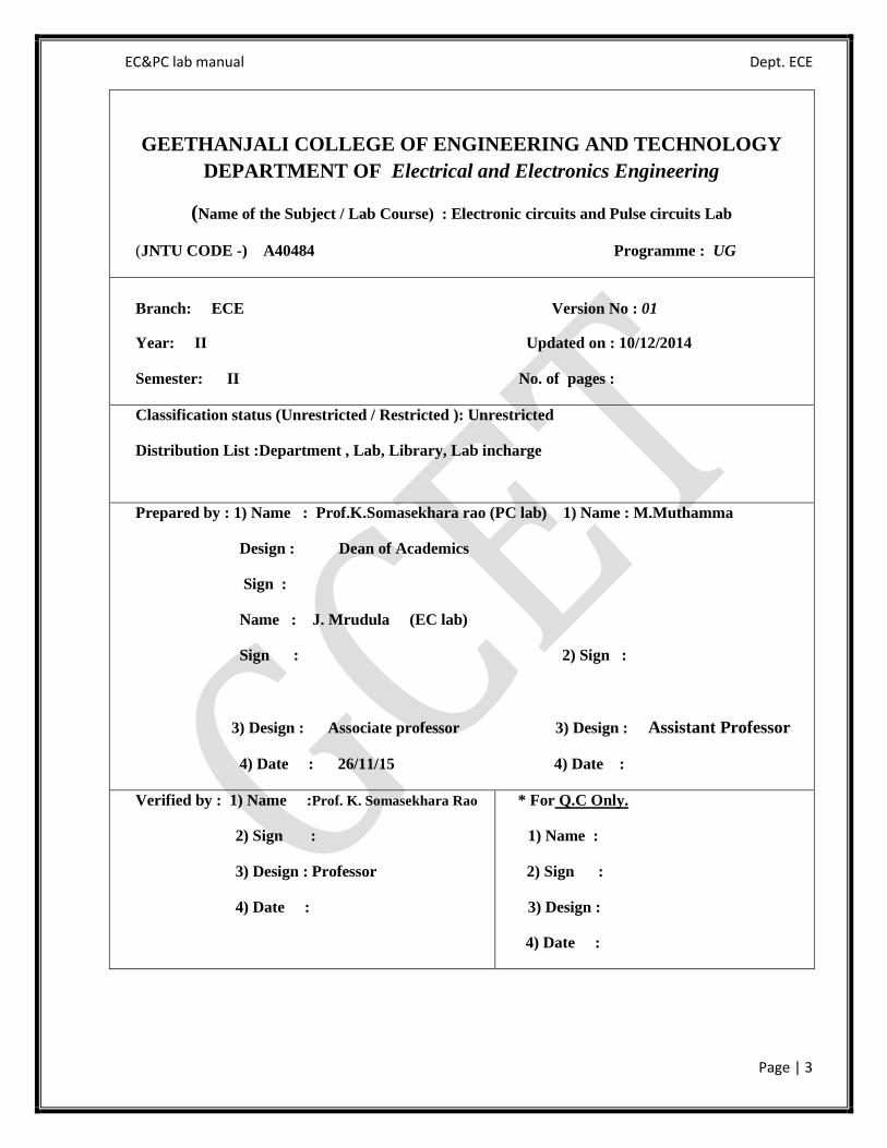
GEETHANJALI COLLEGE OF ENGINEERING AND TECHNOLOGY
DEPARTMENT OF Electrical and Electronics Engineering
(Name of the Subject / Lab Course) : Electronic circuits and Pulse circuits Lab
(JNTU CODE -) A40484 Programme : UG
Branch: ECE Version No : 01
Year: II Updated on : 10/12/2014
Semester: II No. of pages :
Classification status (Unrestricted / Restricted ): Unrestricted
Distribution List :Department , Lab, Library, Lab incharge
Prepared by : 1) Name : Prof.K.Somasekhara rao (PC lab) 1) Name : M.Muthamma
Design : Dean of Academics
Sign :
Name : J. Mrudula (EC lab)
Sign : 2) Sign :
3) Design : Associate professor 3) Design : Assistant Professor
4) Date : 26/11/15 4) Date :
Verified by : 1) Name :Prof. K. Somasekhara Rao
2) Sign :
3) Design : Professor
4) Date :
* For Q.C Only.
1) Name :
2) Sign :
3) Design :
4) Date :
EC&PC lab manual Dept. ECE
Page | 4
Approved by : (HOD ) 1) Name : Dr. P.Srihari
2) Sign :
3) Date :
EC&PC lab manual Dept. ECE
Page | 5
ECE DEPARTMENT
Vision of the Department
To impart quality technical education in Electronics and Communication Engineering
emphasizing analysis, design/synthesis and evaluation of hardware/embedded software using
various Electronic Design Automation (EDA) tools with accent on creativity, innovation and
research thereby producing competent engineers who can meet global challenges with societal
commitment.
Mission of the Department
i. To impart quality education in fundamentals of basic sciences, mathematics, electronics and
communication engineering through innovative teaching-learning processes.
ii. To facilitate Graduates define, design, and solve engineering problems in the field of
Electronics and Communication Engineering using various Electronic Design Automation
(EDA) tools.
iii. To encourage research culture among faculty and students thereby facilitating them to be
creative and innovative through constant interaction with R & D organizations and Industry.
iv. To inculcate teamwork, imbibe leadership qualities, professional ethics and social
responsibilities in students and faculty.
Program Educational Objectives of B. Tech (ECE) Program:
I. To prepare students with excellent comprehension of basic sciences, mathematics and
engineering subjects facilitating them to gain employment or pursue postgraduate studies
with an appreciation for lifelong learning.
II. To train students with problem solving capabilities such as analysis and design with
adequate practical skills wherein they demonstrate creativity and innovation that would
enable them to develop state of the art equipment and technologies of multidisciplinary
nature for societal development.
III. To inculcate positive attitude, professional ethics, effective communication and
interpersonal skills which would facilitate them to succeed in the chosen profession
exhibiting creativity and innovation through research and development both as team
member and as well as leader.
EC&PC lab manual Dept. ECE
Page | 6
Program Outcomes of B.Tech ECE Program:
1. An ability to apply knowledge of Mathematics, Science, and Engineering to solve complex
engineering problems of Electronics and Communication Engineering systems.
2. An ability to model, simulate and design Electronics and Communication Engineering
systems, conduct experiments, as well as analyze and interpret data and prepare a report
with conclusions.
3. An ability to design an Electronics and Communication Engineering system, component,
or process to meet desired needs within the realistic constraints such as economic,
environmental, social, political, ethical, health and safety, manufacturability and
sustainability.
4. An ability to function on multidisciplinary teams involving interpersonal skills.
5. An ability to identify, formulate and solve engineering problems of multidisciplinary
nature.
6. An understanding of professional and ethical responsibilities involved in the practice of
Electronics and Communication Engineering profession.
7. An ability to communicate effectively with a range of audience on complex engineering
problems of multidisciplinary nature both in oral and written form.
8. The broad education necessary to understand the impact of engineering solutions in a
global, economic, environmental and societal context.
9. A recognition of the need for, and an ability to engage in life-long learning and acquire the
capability for the same.
10. A knowledge of contemporary issues involved in the practice of Electronics and
Communication Engineering profession
11. An ability to use the techniques, skills and modern engineering tools necessary for
engineering practice.
12. An ability to use modern Electronic Design Automation (EDA) tools, software and
electronic equipment to analyze, synthesize and evaluate Electronics and Communication
Engineering systems for multidisciplinary tasks.
13. Apply engineering and project management principles to one's own work and also to
manage projects of multidisciplinary nature.
EC&PC lab manual Dept. ECE
Page | 7
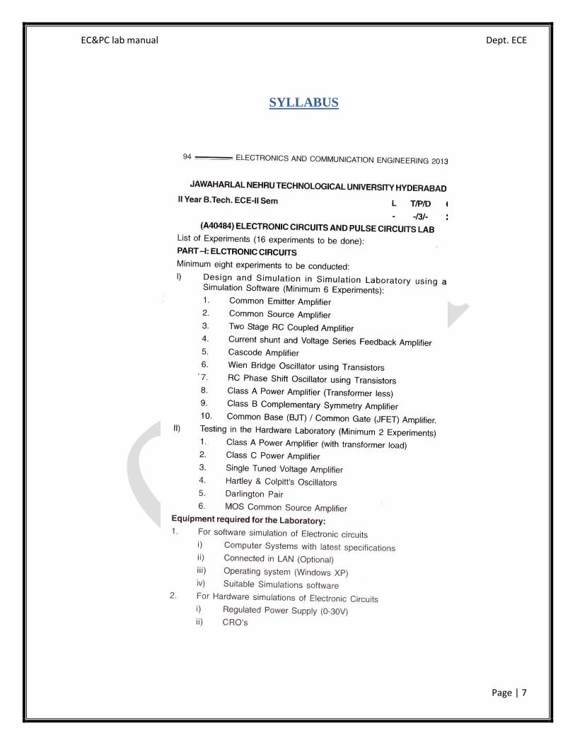
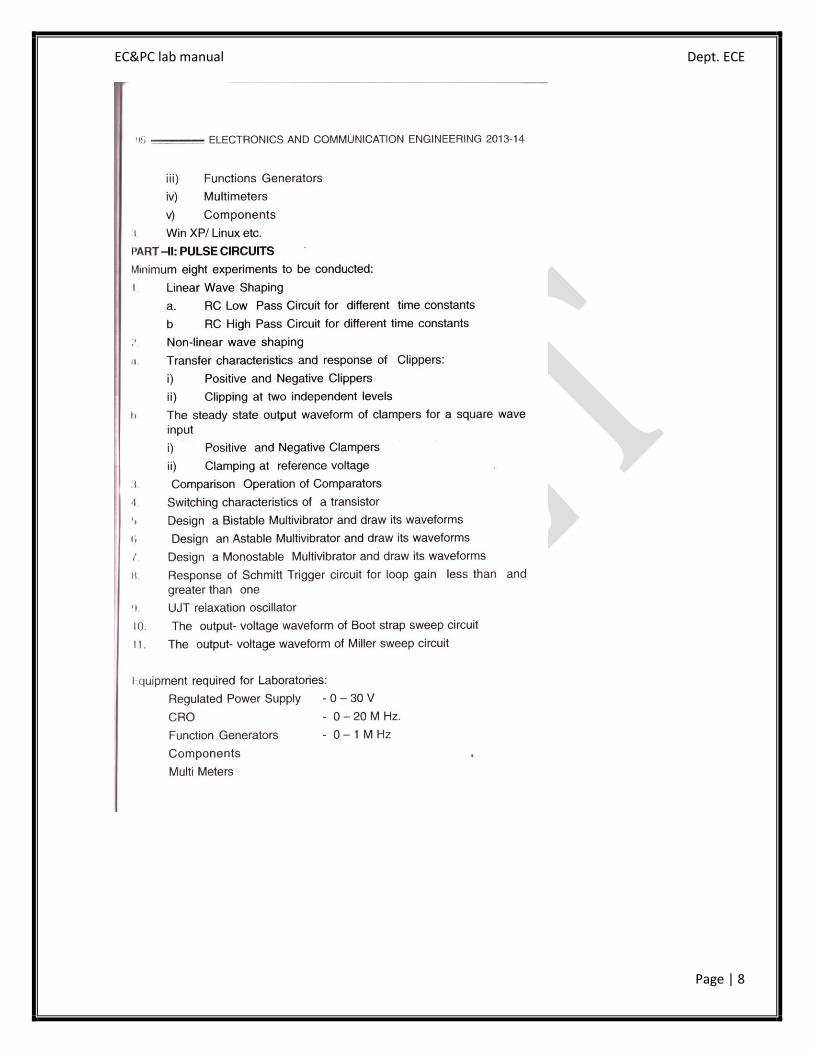
SYLLABUS
EC&PC lab manual Dept. ECE
Page | 8
EC&PC lab manual Dept. ECE
Page | 9
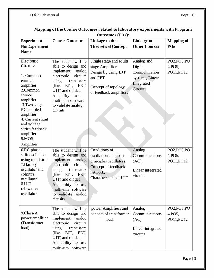
Mapping of the Course Outcomes related to laboratory experiments with Program
Outcomes (POs):
Experiment
No/Experiment
Name
Course Outcome Linkage to the
Theoretical Concept
Linkage to
Other Courses
Mapping of
POs
Electronic
Circuits:
1. Common
emitter
amplifier
2.Common
source
amplifier
3.Two stage
RC coupled
amplifier
4. Current shunt
and voltage
series feedback
amplifier
5.MOS
Amplifier
The student will be
able to design and
implement analog
electronic circuits
using transistors
(like BJT, FET,
UJT) and diodes.
An ability to use
multi-sim software
to validate analog
circuits
Single stage and Multi
stage Amplifier
Design by using BJT
and FET.
Concept of topology
of feedback amplifiers
Analog and
Digital
communication
systems, Linear
Integrated
Circuits
PO2,PO3,PO
4,PO5,
PO11,PO12
6.RC phase
shift oscillator
using transistors
7.Hartley
oscillator and
colpitt’s
oscillator
8.UJT
relaxation
oscillator
The student will be
able to design and
implement analog
electronic circuits
using transistors
(like BJT, FET,
UJT) and diodes.
An ability to use
multi-sim software
to validate analog
circuits
Conditions of
oscillations and basic
principles oscillators.
Concept of feedback
network,
Characteristics of UJT
Analog
Communications
(AC),
Linear integrated
circuits
PO2,PO3,PO
4,PO5,
PO11,PO12
9.Class-A
power amplifier
(Transformer
load)
The student will be
able to design and
implement analog
electronic circuits
using transistors
(like BJT, FET,
UJT) and diodes.
An ability to use
multi-sim software
power Amplifiers and
concept of transformer
load,
Analog
Communications
(AC),
Linear integrated
circuits
PO2,PO3,PO
4,PO5,
PO11,PO12
EC&PC lab manual Dept. ECE
Page | 10
to validate analog
circuits
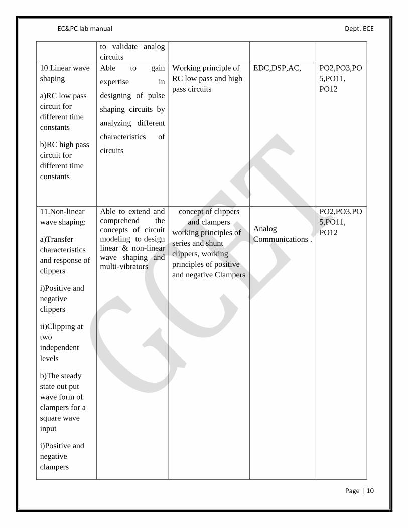
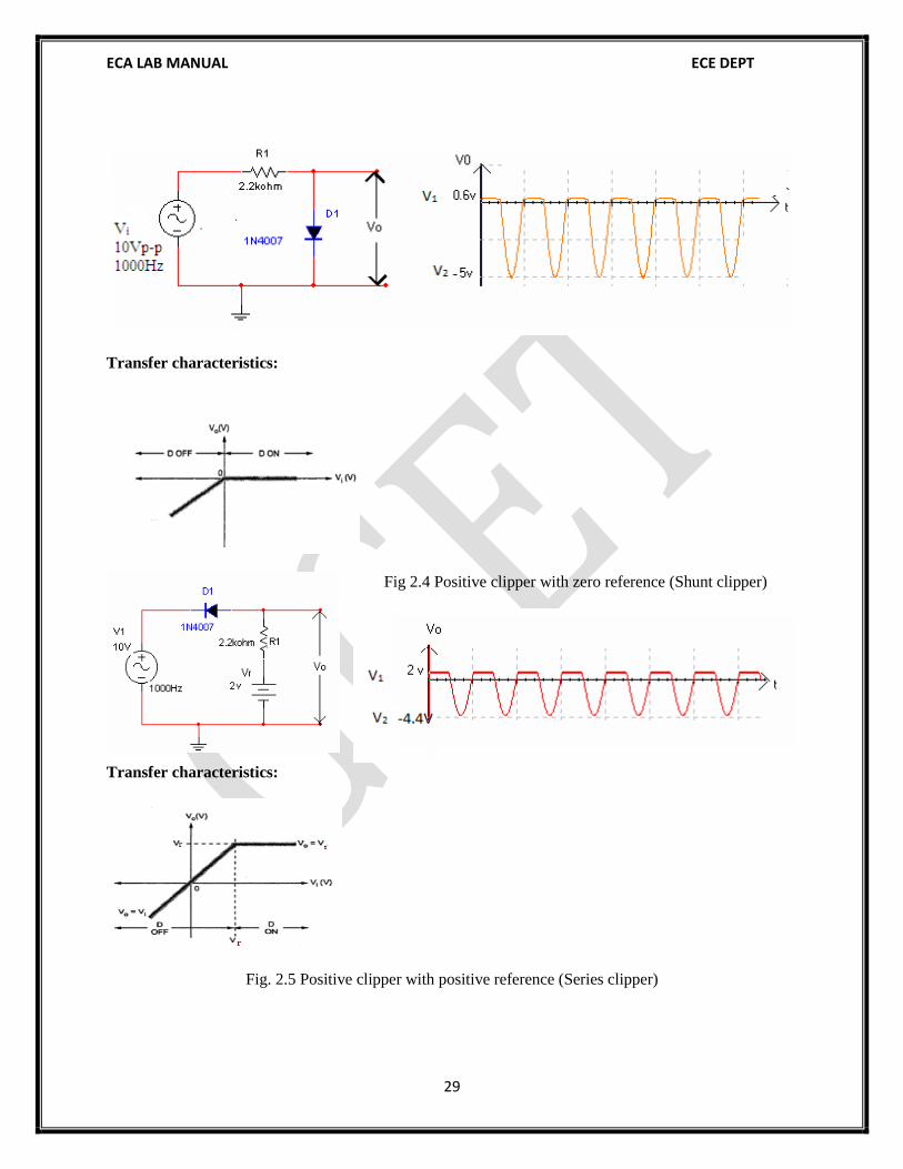
10.Linear wave
shaping
a)RC low pass
circuit for
different time
constants
b)RC high pass
circuit for
different time
constants
Able to gain
expertise in
designing of pulse
shaping circuits by
analyzing different
characteristics of
circuits
Working principle of
RC low pass and high
pass circuits
EDC,DSP,AC, PO2,PO3,PO
5,PO11,
PO12
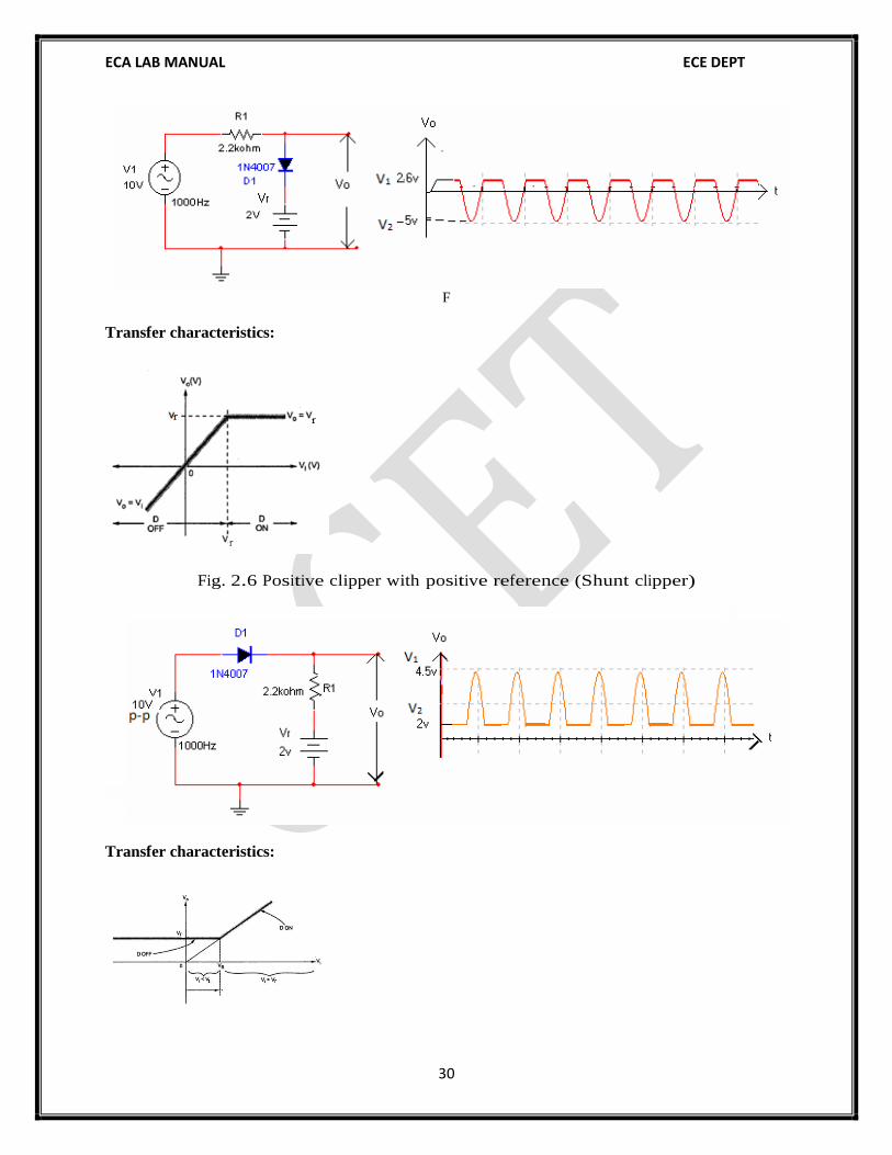
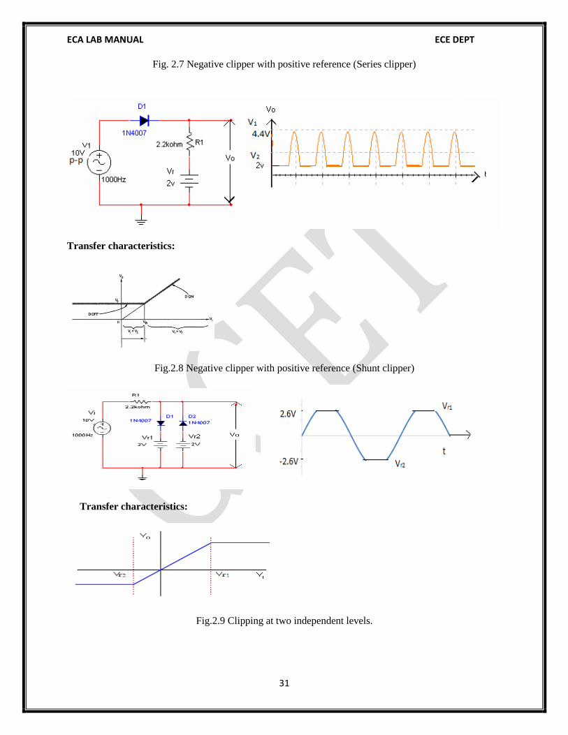
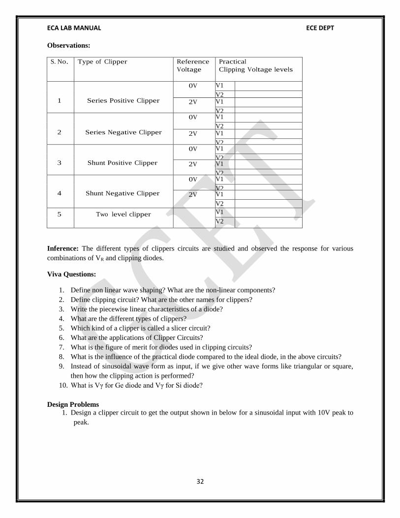
11.Non-linear
wave shaping:
a)Transfer
characteristics
and response of
clippers
i)Positive and
negative
clippers
ii)Clipping at
two
independent
levels
b)The steady
state out put
wave form of
clampers for a
square wave
input
i)Positive and
negative
clampers
Able to extend and
comprehend the
concepts of circuit
modeling to design
linear & non-linear
wave shaping and
multi-vibrators
concept of clippers
and clampers
working principles of
series and shunt
clippers, working
principles of positive
and negative Clampers
Analog
Communications .
PO2,PO3,PO
5,PO11,
PO12
EC&PC lab manual Dept. ECE
Page | 11
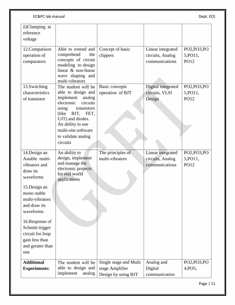
ii)Clamping at
reference
voltage
12.Comparison
operation of
comparators
Able to extend and
comprehend the
concepts of circuit
modeling to design
linear & non-linear
wave shaping and
multi-vibrators
Concept of basic
clippers
Linear integrated
circuits, Analog
communications
PO2,PO3,PO
5,PO11,
PO12
13.Switching
characteristics
of transistor
The student will be
able to design and
implement analog
electronic circuits
using transistors
(like BJT, FET,
UJT) and diodes.
An ability to use
multi-sim software
to validate analog
circuits
Basic concepts
operation of BJT
Digital integrated
circuits, VLSI
Design
PO2,PO3,PO
5,PO11,
PO12
14.Design an
Astable multi-
vibrators and
draw its
waveforms
15.Design an
mono stable
multi-vibrators
and draw its
waveforms
16.Response of
Schmitt trigger
circuit for loop
gain less than
and greater than
one
An ability to
design, implement
and manage the
electronic projects
for real world
applications
The principles of
multi-vibrators
Linear integrated
circuits, Analog
communications
PO2,PO3,PO
5,PO11,
PO12
Additional
Experiments:
The student will be
able to design and
implement analog
Single stage and Multi
stage Amplifier
Design by using BJT
Analog and
Digital
communication
PO2,PO3,PO
4,PO5,
EC&PC lab manual Dept. ECE
Page | 12
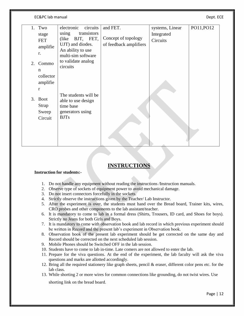
1. Two
stage
FET
amplifie
r.
2. Commo
n
collector
amplifie
r
3. Boot
Strap
Sweep
Circuit
electronic circuits
using transistors
(like BJT, FET,
UJT) and diodes.
An ability to use
multi-sim software
to validate analog
circuits
The students will be
able to use design
time base
generators using
BJTs
and FET.
Concept of topology
of feedback amplifiers
systems, Linear
Integrated
Circuits
PO11,PO12
INSTRUCTIONS
Instruction for students:-
1. Do not handle any equipment without reading the instructions /Instruction manuals.
2. Observe type of sockets of equipment power to avoid mechanical damage.
3. Do not insert connectors forcefully in the sockets.
4. Strictly observe the instructions given by the Teacher/ Lab Instructor.
5. After the experiment is over, the students must hand over the Bread board, Trainer kits, wires,
CRO probes and other components to the lab assistant/teacher.
6. It is mandatory to come to lab in a formal dress (Shirts, Trousers, ID card, and Shoes for boys).
Strictly no Jeans for both Girls and Boys.
7. It is mandatory to come with observation book and lab record in which previous experiment should
be written in Record and the present lab’s experiment in Observation book.
8. Observation book of the present lab experiment should be get corrected on the same day and
Record should be corrected on the next scheduled lab session.
9. Mobile Phones should be Switched OFF in the lab session.
10. Students have to come to lab in-time. Late comers are not allowed to enter the lab.
11. Prepare for the viva questions. At the end of the experiment, the lab faculty will ask the viva
questions and marks are allotted accordingly.
12. Bring all the required stationery like graph sheets, pencil & eraser, different color pens etc. for the
lab class.
13. While shorting 2 or more wires for common connections like grounding, do not twist wires. Use
shorting link on the bread board.
EC&PC lab manual Dept. ECE
Page | 13
Instructions to Laboratory Teachers:-
1. Observation book and lab records submitted for the lab work are to be checked and signed before
the next lab session.
2. Students should be instructed to switch ON the power supply after the connections are checked by
the lab assistant / teacher.
3. The promptness of submission of records/ observation books should be strictly insisted by awarding
the marks accordingly.
4. Ask viva questions at the end of the experiment.
5. Do not allow students who come late to the lab class.
6. Encourage the students to do the experiments innovatively.
EC&PC lab manual Dept. ECE
Page | 14
PART- II PULSE CIRCUITS
INDEX.
SNO EXP.NAME PAGE NO
1. LINEAR WAVE SHAPING
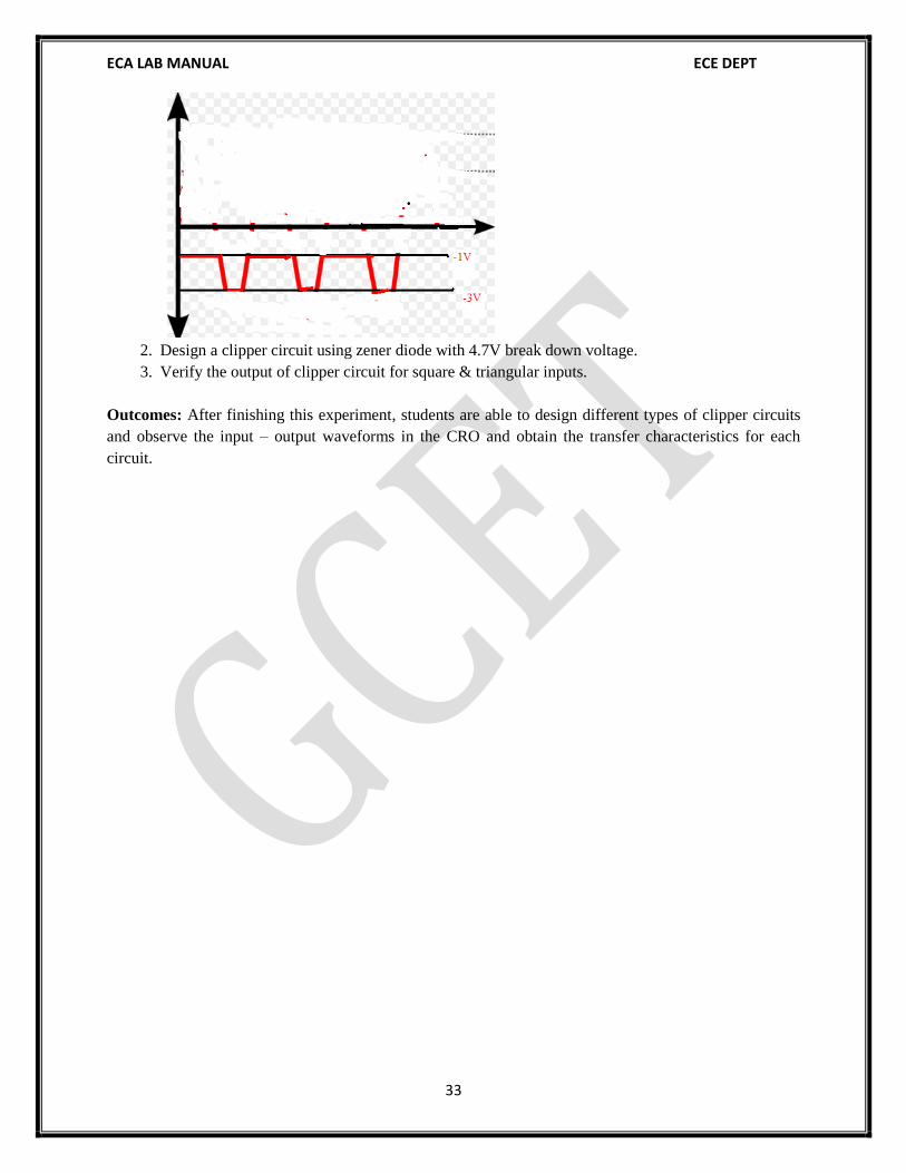
2. NON LINEAR WAVE SHAPING -CLIPPERS.
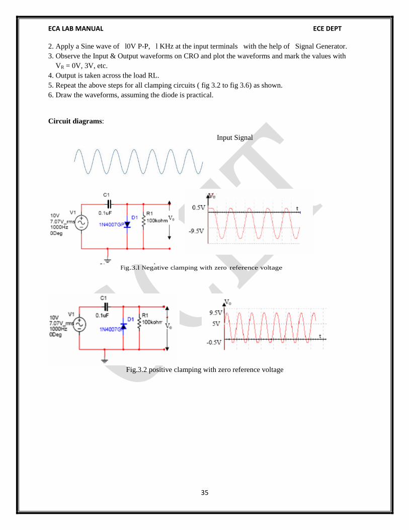
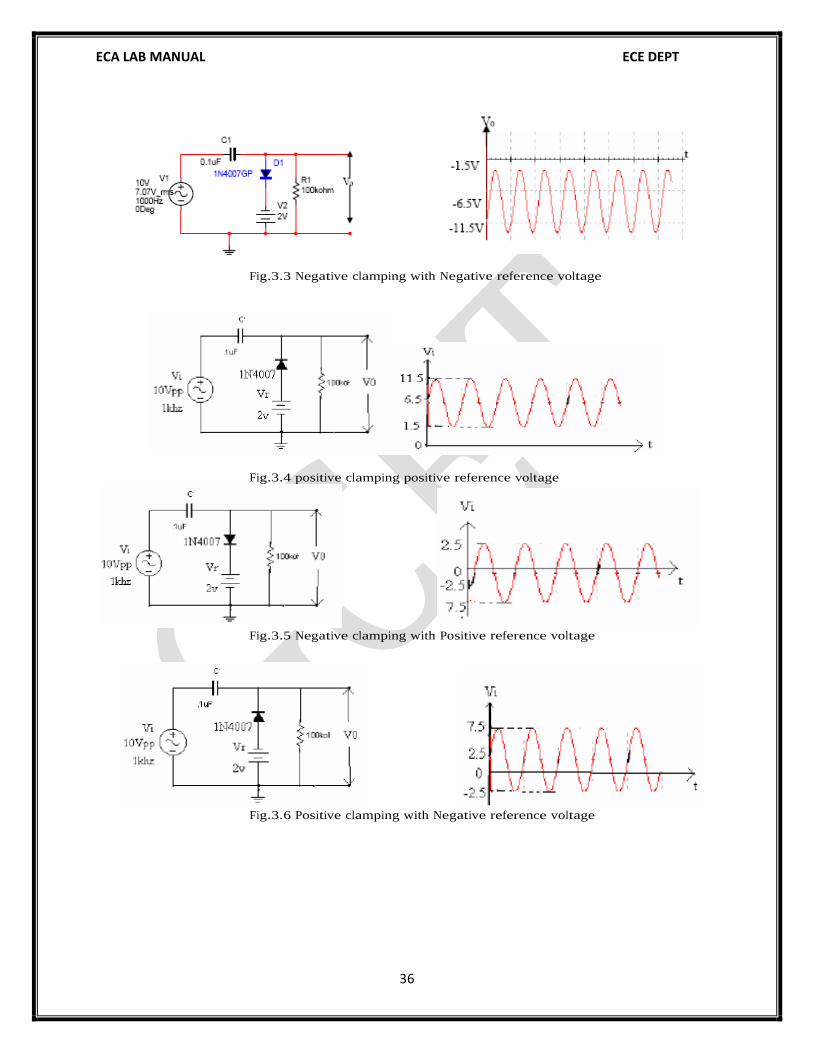
3. NON LINEAR WAVE SHAPING- CLAMPERS
4. SWITCHING CHARACTERISTICS OF TRANSISTOR
5. ASTABLE MULTIVIBRATOR
6. MONOSTABLE MULTIVIBRATOR
7. BISTABLE MULTIVIBRATOR.
8. UJT RELAXATION OSCILLATOR
ADDITIONAL EXPERIMENT
1 SCHMITT TRIGGER
2 BOOT STRAP SWEEP CIRCUIT
DESIGN EXPERIMENT
GENERATION OF DIFFERENT TYPES OF
WAVEFORMS FROM BASIC SINUSOIDAL
WAVEFORM
EC&PC lab manual Dept. ECE
Page | 15
PART-II
PULSE CIRCUITS
EC&PC lab manual Dept. ECE
Page | 16
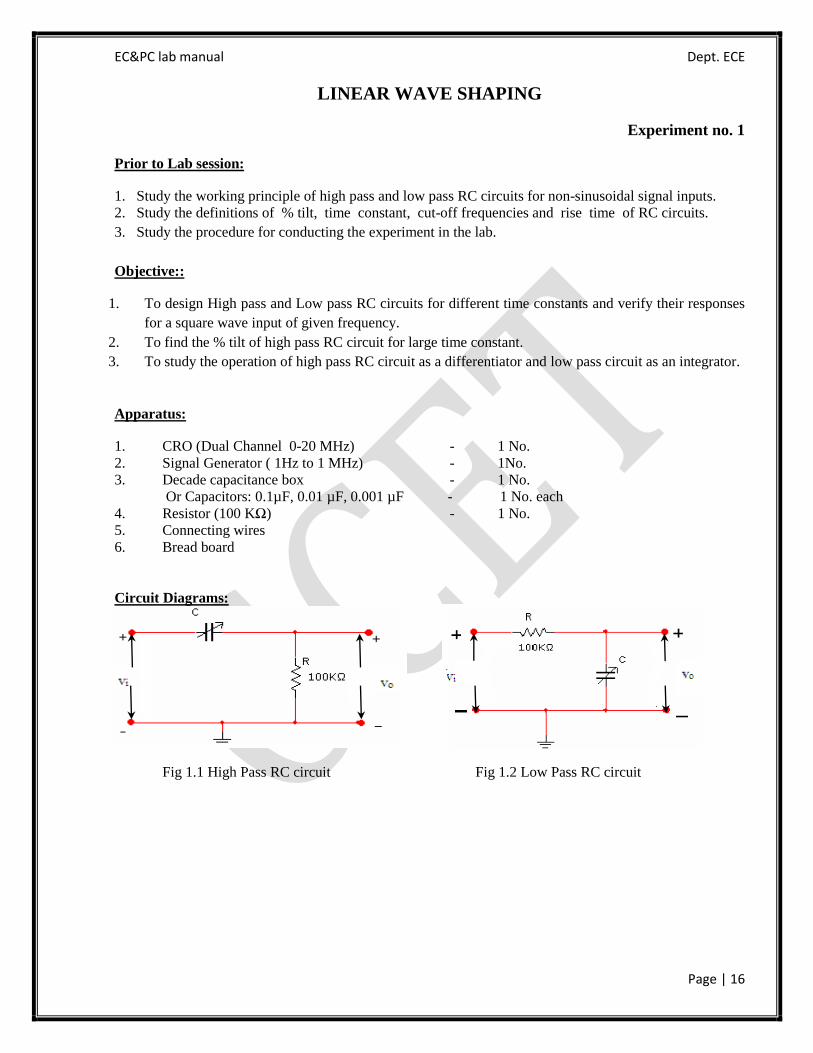
LINEAR WAVE SHAPING
Experiment no. 1
Prior to Lab session:
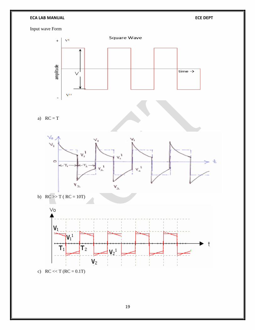
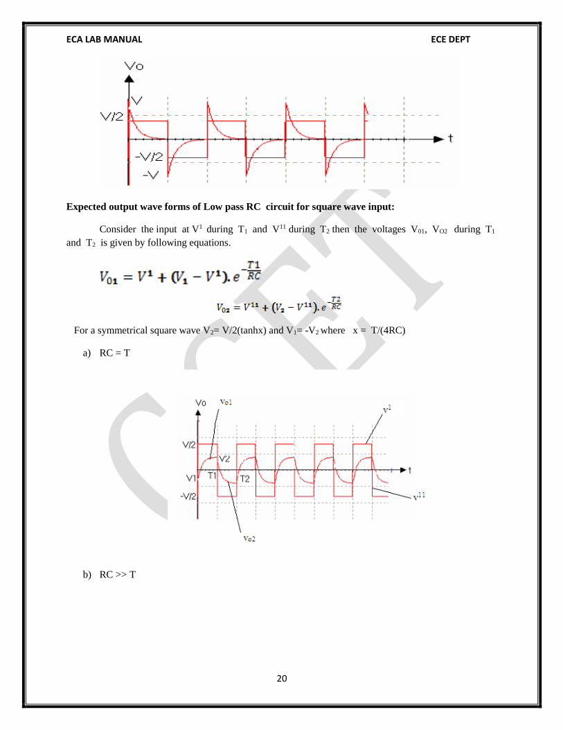
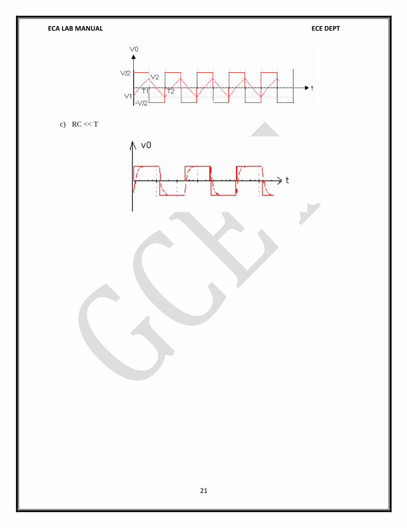
1. Study the working principle of high pass and low pass RC circuits for non-sinusoidal signal inputs.
2. Study the definitions of % tilt, time constant, cut-off frequencies and rise time of RC circuits.
3. Study the procedure for conducting the experiment in the lab.
Objective::
1. To design High pass and Low pass RC circuits for different time constants and verify their responses
for a square wave input of given frequency.
2. To find the % tilt of high pass RC circuit for large time constant.
3. To study the operation of high pass RC circuit as a differentiator and low pass circuit as an integrator.
Apparatus:
1. CRO (Dual Channel 0-20 MHz) - 1 No.
2. Signal Generator ( 1Hz to 1 MHz) - 1No.
3. Decade capacitance box - 1 No.
Or Capacitors: 0.1µF, 0.01 µF, 0.001 µF - 1 No. each
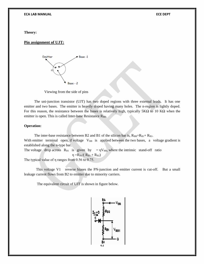
The uni-junction transistor (UJT) has two doped regions with three external leads. It has one
emitter and two bases. The emitter is heavily doped having many holes. The n-region is lightly doped.
For this reason, the resistance between the bases is relatively high, typically 5KΩ to 10 KΩ when the
emitter is open. This is called Inter-base Resistance RBB.
Operation:
The inter-base resistance between B2 and B1 of the silicon bar is, RBB=RB1+ RB2.
With emitter terminal open, if voltage VBB is applied between the two bases, a voltage gradient is
established along the n-type bar.
The voltage drop across RB1 is given by = ηVBB, where the intrinsic stand-off ratio
η =RB1/( RB1 + RB2)
The typical value of η ranges from 0.56 to 0.75.
This voltage V1 reverse biases the PN-junction and emitter current is cut-off. But a small
leakage current flows from B2 to emitter due to minority carriers.
The equivalent circuit of UJT is shown in figure below.
ECA LAB MANUAL ECE DEPT
44
Fig.5.2 UJT equivalent circuit.
If a negative voltage is applied to the emitter, PN-junction remains reverse biased and the emitter
current is cut-of. The device is now in the ‘OFF’ state.
If a positive voltage VE is applied to the emitter, the PN-junction will remain reverse biased so
long as VE is less than Vi. If VE exceeds Vi by the cut-in voltage vy, the diode becomes forward
biased. Under this condition, holes are injected into n-type bar. These holes are repelled by the terminal
B2 and are attracted by the terminal B1. Accumulations of holes in E to B1 region reduce the
resistance in this section and hence emitter current IE is increased and is limited by VE. The
device is now in the ‘ON’ state.
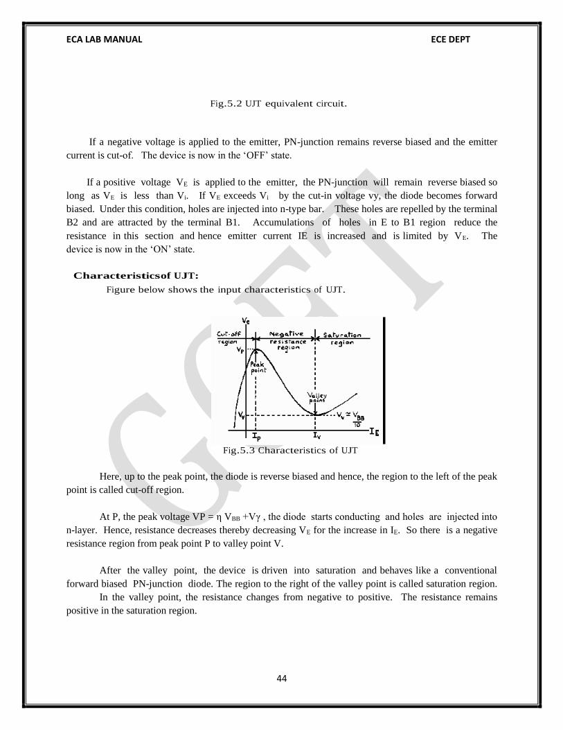
Characteristics of UJT:
Figure below shows the input characteristics of UJT.
Fig.5.3 Characteristics of UJT
Here, up to the peak point, the diode is reverse biased and hence, the region to the left of the peak
point is called cut-off region.
At P, the peak voltage VP = η VBB +Vγ , the diode starts conducting and holes are injected into
n-layer. Hence, resistance decreases thereby decreasing VE for the increase in IE. So there is a negative
resistance region from peak point P to valley point V.
After the valley point, the device is driven into saturation and behaves like a conventional
forward biased PN-junction diode. The region to the right of the valley point is called saturation region.
In the valley point, the resistance changes from negative to positive. The resistance remains
positive in the saturation region.
ECA LAB MANUAL ECE DEPT
45
Due to the negative resistance property, a UJT can be employed in a variety of applications, viz.,
a saw-tooth wave generator, pulse generator, switching, and timing and phase control circuits.
Frequency of oscillations:
The time period and hence the frequency of the saw-tooth wave can be calculated as follows:
Assuming that the capacitor is initially uncharged, the voltage VC across the capacitor prior to breakdown
is given by
VC = VBB (1- e –t/ RE
CE)
Where RECE = charging time constant of resistor-capacitor circuit, and t= time from the
commencement of the waveform.
The discharge of the capacitor occurs when VC is equal to the peak-point voltage VP, i.e,
VP = ηVBB = VBB (1- e –t/ RE
CE)
η = 1- e –t/ RE
CE
e –t/ RE
CE = 1- η
t = RECE loge(1/(1- η))
= 2.303 RECE log10(1/(1- η))
If the discharge time of the capacitor is neglected, then t=T, the period of the wave.
Therefore, frequency of oscillations of saw-tooth wave,
F = 1/T = 1/(2.303 RECE log10(1/(1- η)))
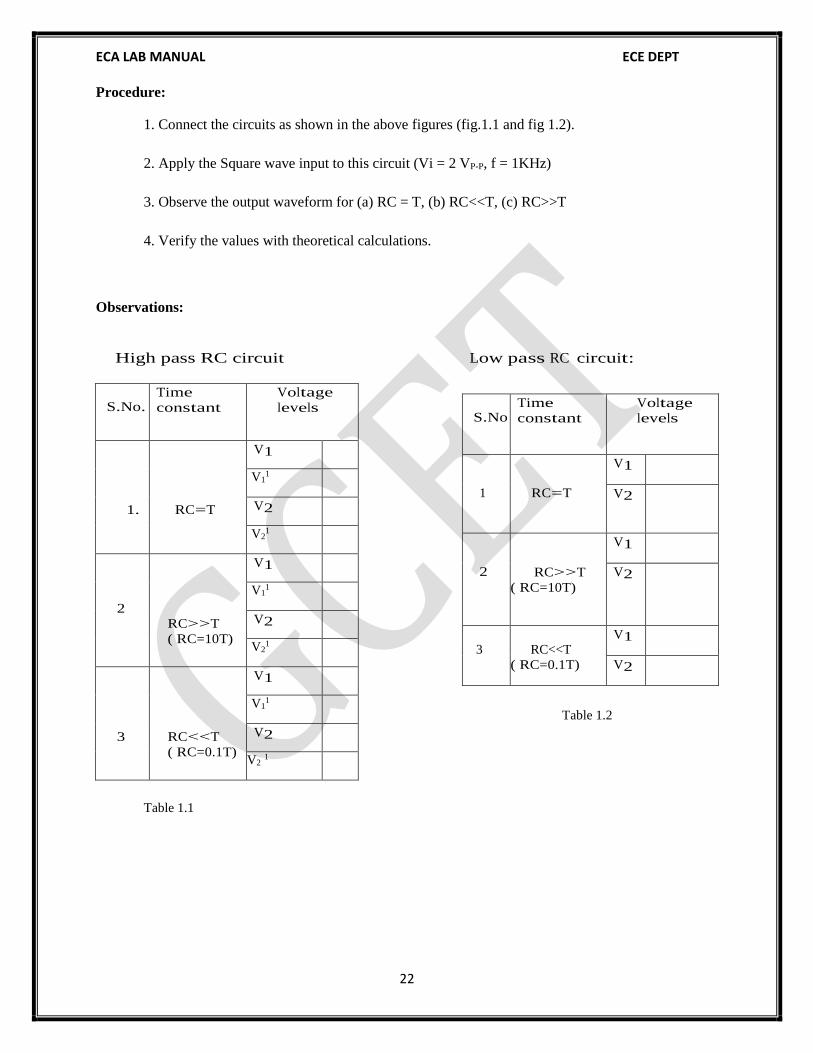
Procedure
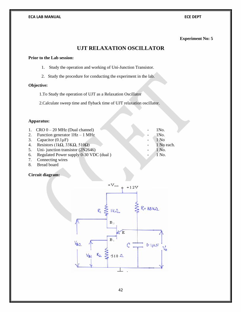
1. Connect the circuit as shown in figure.
2. Apply 12V DC power supply to the circuit.
3. Observe the output waveform on the CRO at B1, B2 and VO and Plot the graphs
4. Vary the time constant (RC) by varying capacitor (C) or potentiometer (R) and observe the variations
in the output pulses on the CRO at B1, B2 and VO.
ECA LAB MANUAL ECE DEPT
46
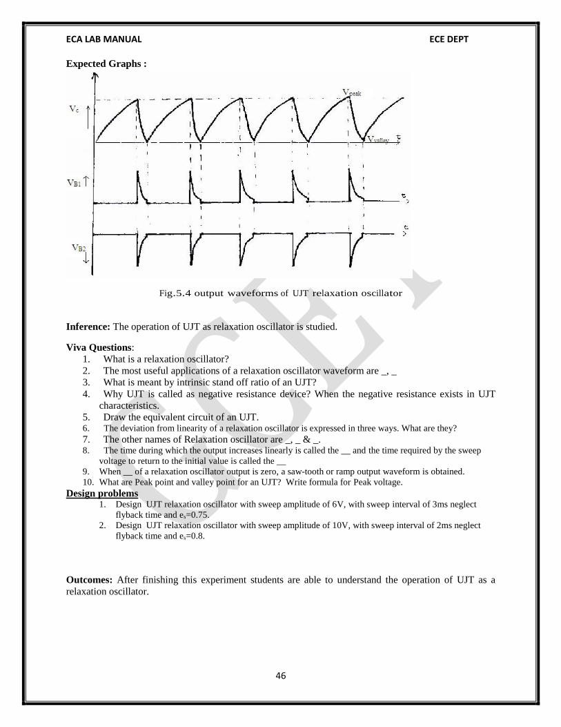
Expected Graphs :
Fig.5.4 output waveforms of UJT relaxation oscillator
Inference: The operation of UJT as relaxation oscillator is studied.
Viva Questions:
1. What is a relaxation oscillator?
2. The most useful applications of a relaxation oscillator waveform are _, _
3. What is meant by intrinsic stand off ratio of an UJT?
4. Why UJT is called as negative resistance device? When the negative resistance exists in UJT
characteristics.
5. Draw the equivalent circuit of an UJT. 6. The deviation from linearity of a relaxation oscillator is expressed in three ways. What are they?
7. The other names of Relaxation oscillator are _, _ & _. 8. The time during which the output increases linearly is called the __ and the time required by the sweep
voltage to return to the initial value is called the __
9. When __ of a relaxation oscillator output is zero, a saw-tooth or ramp output waveform is obtained.
10. What are Peak point and valley point for an UJT? Write formula for Peak voltage.
Design problems 1. Design UJT relaxation oscillator with sweep amplitude of 6V, with sweep interval of 3ms neglect
flyback time and es=0.75.
2. Design UJT relaxation oscillator with sweep amplitude of 10V, with sweep interval of 2ms neglect
flyback time and es=0.8.
Outcomes: After finishing this experiment students are able to understand the operation of UJT as a
relaxation oscillator.
ECA LAB MANUAL ECE DEPT
47
Experiment No. 6
ASTABLE MULTIVIBRATOR
Prior to the Lab session:
1. Study the operation and working principle of Astable Multivibrator.
2. Study the procedure for conducting the experiment in the lab.
Objective:
1. To study the operation and observe the wave forms of Astable Multivibrator.
2. To Design an Astable Multivibrator to generate a square wave of 1 KHz frequency using Transistor.
Apparatus:
1. CRO 0 to 20 MHz (Dual Channel) - 1 No.
2. Function Generator 1Hz to 1 MHz - 1 No.
3. Bread board - 1 No.
5. Resistor (1 KΩ, 10 KΩ) - 2 Nos each
6. Capacitors (0.1µF) - 2 Nos
6. Transistor (BC 107) - 2 Nos
7. Regulated D.C Power Supply 0 to 30V (dual) - 1 No.
8. Connecting wires
9. Bread board
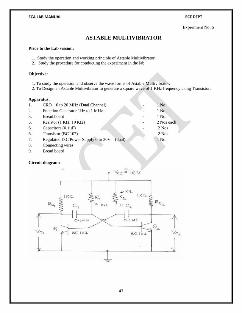
Circuit diagram:
ECA LAB MANUAL ECE DEPT
48
Theory:
The Astable circuit has two quasi-stable states. Without external triggering signal the Astable
configuration will make successive transitions from one quasi-stable state to the other. The Astable
circuit is an oscillator. It is also called as free running multivibrator and is used to generate “Square
Wave”. Since it does not require triggering signal, fast switching is possible.
Operation:
When the power is applied, due to some imbalance in the circuit, the transistor Q2
conducts more than Q1 i.e. current flowing through transistor Q2 is more than the current flowing in
transistor Q1. The voltage VC2 drops. This drop is coupled by the capacitor C1 to the base by Q1 there by
reducing its forward base-emitter voltage and causing Q1 to conduct less. As the current through Q1
decreases, VC1 rises. This rise is coupled by the capacitor C2 to the base of Q2. There by
increasing its base- emitter forward bias. This Q2 conducts more and more and Q1 conducts less and less,
each action reinforcing the other. Ultimately Q2 gets saturated and becomes fully ON and Q1 becomes
OFF. During this time C1 has been charging towards VCC exponentially with a time constant T1 = R1C1.
The polarity of C1 should be such that it should supply voltage to the base of Q1. When C1 gains sufficient
voltage, it drives Q1 ON. Then VC1 decreases and makes Q2 OFF. VC2 increases and makes Q1 fully
saturated. During this time C2 has been charging through VCC, R2, C2 and Qi with a time constant T2 =
R2C2. The polarity of C2 should be such that it should supply voltage to the base of Q2. When C2 gains
sufficient voltage, it drives Q2 ON, and the process repeats.
Design Procedure:
The period T is given by
T = T 1 + T2 = O.69 (R1C1 + R2C2)
For symmetrical circuit, with R1 = R2 = R & C1 = C2 = C
T = 1.38 RC
Let VCC = 12V; hfe = 51 (for BC107), VBESat = 0.7V; VCESat = 0.3V Let C = 0.1µF & T=1mSec.
T = 1.38 RC
10 -3 = 1.38 x R X 0.1 X 10⁻⁶
R = 7.24 KΩ (Practically choose 10KΩ) i.e R1 and R2 resistors.
Let ICmax=10mA
RC= = = 1.17KΩ ( 1 KΩ is selected for Rc1 and Rc2)
ECA LAB MANUAL ECE DEPT
49
Procedure:
1. Make then connections as per the circuit diagram.
2. Observe the Base Voltage and Collector Voltages of Q1 & Q2 on CRO in DC mode and measure the
frequency (f = 1/T).
3. Trace the waveforms at collector and base as each transistor with the help of dual trace CRO and plot
the waveforms.
4. Verify the practical output frequency with theoretical values f = 1/T, where T = 1.38 RC
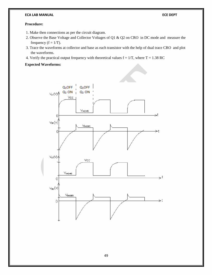
Expected Waveforms:
ECA LAB MANUAL ECE DEPT
50
Theoretical calculations: F= 1/ T= (1/1.38RC)
R= 10K Ω C=0.1µF
Result: An Astable Multivibrator is designed; the waveforms are observed and verified the results
theoretically.
Viva questions
1. What are the other names of Astable multivibrator?
2. The smaller allowable interval between two triggers is called the __ of the flip-flop. 3. Explain charging and discharging of capacitors in an Astable Multivibrator?
4. How can an Astable multivibrator be used as VCO?
5. What are symmetrical triggering and unsymmetrical triggering?
6. What are the applications of Astable Multivibrator?
7. Which multivibrator has two quasi-stable states? What is duty cycle?
8. What is the formula for frequency of oscillations? 9. An astable multivibrator is used as a ___ generator.
10. Design R and C for a frequency of 2KHz of a symmetric Astable oscillator.
Design problems
1. Design a collector coupled astable multivibrator using 2-BC107 transistors to operate at 1.5KHz
and with a duty cycle of 45% hfe min)=40, VCC=12V, IC(sat)=10mA.
2. Design voltage to frequency converter using astable multivibrator.
Outcomes: After finishing this experiment students are able to design Astable Multivibrator and explain
the operation of the same.
ECA LAB MANUAL ECE DEPT
51
Experiment No: 7
MONOSTABLE MULTIVIBRATOR
Pre-Lab:
1. Study the operation and working principle Monostable Multivibrator.
2. Study the procedure for conducting the experiment in the lab.
Objectives:
1. To study the operation and observe the wave forms of Monostable Multivibrator.
2. To Design a Monostable multivibrator for the pulse width of 0.3mSec.
Apparatus:
1. CRO 0 to 20 MHz (Dual channel) - 1No.
2. Function generator 1Hz to 1 MHz - 1No.
3. Capacitors (0.033µF) - 2 No.
4. Capacitor(0.01 µF)) - 1 No.
5. Resistors (1 kΩ, 10kΩ, 100KΩ, 47KΩ) - 2, 2, 1 and 1 Nos .
6. Transistor (BC 107) - 2 No.
7. Diode(IN4148) - 1 No.
8. Regulated Power supply 0 – 30 V(dual ) - 1 No.
9. Connecting wires
10. Bread board
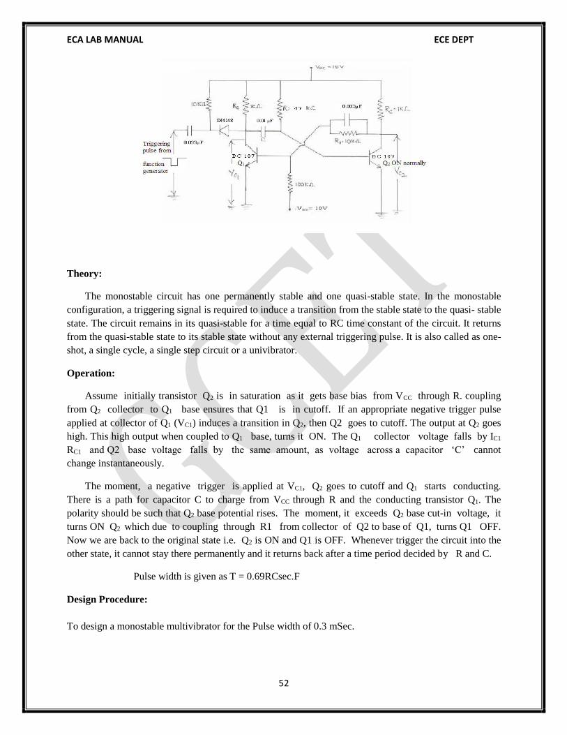
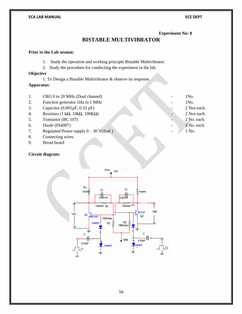
Circuit diagram:
ECA LAB MANUAL ECE DEPT
52
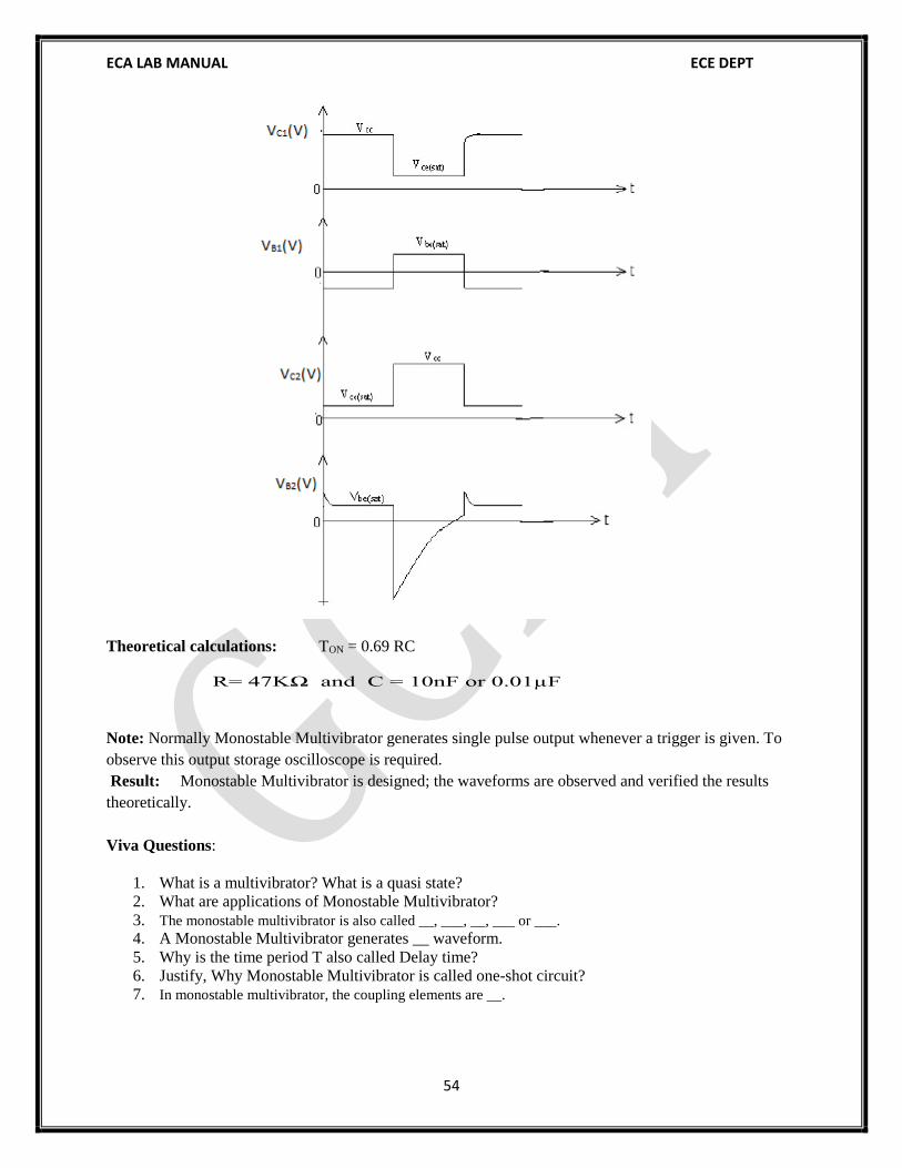
Theory:
The monostable circuit has one permanently stable and one quasi-stable state. In the monostable
configuration, a triggering signal is required to induce a transition from the stable state to the quasi- stable
state. The circuit remains in its quasi-stable for a time equal to RC time constant of the circuit. It returns
from the quasi-stable state to its stable state without any external triggering pulse. It is also called as one-
shot, a single cycle, a single step circuit or a univibrator.
Operation:
Assume initially transistor Q2 is in saturation as it gets base bias from VCC through R. coupling
from Q2 collector to Q1 base ensures that Q1 is in cutoff. If an appropriate negative trigger pulse
applied at collector of Q1 (VC1) induces a transition in Q2, then Q2 goes to cutoff. The output at Q2 goes
high. This high output when coupled to Q1 base, turns it ON. The Q1 collector voltage falls by IC1
RC1 and Q2 base voltage falls by the same amount, as voltage across a capacitor ‘C’ cannot
change instantaneously.
The moment, a negative trigger is applied at VC1, Q2 goes to cutoff and Q1 starts conducting.
There is a path for capacitor C to charge from VCC through R and the conducting transistor Q1. The
polarity should be such that Q2 base potential rises. The moment, it exceeds Q2 base cut-in voltage, it
turns ON Q2 which due to coupling through R1 from collector of Q2 to base of Q1, turns Q1 OFF.
Now we are back to the original state i.e. Q2 is ON and Q1 is OFF. Whenever trigger the circuit into the
other state, it cannot stay there permanently and it returns back after a time period decided by R and C.
Pulse width is given as T = 0.69RCsec.F
Design Procedure:
To design a monostable multivibrator for the Pulse width of 0.3 mSec.
A Bistable multivibratior is used in a many digital operations such as counting and the storing
of binary information. It is also used in the generation and processing of pulse-type
waveform. They can be used to control digital circuits and as frequency dividers.
There are two outputs available which are complements of one another. i.e. when one output is
high the other is low and vice versa .
Operation:
When VCC is applied, one transistor will start conducting slightly more than that of the other,
because of some differences in the characteristics of a transistor. Let Q2 be ON and Q1 be OFF. When Q2
is ON, The potential at the collector of Q2 decreases, which in turn will decrease the potential at the
base of Q1 due to potential divider action of R1 and R2. The potential at the collector of Q1
increases which in turn further increases the base to emitter voltage at the base of Q2. The voltage at the
collector of Q2 further decreases, which in turn further reduces the voltage at the base of Q1. This action
will continue till Q2 becomes fully saturated and Q1 becomes fully cutoff.
Thus the stable state of binary is such that one device remains in cut-off and other device
remains at saturation. It will be in that state until the triggering pulse is applied to it. It has two stable
states. For every transition of states triggering is required. At a time only one device will be conducting.
NEED OF COMMUTATING CAPACITORS (SPEED UP CAPACITORS):
It is desired that the transition should take place as soon as the trigger pulse is applied but such is
not the case.
When transistor is in active region it stores charge in its base and when it is in the
saturation region it stores even more charge. Hence transistor cannot come out of saturation to cut- off.
Until all such charges are removed. The interval during which conduction transfer one transistor to other
is called as the transition
Design Procedure:
RC = = = 1KΩ
VB1 = +
ECA LAB MANUAL ECE DEPT
58
-1.2 = (-15R1+0.2R2) /(R1+R2) ; given R1=10KΩ
R2= 100KΩ
Fmax= (R1+R2)/2C R1 R2 R 1=10KΩ , R2 = 100KΩ and C= 0.1µF
= (10+100)X103/(2X0.3X10-6X10X100X106) = 55KHz
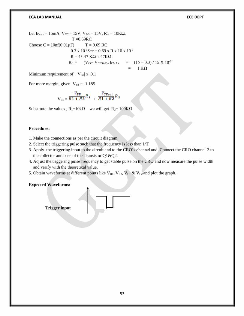
Procedure:
1. Make the connections as per the circuit diagram.
2. Apply trigger pulse of 1 KHz 5v (p-p) from function generator.
3. Obtain waveforms at different points such as VB1, VB2, VC1 & VC2.
4. Trace the waveform at collector and base of each transistor with the help of dual trace CRO. Note the
Time relation of waveforms.
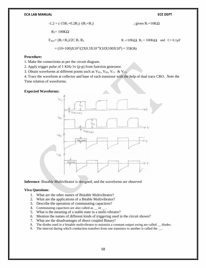
Expected Waveforms:
Inference: Bistable Multivibrator is designed; and the waveforms are observed
Viva Questions:
1. What are the other names of Bistable Multivibrator?
2. What are the applications of a Bitable Multivibrator?
3. Describe the operation of commutating capacitors?
4. Commutating capacitors are also called as __ or __ . 5. What is the meaning of a stable state in a multi-vibrator?
6. Mention the names of different kinds of triggering used in the circuit shown?
7. What are the disadvantages of direct coupled Binary? 8. The diodes used in a bistable multivibrator to maintain a constant output swing are called __ diodes.
9. The interval during which conduction transfers from one transistor to another is called the __.
ECA LAB MANUAL ECE DEPT
59
10. What are the coupling elements of a Bi-stable Multivibrator? Design Projects
1. Design a fixed bias binary employing two n-p-n silicon transistor to operate max frequency of
16KHz, VCC=VBB=10V, IC(sat)=5mA, hfe(min)=30.
2. Design and verify the bistable multivibrator by using different triggering methods.
Outcomes: After finishing this experiment students are able to design Bistable Multivibrator and able to
explain its operation.
ECA LAB MANUAL ECE DEPT
60
Experiment : 9
ADDITIONAL EXPERIMENT
SCHMITT TRIGGER
Pre-Lab:
1. Study the operation and working principle of Schmitt Trigger.
2. Study the procedure for conducting the experiment in the lab.
Objectives:
1. To design the circuit of Schmitt trigger with UTP=2.2V and LTP=1V.
2. To obtain square wave from sine wave.
3. To obtain UTP and LTP values practically
Apparatus:
1. CRO 0-20 MHz (Dual channel) - 1No.
2. Function generator 0- 1MHz - 1No.
3. Capacitor (0.1µF) - 1 No.
4. Resistors (1kΩ, 2.2KΩ, 330Ω) - 1 No. each
5. Resistor (1.2 KΩ) - 3 No.
6. Transistor (BC 107) - 2 No.
7. Regulated Power supply 0-30 V (dual ) - 1 No.
8. Connecting wires
9. Bread board
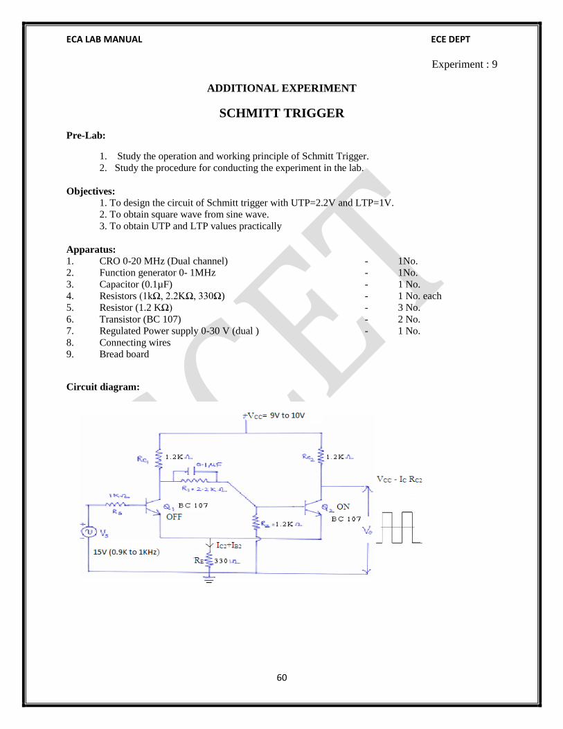
Circuit diagram:
ECA LAB MANUAL ECE DEPT
61
Theory:
In digital circuits fast waveforms are required i.e, the circuit remain in the active region for a
very short time (of the order of nano seconds) to eliminate the effects of noise or undesired parasitic
oscillations causing malfunctions of the circuit. Also if the rise time of the input waveform is long,
it requires a large coupling capacitor. Therefore circuits which can convert a slow changing
waveform (long rise time) in to a fast changing waveform (small rise time) are required. The
circuit which performs this operation is known as “Schmitt Trigger”.
In Schmitt trigger circuit, the output is in one of the two levels namely low or high. When
the input voltage is raising above the UTP (upper threshold point) i.e. V1, the output changes to high
level. Similarly when a falling output voltage passes through a voltage V2 known as lower
threshold point (LTP), the output changes to low. The level of the output changes V1 is always greater
than V2.The differences of these two voltages is known as “Hysteresis”.
Design Procedure:
The voltage required to drive the transistor Q1 from CFF to CN is called upper trigger point.
UTP = V1 = V1 — 0.1
Where V1 = V = ( VCCR2)/ (R1+R2+RC1)
The voltage required to drive the transistor Q1 from ON to OFF is called lower trigger point.
LTP = V2= VBE(active)+ (V1-Vγ2) .Re/(aRcth+Re)
Where Rcth =(RC1(R1+R2))/( R1+R2+RC1) a =R2/(R1+R2)
Choose BC107 transistor with hfe= 200
Let Vcc=12V, R1=2.2KΩ , R2=1.2KΩ
Set UTP = V1 — 0.1 2.2= V1 — 0.1 V1= 2.3V
But V1= (12X15)/(2.2+1.5+RC1) RC1=4.12KΩ= 4KΩ
Rcth = (4X 10³(2.2+1.5))/(2.1+1.2+4.4K) = 1.97KΩ
a= 0.3529
LTP =V2= VBE(active)+ (V1-Vγ2) .Re/(aRcth+Re)
= 0.7+(2.3-0.6).330/(0.35X1.97K+330)
= 1.21V
VE=V1-VBE= 2.3-0.7 = 1.6V
IB2= VE/RE(1+hfe) = 1.6/330(1+200) = 0.0030A
IC2 = hfeIB2 =0.6V
When Vin < V2, output =1V
ECA LAB MANUAL ECE DEPT
62
(VC-output)/IC2 = RC2 (12-1)/0.6 = RC2= 18.33Ω
Procedure:
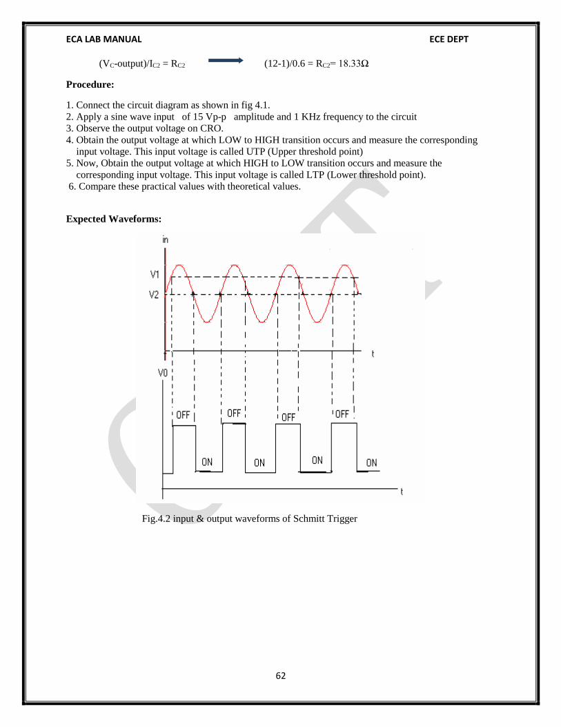
1. Connect the circuit diagram as shown in fig 4.1.
2. Apply a sine wave input of 15 Vp-p amplitude and 1 KHz frequency to the circuit
3. Observe the output voltage on CRO.
4. Obtain the output voltage at which LOW to HIGH transition occurs and measure the corresponding
input voltage. This input voltage is called UTP (Upper threshold point)
5. Now, Obtain the output voltage at which HIGH to LOW transition occurs and measure the
corresponding input voltage. This input voltage is called LTP (Lower threshold point).
6. Compare these practical values with theoretical values.
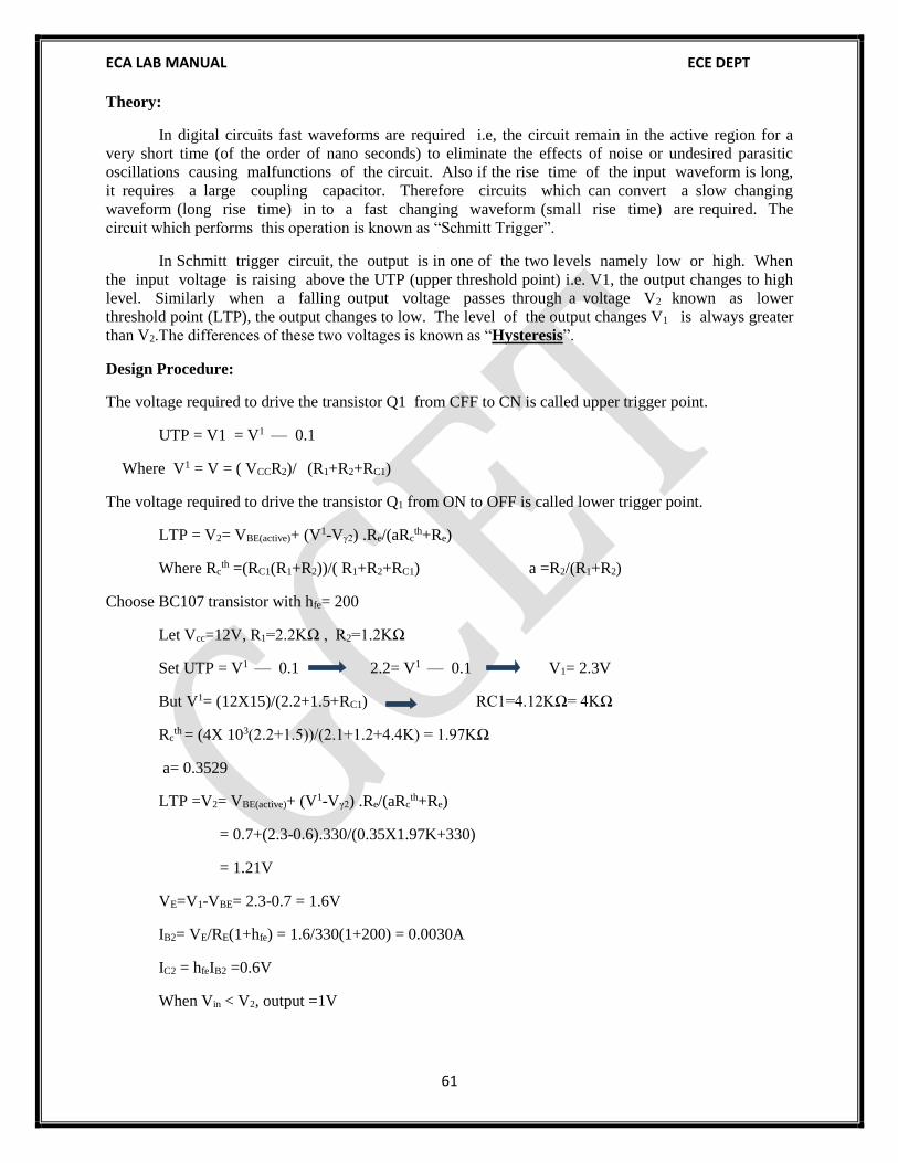
Expected Waveforms:
Fig.4.2 input & output waveforms of Schmitt Trigger
ECA LAB MANUAL ECE DEPT
63
Inference: Schmitt trigger circuit with the given values is designed; and the response is observed.
Viva Questions:
1. What is Schmitt Trigger?
2. What are the applications of Schmitt Trigger?
3. Define hysteresis action?
4. Why Schmitt Trigger is called a squaring circuit?
5. Define UTP? Write its expression.
6. Define LTP? Write its expression.
7. What is the difference between a Binary and Schmitt Trigger?
8. How noise can be eliminated on a given signal using Schmitt Trigger?
9. Explain how a Schmitt Trigger converts a sine wave to a square wave?
10. A Schmitt trigger exhibits hysteresis when loop gain is ___.
Design Projects
1. Design Schmitt trigger circuit to get UTP=5V and LTP=7V for VCC=15V.
Outcomes: After finishing this experiment students are able to Design Schmitt trigger circuit using
transistor and they are able to find UTP and LTP.
ECA LAB MANUAL ECE DEPT
64
Experiment 10
BOOT STRAP SWEEP CIRCUIT
Pre-Lab:
1. Study the operation and working principle of Boot-strap Sweep Circuit.
2. Study the procedure for conducting the experiment in the lab.
Objectives:
1. To design a Boot-strap Sweep Circuit.
2. To obtain a sweep wave form.
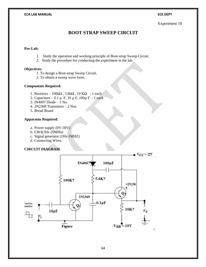
Components Required:
1. Resistors – 100kΩ , 5.6kΩ , 10 KΩ - 1 each
2. Capacitors – 0.1 µ F, 10 µ F, 100µ F - 1 each
3. IN4007 Diode – 1 No.
4. 2N2369 Transistors – 2 Nos.
5. Bread Board
Apparatus Required:
a. Power supply (0V-30V)
b. CRO(1Hz-20MHz)
c. Signal generator (1Hz-1MHZ)
d. Connecting Wires.
CIRCUIT DIAGRAM
ECA LAB MANUAL ECE DEPT
65
THEORY:
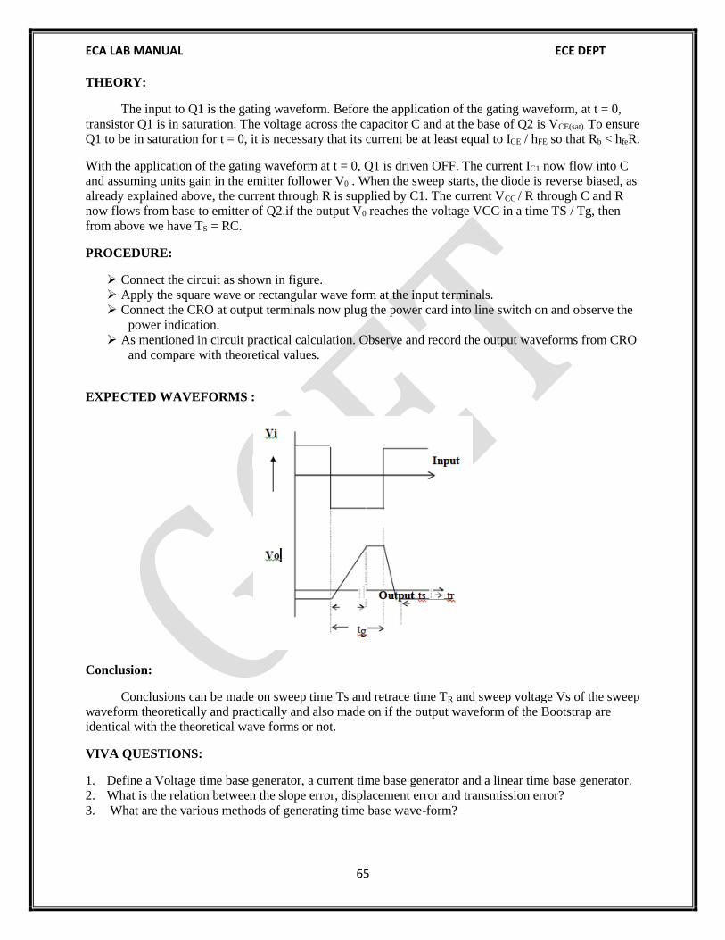
The input to Q1 is the gating waveform. Before the application of the gating waveform, at t = 0,
transistor Q1 is in saturation. The voltage across the capacitor C and at the base of Q2 is VCE(sat). To ensure
Q1 to be in saturation for t = 0, it is necessary that its current be at least equal to ICE / hFE so that Rb < hfeR.
With the application of the gating waveform at t = 0, Q1 is driven OFF. The current IC1 now flow into C
and assuming units gain in the emitter follower V0 . When the sweep starts, the diode is reverse biased, as
already explained above, the current through R is supplied by C1. The current VCC / R through C and R
now flows from base to emitter of Q2.if the output V0 reaches the voltage VCC in a time TS / Tg, then
from above we have TS = RC.
PROCEDURE:
Connect the circuit as shown in figure.
Apply the square wave or rectangular wave form at the input terminals.
Connect the CRO at output terminals now plug the power card into line switch on and observe the
power indication.
As mentioned in circuit practical calculation. Observe and record the output waveforms from CRO
and compare with theoretical values.
EXPECTED WAVEFORMS :
Conclusion:
Conclusions can be made on sweep time Ts and retrace time TR and sweep voltage Vs of the sweep
waveform theoretically and practically and also made on if the output waveform of the Bootstrap are
identical with the theoretical wave forms or not.
VIVA QUESTIONS:
1. Define a Voltage time base generator, a current time base generator and a linear time base generator.
2. What is the relation between the slope error, displacement error and transmission error?
3. What are the various methods of generating time base wave-form?
ECA LAB MANUAL ECE DEPT
66
4. Which amplifier is used in Boot-strap time base generator?
5. Which type of sweep does a bootstrap time-base generator produce?
6. What is the gain of the amplifier used in Bootstrap time base generator?
7. What is retrace time? Write the formula for the same for Bootstrap time base generator.
8. What is the formula for sweep amplitude in Bootstrap time base generator?
9. To have less flatness time of sweep signal, then the gate signal time has to be __.
10. A Bootstrap sweep circuit employs __ type of feedback.
Design problem:
1. Design Boot-strap Sweep Circuit with sweep amplitude of 8V, with sweep interval of 1ms neglect
flyback time and es=0.25.
2. Design Boot-strap Sweep Circuit with sweep amplitude of 15V, with sweep interval of 2ms neglect
flyback time and es=0.1.
Outcomes: After finishing this experiment students are able to Design Boot-strap sweep circuit and able
to generate a sweep voltage waveform.
ECA LAB MANUAL ECE DEPT
67
Design Experiment
GENERATION OF DIFFERENT TYPES OF WAVEFORMS FROM BASIC SINUSOIDAL