19
For Academic Use Only This material exempt per Department of Commerce license exception TSU Lab6 – HW/SW System Debug Targeting MicroBlaze™ on the Spartan-3E™ Starter Kit
| Date post: | 08-Mar-2018 |
| Category: |
Documents |
| Upload: | phungnguyet |
| View: | 222 times |
| Download: | 2 times |

For Academic Use Only
This material exempt per Department of Commerce license exception TSU
Lab6 – HW/SW System Debug
Targeting MicroBlaze™ on the Spartan-3E™ Starter Kit

HW/SW System Debug Lab: www.xilinx.com/university 6-1 MicroBlaze Processor [email protected]
Lab 6: HW/SW System Debug Lab
Introduction
This lab guides you through the process of performing on-chip hardware/software verification using
Chipscope-Pro and the software debugger.
Objectives
After completing this lab, you will be able to:
• Add ChipScope Analyzer cores into a system
• Cross debug with Chipscope Analayzer and the SDK debugger
Procedure You will extend the system created in the previous lab by adding Chipscope ICON and IBA cores. The
IBA core will be added to the PLB bus. You will set trigger conditions in the Chipscope Analyzer software
(running on PC) to capture bus transactions when the value of the count variable is written to the LEDs.
When the hardware trigger condition is met, you will see that the software debugger stops at the line of
code that was last executed. This lab comprises the following steps:
1. Open the lab 6 project
2. Instantiate Chipscope cores
3. Setup SDK and Chipscope
4. Perform hardware/software verification

HW/SW System Debug Lab: www.xilinx.com/university 6-2 MicroBlaze Processor [email protected]
Figure 6-1. Complete MicroBlaze System
For each procedure within a primary step, there are general instructions (indicated by the
symbol). These general instructions only provide a broad outline for performing the procedure. Below these general instructions, you will find accompanying step-by-step directions and
illustrated figures that provide more detail for performing the procedure. If you feel confident
about completing a procedure, you can skip the step-by-step directions and move on to the next
general instruction.
LMB
BRAM
CNTLR
LMB
BRAM
CNTLR
BRAM
PLB
MDM UART
INTC
MicroBlaze
Timer
GPIO
GPIO
IBAICON
PSB
LEDs
LCD MYIP
GPIODIP
BRAM
XPS
BRAM
CNTLR
MPMC
CNTLRDDR
LMB
BRAM
CNTLR
LMB
BRAM
CNTLR
LMB
BRAM
CNTLR
LMB
BRAM
CNTLR
BRAMBRAM
PLBPLB
MDMMDM UARTUART
INTCINTC
MicroBlazeMicroBlaze
TimerTimer
GPIOGPIO
GPIOGPIO
IBAIBAICONICON
PSB
LEDs
LCD MYIP
GPIOGPIODIP
BRAMBRAM
XPS
BRAM
CNTLR
MPMC
CNTLRDDR

HW/SW System Debug Lab: www.xilinx.com/university 6-3 MicroBlaze Processor [email protected]
Opening the Project Step 1
Create a lab6 folder under c:\xup\embedded\labs. If you wish to continue with
your completed design from lab5 then copy the contents of the lab5 folder into
the lab6 folder or copy the content of labsolution\lab5 folder into the lab6.
Launch Xilinx Platform Studio (XPS) and open the project file located in
c:\xup\embedded\ labs\lab6.
� Create a lab6 folder in the c:\xup\embedded\labs directory. If you wish to continue with your
completed design from lab5 then copy the contents of the lab5 folder into the lab6 folder, otherwise copy the content of labsolution\lab5 folder into the lab6 folder.
� Open XPS by clicking Start →→→→ All Programs →→→→ Xilinx ISE Design Suite 12 →→→→ EDK →→→→
Xilinx Platform Studio
� Select Open a recent project, Click OK and browse to C:\xup\embedded\labs\lab6
� Click system.xmp to open the project
Instantiate ChipScope Cores Step 2
Add the ChipScope cores using the Debug Configuration wizard. Configure the
device and the design to the following ports, as shown in the Figure 6-2. Setup
the trigger to trigger when a certain values are on the PLB address, PLB data, and
PLB control bus.
Figure 6-2. ChipScope Core Connections
� Select Debug ���� Debug Configuration

HW/SW System Debug Lab: www.xilinx.com/university 6-4 MicroBlaze Processor [email protected]
Figure 6-3. Debug Configuration Dialogue � Click the Add Chipscope Peripheral... button and select the first option, To monitor PLB
v4.6 bus signals (adding PLB IBA). Click OK.
Figure 6-4. Add the PLB IBA

HW/SW System Debug Lab: www.xilinx.com/university 6-5 MicroBlaze Processor [email protected]
� Click to put a check mark in the Bus Write Data Signals field and set the Select the Number
of signal samples you want to collect option to 512. Make sure you have the options
selected according to Figure 6-5.
Figure 6-5. Setting Basic Debug Configuration Options for the PLB_IBA
� Click the Advanced tab. Under the User tab, in the Trigger In, PLB Reset and PLB Error
Status panel, uncheck the Enable probing system reset and system error signals field and
set Match unit type to basic

HW/SW System Debug Lab: www.xilinx.com/university 6-6 MicroBlaze Processor [email protected]
Figure 6-6. Setting Trigger In, PLB Reset and PLB Error Status options
� Select Extended as the Match Unit Type for the PLB Address and PLB Write Data busses
Figure 6-7. Setting PLB Data options
� Click OK, and view the Bus Interface noting the newly added Chipscope Cores in the System
Assembly View

HW/SW System Debug Lab: www.xilinx.com/university 6-7 MicroBlaze Processor [email protected]
Figure 6-8. Chipscope Cores Automatically added to MicroBlaze System
� Select Hardware ���� Generate Bitstream
Setup SDK and ChipScope Step 3
Export the project to SDK project and establish a connection to the target using
XMD. Having successfully generated your design it is possible to begin viewing
it in operation using the SDK debugger and ChipScope Pro tools.
Starting the SDK debugger (Software Debug)
� Open SDK by selecting Project → Export Hardware Design to SDK …
� Check Include Bitstream and BMM File option and click on Export & Launch SDK
button.
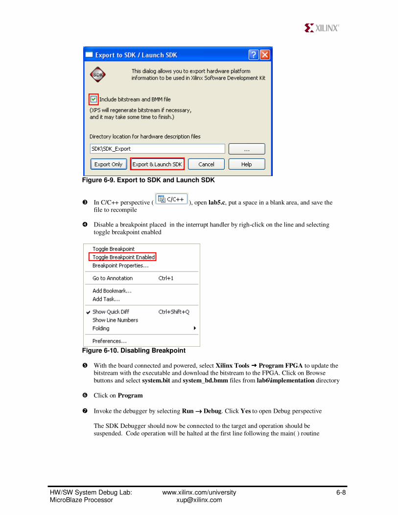
HW/SW System Debug Lab: www.xilinx.com/university 6-8 MicroBlaze Processor [email protected]
Figure 6-9. Export to SDK and Launch SDK
� In C/C++ perspective ( ), open lab5.c, put a space in a blank area, and save the file to recompile
� Disable a breakpoint placed in the interrupt handler by righ-click on the line and selecting
toggle breakpoint enabled
Figure 6-10. Disabling Breakpoint
� With the board connected and powered, select Xilinx Tools ���� Program FPGA to update the bitstream with the executable and download the bitstream to the FPGA. Click on Browse
buttons and select system.bit and system_bd.bmm files from lab6\implementation directory
� Click on Program
� Invoke the debugger by selecting Run →→→→ Debug. Click Yes to open Debug perspective
The SDK Debugger should now be connected to the target and operation should be
suspended. Code operation will be halted at the first line following the main( ) routine

HW/SW System Debug Lab: www.xilinx.com/university 6-9 MicroBlaze Processor [email protected]
Figure 6-11. SDK Debugger Connected to Target via XMD
Starting ChipScope Pro (Hardware Debug)
� Launch the ChipScope Pro Analyzer tool from the program group or desktop icon
� Click on the Open Cable/Search JTAG chain icon. This will identify the devices on the
JTAG chain. Click OK to open ChipScope Pro Analyzer with default Trigger Setup and
Waveform signal windows
Figure 6-12. ChipScope JTAG Device Order
� Select File →→→→ Import. In the Signal Import dialogue click on the Select New File button.
� Browse to the implementation directory and the select the following chipscope definition and connection file (CDC) C:\xup\embedded\labs\lab6\implementation
\chipscope_plbv46_iba_0_wrapper\chipscope_plbv46_iba_0.cdc and click OK
The CDC file contains signals associated with the PLB core which should now be listed in the
Trigger Setup and Waveform signal windows

HW/SW System Debug Lab: www.xilinx.com/university 6-10 MicroBlaze Processor [email protected]
� In the Waveform window, select all signals except PLB_RNW, right-click, and select
Remove from Viewer
� Select PLB_wrDBus and PLB_ABus in the Signals window, rightclick, and select Add to
View →→→→ Waveform
Figure 6-13. Chipscope Waveform View Setup
Perform HW/SW Verification Step 4
Setup the trigger to capture 32 data samples when count values greater than 5 are
written to the LEDs.
� Set M0:TRG0 PLB_RNW bit == 0 by clicking the + sign under M0 and selecting the
PLB_RNW bit and changing its value to 0 under Value field
� Change the Radix of M1 and M2 from binary (Bin) to Hexadecimal (Hex) by clicking on the respective boxes and selecting Hex
� Set M1:TRIG1 == 8144_0000 (or base address of LEDs_8Bit peripheral) and M2:TRIG2 >
0000_0005_0000_0000 (since we use only 32-bit data bus) by selecting and adjusting the
value box
� Click the field under Trigger Condition Equation, which opens the Trigger Condition:
TriggerCondition0 dialog box. Select M0 and Select M1, and then click OK to close
The Trigger Condition Equation field should now display M0 && M1. Click OK
� Set the trigger window depth to 32 and position to 0
� Set the Storage Qualification (M0 && M1&&M2) so that you capture count values greater
than 5 when written to the LEDs_8Bit peripheral.
Your settings should be similar to Figure 6-14.

HW/SW System Debug Lab: www.xilinx.com/university 6-11 MicroBlaze Processor [email protected]
Figure 6-14. Chipscope Trigger Settings
� Setup the trigger by selecting Trigger Setup →→→→ Run
Run Software debugger and wait for the condition to trigger
� In software debugger window (opened before) type con in the XMD Console window to
continue with debug
The ILA core will trigger when a value greater than 5 is written to the LEDs. The buffer will
be filled with 32 data samples, which will be displayed in Chipscope-Pro Analyzer
Figure 6-15. Chipscope-Pro Debug Results
Notes:
1) You may have to zoom in to see the results.
2) You can set the radix for each signal accordingly by right-clicking and specifying the radix
value
� Stop the debugger in SDK by typing stop in the XMD Console window clicking on the
Terminate button
� Close SDK, XPS, and ChipScope programs
Conclusion
Chipscope HW debug modules can be added as IP modules in EDK, and the ChipScope analyzer
can be used in conjunction with SDK debugger, to provide a debug environment that allows cross
triggering and debug between hardware and software using a shared JTAG connection.
PLB_RNW = 0 Base address of LEDs_8Bit Peripheral
Interrupt count values

HW/SW System Debug Lab: www.xilinx.com/university 6-12 MicroBlaze Processor [email protected]

HW/SW System Debug Lab: www.xilinx.com/university 6-13 MicroBlaze Processor [email protected]
Completed MHS File
#
#######################################################################
#######
# Created by Base System Builder Wizard for Xilinx EDK 12.2 Build
EDK_MS2.63c
# Tue Jul 20 10:08:16 2010
# Target Board: Xilinx Spartan-3E Starter Board Rev D
# Family: spartan3e
# Device: XC3S500e
# Package: FG320
# Speed Grade: -4
# Processor number: 1
# Processor 1: microblaze_0
# System clock frequency: 50.0
# Debug Interface: On-Chip HW Debug Module
#
#######################################################################
#######
PARAMETER VERSION = 2.1.0
PORT fpga_0_RS232_DCE_RX_pin = fpga_0_RS232_DCE_RX_pin, DIR = I
PORT fpga_0_RS232_DCE_TX_pin = fpga_0_RS232_DCE_TX_pin, DIR = O
PORT fpga_0_LEDs_8Bit_GPIO_IO_O_pin = fpga_0_LEDs_8Bit_GPIO_IO_O_pin,
DIR = O, VEC = [0:7]
PORT fpga_0_DDR_SDRAM_DDR_Clk_pin = fpga_0_DDR_SDRAM_DDR_Clk_pin, DIR
= O
PORT fpga_0_DDR_SDRAM_DDR_Clk_n_pin = fpga_0_DDR_SDRAM_DDR_Clk_n_pin,
DIR = O
PORT fpga_0_DDR_SDRAM_DDR_CE_pin = fpga_0_DDR_SDRAM_DDR_CE_pin, DIR =
O
PORT fpga_0_DDR_SDRAM_DDR_CS_n_pin = fpga_0_DDR_SDRAM_DDR_CS_n_pin,
DIR = O
PORT fpga_0_DDR_SDRAM_DDR_RAS_n_pin = fpga_0_DDR_SDRAM_DDR_RAS_n_pin,
DIR = O
PORT fpga_0_DDR_SDRAM_DDR_CAS_n_pin = fpga_0_DDR_SDRAM_DDR_CAS_n_pin,
DIR = O
PORT fpga_0_DDR_SDRAM_DDR_WE_n_pin = fpga_0_DDR_SDRAM_DDR_WE_n_pin,
DIR = O
PORT fpga_0_DDR_SDRAM_DDR_BankAddr_pin =
fpga_0_DDR_SDRAM_DDR_BankAddr_pin, DIR = O, VEC = [1:0]
PORT fpga_0_DDR_SDRAM_DDR_Addr_pin = fpga_0_DDR_SDRAM_DDR_Addr_pin,
DIR = O, VEC = [12:0]
PORT fpga_0_DDR_SDRAM_DDR_DQ_pin = fpga_0_DDR_SDRAM_DDR_DQ_pin, DIR =
IO, VEC = [15:0]
PORT fpga_0_DDR_SDRAM_DDR_DM_pin = fpga_0_DDR_SDRAM_DDR_DM_pin, DIR =
O, VEC = [1:0]
PORT fpga_0_DDR_SDRAM_DDR_DQS_pin = fpga_0_DDR_SDRAM_DDR_DQS_pin, DIR
= IO, VEC = [1:0]
PORT fpga_0_DDR_SDRAM_ddr_dqs_div_io_pin =
fpga_0_DDR_SDRAM_ddr_dqs_div_io_pin, DIR = IO

HW/SW System Debug Lab: www.xilinx.com/university 6-14 MicroBlaze Processor [email protected]
PORT fpga_0_clk_1_sys_clk_pin = dcm_clk_s, DIR = I, SIGIS = CLK,
CLK_FREQ = 50000000
PORT fpga_0_rst_1_sys_rst_pin = sys_rst_s, DIR = I, SIGIS = RST,
RST_POLARITY = 1
PORT push_GPIO_IO_I_pin = push_GPIO_IO_I, DIR = I, VEC = [0:3]
PORT dip_GPIO_IO_I_pin = dip_GPIO_IO_I, DIR = I, VEC = [0:3]
PORT lcd_ip_0_lcd_pin = lcd_ip_0_lcd, DIR = O, VEC = [0:6]
BEGIN microblaze
PARAMETER INSTANCE = microblaze_0
PARAMETER C_AREA_OPTIMIZED = 1
PARAMETER C_DEBUG_ENABLED = 1
PARAMETER HW_VER = 7.30.b
BUS_INTERFACE DLMB = dlmb
BUS_INTERFACE ILMB = ilmb
BUS_INTERFACE DPLB = mb_plb
BUS_INTERFACE IPLB = mb_plb
BUS_INTERFACE DEBUG = microblaze_0_mdm_bus
PORT MB_RESET = mb_reset
PORT INTERRUPT = microblaze_0_INTERRUPT
END
BEGIN plb_v46
PARAMETER INSTANCE = mb_plb
PARAMETER HW_VER = 1.04.a
PORT PLB_Clk = clk_50_0000MHz
PORT SYS_Rst = sys_bus_reset
END
BEGIN lmb_v10
PARAMETER INSTANCE = ilmb
PARAMETER HW_VER = 1.00.a
PORT LMB_Clk = clk_50_0000MHz
PORT SYS_Rst = sys_bus_reset
END
BEGIN lmb_v10
PARAMETER INSTANCE = dlmb
PARAMETER HW_VER = 1.00.a
PORT LMB_Clk = clk_50_0000MHz
PORT SYS_Rst = sys_bus_reset
END
BEGIN lmb_bram_if_cntlr
PARAMETER INSTANCE = dlmb_cntlr
PARAMETER HW_VER = 2.10.b
PARAMETER C_BASEADDR = 0x00000000
PARAMETER C_HIGHADDR = 0x00001fff
BUS_INTERFACE SLMB = dlmb
BUS_INTERFACE BRAM_PORT = dlmb_port
END
BEGIN lmb_bram_if_cntlr
PARAMETER INSTANCE = ilmb_cntlr
PARAMETER HW_VER = 2.10.b
PARAMETER C_BASEADDR = 0x00000000

HW/SW System Debug Lab: www.xilinx.com/university 6-15 MicroBlaze Processor [email protected]
PARAMETER C_HIGHADDR = 0x00001fff
BUS_INTERFACE SLMB = ilmb
BUS_INTERFACE BRAM_PORT = ilmb_port
END
BEGIN bram_block
PARAMETER INSTANCE = lmb_bram
PARAMETER HW_VER = 1.00.a
BUS_INTERFACE PORTA = ilmb_port
BUS_INTERFACE PORTB = dlmb_port
END
BEGIN xps_uartlite
PARAMETER INSTANCE = RS232_DCE
PARAMETER C_BAUDRATE = 115200
PARAMETER C_DATA_BITS = 8
PARAMETER C_USE_PARITY = 0
PARAMETER C_ODD_PARITY = 0
PARAMETER HW_VER = 1.01.a
PARAMETER C_BASEADDR = 0x84000000
PARAMETER C_HIGHADDR = 0x8400ffff
BUS_INTERFACE SPLB = mb_plb
PORT RX = fpga_0_RS232_DCE_RX_pin
PORT TX = fpga_0_RS232_DCE_TX_pin
END
BEGIN xps_gpio
PARAMETER INSTANCE = LEDs_8Bit
PARAMETER C_ALL_INPUTS = 0
PARAMETER C_GPIO_WIDTH = 8
PARAMETER C_INTERRUPT_PRESENT = 0
PARAMETER C_IS_DUAL = 0
PARAMETER HW_VER = 2.00.a
PARAMETER C_BASEADDR = 0x81440000
PARAMETER C_HIGHADDR = 0x8144ffff
BUS_INTERFACE SPLB = mb_plb
PORT GPIO_IO_O = fpga_0_LEDs_8Bit_GPIO_IO_O_pin
END
BEGIN mpmc
PARAMETER INSTANCE = DDR_SDRAM
PARAMETER C_NUM_PORTS = 1
PARAMETER C_SPECIAL_BOARD = S3E_STKIT
PARAMETER C_MEM_TYPE = DDR
PARAMETER C_MEM_PARTNO = MT46V32M16-6
PARAMETER C_MEM_DATA_WIDTH = 16
PARAMETER C_PIM0_BASETYPE = 2
PARAMETER HW_VER = 6.01.a
PARAMETER C_MPMC_BASEADDR = 0x8c000000
PARAMETER C_MPMC_HIGHADDR = 0x8fffffff
BUS_INTERFACE SPLB0 = mb_plb
PORT MPMC_Clk0 = clk_100_0000MHzDCM0
PORT MPMC_Clk90 = clk_100_0000MHz90DCM0
PORT MPMC_Rst = sys_periph_reset
PORT DDR_Clk = fpga_0_DDR_SDRAM_DDR_Clk_pin
PORT DDR_Clk_n = fpga_0_DDR_SDRAM_DDR_Clk_n_pin
PORT DDR_CE = fpga_0_DDR_SDRAM_DDR_CE_pin
HW/SW System Debug Lab: www.xilinx.com/university 6-16 MicroBlaze Processor [email protected]
PORT DDR_CS_n = fpga_0_DDR_SDRAM_DDR_CS_n_pin
PORT DDR_RAS_n = fpga_0_DDR_SDRAM_DDR_RAS_n_pin
PORT DDR_CAS_n = fpga_0_DDR_SDRAM_DDR_CAS_n_pin
PORT DDR_WE_n = fpga_0_DDR_SDRAM_DDR_WE_n_pin
PORT DDR_BankAddr = fpga_0_DDR_SDRAM_DDR_BankAddr_pin
PORT DDR_Addr = fpga_0_DDR_SDRAM_DDR_Addr_pin
PORT DDR_DQ = fpga_0_DDR_SDRAM_DDR_DQ_pin
PORT DDR_DM = fpga_0_DDR_SDRAM_DDR_DM_pin
PORT DDR_DQS = fpga_0_DDR_SDRAM_DDR_DQS_pin
PORT DDR_DQS_Div_O = fpga_0_DDR_SDRAM_ddr_dqs_div_io_pin
PORT DDR_DQS_Div_I = fpga_0_DDR_SDRAM_ddr_dqs_div_io_pin
END
BEGIN clock_generator
PARAMETER INSTANCE = clock_generator_0
PARAMETER C_CLKIN_FREQ = 50000000
PARAMETER C_CLKOUT0_FREQ = 100000000
PARAMETER C_CLKOUT0_PHASE = 90
PARAMETER C_CLKOUT0_GROUP = DCM0
PARAMETER C_CLKOUT0_BUF = TRUE
PARAMETER C_CLKOUT1_FREQ = 100000000
PARAMETER C_CLKOUT1_PHASE = 0
PARAMETER C_CLKOUT1_GROUP = DCM0
PARAMETER C_CLKOUT1_BUF = TRUE
PARAMETER C_CLKOUT2_FREQ = 50000000
PARAMETER C_CLKOUT2_PHASE = 0
PARAMETER C_CLKOUT2_GROUP = NONE
PARAMETER C_CLKOUT2_BUF = TRUE
PARAMETER C_EXT_RESET_HIGH = 1
PARAMETER HW_VER = 4.00.a
PORT CLKIN = dcm_clk_s
PORT CLKOUT0 = clk_100_0000MHz90DCM0
PORT CLKOUT1 = clk_100_0000MHzDCM0
PORT CLKOUT2 = clk_50_0000MHz
PORT RST = sys_rst_s
PORT LOCKED = Dcm_all_locked
END
BEGIN mdm
PARAMETER INSTANCE = mdm_0
PARAMETER C_MB_DBG_PORTS = 1
PARAMETER C_USE_UART = 1
PARAMETER C_UART_WIDTH = 8
PARAMETER HW_VER = 1.00.g
PARAMETER C_BASEADDR = 0x84400000
PARAMETER C_HIGHADDR = 0x8440ffff
BUS_INTERFACE SPLB = mb_plb
BUS_INTERFACE MBDEBUG_0 = microblaze_0_mdm_bus
PORT Debug_SYS_Rst = Debug_SYS_Rst
END
BEGIN proc_sys_reset
PARAMETER INSTANCE = proc_sys_reset_0
PARAMETER C_EXT_RESET_HIGH = 1
PARAMETER HW_VER = 2.00.a
PORT Slowest_sync_clk = clk_50_0000MHz
PORT Ext_Reset_In = sys_rst_s

HW/SW System Debug Lab: www.xilinx.com/university 6-17 MicroBlaze Processor [email protected]
PORT MB_Debug_Sys_Rst = Debug_SYS_Rst
PORT Dcm_locked = Dcm_all_locked
PORT MB_Reset = mb_reset
PORT Bus_Struct_Reset = sys_bus_reset
PORT Peripheral_Reset = sys_periph_reset
END
BEGIN xps_gpio
PARAMETER INSTANCE = dip
PARAMETER HW_VER = 2.00.a
PARAMETER C_GPIO_WIDTH = 4
PARAMETER C_ALL_INPUTS = 1
PARAMETER C_BASEADDR = 0x81420000
PARAMETER C_HIGHADDR = 0x8142ffff
BUS_INTERFACE SPLB = mb_plb
PORT GPIO_IO_I = dip_GPIO_IO_I
END
BEGIN xps_gpio
PARAMETER INSTANCE = push
PARAMETER HW_VER = 2.00.a
PARAMETER C_GPIO_WIDTH = 4
PARAMETER C_ALL_INPUTS = 1
PARAMETER C_BASEADDR = 0x81400000
PARAMETER C_HIGHADDR = 0x8140ffff
BUS_INTERFACE SPLB = mb_plb
PORT GPIO_IO_I = push_GPIO_IO_I
END
BEGIN lcd_ip
PARAMETER INSTANCE = lcd_ip_0
PARAMETER HW_VER = 1.00.a
PARAMETER C_BASEADDR = 0xcf400000
PARAMETER C_HIGHADDR = 0xcf40ffff
BUS_INTERFACE SPLB = mb_plb
PORT lcd = lcd_ip_0_lcd
END
BEGIN bram_block
PARAMETER INSTANCE = bram_block_0
PARAMETER HW_VER = 1.00.a
BUS_INTERFACE PORTA = xps_bram_if_cntlr_0_PORTA
END
BEGIN xps_bram_if_cntlr
PARAMETER INSTANCE = xps_bram_if_cntlr_0
PARAMETER HW_VER = 1.00.b
PARAMETER C_SPLB_NATIVE_DWIDTH = 32
PARAMETER C_BASEADDR = 0x88208000
PARAMETER C_HIGHADDR = 0x88209fff
BUS_INTERFACE SPLB = mb_plb
BUS_INTERFACE PORTA = xps_bram_if_cntlr_0_PORTA
END
BEGIN xps_timer
PARAMETER INSTANCE = delay
PARAMETER HW_VER = 1.02.a

HW/SW System Debug Lab: www.xilinx.com/university 6-18 MicroBlaze Processor [email protected]
PARAMETER C_ONE_TIMER_ONLY = 1
PARAMETER C_BASEADDR = 0x83c00000
PARAMETER C_HIGHADDR = 0x83c0ffff
BUS_INTERFACE SPLB = mb_plb
PORT CaptureTrig0 = net_gnd
PORT Interrupt = timer1
END
BEGIN xps_intc
PARAMETER INSTANCE = xps_intc_0
PARAMETER HW_VER = 2.01.a
PARAMETER C_BASEADDR = 0x81800000
PARAMETER C_HIGHADDR = 0x8180ffff
BUS_INTERFACE SPLB = mb_plb
PORT Intr = timer1
PORT Irq = microblaze_0_INTERRUPT
END
BEGIN chipscope_plbv46_iba
PARAMETER INSTANCE = chipscope_plbv46_iba_0
PARAMETER HW_VER = 1.03.a
PARAMETER C_NUM_DATA_SAMPLES = 512
PARAMETER C_USE_MU_5_RD_DBUS = 0
PARAMETER C_USE_MU_4_WR_DBUS = 1
PARAMETER C_USE_MU_1A_RST_ERR_STAT = 0
PARAMETER C_MU_1_TYPE_TRIG_RST_ERR_STAT = basic
PARAMETER C_MU_3_TYPE_ADDR = extended
PARAMETER C_MU_4_TYPE_WR_DBUS = extended
BUS_INTERFACE MON_PLB = mb_plb
PORT chipscope_icon_control = chipscope_plbv46_iba_0_icon_ctrl
PORT PLB_Clk = clk_50_0000MHz
END
BEGIN chipscope_icon
PARAMETER INSTANCE = chipscope_icon_0
PARAMETER HW_VER = 1.04.a
PARAMETER C_NUM_CONTROL_PORTS = 1
PORT control0 = chipscope_plbv46_iba_0_icon_ctrl
END


