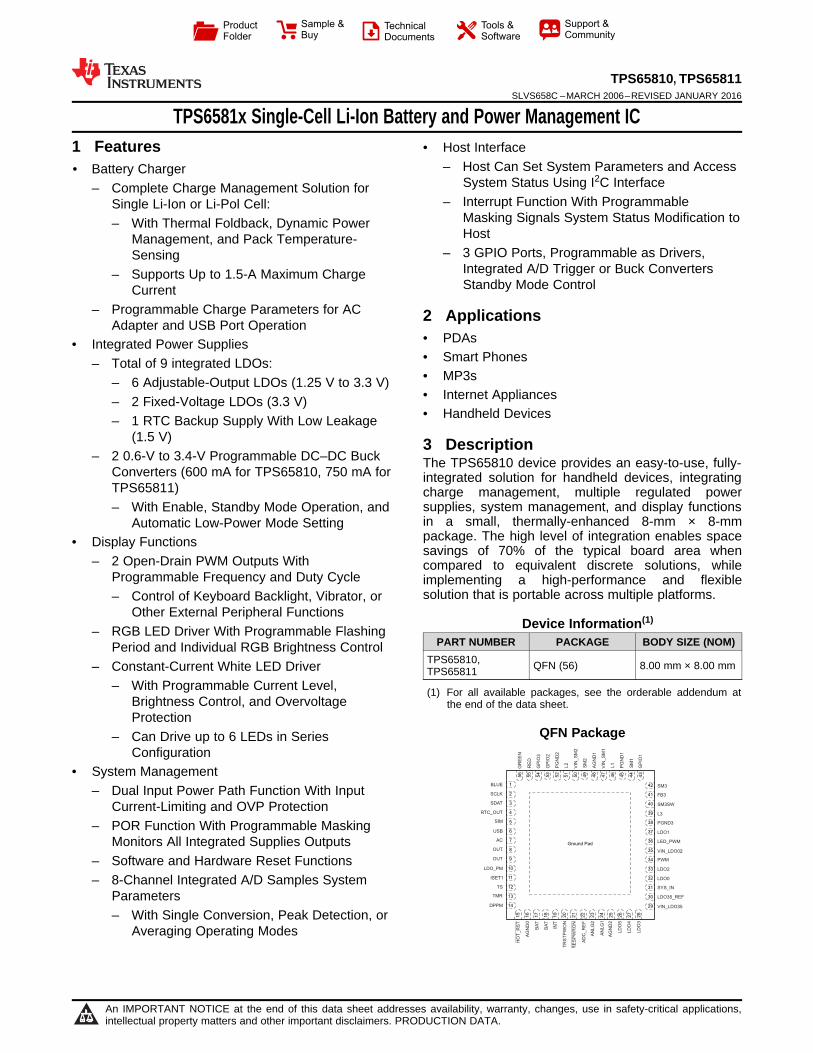
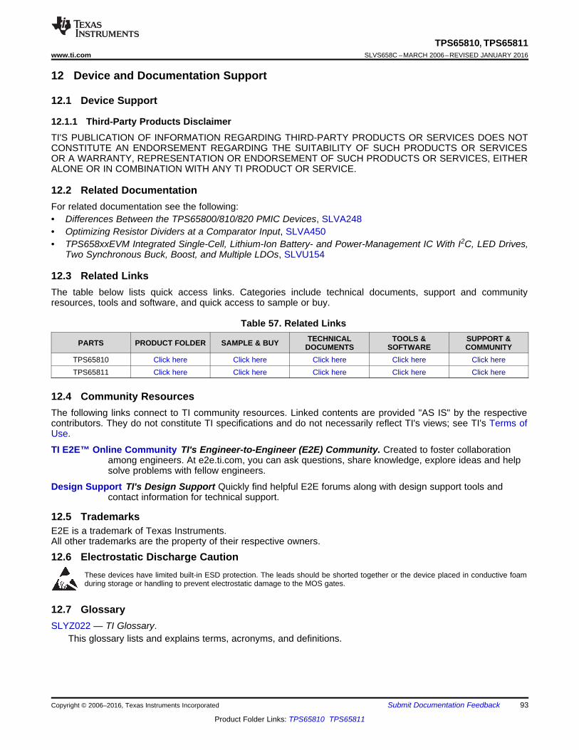
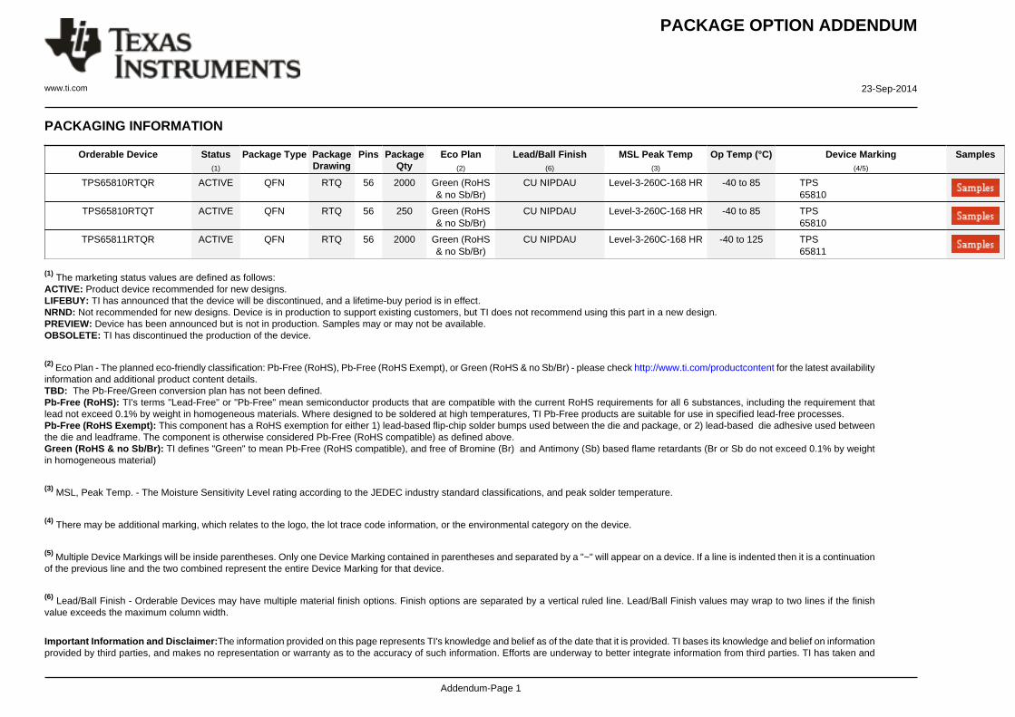
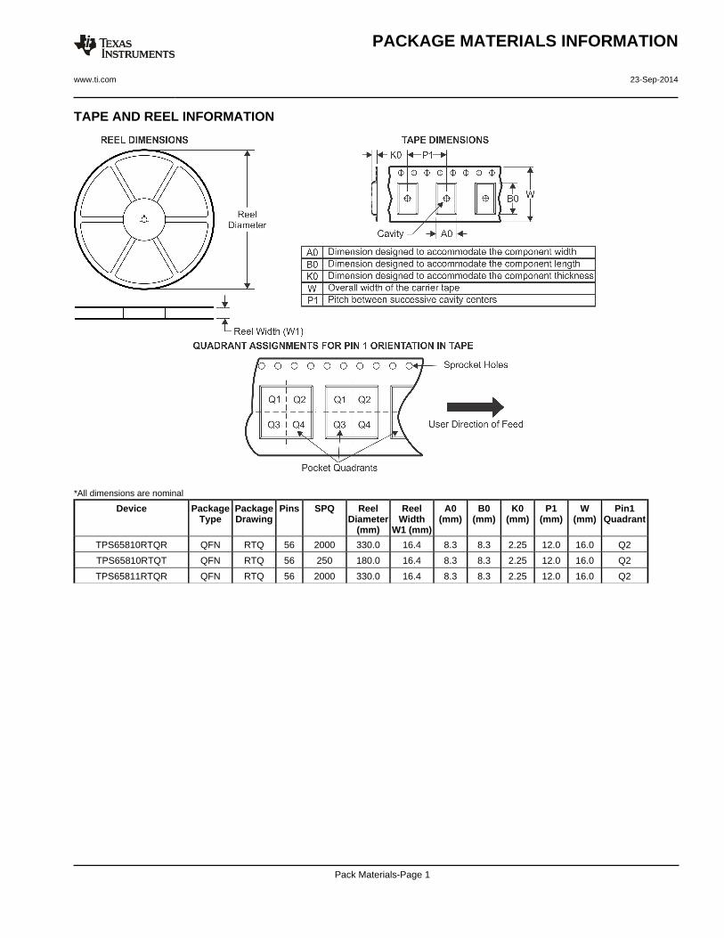
42 41 40 39 38 37 36 35 34 33 32 31 30 29 56 55 54 53 52 51 50 49 48 47 46 45 44 43 14 13 12 11 10 9 8 7 6 5 4 3 2 1 28 27 26 25 24 23 22 21 20 19 18 17 16 15 Ground Pad SYS_IN L1 SM1 PGND1 PGND2 SM2 L2 AGND0 SM3 FB3 L3 SM3SW OUT SIM OUT GPIO1 USB GPIO2 LDO_PM PWM AC RED BAT GREEN BAT BLUE TMR SCLK ISET1 SDAT DPPM INT TS RESPWRON RTC_OUT TRSTPWON HOT_RST LDO1 LDO0 LDO3 LDO35_REF VIN_LDO35 LDO4 ADC_REF AGND2 ANLG1 ANLG2 LDO5 GPIO3 AGND1 VIN_LDO02 PGND3 VIN_SM2 VIN_SM1 LED_PWM LDO2 Product Folder Sample & Buy Technical Documents Tools & Software Support & Community TPS65810, TPS65811 SLVS658C – MARCH 2006 – REVISED JANUARY 2016 TPS6581x Single-Cell Li-Ion Battery and Power Management IC 1 Features • Host Interface – Host Can Set System Parameters and Access 1• Battery Charger System Status Using I 2 C Interface – Complete Charge Management Solution for – Interrupt Function With Programmable Single Li-Ion or Li-Pol Cell: Masking Signals System Status Modification to – With Thermal Foldback, Dynamic Power Host Management, and Pack Temperature- – 3 GPIO Ports, Programmable as Drivers, Sensing Integrated A/D Trigger or Buck Converters – Supports Up to 1.5-A Maximum Charge Standby Mode Control Current – Programmable Charge Parameters for AC 2 Applications Adapter and USB Port Operation • PDAs • Integrated Power Supplies • Smart Phones – Total of 9 integrated LDOs: • MP3s – 6 Adjustable-Output LDOs (1.25 V to 3.3 V) • Internet Appliances – 2 Fixed-Voltage LDOs (3.3 V) • Handheld Devices – 1 RTC Backup Supply With Low Leakage (1.5 V) 3 Description – 2 0.6-V to 3.4-V Programmable DC–DC Buck The TPS65810 device provides an easy-to-use, fully- Converters (600 mA for TPS65810, 750 mA for integrated solution for handheld devices, integrating TPS65811) charge management, multiple regulated power supplies, system management, and display functions – With Enable, Standby Mode Operation, and in a small, thermally-enhanced 8-mm × 8-mm Automatic Low-Power Mode Setting package. The high level of integration enables space • Display Functions savings of 70% of the typical board area when – 2 Open-Drain PWM Outputs With compared to equivalent discrete solutions, while Programmable Frequency and Duty Cycle implementing a high-performance and flexible solution that is portable across multiple platforms. – Control of Keyboard Backlight, Vibrator, or Other External Peripheral Functions Device Information (1) – RGB LED Driver With Programmable Flashing PART NUMBER PACKAGE BODY SIZE (NOM) Period and Individual RGB Brightness Control TPS65810, QFN (56) 8.00 mm × 8.00 mm – Constant-Current White LED Driver TPS65811 – With Programmable Current Level, (1) For all available packages, see the orderable addendum at Brightness Control, and Overvoltage the end of the data sheet. Protection QFN Package – Can Drive up to 6 LEDs in Series Configuration • System Management – Dual Input Power Path Function With Input Current-Limiting and OVP Protection – POR Function With Programmable Masking Monitors All Integrated Supplies Outputs – Software and Hardware Reset Functions – 8-Channel Integrated A/D Samples System Parameters – With Single Conversion, Peak Detection, or Averaging Operating Modes 1 An IMPORTANT NOTICE at the end of this data sheet addresses availability, warranty, changes, use in safety-critical applications, intellectual property matters and other important disclaimers. PRODUCTION DATA.
Transcript
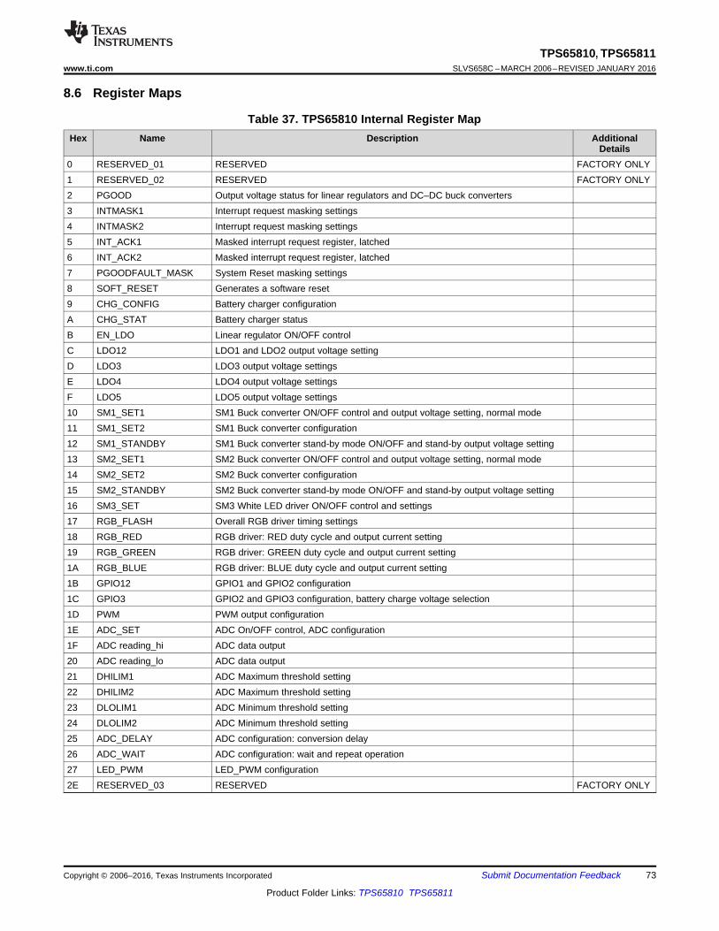
42
41
40
39
38
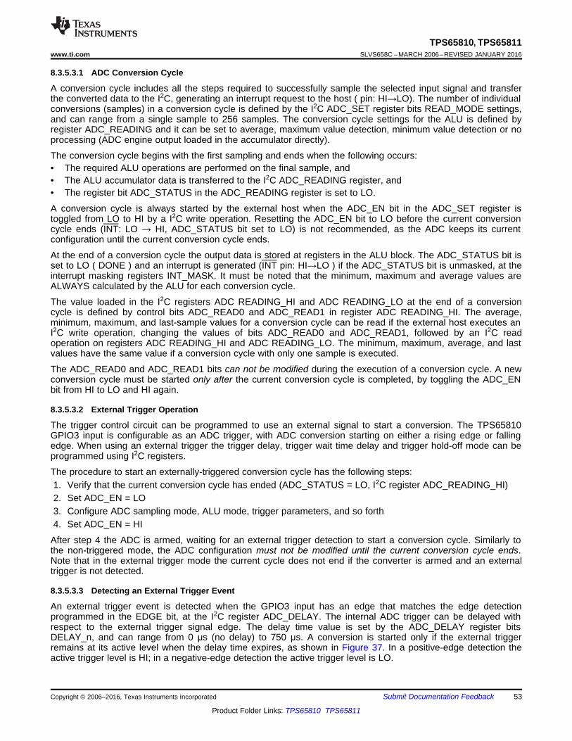
37
36
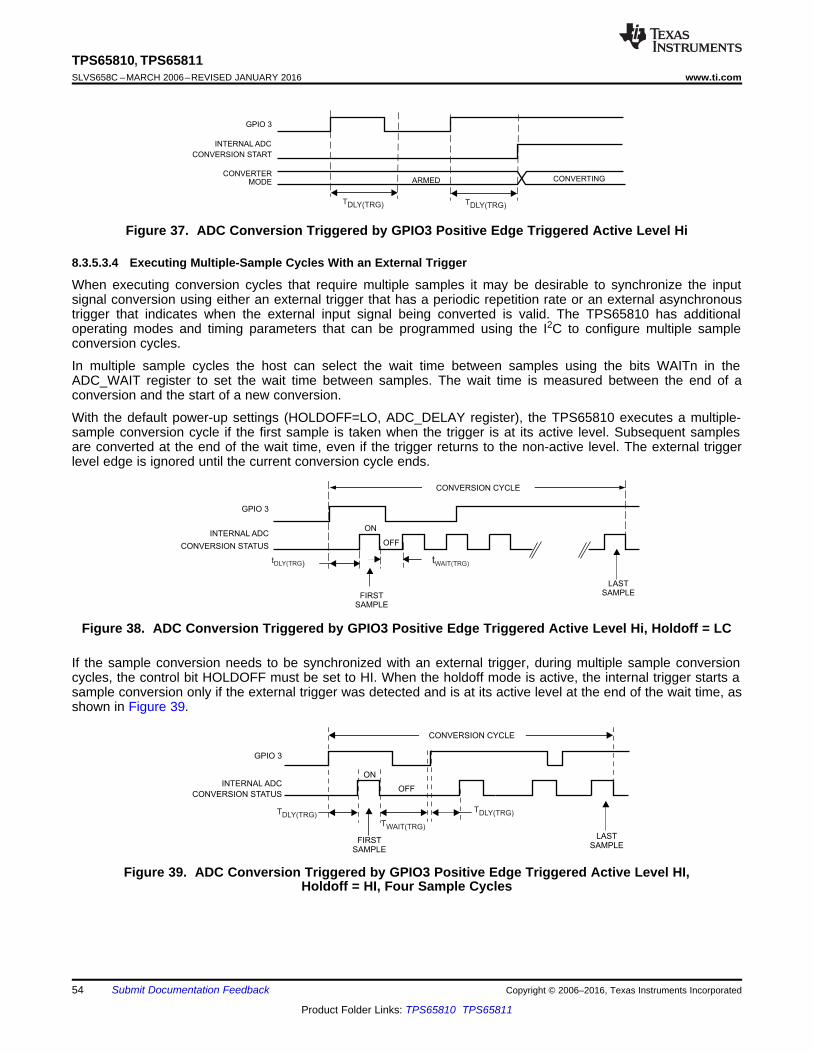
35
34
33
32
31
30
29
56
55
54
53
52
51
50
49
48
47
46
45
44
43
14
13
12
11
10
9
8
7
6
5
4
3
2
1
28
27
26
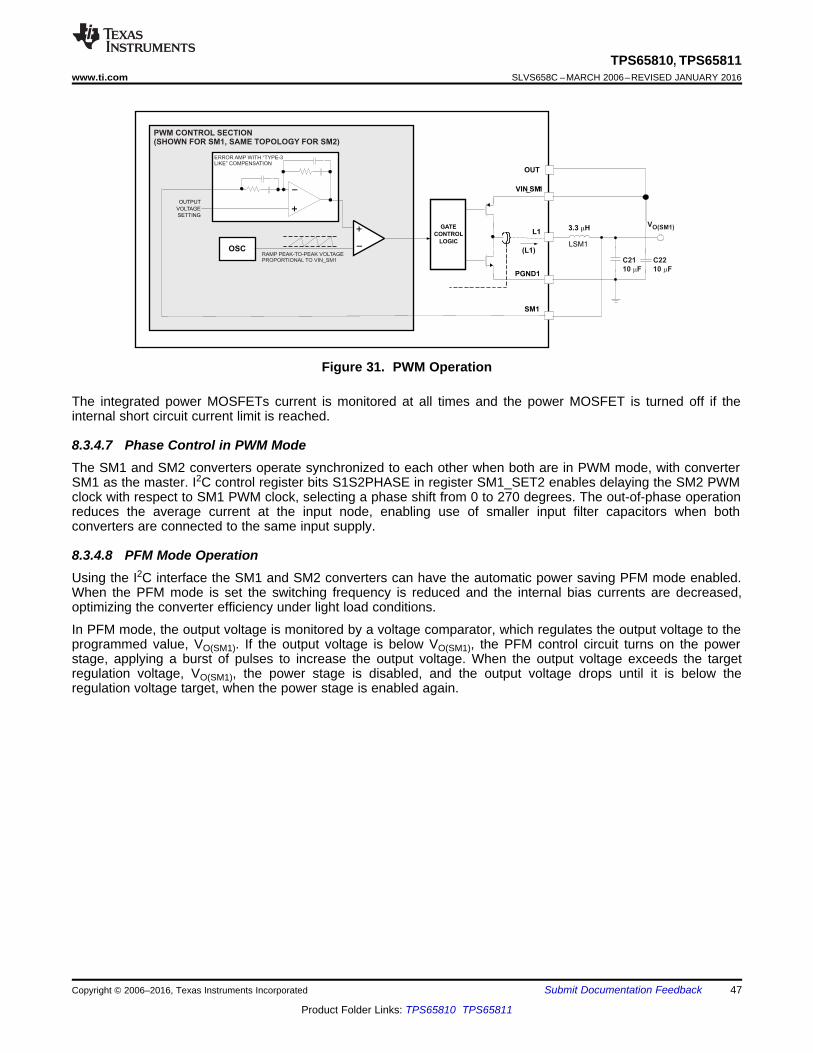
25
24
23
22
21
20
19
18
17
16
15
Ground Pad
SYS_IN
L1
SM
1
PG
ND
1
PG
ND
2
SM
2
L2
AG
ND
0
SM3
FB3
L3
SM3SW
OUT
SIM
OUT
GP
IO1
USB
GP
IO2
LDO_PM
PWM
AC
RE
D
BA
T
GR
EE
N
BA
T
BLUE
TMR
SCLK
ISET1
SDAT
DPPM
INT
TS
RE
SP
WR
ON
RTC_OUT
TR
ST
PW
ON
HO
T_
RS
T
LDO1
LDO0
LD
O3
LDO35_REF
VIN_LDO35
LD
O4
AD
C_
RE
F
AG
ND
2
AN
LG
1
AN
LG
2
LD
O5
GP
IO3
AG
ND
1
VIN_LDO02
PGND3
VIN
_S
M2
VIN
_S
M1
LED_PWM
LDO2
Product
Folder
Sample &Buy
Technical
Documents
Tools &
Software
Support &Community
TPS65810, TPS65811SLVS658C –MARCH 2006–REVISED JANUARY 2016
TPS6581x Single-Cell Li-Ion Battery and Power Management IC1 Features • Host Interface
– Host Can Set System Parameters and Access1• Battery Charger
System Status Using I2C Interface– Complete Charge Management Solution for– Interrupt Function With ProgrammableSingle Li-Ion or Li-Pol Cell:
Masking Signals System Status Modification to– With Thermal Foldback, Dynamic PowerHostManagement, and Pack Temperature-
– 3 GPIO Ports, Programmable as Drivers,SensingIntegrated A/D Trigger or Buck Converters– Supports Up to 1.5-A Maximum ChargeStandby Mode ControlCurrent
– Programmable Charge Parameters for AC 2 ApplicationsAdapter and USB Port Operation
• PDAs• Integrated Power Supplies• Smart Phones– Total of 9 integrated LDOs:• MP3s– 6 Adjustable-Output LDOs (1.25 V to 3.3 V)• Internet Appliances– 2 Fixed-Voltage LDOs (3.3 V)• Handheld Devices– 1 RTC Backup Supply With Low Leakage
(1.5 V) 3 Description– 2 0.6-V to 3.4-V Programmable DC–DC Buck The TPS65810 device provides an easy-to-use, fully-
Converters (600 mA for TPS65810, 750 mA for integrated solution for handheld devices, integratingTPS65811) charge management, multiple regulated power
supplies, system management, and display functions– With Enable, Standby Mode Operation, andin a small, thermally-enhanced 8-mm × 8-mmAutomatic Low-Power Mode Settingpackage. The high level of integration enables space• Display Functions savings of 70% of the typical board area when
– 2 Open-Drain PWM Outputs With compared to equivalent discrete solutions, whileProgrammable Frequency and Duty Cycle implementing a high-performance and flexible
solution that is portable across multiple platforms.– Control of Keyboard Backlight, Vibrator, orOther External Peripheral Functions
Device Information(1)– RGB LED Driver With Programmable Flashing
PART NUMBER PACKAGE BODY SIZE (NOM)Period and Individual RGB Brightness ControlTPS65810, QFN (56) 8.00 mm × 8.00 mm– Constant-Current White LED Driver TPS65811
– With Programmable Current Level, (1) For all available packages, see the orderable addendum atBrightness Control, and Overvoltage the end of the data sheet.Protection
QFN Package– Can Drive up to 6 LEDs in SeriesConfiguration
• System Management– Dual Input Power Path Function With Input
Current-Limiting and OVP Protection– POR Function With Programmable Masking
Monitors All Integrated Supplies Outputs– Software and Hardware Reset Functions– 8-Channel Integrated A/D Samples System
Parameters– With Single Conversion, Peak Detection, or
Averaging Operating Modes
1
An IMPORTANT NOTICE at the end of this data sheet addresses availability, warranty, changes, use in safety-critical applications,intellectual property matters and other important disclaimers. PRODUCTION DATA.
TPS65810, TPS65811www.ti.com SLVS658C –MARCH 2006–REVISED JANUARY 2016
5 Description (continued)If required, an external host can control the TPS65810 device through I2C interface with access to all integratedsystems. The I2C enables the setting of the output voltages, current thresholds, and operation modes. Theinternal registers have a complete set of status information, enabling easy diagnostics, and host-controlledhandling of fault conditions. The TPS65810 device can operate in standalone mode, with no external hostcontrol, if the internal power-up defaults are compatible with the system requirements.
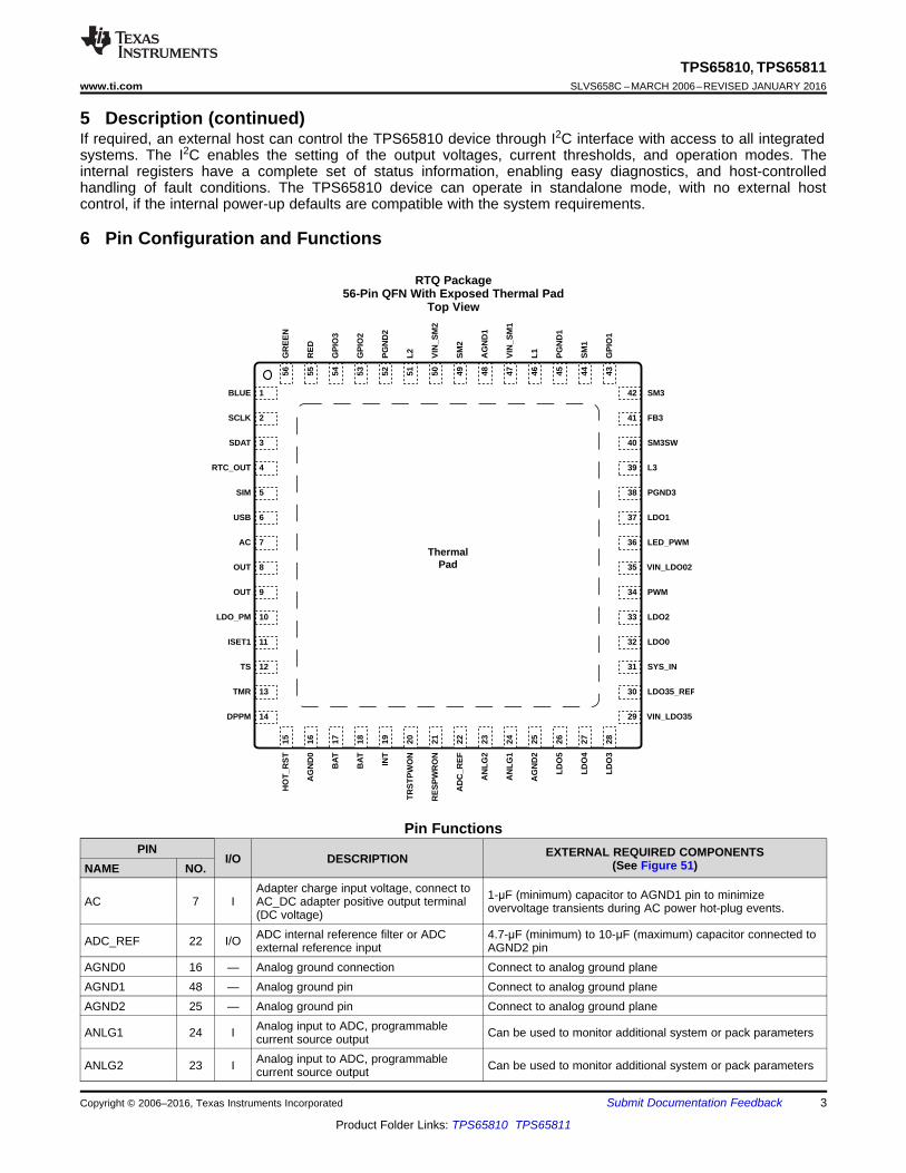
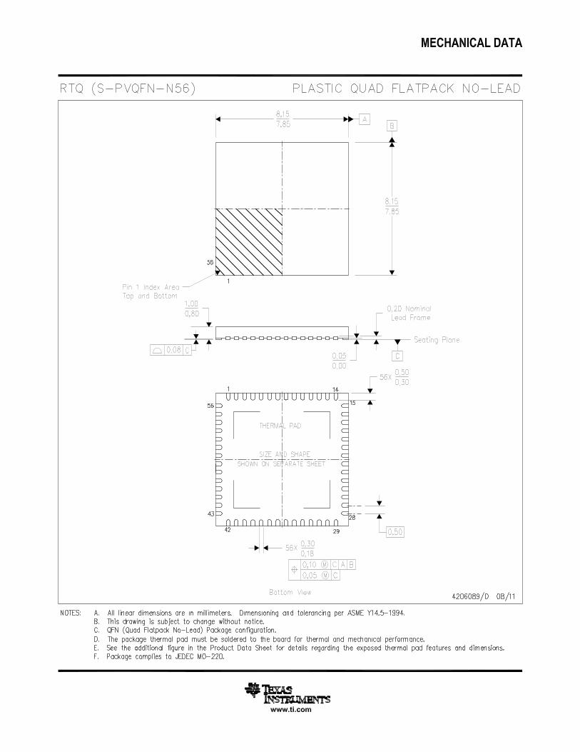
6 Pin Configuration and Functions
RTQ Package56-Pin QFN With Exposed Thermal Pad
Top View
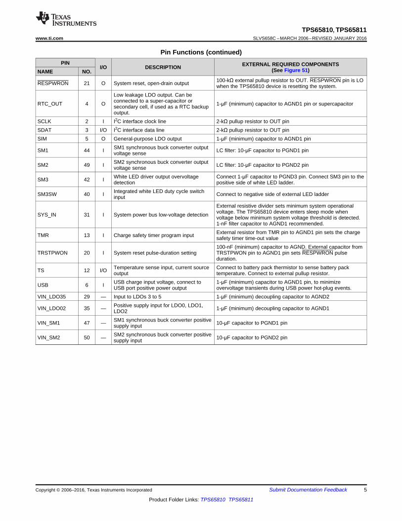
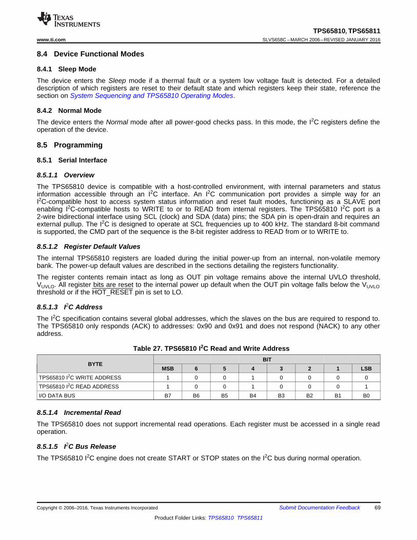
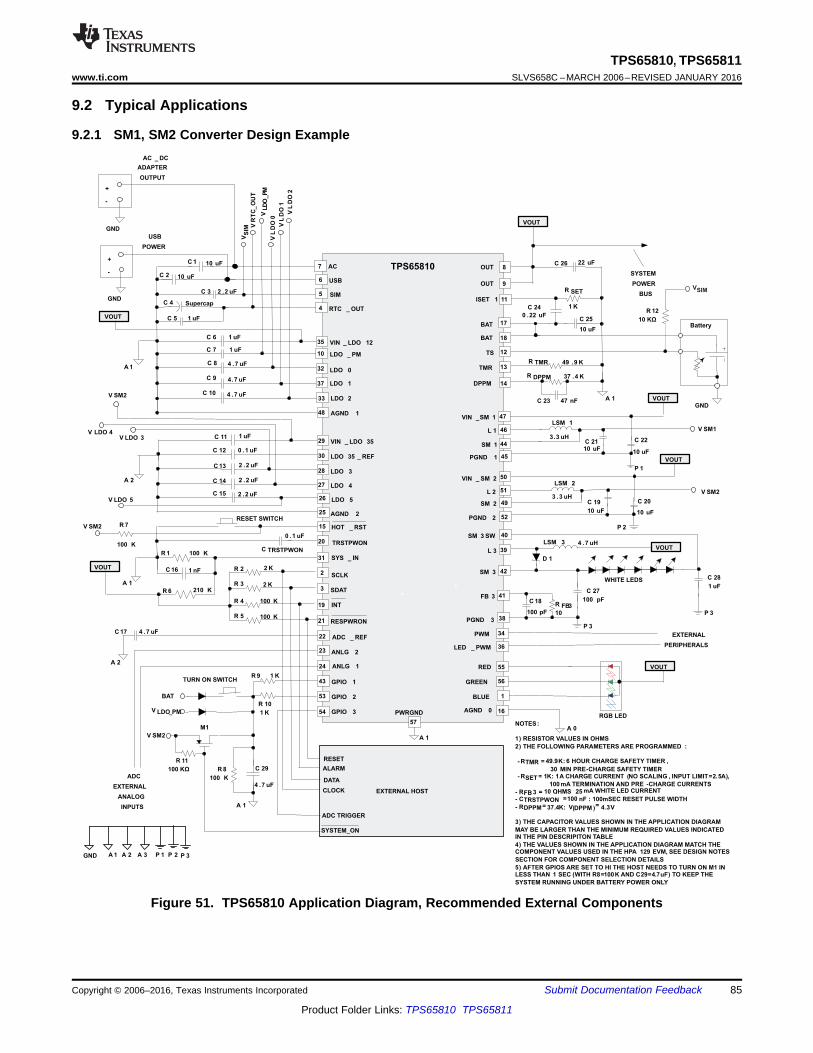
Pin FunctionsPIN EXTERNAL REQUIRED COMPONENTSI/O DESCRIPTION (See Figure 51)NAME NO.
Adapter charge input voltage, connect to 1-μF (minimum) capacitor to AGND1 pin to minimizeAC 7 I AC_DC adapter positive output terminal overvoltage transients during AC power hot-plug events.(DC voltage)ADC internal reference filter or ADC 4.7-μF (minimum) to 10-μF (maximum) capacitor connected toADC_REF 22 I/O external reference input AGND2 pin
AGND0 16 — Analog ground connection Connect to analog ground planeAGND1 48 — Analog ground pin Connect to analog ground planeAGND2 25 — Analog ground pin Connect to analog ground plane
Analog input to ADC, programmableANLG1 24 I Can be used to monitor additional system or pack parameterscurrent source outputAnalog input to ADC, programmableANLG2 23 I Can be used to monitor additional system or pack parameterscurrent source output
17 Connect to battery positive terminal. Connect a 10-μF capacitorBAT I/O Battery power (minimum) from BAT pin to AGND1 pin.18Programmable blue driver, open-drainBLUE 1 O Connect to BLUE input of RGB LEDoutput, current sink output when active.
External resistor from DPPM pin to AGND1 pin sets the DPPMDynamic power path management regulation threshold. 1-nF (minimum) capacitor to from DPPMDPPM 14 I set-point to AGND1 sets BAT to OUT short circuit blanking delay when
battery is hot-plugged into systemAn internal electrical connection exists between the exposed thermal pad and AGNDn pins of the device.
Exposed The exposed thermal pad must be connected to the same potential as the AGND1 pin on the printed-57 —thermal pad circuit-board. Do not use the thermal pad as the primary ground input for the device. AGNDn pins must beconnected to a clean ground plane at all times.
External resistor from FB3 pin to PGND3 pin sets LED peakWhite LED duty cycle switch output, LEDFB3 41 I/O current. Connect a 100-pF (minimum) filter capacitor to PGND3current setting pin.GPIO1 43 I/O General-purpose programmable I/O Power-up default: SM1 enable control, SM1 ON at GPIO1 = HI.GPIO2 53 I/O General-purpose programmable I/O Power-up default: SM2 enable control, SM2 ON at GPIO2 = HI.GPIO3 54 I/O General-purpose programmable I/O. Example: ADC conversion start trigger.
Programmable LED driver, open-drainGREEN 56 O Connect to GREEN input of RGB LEDoutput, current sink output when active.Hardware reset input, reset generated Connect to an external push-button switch. Connect to externalHOT_RST 15 I/O when connected to ground pullup resistor.
Connect 100-kΩ external pullup resistor between INT and OUTINT 19 O Interruption pin, open-drain output INT pin is LO when interrupt is requested by the TPS65810
device.Current set point when charging in automode with AC selected. Precharge and External resistor from ISET1 pin to AGND1 pin sets chargeISET1 11 I charge termination set point for all charge current valuemodesSM1 synchronous buck converterL1 46 O 3.3-μH inductor to SM1 pinpower-stage outputSM2 synchronous buck converterL2 51 O 3.3-μH inductor to SM2 pinpower-stage outputDrain of the integrated boost power-stageL3 39 O 4.7-μH inductor to OUT pin, external Schottky diode to SM3 pinswitch
LDO0 32 O LDO0 output, fixed voltage 1-μF (minimum) capacitor to AGND1LDO1 37 O LDO1 output 1-μF (minimum) capacitor to AGND1LDO2 33 O LDO2 output 1-μF (minimum) capacitor to AGND1LDO3 28 O LDO3 output 2.2-μF (minimum) capacitor to AGND2LDO35_REF 30 I Linear regulators LDO3-5 reference filter 100-nF capacitor to AGND2LDO4 27 O LDO4 output 2.2-μF (minimum) capacitor to AGND2LDO5 26 O LDO5 output 2.2-μF (minimum) capacitor to AGND2LDO_PM 10 O General-purpose LDO output 1-μF (minimum) capacitor to AGND1 pinLED_PWM 36 O PWM driver output, open-drain Can be used to drive a keyboard backlight LED
8 Power-path output. Connect to systemOUT O 10-μF capacitor to AGND1 pinmain power rail (system power bus)9PGND1 45 SM1 synchronous buck converter power— Connect to power ground planegroundPGND2 52PGND3 38 — White LED driver power ground input. Connect to a power ground planePWM 34 O PWM driver output, open-drain Can be used to drive a vibrator or other external functions
Programmable LED driver, open-drainRED 55 O Connect to RED input of RGB LEDoutput, current sink output when active
100-kΩ external pullup resistor to OUT. RESPWRON pin is LORESPWRON 21 O System reset, open-drain output when the TPS65810 device is resetting the system.Low leakage LDO output. Can beconnected to a super-capacitor orRTC_OUT 4 O 1-μF (minimum) capacitor to AGND1 pin or supercapacitorsecondary cell, if used as a RTC backupoutput.
SCLK 2 I I2C interface clock line 2-kΩ pullup resistor to OUT pinSDAT 3 I/O I2C interface data line 2-kΩ pullup resistor to OUT pinSIM 5 O General-purpose LDO output 1-μF (minimum) capacitor to AGND1 pin
SM1 synchronous buck converter outputSM1 44 I LC filter: 10-μF capacitor to PGND1 pinvoltage senseSM2 synchronous buck converter outputSM2 49 I LC filter: 10-μF capacitor to PGND2 pinvoltage senseWhite LED driver output overvoltage Connect 1-μF capacitor to PGND3 pin. Connect SM3 pin to theSM3 42 I detection positive side of white LED ladder.Integrated white LED duty cycle switchSM3SW 40 I Connect to negative side of external LED ladderinput
External resistive divider sets minimum system operationalvoltage. The TPS65810 device enters sleep mode whenSYS_IN 31 I System power bus low-voltage detection voltage below minimum system voltage threshold is detected.1-nF filter capacitor to AGND1 recommended.External resistor from TMR pin to AGND1 pin sets the chargeTMR 13 I Charge safety timer program input safety timer time-out value100-nF (minimum) capacitor to AGND. External capacitor from
TRSTPWON 20 I System reset pulse-duration setting TRSTPWON pin to AGND1 pin sets RESPWRON pulseduration.
Temperature sense input, current source Connect to battery pack thermistor to sense battery packTS 12 I/O output temperature. Connect to external pullup resistor.USB charge input voltage, connect to 1-μF (minimum) capacitor to AGND1 pin, to minimizeUSB 6 I USB port positive power output overvoltage transients during USB power hot-plug events.
VIN_LDO35 29 — Input to LDOs 3 to 5 1-μF (minimum) decoupling capacitor to AGND2Positive supply input for LDO0, LDO1,VIN_LDO02 35 — 1-μF (minimum) decoupling capacitor to AGND1LDO2SM1 synchronous buck converter positiveVIN_SM1 47 — 10-μF capacitor to PGND1 pinsupply inputSM2 synchronous buck converter positiveVIN_SM2 50 — 10-μF capacitor to PGND2 pinsupply input
TPS65810, TPS65811SLVS658C –MARCH 2006–REVISED JANUARY 2016 www.ti.com
7 Specifications
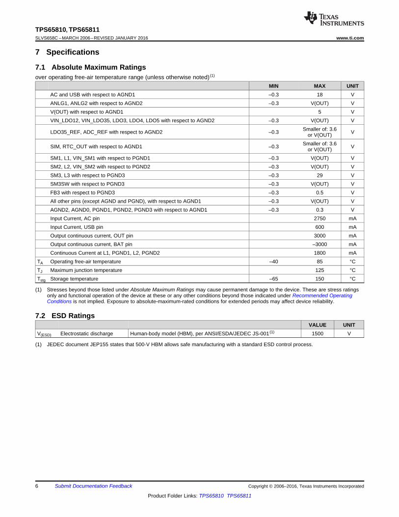
7.1 Absolute Maximum Ratingsover operating free-air temperature range (unless otherwise noted) (1)
MIN MAX UNITAC and USB with respect to AGND1 –0.3 18 VANLG1, ANLG2 with respect to AGND2 –0.3 V(OUT) VV(OUT) with respect to AGND1 5 VVIN_LDO12, VIN_LDO35, LDO3, LDO4, LDO5 with respect to AGND2 –0.3 V(OUT) V
Smaller of: 3.6LDO35_REF, ADC_REF with respect to AGND2 –0.3 Vor V(OUT)Smaller of: 3.6SIM, RTC_OUT with respect to AGND1 –0.3 Vor V(OUT)
SM1, L1, VIN_SM1 with respect to PGND1 –0.3 V(OUT) VSM2, L2, VIN_SM2 with respect to PGND2 –0.3 V(OUT) VSM3, L3 with respect to PGND3 –0.3 29 VSM3SW with respect to PGND3 –0.3 V(OUT) VFB3 with respect to PGND3 –0.3 0.5 VAll other pins (except AGND and PGND), with respect to AGND1 –0.3 V(OUT) VAGND2, AGND0, PGND1, PGND2, PGND3 with respect to AGND1 –0.3 0.3 VInput Current, AC pin 2750 mAInput Current, USB pin 600 mAOutput continuous current, OUT pin 3000 mAOutput continuous current, BAT pin –3000 mAContinuous Current at L1, PGND1, L2, PGND2 1800 mA
TA Operating free-air temperature –40 85 °CTJ Maximum junction temperature 125 °CTstg Storage temperature –65 150 °C
(1) Stresses beyond those listed under Absolute Maximum Ratings may cause permanent damage to the device. These are stress ratingsonly and functional operation of the device at these or any other conditions beyond those indicated under Recommended OperatingConditions is not implied. Exposure to absolute-maximum-rated conditions for extended periods may affect device reliability.
7.2 ESD RatingsVALUE UNIT
V(ESD) Electrostatic discharge Human-body model (HBM), per ANSI/ESDA/JEDEC JS-001 (1) 1500 V
(1) JEDEC document JEP155 states that 500-V HBM allows safe manufacturing with a standard ESD control process.
TPS65810, TPS65811www.ti.com SLVS658C –MARCH 2006–REVISED JANUARY 2016
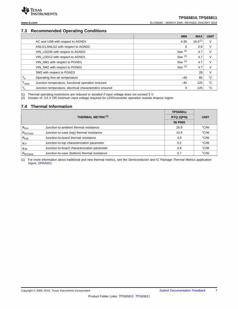
7.3 Recommended Operating ConditionsMIN MAX UNIT
AC and USB with respect to AGND1 4.35 16.5 (1) VANLG1,ANLG2 with respect to AGND2 0 2.6 VVIN_LDO35 with respect to AGND2 See (2) 4.7 VVIN_LDO12 with respect to AGND1 See (2) 4.7 VVIN_SM1 with respect to PGND1 See (2) 4.7 VVIN_SM2 with respect to PGND2 See (2) 4.7 VSM3 with respect to PGND3 28 V
TA Operating free-air temperature –40 85 °CTJ(op) Junction temperature, functional operation ensured –40 125 °CTJ Junction temperature, electrical characteristics ensured 0 125 °C
(1) Thermal operating restrictions are reduced or avoided if input voltage does not exceed 5 V.(2) Greater of: 3.6 V OR minimum input voltage required for LDO/converter operation outside dropout region.
TPS65810, TPS65811SLVS658C –MARCH 2006–REVISED JANUARY 2016 www.ti.com
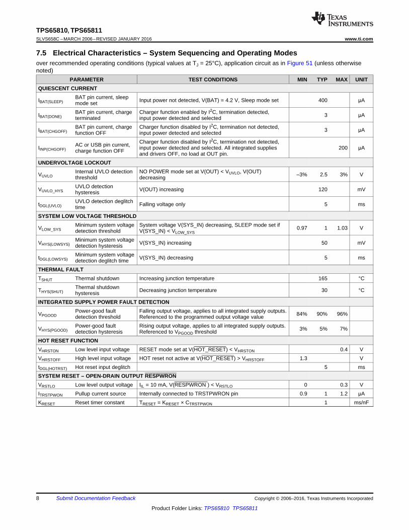
7.5 Electrical Characteristics – System Sequencing and Operating Modesover recommended operating conditions (typical values at TJ = 25°C), application circuit as in Figure 51 (unless otherwisenoted)
PARAMETER TEST CONDITIONS MIN TYP MAX UNITQUIESCENT CURRENT
BAT pin current, sleepIBAT(SLEEP) Input power not detected, V(BAT) = 4.2 V, Sleep mode set 400 μAmode setBAT pin current, charge Charger function enabled by I2C, termination detected,IBAT(DONE) 3 μAterminated input power detected and selectedBAT pin current, charge Charger function disabled by I2C, termination not detected,IBAT(CHGOFF) 3 μAfunction OFF input power detected and selected
Charger function disabled by I2C, termination not detected,AC or USB pin current,IINP(CHGOFF) input power detected and selected. All integrated supplies 200 μAcharge function OFF and drivers OFF, no load at OUT pin.UNDERVOLTAGE LOCKOUT
Internal UVLO detection NO POWER mode set at V(OUT) < VUVLO, V(OUT)VUVLO –3% 2.5 3% Vthreshold decreasingUVLO detectionVUVLO_HYS V(OUT) increasing 120 mVhysteresisUVLO detection deglitchtDGL(UVLO) Falling voltage only 5 mstime
SYSTEM LOW VOLTAGE THRESHOLDMinimum system voltage System voltage V(SYS_IN) decreasing, SLEEP mode set ifVLOW_SYS 0.97 1 1.03 Vdetection threshold V(SYS_IN) < VLOW_SYS
Minimum system voltageVHYS(LOWSYS) V(SYS_IN) increasing 50 mVdetection hysteresisMinimum system voltagetDGL(LOWSYS) V(SYS_IN) decreasing 5 msdetection deglitch time
THERMAL FAULTTSHUT Thermal shutdown Increasing junction temperature 165 °C
Thermal shutdownTHYS(SHUT) Decreasing junction temperature 30 °ChysteresisINTEGRATED SUPPLY POWER FAULT DETECTION
Power-good fault Falling output voltage, applies to all integrated supply outputs.VPGOOD 84% 90% 96%detection threshold Referenced to the programmed output voltage valuePower-good fault Rising output voltage, applies to all integrated supply outputs.VHYS(PGOOD) 3% 5% 7%detection hysteresis Referenced to VPGOOD threshold
HOT RESET FUNCTIONVHRSTON Low level input voltage RESET mode set at V(HOT_RESET) < VHRSTON 0.4 VVHRSTOFF High level input voltage HOT reset not active at V(HOT_RESET) > VHRSTOFF 1.3 VtDGL(HOTRST) Hot reset input deglitch 5 msSYSTEM RESET – OPEN-DRAIN OUTPUT RESPWRONVRSTLO Low level output voltage IIL = 10 mA, V(RESPWRON ) < VRSTLO 0 0.3 VITRSTPWON Pullup current source Internally connected to TRSTPWRON pin 0.9 1 1.2 μAKRESET Reset timer constant TRESET = KRESET × CTRSTPWON 1 ms/nF
TPS65810, TPS65811www.ti.com SLVS658C –MARCH 2006–REVISED JANUARY 2016
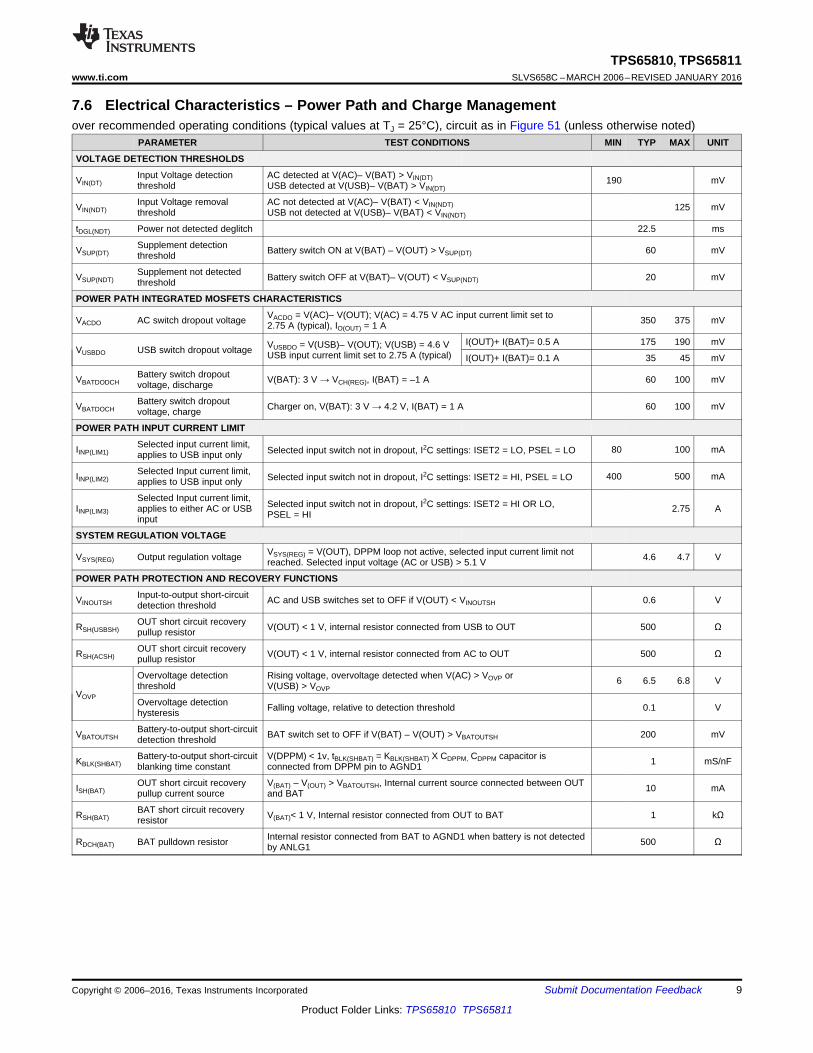
7.6 Electrical Characteristics – Power Path and Charge Managementover recommended operating conditions (typical values at TJ = 25°C), circuit as in Figure 51 (unless otherwise noted)
PARAMETER TEST CONDITIONS MIN TYP MAX UNIT
VOLTAGE DETECTION THRESHOLDS
Input Voltage detection AC detected at V(AC)– V(BAT) > VIN(DT)VIN(DT) 190 mVthreshold USB detected at V(USB)– V(BAT) > VIN(DT)
Input Voltage removal AC not detected at V(AC)– V(BAT) < VIN(NDT)VIN(NDT) 125 mVthreshold USB not detected at V(USB)– V(BAT) < VIN(NDT)
tDGL(NDT) Power not detected deglitch 22.5 ms
Supplement detectionVSUP(DT) Battery switch ON at V(BAT) – V(OUT) > VSUP(DT) 60 mVthreshold
Supplement not detectedVSUP(NDT) Battery switch OFF at V(BAT)– V(OUT) < VSUP(NDT) 20 mVthreshold
POWER PATH INTEGRATED MOSFETS CHARACTERISTICS
VACDO = V(AC)– V(OUT); V(AC) = 4.75 V AC input current limit set toVACDO AC switch dropout voltage 350 375 mV2.75 A (typical), IO(OUT) = 1 A
I(OUT)+ I(BAT)= 0.5 A 175 190 mVVUSBDO = V(USB)– V(OUT); V(USB) = 4.6 VVUSBDO USB switch dropout voltage USB input current limit set to 2.75 A (typical) I(OUT)+ I(BAT)= 0.1 A 35 45 mV
Battery switch dropoutVBATDODCH V(BAT): 3 V → VCH(REG), I(BAT) = –1 A 60 100 mVvoltage, discharge
Battery switch dropoutVBATDOCH Charger on, V(BAT): 3 V → 4.2 V, I(BAT) = 1 A 60 100 mVvoltage, charge
POWER PATH INPUT CURRENT LIMIT
Selected input current limit,IINP(LIM1) 80 100 mASelected input switch not in dropout, I2C settings: ISET2 = LO, PSEL = LOapplies to USB input only
Selected Input current limit,IINP(LIM2) 400 500 mASelected input switch not in dropout, I2C settings: ISET2 = HI, PSEL = LOapplies to USB input only
Selected Input current limit, Selected input switch not in dropout, I2C settings: ISET2 = HI OR LO,IINP(LIM3) applies to either AC or USB 2.75 APSEL = HIinput
SYSTEM REGULATION VOLTAGE
VSYS(REG) = V(OUT), DPPM loop not active, selected input current limit notVSYS(REG) Output regulation voltage 4.6 4.7 Vreached. Selected input voltage (AC or USB) > 5.1 V
POWER PATH PROTECTION AND RECOVERY FUNCTIONS
Input-to-output short-circuitVINOUTSH AC and USB switches set to OFF if V(OUT) < VINOUTSH 0.6 Vdetection threshold
OUT short circuit recoveryRSH(USBSH) V(OUT) < 1 V, internal resistor connected from USB to OUT 500 Ωpullup resistor
OUT short circuit recoveryRSH(ACSH) V(OUT) < 1 V, internal resistor connected from AC to OUT 500 Ωpullup resistor
Overvoltage detection Rising voltage, overvoltage detected when V(AC) > VOVP or 6 6.5 6.8 Vthreshold V(USB) > VOVPVOVP
Overvoltage detection Falling voltage, relative to detection threshold 0.1 Vhysteresis
Battery-to-output short-circuitVBATOUTSH BAT switch set to OFF if V(BAT) – V(OUT) > VBATOUTSH 200 mVdetection threshold
Battery-to-output short-circuit V(DPPM) < 1v, tBLK(SHBAT) = KBLK(SHBAT) X CDPPM, CDPPM capacitor isKBLK(SHBAT) 1 mS/nFblanking time constant connected from DPPM pin to AGND1
OUT short circuit recovery V(BAT) – V(OUT) > VBATOUTSH, Internal current source connected between OUTISH(BAT) 10 mApullup current source and BAT
BAT short circuit recoveryRSH(BAT) V(BAT)< 1 V, Internal resistor connected from OUT to BAT 1 kΩresistor
Internal resistor connected from BAT to AGND1 when battery is not detectedRDCH(BAT) BAT pulldown resistor 500 Ωby ANLG1
IQ(SM2) = I(VIN_ SM2), no output load, not switching 10IQ(SM2) Quiescent current for SM2 μA
0.1SM2 OFF, set through I2C
Vin = 4.2 V, Vout = 1.24 V (TPS65810) 600IO(SM2) Output current range mA
Vin = 4.2 V, Vout = 1.24 V (TPS65811) 750
Available output voltages:VO(SM2)TYP = 1 V to 3.4 V,Output voltage, selectable through I2C, stand-by OFFadjustable in 80-mV steps
VAvailable output voltages:
VO(SM2) = VSBY(SM2), Output voltage range, stand-by ON VSBY(SM2) = 1 V to 3.4 V,adjustable in 80-mV steps
Total accuracy, VO(SM2)TYP = VSM2(SBY) = 1.8 V,VO(SM2) Output voltage V(VIN_SM2) = greater of [3.0 V or (VO(SM2) + 0.3 V)] –3% 3%to 4.7 V; 0 mA ≤ IO(SM2) ≤ 600 mA
Line regulation, V(VIN_SM2) = greater of[3 V or (VO(SM2) + 0.3 V)] 0.027 %/Vto 4.7 V; 0 mA ≤ IO(SM2) ≤ 600 mA
Load regulation, V(VIN_SM2) = 4.7 V, 0.139 %/AIO(SM2): 60 mA → 540 mA
Converter OFF→ON, VO(SM2) : 5% → 95% of targettSS(SM2) Soft-start ramp time 750 μsvalue
GPIO2 pin programmed as SM2 converter enabletDLY(SM2) Converter turnon delay 170 μscontrol. Measured from V(GPIO2): LO → HI
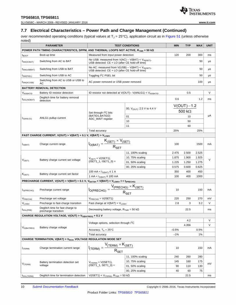
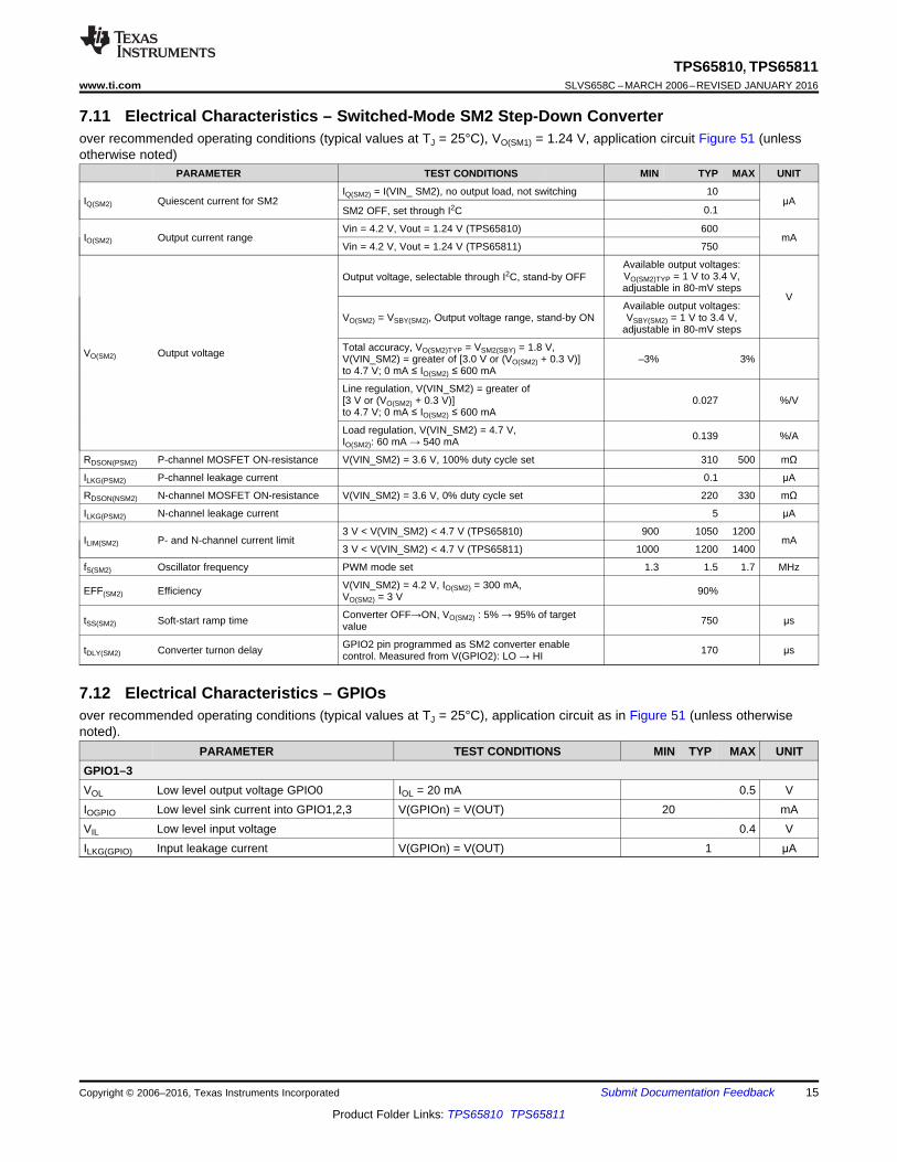
7.12 Electrical Characteristics – GPIOsover recommended operating conditions (typical values at TJ = 25°C), application circuit as in Figure 51 (unless otherwisenoted).
PARAMETER TEST CONDITIONS MIN TYP MAX UNITGPIO1–3VOL Low level output voltage GPIO0 IOL = 20 mA 0.5 VIOGPIO Low level sink current into GPIO1,2,3 V(GPIOn) = V(OUT) 20 mAVIL Low level input voltage 0.4 VILKG(GPIO) Input leakage current V(GPIOn) = V(OUT) 1 μA
TPS65810, TPS65811www.ti.com SLVS658C –MARCH 2006–REVISED JANUARY 2016
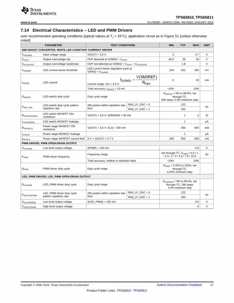
7.14 Electrical Characteristics – LED and PWM Driversover recommended operating conditions (typical values at TJ = 25°C), application circuit as in Figure 51 (unless otherwisenoted)
PARAMETER TEST CONDITIONS MIN TYP MAX UNIT
SM3 BOOST CONVERTER, WHITE LED CONSTANT CURRENT DRIVER
VVIN(SM3) Input voltage range V(OUT) = 3.3 V 3 4.7 V
VOVP3 Output overvoltage trip OVP detected at V(SM3) > VOVP3 26.5 29 30 V
VHYS(OVP3) Output overvoltage hysteresis OVP not detected at V(SM3) < VOVP3 – VHYS(OVP3) 1.8 V
LED current below regulation point atVSM3REF LED current-sense threshold 244 252 260 mVV(FB3) < VSM3REF
0 25 mAIO(SM3) LED current Current range, Vin = 3.3 V,
Total accuracy, IO(SM3) = 10 mA –10% 10%
DSM3SW = 0% to 99.6%, setDSM3SW LED-switch duty cycle Duty cycle range through I2C,
256 steps, 0.4% minimum step
SM3_LF_OSC = 0 122LED-switch duty cycle pattern 256 pulses within repetition rateFREP_SM3 Hzrepetition rate time SM3_LF_OSC = 1 183
LED switch MOSFET ON-RDSON(SM3SW) V(OUT) = 3.6 V; I(SM3SW) = 20 mA 1 2 Ωresistance
ILKG(SM3SW) LED switch MOSFET leakage 1 μA
Power stage MOSFET ON-RDSON(L3) V(OUT) = 3.6 V; I(L3) = 200 mA 300 600 mΩresistance
ILKG(L3) Power stage MOSFET leakage 1 μA
IMAX(L3) Power stage MOSFET current limit 3 V < V(OUT) < 4.7 V 400 500 600 mA
PWM DRIVER, PWM OPEN-DRAIN OUTPUT
VOL(PWM) Low level output voltage I(PWM) = 150 mA 0.5 V
Set through I2C, FPWM = 0.5 / 1Frequency range Hz/ 1.5 / 2 / 3 / 4.5 / 7.8 / 15.6FPWM PWM driver frequencyTotal accuracy, relative to selected value –20% 20%
DPWM = 6.25% to 100%, setDPWM PWM driver duty cycle Duty cycle range through I2C,
6.25% minimum step
LED_PWM DRIVER, LED_PWM OPEN-DRAIN OUTPUT
DLEDPWM = 0% to 99.6%, setDLEDPWM LED_PWM driver duty cycle Duty cycle range through I2C, 256 steps
0.4% minimum step
SM3_LF_OSC = 0 122LED_PWM driver duty cycle 256 pulses within repetition rateFREP(LEDPWM) Hzpattern repetition rate time SM3_LF_OSC = 1 180
VOL(LEDPWM) Low level output voltage I(LED_PWM) = 150 mA 0.5 V
TPS65810, TPS65811SLVS658C –MARCH 2006–REVISED JANUARY 2016 www.ti.com
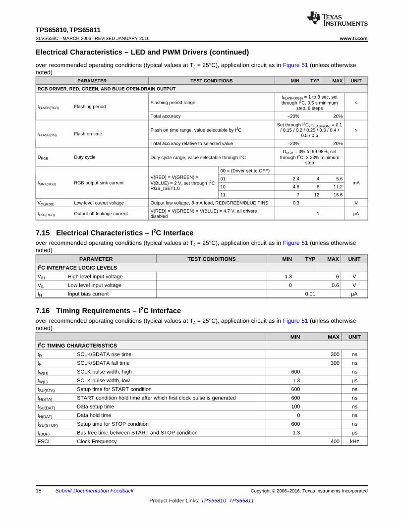
Electrical Characteristics – LED and PWM Drivers (continued)over recommended operating conditions (typical values at TJ = 25°C), application circuit as in Figure 51 (unless otherwisenoted)
PARAMETER TEST CONDITIONS MIN TYP MAX UNIT
RGB DRIVER, RED, GREEN, AND BLUE OPEN-DRAIN OUTPUT
tFLASH(RGB) = 1 to 8 sec, setFlashing period range sthrough I2C, 0.5 s minimum
tFLASH(RGB) Flashing period step, 8 steps
Total accuracy –20% 20%
Set through I2C, tFLASH(ON) = 0.1sFlash on time range, value selectable by I2C / 0.15 / 0.2 / 0.25 / 0.3 / 0.4 /
tFLASH(ON) Flash on time 0.5 / 0.6
Total accuracy relative to selected value –20% 20%
DRGB = 0% to 99.98%, setDRGB Duty cycle Duty cycle range, value selectable through I2C through I2C, 3.23% minimum
step
00 = (Driver set to OFF)V(RED) = V(GREEN) = 01 2.4 4 5.6
ISINK(RGB) RGB output sink current mAV(BLUE) = 2 V, set through I2C10 4.8 8 11.2RGB_ISET1,011 7 12 16.6
VOL(RGB) Low-level output voltage Output low voltage, 8-mA load, RED/GREEN/BLUE PINS 0.3 V
V(RED) = V(GREEN) = V(BLUE) = 4.7 V, all driversILKG(RGB) Output off leakage current 1 μAdisabled
7.15 Electrical Characteristics – I2C Interfaceover recommended operating conditions (typical values at TJ = 25°C), application circuit as in Figure 51 (unless otherwisenoted)
PARAMETER TEST CONDITIONS MIN TYP MAX UNITI2C INTERFACE LOGIC LEVELSVIH High level input voltage 1.3 6 VVIL Low level input voltage 0 0.6 VIH Input bias current 0.01 μA
7.16 Timing Requirements – I2C Interfaceover recommended operating conditions (typical values at TJ = 25°C), application circuit as in Figure 51 (unless otherwisenoted)
MIN MAX UNITI2C TIMING CHARACTERISTICStR SCLK/SDATA rise time 300 nstF SCLK/SDATA fall time 300 nstW(H) SCLK pulse width, high 600 nstW(L) SCLK pulse width, low 1.3 μstSU(STA) Setup time for START condition 600 nstH(STA) START condition hold time after which first clock pulse is generated 600 nstSU(DAT) Data setup time 100 nstH(DAT) Data hold time 0 nstSU(STOP) Setup time for STOP condition 600 nst(BUF) Bus free time between START and STOP condition 1.3 μsFSCL Clock Frequency 400 kHz
TPS65810, TPS65811www.ti.com SLVS658C –MARCH 2006–REVISED JANUARY 2016
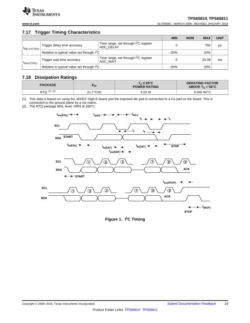
7.17 Trigger Timing CharacteristicsMIN NOM MAX UNIT
Time range, set through I2C registerTrigger delay time accuracy 0 750 µsADC_DELAYtDELAY(TRG)Relative to typical value set through I2C –20% 20%
Time range, set through I2C registerTrigger wait time accuracy 0 20.48 msADC_WAITtWAIT(TRG)Relative to typical value set through I2C –20% 20%
7.18 Dissipation RatingsTA ≤ 55°C DERATING FACTORPACKAGE θJA POWER RATING ABOVE TA = 55°C
RTQ (1) (2) 21.7°C/W 3.22 W 0.046 W/°C
(1) This data is based on using the JEDEC High-K board and the exposed die pad is connected to a Cu pad on the board. This isconnected to the ground plane by a via matrix.
AGND 0, AGND 1 AND AGND 2PINS SHORTED TO EACH OTHER INSIDE TPS 65800. ALL AGND PINS ARE INTERNALLY CONNECTED TO
THE TPS 65800 THERMAL PAD AND SUBSTRATE .
PGND1, PGND 3 AND PGND 3PINS ARE NOT CONNECTED TO EACH OTHER OR TO THE TPS 65800 SUBSTRATE / POWER PAD
DISPLAY AND I /OOUT
TPS65810, TPS65811www.ti.com SLVS658C –MARCH 2006–REVISED JANUARY 2016
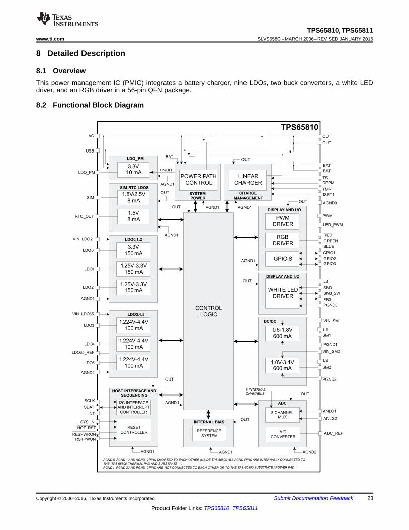
8 Detailed Description
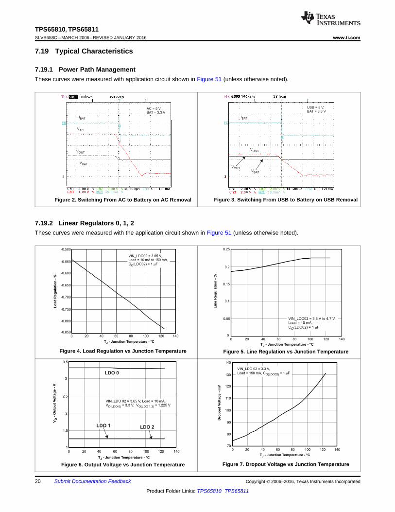
8.1 OverviewThis power management IC (PMIC) integrates a battery charger, nine LDOs, two buck converters, a white LEDdriver, and an RGB driver in a 56-pin QFN package.
TPS65810, TPS65811SLVS658C –MARCH 2006–REVISED JANUARY 2016 www.ti.com
8.3 Feature Description
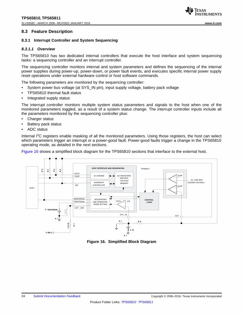
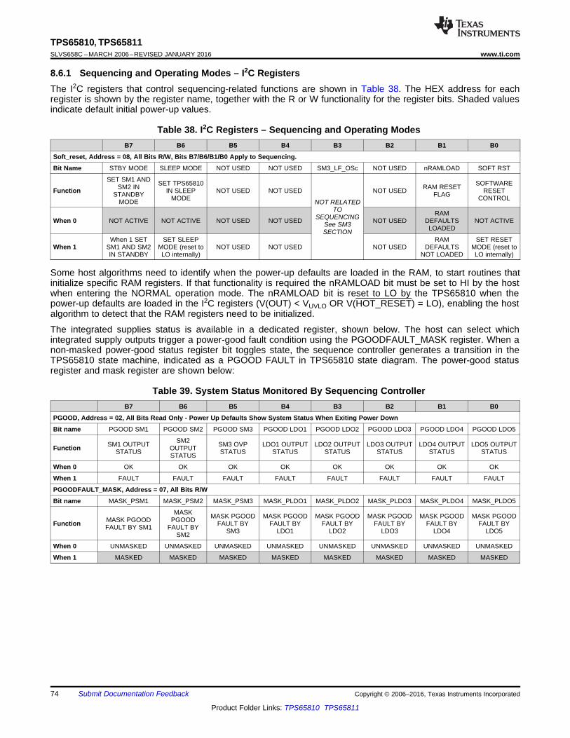
8.3.1 Interrupt Controller and System Sequencing
8.3.1.1 OverviewThe TPS65810 has two dedicated internal controllers that execute the host interface and system sequencingtasks: a sequencing controller and an interrupt controller.
The sequencing controller monitors internal and system parameters and defines the sequencing of the internalpower supplies during power-up, power-down, or power fault events, and executes specific internal power supplyreset operations under external hardware control or host software commands.
The following parameters are monitored by the sequencing controller:• System power bus voltage (at SYS_IN pin), input supply voltage, battery pack voltage• TPS65810 thermal fault status• Integrated supply status
The interrupt controller monitors multiple system status parameters and signals to the host when one of themonitored parameters toggled, as a result of a system status change. The interrupt controller inputs include allthe parameters monitored by the sequencing controller plus:• Charger status• Battery pack status• ADC status
Internal I2C registers enable masking of all the monitored parameters. Using those registers, the host can selectwhich parameters trigger an interrupt or a power-good fault. Power-good faults trigger a change in the TPS65810operating mode, as detailed in the next sections.
Figure 16 shows a simplified block diagram for the TPS65810 sections that interface to the external host.
TPS65810, TPS65811www.ti.com SLVS658C –MARCH 2006–REVISED JANUARY 2016
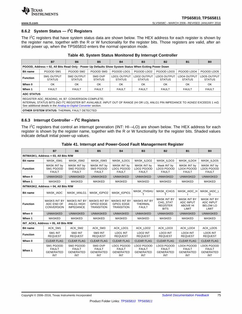
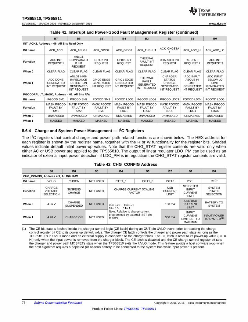
Feature Description (continued)8.3.1.2 Interrupt ControllerThe TPS65810 has internal block and overall system status information stored in I2C status registers. Thefollowing subsystems and system parameters are monitored:• External power supply status: AC or USB supply detected, AC or USB connected to system, AC/USB OVP• Charger status: on, off, or suspend, fast charge or precharge, termination detected, DPPM on, thermal loop
ON• Battery pack status: temperature, discharge on and off• TPS65810 thermal shutdown• ADC status: conversion status, input out of range, ANLG1 high impedance detection• Integrated supplies status: output out of regulation (power-good fault)
The GPIO1 and GPIO2 pins can be configured as inputs, generating an interrupt request to the host(INT:HI→LO) at the GPIO rising or falling edge. The host can use internal the INT_MASK I2C registers to definewhich of the monitored status variables triggers an interrupt. When a non-masked system status bit toggles state,the interrupt controller issues an interrupt, following the steps below:1. System status bits that caused the interruption are set to HI in registers INT_ACK1 and INT_ACK22. An interrupt is sent to the host (INT:HI→LO)
When an interrupt is sent to the host, INT is kept in the LO state and the INT_ACK register contents are latched,holding the system status that generated the currently issued interrupt request. When an interrupt request isactive (INT = LO) additional changes in non-masked status registers and control signals are ignored, and theINT_ACK registers are not updated.
The host must write a 0 to the INT_ACK register bit that generated the interrupt to set INT = HI and enable newupdates to the INT_ACK registers. If the host stops in the middle of a WRITE or READ operation, the INT pinstays at the LO level. The TPS65810 has no reset timeout; assume that the host does not leave INT = LO andthe status registers unread for a long time.
The non-masked I2C register bits and internal control signals generate a new interrupt only after INT is set to HI.The non-masked power-good fault register bits generate a power-good fault when any of the non-masked bitsdetects that the monitored output voltage is out of regulation, independently of the INT pin level.
TPS65810, TPS65811SLVS658C –MARCH 2006–REVISED JANUARY 2016 www.ti.com
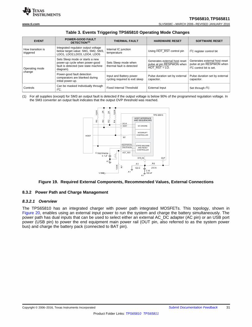
Feature Description (continued)8.3.1.3 System Sequencing and TPS65810 Operating ModesThe TPS65810 has a state machine that controls the device power-up and power-down sequencing. Figure 17 isa state diagram which shows the main operating modes.
Figure 17. TPS65810 State Diagram
8.3.1.3.1 Power Up
If the AC, USB and BAT pin voltages are below the internal UVLO threshold VUVLO (2.5 V typical) all IC blocksare disabled and the TPS65810 is not operational, with all functions OFF. When an external power source orbattery with voltage greater than the VUVLO voltage threshold is applied to AC/USB or BAT pins the internalTPS65810 references are powered up, biasing internal circuits. When all the main internal supply rails are activethe TPS65810 I2C registers are set to the power-up default values, shown in Table 1.
SUPPLY POWER-UP DEFAULT OTHER BLOCKS POWER-UP DEFAULTLDO0 OFF, 3.3 V POWER PATH INPUT TO SYSTEMLDO1 1.25V, OFF PWM OFFLDO2 3.3 V, OFF PWM_LED OFFLDO3 1.505 V, OFF GPIO1 INPUT, SM1 ON/OFF CONTROLLDO4 1.811 V, OFF GPIO2 INPUT, SM2 ON/OFF CONTROLLD05 3.111 V, ON GPIO3 INPUTSIM 2.5 V, ON ADC OFFRTC_OUT ON, 1.5 V SM3 (WHITE LED) OFFLDO_PM 3.3 V, ON at OUT POWERED RGB DRIVER OFFSM1 OFF, 1.24 V INTERRUPT MASK NONE MASKEDSM2 OFF, 3.32 V POWER-GOOD MASK ALL MASKEDCHARGER OFF
After the internal I2C register power-up defaults are loaded the power path control logic is enabled, connectingthe external power source to the OUT pin. A status flag (nRAMLOAD) is set to LO in the SOFT_RESET register,indicating that the I2C registers were loaded with the power-up defaults, and the TPS65810 enters the ENABLEstate.
8.3.1.3.2 Enable
In the ENABLE mode the RESPWRON output is set to the LO level, the INT pin mode is set to high impedanceand all the power-good comparators that monitor the integrated supply outputs are disabled. The ENABLE modeis used by the TPS65810 to detect when the main system power rail (OUT pin) is powered and ready to be usedon the internal supply power-up. The OUT pin voltage is sensed by an internal low-system-voltage comparatorwhich holds the IC in the ENABLE mode until the system power-bus voltage (OUT pin) has reached a minimumoperating voltage, defined by the user. The internal comparator senses the system voltage at pin SYS_IN, andthe threshold for the minimum system operating voltage at the OUT pin is set by the external divider connectedfrom OUT pin to SYS_IN pin. The threshold voltage is calculated in Equation 1.
where• R6 and R1 are external resistors• V(LOW_SYS) = 1 V (typical) (1)
The minimum system operating voltage must always be set above the internal UVLO threshold VUVLO. In normalapplication conditions the minimum system operating voltage is usually set to a value that assures that theTPS65810 integrated regulators are not operating in the dropout region.
When the voltage at the SYS_IN pin exceeds the internal threshold V(LOW_SYS) the TPS65810 device is ready tostart the system power sequencing, and the SEQUENCING mode is entered.
8.3.1.3.3 Sequencing
The sequencing state starts immediately after the enable state. In this mode of operation the integrated suppliesare turned ON. The TPS65810 sequencing timing diagram shown in Figure 18 details the internal timing delaysand supply sequencing. At the end of the sequencing state the user-programmable reset timer is started, and theTPS65810 enters the reset state.
TPS65810, TPS65811SLVS658C –MARCH 2006–REVISED JANUARY 2016 www.ti.com
(1) SM1 and SM2 are externally enabled by GPIO1 and GPIO2. This waveform represents the earliest time that SM1 andSM2 are enabled if GPIO1 and GPIO2 are tied high.
(2) LDO5, SM1, and SM2 are all enabled at the same time. This waveform represents the earliest time that LDO5 isenabled if VIN_LDO35 is connected to OUT. LDO5 power up can be synchronized to SM1 or SM2 by connectingVIN_LDO35 to the SM1 or SM2 output, respectively.
Figure 18. TPS65810 Supply Sequencing Timing
8.3.1.3.4 Reset
When the reset state starts the RESPWRON output is LO. The user can program the reset timer value byselecting the value of the external capacitor connected to pin TRSTPWON, as shown in Equation 2.
T(RESET) = KRESET °CTRSTPWON
where• KRESET is the reset timer constant (1 ms/nF typical) (2)
TPS65810, TPS65811www.ti.com SLVS658C –MARCH 2006–REVISED JANUARY 2016
The TPS65810 RESPWRON pin must be used to reset the external host. During the external host reset(RESPWRON = LO) the I2C SDA and SCL pins are not used to access TPS65810 internal registers. If a non-standard configuration is used to reset the system the SDA and SCL lines must not be used to communicate withthe TPS65810 until RESPWRON = HI, to avoid overwriting the integrated power supply internal power-upsettings during the sequencing mode.
The power-good comparators are masked during the reset mode. The reset mode ends when the reset timerexpires, and the TPS65810 goes into the power-good check mode.
The RESPWRON signal set to a high level is the proper signal to use as an indicator that the device hastransitioned out of the reset state. During the power-up sequence the RESPWRON pin is asserted LOW until theRESET TIMER expires. The RESET TIME (treset = 1ms/nF × CTRSTPWON) can be programmed through acapacitor between the TRSTPWON pin and ground.
When the RESPWRON signal is LO, all internal and external interrupts are ignored. As a result, the open-drainoutput that asserts the INT pin LO during a NORMAL MODE interrupt request is disabled. The INT pin is thenasserted HI through a pullup resistor that is typically connected to VOUT. After the RESPWRON signal goes HI,the interrupt controller is given control of the INT pin. Finally, the rising edge of the RESPWRON pin must beused to indicate the PMIC has transitioned from the RESET STATE to the POWER-GOOD CHECK STATE. Atthat point, the interrupt controller asserts an interrupt if necessary.
8.3.1.3.5 Power-Good Check
In the power-good check mode the power-good comparators are enabled, providing status on the integratedsupplies output voltages. An output voltage is considered as out of regulation and generates a fault condition ifthe output voltage is below 90% of the target output voltage regulation value. If a power-good fault is detectedthe SLEEP mode is set, if a power-good fault is not detected the NORMAL mode is set.
The individual supply power-good status can be masked through an I2C register PGOODFAULT_MASK.Supplies that have their power-good fault status masked do not generate a power-good fault. However, thestatus bit for the supply indicates that the output voltage is out of regulation.
The power-good mask register bits default to masked upon power up.
8.3.1.3.6 Sleep Mode
The SLEEP mode is set when a thermal fault or system low voltage fault is detected, under NORMAL operationmode set. This operation mode is also set when a power-good fault is detected during the power-good checkstate or the I2C bit SLEEP_MODE. In the SLEEP mode the RESPWRON output is set to LO, and the I2Cregisters keep the same contents as in the state preceding SLEEP mode, with the exception of the followingcontrol bits, which are reset to the default power-up values:1. LDO1,2,3,4,5 and RTC_OUT are enabled, SIM LDO is disabled: EN_LDO register set to default values2. LDO0 disabled, all GPIOs with no control function assigned: GPIO12, GPIO3 registers set to default values3. White LED driver is set to OFF: SM3_SET register has all bits set to LO4. RGB drivers are set to OFF: RGB_FLASH, RGB_RED, RGB_GREEN, RGB_BLUE registers are set to
default values5. PWM, PWM_LED drivers OFF: PWM, LED_PWM registers are set to default values6. ADC engine reset to power-up default: ADC_SET, ADC_DELAY, ADC_WAIT registers are set to default
values
NOTEIn SLEEP mode the power path and main internal blocks are still active, but the internalintegrated supply sequencing is disabled. As a result of that, during SLEEP mode ALLintegrated supplies (ALL LDO's, ALL buck Converters) are disabled.
At the end of the SLEEP mode, the sequencer block uses the I2C control register values (which were reset to thedefault power-up values) to sequence the integrated power supplies. The SLEEP mode ends when one of thethree following events occurs:1. If SLEEP was set by thermal fault: The SLEEP mode ends only when all external input supplies and battery
pack are removed and a UVLO condition is detected by the TPS65810, setting the NO POWER mode.
TPS65810, TPS65811SLVS658C –MARCH 2006–REVISED JANUARY 2016 www.ti.com
2. If SLEEP was set by a system low voltage detection, or I2C bit SLEEP_MODE, only with battery present:Input power must be connected, setting the TPS65810 in the ENABLE mode. If no input power is inserted,the battery discharges until the TPS65810 detects a UVLO condition and enters the NO POWER mode.
3. If sleep was set by a system low voltage detection, power-good fault or SLEEP_MODE, with battery andinput power present: all external input supplies connected to AC and USB pins must be removed, and then atleast one of them reconnected to the system. The input power cycling triggers a transition from SLEEP modeto the ENABLE mode.
8.3.1.3.7 Normal Mode
If a power-good fault is not present at the end of the power-good check mode the NORMAL mode starts. In thismode of operation the I2C registers define the TPS65810 operation, and the host has full control on operationmodes, parameter settings, and so forth. The normal state operation ends if a thermal fault, system low voltagefault (V(SYS_IN) < VLOW_SYS) or power-good fault is detected. A thermal fault or system low voltage fault sets theSLEEP mode operation, a power-good fault sets the NO POWER operation mode. From the normal mode theconverters SM1 and SM2 can be set in the STANDBY mode, with reduced output voltages. In NORMAL modeeither an I2C register bit (SOFT_RESET register bit SOFT_RST) or a hardware input ( HOT_RESET pin set toLO) can trigger a transition to the RESET state, enabling implementation of a host reset function. In NORMALmode an I2C register bit (SOFT_RESET register bit SLEEP_MODE) can trigger a transition to SLEEP mode.
8.3.1.3.8 Processor Standby State
This state is set using an I2C register or a GPIO configured as SM1 and SM2 stand-by control. In stand-by modeoperation, the SM1 and SM2 voltages are set to value distinct than the normal mode output voltage, andSM1/SM2 are set to PFM mode. The stand-by output voltage is defined in I2C registers SM1_STANDBY andSM2_STANDBY.
8.3.1.4 TPS65810 Operating Mode ControlsThe three operating mode controls are defined as follows:
HARDWARE RESET A dedicated control pin, HOT_RESET, enables implementation of a hardware resetfunction. The system reset pin RESPWRON is set to LO when HOT_RESET = LO for a periodlonger than the internal deglitch (5 ms typical). The RESET mode is started when the HOT_RESETpin transitions from LO to HI, as shown in the state diagram. When HOT_RESET = LO all I2Cregisters are reset to the default power-up values.
SOFTWARE RESET The external host can set the TPS65810 device in RESET mode using the I2C registerSOFT_RESET, bit B0 (SOFT_RST).
SOFTWARE SLEEP The external host can set the TPS65810 in SLEEP mode using the I2C registerSOFT_RESET, bit B6 (SLEEP_MODE).
A software reset does not affect the contents of the I2C registers.
8.3.1.5 Functionality Reference Guide – Host Interface and System Sequencing
Table 2. Interrupt Controller, Open-Drain Output (INT)SYSTEM PARAMETERS MONITORED BY THE INTERRUPT CONTROLLER
POWER UPSUPPLY OUTPUT SYSTEM STATUS CHARGER STATUS INPUT AND OUTPUT DEFAULTPOWER-GOOD FAULT ADC STATUSMODIFICATION TRANSITION POWER TRANSITIONDETECTION(1)
SM1,SM2, Thermal Fault or GPIO ADC conversion end ADC Charge: Pre↔ Fast ↔Done AC detected: yes ↔ noSM3, 1,2 configured as Input out of range DPPM:on ↔ off USB detected: yes ↔ no
All interruptLDO1, LDO2, external interrupt External resistive load Charge Suspend: on ↔ off Input OVP: yes ↔ nocontroller inputs setLDO3, LDO4, request connected to ANLG1 Thermal Foldback: on ↔ off System Power: AC ↔ USB
to non-maskedLDO5
Can be masked Individually throughCan be masked Individually through I2C Can be masked as a group through a single I2C mask register bitI2C. Blanked during initial power up
(1) For all supplies (except) for SM3 an output fault is detected if the output voltage is below 90% of the programmed regulation voltage. Inthe SM3 converter an output fault indicates that the output OVP threshold was reached.
Integrated regulator output voltageHow transition is Internal IC junctionbelow target value: SM1, SM2, SM3, Using HOT_RST control pin I2C register control bittriggered temperatureLDO1, LDO2,LDO3, LDO4, LDO5
Sets Sleep mode or starts a new Generates external host resetGenerates external host resetpower-up cycle when power-good Sets Sleep mode when pulse at pin RESPWON whenpulse at pin RESPWON whenfault is detected (see state machine thermal fault is detected HOT_RST = LO. I2C control bit is set.Operating mode diagram).change
Power-good fault detection Input and Battery power Pulse duration set by external Pulse duration set by externalcomparators are blanked during cycling required to exit sleep capacitor. capacitor.initial power-up.
Can be masked Individually throughControls Fixed Internal Threshold External Input Set through I2CI2C.
(1) For all supplies (except) for SM3 an output fault is detected if the output voltage is below 90% of the programmed regulation voltage. Inthe SM3 converter an output fault indicates that the output OVP threshold was reached.
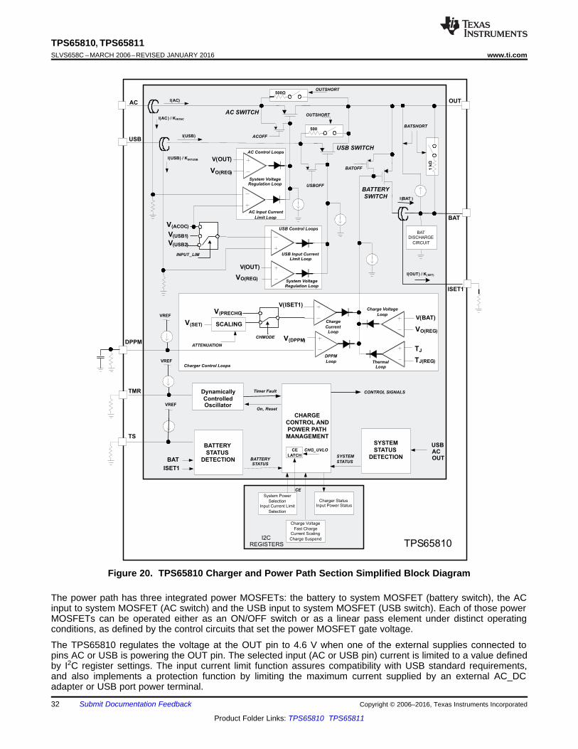
8.3.2.1 OverviewThe TPS65810 has an integrated charger with power path integrated MOSFETs. This topology, shown inFigure 20, enables using an external input power to run the system and charge the battery simultaneously. Thepower path has dual inputs that can be used to select either an external AC_DC adapter (AC pin) or an USB portpower (USB pin) to power the end equipment main power rail (OUT pin, also referred to as the system powerbus) and charge the battery pack (connected to BAT pin).
TPS65810, TPS65811SLVS658C –MARCH 2006–REVISED JANUARY 2016 www.ti.com
Figure 20. TPS65810 Charger and Power Path Section Simplified Block Diagram
The power path has three integrated power MOSFETs: the battery to system MOSFET (battery switch), the ACinput to system MOSFET (AC switch) and the USB input to system MOSFET (USB switch). Each of those powerMOSFETs can be operated either as an ON/OFF switch or as a linear pass element under distinct operatingconditions, as defined by the control circuits that set the power MOSFET gate voltage.
The TPS65810 regulates the voltage at the OUT pin to 4.6 V when one of the external supplies connected topins AC or USB is powering the OUT pin. The selected input (AC or USB pin) current is limited to a value definedby I2C register settings. The input current limit function assures compatibility with USB standard requirements,and also implements a protection function by limiting the maximum current supplied by an external AC_DCadapter or USB port power terminal.
TPS65810, TPS65811www.ti.com SLVS658C –MARCH 2006–REVISED JANUARY 2016
The AC power MOSFET and USB power MOSFET operating modes are set by integrated control loops. Each ofthe power MOSFETs is controlled by two loops: one system voltage regulation loop and one input current limitingloop. The integrated loops modulate the AC or USB power MOSFETs drain to source resistance to regulateeither the OUT pin voltage or to limit the input current. If no input power is present (AC and USB input power notdetected) the AC and USB power MOSFETs are turned OFF, and the battery MOSFET is turned ON, connectingthe BAT pin to the OUT pin.
The battery switch is turned ON when the AC or USB input power is detected and the charger function isenabled, charging the battery pack. During charge the battery MOSFET switch operation mode is defined by thecharger control loops. The battery MOSFET switch drain-to-source resistance is modulated by the charge currentloop and charge voltage loop to implement the battery charging algorithm. In addition to that multiple safetyfunctions are activated (thermal shutdown, safety timers, short-circuit recovery), and additional functions (thermalloop and DPPM loop) optimize the charging process.
8.3.2.2 Power Path Management Function
8.3.2.2.1 Detecting the System Status
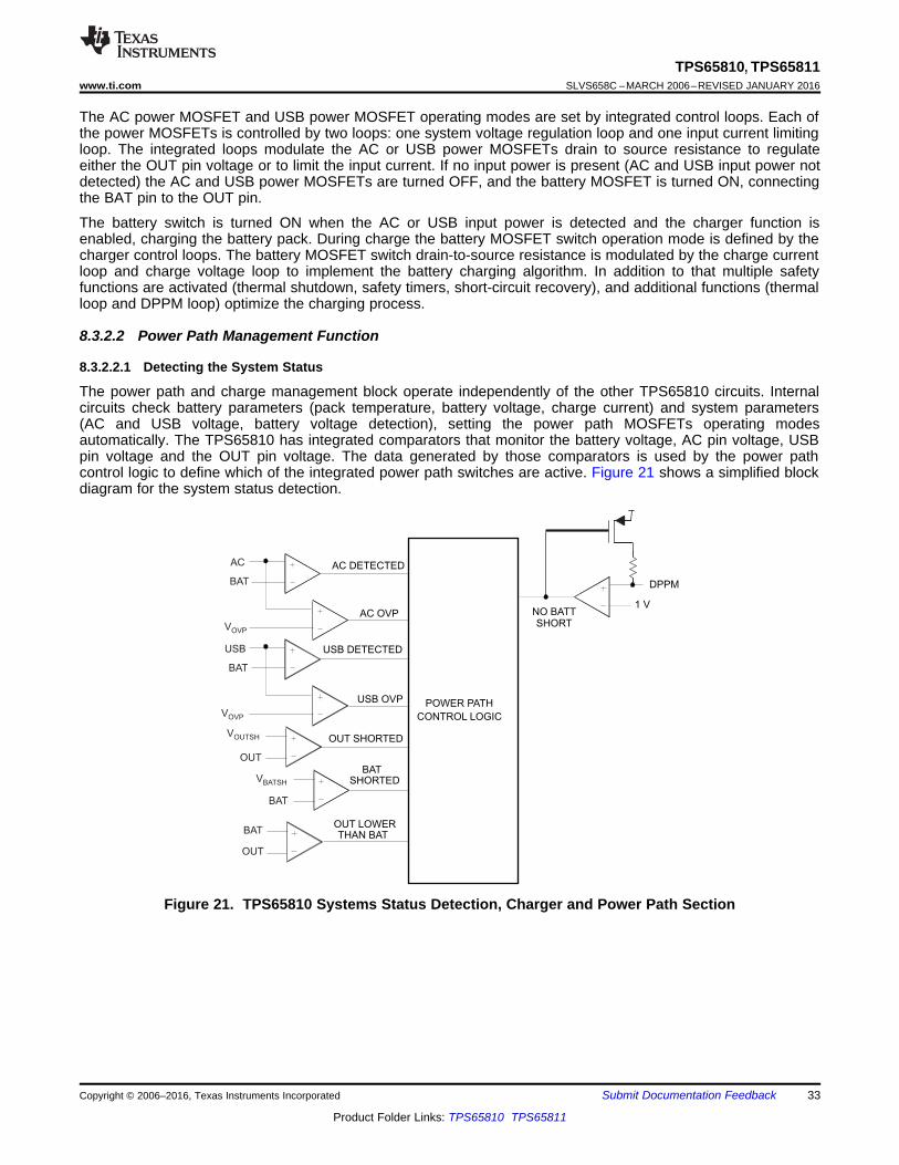
The power path and charge management block operate independently of the other TPS65810 circuits. Internalcircuits check battery parameters (pack temperature, battery voltage, charge current) and system parameters(AC and USB voltage, battery voltage detection), setting the power path MOSFETs operating modesautomatically. The TPS65810 has integrated comparators that monitor the battery voltage, AC pin voltage, USBpin voltage and the OUT pin voltage. The data generated by those comparators is used by the power pathcontrol logic to define which of the integrated power path switches are active. Figure 21 shows a simplified blockdiagram for the system status detection.
Figure 21. TPS65810 Systems Status Detection, Charger and Power Path Section
TPS65810, TPS65811SLVS658C –MARCH 2006–REVISED JANUARY 2016 www.ti.com
Table 4 lists the system power detection conditions. VIN(DT), VOUTSH, VBATSH, VOVP are the TPS65810 internalreferences, refer to the electrical characteristics in the Specifications section for additional details.
Table 4. System Status Detection, Charger and Power Path SectionSYSTEM STATUS DETECTION CONDITION
AC input voltage detected V(AC) – V(BAT) > VIN(DT)
USB input voltage detected V(USB) – V(BAT) > VIN(DT)
AC overvoltage detected V(AC) > VOVP
USB overvoltage detected V(USB) > VOVP
AC PIN TO OUT pin OR USB TO OUT PIN short detected V(OUT) < VINOUTSH
BAT pin to OUT pin short detected V(BAT) - V(OUT) > VBATOUTSH
Battery supplement mode need detected V(BAT) – V(OUT) > VSUP
Blank BAT to OUT short circuit detection V(DPPM) < 1V
8.3.2.2.2 Power Path Logic: Priority Algorithm
The system power bus supply is automatically selected by the power path control logic, following an internalalgorithm. The power path function detects an external input power connection when the input voltage exceedsthe battery pack voltage. It also detects a supplement mode need (battery switch must be turned ON) when thesystem voltage (OUT pin) is below the battery voltage. A connected and non-selected external supply or thebattery is automatically switched to the system bus, following the priority algorithm, when the external supplycurrently selected is disconnected from the system.
The input power priority is hard-wired internally, with the AC input having the higher priority, followed by the USBinput (2nd) and the battery pack (3rd). Using the I2C CHG_CONFIG register control bit CE the user can overridethe power path algorithm, connecting the battery to the system power bus. Take care when using the battery-to-system connection option, as the system power bus is not connected back to the AC or USB inputs (even ifthose are detected) when the battery is removed. Table 5 describes the priority algorithm.
Table 5. Power Path Control Logic Priority AlgorithmEXTERNAL SUPPLY SWITCH MODECE BIT SYSTEM POWERDETECTED
SOURCE(I2C CHG_CONFIG Register)AC USB AC USB BATTERY
YES NO ON OFF AC
NO YES OFF ON USBON if Supplement mode isHI required, OFF otherwiseYES YES ON OFF AC
NO NO OFF OFF BATTERY
LO XX XX OFF OFF ON BATTERY
The power path status is stored in register CHG_STAT.
8.3.2.2.3 Input Current Limit
The USB input current is limited to the maximum value programmed by the host, using the I2C interface. If thesystem current requirements exceed the input current limit, the output voltage collapses, the charge current isreduced, and finally, the supplement mode is set. The input current limit value is set with the I2C charge controlregister bits PSEL and ISET2, and it is applied to the USB input ONLY. The AC input current limit is fixed to theinternal short circuit limit value.
Table 6. Charge-Current Scaling Through I2CINPUT CURRENT LIMIT
PSEL (I2C) ISET2 (I2C)USB AC
LO LO 100 mA 2.75 ALO HI 500 mA 2.75 AHI LO 2.75 A 2.75 AHI HI 2.75 A 2.75 A
TPS65810, TPS65811www.ti.com SLVS658C –MARCH 2006–REVISED JANUARY 2016
8.3.2.2.4 System Voltage Regulation
The system voltage is regulated to a fixed voltage when one of the input power supplies is connected to thesystem. The system voltage regulation is implemented by a control loop that modulates the selected switchRds(on).
The typical system regulation voltage is 4.6 V.
8.3.2.2.5 Input Overvoltage Detection
The AC and USB input voltages are monitored by voltage comparators that identify an overvoltage condition. Ifan overvoltage condition is detected a status register bit is set, indicating a potential fault condition.
When an overvoltage condition is detected, the AC or USB switches state is not modified. If any of thoseswitches was ON, it is kept in the ON state. During overvoltage conditions, the system voltage is still regulated,and no major safety issues are observed when not modifying the input switch state.
If the input overvoltage condition results in excessive power dissipation, the thermal shutdown circuit is activated,the AC and USB switches are turned OFF, and the BAT switch is turned ON.
8.3.2.2.6 Output Short-Circuit Detection
If the OUT pin voltage falls below an internal threshold VINOUTSH the AC and USB switches are turned off andinternal pullup resistors are connected from AC pin to OUT pin and USB pin to OUT pin. When the short circuit isremoved those resistors enable the OUT pin voltage to rise above the VINOUTSH threshold, returning the system tonormal operation.
8.3.2.2.7 Battery Short-Circuit Detection
If the OUT pin voltage falls below the BAT pin voltage by more than an internal threshold VBATOUTSH the batteryswitch is turned off and internal pullup resistor is connected between the OUT pin and the BAT pin. This resistorenables detection of the short removal, returning the system to normal operation.
8.3.2.2.8 Initial Power Path Operation
During the initial TPS65810 power-up the contents of the ISET2, CE and SUSPEND bits on the control registerare immediately implemented. The charger is disabled (SUSPEND=LO) and the selected input current limit is setinternally to 500 mA max.
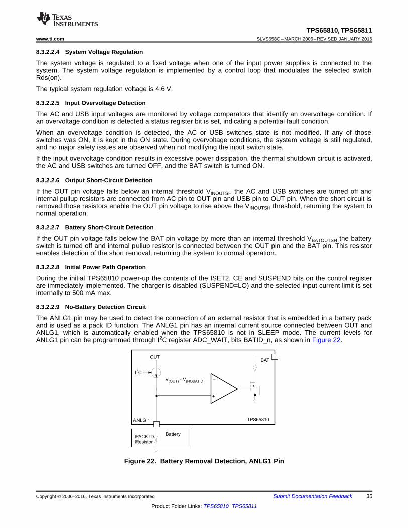
8.3.2.2.9 No-Battery Detection Circuit
The ANLG1 pin may be used to detect the connection of an external resistor that is embedded in a battery packand is used as a pack ID function. The ANLG1 pin has an internal current source connected between OUT andANLG1, which is automatically enabled when the TPS65810 is not in SLEEP mode. The current levels forANLG1 pin can be programmed through I2C register ADC_WAIT, bits BATID_n, as shown in Figure 22.
TPS65810, TPS65811SLVS658C –MARCH 2006–REVISED JANUARY 2016 www.ti.com
An internal comparator with a fixed deglitch time, t DGL(NOBAT) monitors the ANLG1 pin voltage, if V(ANLG1) >V(OUT) – VNOBATID, a battery removed condition is detected and an internal discharge switch is activated,connecting an internal resistor from BAT pin to AGND1. Note that ANLG1 can also be used as an analog inputfor the ADC converter, in this case the voltage at pin ANLG1 must never exceed the V(OUT) – VNOBATID,threshold to avoid undesired battery discharge.
8.3.2.2.10 Using the Input Power to Run the System and Charge the Battery Pack
The external supply connected to AC or USB pins must be capable of supplying the system power and thecharger current. If the external supply power is not sufficient to run the system and charge the battery pack theTPS65810 executes a two-stage algorithm that prevents a low voltage condition at the system power bus:1. The charge current is reduced, until the total (charger + system current) is at a level that can be supplied by
the external input supply. This function is implemented by a dedicated charger control loop (see DynamicPower Path Management for additional details).
2. The battery switch is turned ON if the charge current is reduced to zero and the input current is not enoughto run the system. In this mode of operation both the battery and the external input power supply the systempower ( supplement operation mode).
The supplement operation mode is automatically set by the TPS65810 when the input power is switched to theOUT pin, and the OUT pin voltage falls below the battery voltage.
8.3.2.3 Battery Charge Management Function
8.3.2.3.1 Operating Modes
The TPS65810 supports charging of single-cell Li-Ion or Li-Pol battery packs. The charge process is executed inthree phases: precharge (or preconditioning), constant current and constant voltage.
The charge parameters are selectable through I2C interface and using external components. The charge processstarts when an external input power is connected to the system, the charger is enabled by the I2C registerCHG_CONFIG bits CE = HI and CHGON = HI, and the battery voltage is below the recharge threshold, V(BAT)< V(RCH). When the charge cycle starts a safety timer is activated. The safety timer timeout value is set by anexternal resistor connected to the TMR pin.
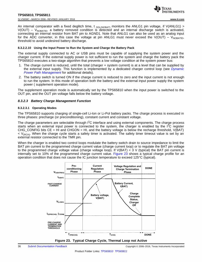
When the charger is enabled two control loops modulate the battery switch drain to source impedance to limit theBAT pin current to the programmed charge current value (charge current loop) or to regulate the BAT pin voltageto the programmed charge voltage value (charge voltage loop). If V(BAT) < 3 V (typical) the BAT pin current isinternally set to 10% of the programmed charge current value. Figure 23 shows a typical charge profile for anoperation condition that does not cause the IC junction temperature to exceed 125°C (typical).
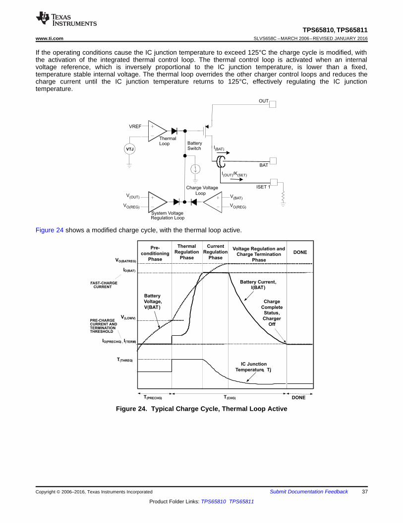
TPS65810, TPS65811www.ti.com SLVS658C –MARCH 2006–REVISED JANUARY 2016
If the operating conditions cause the IC junction temperature to exceed 125°C the charge cycle is modified, withthe activation of the integrated thermal control loop. The thermal control loop is activated when an internalvoltage reference, which is inversely proportional to the IC junction temperature, is lower than a fixed,temperature stable internal voltage. The thermal loop overrides the other charger control loops and reduces thecharge current until the IC junction temperature returns to 125°C, effectively regulating the IC junctiontemperature.
Figure 24 shows a modified charge cycle, with the thermal loop active.
Figure 24. Typical Charge Cycle, Thermal Loop Active
TPS65810, TPS65811SLVS658C –MARCH 2006–REVISED JANUARY 2016 www.ti.com
8.3.2.3.2 Battery Preconditioning
The TPS65810 applies a precharge current Io(PRECHG) to the battery if the battery voltage is below the V(LOWV)threshold, preconditioning deeply discharged cells. The charge current loop regulates the ISET1 pin voltage to aninternal reference value, V(PRECHG). The resistor connected between the ISET1 and AGND pins, RSET, determinesthe precharge rate.
The precharge rate programmed by RSET is always applied to a deeply discharged battery pack, independently ofthe input power selection (AC or USB). Use Equation 3 to calculate the precharge current.
where• K(SET) is the charge current scaling factor• V(PRECHG) is the precharge set voltage (3)
8.3.2.3.3 Constant Current Charging
The constant charge current mode (fast charge) is set when the battery voltage is higher than the prechargevoltage threshold. The charge current loop regulates the ISET1 pin voltage to an internal reference value, VSET.The fast charge current regulation point is defined by the external resistor connected to the ISET1 pin, RSET, asshown in the following:
where• V(SET) (2.5 V typical) is the voltage at ISET1 pin during charge current regulation• K(SET) = charge- current scaling factor (4)
The reference voltage V(SET) can be reduced through I2C register CHG_CONFIG bits ISET1_1 and ISET1_0.V(SET) can be selected as a percentage (75%, 50% or 25%) of the original 2.5 V typ, non-attenuated V(SET) value,effectively scaling down the charge current.
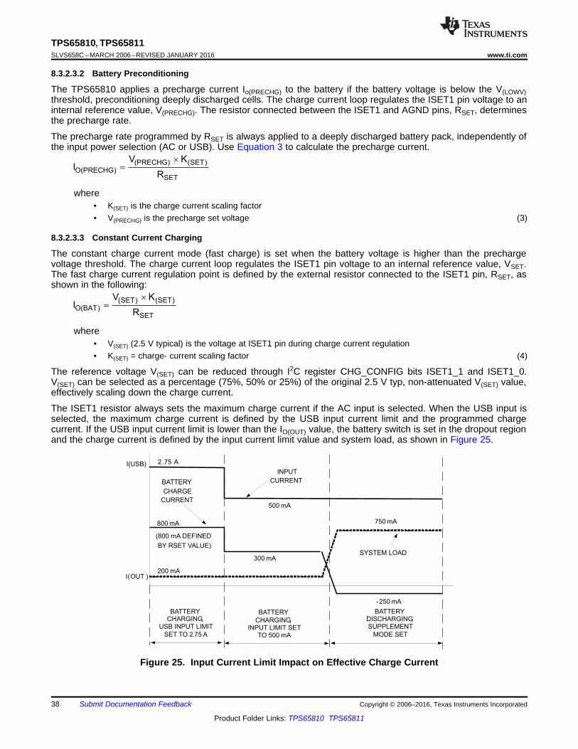
The ISET1 resistor always sets the maximum charge current if the AC input is selected. When the USB input isselected, the maximum charge current is defined by the USB input current limit and the programmed chargecurrent. If the USB input current limit is lower than the IO(OUT) value, the battery switch is set in the dropout regionand the charge current is defined by the input current limit value and system load, as shown in Figure 25.
Figure 25. Input Current Limit Impact on Effective Charge Current
TPS65810, TPS65811www.ti.com SLVS658C –MARCH 2006–REVISED JANUARY 2016
8.3.2.3.4 Charge Termination and Recharge
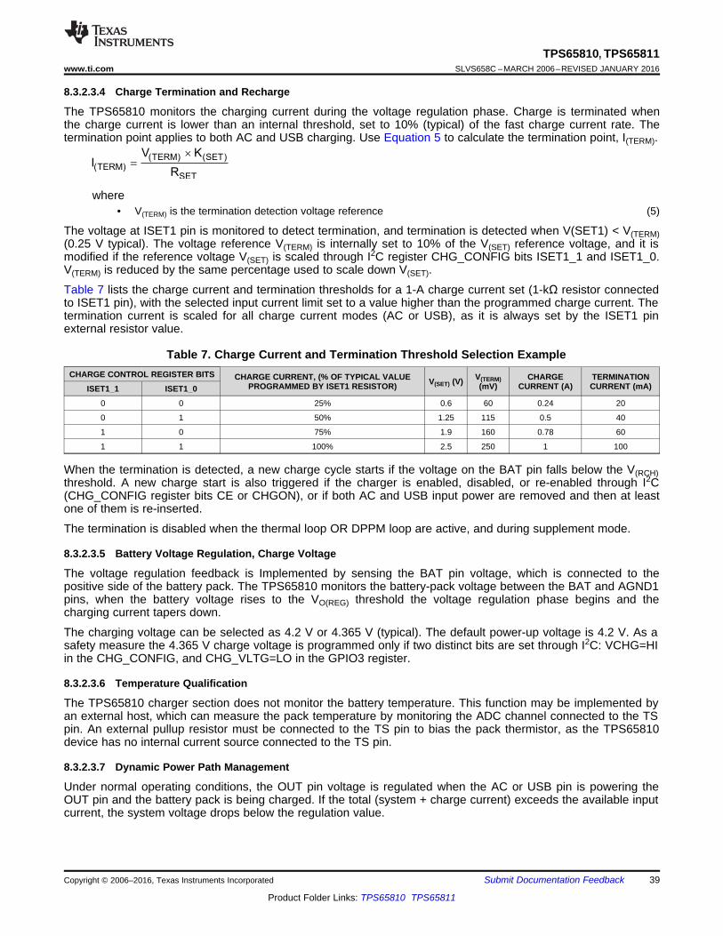
The TPS65810 monitors the charging current during the voltage regulation phase. Charge is terminated whenthe charge current is lower than an internal threshold, set to 10% (typical) of the fast charge current rate. Thetermination point applies to both AC and USB charging. Use Equation 5 to calculate the termination point, I(TERM).
where• V(TERM) is the termination detection voltage reference (5)
The voltage at ISET1 pin is monitored to detect termination, and termination is detected when V(SET1) < V(TERM)(0.25 V typical). The voltage reference V(TERM) is internally set to 10% of the V(SET) reference voltage, and it ismodified if the reference voltage V(SET) is scaled through I2C register CHG_CONFIG bits ISET1_1 and ISET1_0.V(TERM) is reduced by the same percentage used to scale down V(SET).
Table 7 lists the charge current and termination thresholds for a 1-A charge current set (1-kΩ resistor connectedto ISET1 pin), with the selected input current limit set to a value higher than the programmed charge current. Thetermination current is scaled for all charge current modes (AC or USB), as it is always set by the ISET1 pinexternal resistor value.
Table 7. Charge Current and Termination Threshold Selection ExampleCHARGE CONTROL REGISTER BITS CHARGE CURRENT, (% OF TYPICAL VALUE V(TERM) CHARGE TERMINATIONV(SET) (V)PROGRAMMED BY ISET1 RESISTOR) (mV) CURRENT (A) CURRENT (mA)ISET1_1 ISET1_0
0 0 25% 0.6 60 0.24 20
0 1 50% 1.25 115 0.5 40
1 0 75% 1.9 160 0.78 60
1 1 100% 2.5 250 1 100
When the termination is detected, a new charge cycle starts if the voltage on the BAT pin falls below the V(RCH)threshold. A new charge start is also triggered if the charger is enabled, disabled, or re-enabled through I2C(CHG_CONFIG register bits CE or CHGON), or if both AC and USB input power are removed and then at leastone of them is re-inserted.
The termination is disabled when the thermal loop OR DPPM loop are active, and during supplement mode.
8.3.2.3.5 Battery Voltage Regulation, Charge Voltage
The voltage regulation feedback is Implemented by sensing the BAT pin voltage, which is connected to thepositive side of the battery pack. The TPS65810 monitors the battery-pack voltage between the BAT and AGND1pins, when the battery voltage rises to the VO(REG) threshold the voltage regulation phase begins and thecharging current tapers down.
The charging voltage can be selected as 4.2 V or 4.365 V (typical). The default power-up voltage is 4.2 V. As asafety measure the 4.365 V charge voltage is programmed only if two distinct bits are set through I2C: VCHG=HIin the CHG_CONFIG, and CHG_VLTG=LO in the GPIO3 register.
8.3.2.3.6 Temperature Qualification
The TPS65810 charger section does not monitor the battery temperature. This function may be implemented byan external host, which can measure the pack temperature by monitoring the ADC channel connected to the TSpin. An external pullup resistor must be connected to the TS pin to bias the pack thermistor, as the TPS65810device has no internal current source connected to the TS pin.
8.3.2.3.7 Dynamic Power Path Management
Under normal operating conditions, the OUT pin voltage is regulated when the AC or USB pin is powering theOUT pin and the battery pack is being charged. If the total (system + charge current) exceeds the available inputcurrent, the system voltage drops below the regulation value.
TPS65810, TPS65811SLVS658C –MARCH 2006–REVISED JANUARY 2016 www.ti.com
The dynamic power path management function monitors the system output voltage. A condition where theexternal input supply rating has been exceeded or the input current limit has been reached is detected when theOUT pin voltage drops below an user-defined threshold, VDPPM. Use Equation 6 to calculate the value of VDPPM.
To correct this situation the DPPM loop reduces the charge current, regulating the OUT pin voltage to the user-defined VDPPM threshold. The DPPM loop effectively identifies the maximum current that can be delivered by theselected input and dynamically adjusts the charge current to guarantee that the end equipment is alwayspowered. To minimize OUT voltage ripple during DPPM operation the VDPPM threshold must be set just below thesystem regulation voltage.
If the charge current is reduced to zero by the DPPM and the input current is still lower than the OUT pin load,the output voltage falls below the DPPM threshold, decreasing until the battery supplement mode is set[V(OUT) = V(BAT) – VSUP(DT) ].
8.3.2.3.8 Charger Off Mode
The TPS65810 charger circuitry enters the low-power OFF mode if both AC and USB power are not detected.This feature prevents draining the battery during the absence of input supply.
8.3.2.3.9 Precharge Safety Timer
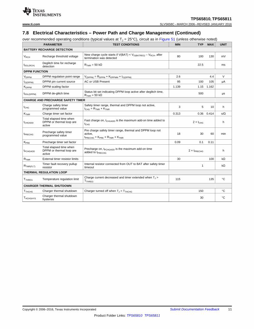
The TPS65810 device activates an internal safety timer during the battery preconditioning phase. The prechargesafety timer time-out value is set by the external resistor connected to TMR pin, RTMR, and the timeoutconstants KPRE and KTMR. Use Equation 7 to calculate the timeout value value of the precharge safety timer.
TPRECHG = KPRE × RTMR × KTMR (7)
The KPRE constant typical value is 0.1, setting the precharge timer value to 10% of the charge safety timer value.
When the charger is in suspend mode, set through I2C register CHG_CONFIG bit CHGON or set by a packtemperature fault, the precharge safety timer is put on hold (that is, charge safety timer is not reset). Normaloperation resumes when the charger exits the suspend mode. If V(BAT) does not reach the internal voltagethreshold VPRECHG within the precharge timer period a fault condition is detected and the charger is turned off.
If the TMR pin is left floating, an internal resistor of 50 KΩ (typical) is used to generate the time base used to setthe precharge timeout value. The typical precharge timeout value can be then calculated using Equation 8.
TPRECHG = KPRE × 50K × KTMR (8)
8.3.2.3.10 Charge Safety Timer
As a safety mechanism the TPS65810 has a user-programmable timer that measures the total fast charge time.This timer (charge safety timer) is started at the end of the preconditioning period. The safety charge timeoutvalue is set by the value of an external resistor connected to the TMR pin RTMR). Use Equation 9 to calculate thecharge safety timer time-out value.
TCHG = KTMR × RTMR (9)
When the charger is in suspend mode, set through I2C register CHG_CONFIG bit CHGON or set by a packtemperature fault, the charge safety timer is put on hold (that is, charge safety timer is not reset). Normaloperation resumes when the charger exits the suspend mode. If charge termination is not reached within thetimer period a fault condition is detected, and the charger is turned off.
The charge safety timer is held in reset if the TMR pin is left floating. Under this mode of operation an internalresistor, 50 kΩ typical, sets the internal charger and power path deglitch and delay times, as well as theprecharge safety timer timeout value.
TPS65810, TPS65811www.ti.com SLVS658C –MARCH 2006–REVISED JANUARY 2016
8.3.2.3.11 Timer Fault Recovery
The TPS65810 provides a recovery method to deal with timer fault conditions. The following summarizes thismethod:• Condition 1: Charge voltage above recharge threshold, V(RCH), and timeout fault occurs.
Recovery method The IC waits for the battery voltage to fall below the recharge threshold. This could happenas a result of a load on the battery, self-discharge or battery removal. When the battery falls belowthe recharge threshold, the IC clears the fault and starts a new charge cycle.
• Condition 2: Charge voltage below recharge threshold,V(RCH), and timeout fault occurs.
Recovery method Under this scenario, the IC connects an internal pullup resistor from OUT pin to BAT pin.This pullup resistor is used to detect a battery removal condition and remains on as long as thebattery voltage stays below the recharge threshold. If the battery voltage goes above the rechargethreshold, the IC disables the pullup resistor connection and executes the recovery methoddescribed for condition 1.
All timers are reset and all timer fault conditions are cleared when a new charge cycle is started either throughI2C (toggling CHG_CONFIG bits CE, CHGON) or by cycling the input power. All timers are reset and all timerfault conditions are cleared when the TPS65810 enters the UVLO mode.
8.3.2.3.12 Dynamic Timer Function
The charge and precharge safety timers are programmed by the user to detect a fault condition if the chargecycle duration exceeds the total time expected under normal conditions. The expected total charge time isusually calculated based on the fast charge current rate.
When the thermal loop or the DPPM loops are activated the charge current is reduced, and a false safety timerfault can be observed if this mode of operation is active for a long periods. To avoid this undesirable faultcondition the TPS65810 activates the dynamic timer function when the DPPM and thermal loops are active. Thedynamic timer function slows down the safety timers clock, effectively adding an extra time to the programmedtimeout value as follows:1. If the battery voltage is below the battery depleted threshold: the precharge timer value is modified while the
thermal loop or the DPPM loop are active2. If the battery voltage is above the precharge threshold: the safety timer value is modified if the DPPM or the
thermal loop are active AND the battery voltage is below the recharge threshold.
The TPS65810 dynamic timer function circuit monitors the voltage at pin ISET1 during precharge and fastcharge. When the charger is regulating the charge current, the voltage at pin ISET1 is regulated by the controlloops to either V(SET) or V(PRECHG). If the thermal loop or DPPM loops are active, the voltage at pin ISET1 is lowerthan V(SET) or VPRECHG, and the dynamic timer control circuit changes the safety timers clock period based on theV(SET)/V(ISET1) ratio (fast charge) or V(PRECHG)/V(ISET1) ratio (precharge).
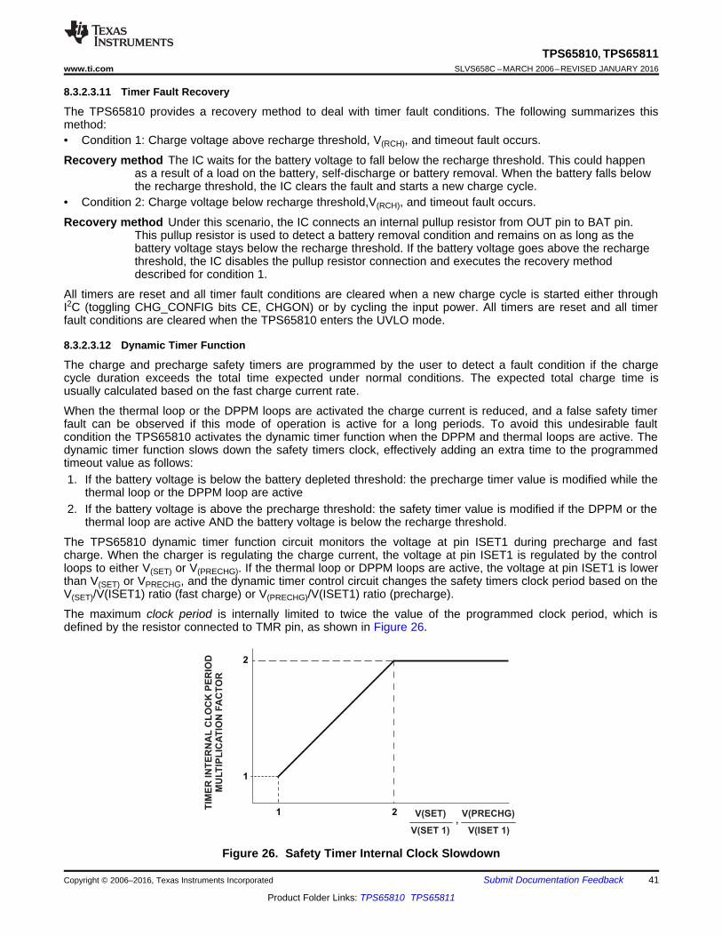
The maximum clock period is internally limited to twice the value of the programmed clock period, which isdefined by the resistor connected to TMR pin, as shown in Figure 26.
Fast Charge Current = 1A (100% scaling, input limit=2.5A)Safety Timer = 5hours, 30 min pre-charge
DPPM threshold = 4.3VTemp hot: 65C
Temp Cold : 5C
System Power
SelectionInput Current Limit
Selection
Charge VoltageFast Charge
Current ScalingCharge Suspend
I2C REGISTERS
R
37.4 kDPPM
W
A1
C26
22 Fm
C25
10 Fm50 k
NTCW
R
49.9 kTMR
W
C2
10 Fm
C2347 nF
A1
R
1 kSET
W
A1
C24
0.22 Fm
A1
C1
10 Fm
TPS65810, TPS65811SLVS658C –MARCH 2006–REVISED JANUARY 2016 www.ti.com
The effective charge safety timer value can then be expressed as follows:Effective precharge timeout = t(PRECHG) + t(PCHGADD)Effective charge safety timeout = t(CHG) + t(CHGADD)
The added timeout values, t(PCHGADD), t(CHGADD), are equal to the sum of all time periods when either the thermalloop or DPPM loops were active. The maximum added timeout value is internally limited to 2 × t(CHG) or 2 ×t(PRECHG)
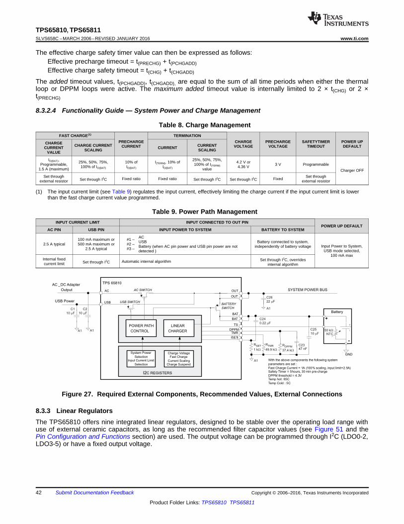
8.3.2.4 Functionality Guide — System Power and Charge Management
PRECHARGE CHARGE PRECHARGE SAFETYTIMER POWER UPCHARGE CHARGE CURRENT CURRENTCURRENT VOLTAGE VOLTAGE TIMEOUT DEFAULTCURRENT CURRENTSCALING SCALINGVALUE
IO(BAT), 25%, 50%, 75%,25%, 50%, 75%, 10% of I(TERM), 10% of 4.2 V orProgrammable, 100% of I(TERM) 3 V Programmable100% of IO(BAT) IO(BAT) IO(BAT) 4.36 V1.5 A (maximum) value Charger OFFSet through Set throughFixed ratio Fixed ratio FixedSet through I2C Set through I2C Set through I2Cexternal resistor external resistor
(1) The input current limit (see Table 9) regulates the input current, effectively limiting the charge current if the input current limit is lowerthan the fast charge current value programmed.
Table 9. Power Path ManagementINPUT CURRENT LIMIT INPUT CONNECTED TO OUT PIN
POWER UP DEFAULTAC PIN USB PIN INPUT POWER TO SYSTEM BATTERY TO SYSTEM
AC100 mA maximum or #1 – USB Battery connected to system,2.5 A typical 500 mA maximum or #2 – Input Power to System,Battery (when AC pin power and USB pin power are not independently of battery voltage2.5 A typical #3 – USB mode selected,detected )100 mA max
Internal fixed Set through I2C, overridesAutomatic internal algorithmSet through I2Ccurrent limit internal algorithm
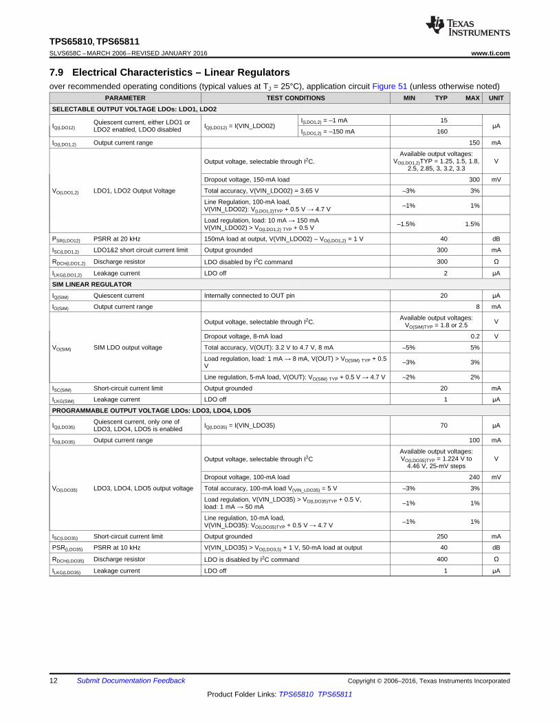
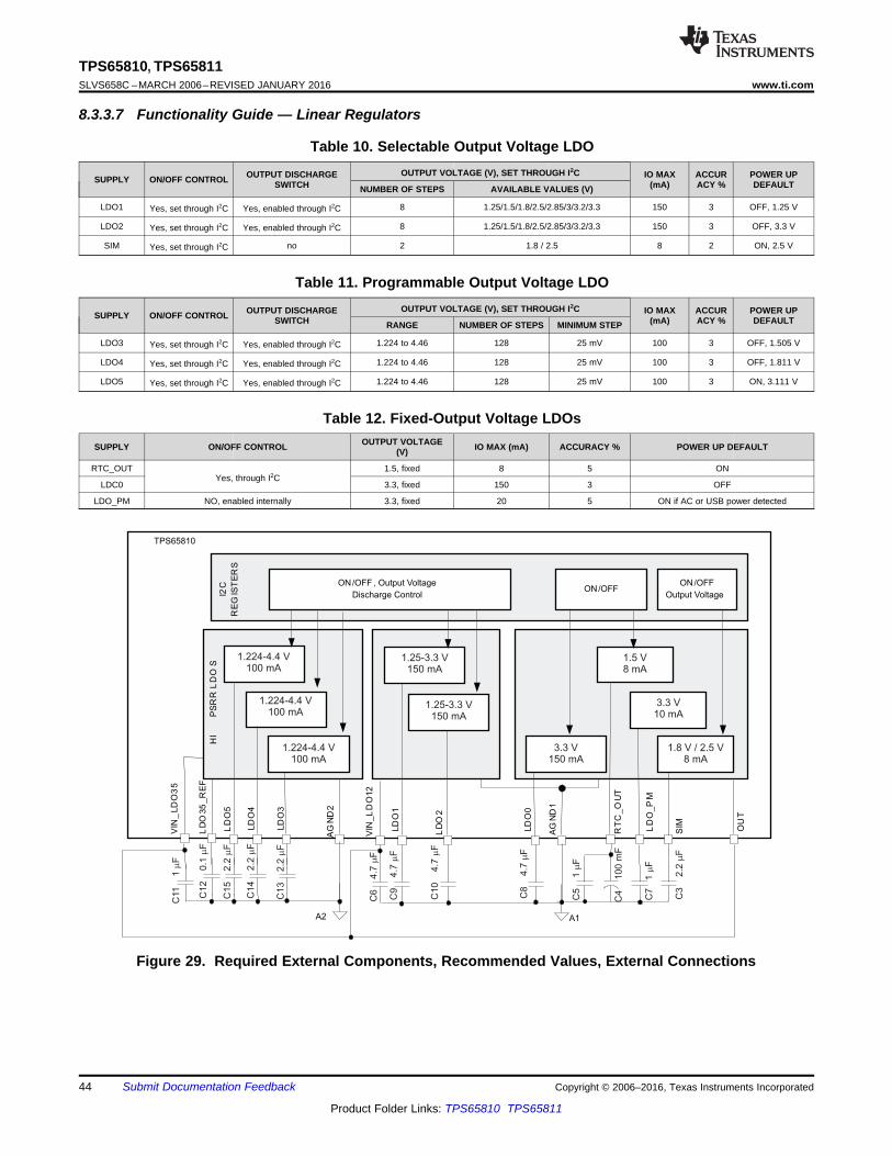
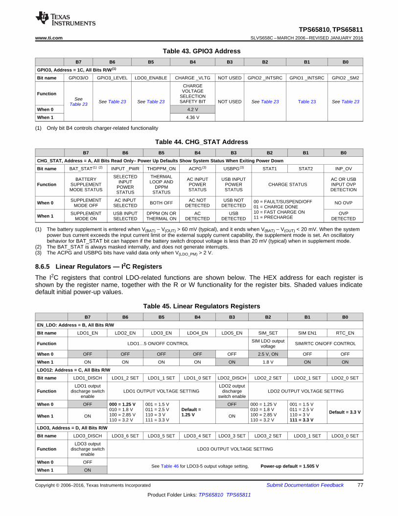
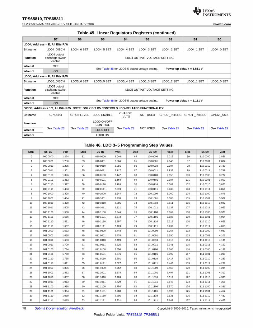
8.3.3 Linear RegulatorsThe TPS65810 offers nine integrated linear regulators, designed to be stable over the operating load range withuse of external ceramic capacitors, as long as the recommended filter capacitor values (see Figure 51 and thePin Configuration and Functions section) are used. The output voltage can be programmed through I2C (LDO0-2,LDO3-5) or have a fixed output voltage.
TPS65810, TPS65811www.ti.com SLVS658C –MARCH 2006–REVISED JANUARY 2016
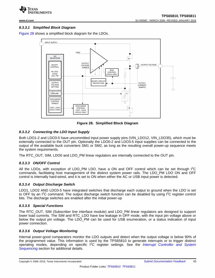
8.3.3.1 Simplified Block DiagramFigure 28 shows a simplified block diagram for the LDOs.
Figure 28. Simplified Block Diagram
8.3.3.2 Connecting the LDO Input SupplyBoth LDO1-2 and LDO3-5 have uncommitted input power supply pins (VIN_LDO12, VIN_LDO35), which must beexternally connected to the OUT pin. Optionally the LDO0-2 and LDO3-5 input supplies can be connected to theoutput of the available buck converters SM1 or SM2, as long as the resulting overall power-up sequence meetsthe system requirements.
The RTC_OUT, SIM, LDO0 and LDO_PM linear regulators are internally connected to the OUT pin.
8.3.3.3 ON/OFF ControlAll the LDOs, with exception of LDO_PM LDO, have a ON and OFF control which can be set through I2Ccommands, facilitating host management of the distinct system power rails. The LDO_PM LDO ON and OFFcontrol is internally hard-wired, and it is set to ON when either the AC or USB input power is detected.
8.3.3.4 Output Discharge SwitchLDO1, LDO2 AND LDO3-5 have integrated switches that discharge each output to ground when the LDO is setto OFF by an I2C command. The output discharge switch function can be disabled by using I2C register controlbits. The discharge switches are enabled after the initial power-up
8.3.3.5 Special FunctionsThe RTC_OUT, SIM (Subscriber line interface module) and LDO_PM linear regulators are designed to supportlower load currents. The SIM and RTC_LDO have low leakage in OFF mode, with the input pin voltage above orbelow the output pin voltage. The LDO_PM can be used for USB enumeration, or a status indication of inputpower connection.
8.3.3.6 Output Voltage MonitoringInternal power-good comparators monitor the LDO outputs and detect when the output voltage is below 90% ofthe programmed value. This information is used by the TPS65810 to generate interrupts or to trigger distinctoperating modes, depending on specific I2C register settings. See the Interrupt Controller and SystemSequencing section for additional details.
TPS65810, TPS65811SLVS658C –MARCH 2006–REVISED JANUARY 2016 www.ti.com
8.3.3.7 Functionality Guide — Linear Regulators
Table 10. Selectable Output Voltage LDOOUTPUT VOLTAGE (V), SET THROUGH I2COUTPUT DISCHARGE IO MAX ACCUR POWER UPSUPPLY ON/OFF CONTROL SWITCH (mA) ACY % DEFAULTNUMBER OF STEPS AVAILABLE VALUES (V)
LDO1 8 1.25/1.5/1.8/2.5/2.85/3/3.2/3.3 150 3 OFF, 1.25 VYes, set through I2C Yes, enabled through I2C
LDO2 8 1.25/1.5/1.8/2.5/2.85/3/3.2/3.3 150 3 OFF, 3.3 VYes, set through I2C Yes, enabled through I2C
SIM no 2 1.8 / 2.5 8 2 ON, 2.5 VYes, set through I2C
Table 11. Programmable Output Voltage LDOOUTPUT VOLTAGE (V), SET THROUGH I2COUTPUT DISCHARGE IO MAX ACCUR POWER UPSUPPLY ON/OFF CONTROL SWITCH (mA) ACY % DEFAULTRANGE NUMBER OF STEPS MINIMUM STEP
LDO3 1.224 to 4.46 128 25 mV 100 3 OFF, 1.505 VYes, set through I2C Yes, enabled through I2C
LDO4 1.224 to 4.46 128 25 mV 100 3 OFF, 1.811 VYes, set through I2C Yes, enabled through I2C
LDO5 1.224 to 4.46 128 25 mV 100 3 ON, 3.111 VYes, set through I2C Yes, enabled through I2C
Table 12. Fixed-Output Voltage LDOsOUTPUT VOLTAGESUPPLY ON/OFF CONTROL IO MAX (mA) ACCURACY % POWER UP DEFAULT(V)
RTC_OUT 1.5, fixed 8 5 ONYes, through I2C
LDC0 3.3, fixed 150 3 OFF
LDO_PM NO, enabled internally 3.3, fixed 20 5 ON if AC or USB power detected
TPS65810, TPS65811www.ti.com SLVS658C –MARCH 2006–REVISED JANUARY 2016
8.3.4 Step-Down Switched-Mode Converters: SM1 and SM2The TPS65810 device has two high-efficiency, step-down, synchronous converters. The integration of the powerstage switching MOSFETs reduces the external component count, and only the external output inductor and filtercapacitor are required. The integrated power stage supports 100% duty cycle operation. Multiple operationmodes are available, enabling optimization of the overall system performance under distinct load conditions.
The converters have two modes of operation: a 1.5-MHz fixed frequency pulse width modulation (PWM) mode atmoderate to heavy loads, and a pulse frequency modulation (PFM) mode at light loads. The converter outputvoltage is programmable through I2C registers SM1_SET1 and SM2_SET1.
When the SM1/SM2 converters are disabled an integrated switch automatically discharges the converter outputcapacitor. The discharge switch function can be disabled by setting the control bits DISCHSM1 and DISCHSM2to LO, in I2C registers SM1_SET2 and SM2_SET2.
Figure 30. SM1 and SM2 Converter
The TPS65810 SM1 and SM2 buck converters can be set to operate only in PWM mode or to switchautomatically between PFM and PWM modes. The average load current is monitored, and the PFM mode is setif the average load current is below the threshold IPFM(ENTER). When in PFM mode the load current is alsomonitored, and the PWM mode is set when the load current exceeds the threshold IPFM(LEAVE). Use Equation 10to calculate the thresholds for automatic PFM/PWM switching for the SM1 converter. The same thresholds applyto the SM2 converter by replacing VIN_SM1 by VIN_SM2.
(10)
The automatic switching mode is enabled through the control bits PFM_SM1 and PFM_SM2 on I2C registersSM1_SET1 and SM2_SET1.
TPS65810, TPS65811SLVS658C –MARCH 2006–REVISED JANUARY 2016 www.ti.com
8.3.4.1 Output Voltage Slew RateI2C registers enable setting the output voltage slew rate, when transitioning from one programmed voltage to anew programmed voltage value. These events can be triggered by a new output voltage selection or by switchingfrom a low-power mode (stand-by) to a normal operating mode. During a transition, the output voltage is steppedfrom the currently programmed voltage to the new target voltage. The slew rate from the initial voltage to the finalvoltage can be selected using I2C registers, SM1_SET2 and SM2_SET2, ranging from 0.24 mV/μs to 15.36mV/μs for the SM1 converter and 0.48 to 30.72 mV/μs for the SM2 converter. If the slew rate is set to OFF theoutput voltage goes from the current value to the programmed value in a single step.
During the transition to stand-by mode the power-good comparators are disabled.
8.3.4.2 Soft-StartSM1 and SM2 have an internal soft-start circuit that limits the inrush current during start-up. An initial delay (170μs typical) from the converter enabled command to the converter effectively being operational is required, toassure that the internal circuits of the converter are properly biased. At the end of that initial delay the soft-start isinitiated, and the internal compensation capacitor is charged with a low value current source. The soft-start timeis typically 750 μs, with the output voltage ramping from 5% to 95% of the final target value.
8.3.4.3 Dropout Operation at 100% Duty CycleThe TPS65810 buck converters offer a low input to output voltage difference while still maintaining operationwhen the duty cycle is set to 100%. In this mode of operation the P-channel switch is constantly turned on,enabling operation with a low input voltage. The dropout operation begins if Equation 11 is true:
where• I(L1) = Output current plus inductor ripple current• RL = DC resistance of the inductor (11)
Equation 11 can be also used for the SM2 converter, replacing SM1 by SM2 and L1 by L2.
8.3.4.4 Output Voltage MonitoringThe output voltage of converters SM1 and SM2 is monitored by internal comparators, and an output low voltagecondition is detected when the output voltage is below 90% of the programmed value. The power-good status forSM1 and SM2 is accessible through I2C, see interrupt controller section for more details.
The power-good comparators for SM1 and SM2 are disabled during the transition to stand-by mode operation.They are enabled when the transition to stand-by mode is complete.
8.3.4.5 Stand-by ModeUsing the I2C SM1 and SM2 can be set in stand-by mode. In stand-by mode the PFM operation mode is set andthe output voltage is defined by I2C registers SM1_STANDBY and SM2_STANDBY, and it can be set to a valuedifferent than the normal mode output regulation voltage. The stand-by mode can also be set by the GPIO pins, ifthose are configured as control pins that define the SM1 and SM2 operating modes.
8.3.4.6 PWM OperationDuring PWM operation the converters use a fast response voltage mode controller scheme with input voltagefeed-forward, enabling the use of small ceramic input and output capacitors. At the beginning of each clock cyclethe P-channel MOSFET switch is turned on, and the oscillator starts the voltage ramp. The inductor currentramps up until the ramp voltage reaches the error amplifier output voltage, when the comparator trips and the P-channel MOSFET switch is turned off. Internal adaptative break-before-make circuits turn on the integrated N-channel MOSFET switch after an internal, fixed dead-time delay, and the inductor current ramps down, until thenext cycle is started. When the next cycle starts the ramp voltage is reset to its low value and the P-channelMOSFET switch is turned on again.
PWM CONTROL SECTION(SHOWN FOR SM1, SAME TOPOLOGY FOR SM2)
RAMP PEAK-TO-PEAK VOLTAGEPROPORTIONAL TO VIN_SM1
ERROR AMP WITH “TYPE-3LIKE” COMPENSATION
VO(SM1)
C21
10 Fm
C22
10 Fm
L1
SM1
TPS65810, TPS65811www.ti.com SLVS658C –MARCH 2006–REVISED JANUARY 2016
Figure 31. PWM Operation
The integrated power MOSFETs current is monitored at all times and the power MOSFET is turned off if theinternal short circuit current limit is reached.
8.3.4.7 Phase Control in PWM ModeThe SM1 and SM2 converters operate synchronized to each other when both are in PWM mode, with converterSM1 as the master. I2C control register bits S1S2PHASE in register SM1_SET2 enables delaying the SM2 PWMclock with respect to SM1 PWM clock, selecting a phase shift from 0 to 270 degrees. The out-of-phase operationreduces the average current at the input node, enabling use of smaller input filter capacitors when bothconverters are connected to the same input supply.
8.3.4.8 PFM Mode OperationUsing the I2C interface the SM1 and SM2 converters can have the automatic power saving PFM mode enabled.When the PFM mode is set the switching frequency is reduced and the internal bias currents are decreased,optimizing the converter efficiency under light load conditions.
In PFM mode, the output voltage is monitored by a voltage comparator, which regulates the output voltage to theprogrammed value, VO(SM1). If the output voltage is below VO(SM1), the PFM control circuit turns on the powerstage, applying a burst of pulses to increase the output voltage. When the output voltage exceeds the targetregulation voltage, VO(SM1), the power stage is disabled, and the output voltage drops until it is below theregulation voltage target, when the power stage is enabled again.
PFM CONTROL SECTION(SHOWN FOR SM1, SAME TOPOLOGY FOR SM2)
V(VIN_SM1)
39 W
V(VIN_SM1)
29 W
VO(SM1)
+
3.3 Hm VO(SM1)
C21
10 Fm
C22
10 Fm
TPS65810, TPS65811SLVS658C –MARCH 2006–REVISED JANUARY 2016 www.ti.com
Figure 32. PFM Mode Operation
During burst operation two current comparators control the power stage integrated MOSFETs. Thesecomparators monitor the instantaneous inductor current and compare it to the internal thresholds IPFM(ENTER) andIPFM(LEAVE), turning the P-channel switch on if the inductor current is less than IPFM(LEAVE) and turning it off if theinductor current exceeds IPFM(ENTER). The N-channel switch is turned on when the P-channel MOSFET is off.
The PFM output voltage comparator quiescent current may be reduced using the I2C register bits PFM_RPL1and PFM_RPL2 in registers SM1_SET and SM2_SET. The voltage comparator quiescent current is reduced ifPFM_RPL1 and PFM_RPL2 bits are set to LO, and the comparator response time (tCOMP, see Figure 33)increases. A reduction in quiescent current increases the converter efficiency at light loads, at the expense of alarger output voltage ripple when in PFM mode.
The ripple is minimized if PFM_RPL1 and PFM_RPL2 bits are set to HI, at the expense of reduced efficiencyunder light loads. The operation under low and high ripple settings is described in Figure 33.
Figure 33. PFM Mode Operation Waveforms
When a burst of pulses is generated, the PFM current comparators control the power-stage MOSFETs to limitthe inductor current to a value between the thresholds IPFM(LEAVE) and IPFM(ENTER). The number of pulses in aburst cycle is proportional to the load current, and the average current is always below IPFM(LEAVE) once PFMoperation is set. The typical burst operation in PFM mode is shown in Figure 34.
TPS65810, TPS65811www.ti.com SLVS658C –MARCH 2006–REVISED JANUARY 2016
Figure 34. Typical Burst Operation in PFM Mode
The PFM operation is disabled and PWM operation set if one of the following events occur during PFMoperation:• The total burst operation time exceeds 10 μs (typical).• The output voltage falls below 2% of the target regulation voltage.
The PFM mode can be disabled through the serial interface to force the individual converters to stay in fixedfrequency PWM mode.
Table 13. Buck Converters, I2C Programmable Output VoltageOUTPUT VOLTAGE (V), SET THROUGH I2C, SLEW RATE, mV/μs, SETSEPARATE SETTINGS FOR NORMAL OR PWM THROUGH I2CSTANDBY IO MAX POWER UPSTANDBY MODESUPPLY PFM MODE FREQUENCYMODE (mA) DEFAULTAND PHASENUMBER MIN NO. OF MINRANGE ACC. (%) RANGEOF STEPS STEP STEPS STEP
PFM/PWM with Standby OFF, skip mode off,automatic mode mode with 0, 0.24 toSM1 0.6 to 1.8 32 40 mV 3 600 1.5 MHz, 0° 8 0.24 PWM only, 1.24 Vselection or distinct 15.36 (on/sby), 15.36 mV/μsPWM only. voltageavailable.
1.5 MHz,Standby OFF, skip mode on,Mode of 0/90/180 270°,mode set 0, 0.48 to PWM/PFM, 3.32 Voperation set with respect toSM2 1 to 3.4 32 80 mV 3 600 8 0.48through 30.72 (on/sby), 180°, 30.72SM1, setthrough I2C I2C or with mV/μsthrough I2CGPIO pin
8.3.5.1 OverviewThe TPS65810 has a 10-bit integrated successive approximation A/D, capable of running A/D conversions oneight distinct channels in a variety of modes. Two of the eight channels are connected to uncommitted pinsANLG1 and ANLG2, and can be used to convert external voltages. The other six channels monitor systemparameters which are critical to the overall system monitoring. The channel selection is set through I2C.
A dedicated set of I2C registers enables configuration of the ADC to perform a conversion cycle with either asingle conversion or a multiple conversions. The ALU generates a data set containing maximum value detection,minimum value detection and average value calculation for each conversion cycle. Each cycle can be performeda single time or multiple times.
TPS65810, TPS65811www.ti.com SLVS658C –MARCH 2006–REVISED JANUARY 2016
8.3.5.2 Input ChannelsThe channels listed in Table 14 are available for selection through the I2C register ADC_SET bits CHSEL_SETbits.
Table 14. ADC Input Channel OverviewVOLTAGE RANGE FULL SCALEUNDER NORMAL READING (INTERNAL LSBCHANNEL CONNECTION PARAMETER SAMPLED SPECIAL FEATURESOPERATING REFERENCE VALUE
CONDITIONS SELECTED)
CH1 ANLG1 pin Internal pullup current 2.535 Vsource programmableUser defined User defined through I2C:CH2 ANLG2 pin 2.535 V0/ 10/50/60 μA
Voltage proportional to charge 0 V (charger off) to 2.525 VCH3 ISET1 pin — 2.535 Vcurrent (fast charge)
No internal pullupFull scaleVoltage proportional to pack 0 V (short) to 4.7V (no current, use externalCH4 TS pin 2.535 V readingtemperature thermistor) pullup resistor to bias
÷ 1023pack thermistor
Internal junction Voltage proportional to IC 1.85 V at TJ = 25°C, –6.5CH5 — 2.535 Vtemperature junction temperature mV/°C slope typ
CH6 RTC_OUT pin Internal LDO output voltage 0 V to 3.3 V — 4.7 V
CH7 OUT pin System power bus voltage 0 V to 4.4 V — 4.7 V
Battery pack positive terminalCH8 BAT pin 0 V to 4.4 V — 4.7 Vvoltage
8.3.5.3 Functional OverviewThe TPS65810 ADC can be subdivided in four sections which are defined as follows:
Input Selection The input selection section has two major blocks, the input bias control and an 8 channel MUX.The input bias control provides the bias currents that are applied to pins ANLG1 and ANLG2. Thebias currents for pins ANLG1 and ANLG2 are set on I2C register ADC_WAIT.
The ANLG1 pin current source is automatically enabled when the input power is detected,providing the required setup to measure a battery ID resistor (ANLG1 pin). ANLG1 andANLG2 can be used to measure external resistive loads or analog voltages. The bias currentsources are always connected to the OUT pin internally.The internal MUX connects one of the monitored analog inputs to the ADC engine, followingthe selection defined on register ADC_SET.
ADC Engine The ADC engine uses an internal or external voltage reference, as defined by the ADC_REF bit onthe ADC_SET control register. If the internal reference is selected ADC_REF is connected to aninternal LDO that regulates the ADC_REF pin voltage to generate the ADC supply and internalvoltage reference. The internal LDO maximum output current is 6 mA typical, and a conversionmust be started only after the external capacitor is fully charged.
If an external reference is used it must be connected to the ADC_REF pin. When an externalreference is selected the internal LDO connected to ADC_REF is disabled. Care must betaken when selecting an external reference as the ADC reference voltage, as it affects theADC LSB absolute value.
TPS65810, TPS65811SLVS658C –MARCH 2006–REVISED JANUARY 2016 www.ti.com
Trigger Control and Synchronization The ADC engine starts a conversion of the selected input when thetrigger control circuit sends a start command. The trigger control circuit starts the ADC conversionand transfers the ADC output data to the arithmetic logic unit (ALU) at the end of the conversion. Italso synchronizes the data transfer from the ALU to the I2C ADC_READING register at the end of aconversion cycle, and generates the ADC status information sent to the ADC registers.
An ADC engine conversion is triggered by the TPS65810 trigger control circuit using eitheran internal trigger or an external trigger. The internal trigger is automatically generated bythe TPS65810 at the end of each ADC engine conversion, following the timing parametersset on I2C registers ADC_SET, ADC_DELAY and ADC_WAIT.The GPIO3 pin can be used as an external trigger if the bit ADC_TRG_GPIO3 is set HI, inthe I2C register ADC_DELAY. In the external trigger mode a new conversion is started afterthe GPIO3 pin has an edge transition, following the timing parameters set on I2C registersADC_SET, ADC_DELAY and ADC_WAIT.
Arithmetic Logic Unit (ALU) The ALU performs mathematical operations on the ADC output data as defined bythe I2C ADC_READING registers. It executes average calculations or minimum /maximumdetection. The result of the calculations is stored in a 11 bit accumulator register (1 bit allocated forcarry-over). The accumulator value is transferred to the I2C data register at the end of a conversioncycle.
Figure 36 shows a simplified block diagram for the ADC.
TPS65810, TPS65811www.ti.com SLVS658C –MARCH 2006–REVISED JANUARY 2016
8.3.5.3.1 ADC Conversion Cycle
A conversion cycle includes all the steps required to successfully sample the selected input signal and transferthe converted data to the I2C, generating an interrupt request to the host ( pin: HI→LO). The number of individualconversions (samples) in a conversion cycle is defined by the I2C ADC_SET register bits READ_MODE settings,and can range from a single sample to 256 samples. The conversion cycle settings for the ALU is defined byregister ADC_READING and it can be set to average, maximum value detection, minimum value detection or noprocessing (ADC engine output loaded in the accumulator directly).
The conversion cycle begins with the first sampling and ends when the following occurs:• The required ALU operations are performed on the final sample, and• The ALU accumulator data is transferred to the I2C ADC_READING register, and• The register bit ADC_STATUS in the ADC_READING register is set to LO.
A conversion cycle is always started by the external host when the ADC_EN bit in the ADC_SET register istoggled from LO to HI by a I2C write operation. Resetting the ADC_EN bit to LO before the current conversioncycle ends (INT: LO → HI, ADC_STATUS bit set to LO) is not recommended, as the ADC keeps its currentconfiguration until the current conversion cycle ends.
At the end of a conversion cycle the output data is stored at registers in the ALU block. The ADC_STATUS bit isset to LO ( DONE ) and an interrupt is generated (INT pin: HI→LO ) if the ADC_STATUS bit is unmasked, at theinterrupt masking registers INT_MASK. It must be noted that the minimum, maximum and average values areALWAYS calculated by the ALU for each conversion cycle.
The value loaded in the I2C registers ADC READING_HI and ADC READING_LO at the end of a conversioncycle is defined by control bits ADC_READ0 and ADC_READ1 in register ADC READING_HI. The average,minimum, maximum, and last-sample values for a conversion cycle can be read if the external host executes anI2C write operation, changing the values of bits ADC_READ0 and ADC_READ1, followed by an I2C readoperation on registers ADC READING_HI and ADC READING_LO. The minimum, maximum, average, and lastvalues have the same value if a conversion cycle with only one sample is executed.
The ADC_READ0 and ADC_READ1 bits can not be modified during the execution of a conversion cycle. A newconversion cycle must be started only after the current conversion cycle is completed, by toggling the ADC_ENbit from HI to LO and HI again.
8.3.5.3.2 External Trigger Operation
The trigger control circuit can be programmed to use an external signal to start a conversion. The TPS65810GPIO3 input is configurable as an ADC trigger, with ADC conversion starting on either a rising edge or fallingedge. When using an external trigger the trigger delay, trigger wait time delay and trigger hold-off mode can beprogrammed using I2C registers.
The procedure to start an externally-triggered conversion cycle has the following steps:1. Verify that the current conversion cycle has ended (ADC_STATUS = LO, I2C register ADC_READING_HI)2. Set ADC_EN = LO3. Configure ADC sampling mode, ALU mode, trigger parameters, and so forth4. Set ADC_EN = HI
After step 4 the ADC is armed, waiting for an external trigger detection to start a conversion cycle. Similarly tothe non-triggered mode, the ADC configuration must not be modified until the current conversion cycle ends.Note that in the external trigger mode the current cycle does not end if the converter is armed and an externaltrigger is not detected.
8.3.5.3.3 Detecting an External Trigger Event
An external trigger event is detected when the GPIO3 input has an edge that matches the edge detectionprogrammed in the EDGE bit, at the I2C register ADC_DELAY. The internal ADC trigger can be delayed withrespect to the external trigger signal edge. The delay time value is set by the ADC_DELAY register bitsDELAY_n, and can range from 0 μs (no delay) to 750 μs. A conversion is started only if the external triggerremains at its active level when the delay time expires, as shown in Figure 37. In a positive-edge detection theactive trigger level is HI; in a negative-edge detection the active trigger level is LO.
TPS65810, TPS65811SLVS658C –MARCH 2006–REVISED JANUARY 2016 www.ti.com
Figure 37. ADC Conversion Triggered by GPIO3 Positive Edge Triggered Active Level Hi
8.3.5.3.4 Executing Multiple-Sample Cycles With an External Trigger
When executing conversion cycles that require multiple samples it may be desirable to synchronize the inputsignal conversion using either an external trigger that has a periodic repetition rate or an external asynchronoustrigger that indicates when the external input signal being converted is valid. The TPS65810 has additionaloperating modes and timing parameters that can be programmed using the I2C to configure multiple sampleconversion cycles.
In multiple sample cycles the host can select the wait time between samples using the bits WAITn in theADC_WAIT register to set the wait time between samples. The wait time is measured between the end of aconversion and the start of a new conversion.
With the default power-up settings (HOLDOFF=LO, ADC_DELAY register), the TPS65810 executes a multiple-sample conversion cycle if the first sample is taken when the trigger is at its active level. Subsequent samplesare converted at the end of the wait time, even if the trigger returns to the non-active level. The external triggerlevel edge is ignored until the current conversion cycle ends.
Figure 38. ADC Conversion Triggered by GPIO3 Positive Edge Triggered Active Level Hi, Holdoff = LC
If the sample conversion needs to be synchronized with an external trigger, during multiple sample conversioncycles, the control bit HOLDOFF must be set to HI. When the holdoff mode is active, the internal trigger starts asample conversion only if the external trigger was detected and is at its active level at the end of the wait time, asshown in Figure 39.
Figure 39. ADC Conversion Triggered by GPIO3 Positive Edge Triggered Active Level HI,Holdoff = HI, Four Sample Cycles
TPS65810, TPS65811www.ti.com SLVS658C –MARCH 2006–REVISED JANUARY 2016
When the multiple sample cycles are executed the host must configure the maximum and minimum limits for theADC output using registers DLOLIM1, DLOLIM2, DHILIM1 and DHILIM2. A conversion cycle ends if anyindividual conversion result exceeds the maximum limit value or is below the minimum limit value. When an outof limit conversion is detected an interrupt is sent to the host, and the ADC_STATUS bit on register ADCREADING_HI is set to DONE.
The TPS65810 ADC can be set to operate in a continuous conversion mode, with back-to-back conversioncycles executed. The REPEAT mode is targeted at applications where an input is continuously monitored for aperiod of time, and the host must be informed if the monitored input is out of the range set by I2C registersDLOLIM1, DLOLIM2, DHILIM1 and DHILIM2. In REPEAT mode each conversion is started when the ADC trigger(internal or external) is detected, and a new conversion cycle is started when the current conversion cycle ends.All the trigger and sampling modes available for normal conversion cycles are available in repeat mode.Executing I2C read operations to get the ADC readings for average, minimum, maximum and last sample valuesis possible in REPEAT mode. However, TI does not recommend this operation, as the REPEAT mode does notgenerate a DONE status flag making it difficult to synchronize the ADC data reading to the end of a conversioncycle.
TI recommends using these steps for the REPEAT mode:1. Configure the ADC conversion cycle: trigger mode, sample mode, select input signal, or others.2. Configure the HI and LO limits for the ADC readings3. Set the ADC_DELAY register bit REPEAT to HI4. Toggle ADC_DELAY register bit ADC_EN bit from LO to HI5. Monitor the INT pin. An interrupt triggered by ADC_STATUS = LO indicates that the selected input signal is
out of range
To exit the continuous mode the host must follow the steps below, if external trigger mode was set:1. Exit external trigger mode2. Set REPEAT bit to LO, effectively terminating the repeat mode. This generates an additional conversion; at
the end of this conversion the ADC is ready for a new configuration.3. Set ADC_EN to LO after on-going conversion ends.
To exit the continuous mode the host must follow the steps below, if internal trigger mode was set:
1. Set REPEAT bit to LO, effectively terminating the repeat mode.2. Set ADC_EN to LO, after on-going conversion ends
8.3.5.3.6 ADC Input Signal Range Setting
The registers DHILIMn and DLOLIMn can be used by the host to set maximum and minimum limits for the DACengine output. At the end of each conversion the ADC output is checked for the maximum and minimum limits,and a status flag is set if the converted data exceeds the high limit or is under the low limit. In multiple sampleoperation the converted data range is checked when all programmed samples have been converted.
The host can mask or unmask interrupts caused by the ADC range status bits using the INT_MASKn registers.
TPS65810, TPS65811SLVS658C –MARCH 2006–REVISED JANUARY 2016 www.ti.com
8.3.5.3.7 ADC State Machine
Figure 40 shows the ADC state machine with all the trigger and operation modes.
Figure 40. Trigger and Operation Modes for the ADC State Machine
8.3.5.4 Battery Detection CircuitThe ANLG1 pin has an internal current source connected between OUT and ANLG1, which is automaticallyturned on when the OUT pin voltage exceeds the minimum system voltage set by the SYS_IN pin externalresistive divider. The current levels for ANLG1 pin can be programmed through I2C register ADC_WAIT, bitsBATID_n. An integrated switch discharges the BAT pin to AGND1 when V(ANLG1)> V(OUT) – V(NOBATID),enabling implementation of a battery removal function if an external pack resistor ID is connected betweenANLG1 and ground.
The ANLG1 pin may be used to monitor other parameters than a pack ID resistor. When ANLG1 pin is used as ageneric ADC analog input V(ANLG1) must never exceed V(OUT) – V(NOBATID), to avoid undesired batterydischarge caused by activation of the battery pin discharge circuit.
TPS65810, TPS65811www.ti.com SLVS658C –MARCH 2006–REVISED JANUARY 2016
8.3.5.5 Functionality Guide – Analog to Digital Converter
Table 15. 10-Bit Successive Approximation ADCADC INPUT CHANNELS TRIGGER DELAYCONVERSION CONVERTER WAIT TIME, MULTIPLE POWER UPTRIGGER MODE COUNT MODE CONVERSIONS DEFAULTINTERNAL EXTERNAL RANGE MIN STEP
Charge Current,Thermistor
temperature, IC μs: 20, 40, 60, 80, 160, 240,junction Single, Average,ANLG1 and 1, 4, 8, 16, 32, 64, 0 to 750 μs, 320, 640GPIB, I2C driven,temperature, Find max value, 50 μsANLG2 voltages 128, 256 16 steps ms: 1.28, 1.92, 2.56, 5.12,RepeatRTC_OUT Find min value ADC off10.24, 15.36, 20.48voltage, OUTvoltage, Battery
voltage
Selectable Selectable Selectable Selectable through Selectable Selectable Selectable through I2CFixed internallythrough I2C through I2C through I2C I2C through I2C through I2C
8.3.6.1 White LED Constant Current DriverThe TPS65810 has an integrated boost converter (SM3) that is optimized to drive white LEDs connected in aseries configuration. Up to six series white LEDs can be driven, with programmable current and duty cycleadjustable through a dedicated I2C register.
The SM3 boost converter (SM3) has a 30-V, 500-mA, low-side integrated power stage switch that drives theexternal inductor. Another integrated 30-V, 25-mA switch (LED switch) is used to modulate the brightness of theexternal white LEDs. Figure 42 shows a simplified block diagram.
TPS65810, TPS65811SLVS658C –MARCH 2006–REVISED JANUARY 2016 www.ti.com
Figure 42. Simplified Block Diagram
The SM3 converter operates like a standard boost converter. The LED current is defined by the value of theexternal resistor RFB3, connected from pin FB3 to AGND1. The integrated power stage switch control monitorsthe LED switch current (FB3) and the integrated power stage switch current, implementing a topology thateffectively regulates the LED current independently of the input voltage and number of LEDs connected. Thehigh voltage rating of the integrated switches enables driving up to six white LEDs, connected in a seriesconfiguration.
The internal LED switch, in series with the external LEDs, disconnects the LEDs from ground during shutdown. Inaddition, the LED switch is driven by a PWM signal that sets the duty cycle, enabling adjustment to the averageLED current by modifying the settings of the I2C register SM3_SET. With this control method, the LED brightnessdepends on the LED-switch duty cycle only, and is independent of the PWM control signal.
The duty cycle control used in the SM3 converter LED switch is implemented by generating a burst of highfrequency pulses, with a pattern that is repeated periodically. For a duty cycle of 50%, all of the high frequencypulses have a 50% duty cycle. The duty cycle control sets individual pulses to 100% duty cycle when increasingthe LED_PWM output duty cycle; for decreasing LED_PWM output duty cycles, individual pulses are set to 0%duty cycle. An example of distinct duty cycles is shown in Figure 43, the sum of the individual pulses ON andOFF-time over the repetition period are equivalent to the duty cycle obtained with traditional single-pulse dutycycle circuits.
TPS65810, TPS65811www.ti.com SLVS658C –MARCH 2006–REVISED JANUARY 2016
The repetition period can be set using the register SOFT_RESET control bit SM3_LF_OSC to either 183 Hz (HI)or 122 Hz (LO). Each repetition period has a total of 256 pulses, enabling a resolution of 0.4% whenprogramming the duty cycle.
8.3.6.1.1 SM3 Control Logic Overview
The SM3 boost converter operates in a pulse frequency modulation (PFM) scheme with constant peak currentcontrol. This control scheme maintains high efficiency over the entire load current range and enables the use ofsmall external components, as the switching frequency can reach up to 1 MHz depending on the load conditions.The LED current ripple is defined by the external inductor size.
The converter monitors the sense voltage at pin FB3, and turns on the integrated power stage switch when V(FB3)is below the 250-mV (typical) internal reference voltage and the LED Switch is ON, starting a new cycle. Theintegrated power switch turns off when the inductor current reaches the internal 500-mA (typical) peak currentlimit, or if the switch is on for a period longer than the maximum on-time of 6 μs (typical). The integrated powerswitch also turns off when the LED switch is set to OFF. As the integrated power switch is turned off, the externalSchottky diode is forward biased, delivering the stored inductor energy to the output. The main switch remains offuntil the FB3 pin voltage is below the internal 250-mV reference voltage and the LED switch is turned ON, whenit is turned on again.
This PFM peak current control scheme sets the converter in discontinuous conduction mode (DCM), and theswitching frequency depends on the inductor, input/output voltage and LED current. Lower LED currents reducethe switching frequency, with high efficiency over the entire LED current range. This regulation scheme isinherently stable, allowing a wide range for the selection of the inductor and output capacitor.
8.3.6.1.2 Peak Current Control (Boost Converter)
The SM3 integrated power stage switch is turned on until the inductor current reaches the DC current limitIMAX(L3) (500 mA, typical). Because of internal delays, typically around 100 ns, the actual current exceeds the DCcurrent limit threshold by a small amount. Use Equation 12 to calculate the typical peak current limit.
(12)
The current overshoot is directly proportional to the input voltage, and inversely proportional to the inductorvalue.
8.3.6.1.3 Soft-Start
All inductive step-up converters exhibit high in-rush current during start-up. If no special precautions are taken,voltage drops can be observed at the input supply rail during start-up, with unpredictable results in the overallsystem operation.
The SM3 boost converter limits the inrush current during start-up by increasing the current limit in the followingthree steps:1. 125 mA (typical),2. 250 mA (typical) and3. 500 mA (typical)
The two initial steps (125 mA and 250 mA) are active for 256 power stage switching cycles.
8.3.6.1.4 Enabling the SM3 Converter
The SM3_SET I2C register controls the SM3 LED-switch duty cycle. If the register is set to all zeros SM3 is set toOFF mode. When the host writes a value other than 00 in SM3_SET the SM3 converter is enabled, entering thesoft-start phase and then normal operation. The SM3 converter can operate with duty cycles varying from 0.4%to 99.6%, with LED switch frequencies of 122 Hz or 180 Hz. The LED switch operating frequency is set by bitSM3_LF, in the SOFT_RESET register.
8.3.6.1.5 Overvoltage Protection
The output voltage of the boost converter is sensed at pin SM3, and the integrated power stage switch is turnedOFF when V(SM3) exceeds the internal overvoltage threshold VOVP3. The converter returns to normal operationwhen V(SM3) < VOVP3 – VHYS(OVP3).
TPS65810, TPS65811SLVS658C –MARCH 2006–REVISED JANUARY 2016 www.ti.com
8.3.6.1.6 Under Voltage Lockout Operation
When the TPS65810 device enters the UVLO mode, the SM3 converter is set to OFF mode with the power stageMOSFET switch and the LED switch open (off).
8.3.6.1.7 Thermal Shutdown Operation
When the TPS65810 device enters the thermal shutdown mode, the SM3 converter is set to OFF mode with thepower stage MOSFET switch and the LED switch open (off).
8.3.6.2 PWM Drivers
8.3.6.2.1 PWM Pin Driver
The TPS65810 device offers one low-frequency, open-drain PWM driver, capable of driving up to 150 mA. ThePWM frequency and duty cycle are defined by the PWM I2C register settings. The PWM parameters are set inI2C register PWM. Available frequency values range from 500 Hz to 15 kHz, with 8 frequency values and 16 dutycycle options (6.25% each).
8.3.6.2.2 LED_PWM Pin Driver
The TPS65810 has another PWM driver output (pin LED_PWM), which is optimized to drive a backlight LED.The LED_PWM driver controls the external LED current intensity using a pulse-width control method, with dutycycle being set by the I2C register LED_PWM.
The pulse width method implemented generates a burst of high frequency pulses, with a pattern that is repeatedperiodically. For a duty cycle of 50%, all of the high -frequency pulses have a 50% duty cycle. The duty cyclecontrol sets individual pulses to 100% duty cycle when increasing the LED_PWM output duty cycle; fordecreasing LED_PWM output duty cycles individual pulses are set to 0% duty cycle. An example of distinct dutycycles is shown in Figure 44; the sum of the individual pulses on/off time over the repetition period is equivalentto the duty cycle obtained with traditional single-pulse duty cycle circuits.
Figure 44. Example of Distinct Duty Cycles
The repetition period can be set using the register SOFT_RESET control bit SM3_LF_OSC to either 180 Hz (HI)or 122 Hz (LO). Each repetition period has a total of 256 pulses, enabling a resoltuion of 0.4% whenprogramming the duty cycle. The LED_SET register enables control of the duty cycle through I2C, with duty cycleranging from 0.4% to 99.6%. Setting the LED_SET register to all zeros forces the LED_PWM pin to 0% dutycycle (OFF).
8.3.6.2.3 RGB Driver
The TPS65810 has a dedicated driver for an RGB external LED. Three outputs are available (pins RED,GREEN, BLUE), with common settings for operation mode (flash on/off, flash period, flash on time), LED currentand phase delay between outputs. The TPS65810 RGB driver continually flashes the external LEDs connectedto the RED, GREEN and BLUE pins using the flash operation parameters defined in register RGB_FLASH.
The currents for the external LEDs can be programmed through I2C, and external resistors are not required tolimit the LED current. However, they can be added to set the LED current if the available I2C values are notcompatible with the current application, as shown in Figure 45.
TPS65810, TPS65811www.ti.com SLVS658C –MARCH 2006–REVISED JANUARY 2016
Figure 45. Limiting the External LED Current
The flashing-mode parameters defined in register RGB_FLASH enable setting the flashing period from 1 to 8seconds in 0.5-sec steps, or to continuous operation. Flashing operation is enabled by setting the FLASH_EN bitin register RGB_FLASH to HI. This bit must be set HI to enable the RGB current-sink channels.
Each driver has an individual duty cycle control. The duty cycle modulation method used is similar to thePWM_LED duty cycle control, with high frequency pulses being generated when the driver (RED, GREEN, orBLUE pins) is ON. The repetition period for the RGB drivers has a total of 32 pulses, enabling a 3.125%resolution when programming the individual RED, GREEN and BLUE drivers duty cycles. The duty cycles foreach driver can be set individually using control bits on registers RGB_RED, RGB_GREEN and RGB_BLUE.
The RGB drivers can be programmed to sink 4, 8, or 12 mA, with no external current limiting resistor.
TPS65810, TPS65811SLVS658C –MARCH 2006–REVISED JANUARY 2016 www.ti.com
8.3.6.3 Functionality Guide — LED And Peripheral Drivers
Table 16. White Led Constant Current DriverPWM LED CURRENT
OUTPUT EFFICIENCY POWER UPDRIVER DUTY CYCLE NUMBER OF ACCURACYVOLTAGE (%) DEFAULTIO (TYP) MAXRANGE STEPS (%)
Off (0%),0.4% to 99.6%SM3 256 5 V to 25 V Set by external resistor 25 mA 25 80 Off (0%)Set through I2C
Table 17. Open-Drain PWM DriversPWM DUTY CYCLE
IO(MAX)DRIVER PWM FREQUENCY (kHz) POWER UP DEFAULTNUMBER OF mARANGE MIN STEPSTEPS
Off (0%),0.5/1/1.5/2/3/ 4.5/7.8/15.6 6.25% to 100PWM 8 6.25% 150 Off(0%)Set through I2C Set through I2C
Off(0%),0.4% to 99.6%LED_PWM 256 0.4% 150 Off (0%)15.625 or 23.4 , set through I2CSet through I2C
Table 18. RGB Open-Drain LED DriverBRIGHTNESSFLASH PERIOD (SAME FOR RGB) FLASH ON TIME (SAME FOR RGB) (INDIVIDUAL R/G/B CONTROL)
POWER UPDRIVER IO mANUMBER NUMBER NUMBE DEFAULTMINRANGE OF MIN STEP RANGE OF MIN STEP DUTY (%) R OF STEPSSTEPS STEPS STEPS
No flash, or 1 Off (0%), 3.125RED, Flash Off, 0 mA,to 8 s 0.1 to 0.6 s to 96.87GREEN, 16 0.5 s 8 0.1 s 32 3.125% 0/4/8/12 0% brightnessSet through Set through I2CBLUE duty cycleSet through I2CI2C
Equivalent circuit for internallogic when configured as edge
interrupt with no masking
I C INTACK READC
2
ommand?
INT INT
TPS65810, TPS65811SLVS658C –MARCH 2006–REVISED JANUARY 2016 www.ti.com
8.3.7 General-Purpose I/Os — GPIO 1, 2, 3The TPS65810 device integrates 3 general-purpose, open-drain ports (GPIOs) that can be configured asselectable inputs or outputs. When configured as outputs the output level can be set to LO or HI through I2Ccommands. When the GPIOs are configured as inputs the action to be taken when a transition or HI/LO level isdetected at the GPIO pin is selectable through I2C.
When configured as inputs the GPIOs can be set in the following modes which are defined as follows:
Interrupt request In this mode of operation, a transition at the GPIO pin generates an interrupt request at theinterrupt controller. The GPIO interrupt request can be masked at the INT_MASK register. Thisoperation mode is available for GPIOs 1 and 2.
SM1 and SM2 control The GPIOs can be used to turn the converters SM1 and SM2 ON/OFF, as well as settingthem in stand-by mode. This control mode is available for GPIO1 (SM1 on/off and SM1/SM2 stand-by) and GPIO2 (SM2 on/off control).
ADC trigger GPIO3 can be configured as an external ADC trigger. The GPIO3 trigger configuration bit is locatedat the ADC register ADC_DELAY.
8.3.7.1 GPIOs Input Level ConfigurationWhen using I2C commands, the GPIO1 and GPIO2 pins can be configured as logic output signals or as level-controlled inputs which enables (or disables) the switch mode converters SM1 and/or SM2. These pins may alsobe configured as rising- or falling-edge-triggered inputs to externally control the generation of an interrupt signal(INT), if desired.
The GPIO3 pin may be used as an external trigger source to start an A/D conversion cycle or as a logic output.
See Figure 47 for a description of the logic used for GPIO1 and GPIO2 inputs when configured for edge-triggered interrupt generation. The signal from the GPIO pin input is double-latched before being sent to theinterrupt controller logic. The inversion of the Q output from the first flip-flop must be HI to allow the output latchto be cleared when a READ command occurs. On the initial edge of the GPIO signal, the Q output of the flip-flopis set (HI). The INT line is asserted (LO) after the initial selected edge from the GPIO pin. On the next falling (orrising) edge of the GPIO pin, the interrupt can again be cleared (which allows the INT pin to go back high). TheINT signal is cleared (set back HI) after an I2C READ operation is performed.
Thus, two successive edges of the GPIO signal, followed by an I2C READ command, are required to clear theINT pin output. If no I2C READ commands occur, repeatedly applying edges to the GPIO pin does not toggle thestate of the INT pin output.
In addition to an I2C READ command after two GPIO edges, a UVLO event or reconfiguration of the GPIO pinsas outputs also deasserts the INT signal.
Figure 47. GPIO 1 or GPIO2 Configured as an Interrupt Request Input
TPS65810, TPS65811www.ti.com SLVS658C –MARCH 2006–REVISED JANUARY 2016
8.3.7.2 Function Implementation: I2C Commands Versus GPIO CommandsSome of the GPIO SM1/SM2 control functions overlap I2C register control functions. Table 22 lists the TPS65810action when the command of the GPIOs and I2C registers commands are not compatible with each other.
Table 22. GPIO Commands and I2C Registers CommandsSM1 AND SM2 I2C COMMAND GPIO COMMAND SM1 OR SM2 MODE SET
ON/OFFCONVERTER DISABLED CONVERTER DISABLED DISABLEDCONVERTER ENABLED DON’T CARE ENABLED
DON’T CARE CONVERTER ENABLED ENABLEDSTANDBY
DO NOT SET STANDBY DON’T CARE NORMALSET STANDBY SET STANDBY STANDBYDON’T CARE DO NOT SET STANDBY NORMAL
8.3.7.2.1 GPIO Configuration Table
Table 23 lists the I2C register settings required to program the available GPIO modes. The GPIO pins logic levelis available at register SM1_STANDBY, bits B5, B6 and B7.
GPIO3I/O=HI AND GPIO3OUT = HI GPIO3 PIN SET TO HIGH IMPEDANCE MODEGPIO3 = OUTPUT GPIO3
GPIO3I/O=HI AND GPIO3OUT = LO V(GPIO3) = VOL
GPIO3I/O=LO AND ADC_TRG_GPIO3 = HI AND EDGE_GPIO3 GPIO3 pin rising edge triggers ADC conversionGPIO3 =INPUT = HIGPIO3 ANDADC CONVERSION START ADC_DELAY GPIO3I/O=LO AND ADC_TRG_GPIO3 = HI ANDTRIGGER GPIO3 pin falling edge triggers ADC conversionEDGE_GPIO3=LO
GPIO2I/O=HI AND GPIO2OUT = HI GPIO2 PIN SET TO HIGH IMPEDANCE MODEGPIO2 = OUTPUT GPIO12
GPIO2I/O=HI AND GPIO2OUT = LO V(GPIO2) = VOL
GPIO2I/O=LO AND GPIO2INT = HI AND GPIO2LVL=HI AND INT pin HI→LO→HI at V(GPIO2) falling edgeGPIO2SM2=LOGPIO2=INPUT, GPIO12 AND GPIO3HOST INTERRUPT REQUEST GPIO2I/O=LO AND GPIO2INT = HI AND GPIO2LVL=HI AND INT pin HI→LO→HI at V(GPIO2) rising edgeGPIO2SM2=LO
GPIO2I/O=LO AND GPIO2INT = LO AND GPIO2LVL=HI AND SM2 converter ON at V(GPIO2) = HIGPIO2SM2 = HIGPIO2=INPUT, GPIO12 AND GPIO3SM2 ENABLE GPIO2I/O=LO AND GPIO2INT = LO AND GPIO2LVL=LO AND SM2 converter ON at V(GPIO2) = LOGPIO2SM2 = HI
GPIO1I/O=HI AND GPIO1OUT = HI GPIO1 PIN SET TO HIGH IMPEDANCE MODEGPIO1 = OUTPUT GPIO12
GPIO1I/O=HI AND GPIO1OUT = LO V(GPIO1) = VOL
GPIO1I/O=LO AND GPIO1INT = HI AND GPIO1LVL=HI AND INT pin HI→LO→HI at V(GPIO1) falling edgeGPIO1SM1=LO AND GPIO1SMSBY = LOGPIO1=INPUT, GPIO12 AND GPIO3HOST INTERRUPT REQUEST GPIO1I/O=LO AND GPIO1INT = HI AND GPIO1LVL=LO AND INT pin HI→LO→HI at V(GPIO1) rising edgeGPIO1SM1=LO AND GPIO1SMSBY = LO
GPIO1I/O=LO AND GPIO1INT = LO AND GPIO1LVL=HI AND SM1 converter ON at V(GPIO1) = HIGPIO1SM1 = HI AND GPIO1SMSBY = LOGPIO1=INPUT, GPIO12 AND GPIO3SM1 ENABLE GPIO1I/O=LO AND GPIO1INT = LO AND GPIO1LVL=LO AND SM1 converter ON at V(GPIO1) = LOGPIO1SM1 = HI AND GPIO1SMSBY = LO
GPIO1I/O=LO AND GPIO1INT = LO AND GPIO1LVL=HI AND SM1/SM2 converter stand-by set atGPIO1SM1=LO AND GPIO1SMSBY = HI V(GPIO1) = HIGPIO1=INPUT, GPIO12 AND GPIO3SM1/SM2 STANDBY CONTROL GPIO1I/O=LO AND GPIO1INT = LO AND GPIO1LVL=LO AND SM1/SM2 converter stand-by set atGPIO1SM1=LO AND GPIO1SMSBY = HI V(GPIO1) = LO
TPS65810, TPS65811SLVS658C –MARCH 2006–REVISED JANUARY 2016 www.ti.com
8.3.7.3 Functionality Guide – General-Purpose Inputs and Outputs
Table 24. GPIO3 FunctionsCONFIGURED AS OUTPUT CONFIGURED AS INPUT
POWER-UP DEFAULTOUTPUT LEVEL IO(MAX) mA A/D CONVERSION START TRIGGER
HI or LO at output set5 Input, no mode selectedFalling or rising edge selected through I2Cthrough I2C
Table 25. GPIO2 FunctionsCONFIGURED AS OUTPUT CONFIGURED AS INPUT
POWER-UP DEFAULTOUTPUT LEVEL IO(MAX) mA HOST INTERRUPT REQUEST SM2 ENABLE
Set INT pin to LO through I2C whenGPIO2 level sets SM2 converter ON/OFF operation. GPIO2 pinGPIO2 pin edge is detected. Rising or Input, SM2 enable, SM2
falling edge detection selected through ONat GPIO2 = HIlevel (HI or LO) for ON operation selected through I2CHI or LO at output set5 I2Cthrough I2C
The host interrupt request and SM2 enable GPIO2 functions are mutually exclusive, and they must NOT beconfigured simultaneously
Table 26. GPIO1 FunctionsCONFIGURED AS OUTPUT CONFIGURED AS INPUT
POWER-UP DEFAULTSM1 AND SM2 STANDBYOUTPUT LEVEL IO(MAX) mA HOST INTERRUPT REQUEST SM1 ENABLE CONTROL
GPIO1 level sets SM2 and SM1GPIO1 level sets SM1 converters in stand-by mode.Set INT pin to LO through I2C when converter ON/OFF operation. GPIO1 pin level (HI or LO) forGPIO1 pin edge is detected. Rising or GPIO2 pin level (HI or LO) forHI or LO at output set Input, SM1 enable, SM1stand-by mode set selectedfalling edge detection set through I2C5 ON operation set through I2C ONat GPIO1 = HIthrough I2C through I2C
The host interrupt request, SM1 enable and SM1/SM2 stand-by control GPIO1 functions are mutuallyexclusive, and they must NOT be configured simultaneously.
TPS65810, TPS65811www.ti.com SLVS658C –MARCH 2006–REVISED JANUARY 2016
8.4 Device Functional Modes
8.4.1 Sleep ModeThe device enters the Sleep mode if a thermal fault or a system low voltage fault is detected. For a detaileddescription of which registers are reset to their default state and which registers keep their state, reference thesection on System Sequencing and TPS65810 Operating Modes.
8.4.2 Normal ModeThe device enters the Normal mode after all power-good checks pass. In this mode, the I2C registers define theoperation of the device.
8.5 Programming
8.5.1 Serial Interface
8.5.1.1 OverviewThe TPS65810 device is compatible with a host-controlled environment, with internal parameters and statusinformation accessible through an I2C interface. An I2C communication port provides a simple way for anI2C-compatible host to access system status information and reset fault modes, functioning as a SLAVE portenabling I2C-compatible hosts to WRITE to or to READ from internal registers. The TPS65810 I2C port is a2-wire bidirectional interface using SCL (clock) and SDA (data) pins; the SDA pin is open-drain and requires anexternal pullup. The I2C is designed to operate at SCL frequencies up to 400 kHz. The standard 8-bit commandis supported, the CMD part of the sequence is the 8-bit register address to READ from or to WRITE to.
8.5.1.2 Register Default ValuesThe internal TPS65810 registers are loaded during the initial power-up from an internal, non-volatile memorybank. The power-up default values are described in the sections detailing the registers functionality.
The register contents remain intact as long as OUT pin voltage remains above the internal UVLO threshold,VUVLO. All register bits are reset to the internal power up default when the OUT pin voltage falls below the VUVLOthreshold or if the HOT_RESET pin is set to LO.
8.5.1.3 I2C AddressThe I2C specification contains several global addresses, which the slaves on the bus are required to respond to.The TPS65810 only responds (ACK) to addresses: 0x90 and 0x91 and does not respond (NACK) to any otheraddress.
TPS65810, TPS65811SLVS658C –MARCH 2006–REVISED JANUARY 2016 www.ti.com
8.5.1.6 Sleep Mode OperationWhen the sleep mode is set SDAT is held LO by the TPS65810. The overall system operation is not affected, asin sleep mode all TPS65810 integrated supplies are disabled and no power is available for any external devicesconnected to the TPS65810 SDAT pin. When sleep mode ends the SDAT pin is released before the TPS65810integrated regulated supplies are enabled. See section on System Sequencing and TPS65810 Operating Modesfor additional details on sleep mode operation.
8.5.1.7 I2C Communication ProtocolTable 28 lists the conventions used when describing the communication protocol.
Table 28. I2C Naming Conventions UsedCONDITION CODESTART sent from host SSTOP sent from host PTPS65810 I2C slave address sent from host, bus direction set from host to TPS65810 (WRITE) hA0TPS65810 register address sent from TPS65810, bus direction is from TPS65810 to host (READ) hA1Non-valid I2C slave address sent from host hA_NValid TPS65810 register address sent from host HCMDNon-valid TPS65810 register address sent from host HCMD_NI/O data byte (8 bits) sent from host to TPS65810 hDATAI/O data byte (8 bits) sent from TPS65810 to host bqDATAAcknowledge (ACK) from host hANot acknowledge (NACK) from host hNAcknowledge (ACK) from TPS65810 bqANot acknowledge (NACK) from TPS65810 bqN
Figure 49. I2C operation waveforms
For normal data transfers, SDA is allowed to change only when SCL is low, and one clock pulse is used per bitof data. The SDA line must remain stable whenever the SCL line is high, as SDA changes when SCL is high arereserved for indicating the start and stop conditions. Each data transfer is initiated with a start condition andterminated with a stop condition.
When addressed, the TPS65810 device generates an acknowledge bit after the reception of each byte by pullingthe SDA line Low. The master device (microprocessor) must generate an extra clock pulse that is associatedwith the acknowledge bit. After the acknowledge or not acknowledge bit, the TPS65810 device leaves the dataline high, enabling a STOP condition generation.
TPS65810, TPS65811www.ti.com SLVS658C –MARCH 2006–REVISED JANUARY 2016
8.5.1.8 I2C Read and Write OperationsThe TPS65810 device supports the standard I2C one-byte Write. The basic I2C read protocol has the followingsteps:• Host sends a start and sets TPS65810 I2C slave address in write mode• The TPS65810 device acknowledges (ACKs) that this is a valid I2C address and that the bus is configured for
write• Host sends TPS65810 register address• The TPS65810 device acknowledges (ACKs) that this is a valid register and stores the register address to be
read• Host sends a repeated start and TPS65810 I2C slave address, reconfiguring the bus for read• The TPS65810 device acknowledges (ACKs) that this is a valid address and that bus is reconfigured• Bus is in read mode, TPS65810 device begins sending data from selected register
The I2C write protocol is similar to the read, without the need for a repeated start and bus being set in writemode. In a WRITE, it is not necessary to end each 1-byte WRITE command with a STOP; a START has thesame effect (repeated start).
Figure 50. I2C read and write operations
The host can complete a READ or a WRITE sequence with either a STOP or a START.
8.5.1.9 Valid Write SequencesThe TPS65810 device always ACKs its own address. If the CMD points to an allowable READ or WRITEaddress, bq writes the address into its RAM address register and sends an ACK. If the CMD points to anon-allowed address, bq does NOT write the address into its RAM address register and sends a NACK.
TPS65810, TPS65811SLVS658C –MARCH 2006–REVISED JANUARY 2016 www.ti.com
8.5.1.10 One-Byte WriteThe data is written to the addressed register when the bq ACK ending the one byte write sequence is received.The host can cancel a WRITE by sending a STOP or START before the trailing edge of the bq ACK clock pulse.
Upon receiving hA1, TPS65810 starts at wherever the RAM address register is pointing. The START and theSTOP both act as priority interrupts. If the host has been interrupted and is not sure where it left off it can send aSTOP and reset the TPS65810 state machine to the WAIT state; once in WAIT state, the TPS65810 ignores allactivity on the SCL and SDA lines until it receives a START. A repeated START and START in the I2Cspecification are both treated as a START.
Table 33. Incremental Read SequencesS hA1 bqA bqDATA hA bqDATA hA bqDATA hA bqDATA hA ... bqDATA hA P
A START followed by an address which is not bqA0 or bqA1 is NACKED.
Table 34. START and Non-HA0 or Non-HA1 AddressS hA_N bqN
If the CMD points to a non-allowed READ address (reserved registers), bq sends a NACK back to the host, andit does not load the address in the RAM address register. Note that TPS65810 NACKS whether a stop is sent ornot.
Table 35. Attempt to Specify Non-Allowed READAddress
S hA0 bqA hCMD_N bqN PS hA0 bqA hCMD_N bqN
If the host attempts to WRITE to a READ-ONLY or non-accessible address TPS65810 ACKS the CMDcontaining the allowed READ address, loads the address into the address register and NACKS after the hostsends the next data byte. After issuing the NACK TPS65810 returns to WAIT state. A subsequent hA1 READcould read this address.
Table 36. Attempt to Specify Non-Allowed WRITEAddress
TPS65810, TPS65811SLVS658C –MARCH 2006–REVISED JANUARY 2016 www.ti.com
8.6.1 Sequencing and Operating Modes – I2C RegistersThe I2C registers that control sequencing-related functions are shown in Table 38. The HEX address for eachregister is shown by the register name, together with the R or W functionality for the register bits. Shaded valuesindicate default initial power-up values.
Soft_reset, Address = 08, All Bits R/W, Bits B7/B6/B1/B0 Apply to Sequencing.
Bit Name STBY MODE SLEEP MODE NOT USED NOT USED SM3_LF_OSc NOT USED nRAMLOAD SOFT RST
SET SM1 AND SET TPS65810 SOFTWARESM2 IN RAM RESETFunction IN SLEEP NOT USED NOT USED NOT USED RESETSTANDBY FLAGMODE CONTROLMODE NOT RELATEDTO RAMSEQUENCINGWhen 0 NOT ACTIVE NOT ACTIVE NOT USED NOT USED NOT USED DEFAULTS NOT ACTIVESee SM3 LOADEDSECTION
When 1 SET SET SLEEP RAM SET RESETWhen 1 SM1 AND SM2 MODE (reset to NOT USED NOT USED NOT USED DEFAULTS MODE (reset to
IN STANDBY LO internally) NOT LOADED LO internally)
Some host algorithms need to identify when the power-up defaults are loaded in the RAM, to start routines thatinitialize specific RAM registers. If that functionality is required the nRAMLOAD bit must be set to HI by the hostwhen entering the NORMAL operation mode. The nRAMLOAD bit is reset to LO by the TPS65810 when thepower-up defaults are loaded in the I2C registers (V(OUT) < VUVLO OR V(HOT_RESET) = LO), enabling the hostalgorithm to detect that the RAM registers need to be initialized.
The integrated supplies status is available in a dedicated register, shown below. The host can select whichintegrated supply outputs trigger a power-good fault condition using the PGOODFAULT_MASK register. When anon-masked power-good status register bit toggles state, the sequence controller generates a transition in theTPS65810 state machine, indicated as a PGOOD FAULT in TPS65810 state diagram. The power-good statusregister and mask register are shown below:
Table 39. System Status Monitored By Sequencing ControllerB7 B6 B5 B4 B3 B2 B1 B0
PGOOD, Address = 02, All Bits Read Only - Power Up Defaults Show System Status When Exiting Power Down
Bit name PGOOD SM1 PGOOD SM2 PGOOD SM3 PGOOD LDO1 PGOOD LDO2 PGOOD LDO3 PGOOD LDO4 PGOOD LDO5
SM2SM1 OUTPUT SM3 OVP LDO1 OUTPUT LDO2 OUTPUT LDO3 OUTPUT LDO4 OUTPUT LDO5 OUTPUTFunction OUTPUTSTATUS STATUS STATUS STATUS STATUS STATUS STATUSSTATUS
When 0 OK OK OK OK OK OK OK OK
When 1 FAULT FAULT FAULT FAULT FAULT FAULT FAULT FAULT
PGOODFAULT_MASK, Address = 07, All Bits R/W
Bit name MASK_PSM1 MASK_PSM2 MASK_PSM3 MASK_PLDO1 MASK_PLDO2 MASK_PLDO3 MASK_PLDO4 MASK_PLDO5
MASK MASK PGOOD MASK PGOOD MASK PGOOD MASK PGOOD MASK PGOOD MASK PGOODMASK PGOOD PGOODFunction FAULT BY FAULT BY FAULT BY FAULT BY FAULT BY FAULT BYFAULT BY SM1 FAULT BY SM3 LDO1 LDO2 LDO3 LDO4 LDO5SM2
When 0 UNMASKED UNMASKED UNMASKED UNMASKED UNMASKED UNMASKED UNMASKED UNMASKED
When 1 MASKED MASKED MASKED MASKED MASKED MASKED MASKED MASKED
TPS65810, TPS65811www.ti.com SLVS658C –MARCH 2006–REVISED JANUARY 2016
8.6.2 System Status — I2C RegistersThe I2C registers that have system status data are shown below. The HEX address for each register is shown bythe register name, together with the R or W functionality for the register bits. Those registers are valid, after aninitial power up, when the TPS65810 enters the normal operation mode.
Table 40. System Status Monitored By Interrupt ControllerB7 B6 B5 B4 B3 B2 B1 B0
PGOOD, Address = 02, All Bits Read Only - Power Up Defaults Show System Status When Exiting Power Down
Bit name PGOOD SM1 PGOOD SM2 PGOOD SM3 PGOOD LDO1 PGOOD LDO2 PGOOD LDO3 PGOOD LDO4 PGOOD LDO5
SM1 OUTPUT SM2 OUTPUT SM3 OVP LDO1 OUTPUT LDO2 OUTPUT LDO3 OUTPUT LDO4 OUTPUT LDO5 OUTPUTFunction STATUS STATUS STATUS STATUS STATUS STATUS STATUS STATUS
When 0 OK OK OK OK OK OK OK OK
When 1 FAULT FAULT FAULT FAULT FAULT FAULT FAULT FAULT
ADC STATUS
REGISTER ADC_READING_HI, B7: CONVERSION COMPLETE;INTERNAL STATUS BITS (NO I2C REGISTER BIT AVAILABLE: INPUT OUT OF RANGE (HI OR LO), ANLG1 PIN IMPEDANCE TO AGND2 EXCEEDS 1 mΩ.See additional details in the Analog-to-Digital Converter section.
OTHER SYSTEM STATUS: THERMAL FAULT DETECTED
8.6.3 Interrupt Controller – I2C RegistersThe I2C registers that control an interrupt generation (INT: HI→LO) are shown below. The HEX address for eachregister is shown by the register name, together with the R or W functionality for the register bits. Shaded valuesindicate default initial power-up values.
Bit name MASK_ISM1 MASK_ISM2 MASK_ISM3 MASK_ILDO1 MASK_ILDO2 MASK_ILDO3 MASK_ILDO4 MASK_ILDO5
MASK INT by MASK INT by MASK INT by MASK INT by MASK INT by Mask INT by MASK INT by MASK INT byFunction SM1 PGOOD SM2 PGOOD SM3 PGOOD LDO1 PGOOD LDO2 PGOOD LDO3 PGOOD LDO4 PGOOD LDO5 PGOOD
FAULT FAULT FAULT FAULT FAULT FAULT FAULT FAULT
When 0 UNMASKED UNMASKED UNMASKED UNMASKED UNMASKED UNMASKED UNMASKED UNMASKED
When 1 MASKED MASKED MASKED MASKED MASKED MASKED MASKED MASKED
INTMASK2, Address = 04, All Bits R/W
MASK_ITHSHU MASK_ICHGS MASK_IADC_H MASK_IADC_LBit name MASK_IADC MASK_IANLG1 MASK_IGPIO2 MASK_IGPIO1 T T I O
MASK INT BY MASK INT BY MASK INT BYMASKS INT BY MASKS INT BY MASKS INT BY MASKS INT BY MASKS INT BY CHG_STAT ADC INPUT ADC INPUTFunction ADC END OF ANLG1 HIGH GPIO2 EDGE GPIO1 EDGE THERMAL REGISTER ABOVE HI BELOW LOCONVERSION IMPEDANCE TRANSITION TRANSITION FAULT BITS LIMIT LIMIT
When 0 UNMASKED UNMASKED UNMASKED UNMASKED UNMASKED UNMASKED UNMASKED UNMASKED
When 1 MASKED MASKED MASKED MASKED MASKED MASKED MASKED MASKED
INT_ACK1, Address = 05, All Bits R/W
Bit name ACK_SM1 ACK_SM2 ACK_SM3 ACK_LDO1 ACK_LDO2 ACK_LDO3 ACK_LDO4 ACK_LDO5
SM1 INT SM2 INT SM3 INT LDO1 INT LDO2 INT LDO3 INT LDO4 INT LDO5 INTFunction REQUEST REQUEST REQUEST REQUEST REQUEST REQUEST REQUEST REQUEST
When 0 CLEAR FLAG CLEAR FLAG CLEAR FLAG CLEAR FLAG CLEAR FLAG CLEAR FLAG CLEAR FLAG CLEAR FLAG
ACK_CHGSTABit name ACK_ADC ACK_ANLG1 ACK_GPIO2 ACK_GPIO1 ACK_THSHUT ACK_ADC_HI ACK_ADC_LOT
ANLG1 THERMALADC INT COMPARATO GPIO2 INT GPIO1 INT CHARGER INT ADC INT ADC INTFunction FAULT INTREQUEST 1 R INT REQUEST REQUEST REQUEST REQUEST 2 REQUEST 3REQUESTREQUEST
When 0 CLEAR FLAG CLEAR FLAG CLEAR FLAG CLEAR FLAG CLEAR FLAG CLEAR FLAG CLEAR FLAG CLEAR FLAG
ANLG1 HIGH CHARGER ADC INPUT ADC INPUTTHERMALADC DONE IMPEDANCE GPIO2 EDGE GPIO1 EDGE STATUS ABOVE HI BELOW LOFAULTWhen 1 GENERATED DETECTION GENERATED GENERATED CHANGE LIMIT LIMITGENERATEDINT REQUEST GENERATED INT REQUEST INT REQUEST GENERATED GENERATED GENERATEDINT REQUESTINT REQUEST INT REQUEST INT REQUEST INT REQUEST
PGOODFAULT_MASK, Address = 07, All Bits R/W
Bit name PGOOD SM1 PGOOD SM2 PGOOD SM3 PGOOD LDO1 PGOOD LDO2 PGOOD LDO3 PGOOD LDO4 PGOOD LDO5
MASK PGOOD MASK PGOOD MASK PGOOD MASK PGOOD MASK PGOOD MASK PGOOD MASK PGOOD MASK PGOODFunction FAULT BY FAULT BY FAULT BY FAULT BY FAULT BY FAULT BY FAULT BY FAULT BY
SM1 SM2 SM3 LDO1 LDO2 LDO3 LDO4 LDO5
When 0 UNMASKED UNMASKED UNMASKED UNMASKED UNMASKED UNMASKED UNMASKED UNMASKED
When 1 MASKED MASKED MASKED MASKED MASKED MASKED MASKED MASKED
8.6.4 Charge and System Power Management — I2C RegistersThe I2C registers that control charger and power path related functions are shown below. The HEX address foreach register is shown by the register name, together with the R or W functionality for the register bits. Shadedvalues indicate default initial power-up values. Note that the CHG_STAT register contents are valid only wheneither AC or USB power are applied to the TPS65810. The output of linear regulator LDO_PM can be used as anindicator of external input power detection; if LDO_PM is in regulation the CHG_STAT register contents are valid.
Bit name VCHG CHGON NOT USED ISET1_1 ISET1_0 ISET2 PSEL CE (1)
SELECTEDCHARGE USB SYSTEMSUSPEND CHARGE CURRENT SCALING INPUTFunction VOLTAGE NOT USED CURRENT POWERCHARGE FACTOR CURRENTSELECTION LIMIT SELECTIONLIMIT
USE USBCHARGE BATTERY TOWhen 0 4.36 V NOT USED 100 mA CURRENT00= 0.25 10=0.75SUSPENDED SYSTEMLIMIT01= 0.5 11= 1Note: Relative to charge current INPUTprogrammed by external ISET pin CURRENT INPUT POWERWhen 1 4.20 V CHARGE ON NOT USED 500 mAresistor. LIMIT SET TO TO SYSTEM (1)
MAXIMUM
(1) The CE bit state is latched inside the charger control logic (CE latch) during an OUT pin UVLO event, prior to resetting the chargecontrol register bit CE to its power up default value. The charger CE latch controls the charger and power path state as long as theTPS65810 is in UVLO mode and an external supply is connected to the charger block. The CE latch is reset to its power-up value (CE =HI) only when the input power is removed from the charger block. The CE latch is disabled and the CE charge control register bit setsthe charger and power path MOSFETs state when the TPS65810 exits the UVLO mode. This feature avoids a host software loop whenthe host algorithm requires a depleted (or absent) battery to be connected to the system bus while input power is present.
TPS65810, TPS65811www.ti.com SLVS658C –MARCH 2006–REVISED JANUARY 2016
Table 43. GPIO3 AddressB7 B6 B5 B4 B3 B2 B1 B0
GPIO3, Address = 1C, All Bits R/W (1)
Bit name GPIO3i/O GPIO3_LEVEL LDO0_ENABLE CHARGE _VLTG NOT USED GPIO2 _INTSRC GPIO1 _INTSRC GPIO2 _SM2
CHARGEVOLTAGEFunction SELECTIONSee SAFETY BITSee Table 23 See Table 23 NOT USED See Table 23 Table 23 See Table 23Table 23
When 0 4.2 V
When 1 4.36 V
(1) Only bit B4 controls charger-related functionality
Table 44. CHG_STAT AddressB7 B6 B5 B4 B3 B2 B1 B0
CHG_STAT, Address = A, All Bits Read Only– Power Up Defaults Show System Status When Exiting Power Down
Bit name BAT_STAT (1) (2) INPUT _PWR THDPPM_ON ACPG (3) USBPG (3) STAT1 STAT2 INP_OV
SELECTED THERMALBATTERY AC INPUT USB INPUT AC OR USBINPUT LOOP ANDFunction SUPPLEMENT POWER POWER CHARGE STATUS INPUT OVPPOWER DPPMMODE STATUS STATUS STATUS DETECTIONSTATUS STATUS
SUPPLEMENT AC INPUT AC NOT USB NOT 00 = FAULT/SUSPEND/OFFWhen 0 BOTH OFF NO OVPMODE OFF SELECTED DETECTED DETECTED 01 = CHARGE DONE10 = FAST CHARGE ONSUPPLEMENT USB INPUT DPPM ON OR AC USB OVPWhen 1 11 = PRECHARGEMODE ON SELECTED THERMAL ON DETECTED DETECTED DETECTED
(1) The battery supplement is entered when V(BAT) – V(OUT) > 60 mV (typical), and it ends when V(BAT) – V(OUT) < 20 mV. When the systempower bus current exceeds the input current limit or the external supply current capability, the supplement mode is set. An oscillatorybehavior for BAT_STAT bit can happen if the battery switch dropout voltage is less than 20 mV (typical) when in supplement mode.
(2) The BAT_STAT is always masked internally, and does not generate interrupts.(3) The ACPG and USBPG bits have valid data only when V(LDO_PM) > 2 V.
8.6.5 Linear Regulators — I2C RegistersThe I2C registers that control LDO-related functions are shown below. The HEX address for each register isshown by the register name, together with the R or W functionality for the register bits. Shaded values indicatedefault initial power-up values.
Bit name LDO1_EN LDO2_EN LDO3_EN LDO4_EN LDO5_EN SIM_SET SIM EN1 RTC_EN
SIM LDO outputFunction LDO1…5 ON/OFF CONTROL SIM/RTC ON/OFF CONTROLvoltage
When 0 OFF OFF OFF OFF OFF 2.5 V, ON OFF OFF
When 1 ON ON ON ON ON 1.8 V ON ON
LDO12: Address = C, All Bits R/W
Bit name LDO1_DISCH LDO1_2 SET LDO1_1 SET LDO1_0 SET LDO2_DISCH LDO2_2 SET LDO2_1 SET LDO2_0 SET
LDO1 output LDO2 outputFunction discharge switch LDO1 OUTPUT VOLTAGE SETTING discharge LDO2 OUTPUT VOLTAGE SETTING
enable switch enable
When 0 OFF 000 = 1.25 V 001 = 1.5 V OFF 000 = 1.25 V 001 = 1.5 V010 = 1.8 V 011 = 2.5 V Default = 010 = 1.8 V 011 = 2.5 V Default = 3.3 V100 = 2.85 V 110 = 3 V 1.25 V 100 = 2.85 V 110 = 3 VWhen 1 ON ON110 = 3.2 V 111 = 3.3 V 110 = 3.2 V 111 = 3.3 V
LDO3, Address = D, All Bits R/W
Bit name LDO3_DISCH LDO3_6 SET LDO3_5 SET LDO3_4 SET LDO3_3 SET LDO3_2 SET LDO3_1 SET LDO3_0 SET
LDO3 outputFunction discharge switch LDO3 OUTPUT VOLTAGE SETTING
enable
When 0 OFFSee Table 46 for LDO3-5 output voltage setting, Power-up default = 1.505 V
TPS65810, TPS65811www.ti.com SLVS658C –MARCH 2006–REVISED JANUARY 2016
8.6.6 Switched-Mode Step-Down Converters — I2C RegistersThe I2C registers that control buck converter-related functions are shown below. The HEX address for eachregister is shown by the register name, together with the R or W functionality for the register bits. Shaded valuesindicate default initial power-up values.
When 0 LO LO LOSee Table 48 for SM1, SM2 voltage setting, Power-up default = 1.24 V
When 1 HI HI HI
SM2_SET1, Address = 13, All Register Bits R/W
Bit name SM2 EN PFM_RPL2 PFM_SM2 SetV4_SM2 SetV3_SM2 SetV2_SM2 SetV1_SM2 SetV0_SM2
SM2 PFM SM2 PFMSM2 ON/OFFFunction FUNCTION MODE ON/OFF SM2 OUTPUT VOLTAGE REGULATION VALUE, STANDBY MODE NOT SETCONTROL OPERATION CTRL
MAXIMIZEWhen 0 OFF PWM/PFMEFFICIENCYSee Table 48 for SM1, SM2 voltage setting, Power-up default = 3.32 VMINIMIZE
When 1 ON OUTPUT ONLY PWMRIPPLE
SM2_SET2, Address = 14, All Register Bits R/W
STANDBY_SMBit name NOT USED DISCHSM2 NOT USED NOT USED SLEWSM2_2 SLEWSM2_1 SLEWSM2_02
SM2 outputSM2 STANDBYFunction NOT USED discharge NOT USED NOT USED SM2 OUTPUT SLEW RATE SETTINGMODE ON switch enable
When 0 NOT USED OFF OFF NOT USED NOT USED 000 = 0.48 010 = 1.92 100 = 7.68110 = 30.72 001 = 0.096 011 = 3.84101 = 15.36 111 = IMMEDIATEWhen 1 NOT USED ON ON NOT USED NOT USEDUnit: mV/μs Default = 30.72
SM2_STANDBY, Address = 15, All Register Bits R/W
Bit name NOT USED NOT USED NOT USED SetV4_SM2SL SetV3_SM2SL SetV2_SM2SL SetV1_SM2SL SetV0_SM2SL
Function NOT USED NOT USED NOT USED SM1 OUTPUT VOLTAGE REGULATION VALUE, STANDBY MODE SET
When 0 NOT USED NOT USED NOT USEDSee Table 48 for SM1, SM2 voltage setting, Power up default=3.32 V
8.6.7 ADC – I2C RegistersThe I2C registers that control ADC-related functions are shown below. The HEX address for each register isshown by the register name, together with the R or W functionality for the register bits. Default, initial power-upvalues are shown in bold. In the timing equations, replace Bn with 1 for HI state, and 0 for LO state.
Table 50. ADC RegistersB7 B6 B5 B4 B3 B2 B1 B0
ADC_SET, Address = 1E, All Bits R/W
Bit Name ADC_ENABLE ADC_REF_EN CHSEL2_SET CHSEL1_SET CHSEL0_SET READ_MODE2 READ_MODE1 READ_MODE0
When 0 DONE NOT USED NOT USED 00=LAST 10 = MAXIMUM VALID ONLY AFTER ADC01=AVERAGE 11 = MINIMUM CONVERSION ENDS SEE
When 1 BUSY NOT USED NOT USED Default= LAST ADC_READING_LO
ADC READING_LO, Address = 20, Read Only
Bit Name D7 D6 D5 D4 D3 D2 D1 D0_LSB
Function ADC CONVERSION OUTPUT BITS, VALID ONLY AFTER ADC CONVERSION ENDS
VALUE=[B10*512 + B9*256 + B8*128 + B7*64 + B6*32 + B5*16 + B4*8 + B3*4 + B2*2 + B1] * [ VRNG(CHn) / 1023]; Unit=Volts,Value The LSB bit value is proportional to the ADC reference voltage - See VRNG(CHn) in electrical parameters
DHILIM1, Address = 21, All Bits R/W
Bit Name NOT USED NOT USED NOT USED NOT USED NOT USED DHILIM10 DHILIM9 DHILIM8
ADC MAX INPUT LIMIT RANGE SETTING (3Function RESERVED MSBs)
DHILIM2, Address = 22, All Bits R/W
Bit Name DHILIM7 DHILIM6 DHILIM5 DHILIM4 DHILIM3 DHILIM2 DHILIM1 DHILIM0_LSB
Function ADC MAX INPUT LIMIT RANGE SETTING (8 LSBs)
DLOLIM1, Address = 23, All Bits R/W
Bit Name NOT USED NOT USED NOT USED NOT USED NOT USED DLOLIM10 DLOLIM9 DLOLIM8
Function RESERVED ADC MIN INPUT LIMIT RANGE SETTING (3 MSBs)
DLOLIM2, Address = 24, All Bits R/W
Bit Name DLOLIM7 DLOLIM6 DLOLIM5 DLOLIM4 DLOLIM3 DLOLIM2 DLOLIM1 DLOLIM0_LSB
Function ADC MIN INPUT LIMIT RANGE SETTING (8 LSBs)
ADC_DELAY, Address = 25, All Bits R/W
Bit Name ADC_TRG_GPIO3 EDGE _GPIO3 HOLDOFF REPEAT Delay_3 Delay_2 Delay_1 Delay_0
TPS65810, TPS65811SLVS658C –MARCH 2006–REVISED JANUARY 2016 www.ti.com
8.6.8 White LED, PWM Drivers — I2C RegistersThe I2C registers that control LED AND PWM driver related functions are shown below. The HEX address foreach register is shown by the register name, together with the R or W functionality for the register bits. Shadedvalues indicate default initial power-up values. In the equations replace Bn with 1 for HI state, and 0 for LO state.
TPS65810, TPS65811www.ti.com SLVS658C –MARCH 2006–REVISED JANUARY 2016
8.6.9 GPIOs — I2C RegistersThe I2C registers that control GPIO-related functions are shown below. The HEX address for each register isshown by the register name, together with the R or W functionality for the register bits. Shaded values indicatedefault initial power-up values.
Table 52. GPIOs RegistersB7 B6 B5 B4 B3 B2 B1 B0
GPIO12, Address = 1B, All Bits R/W
Bit Name GPIO2I/O GPIO1I/O GPIO2OUT GPIO1OUT GPIO2LVL GPIO1LVL GPIO1SMSBY GPIO1SM1
GPIO 1SET GPIO2 SET GPIO1 GPIO2 EDGE GPIO1 EDGE CONTROLS GPIO1LEVEL LEVELFunction GPIO2 MODE GPIO1 MODE AND LEVEL AND LEVEL SM1 AND SM2 CONTROLS(OUTPUT (OUTPUT DETECTION DETECTION STANDBY SM1 ON/OFFONLY) ONLY) ON/OFF
FALLING FALLINGWhen 1 OUTPUT OUTPUT HIGH HIGH EDGE, HI EDGE, HI ENABLED ENABLED
LEVEL LEVEL
GPIO3, Address = 1C, All Bits R/W
Bit Name GPIO3I/O GPIO3OUT LDO0_EN CHG_VOLT NOT USED GPIO2 INT GPIO1 INT GPIO2SM2
SET GPIO3 CHARGE GPIO2 GPIO1LEVEL LDO0 ON/OFF SM2 ON/OFFFunction GPIO3 MODE VOLTAGE NOT USED TRIGGERS TRIGGERS(OUTPUT CONTROL CONTROLSAFETY BIT INT:HI→LO INT:HI→LOONLY)
When 0 INPUT LOW OFF 4.20 V NOT USED DISABLED DISABLED DISABLED
When 1 OUTPUT HIGH ON 4.36 V NOT USED ENABLED ENABLED ENABLED
TPS65810, TPS65811SLVS658C –MARCH 2006–REVISED JANUARY 2016 www.ti.com
9 Application and Implementation
NOTEInformation in the following applications sections is not part of the TI componentspecification, and TI does not warrant its accuracy or completeness. TI’s customers areresponsible for determining suitability of components for their purposes. Customers shouldvalidate and test their design implementation to confirm system functionality.
9.1 Application InformationThe target application for this device is a smart phone operated from a single Lithium Ion battery that can berecharged from either a USB port or an AC adaptor.
TPS65810, TPS65811SLVS658C –MARCH 2006–REVISED JANUARY 2016 www.ti.com
Typical Applications (continued)9.2.1.1 Design RequirementsUse values listed in Table 53 as the design conditions and parameters for the SM1 or SM2 converter designexample.
Table 53. Design ParameterDESIGN PARAMETER EXAMPLE VALUE
VIN_SM1/2 4.6 V typical (may be less if input source is limited)VOUT_SM1/2 1.24 V
IO(MAX) 0.6 AfSW 1500 kHzfC 25 kHz
Use Equation 13 to calculate the target inductance for this design application.
where• 3.3 µH is a good target value (13)
Use Equation 14 to calculate the target capacitance for this design application.
where• 10 µ is a good target value (14)
9.2.1.2 Detailed Design Procedure
9.2.1.2.1 Inductor and Capacitor Selection — Converters SM1 and SM2
SM1 and SM2 are designed with internal voltage mode compensation and the stabilization is based on theselection of an LC filter that has a corner frequency around 27 kHz. TI does not recommend using LC values thatwould be outside the range of 13 kHz to 40 kHz.
Use Equation 15 to calculate the corner frequency of the output LC filter for L = 3.3 µH and C = 10 µF which arethe standard recommended LC values.
(15)
The inductor value, along with the input voltage VIN, output voltage VOUT and switching frequency f define theripple current. Typically the ripple current target is 30% of the full load current. At light loads it is desirable forripple current to be less then 150% of the light load current.
The inductor must be chosen with a rating to handle the peak ripple current, if a current of an inductor getshigher than its rated saturation level (DCR), the inductance starts to fall off, and the inductor’s ripple currentincreases exponentially. The DCR of the inductor plays an important role in efficiency and size of the inductor.Larger diameter wire has less DCR but may increase the size of the inductor
Use Equation 16 to calculate the target inductor value. If an inductor value was already selected, useEquation 17 to calculate the ripple current of the inductor under static operating conditions. The ripple amplitudecan be calculated during the ON-time (positive ramp) or during the OFF-time (negative ramp). Calculating theripple using the off time is the easiest method because the voltage of the inductor is the output voltage.
TPS65810, TPS65811www.ti.com SLVS658C –MARCH 2006–REVISED JANUARY 2016
(16)
(17)
Use Equation 18 to calculate the peak current because of the output load and ripple current.
(18)
For a faster transient response, a lower inductor and higher capacitance allows the output current to ramp faster,while the addition capacitance holds up the output longer (a 2.2-μH inductor in combination with a 22-μF outputcapacitor are recommended).
The highest inductor current occurs at the maximum input voltage. The peak inductor current during a transientmay be higher than the steady state peak current and must be considered when selecting an inductor. Monitoringthe inductor current for non-saturation operation during a transient of 1.2 × ILmax at VIN_MAX ensures adequatesaturation margin. Table 54 lists recommended inductors for typical operating conditions.
Table 54. Inductors for Typical Operation ConditionsDEVICE INDUCTOR VALUE TYPE COMPONENT SUPPLIER
The advanced Fast Response voltage mode control scheme of the SM1, SM2 converters implemented in theTPS65020 allow the use of small ceramic capacitors with a typical value of 10 μF for a 3.3-μH inductor, withouthaving large output voltage under and overshoots during heavy load transients.
Ceramic capacitors having low ESR values have low output voltage ripple, and recommended values andmanufacturers are listed in Table 27. Often, because of the low ESR, the ripple current rating of the ceramiccapacitor is adequate to meet the inductor’s currents requirements.
Use Equation 19 to calculate the RMS ripple current.
(19)
At nominal load current, the inductive converters operate in PWM mode. The overall output voltage ripple is thesum of the voltage spike caused by the output capacitor ESR plus the voltage ripple caused by charging anddischarging the output capacitor: The output voltage ripple is maximum at the highest input voltage Vin. UseEquation 20 to calculate the voltage spike caused by the output capacitor ESR (VRMSCout).
TPS65810, TPS65811SLVS658C –MARCH 2006–REVISED JANUARY 2016 www.ti.com
(20)
At light load currents, the converters operate in PFM and the output voltage ripple is dependent on the outputcapacitor value. The output voltage ripple is set by the internal PFM output voltage comparator delay and theexternal capacitor. The typical output voltage ripple is less than 1% of the nominal output voltage. Table 55 listsrecommend I/O capacitors for typical operating conditions.
Table 55. Input and Output Capacitors for Typical Operation ConditionsCAPACITOR VALUE CASE SIZE COMPONENT SUPPLIER COMMENTS
Buck converters have a pulsating input current that can generate high input voltage spikes at VIN. A low ESRinput capacitor is required to filter the input voltage, minimizing the interference with other circuits connected tothe same power supply rail. Each DC–DC converter requires a 10-μF ceramic input capacitor on its input pin.
9.2.1.2.4 Output Voltage Selection, SM1, SM2 Converters
Typically the output voltage is programmed by the I2C. An external divider can be added to raise the outputvoltage, if the available I2C values do not meet the application requirements. Take care with this special option,because this external divider (gain factor) would apply to any selected I2C output voltage value for this converter.
Use Table 54 to calculate the value of R1 with R2 = 20 kΩ.
where• VSMxOUT is the desired output voltage and R1/R2 is the feedback divider• VFB is the I2C selected voltage (21)
TPS65810, TPS65811www.ti.com SLVS658C –MARCH 2006–REVISED JANUARY 2016
9.2.2.2.3 Program the BAT Short Circuit Delay
Use Equation 24 to calculate the BAT short-circuit delay which is used to insert the battery.
(24)
9.2.2.2.4 Program the 5-Hour Safety Timer
Use Equation 25 to calculate the value of the safety timer.
(25)
10 Power Supply RecommendationsThe power path control of this device allows it to be used with an input voltage from an AC adapter, a USB port,or a single-cell lithium ion (Li-Ion) battery. The AC and USB inputs must be well regulated and range from4.35 to 5.5 V.
11 Layout
11.1 Layout GuidelinesThe PCB layout for a switching power supply is an important step of the design, especially for high peak currentand high switching frequency converters. To avoid stability and EMI problems, TI recommends that short andwide traces be used for the main current path and for the power ground tracks. The input capacitor, outputcapacitor and the inductor must be placed as close as possible to the IC. Use a common ground node for powerground and a different one for analog ground to minimize the effects of ground noise. Both these ground nodesmust be connected together at a point close to one of the IC ground pins.
The PGNDx pins are the ground connections for the power stage and therefore carry high DC and AC peakcurrents. A low impedance connection between the PGNDx pins and the power ground plane is recommended.No other pins must be connected to the PGNDx pins.
The AGNDx pins serve as the ground connections for the internal analog circuitry of the device. These pins mustbe connected directly to the PCB ground plane using vias.
TPS65810, TPS65811www.ti.com SLVS658C –MARCH 2006–REVISED JANUARY 2016
12 Device and Documentation Support
12.1 Device Support
12.1.1 Third-Party Products DisclaimerTI'S PUBLICATION OF INFORMATION REGARDING THIRD-PARTY PRODUCTS OR SERVICES DOES NOTCONSTITUTE AN ENDORSEMENT REGARDING THE SUITABILITY OF SUCH PRODUCTS OR SERVICESOR A WARRANTY, REPRESENTATION OR ENDORSEMENT OF SUCH PRODUCTS OR SERVICES, EITHERALONE OR IN COMBINATION WITH ANY TI PRODUCT OR SERVICE.
12.2 Related DocumentationFor related documentation see the following:• Differences Between the TPS65800/810/820 PMIC Devices, SLVA248• Optimizing Resistor Dividers at a Comparator Input, SLVA450• TPS658xxEVM Integrated Single-Cell, Lithium-Ion Battery- and Power-Management IC With I2C, LED Drives,
Two Synchronous Buck, Boost, and Multiple LDOs, SLVU154
12.3 Related LinksThe table below lists quick access links. Categories include technical documents, support and communityresources, tools and software, and quick access to sample or buy.
Table 57. Related LinksTECHNICAL TOOLS & SUPPORT &PARTS PRODUCT FOLDER SAMPLE & BUY DOCUMENTS SOFTWARE COMMUNITY
TPS65810 Click here Click here Click here Click here Click hereTPS65811 Click here Click here Click here Click here Click here
12.4 Community ResourcesThe following links connect to TI community resources. Linked contents are provided "AS IS" by the respectivecontributors. They do not constitute TI specifications and do not necessarily reflect TI's views; see TI's Terms ofUse.
TI E2E™ Online Community TI's Engineer-to-Engineer (E2E) Community. Created to foster collaborationamong engineers. At e2e.ti.com, you can ask questions, share knowledge, explore ideas and helpsolve problems with fellow engineers.
Design Support TI's Design Support Quickly find helpful E2E forums along with design support tools andcontact information for technical support.
12.5 TrademarksE2E is a trademark of Texas Instruments.All other trademarks are the property of their respective owners.
12.6 Electrostatic Discharge CautionThese devices have limited built-in ESD protection. The leads should be shorted together or the device placed in conductive foamduring storage or handling to prevent electrostatic damage to the MOS gates.
12.7 GlossarySLYZ022 — TI Glossary.
This glossary lists and explains terms, acronyms, and definitions.
TPS65810, TPS65811SLVS658C –MARCH 2006–REVISED JANUARY 2016 www.ti.com
13 Mechanical, Packaging, and Orderable InformationThe following pages include mechanical, packaging, and orderable information. This information is the mostcurrent data available for the designated devices. This data is subject to change without notice and revision ofthis document. For browser-based versions of this data sheet, refer to the left-hand navigation.
TPS65810RTQR ACTIVE QFN RTQ 56 2000 Green (RoHS& no Sb/Br)
CU NIPDAU Level-3-260C-168 HR -40 to 85 TPS65810
TPS65810RTQT ACTIVE QFN RTQ 56 250 Green (RoHS& no Sb/Br)
CU NIPDAU Level-3-260C-168 HR -40 to 85 TPS65810
TPS65811RTQR ACTIVE QFN RTQ 56 2000 Green (RoHS& no Sb/Br)
CU NIPDAU Level-3-260C-168 HR -40 to 125 TPS65811
(1) The marketing status values are defined as follows:ACTIVE: Product device recommended for new designs.LIFEBUY: TI has announced that the device will be discontinued, and a lifetime-buy period is in effect.NRND: Not recommended for new designs. Device is in production to support existing customers, but TI does not recommend using this part in a new design.PREVIEW: Device has been announced but is not in production. Samples may or may not be available.OBSOLETE: TI has discontinued the production of the device.
(2) Eco Plan - The planned eco-friendly classification: Pb-Free (RoHS), Pb-Free (RoHS Exempt), or Green (RoHS & no Sb/Br) - please check http://www.ti.com/productcontent for the latest availabilityinformation and additional product content details.TBD: The Pb-Free/Green conversion plan has not been defined.Pb-Free (RoHS): TI's terms "Lead-Free" or "Pb-Free" mean semiconductor products that are compatible with the current RoHS requirements for all 6 substances, including the requirement thatlead not exceed 0.1% by weight in homogeneous materials. Where designed to be soldered at high temperatures, TI Pb-Free products are suitable for use in specified lead-free processes.Pb-Free (RoHS Exempt): This component has a RoHS exemption for either 1) lead-based flip-chip solder bumps used between the die and package, or 2) lead-based die adhesive used betweenthe die and leadframe. The component is otherwise considered Pb-Free (RoHS compatible) as defined above.Green (RoHS & no Sb/Br): TI defines "Green" to mean Pb-Free (RoHS compatible), and free of Bromine (Br) and Antimony (Sb) based flame retardants (Br or Sb do not exceed 0.1% by weightin homogeneous material)
(3) MSL, Peak Temp. - The Moisture Sensitivity Level rating according to the JEDEC industry standard classifications, and peak solder temperature.
(4) There may be additional marking, which relates to the logo, the lot trace code information, or the environmental category on the device.
(5) Multiple Device Markings will be inside parentheses. Only one Device Marking contained in parentheses and separated by a "~" will appear on a device. If a line is indented then it is a continuationof the previous line and the two combined represent the entire Device Marking for that device.
(6) Lead/Ball Finish - Orderable Devices may have multiple material finish options. Finish options are separated by a vertical ruled line. Lead/Ball Finish values may wrap to two lines if the finishvalue exceeds the maximum column width.
Important Information and Disclaimer:The information provided on this page represents TI's knowledge and belief as of the date that it is provided. TI bases its knowledge and belief on informationprovided by third parties, and makes no representation or warranty as to the accuracy of such information. Efforts are underway to better integrate information from third parties. TI has taken and
continues to take reasonable steps to provide representative and accurate information but may not have conducted destructive testing or chemical analysis on incoming materials and chemicals.TI and TI suppliers consider certain information to be proprietary, and thus CAS numbers and other limited information may not be available for release.
In no event shall TI's liability arising out of such information exceed the total purchase price of the TI part(s) at issue in this document sold by TI to Customer on an annual basis.
Texas Instruments Incorporated and its subsidiaries (TI) reserve the right to make corrections, enhancements, improvements and otherchanges to its semiconductor products and services per JESD46, latest issue, and to discontinue any product or service per JESD48, latestissue. Buyers should obtain the latest relevant information before placing orders and should verify that such information is current andcomplete. All semiconductor products (also referred to herein as “components”) are sold subject to TI’s terms and conditions of salesupplied at the time of order acknowledgment.TI warrants performance of its components to the specifications applicable at the time of sale, in accordance with the warranty in TI’s termsand conditions of sale of semiconductor products. Testing and other quality control techniques are used to the extent TI deems necessaryto support this warranty. Except where mandated by applicable law, testing of all parameters of each component is not necessarilyperformed.TI assumes no liability for applications assistance or the design of Buyers’ products. Buyers are responsible for their products andapplications using TI components. To minimize the risks associated with Buyers’ products and applications, Buyers should provideadequate design and operating safeguards.TI does not warrant or represent that any license, either express or implied, is granted under any patent right, copyright, mask work right, orother intellectual property right relating to any combination, machine, or process in which TI components or services are used. Informationpublished by TI regarding third-party products or services does not constitute a license to use such products or services or a warranty orendorsement thereof. Use of such information may require a license from a third party under the patents or other intellectual property of thethird party, or a license from TI under the patents or other intellectual property of TI.Reproduction of significant portions of TI information in TI data books or data sheets is permissible only if reproduction is without alterationand is accompanied by all associated warranties, conditions, limitations, and notices. TI is not responsible or liable for such altereddocumentation. Information of third parties may be subject to additional restrictions.Resale of TI components or services with statements different from or beyond the parameters stated by TI for that component or servicevoids all express and any implied warranties for the associated TI component or service and is an unfair and deceptive business practice.TI is not responsible or liable for any such statements.Buyer acknowledges and agrees that it is solely responsible for compliance with all legal, regulatory and safety-related requirementsconcerning its products, and any use of TI components in its applications, notwithstanding any applications-related information or supportthat may be provided by TI. Buyer represents and agrees that it has all the necessary expertise to create and implement safeguards whichanticipate dangerous consequences of failures, monitor failures and their consequences, lessen the likelihood of failures that might causeharm and take appropriate remedial actions. Buyer will fully indemnify TI and its representatives against any damages arising out of the useof any TI components in safety-critical applications.In some cases, TI components may be promoted specifically to facilitate safety-related applications. With such components, TI’s goal is tohelp enable customers to design and create their own end-product solutions that meet applicable functional safety standards andrequirements. Nonetheless, such components are subject to these terms.No TI components are authorized for use in FDA Class III (or similar life-critical medical equipment) unless authorized officers of the partieshave executed a special agreement specifically governing such use.Only those TI components which TI has specifically designated as military grade or “enhanced plastic” are designed and intended for use inmilitary/aerospace applications or environments. Buyer acknowledges and agrees that any military or aerospace use of TI componentswhich have not been so designated is solely at the Buyer's risk, and that Buyer is solely responsible for compliance with all legal andregulatory requirements in connection with such use.TI has specifically designated certain components as meeting ISO/TS16949 requirements, mainly for automotive use. In any case of use ofnon-designated products, TI will not be responsible for any failure to meet ISO/TS16949.
Products ApplicationsAudio www.ti.com/audio Automotive and Transportation www.ti.com/automotiveAmplifiers amplifier.ti.com Communications and Telecom www.ti.com/communicationsData Converters dataconverter.ti.com Computers and Peripherals www.ti.com/computersDLP® Products www.dlp.com Consumer Electronics www.ti.com/consumer-appsDSP dsp.ti.com Energy and Lighting www.ti.com/energyClocks and Timers www.ti.com/clocks Industrial www.ti.com/industrialInterface interface.ti.com Medical www.ti.com/medicalLogic logic.ti.com Security www.ti.com/securityPower Mgmt power.ti.com Space, Avionics and Defense www.ti.com/space-avionics-defenseMicrocontrollers microcontroller.ti.com Video and Imaging www.ti.com/videoRFID www.ti-rfid.comOMAP Applications Processors www.ti.com/omap TI E2E Community e2e.ti.comWireless Connectivity www.ti.com/wirelessconnectivity