46
PeakForce Scanning Electrochemical Microscopy: AFM-SECM with PeakForce Tapping Teddy Huang, PhD Sr. Applications Scientist, Bruker Nano Surfaces, [email protected]
PeakForce Scanning Electrochemical Microscopy: AFM-SECM with PeakForce Tapping
Teddy Huang, PhD Sr. Applications Scientist, Bruker Nano Surfaces, [email protected]
SiO2 Au
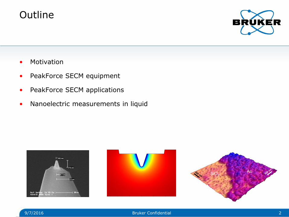
Outline
• Motivation
• PeakForce SECM equipment
• PeakForce SECM applications
• Nanoelectric measurements in liquid
9/7/2016 2 Bruker Confidential
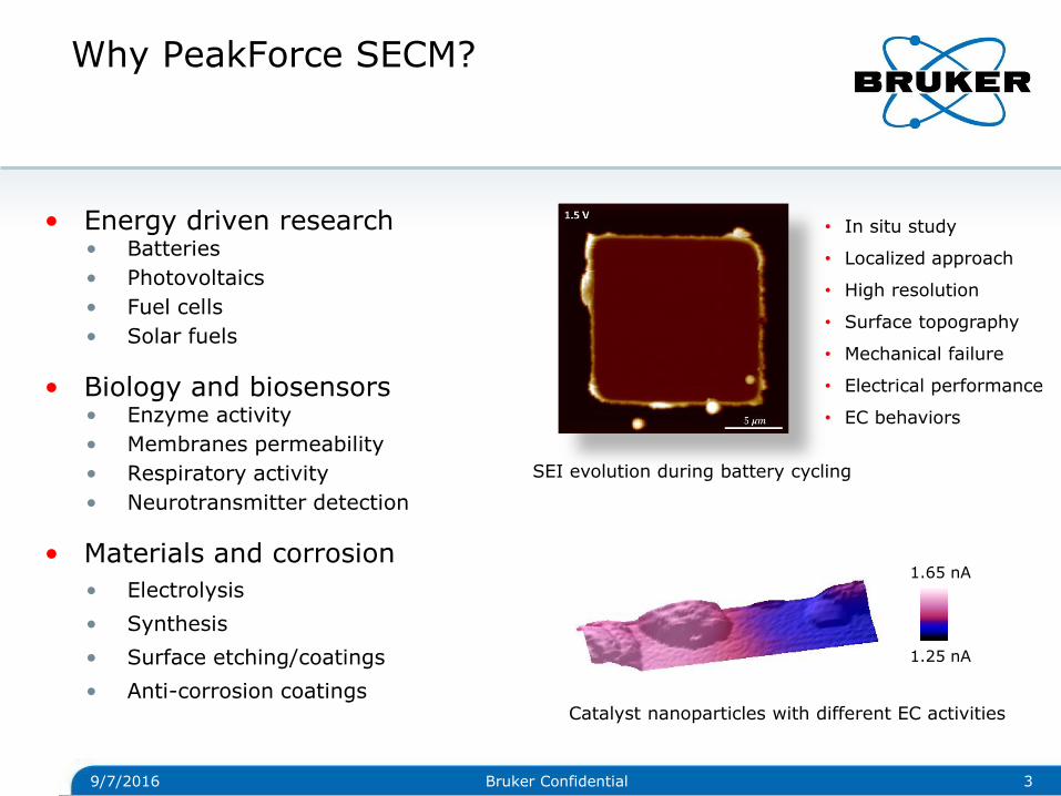
Why PeakForce SECM?
• Energy driven research • Batteries
• Photovoltaics
• Fuel cells
• Solar fuels
• Biology and biosensors • Enzyme activity
• Membranes permeability
• Respiratory activity
• Neurotransmitter detection
• Materials and corrosion
• Electrolysis
• Synthesis
• Surface etching/coatings
• Anti-corrosion coatings
9/7/2016 3 Bruker Confidential
1.65 nA
1.25 nA
SEI evolution during battery cycling
Catalyst nanoparticles with different EC activities
• In situ study
• Localized approach
• High resolution
• Surface topography
• Mechanical failure
• Electrical performance
• EC behaviors
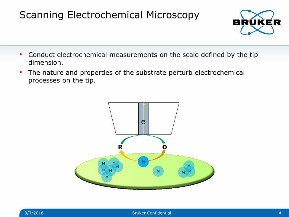
Scanning Electrochemical Microscopy
• Conduct electrochemical measurements on the scale defined by the tip dimension.
• The nature and properties of the substrate perturb electrochemical processes on the tip.
9/7/2016 4 Bruker Confidential
R O
M
M
M M
M
M
M
M M M
M
e
SECM for Local Electrochemistry
9/7/2016 5 Bruker Confidential
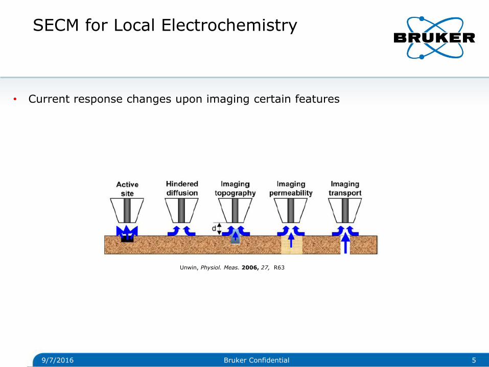
Unwin, Physiol. Meas. 2006, 27, R63
• Current response changes upon imaging certain features
Conductor
Insulator i
SECM for Local Electrochemistry
9/7/2016 6 Bruker Confidential
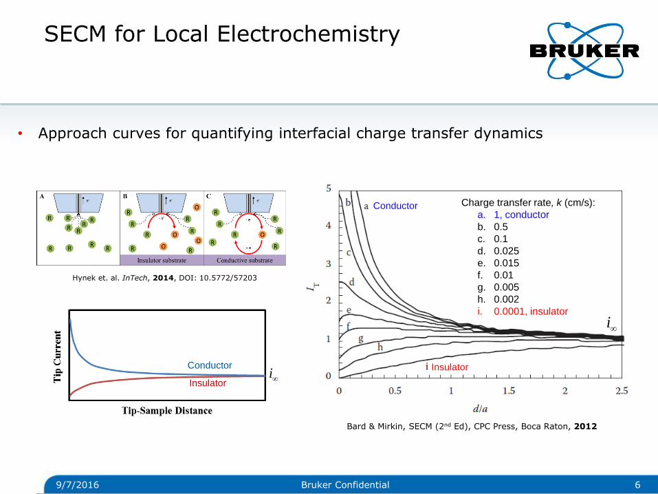
• Approach curves for quantifying interfacial charge transfer dynamics
Bard & Mirkin, SECM (2nd Ed), CPC Press, Boca Raton, 2012
i
Charge transfer rate, k (cm/s):
a. 1, conductor
b. 0.5
c. 0.1
d. 0.025
e. 0.015
f. 0.01
g. 0.005
h. 0.002
i. 0.0001, insulator
Conductor
Insulator
Hynek et. al. InTech, 2014, DOI: 10.5772/57203
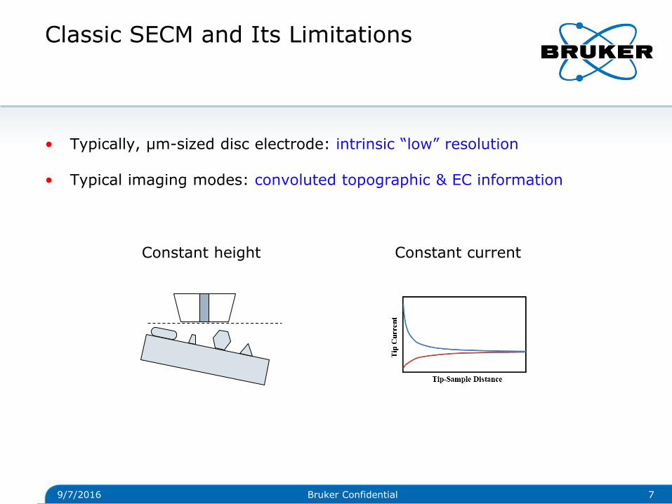
• Typically, µm-sized disc electrode: intrinsic “low” resolution
• Typical imaging modes: convoluted topographic & EC information
Classic SECM and Its Limitations
9/7/2016 7 Bruker Confidential
Constant height Constant current
AFM Based SECM
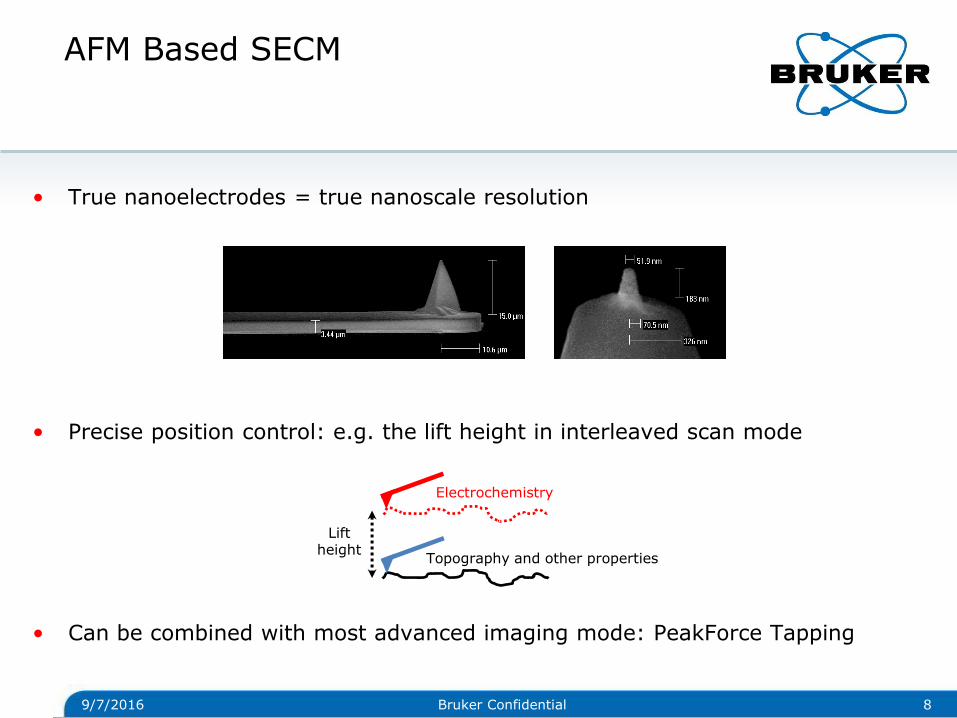
• True nanoelectrodes = true nanoscale resolution
• Precise position control: e.g. the lift height in interleaved scan mode
• Can be combined with most advanced imaging mode: PeakForce Tapping
9/7/2016 8 Bruker Confidential
Lift height
Topography and other properties
Electrochemistry
PeakForce Tapping
9/7/2016 9 Bruker Confidential
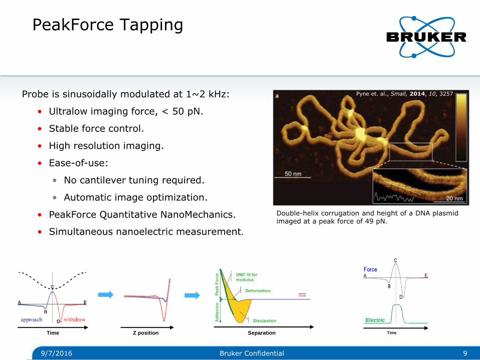
Probe is sinusoidally modulated at 1~2 kHz:
• Ultralow imaging force, < 50 pN.
• Stable force control.
• High resolution imaging.
• Ease-of-use:
• No cantilever tuning required.
• Automatic image optimization.
• PeakForce Quantitative NanoMechanics.
• Simultaneous nanoelectric measurement.
Time Z position Separation
Electric
Time
Double-helix corrugation and height of a DNA plasmid imaged at a peak force of 49 pN.
Pyne et. al., Small, 2014, 10, 3257
PeakForce EC-AFM
9/7/2016 10 Bruker Confidential
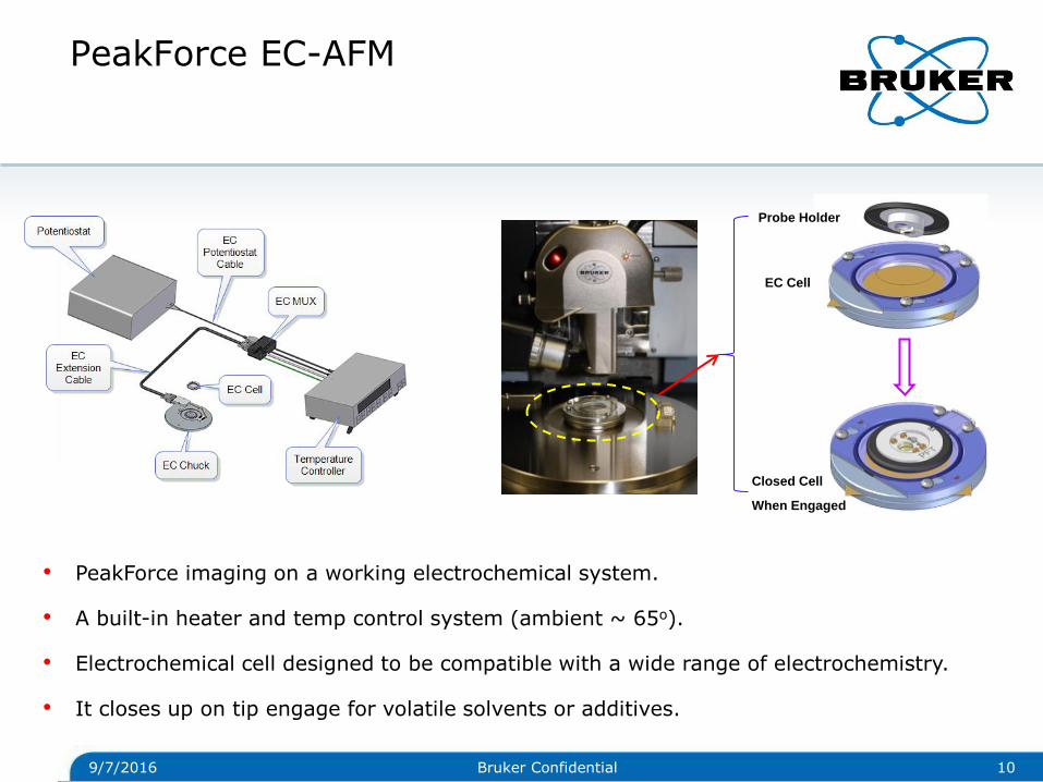
Probe Holder
EC Cell
Closed Cell
When Engaged
• PeakForce imaging on a working electrochemical system.
• A built-in heater and temp control system (ambient ~ 65o).
• Electrochemical cell designed to be compatible with a wide range of electrochemistry.
• It closes up on tip engage for volatile solvents or additives.
PeakForce EC-AFM in Glovebox
9/7/2016 11 Bruker Confidential
PeakForce EC-AFM in Glovebox
9/7/2016 12 Bruker Confidential
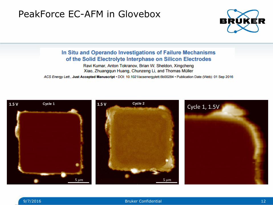
Cycle 1 Cycle 2
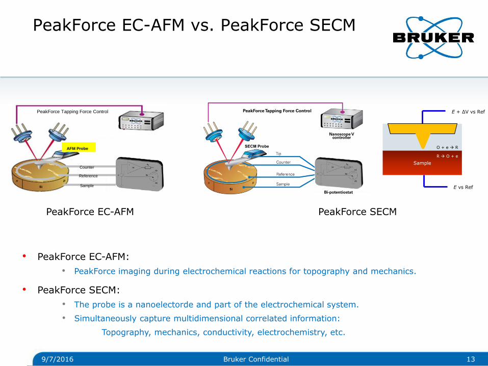
PeakForce EC-AFM vs. PeakForce SECM
9/7/2016 13 Bruker Confidential
AFM Probe
Counter
Reference
Sample
PeakForce Tapping Force Control
• PeakForce EC-AFM:
• PeakForce imaging during electrochemical reactions for topography and mechanics.
• PeakForce SECM:
• The probe is a nanoelectorde and part of the electrochemical system.
• Simultaneously capture multidimensional correlated information:
Topography, mechanics, conductivity, electrochemistry, etc.
PeakForce EC-AFM PeakForce SECM
Sample
E vs Ref
E + ΔV vs Ref
O + e R
R O + e
SECM Probe
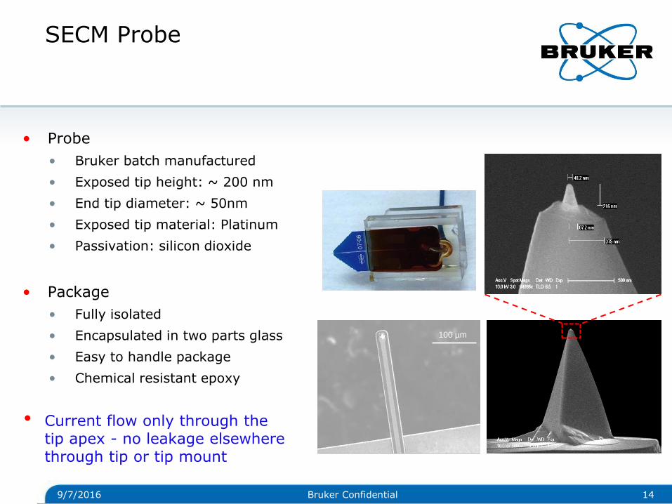
• Probe
• Bruker batch manufactured
• Exposed tip height: ~ 200 nm
• End tip diameter: ~ 50nm
• Exposed tip material: Platinum
• Passivation: silicon dioxide
• Package
• Fully isolated
• Encapsulated in two parts glass
• Easy to handle package
• Chemical resistant epoxy
9/7/2016 14 Bruker Confidential
100 µm
• Current flow only through the tip apex - no leakage elsewhere through tip or tip mount
SECM Probe: Nanoelectrode
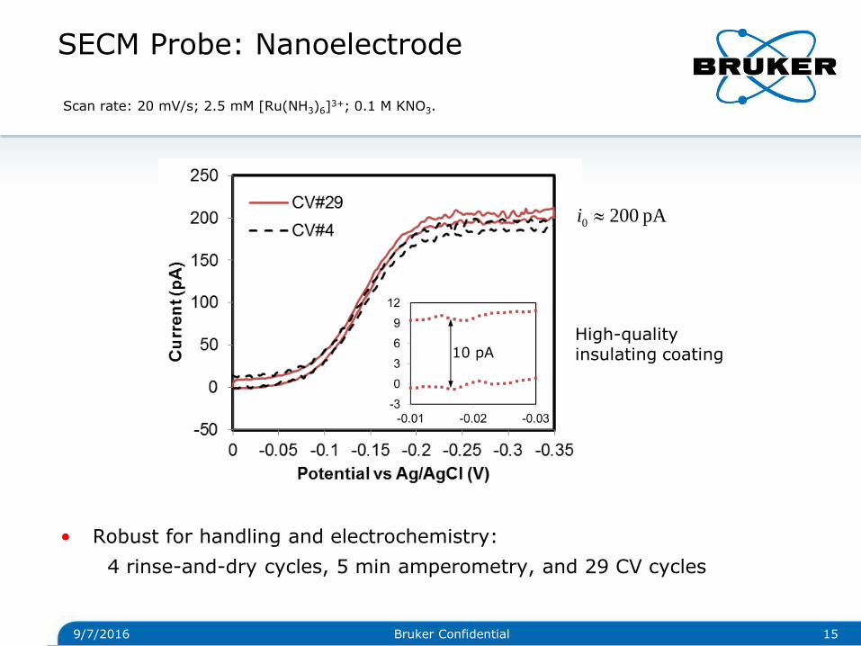
• Robust for handling and electrochemistry:
4 rinse-and-dry cycles, 5 min amperometry, and 29 CV cycles
9/7/2016 15 Bruker Confidential
10 pA
High-quality insulating coating
Scan rate: 20 mV/s; 2.5 mM [Ru(NH3)6]3+; 0.1 M KNO3.
pA 2000 i
SECM Probe: Nanoelectrode
9/7/2016 16 Bruker Confidential
t
i
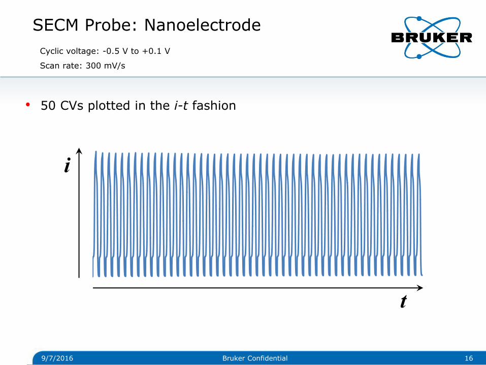
Cyclic voltage: -0.5 V to +0.1 V
Scan rate: 300 mV/s
• 50 CVs plotted in the i-t fashion
SECM Probe: Nanoelectrode
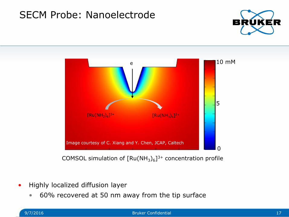
• Highly localized diffusion layer
• 60% recovered at 50 nm away from the tip surface
9/7/2016 17 Bruker Confidential
0
5
10 mM
Image courtesy of C. Xiang and Y. Chen, JCAP, Caltech
[Ru(NH3)6]3+ [Ru(NH3)6]
2+
e
COMSOL simulation of [Ru(NH3)6]3+ concentration profile
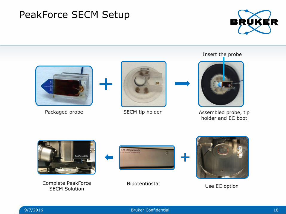
PeakForce SECM Setup
9/7/2016 18 Bruker Confidential
Insert the probe
Complete PeakForce SECM Solution
Packaged probe SECM tip holder Assembled probe, tip holder and EC boot
Bipotentiostat Use EC option
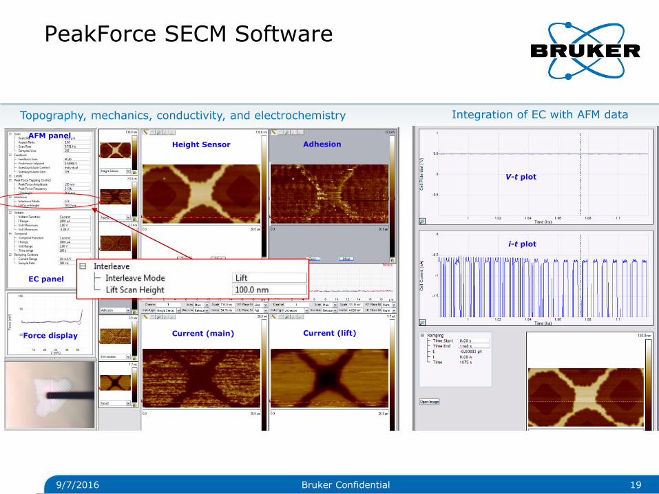
PeakForce SECM Software
9/7/2016 19 Bruker Confidential
Integration of EC with AFM data
V-t plot
i-t plot
Topography, mechanics, conductivity, and electrochemistry
Adhesion Height Sensor
Current (lift) Current (main)
EC panel
AFM panel
Force display
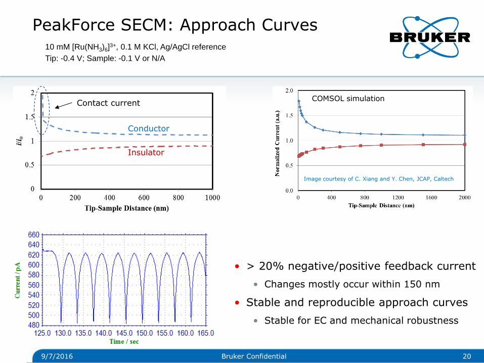
PeakForce SECM: Approach Curves
• > 20% negative/positive feedback current
• Changes mostly occur within 150 nm
• Stable and reproducible approach curves
• Stable for EC and mechanical robustness
9/7/2016 20 Bruker Confidential
Conductor
Insulator
Contact current
10 mM [Ru(NH3)6]3+, 0.1 M KCl, Ag/AgCl reference
Tip: -0.4 V; Sample: -0.1 V or N/A
COMSOL simulation
Image courtesy of C. Xiang and Y. Chen, JCAP, Caltech
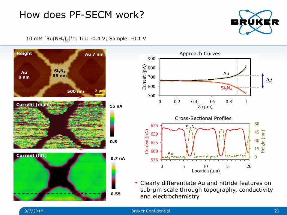
How does PF-SECM work?
9/7/2016 21 Bruker Confidential
Current (main)
0.5
15 nA
Si3N4
55 nm
Au 7 nm Height
Au 0 nm
2 µm 500 nm
Current (lift)
0.55
0.7 nA
Au
Si3N4
Approach Curves
Location (m)0 5 10 15 20
Curr
ent
(pA
)
575
600
625
650
675
Hei
ght
(nm
)
0
15
30
45
60
Au
Si3N4
Cross-Sectional Profiles
• Clearly differentiate Au and nitride features on sub-µm scale through topography, conductivity and electrochemistry
10 mM [Ru(NH3)6]3+; Tip: -0.4 V; Sample: -0.1 V
Δi
Image courtesy of C. Xiang and Y. Chen, Caltech
Outline
• Motivation
• PeakForce SECM equipment
• PeakForce SECM applications
• Nanoelectrode probe
• Nanomesh electrode
• 3D electrochemistry
• Nanoelectrode array
• Interfacial charge transfer dynamics
• Self-assembled monolayer (SAM)
• Surface defect on highly-oriented poly graphite (HOPG)
• Nanoparticle catalysis
• Nanoelectric measurements in liquid
• HOPG: anisotropic conduction in liquid
• Semiconductor/metal junction in liquid
9/7/2016 22 Bruker Confidential
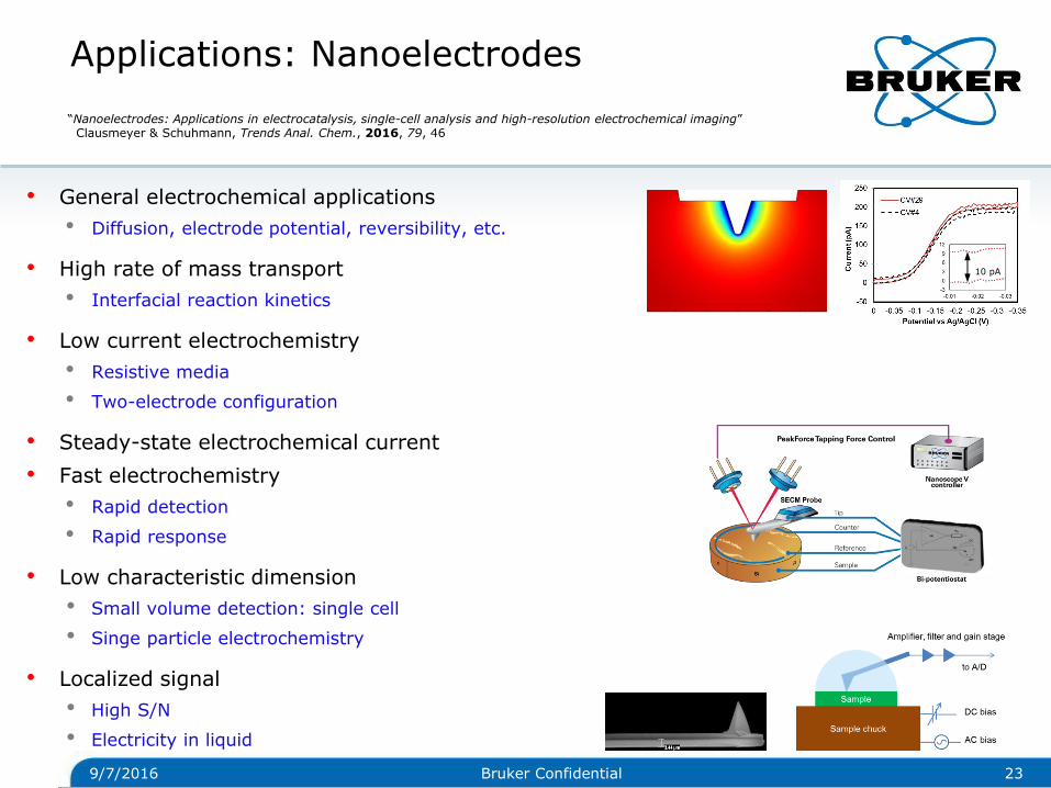
Applications: Nanoelectrodes
9/7/2016 23 Bruker Confidential
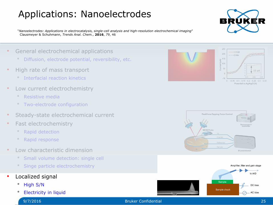
• General electrochemical applications
• Diffusion, electrode potential, reversibility, etc.
• High rate of mass transport
• Interfacial reaction kinetics
• Low current electrochemistry
• Resistive media
• Two-electrode configuration
• Steady-state electrochemical current
• Fast electrochemistry
• Rapid detection
• Rapid response
• Low characteristic dimension
• Small volume detection: single cell
• Singe particle electrochemistry
• Localized signal
• High S/N
• Electricity in liquid
10 pA
Sample
Sample chuck
DC bias
Amplifier, filter and gain stage
to A/D
AC bias
“Nanoelectrodes: Applications in electrocatalysis, single-cell analysis and high-resolution electrochemical imaging” Clausmeyer & Schuhmann, Trends Anal. Chem., 2016, 79, 46
Applications: Nanoelectrodes
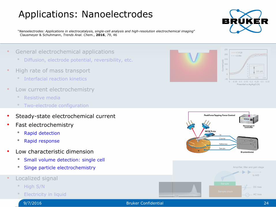
9/7/2016 24 Bruker Confidential
• General electrochemical applications
• Diffusion, electrode potential, reversibility, etc.
• High rate of mass transport
• Interfacial reaction kinetics
• Low current electrochemistry
• Resistive media
• Two-electrode configuration
• Steady-state electrochemical current
• Fast electrochemistry
• Rapid detection
• Rapid response
• Low characteristic dimension
• Small volume detection: single cell
• Singe particle electrochemistry
• Localized signal
• High S/N
• Electricity in liquid
10 pA
Sample
Sample chuck
DC bias
Amplifier, filter and gain stage
to A/D
AC bias
“Nanoelectrodes: Applications in electrocatalysis, single-cell analysis and high-resolution electrochemical imaging” Clausmeyer & Schuhmann, Trends Anal. Chem., 2016, 79, 46
Applications: Nanoelectrodes
9/7/2016 25 Bruker Confidential
• General electrochemical applications
• Diffusion, electrode potential, reversibility, etc.
• High rate of mass transport
• Interfacial reaction kinetics
• Low current electrochemistry
• Resistive media
• Two-electrode configuration
• Steady-state electrochemical current
• Fast electrochemistry
• Rapid detection
• Rapid response
• Low characteristic dimension
• Small volume detection: single cell
• Singe particle electrochemistry
• Localized signal
• High S/N
• Electricity in liquid
10 pA
Sample
Sample chuck
DC bias
Amplifier, filter and gain stage
to A/D
AC bias
“Nanoelectrodes: Applications in electrocatalysis, single-cell analysis and high-resolution electrochemical imaging” Clausmeyer & Schuhmann, Trends Anal. Chem., 2016, 79, 46
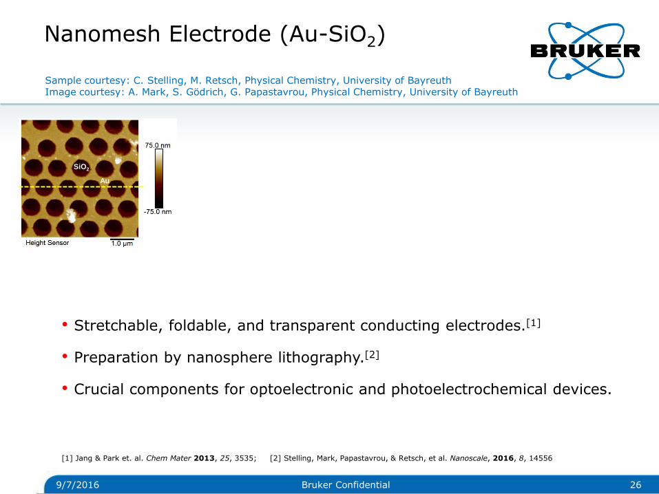
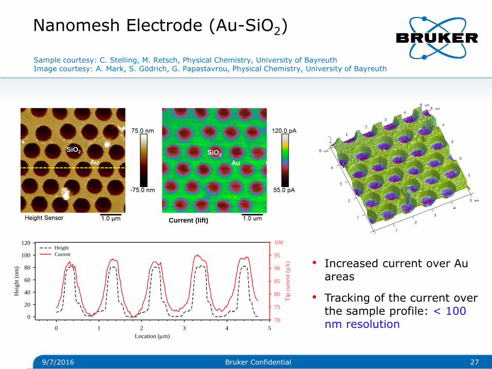
Nanomesh Electrode (Au-SiO2)
9/7/2016 26 Bruker Confidential
SiO2
Au
Sample courtesy: C. Stelling, M. Retsch, Physical Chemistry, University of Bayreuth Image courtesy: A. Mark, S. Gödrich, G. Papastavrou, Physical Chemistry, University of Bayreuth
• Stretchable, foldable, and transparent conducting electrodes.[1]
• Preparation by nanosphere lithography.[2]
• Crucial components for optoelectronic and photoelectrochemical devices.
[1] Jang & Park et. al. Chem Mater 2013, 25, 3535; [2] Stelling, Mark, Papastavrou, & Retsch, et al. Nanoscale, 2016, 8, 14556
Nanomesh Electrode (Au-SiO2)
9/7/2016 27 Bruker Confidential
SiO2
Au
SiO2
Au
Current (lift)
Location (m)
0 1 2 3 4 5
Hei
ght
(nm
)
0
20
40
60
80
100
120
Tip
curr
ent
(pA
)
70
75
80
85
90
95
100Height
Current
Sample courtesy: C. Stelling, M. Retsch, Physical Chemistry, University of Bayreuth Image courtesy: A. Mark, S. Gödrich, G. Papastavrou, Physical Chemistry, University of Bayreuth
• Increased current over Au areas
• Tracking of the current over the sample profile: < 100 nm resolution
Δi
, d
d
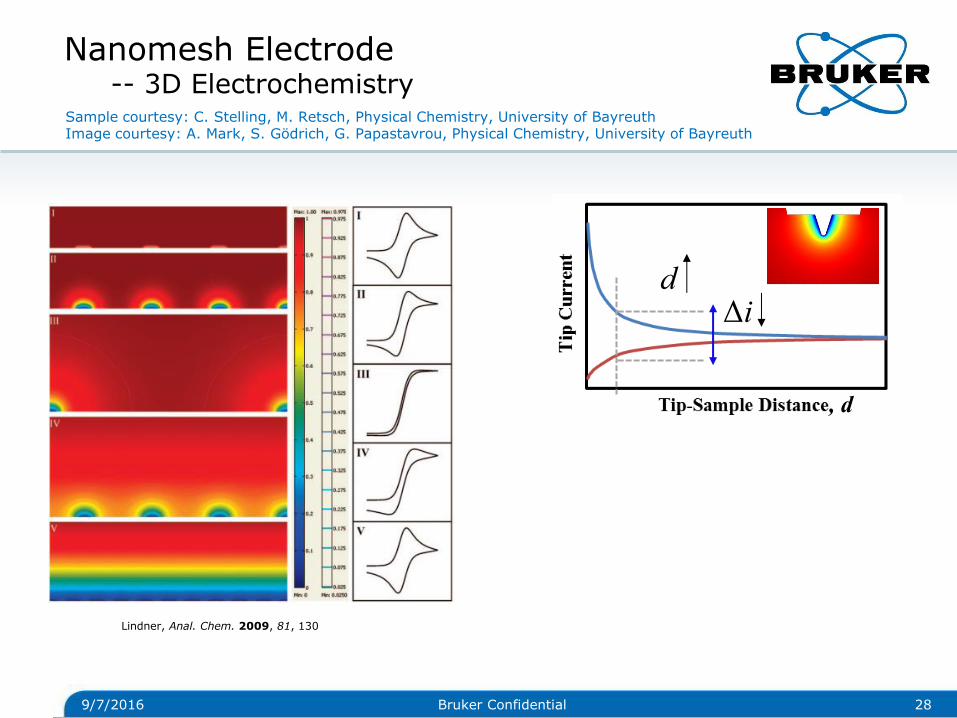
Nanomesh Electrode -- 3D Electrochemistry
9/7/2016 28 Bruker Confidential
Sample courtesy: C. Stelling, M. Retsch, Physical Chemistry, University of Bayreuth Image courtesy: A. Mark, S. Gödrich, G. Papastavrou, Physical Chemistry, University of Bayreuth
Lindner, Anal. Chem. 2009, 81, 130
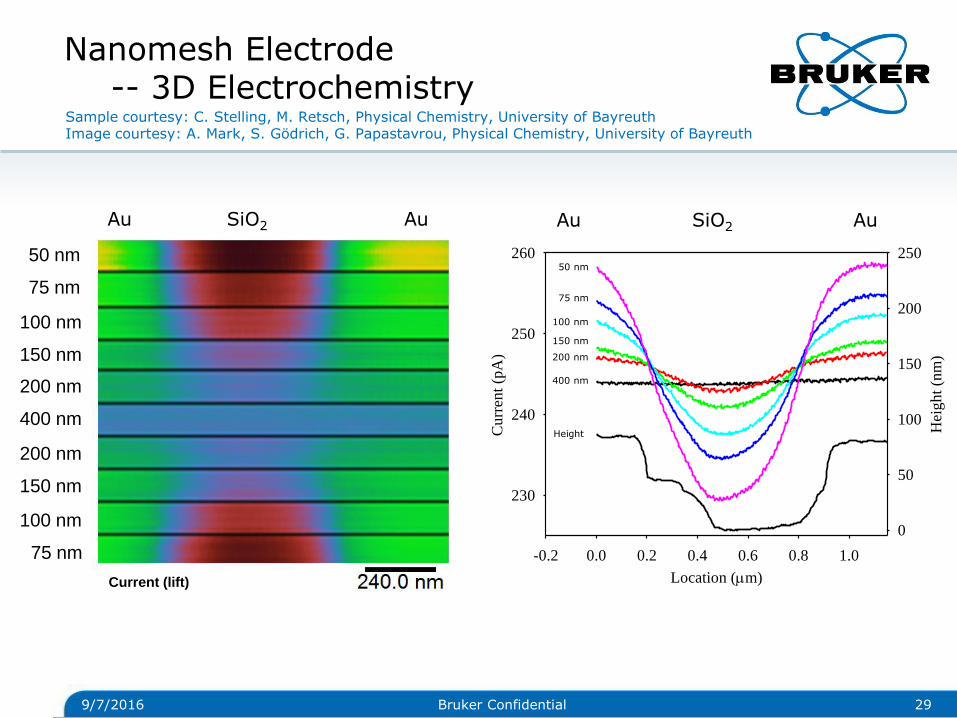
Location (m)
-0.2 0.0 0.2 0.4 0.6 0.8 1.0
Cu
rren
t (p
A)
230
240
250
260
Hei
gh
t (n
m)
0
50
100
150
200
25050 nm
75 nm
100 nm
150 nm
200 nm
400 nm
Height
Nanomesh Electrode -- 3D Electrochemistry
9/7/2016 29 Bruker Confidential
Sample courtesy: C. Stelling, M. Retsch, Physical Chemistry, University of Bayreuth Image courtesy: A. Mark, S. Gödrich, G. Papastavrou, Physical Chemistry, University of Bayreuth
50 nm
75 nm
100 nm
150 nm
200 nm
400 nm
200 nm
150 nm
100 nm
75 nm
Current (lift)
Au SiO2 Au Au SiO2 Au
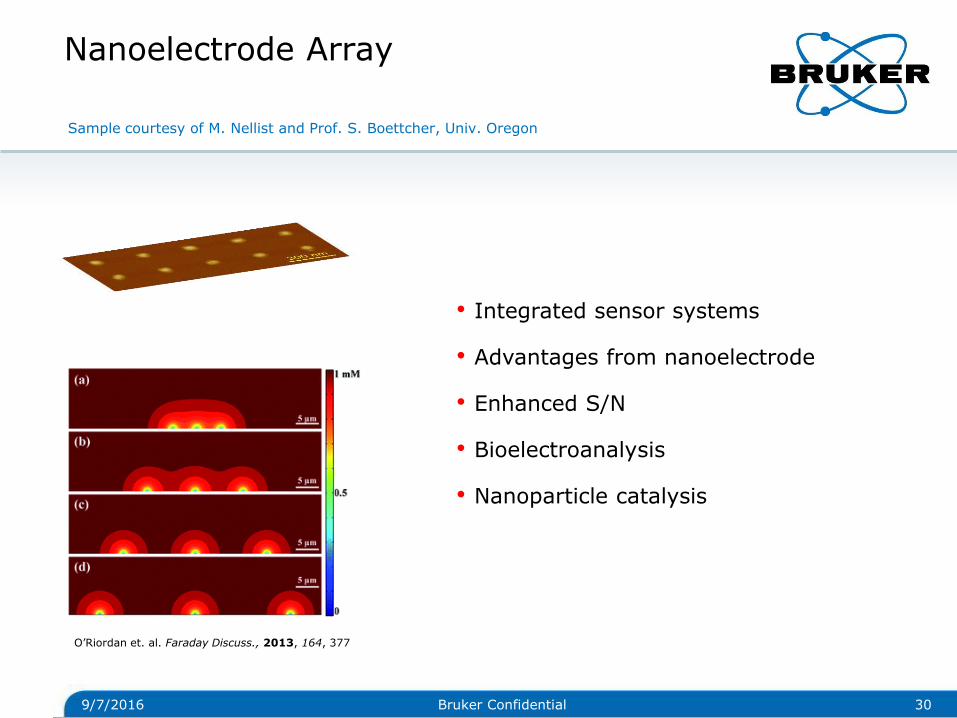
Nanoelectrode Array
9/7/2016 30 Bruker Confidential
• Integrated sensor systems
• Advantages from nanoelectrode
• Enhanced S/N
• Bioelectroanalysis
• Nanoparticle catalysis
O’Riordan et. al. Faraday Discuss., 2013, 164, 377
Sample courtesy of M. Nellist and Prof. S. Boettcher, Univ. Oregon
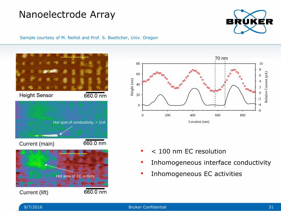
Nanoelectrode Array
9/7/2016 31 Bruker Confidential
• < 100 nm EC resolution
• Inhomogeneous interface conductivity
• Inhomogeneous EC activities
Current (main)
Current (lift)
Hot spot of conductivity, > 1nA
Hot area of EC activity
Location (nm)
0 200 400 600 800
Hei
gh
t (n
m)
0
20
40
60
80
Rel
ativ
e C
urr
ent
(pA
)
-6
-4
-2
0
2
4
6
8
10
70 nm
Sample courtesy of M. Nellist and Prof. S. Boettcher, Univ. Oregon
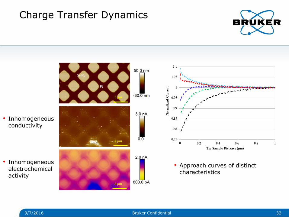
Charge Transfer Dynamics
9/7/2016 32 Bruker Confidential
3 µm
3 µm
3 µm
Si3N4
Pt
• Inhomogeneous conductivity
• Inhomogeneous electrochemical activity
• Approach curves of distinct characteristics
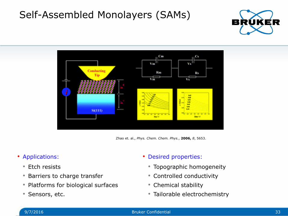
• Applications:
• Etch resists
• Barriers to charge transfer
• Platforms for biological surfaces
• Sensors, etc.
Self-Assembled Monolayers (SAMs)
9/7/2016 33 Bruker Confidential
5 µm
Zhao et. al., Phys. Chem. Chem. Phys., 2006, 8, 5653.
• Desired properties:
• Topographic homogeneity
• Controlled conductivity
• Chemical stability
• Tailorable electrochemistry
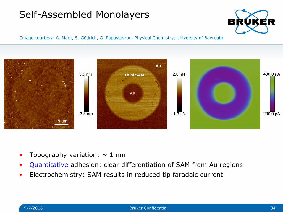
• Topography variation: ~ 1 nm
• Quantitative adhesion: clear differentiation of SAM from Au regions
• Electrochemistry: SAM results in reduced tip faradaic current
Self-Assembled Monolayers
9/7/2016 34 Bruker Confidential
Image courtesy: A. Mark, S. Gödrich, G. Papastavrou, Physical Chemistry, University of Bayreuth
5 µm
Au
Thiol SAM
Au
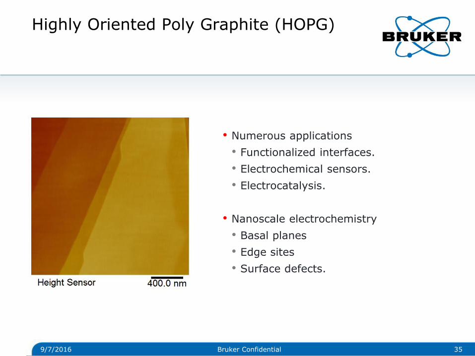
Highly Oriented Poly Graphite (HOPG)
9/7/2016 35 Bruker Confidential
• Numerous applications
• Functionalized interfaces.
• Electrochemical sensors.
• Electrocatalysis.
• Nanoscale electrochemistry
• Basal planes
• Edge sites
• Surface defects.
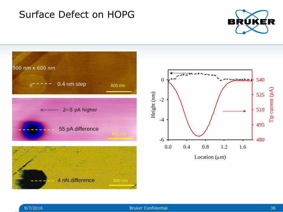
Surface Defect on HOPG
9/7/2016 36 Bruker Confidential
Location (m)
0.0 0.4 0.8 1.2 1.6H
eig
ht
(nm
)
-6
-4
-2
0
Tip
cu
rren
t (p
A)
480
495
510
525
5400.4 nm step
55 pA difference
4 nN difference
800 nm
800 nm
800 nm
900 nm x 600 nm
2~5 pA higher
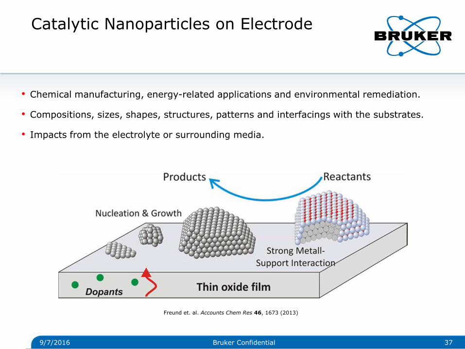
Catalytic Nanoparticles on Electrode
9/7/2016 37 Bruker Confidential
• Chemical manufacturing, energy-related applications and environmental remediation.
• Compositions, sizes, shapes, structures, patterns and interfacings with the substrates.
• Impacts from the electrolyte or surrounding media.
Freund et. al. Accounts Chem Res 46, 1673 (2013)
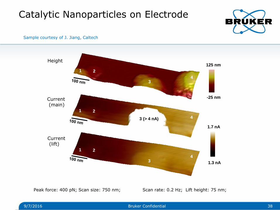
Catalytic Nanoparticles on Electrode
9/7/2016 38 Bruker Confidential
1 2
3 (> 4 nA) 4
1 2
3 4
Current (main)
Current (lift)
1.3 nA
1.7 nA
1 2
3 4
Height
-25 nm
125 nm
Peak force: 400 pN; Scan size: 750 nm; Scan rate: 0.2 Hz; Lift height: 75 nm;
Sample courtesy of J. Jiang, Caltech
Outline
• Motivation
• PeakForce SECM equipment
• PeakForce SECM applications
• Nanoelectrode probe
• Nanomesh electrode
• 3D electrochemistry
• Nanoelectrode array
• Interfacial charge transfer dynamics
• Self-assembled monolayer (SAM)
• Surface defect on highly-oriented poly graphite (HOPG)
• Nanoparticle catalysis
• Nanoelectric measurements in liquid
• HOPG: anisotropic conduction in liquid
• Semiconductor/metal junction in liquid
9/7/2016 39 Bruker Confidential
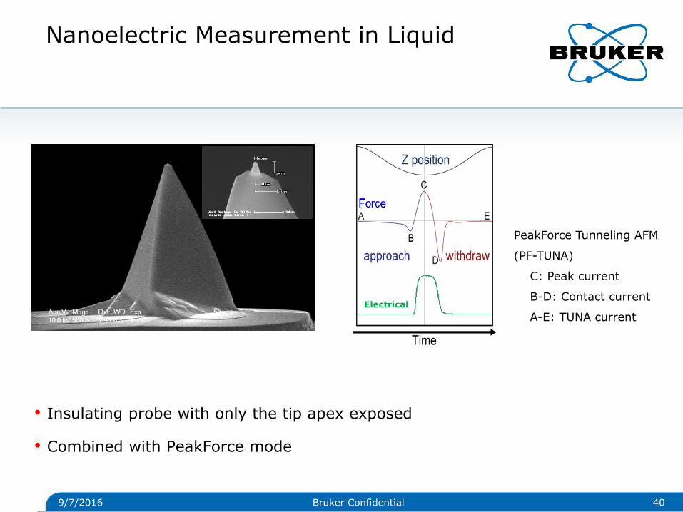
Nanoelectric Measurement in Liquid
• Insulating probe with only the tip apex exposed
• Combined with PeakForce mode
9/7/2016 40 Bruker Confidential
Electrical
PeakForce Tunneling AFM
(PF-TUNA)
C: Peak current
B-D: Contact current
A-E: TUNA current
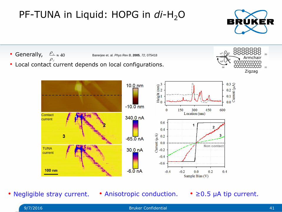
PF-TUNA in Liquid: HOPG in di-H2O
9/7/2016 41 Bruker Confidential
• Generally,
• Local contact current depends on local configurations.
40//
Armchair
Zigzag
• Negligible stray current.
Banerjee et. al. Phys Rev B, 2005, 72, 075418
Contact
current
TUNA
current
• Anisotropic conduction. • ≥0.5 µA tip current.
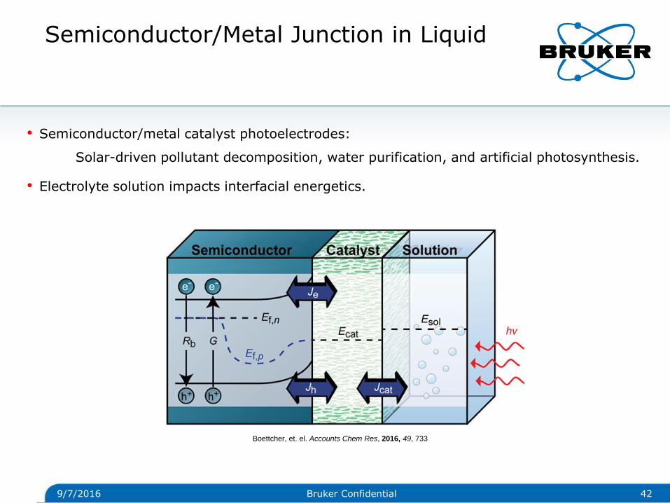
Semiconductor/Metal Junction in Liquid
9/7/2016 42 Bruker Confidential
• Semiconductor/metal catalyst photoelectrodes:
Solar-driven pollutant decomposition, water purification, and artificial photosynthesis.
• Electrolyte solution impacts interfacial energetics.
Boettcher, et. el. Accounts Chem Res, 2016, 49, 733
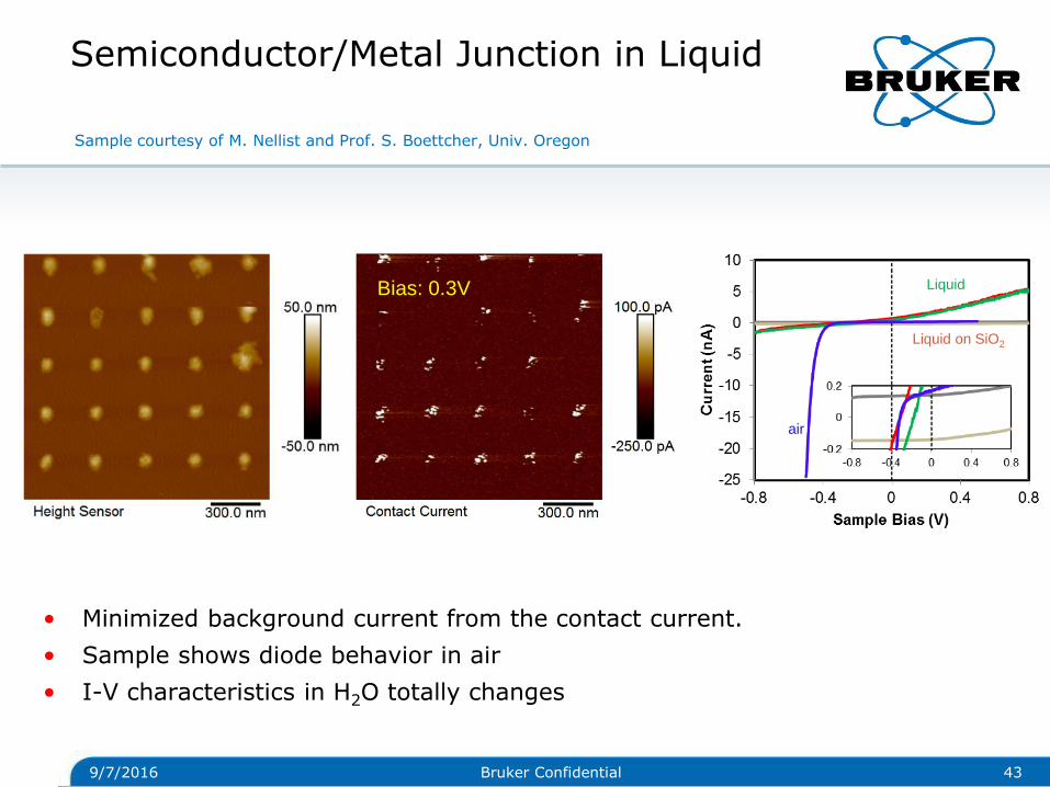
Semiconductor/Metal Junction in Liquid
• Minimized background current from the contact current.
• Sample shows diode behavior in air
• I-V characteristics in H2O totally changes
9/7/2016 43 Bruker Confidential
Sample courtesy of M. Nellist and Prof. S. Boettcher, Univ. Oregon
air
Liquid
Liquid on SiO2
Bias: 0.3V
Conclusion
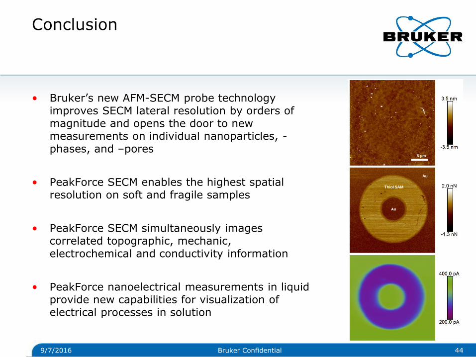
• Bruker’s new AFM-SECM probe technology improves SECM lateral resolution by orders of magnitude and opens the door to new measurements on individual nanoparticles, -phases, and –pores
• PeakForce SECM enables the highest spatial resolution on soft and fragile samples
• PeakForce SECM simultaneously images correlated topographic, mechanic, electrochemical and conductivity information
• PeakForce nanoelectrical measurements in liquid provide new capabilities for visualization of electrical processes in solution
9/7/2016 44 Bruker Confidential
5 µm
Au
Thiol SAM
Au
Acknowledgements
9/7/2016 45 Bruker Confidential
Sebastian Gödrich Andreas Mark Prof. Georg Papastavrou Christian Stelling Prof. Markus Retsch
• Universität Bayreuth
• Joint Center for Artificial Photosynthesis (Caltech); CCI Solar (Caltech)
Dr. Chengxiang (CX) Xiang Dr. Bruce Brunschwig Yikai (Katie) Chen Jingjing (Jessica) Jiang
• University of Oregon
Prof. Shannon Boettcher Michael Nellist
• University of Leeds
Prof. Christoph Wälti Dr. Andrew Lee Dr. William Morton
Ravi Kumar Prof. Brian Sheldon Dr. Anton Tokranov
• Brown University
Dr. Xingcheng Xiao
• General Motors R&D

© Copyright Bruker Corporation. All rights reserved.
www.bruker.com
46 Bruker Product Information


