• To experimentally explore the effect of Capacitors andInductors on the phase of voltages and currents in a circuit
Overview
This experiment is designed to demonstrate the analysis of R-C, R-L and R-L-C circuits by
the use of phasors. A summary of phasors and phasor analysis of sinusoidal steady state is presented in section 2.The prelab exercises are designed to promote familiarity with the concepts and involve
calculations of the values of several elements that will be used in the experiments.The three actual laboratory experiments are designed to verify the concepts by direct
measurement of voltages, currents and resistances. The difference of a real and an idealinductor is made clear with the measurement of the associated d.c. resistance and its
incorporation in the calculation of the resistance value to be used experimentally.
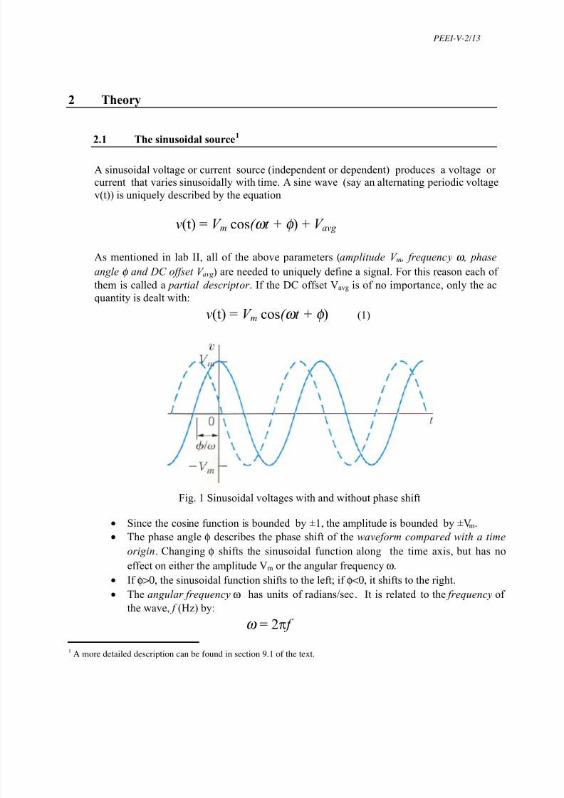
A sinusoidal voltage or current source (independent or dependent) produces a voltage or current that varies sinusoidally with time. A sine wave (say an alternating periodic voltage
v(t)) is uniquely described by the equation
v(t) = V m cos( ! t + " ) + V avg
As mentioned in lab II, all of the above parameters (amplitude V m , frequency ! , phase
angle " and DC offset V avg ) are needed to uniquely define a signal. For this reason each of
them is called a partial descriptor . If the DC offset Vavg is of no importance, only the ac
quantity is dealt with:
v(t) = V m cos( ! t + " ) (1)
Fig. 1 Sinusoidal voltages with and without phase shift
• Since the cosine function is bounded by ±1, the amplitude is bounded by ±Vm.
• The phase angle " describes the phase shift of the waveform compared with a time
origin. Changing " shifts the sinusoidal function along the time axis, but has no
effect on either the amplitude Vm or the angular frequency !.
• If ">0, the sinusoidal function shifts to the left; if "<0, it shifts to the right.
• The angular frequency ! has units of radians/sec. It is related to the frequency of
the wave, f (Hz) by:
! = 2! f
1 A more detailed description can be found in section 9.1 of the text.
Using the Euler identity, e±j# = cos(# ) ± jsin(# )
Eq. 1 can be written as follows:
v(t ) = V m $ e j( ! t + " ) = V m $ e
j! t e j " = $ (V me
j " )e j! t The complex number V me
j" is called the phasor representation or the phasor transform of
v(t ). Phasors include only two of the partial descriptors e.g. they convey no frequencyinformation but they greatly simplify notation. For example Eq. 1 can be represented in the
phasor domain as follows3:
V = V m%"
2.3 The passive circuit elements in the Phasor Domain4
If i(t) is the current flowing through a resistor, inductor, or a capacitor, and
i(t) = I m cos( ! t + # i) then in phasor notation I = I m % # iand the voltage in the phasor domain in each case is:
a- Across a resistor:
V = R I = RI m % # i (2)
b- Across an inductor:
V = ( j! L) I = ! LI m % # i +90º (3)
c- Across a capacitor:
V = (1/j! C) I = -(j! C) I = I m / ! C % # i -90º (4)
2 A more detailed description can be found in section 9.3 of the text.3 In agreement with the notation of the text, phasors and only phasors will be represented by capital bold symbols
throughout this lab.4 The subject is treated in more detail in section 9.4 of the text.
Refer to Fig.3 and compute R and C for Z = 2556%-38.5o Ω at f = 1000Hz. Note that
Z = R !j
" C = R
2+
1
" 2C
2%! tan!1 1
" CR
# $ %
& ' (
++
-
C
Rs
+
+
-
-
C
R
3.2 Maximum power A
For the following source circuit, design a load circuit that will extract maximum power fromit. Your design should minimize the number of parts and must be within 5% of transferring
maximum power to the load.Calculate the complex power that is delivered to the load.
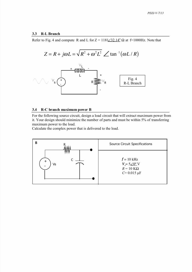
Refer to Fig. 4 and compute R and L for Z = 1181%32.14o Ω at f=1000Hz. Note that
Z = R + j ! L = R2+!
2 L
2 % tan!1
" L / R( )
-
++
-R
L
s
+
+ -L
R
3.4 R-C branch maximum power B
For the following source circuit, design a load circuit that will extract maximum power fromit. Your design should minimize the number of parts and must be within 5% of transferring
maximum power to the load.Calculate the complex power that is delivered to the load.
Various circuit elements to be determined by students
4.1 R-C branch
a. With the values of R and C as computed in pre-lab exercise 3.1, build the circuitof Fig.3.
b. Connect the DVM (switched to AC) across the resistor and adjust the oscillator 7
output8 until V R has the proper value that corresponds to a current of 1mAflowing through the circuit.
c. Measure V s , V R, and V C .
d.
Display the time domain signals v s(t) and v R(t) corresponding to V s and V R on theoscilloscope, and download them to your floppy disk.
e. Measure the phase. The oscilloscope can automatically calculate the phase
difference angle # between the phasors V s and V R in the following way:
- press the Quick Meas button
- press the 2nd
soft key to select phase- press the 3
rdsoft key to measure the phase difference between the two
signals
6 Throughout this experiment, large resistance values will be used; thus, the 50Ω internal impedance of the function
generator can be neglected.7 “Oscillator” is routinely used for any source of ac voltage (here the Function Generator).8 The oscillator output and the oscilloscope input have a common ground connection, consequently a component
voltage cannot be displayed properly on the scope unless that component is also connected to the common
ground. Make sure that you build your circuits exactly as shown in the figures.
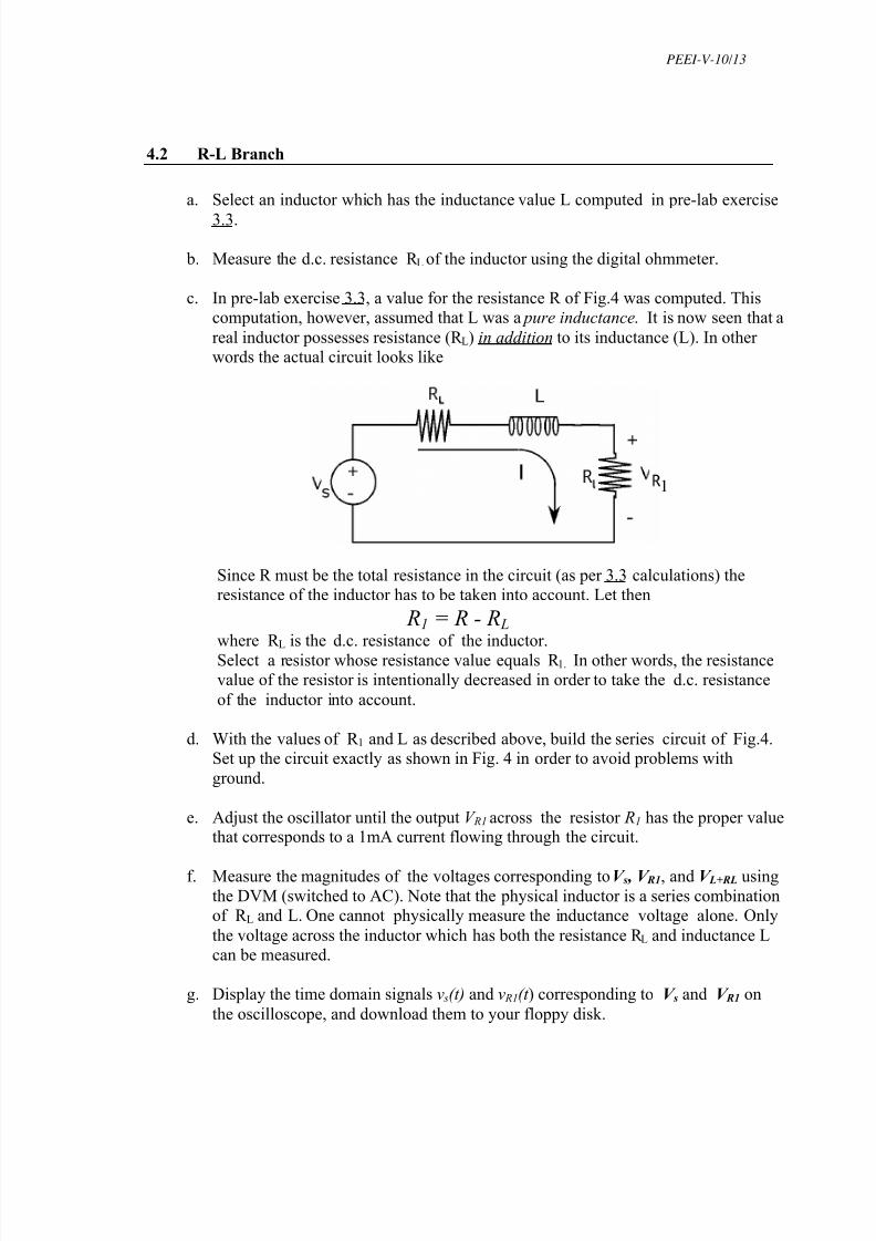
a. Select an inductor which has the inductance value L computed in pre-lab exercise
3.3.
b. Measure the d.c. resistance R L of the inductor using the digital ohmmeter.
c. In pre-lab exercise 3.3, a value for the resistance R of Fig.4 was computed. Thiscomputation, however, assumed that L was a pure inductance. It is now seen that a
real inductor possesses resistance (R L) in addition to its inductance (L). In other words the actual circuit looks like
Since R must be the total resistance in the circuit (as per 3.3 calculations) theresistance of the inductor has to be taken into account. Let then
R1 = R - R L
where R L is the d.c. resistance of the inductor.
Select a resistor whose resistance value equals R 1. In other words, the resistancevalue of the resistor is intentionally decreased in order to take the d.c. resistance
of the inductor into account.
d. With the values of R 1 and L as described above, build the series circuit of Fig.4.Set up the circuit exactly as shown in Fig. 4 in order to avoid problems with
ground.
e. Adjust the oscillator until the output V R1 across the resistor R1 has the proper valuethat corresponds to a 1mA current flowing through the circuit.
f. Measure the magnitudes of the voltages corresponding to V s , V R1, and V L+RL usingthe DVM (switched to AC). Note that the physical inductor is a series combinationof R L and L. One cannot physically measure the inductance voltage alone. Only
the voltage across the inductor which has both the resistance R L and inductance Lcan be measured.
g. Display the time domain signals v s(t) and v R1(t ) corresponding to V s and V R1 on
the oscilloscope, and download them to your floppy disk.
h. Measure the phase angle # between V s and V R1 using the method explained in
Section 4.1.e.
4.3 R-L-C Branch
a. Measure the d.c. resistance R L of the inductor whose inductance value is L =100mH.
b. Build the R-L-C series circuit of Fig. 5 by using the R and C values as computed
in pre-lab exercise 3.5. Make sure that the value of resistance R is decreased to R1
= R - R L by the d.c. resistance of the inductor as in 4.2.c.
c. Follow the steps in Section 4.1 and measure Vs, VR1, VL+RL, VC, and the phaseangle # between V s and V R1; download the waveforms v s(t) and v R1(t )
corresponding to V s and V R1 from the oscilloscope.
d. At resonance the reactance X is zero and the impedance is purely resistive.
Since the imaginary portion of the impedance is zero the phase angle is equal tozero.
Measure the resonant frequency for the circuit of Fig. 5. There are a number of ways of doing so. One way is to tune the frequency of the oscillator until V s and
V R1 are in phase, (i.e. the phase angle between them is zero) by watching v s(t)and v R1(t ).
e. For all frequencies above resonance, phase angles have the same sign and for
frequencies below the resonant point they have the opposite sign. Verify that thisis true over a frequency range of two orders of magnitude extending on both sides
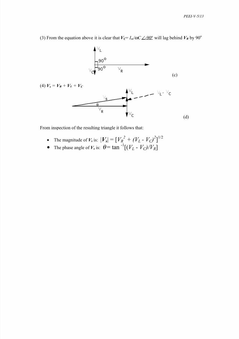
5.1 For the R-C branch shown in Fig.3, do the following:
a.
Tabulate Vs, VR , VC, and # measured in the experiment. b. Submit a copy of the waveforms v s(t) and v R(t ) of V s and V Rc. Prepare a phasor diagram to scale that represents in phasor domain
V s = V R + V C .d. Calculate the phase angle # in three different ways:
# = -tan-1
(V C /V R) = -sin-1
(V C /V s) = -cos-1
(V R /V s)Compare # calculated with # measured.
e. Calculate the average power 9, P, in two different ways:
P = V R2 /R = V s I cos#
where # is the measured phase angle.
f. Does V R lead or lag V s?g. For the circuit of Fig. A in pre-lab exercise 3.2, what is the load that
consumes the maximum power and what is that value of maximum power?
5.2 For the R-L branch shown in Fig.4, do the following:
a. Tabulate Vs, VR1, VL+RL, and # measured.
b. Submit a copy of the waveforms v s(t) and v R1(t ) of V R1 and V s.
c. Prepare a phasor diagram to scale. Take the effect of the d.c. resistance of the inductor into account.
d.
From the phasor diagram, determine the phase angle # in three different waysas in item 5.1.d. Compare with the measured one.
e. Calculate the average power, P, in two different ways as in 5.1.e.f. Does V R lead or lag V s?
h. For the circuit of Fig. B in pre-lab exercise 3.4, what is the load thatconsumes the maximum power and what is that value of maximum power.
5.3 For the R-L-C branch in Fg. 5, repeat 5.2 (a-f) for the impedance Z used in performing
the experiment. Do not forget to take into account the d.c. resistance R L of the inductor L in all calculations.
5.4 With v s(t) = 10sin(2' ft ) Volts where f =1KHz, use PSpice to plot v s(t) and v R(t ) for thethree circuits in figures 3, 4, and 5. Show 2 to 4 periods of the waveforms in your plot.(Hint: Use the TRAN. command.)
9 For detailed discussion on average power see section 10.2 of the text.