Performance analysis of radix-4 adders Shahzad Asif a,n , Mark Vesterbacka b a Department of EE, COMSATS IIT, 44000 Islamabad, Pakistan b Department of EE, Link¨ oping University, SE-581 83 Link¨ oping, Sweden article info Article history: Received 30 May 2011 Received in revised form 28 September 2011 Accepted 30 September 2011 Available online 13 October 2011 Keywords: CMOS full adder Radix-4 adder Power-delay product Energy-delay product Carry-based adder abstract We present a radix-4 static CMOS full adder circuit that reduces the propagation delay, PDP, and EDP in carry-based adders compared with using a standard radix-2 full adder solution. The improvements are obtained by employing carry look-ahead technique at the transistor level. Spice simulations using 45 nm CMOS technology parameters with a power supply voltage of 1.1 V indicate that the radix-4 circuit is 24% faster than a 2-bit radix-2 ripple carry adder with slightly larger transistor count, whereas the power consumption is almost the same. A second scheme for radix-2 and radix-4 adders that have a reduced number of transistors in the carry path is also investigated. Simulation results also confirm that the radix-4 adder gives better performance as compared to a standard 2-bit CLA. 32-Bit ripple carry, 2-stage carry select, variable size carry select, and carry skip adders are implemented with the different full adders as building blocks. There are PDP savings, with one exception, for the 32-bit adders in the range 8–18% and EDP savings in the range 21–53% using radix-4 as compared to radix-2. & 2011 Elsevier B.V. All rights reserved. 1. Introduction Addition is the most basic and most frequently used operation in digital circuit design [1,2]. Due to this reason, a large number of adder architectures have been designed to accommodate the requirements of different applications. Common parameters that measure the performance of a circuit are speed, power, area, power-delay product (PDP), and energy-delay product (EDP), where the PDP represents the energy dissipation per switching event and the EDP is a commonly used measure for energy- performance trade-off [3,4]. On the basis of area and speed, we can divide the adders in three major categories. The ripple carry adder (RCA) is the slowest architecture with the least number of transistors. The carry look-ahead adder (CLA) is the fastest adder but requires very large area. The carry select adder (CSEL) is used when we need a moderate solution [5–7]; it is faster than RCA but slower than CLA. Extensive research has been done to improve the performance of the full adder (FA), which is the basic building block for large carry-based adders. In [8–11], different architectures have been presented to improve the performance of the FA in terms of speed, power, and energy. In [12], different FA architectures are analyzed and compared with respect to speed, power consumption and PDP. In [13,14], different radix-2 and radix-4 architectures are presented and compared for 64-bit parallel prefix adders with main emphasis on the Kogge–Stone adder. In this work, we design a radix-4 FA instead of the more common radix-2 FA. The radix-4 FA is based on internal carry look-ahead to reduce the carry propagation path in an adder since that path is critical [3]. The main disadvantage of this architecture is a slight increase in transistor count. With the scaling of technology and supply voltage, it is becoming more important to design the circuits having full voltage swing, which results in high noise margins. For low power applications, it is also common to reduce the supply voltage, but doing so will result in even lower noise margins [15]. Static CMOS logic provides high gain and a voltage swing equal to the supply voltage, yielding high noise margins. Hence, the CMOS logic style is a good choice for low power implementation in deep submicron technologies [16], which we have chosen for our design. The paper is organized as follows. In Section 2, we study different FA topologies. In Section 3, two radix-4 FAs are pro- posed. In Sections 4 and 5, we discuss 32-bit adders that are implemented for comparison. Section 6 shows the simulation results of the adders, and the work is concluded in Section 7. 2. FA topology In this work we focus on static CMOS circuits, which provide the high noise margins required for implementation in deep submicron technologies. A popular topology is the mirror FA [12], which is used Contents lists available at SciVerse ScienceDirect journal homepage: www.elsevier.com/locate/vlsi INTEGRATION, the VLSI journal 0167-9260/$ - see front matter & 2011 Elsevier B.V. All rights reserved. doi:10.1016/j.vlsi.2011.09.004 n Corresponding author. E-mail addresses: [email protected] (S. Asif), [email protected] (M. Vesterbacka). INTEGRATION, the VLSI journal 45 (2012) 111–120
Transcript
INTEGRATION, the VLSI journal 45 (2012) 111–120
Contents lists available at SciVerse ScienceDirect
INTEGRATION, the VLSI journal
0167-92
doi:10.1
n Corr
E-m
markv@
journal homepage: www.elsevier.com/locate/vlsi
Performance analysis of radix-4 adders
Shahzad Asif a,n, Mark Vesterbacka b
a Department of EE, COMSATS IIT, 44000 Islamabad, Pakistanb Department of EE, Linkoping University, SE-581 83 Linkoping, Sweden
a r t i c l e i n f o
Article history:
Received 30 May 2011
Received in revised form
28 September 2011
Accepted 30 September 2011Available online 13 October 2011
We present a radix-4 static CMOS full adder circuit that reduces the propagation delay, PDP, and EDP in
carry-based adders compared with using a standard radix-2 full adder solution. The improvements are
obtained by employing carry look-ahead technique at the transistor level. Spice simulations using
45 nm CMOS technology parameters with a power supply voltage of 1.1 V indicate that the radix-4
circuit is 24% faster than a 2-bit radix-2 ripple carry adder with slightly larger transistor count, whereas
the power consumption is almost the same. A second scheme for radix-2 and radix-4 adders that have a
reduced number of transistors in the carry path is also investigated. Simulation results also confirm that
the radix-4 adder gives better performance as compared to a standard 2-bit CLA. 32-Bit ripple carry,
2-stage carry select, variable size carry select, and carry skip adders are implemented with the different
full adders as building blocks. There are PDP savings, with one exception, for the 32-bit adders in the
range 8–18% and EDP savings in the range 21–53% using radix-4 as compared to radix-2.
& 2011 Elsevier B.V. All rights reserved.
1. Introduction
Addition is the most basic and most frequently used operationin digital circuit design [1,2]. Due to this reason, a large number ofadder architectures have been designed to accommodate therequirements of different applications. Common parameters thatmeasure the performance of a circuit are speed, power, area,power-delay product (PDP), and energy-delay product (EDP),where the PDP represents the energy dissipation per switchingevent and the EDP is a commonly used measure for energy-performance trade-off [3,4]. On the basis of area and speed, wecan divide the adders in three major categories. The ripple carryadder (RCA) is the slowest architecture with the least number oftransistors. The carry look-ahead adder (CLA) is the fastest adderbut requires very large area. The carry select adder (CSEL) is usedwhen we need a moderate solution [5–7]; it is faster than RCA butslower than CLA.
Extensive research has been done to improve the performanceof the full adder (FA), which is the basic building block for largecarry-based adders. In [8–11], different architectures have beenpresented to improve the performance of the FA in terms of speed,power, and energy. In [12], different FA architectures are analyzedand compared with respect to speed, power consumption andPDP. In [13,14], different radix-2 and radix-4 architectures are
ll rights reserved.
S. Asif),
presented and compared for 64-bit parallel prefix adders withmain emphasis on the Kogge–Stone adder.
In this work, we design a radix-4 FA instead of the morecommon radix-2 FA. The radix-4 FA is based on internal carrylook-ahead to reduce the carry propagation path in an adder sincethat path is critical [3]. The main disadvantage of this architectureis a slight increase in transistor count.
With the scaling of technology and supply voltage, it isbecoming more important to design the circuits having fullvoltage swing, which results in high noise margins. For low powerapplications, it is also common to reduce the supply voltage,but doing so will result in even lower noise margins [15]. StaticCMOS logic provides high gain and a voltage swing equal to thesupply voltage, yielding high noise margins. Hence, the CMOSlogic style is a good choice for low power implementation indeep submicron technologies [16], which we have chosen forour design.
The paper is organized as follows. In Section 2, we studydifferent FA topologies. In Section 3, two radix-4 FAs are pro-posed. In Sections 4 and 5, we discuss 32-bit adders that areimplemented for comparison. Section 6 shows the simulationresults of the adders, and the work is concluded in Section 7.
2. FA topology
In this work we focus on static CMOS circuits, which provide thehigh noise margins required for implementation in deep submicrontechnologies. A popular topology is the mirror FA [12], which is used
S. Asif, M. Vesterbacka / INTEGRATION, the VLSI journal 45 (2012) 111–120112
as the base topology for our designs. Two different mirror FA circuitsare examined.
Fig. 1 shows the typical 28-transistor mirror FA. The carry isgenerated first since it is on the critical path, and then it is reusedin the sum generation to obtain low area.
Another mirror FA that consists of 24 transistors is shown inFig. 2 [17]. Compared to the previous FA, the transistor count isreduced for the sum generation while the circuitry for the carrygeneration is the same as in Fig. 1.
Both FAs implement the same Boolean function, which is givenin Eqs. (1) and (2):
Cout ¼ ðAþBÞCinþAB ð1Þ
Sum¼ Cout AþCout BþCout CinþABCin ð2Þ
The circuits are designed using 45 nm CMOS technologyparameters [18] and simulated in Spice with a power supplyvoltage of 1.1 V. Widths of all NMOS and PMOS devices are set to0.1 mm and 0.2 mm, respectively. For power dissipation weapplied pulses with time periods 6 ns, 12 ns, and 24 ns to inputsA, B, and Cin, respectively. An inverter is used as load on the carryand sum output in the simulations of the delay and energydissipation, which are reported in Table 1. Widths of NMOS andPMOS for this inverter are set to 0.1 mm and 0.2 mm, respectively.
From the results given in Table 1, it appears that the 28-transistor FA is better as compared to the 24-transistor FA interms of speed and energy dissipation. However, when we build
Fig. 1. 28-Transistor mirror FA.
Fig. 2. 24-Transistor mirror FA.
PDP (fJ) 120 108
EDP (zJ/Hz) 61.0 52.0
large adders using this FA, its speed tends to decrease. The reasonfor this is the fan-out of the carry signal. In the 28-transistor FA,Cout is connected to 6 transistors while in the 24-transistors FA,Cout is connected to only 4 transistors. This difference in fan-outcauses the circuit to be slower for the 28-transistor FA.
Results from simulation of a 32-bit RCA constructed by thetwo different FAs are shown in Table 2. For estimating powerdissipation, random inputs are generated by a pseudo-randombinary sequence (PRBS) generator. Characteristics of this PRBS arediscussed in Section 6.1.
It is clear from the data in Table 2 that the 24-transistor FA isbetter than the 28-transistor FA with respect to speed, power,PDP, and EDP when used as a building block in the 32-bit RCA.
3. Radix-4 adders
This section presents two different architectures for radix-4FA. A 2-bit standard CLA is also presented for the comparisonpurpose.
3.1. Basic radix-4 FA
The main approach in this work to reduce the PDP and EDP ofan adder is to reduce the delay due to carry propagation. We usethe 24-transistor mirror FA as a base for our design, which isillustrated in Fig. 2.
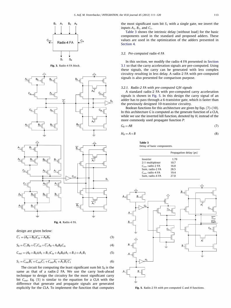
To optimize the speed, we joined two FAs in a single block anduse the carry look-ahead technique [19] to shorten the carry pathwithin the radix-4 FA block. The block diagram of the proposedradix-4 FA is shown in Fig. 3 and the transistor schematic isshown in Fig. 4. The total transistor count is 56. Boolean equationsfor the two carry and two sum gates of the carry-accelerated
Fig. 3. Radix-4 FA block.
Fig. 4. Radix-4 FA.
Table 3Delay of basic components.
Propagation delay (ps)
Inverter 1.79
2:1 multiplexer 10.7
Cout, radix-2 FA 16.0
Sum, radix-2 FA 28.5
Cout, radix-4 FA 19.4
Sum, radix-4 FA 27.0
Fig. 5. Radix-2 FA with pre-computed G and H functions.
S. Asif, M. Vesterbacka / INTEGRATION, the VLSI journal 45 (2012) 111–120 113
design are given below:
C1 ¼ ðA0þB0ÞCinþA0B0 ð3Þ
S0 ¼ C1 B0þC1 CinþC1 A0þA0B0Cin ð4Þ
Cout ¼ ðA0þB0ÞðA1þB1ÞCinþA0B0ðA1þB1ÞþA1B1 ð5Þ
S1 ¼ CoutB1þCoutC1þCoutA1þA1 B1 C1 ð6Þ
The circuit for computing the least significant sum bit S0 is thesame as that of a radix-2 FA. We use the carry look-aheadtechnique to design the circuitry for the most significant carrybit Cout. Eq. (5) is similar to the equation for a CLA with thedifference that generate and propagate signals are generatedexplicitly for the CLA. To implement the function that computes
the most significant sum bit S1 with a single gate, we invert theinputs A1, B1, and C1.
Table 3 shows the intrinsic delay (without load) for the basiccomponents used in the standard and proposed adders. Thesevalues are used in the optimization of the adders presented inSection 4.
3.2. Pre-computed radix-4 FA
In this section, we modify the radix-4 FA presented in Section3.1 so that the carry acceleration signals are pre-computed. Usingthese signals, the carry can be generated with less complexcircuitry resulting in less delay. A radix-2 FA with pre-computedsignals is also presented for comparison purpose.
3.2.1. Radix-2 FA with pre-computed G/H signals
A standard radix-2 FA with pre-computed carry accelerationsignals is shown in Fig. 5. In this design the carry signal of anadder has to pass through a 6-transistor gate, which is faster thanthe previously designed 10-transistor circuitry.
Boolean functions for this architecture are given by Eqs. (7)–(10).In this architecture G is computed as the generate function of a CLA,while we use the inverted kill function, denoted by H, instead of themore commonly used propagate function P:
G0 ¼ AB ð7Þ
H0 ¼ AþB ð8Þ
Fig. 7. G/H pre-computation circuit.
S. Asif, M. Vesterbacka / INTEGRATION, the VLSI journal 45 (2012) 111–120114
Cout ¼ CinH0þG0 ð9Þ
S0 ¼ C1 B0þC1 CinþC1 A0þA0B0Cin ð10Þ
3.2.2. Radix-4 FA with pre-computed G/H signals
The proposed radix-4 FA with pre-computed G/H circuitry isshown in Fig. 6. Compared with the previous radix-4 FA designshown in Fig. 4, the circuitry for Cout is modified so that the carryof an adder has to pass through only a 6-transistor gate instead ofan 18-transistor gate. Hence a speed advantage is obtainedcompared to the standard FA.
The Boolean equations for the circuit are as follows:
G¼ A1B1þðA1þB1ÞA0B0 ð11Þ
H¼ ðA1þB1ÞðA0þB0Þ ð12Þ
Cout ¼ CinHþG ð13Þ
Equations for implementation of C1, S0, and S1 are same asgiven in Section 3.
The circuit for carry acceleration signal generation is shown inFig. 7. A low transistor count is obtained by sharing a part of the
Fig. 6. Proposed radix-4 FA with explicit G/H signals.
Fig. 8. Standard 2-bit CLA.
circuit. Note the case when A1 and B1 are low, and A0 and B0 arehigh. In this case, the NMOS net is used to conduct a high voltageresulting in a reduced voltage swing. However, the inverters atthe outputs provide full voltage swing to subsequent circuits. Thecircuit becomes slower by the sharing, but fortunately it does notaffect the critical path. Another drawback is the reduced noisemargin, which may require a full static CMOS gate for low supplyvoltages.
3.3. Radix-4 FA vs. standard 2-bit CLA
A 2-bit standard CLA is implemented for comparison with theradix-4 FAs. Block diagram for this 2-bit CLA is shown in Fig. 8.
The circuit is implemented using complementary CMOS logicstyle and is realized by Eqs. (14)–(18):
Gi ¼ AiBi ð14Þ
Pi ¼ Ai BiþAiBi ð15Þ
Si ¼ Pi CiþPiCi ð16Þ
C1 ¼ G0þP0C0 ð17Þ
Cout ¼ G1þP1G0þP1P0C0 ð18Þ
This 2-bit CLA uses two PG blocks whereas pre-computedradix-4 FA uses only one pre-computation block named as ‘GHBlock’. Moreover, the complexity of Cout circuit is reduced in
Table 4Results for 2-bit CLA and radix-4 FA.
Basic radix-4 FA Pre-computed radix-4 FA 2-Bit CLA
Technology 45 nm CMOS
PMOS width (mm) 0.2
NMOS width (mm) 0.1
Supply voltage (V) 1.1
Propagation delay (ps) 32.1 24.7 26.3
Transistor count 56 64 90
Energy/operation (fJ) 7.18 8.57 15.07
Fig. 9. Standard scheme of RCA.
Fig. 10. Inverter elimination in carry path for radix-2 RCA.
S. Asif, M. Vesterbacka / INTEGRATION, the VLSI journal 45 (2012) 111–120 115
radix-4 FA using the ‘not kill (H)’ instead of commonly used‘propagate (P)’ signal. Table 4 shows that the radix-4 FAs are notonly faster than the 2-bit CLA, but also better in terms of energyand transistor count. Comparing the pre-computed radix-4 FAwith the basic radix-4 FA, the speed advantage of the former iseven larger, but at the cost of slightly higher energy per operationand transistor count. The increased number of transistors willincrease the area of the circuit, but since the different designsprovide the same regularity, the impact on the layout complexityshould be small.
4. Implementation of 32-bit adders with basic FA
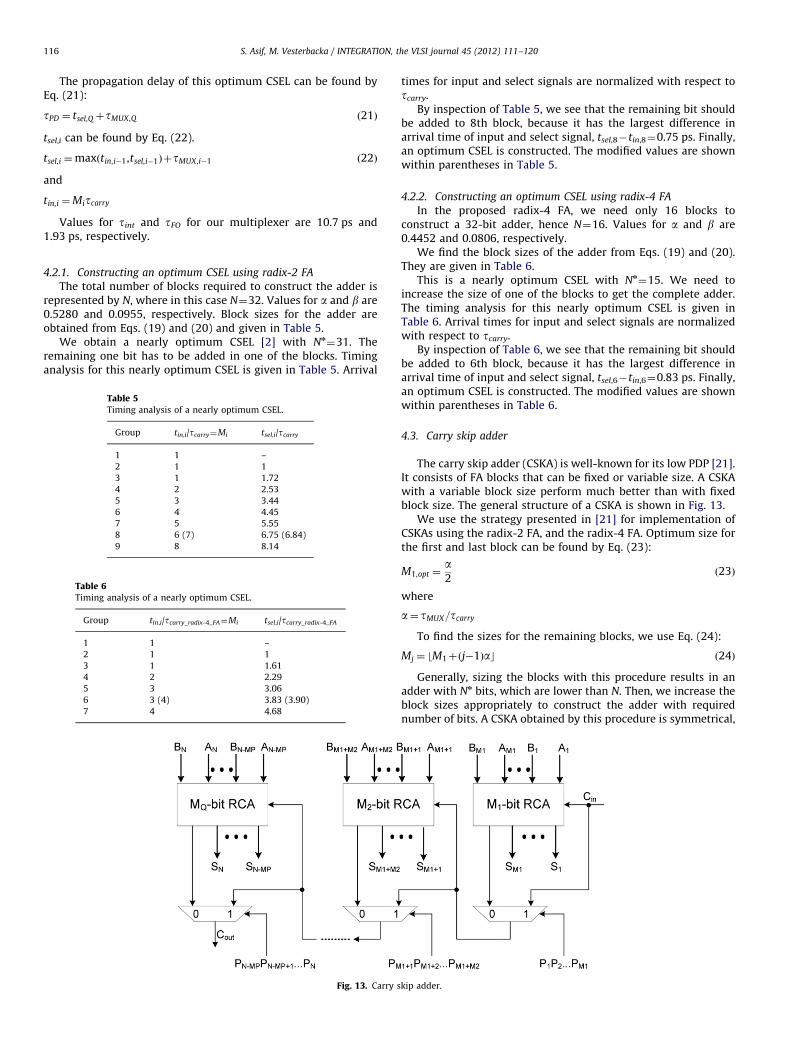
To evaluate the performance of the proposed circuit, we use itto build 32-bit carry propagation adders. Investigated adders arethe ripple carry, carry select, and carry skip adders.
Fig. 11. Inverter elimination in carry path for radix-4 RCA.
4.1. Ripple carry adder
A ripple carry adder (RCA) is used when we have areaconstraints, and when the speed is of little importance [6]. Thestandard scheme of an RCA is shown in Fig. 9.
In order to optimize the RCA delay, we can use the inverterelimination scheme in the carry path [20]. Inverter eliminationschemes for radix-2 and radix-4 RCAs are shown in Figs. 10 and 11,respectively.
With this scheme, the delay and power consumption of theRCA are significantly reduced as compared to when we use thestandard scheme. We used both the standard and the inverterelimination scheme in our experiments, and refer to these in thefollowing as standard scheme and inverter-eliminated scheme,respectively.
Fig. 12. 2-Stage CSA.
4.2. Carry select adder
A carry select adder (CSEL) is commonly used when we need tocompromise between speed and area [2]. A CSEL can be con-structed using constant block size, or a variable block size. Whilethe implementation of constant block size is less complex, thevariable block size gives higher performance than the constantblock size. We implemented both types for comparison purpose.
In the case of constant block size, we implemented a 2-stageCSEL using the radix-4 FA to compare its performance with aradix-2 2-stage CSEL. The block diagram for the 2-stage CSEL isshown in Fig. 12.
We use the strategy presented in [2] to construct a variableblock size CSEL optimized for speed. The size of first and secondblock is computed by Eq. (19):
M1,2 opt ¼aþb
lnð1�bÞð2b�1Þ�aþbb
ð19Þ
where M1,2opt is rounded to nearest integer. In (19),
a¼ tint
tcarryand b¼
tFO
tcarry
where tint is the intrinsic delay of the multiplexer, tFO is increasein multiplexer delay when fan-out is increased by 1, and tcarry isthe carry propagation delay of a FA.
Eq. (20) is used to find the size for the remaining blocks:
Mi ¼M1,2 optþb
Pi�1j ¼ 3 Mjþði�2ÞðaþbÞ
1�b
$ %ð20Þ
for i¼3,yQ, where Q is the total number of blocks in a CSEL.
S. Asif, M. Vesterbacka / INTEGRATION, the VLSI journal 45 (2012) 111–120116
The propagation delay of this optimum CSEL can be found byEq. (21):
tPD ¼ tsel,QþtMUX,Q ð21Þ
tsel,i can be found by Eq. (22).
tsel,i ¼maxðtin,i�1,tsel,i�1ÞþtMUX,i�1 ð22Þ
and
tin,i ¼Mitcarry
Values for tint and tFO for our multiplexer are 10.7 ps and1.93 ps, respectively.
4.2.1. Constructing an optimum CSEL using radix-2 FA
The total number of blocks required to construct the adder isrepresented by N, where in this case N¼32. Values for a and b are0.5280 and 0.0955, respectively. Block sizes for the adder areobtained from Eqs. (19) and (20) and given in Table 5.
We obtain a nearly optimum CSEL [2] with Nn¼31. The
remaining one bit has to be added in one of the blocks. Timinganalysis for this nearly optimum CSEL is given in Table 5. Arrival
Table 5Timing analysis of a nearly optimum CSEL.
Group tin,i/tcarry¼Mi tsel,i/tcarry
1 1 –
2 1 1
3 1 1.72
4 2 2.53
5 3 3.44
6 4 4.45
7 5 5.55
8 6 (7) 6.75 (6.84)
9 8 8.14
Table 6Timing analysis of a nearly optimum CSEL.
Group tin,i/tcarry_radix-4_FA¼Mi tsel,i/tcarry_radix-4_FA
1 1 –
2 1 1
3 1 1.61
4 2 2.29
5 3 3.06
6 3 (4) 3.83 (3.90)
7 4 4.68
Fig. 13. Carry s
times for input and select signals are normalized with respect totcarry.
By inspection of Table 5, we see that the remaining bit shouldbe added to 8th block, because it has the largest difference inarrival time of input and select signal, tsel,8�tin,8¼0.75 ps. Finally,an optimum CSEL is constructed. The modified values are shownwithin parentheses in Table 5.
4.2.2. Constructing an optimum CSEL using radix-4 FA
In the proposed radix-4 FA, we need only 16 blocks toconstruct a 32-bit adder, hence N¼16. Values for a and b are0.4452 and 0.0806, respectively.
We find the block sizes of the adder from Eqs. (19) and (20).They are given in Table 6.
This is a nearly optimum CSEL with Nn¼15. We need to
increase the size of one of the blocks to get the complete adder.The timing analysis for this nearly optimum CSEL is given inTable 6. Arrival times for input and select signals are normalizedwith respect to tcarry.
By inspection of Table 6, we see that the remaining bit shouldbe added to 6th block, because it has the largest difference inarrival time of input and select signal, tsel,6�tin,6¼0.83 ps. Finally,an optimum CSEL is constructed. The modified values are shownwithin parentheses in Table 6.
4.3. Carry skip adder
The carry skip adder (CSKA) is well-known for its low PDP [21].It consists of FA blocks that can be fixed or variable size. A CSKAwith a variable block size perform much better than with fixedblock size. The general structure of a CSKA is shown in Fig. 13.
We use the strategy presented in [21] for implementation ofCSKAs using the radix-2 FA, and the radix-4 FA. Optimum size forthe first and last block can be found by Eq. (23):
M1,opt ¼a2
ð23Þ
where
a¼ tMUX=tcarry
To find the sizes for the remaining blocks, we use Eq. (24):
Mj ¼ bM1þðj�1Þac ð24Þ
Generally, sizing the blocks with this procedure results in anadder with Nn bits, which are lower than N. Then, we increase theblock sizes appropriately to construct the adder with requirednumber of bits. A CSKA obtained by this procedure is symmetrical,
kip adder.
S. Asif, M. Vesterbacka / INTEGRATION, the VLSI journal 45 (2012) 111–120 117
which means it is sufficient to find the block sizes only for left-hand side.
Propagation delay of the designed CSKA can be found by Eq. (25):
tPD ¼ ð2M1�1ÞtcarryþðQ�1ÞtMUXþtsumþDtp,tot ð25Þ
where M1 is the size for first block, Q is the number of total blocks inthe CSKA, tMUX is propagation delay of a multiplexer, tsum is sumpropagation delay of the FA, and Dtp,tot is adder delay increase withrespect to the nearly optimum CSKA when some bits are added to it.
4.3.1. Constructing an optimum CSKA using radix-2 FA
The total number of blocks required to construct the 32-bitadder is N¼32. The value of a is 0.6810. From Eqs. (24) and (25),we find the block sizes M1¼1, M2¼1, M3¼2, M4¼3, M5¼3, andM6¼4. We have to stop at block 6, because adding another blockwill result in a total number of bits for one side greater thanN/2¼16. This is a nearly optimum CSKA with Nn
¼28.Since N�Nn
¼MQ/2, we add another block between the twosides with the same size as that of MQ/2, resulting in a three bitnucleus [21] with M7¼4. Blocks on the right-hand side aresymmetrical to left-hand side with sizes M8¼4, M9¼3, M10¼3,M11¼2, M12¼1, and M13¼1. Thus, our optimum CSKA is completecontaining 13 blocks.
4.3.2. Constructing an optimum CSKA using radix-4 FA
Using the proposed radix-4 FA, we need only N¼16 blocks toconstruct a 32-bit adder. The value of a is 0.5999. The block sizesobtained by Eqs. (23) and (24) are M1¼1, M2¼1, M3¼2, andM4¼2. We have to stop at block, because adding another blockwill result in a total number of bits for one side greater than 8.We obtain a nearly optimum CSKA with Nn
¼12.Since N�Nn4MQ/2, we add another block between the two
sides. The size of this block is determined by Eq. (24), and itrepresents the nucleus [21] with M5¼3. Blocks on the right-handside are symmetrical to the left-hand side with sizes M6¼2,M7¼2, M8¼1, and M9¼1.
We have constructed a nearly optimum CSKA having 30 bitsand now we do need to add one more FA block. These remaining2 bits must be added to the block with the minimum Dtp. Hencewe check for the suitable position to insert the remaining bits tocomplete the 32-bit adder. This limits our search to choose fromM2 and M4, and symmetrically, M8 and M6, respectively. Dtp forthese blocks are
Dtp,2 ¼Dtp,8 ¼ 8:4 ps
Dtp,4 ¼Dtp,6 ¼ 4:2 ps
Dtp,4 and Dtp,6 are lower than Dtp,2 and Dtp,8, so we can addanother FA to either M4 or M6. We add an FA to M4 to completeour optimum CSKA with 9 blocks. The block sizes are M1¼1,M2¼1, M3¼2, M4¼3, M5¼3, M6¼2, M7¼2, M8¼1, and M9¼1.
Table 7Simulation parameters.
Technology 45 nm CMOS
PMOS width (mm) 0.2
NMOS width (mm) 0.1
Supply voltage (V) 1.1
5. Implementation of 32-bit adders with pre-computed FA
The previous set of 32-bit adders has also been implementedwith the pre-computed FAs to evaluate their performance. We usethe same scheme of RCA as described in Section 4.1. However, weneed to re-design the optimized CSEL and CSKA due to the changein delay of the carry signal.
5.1. Constructing an optimum CSEL using radix-2 and radix-4 FA
The new values of a and b for radix-2 FA are 0.5556 and0.1005, respectively. Repeating the procedure described inSection 4.2, we get the group sizes M1¼1, M2¼1, M3¼1, M4¼2,
M5¼3, M6¼4, M7¼5, M8¼7, and M9¼8, which are the same asobtained in Section 4.2.1.
The new values of a and b for the radix-4 FA are 0.6350 and0.1149, respectively. Repeating the procedure described inSection 4.2, we get the group sizes M1¼1, M2¼1, M3¼2, M4¼3,M5¼4, and M6¼5.
5.2. Constructing an optimum CSKA using radix-2 and radix-4 FA
The new value of a for the radix-2 FA is 0.7199. Repeating theprocedure described in Section 4.3, we get the group sizes M1¼1,M2¼1, M3¼2, M4¼3, M5¼3, M6¼4, M7¼4, M8¼4, M9¼3,M10¼3, M11¼2, M12¼1, and M13¼1, which are same as obtainedin Section 4.3.1.
The new value of a for the radix-4 FA is 0.8841. Repeating theprocedure described in Section 4.3, we get the group sizes M1¼1,M2¼2, M3¼2, M4¼3, M5¼3, M6¼2, M7¼2, and M8¼1.
6. Simulation results
6.1. Simulation parameters
In this section we present the simulation results of thedifferent adders that we compare. All the circuits are simulatedin Spice using 45 nm Predictive Technology Model (PTM) formetal gate/high-k [18]. A power supply voltage of 1.1 V is usedfor the simulations. The widths for all NMOS and PMOS transis-tors are set to 0.1 mm and 0.2 mm, respectively. An inverter is usedas load at the outputs for all designs. The simulation parametersare given in Table 7.
For measuring propagation delay we need to set the inputssuch that the carry propagates from LSB to MSB [22]. We setA31�0¼1 and B31�0¼0 to measure the worst-case delay. Then, fortphl we set Cin¼0, and for tplh we set Cin¼1.
Random inputs are applied to the adders to verify the resultsand to estimate the power consumption at fmax for each design.The switching activity of the inputs A and B are 0.23 and 0.26,respectively. A pseudo-random binary sequence generator (PRBS)of Galois type is used to provide the data pattern. The generatorpolynomial for this PRBS is 1þx25
þx26þx30
þx32, which gener-ates a sequence of length 232
�1 [23]. Two different seeds areused for the two PRBS for input A and B. The switching activity ofthe output is 0.23.
For simulation of leakage power, we applied two inputs. Thefirst input is A31�0¼0, B31�0¼0 and Cin¼0, and the second isA31�0¼1, B31�0¼1, and Cin¼1.
6.2. Simulation results for adders with basic FA
Table 8 shows the simulation results for the 32-bit adders withbasic FA. The radix-4 RCA is 1.48 and 1.20 times faster than theradix-2 RCA using standard and inverter eliminated schemes,respectively. The PDP of the radix-4 RCA using standard scheme is19% lower than the radix-2 RCA, but when we compare the RCAsusing inverter eliminated scheme, the radix-4 RCA has 17% higherPDP as compared to the radix-2 RCA. This is because the delay of
Table 8Results for 32-bit adders with basic FA.
Radix Delay
(ps)
Device
count
Power
(mW)
PDP
(fJ)
EDP
(zJ/Hz)
Standard RCA 2 480 768 226 108 52.0
4 324 896 272 88 28.5
Inv. elim. RCA 2 467 736 169 79 36.8
4 389 928 236 92 35.8
2-Stage CSEL 2 285 1356 567 162 46.1
4 207 1536 686 142 29.4
Var. size CSEL 2 173 1980 1129 195 33.8
4 153 2168 1144 175 26.8
Var. size CSKA 2 162 1372 817 132 21.4
4 130 1452 890 116 15.0
Fig. 14. PDP of radix-2 and radix-4 designs with (a) basic FA and (b) pre-
computed FA.
Fig. 15. EDP of radix-2 and radix-4 designs with (a) basic FA and (b) pre-
computed FA.
S. Asif, M. Vesterbacka / INTEGRATION, the VLSI journal 45 (2012) 111–120118
the radix-4 RCA increases due to the domination of parasiticcapacitances. Comparing EDP, standard RCA yields 45% lower EDPfor the radix-4 RCA compared to the radix-2 RCA, and invertereliminated RCA yields 3% lower EDP for the corresponding case.
The radix-4 RCA with the best PDP and EDP values isimplemented with standard scheme, while the radix-2 RCA withthe best PDP and EDP values is implemented with invertereliminated scheme. Comparing these designs, the radix-4 RCAwith standard scheme has a PDP that is 11% higher and an EDPthat is 22% lower than the radix-2 RCA with inverter eliminatedscheme.
A comparison of the 2-stage CSEL adders shows that the radix-4 CSEL is 1.38 times faster, has 12% lower PDP, and 36% lower EDPcompared to the radix-2 CSEL. Similarly, the radix-4 variable sizeCSEL is 1.13 times faster with 10% lower PDP and 21% lower EDPthan the radix-2 variable size CSEL.
Similarly the radix-4 CSKA is 1.25 times faster, has a PDP 12%less, and an EDP 45% less than the radix-2 CSKA.
For the 32-bit adders with basic FA, Fig. 14(a) shows the PDP ofthe radix-2 and radix-4 architectures, Fig. 15(a) shows the EDP ofthe radix-2 and radix-4 architectures, and Fig. 16(a) shows thepower dissipation due to leakage.
The leakage power of the different adders with basic FA isplotted in the graph shown in Fig. 16(a). Comparing leakagepower, the radix-2 RCA implemented with inverter eliminationscheme has the lowest leakage, followed by the radix-4 RCAimplemented with standard scheme, which has 12% higherleakage power dissipation than the radix-2 RCA architectureusing inverter elimination scheme.
The leakage power of the radix-4 2-stage CSEL is 8% higherthan radix-2 2-stage CSEL. Similarly the radix-4 variable size CSELhas 3% higher leakage power dissipation as compared to radix-2variable size CSEL.
The leakage power of the variable size CSKA is approximatelythe same for both the radix-4 and radix-2 designs.
6.3. Simulation results for adders with pre-computed FA
Table 9 shows the simulation results for the 32-bit adders withpre-computed FA. The radix-4 RCA is 2.01 and 1.90 times fasterthan the radix-2 RCA using standard and inverter-eliminatedschemes, respectively. Similarly, the PDP of the radix-4 RCA is26% and 8% lower than the radix-2 RCA, and the EDP is 63% and51% lower than the radix-2 RCA, using standard and inverter-eliminated schemes, respectively.
A comparison of the 2-stage CSEL shows that the radix-4 CSELis 1.75 times faster, has 17% lower PDP, and 53% lower EDP
Fig. 16. Average leakage power of radix-2 and radix-4 designs with (a) basic FA
and (b) pre-computed FA.
Table 9Results for 32-bit adders with pre-computed FA.
Radix Delay
(ps)
Device
count
Power
(mW)
PDP (fJ) EDP
(zJ/Hz)
Standard RCA 2 451 1024 292 132 59.3
4 224 1024 435 98 21.8
Inv. elim. RCA 2 414 992 253 105 43.4
4 218 1056 444 97 21.1
2-Stage CSEL 2 271 1740 736 199 54.0
4 155 1740 1060 164 25.5
Var. size CSEL 2 171 2496 1451 249 42.4
4 135 2404 1611 218 29.4
Var. size CSKA 2 161 1628 975 157 25.3
4 112 1568 1143 128 14.3
S. Asif, M. Vesterbacka / INTEGRATION, the VLSI journal 45 (2012) 111–120 119
compared to the radix-2 CSEL. Similarly, the radix-4 variable sizeCSEL is 1.27 times faster with 13% lower PDP and 31% lower EDPthan the radix-2 variable size CSEL. Comparing the CSEL adders,we see that the variable size CSEL has higher PDP and EDP valuesthan the 2-stage CSEL adders.
Similarly the radix-4 CSKA is 1.44 times faster as compared tothe radix-2 CSKA. The radix-4 CSKA also has 18% lower PDP, and43% lower EDP as compared to radix-2 CSKA.
For the adders with pre-computed FA, Fig. 14(b) shows thecomparison of PDP of the radix-2 and radix-4 architectures,Fig. 15(b) shows the comparison of EDP of the radix-2 andradix-4 architectures, and Fig. 16(b) shows the comparison ofpower dissipation due to leakage.
The leakage power of the different adders with pre-computedFA is plotted in the graph shown in Fig. 16(b). Comparing theleakage power, the radix-4 RCA implemented with standardscheme has the best performance, which is 14% lower than theradix-2 RCA implemented with inverter-eliminated scheme.
The leakage power of radix-4 2-stage CSEL is 13% lower thanthe radix-2 2-stage CSEL. Similarly, the radix-4 variable size CSELhas 15% lower leakage power dissipation as compared to theradix-2 variable size CSEL.
The leakage power of the radix-4 CSKA is 15% lower ascompared to the radix-2 CSKA.
7. Conclusion
In this work, we propose a method of reducing the power-delay and energy-delay products of an adder by reducing thecarry propagation. The method is based on the carry look-aheadtechnique, where we compute the carry without waiting for thecarry out of the previous stage. We implement a radix-4 FA blockby joining two FAs. Within this adder we used the carry look-ahead technique to compute the results for the second sum bit,and thus avoiding carry propagation. The disadvantage of thistechnique is a slightly larger transistor count. A standard 2-bitCLA is also implemented to show the performance improvementof radix-4 adder over 2-bit CLA in terms of speed and powerdissipation. Simulation results show that the proposed radix-4adder has lower energy dissipation per operation as compared to2-bit CLA.
For estimating the performance, we simulate the designs inSpice using a 45 nm technology with a power supply of 1.1 V. Acomparison of adders with a basic FA type shows that the radix-4RCA, 2-stage CSEL, variable size CSEL, and CSKA have a relativePDP of þ11%, �12%, �10%, and �12%, and a relative EDP of�22%, �36%, �21%, and �30% compared to radix-2 RCA, 2-stageCSEL, variable size CSEL, and CSKA, respectively. When comparingadders with a pre-computed FA type, the radix-4 RCA, 2-stageCSEL, variable size CSEL, and CSKA have �8%, �17%, �13%, and�18% relative PDP and �51%, �53%, �31%, and �43% relativeEDP compared to radix-2 RCA, 2-stage CSEL, variable size CSEL,and CSKA, respectively.
Based on these results, we conclude that our proposed radix-4FA gives better performance than a standard radix-2 FA.
A comparison of the two designs of radix-4 adders shows thatthe PDP is �10%, �16%, �24%, and �11%, and the EDP is þ26%,þ13%, �10%, and þ5% for the radix-4 RCA, 2-stage CSEL, variablesize CSEL, and CSKA adders with basic FA relative to the adderswith pre-computed FA, respectively. Hence we can conclude thatthe radix-4 adders with basic FA is better than the adders withpre-computed FA in terms of PDP, but in terms of EDP the radix-4adders with pre-computed FA has better performance on average.
References
[1] A. Neve, H. Schettler, T. Ludwig, D. Flandre, Power-delay product minimiza-tion in high-performance 64-bit carry-select adders, IEEE Transactions onVery Large Scale Integration (VLSI) Systems 12 (3) (March 2004) 235–244.
[2] M. Alioto, G. Palumbo, M. Poli, A gate-level strategy to design carry selectadders, in: Proceedings of the International Symposium on Circuits andSystems, vol. 2, May 2004, pp. 465–468.
[3] J.M. Rabaey, A. Chandrakasan, B. Nikolic, Digital Integrated Circuits: A DesignPerspective, 2nd Edn., Prentice-Hall, 2003.
[5] Yan Sun, Xin Zhang, Xi Jin, High-performance carry select adder using fast all-one finding logic, in: Proceedings of the Second Asia International Conferenceon Modeling and Simulation, May 2008, pp. 1012–1014.
[6] B. Amelifard, F. Fallah, M. Pedram, Closing the gap between carry select adderand ripple carry adder: a new class of low-power high-performance adders,in: Proceedings of the Sixth International Symposium on Quality ElectronicDesign, March 2005, pp. 148–152.
[7] Sun Yan, Zhang Xin, Jin Xi, Low-power carry select adder using fast all-onefinding logic, in: IEEE International Conference on System of SystemsEngineering, 2008, pp. 1–5.
S. Asif, M. Vesterbacka / INTEGRATION, the VLSI journal 45 (2012) 111–120120
[8] R. Shalem, E. John, L.K. John, A novel low power energy recovery full addercell, in: Proceedings of the Ninth Great Lakes Symposium on VLSI, March1999, pp. 380–383.
[9] A. Shams, M. Bayoumi, A novel high-performance CMOS 1-bit full-adder cell,IEEE Transactions on Circuits and Systems II 47 (May 2000) 478–481.
[10] J.-F. Lin, Y.-T. Hwang, M.-H. Sheu, C.-C. Ho, A novel high-speed and energyefficient 10-transistor full adder design, IEEE Transactions on Circuits andSystems I: Regular Papers 54 (5) (2007) 1050–1059.
[11] I. Hassoune, D. Flandre, I. O’Connor, J.-D. Legat, ULPFA: a new efficient designof a power-aware full adder, IEEE Transactions on Circuits and Systems I:Regular Papers 57 (8) (2010) 2066–2074.
[12] M. Alioto, G. Palumbo, Analysis and comparison on full adder block insubmicron technology, IEEE Transactions on Very Large Scale Integration(VLSI) Systems 10 (6) (December 2002) 806–823.
[13] Frank K. Gurkaynad, Yusuf Leblebicit, Laurent Chaouatt, Patrik J. McGuinnessz,Higher radix Kogge–Stone parallel prefix adder architectures, in: Proceedings ofthe ISCAS, 2000.
[14] R. Zlatanovici, B. Nikolic, Power—performance optimal 64-bit carry-looka-head adders, in: Proceedings of the 29th European Solid-State CircuitsConference, ESSCIRC ’03, 2003.
[15] M. Alioto, L. Pancioni, S. Rocchi, V. Vignoli, Power-delay-area-noise margintradeoffs in positive-feedback MOS current-mode logic, IEEE Transactions onCircuits and Systems I: Regular Papers 54 (9) (September 2007) 1916–1928.
[16] M. Anis, M. Allam, M. Elmasry, Impact of technology scaling on CMOS logicstyles, IEEE Transactions on Circuit Systems II: Analog Digital Signal Proces-sing 49 (8) (August 2002) 577–588.
[17] S.M.Y. Sherazi, S. Asif, E. Backenius, M. Vesterbacka, Reduction of substratenoise in sub clock frequency range, IEEE Transactions on Circuits and SystemsI: Regular Papers 57 (6) (June 2010) 1287–1297.
[18] Berkeley Predictive Technology Models (BPTM), 2008. Available from:/http://www.eas.asu.edu/�ptm/S.
[19] M.A. Manzoul, Parallel CLA algorithm for fast addition, in: Proceedings of theInternational Conference on Parallel Computing in Electrical Engineering,2000, pp. 55–58.
[20] Youngjoon Kim, Lee-Sup Kim, A low power carry select adder with reducedarea, in: Proceedings of the IEEE International Symposium on Circuits andSystems, vol. 4, May 2001, pp. 218–221.
[21] M. Alioto, G. Palumbo, A simple strategy for optimized design of one-levelcarry-skip adders, IEEE Transactions on Circuits and Systems. I: FundamentalTheory and Applications 50 (1) (January 2003) 141–148.
[22] K. Rawat, T. Darwish, M. Bayoumi, A low power and reduced area carry selectadder, in: Proceedings of the 45th Midwest Symposium on Circuits andSystems, vol. 1, August 2002, pp. 467–470.
[23] R. Ward, T. Molteno, Table of Linear Feedback Shift Registers, Datasheet,Department of Physics, University of Otago, Dunedin, New Zealand, 2007.
Shahzad Asif received the Bachelors degree in com-puter engineering from COMSATS Institute of Informa-tion Technology (CIIT), Islamabad, Pakistan, in 2005,and the Masters degree in system-on-chip fromLinkoping University, Linkoping, Sweden, in 2008.After his B.Sc. he worked as a Research Associate withCIIT, Islamabad, Pakistan, for two years. He thenreceived a scholarship from (HEC Higher EducationCommission), Pakistan, for his Masters Studies inSweden. Since September 2008, he has been a Lecturerwith CIIT, Islamabad, Pakistan. His research interestsinclude low power circuit design, processor architec-
tures, and FPGA.
Mark Vesterbacka received the M.Sc. degree inapplied physics and electrical engineering, the Lic.Eng. degree in applied electronics, and the Ph.D. degreein electronics systems from Linkoping University,Sweden, in 1991, 1995, and 1997, respectively. From1998 he was an associate professor at LinkopingUniversity where he was appointed a full professor ofelectronics systems in 2002. His research interests arein integrated circuit and system design for commu-nications applications. He is the author and coauthorof more than 90 international and national conferenceand journal publications on digital and mixed-signal
integrated circuits, and he has been granted two patents on data converters.