Page 1
ISSN (Online) 2321 – 2004 ISSN (Print) 2321 – 5526
INTERNATIONAL JOURNAL OF INNOVATIVE RESEARCH IN ELECTRICAL, ELECTRONICS, INSTRUMENTATION AND CONTROL ENGINEERING Vol. 2, Issue 7, July 2014
Copyright to IJIREEICE www.ijireeice.com 1711
Performance Evaluation & Simulation of Solar
Power System
Supreeth K1, K Shanmukha Sundar
2, D.Balamurugan
3
PG Student [Power Electronics], Dept. of EEE, Dayananda Sagar College of Engineering, Bangalore, India 1
Professor & Head, Dept. of EEE, Dayananda Sagar College of Engineering, Bangalore, India 2
DGM-Product Engineering, Tata Power Solar Systems Ltd., Bangalore, India3
Abstract: Major challenges faced in implementing solar photovoltaic electric power generation are high initial cost,
low conversion efficiency of solar modules & unpredictability of solar insolation fluctuations. Before erecting a PV
plant of any capacity in any location, it is best to evaluate the performance of the plant for over a period of time well
before the plant is actually installed. This can be accomplished with help of computer simulation. In this work, the
performance of a 1.155kW solar pv roof top plant has been evaluated by creating a simulation model using MATLAB-
SIMULINK. Simulation model is evaluated for different days’ insolation values without MPPT & with buck-boost
converter & cuk converter, with distributed MPPT. Shadow analysis has been performed on the same module & its
performance for different shading conditions. Simulation outputs for different days’ data were compared with the
practical outputs of the plant & were found to match accurately.
Keywords: Solar Photovoltaics, Photovoltaic (PV), Solar Insolation, Maximum Power Point Tracking (MPPT), Voltage Ripple
I. INTRODUCTION
The demand for electrical energy is increasing year by
year & conversely, our non-renewable energy sources
(coal & oil) are depleting at a much faster rate. In addition
to these two major problems, the amount of environmental
pollution caused while generating power using these
conventional resources has reached the critical stage & its
effects on various life forms including us have been
increasingly noticed all over the globe.
Because of all these reasons, interest & research in utilisation of renewable energy sources has increased at a
large scale globally since the past decade. At the present
situation, among all the known & existing renewable
energy sources, solar & wind energies are the most
promising & reliable energy for large scale electric power
generation. Though using wind energy for electric power
generation is efficient, harvesting solar energy for
electricity generation has been proved to rule out wind
energy based on many number of factors.
Because of all the above facts, India must concentrate on
renewable sources of energy to cope up with the
increasing power demands & environmental hazards. Among the various renewable energy resources, India
possesses a very large solar energy potential. There are
about 300 clear sunny days in a year in most parts of
country. The solar radiation received over the Indian land
area is estimated as five thousand trillion kWh/year. [1]
Long-term research studies on PV solar energy
applications in India started in July 1998, with the testing
of a
1.2 KWp standalone PV system with battery storage, used
for lighting purposes. [2]
PV arrays are used in many applications such as battery chargers, solar powered water pumping systems, grid
connected PV systems, solar hybrid vehicles, & satellite
power systems. In all solar power systems, efficient
simulations including PV panel are required before any
experimental verification. [3]
A major challenge in using a PV source is to tackle its
nonlinear output characteristics. It is very important to
understand & predict the PV characteristics in order to use
a PV installation effectively. [4] The electronics-based modeling of a PV solar cell/module can be realized in
electric/electronic circuits-based simulation softwares. The
electronic components-based models of solar
cells/modules are easy to interface with the power stage.
[5]
To achieve high step-up & high efficiency, DC/DC
converters are the major consideration in the renewable
power applications due to the low voltage of PV modules.
The purpose of dc-dc converter is to insure the impedance
adaptation between the PV source generation & the load.
There are several different types of dc-dc converters, buck,
boost, buck-boost & Cuk topologies. Higher order dc-dc converters, such as the cuk converter, have a significant
advantage over other inverting topologies since they
enable low voltage ripple on both the input & the output
sides of the converter. [6]
II. DESIGNING SOLAR PV ARRAY IN
MATLAB/SIMULINK
A. Solar PV model without MPPT
The module used in the roof top plant array is model
BP3165, made up of 10 strings, with 12 PV cells in series
in each string making a total of 72 cells. The typical
electrical characteristics of the module are listed in table 1.
Page 2
ISSN (Online) 2321 – 2004 ISSN (Print) 2321 – 5526
INTERNATIONAL JOURNAL OF INNOVATIVE RESEARCH IN ELECTRICAL, ELECTRONICS, INSTRUMENTATION AND CONTROL ENGINEERING Vol. 2, Issue 7, July 2014
Copyright to IJIREEICE www.ijireeice.com 1712
TABLE 1
MODULE RATINGS
Electrical Parameter Value
Rated Power (Pmax) 165W
Warranted minimum Power 160W
Voltage at Pmax (Vmp) 35.2V
Current at Pmax (Imp) 4.7A
Open circuit voltage (Voc) 44.2V
Short circuit current (Isc) 5.1A
To make our simulation model reflect these characteristics, we parameterize the solar cell by short
circuit current & open circuit voltage, under 5 parameter
consideration as listed in table 2.
TABLE 2
CELL RATINGS
Electrical Parameter Value
Short-circuit current, Isc 5.1 A
Open-circuit voltage, Voc 0.62 V
Irradiance used for
measurements, Ir0
1000 W/m2
Quality factor, N 1.5
Series resistance, Rs 0.002 Ω
12 cells parameterized as above are connected in series to
form a string, which is then clubbed into a single block.
Six such string blocks are connected in series to form the solar PV module. And the completed model with a load
resistance of 8.6666 Ω (the ratio of Voc & Isc is chosen) is
shown in Fig.1.
B. Evaluation of Solar PV model without MPPT
The data of solar insolation in W/m2, DC current output,
DC voltage output, & output power of the roof top plant
were taken for thirty days, from 8:00 am to 5:00 pm, at an
interval of 15 minutes between each consecutive readings.
It is to be noted that in this work’s simulation, only the insolation
Fig. 1 1.155 kW Solar PV system model without MPPT
Parameter is considered to be the varying factor with
temperature being fixed at a constant temperature. All
further evaluations were done with the presumption of
clear sky, with no dust & no shadow over the array.
The graph in the Fig. 2 compares the practical output
power with the simulated output power & the variation of
two with the variation in insolation level over the time of the day.
Fig. 2 Comparison of practical & simulation output power
There is a huge difference in the practical & simulated
output power values.To rectify the mismatch & make our
model more accurate, we add MPPT technique to our
model.
III. DESIGNING SOLAR PV ARRAY WITH MPPT
A. Solar PV model with Buck-Boost converter
Fig. 3 Buck-Boost converter
Fig. 3 shows the circuit diagram of a simplest buck-boost
converter. A buck-boost converter is obtained by the
cascade connection of the two basic converters. In steady-state, the output to input voltage conversion ratio is the
product of the conversion ratios of the two converters in
cascade (assuming that switches in both converters have
the same duty ratio): Vo
Vd=
D
1−D .......... (1)
This allows the output voltage to be higher or lower than
the input voltage, based on the duty ratio D.
Operation: When the switch is closed, the input provides
energy to the inductor & the diode is reverse biased. When
the switch is open, the energy stored in the inductor is
transferred to the output. No energy is supplied by the
input during this interval. The output capacitor is chosen
to be large enough to achieve constant output voltage.
B. Design of Buck-Boost converter
The design of the Buck-boost converter is done with the
presumptions of necessary parameters of the power stage,
as follows,
Minimum input voltage, Vinmin = 30.2 V
Maximum input voltage, Vinmax = 38.2 V
Desired output voltage, Vout = 35.2 V
Desired output current, Iout = 4.7 A
R
Waveforms
V+
-
Voltage Sensor
String6String5String4String3String2String1
f(x)=0
Solver
Configuration
PSS
Simulink-PS
Converter
Product2
Product1Product Power Value
Store
Photovoltaic Power
in WattsPSS
PS-Simulink
Converter1
PSS
PS-Simulink
Converter
Irradiance
in W/m^2
Irradiance
Electrical Reference
I+
-
Current Sensor
7
Constant
+-8.6666
Page 3
ISSN (Online) 2321 – 2004 ISSN (Print) 2321 – 5526
INTERNATIONAL JOURNAL OF INNOVATIVE RESEARCH IN ELECTRICAL, ELECTRONICS, INSTRUMENTATION AND CONTROL ENGINEERING Vol. 2, Issue 7, July 2014
Copyright to IJIREEICE www.ijireeice.com 1713
Calculation of Duty ratio: The minimum duty cycle for
buck mode & maximum duty cycle for boost mode have to
be calculated first because, at these duty cycles the
converter will be operating at the extremes of its operating
range. The duty cycle is always positive & less than 1.
Let % η = 95%.
Dbuck = Vout X %η
Vinmax= 0.88 .......... (2)
Dboost = 1 − Vinmin X %η
Vout= 0.19 .......... (3)
Where
Dbuck = minimum duty cycle for buck mode. Dboost = maximum duty cycle for boost mode.
Calculation of Inductor rating: For Buck-boost converter an inductor that
satisfies buck & boost mode conditions must be chosen.
The higher the inductor value, the higher will be the
maximum output current because of the reduced ripple
current. Equations 4 & 5 are solved & the largest result
value among the two should be chosen.
Buck mode:
L > Vout X (Vinmax −Vout )
Kind X FswX Vinmax X Iout= 39.21 µH .......... (4)
Where Fsw = the switching frequency of the converter.
L = Inductor value.
Kind is the estimated coefficient that represents the amount
of inductor ripple current relative to the maximum output current. A good estimation for the inductor ripple current
is 20% to 40% of the output current. i.e. 0.2 < Kind < 0.4.
Let, Kind = 0.3 & Fsw = 50000 Hz.
Boost mode:
L > (Vinmin )^2 X (Vout −Vinmin )
Kind X FswX Iout X (Vout )^2= 52.20µH .......... (5)
Hence, L = 53 µH
Calculation of Maximum switch current: The maximum switch currents for buck & boost
mode are calculated & the greater of the two values is
considered.
Buck mode:
Iswmax = Δ Imax
2+ Iout .......... (6)
Where, Iswmax = maximum switch current.
Δ Imax = maximum ripple current through the inductor.
Δ Imax = Vinmax −Vout X Dbuck
Fsw X L=≅ 1.0 A .......... (7)
Iswmax = 1
2+ 4.7 = 5.2 A
Boost mode:
Iswmax = Δ Imax
2+
Iout
1−Dboost .......... (8)
Δ Imax = VinminX Dboost
Fsw X L .......... (9)
Δ Imax = 30.2 X 0.19
50K X 53u = 2.17 A
Iswmax = 2.17
2+
4.7
1 − 0.19 = 6.887 A
Calculation of Capacitor rating:
For Buck-boost converter a capacitor that
satisfies buck & boost mode conditions must be chosen.
Equations 10 & 12 are solved to calculate the minimum
output capacitance for both buck & boost modes of
operation. The selected capacitor must be larger than the minimum required output capacitance for both buck &
boost modes of operation.
Buck mode:
Coutmin = Kind X Iout
8 X Fsw X Voutripple .......... (10)
Where, Coutmin = minimum output capacitance required.
Fsw = switching frequency of the converter.
Voutripple = desired output voltage ripple.
Iout = desired maximum output current.
Kind = estimated coefficient that represents the amount of
inductor ripple current relative to the maximum output
current.
The Equivalent series resistance (ESR) of the output
capacitor adds ripple, which can be calculated using
equation 22.
ΔVoutesr = ESR X Kind X Iout .......... (11)
Where,
ΔVoutesr = output voltage ripple due to capacitor
ESR.
ESR = equivalent series resistance of the used
output capacitor.
ΔVoutesr = 1 X 0.3 X 4.7 = 1.41
Coutmin = 0.3 X 4.7
8 X 50K X 1.41= 2.5 µF
Boost mode:
Coutmin = Iout X Dboost
Fsw X ΔVout .......... (12)
ΔVoutesr = ESR X Iout
1−Dboost+
Kind X Iout X Vout
2 X Vin ........
(13)
= 6.6242
Coutmin = 4.7 X 0.19
50K X 6.6242= 2.7 µF
Hence, C = 3 µF
C. Maximum Power Point Tracking using Perturb & Observe Algorithm
Maximum power point tracking is the technique of
matching the source’s impedance (i.e. voltage to current
ratio) with the load’s impedance to maximize the efficiency of the PV system to the best possible extent.
Though there are numerous algorithms that are used for
this purpose, we concentrate only on perturb and observe
algorithm due to its simplicity and accurate functioning.
The flowchart depicting the embedded matlab function
code used for MPPT is shown in Fig. 4. The final circuit
model including the MPPT control and the buck-boost
Page 4
ISSN (Online) 2321 – 2004 ISSN (Print) 2321 – 5526
INTERNATIONAL JOURNAL OF INNOVATIVE RESEARCH IN ELECTRICAL, ELECTRONICS, INSTRUMENTATION AND CONTROL ENGINEERING Vol. 2, Issue 7, July 2014
Copyright to IJIREEICE www.ijireeice.com 1714
converter is shown in Fig. 5. The o/p capacitor of the
buck-boost converter is chosen with an ESR of 1Ω as
specified in the design.
D. Evaluation of Solar PV Model with Buck-Boost converter
Using the same previous insolation data, solar PV model
with buck-boost converter was evaluated. The graph in
Fig. 6 shows that the results of the solar PV model with
buck-boost converter are in better match with the practical
power values. Although, the output voltage waveform was
of much oscillating nature and in turn the resultant power
waveform was also of similar oscillation which makes it to
be of poor quality when compared to a steady straight line
waveform of a DC.
In order to minimize all these issues and make the output
of the solar PV array to be of more optimum quality, we substitute the buck-boost converter with a cuk converter
and see if it serves the intention.
Fig. 4 Flow chart of P & O algorithm
In the flow chart Dinit is initial duty ratio. Dmax is
maximum duty ratio. Dmin is minimum duty ratio. DeltaD
is perturbation step size. Vold, Pold & Dold are previous
values of voltage, power & duty ratio. V, P & I are present
values of voltage, power & current. dV,dP are difference
in voltage & Power.
Fig. 5 Solar PV model with MPPT & Buck-boost converter
Fig. 6 Comparison of practical & simulation output (with & without
Buck-Boost converter)
E. Solar PV model with Cuk converter
Fig. 7 Cuk converter
Fig. 7 shows the circuit diagram of a simplest cuk
converter. Like the buck-boost converter, cuk converter
also provides a negative polarity regulated output voltage
with respect to the common terminal of the input voltage.
The capacitor C1 acts as the primary means of storing and
transferring energy from the input to the output. In steady-
state, the output to input voltage conversion ratio of the
converter is same as that for the buck-boost converter.
Operation: When the switch is off, the inductor currents iL1 and iL2 flow through the diode. Capacitor C1 is charged
through the diode by energy from both the input and L1.
Current iL1 decreases, because VC1 is larger than Vd.
Energy stored in L2 feeds the output. Therefor iL2 also
decreases.
When the switch is on, VC1 reverse biases the diode. The
inductor currents iL1 and iL2 flow through the switch. Since
VC1 > Vo, C1 discharges through the switch, transferring
energy to the output and L2. Therefore iL2 increases. The
input feeds energy to L1 causing iL1 to increase.
In a buck converter, energy goes to the load when switch
is closed. In a boost converter, energy goes to the load when switch is open. The advantage of cuk converter is
that the energy is transferred to the load both when the
switch is open as well as when the switch is closed. In
general, buck-boost converter the output is much of pulsed
output current which increases the output voltage ripple.
Whereas in the case of cuk converter the output current is
Page 5
ISSN (Online) 2321 – 2004 ISSN (Print) 2321 – 5526
INTERNATIONAL JOURNAL OF INNOVATIVE RESEARCH IN ELECTRICAL, ELECTRONICS, INSTRUMENTATION AND CONTROL ENGINEERING Vol. 2, Issue 7, July 2014
Copyright to IJIREEICE www.ijireeice.com 1715
more of continuous current apparently reducing the output
voltage ripple of the converter, which is a major
advantage. The type of converter used alters the output of
the solar PV array and we make use of this point to
optimize our solar output.
F. Design of Cuk converter
The design of the Cuk converter is done with the
presumptions of necessary parameters as follows,
Minimum insolation = 100 W
Maximum insolation = 1010 W
Minimum input voltage, Vinmin = 30.2 V
Maximum input voltage, Vinmax = 38.2 V
Desired output voltage, Vout = 35.2 V
Switching frequency, f = 50 kHz
Duty ratio = D
Here, both the minimum and maximum input voltages are considered as the two different cases and for each case the
values for the different components for the converter are
found out and the greater value among the two are chosen
for the component.
Case 1: Vin = 30.2 V, Vout = 35.2 V.
w.k.t, Vo
Vd=
D
1−D= 0.59
L1 = 1−D 2 X R
2 X D X f= 28.5µH .......... (14)
L2 = (1−D) X R
2 X f= 36µH .......... (15)
C1 = D
2 X f X R= 681nF .......... (16)
C2 = 1
8 X f X R= 289nF .......... (17)
Case 2: Vin = 38.2 V, Vout = 35.2 V
D = 0.48
Using the equations from 14 to 17, following values were
obtained.
L1 = 49 µH, L2 = 45 µH, C1 = 554 nF
Fig. 8 Solar PV model with MPPT & Cuk converter
G. Evaluation of Solar PV model with Cuk converter
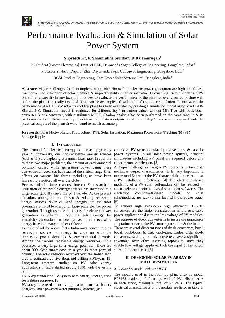
The solar PV array with cuk converter was simulated using the same insolation data and the Fig. 9 shows that
the obtained results are much better than the previous
results. The simulation output with cuk converter was very
much close to the practical output.
Fig. 9 Comparison of practical & simulation output (with & without cuk
converter)
H. Shadow Analysis
Shadow is considered to be an important criteria in PV
systems because, a partial shadow can drastically put
down the output of the system. Shading a single module in
an array will make the entire array to fall down to the level of shaded module and the net impact on the performance
is too high. Now, we will take a PV module and simulate
it with different percentages of shadow and try to evaluate
the module’s performance, which can also reflect the
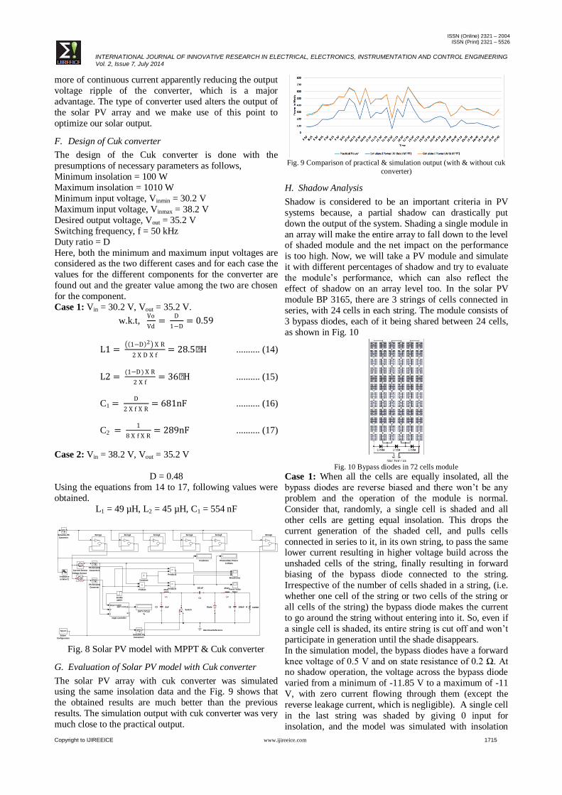
effect of shadow on an array level too. In the solar PV
module BP 3165, there are 3 strings of cells connected in
series, with 24 cells in each string. The module consists of
3 bypass diodes, each of it being shared between 24 cells,
as shown in Fig. 10
Fig. 10 Bypass diodes in 72 cells module
Case 1: When all the cells are equally insolated, all the
bypass diodes are reverse biased and there won’t be any
problem and the operation of the module is normal.
Consider that, randomly, a single cell is shaded and all
other cells are getting equal insolation. This drops the
current generation of the shaded cell, and pulls cells
connected in series to it, in its own string, to pass the same lower current resulting in higher voltage build across the
unshaded cells of the string, finally resulting in forward
biasing of the bypass diode connected to the string.
Irrespective of the number of cells shaded in a string, (i.e.
whether one cell of the string or two cells of the string or
all cells of the string) the bypass diode makes the current
to go around the string without entering into it. So, even if
a single cell is shaded, its entire string is cut off and won’t
participate in generation until the shade disappears.
In the simulation model, the bypass diodes have a forward
knee voltage of 0.5 V and on state resistance of 0.2 Ω. At no shadow operation, the voltage across the bypass diode
varied from a minimum of -11.85 V to a maximum of -11
V, with zero current flowing through them (except the
reverse leakage current, which is negligible). A single cell
in the last string was shaded by giving 0 input for
insolation, and the model was simulated with insolation
49uH49uH681nF
289nF10uF Rmppt enable
V
I
DUTY CYCLE
G
mppt controller
WaveformsV
+-
Voltage Sensor
PS Switch
String6String5String4String3String2String1
f(x)=0
Solver
Configuration
PSS
Simulink-PS
Converter1
PSS
Simulink-PS
Converter
Product2
Product1Product Power Value
Store
Photovoltaic Power
in WattsPSS
PS-Simulink
Converter1
PSS
PS-Simulink
Converter
+ -
L2
+ -
L1
Irradiance
in W/m^2
Irradiance
Enable
MPPT
Electrical Reference
+-
Diode
DUTY CYCLE
%
I+
-
Current Sensor
7
Constant
+-
C3
+-
C2
+ -
C1
+- 8.6666
Page 6
ISSN (Online) 2321 – 2004 ISSN (Print) 2321 – 5526
INTERNATIONAL JOURNAL OF INNOVATIVE RESEARCH IN ELECTRICAL, ELECTRONICS, INSTRUMENTATION AND CONTROL ENGINEERING Vol. 2, Issue 7, July 2014
Copyright to IJIREEICE www.ijireeice.com 1716
data of 1st Feb 2013. The voltage across the bypass diode
connected to the shaded string varied from 0.7 V to 1.03
V, with the module current flowing through it. The graph
in Fig. 11 shows the results.
Fig. 11 Comparison of module output voltage and power without shadow
(Voltage1, Power1) and with a single cell shaded (Voltage2, Power2)
Case 2: The module was shaded longitudinally in terms of
percentage, with a step percentage of 16.66%, which
would cover a 12 cell string with each step, and simulated
with an insolation of 800 W/m2. The fall of the module
voltage, current and power with the increasing shadow
resulted in following graphs in Fig. 12. The graphs show
that, until the very last string is remaining without shadow, we have output. Case 3: When, a minimum of one cell in
all strings of the module is shaded, the output is
zero. This is most likely to happen when there is a
latitudinal shadow over the module, covering a minimum
of one cell in each string. Hence, latitudinal shadow is
more affective on the module’s performance and should be
avoided to the maximum possible extent.
If we consider that in a large array, one or two
modules are shaded as said above, the net current will flow
through the bypass diodes, keeping the loss of power
minimum and avoiding the damage of the system. Keeping all these facts in view, a solar PV array should be
mounted in such a position and angle, such that the
surrounding elements like buildings or poles etc. should
have most minimal chances of creating shadows on the
modules. A mounting angle above 12° helps the modules
to self-clean whenever there is rainfall. In heavily dusted
locations, modules should be cleaned once in a while to
keep the performance of the system at good condition.
Fig. 12 Longitudinal Shadow Analysis
III. SIMULATION RESULTS
The output of the solar PV system here is not a perfect dc. It’s a pulsating (oscillating) dc output with a frequency of
50 kHz (as per the switching frequency of the converter’s
switch). The waveforms of the output current, voltage and
power of the solar PV array with Buck-Boost converter are
as shown in Fig. 13.
Fig. 13 Output Current, Voltage & Power Waveforms of Solar PV array
with Buck-Boost converter
From a random duration of simulation, from 0.1114s to
0.1116, the waveforms are zoomed into. The fig. 5.3
shows that the current level is almost constant at 1.8 A
with no much effective variation. Whereas, the voltage level is much oscillating with a higher difference from a
minima of 227 V to maxima of 242 V. This means that the
variation in voltage level is high and thus the resulting
power waveform is also of similar oscillation which makes
it to be of poor quality when compared to a steady straight
line waveform of a DC. In order to minimize all these
issues and make the output of the solar PV array to be of
more optimum quality, we substituted the buck-boost
converter with a cuk converter and the results were way
better as shown in Fig. 14.
Fig. 14 Output Current, Voltage & Power Waveforms of Solar PV array
with Cuk converter
Page 7
ISSN (Online) 2321 – 2004 ISSN (Print) 2321 – 5526
INTERNATIONAL JOURNAL OF INNOVATIVE RESEARCH IN ELECTRICAL, ELECTRONICS, INSTRUMENTATION AND CONTROL ENGINEERING Vol. 2, Issue 7, July 2014
Copyright to IJIREEICE www.ijireeice.com 1717
As shown in Fig. 14, the output voltage waveform has
much less ripple when compared to that of buck-boost
converter and the shape of the waveform is much
smoother. This is because, a cuk converter is actually the
cascade combination of a boost and a buck converter and
has the advantages of continuous input current and
continuous output current, unlike the case of buck-boost converter which has pulsed input and pulsed output
current. The output power waveform clearly shows that it
is of much higher quality as a DC with a minima of 431 W
and maxima of nearly 433 W. Hence, the oscillation in the
power waveform is very minimal and thus we have
obtained a best converter model for the solar PV array.
The following figures show the difference in current,
voltage and power waveforms of the array with buck-
boost and cuk converters for one day’s insolation data.
Fig. 15 Output waveforms of PV array with buck-boost converter
Fig. 16 Output Waveforms of PV array with Cuk converter
Since model with cuk converter was found to be better,
this model was evaluated with insolation data of 30 days
to check the accuracy of the model and the obtained
results were accurately in match with the practical results.
IV. CONCLUSION
The results of the simulation are much accurate and the
designed model can be used to forecast and predict the output of the array with the availability of insolation data.
By comparing the simulation output with the practical
output, it will be much easier to detect any under
performance and the error/problem can be easily rectified.
The main advantage of this model is that, it can be used to
evaluate the performance over a period of day, or a week
or even a month if we know the insolation data for that
period. It is very convenient to estimate the generation of
the array for longer terms of time. The model can also be
used for the design and estimation of new solar PV arrays
to be built and by changing the cell parameters, any
company’s particular model of module can be realized and
the performance can be evaluated. By performing the
shadow analysis, the performance of the module under shaded conditions can be evaluated and if there are
chances of occurrence of shadow over the array in the
given location, a different module with higher number of
bypass diodes or a module with higher capacity can be
chosen. Both the solar PV model and the converter models
presented are proven to give most accurate results.
ACKNOWLEDGMENT
Thanks to Dayananda Sagar College of Engineering,
Bangalore & Tata Power Solar Systems Ltd., Bangalore
for the infrastructure & support. A special thanks to D.
Balamurugan, DGM-Product Engineering, Tata Power Solar Systems Ltd., & Dr. K. Shanmukha Sundar, HOD,
Dept. of EEE, DSCE for their valuable guidance &
support.
REFERENCES [1] P. Garg, “Energy Scenario and Vision 2020 in India”, Journal of
Sustainable Energy & Environment 3 (2012) 7-17.
[2] S. M. Ali, Arjyadhara Pradhan, “RECENT DEVELOPMENT OF
SOLAR PHOTOVOLTAIC TECHNOLOGIES IN INDIA”,
International Journal of Advances in Engineering & Technology,
May 2012. ISSN: 2231-1963, Vol. 3, Issue 2, pp. 626-634.
[3] Mohamed Azab, “Improved Circuit Model of Photovoltaic Array”,
International Journal of Electrical Power and Energy Systems
Engineering 2:3 2009.
[4] Hiren Patel and Vivek Agarwal, “MATLAB-Based Modeling to
Study the Effects of Partial Shading on PV Array Characteristics”,
IEEE TRANSACTIONS ON ENERGY CONVERSION, VOL. 23,
NO. 1, MARCH 2008.
[5] Yuncong Jiang, Jaber A. Abu Qahouq, Mohamed Orabi,
“Matlab/Pspice Hybrid Simulation Modeling of Solar PV
Cell/Module”, IEEE 978-1-4244-8085-2/11, 2011.
[6] K.Kavitha, Dr. Ebenezer Jeyakumar, “A Synchronous Cuk
Converter Based Photovoltaic Energy System Design and
Simulation”, International Journal of Scientific and Research
Publications, Volume 2, Issue 10, October 2012.
[7] http://en.wikipedia.org/wiki/Sun
[8] http://pveducation.org/pvcdrom/properties-of-sunlight/the-sun
[9] Planning and Installing “Photovoltaic Systems”, A guide for
installers, architects and engineers, second edition, Copyright ©
The German Energy Society (Deutsche Gesellshaft fur
Sonnenenergie (DGS LV Berlin BRB), 2008.
[10] Martin A. Green, Keith Emery, Yoshihiro Hishikawa, Wilhelm
Warta and Ewan D. Dunlop, “Solar cell efficiency tables (version
42)”, PROGRESS IN PHOTOVOLTAICS: RESEARCH AND
APPLICATIONS, Prog. Photovolt: Res. Appl. 2013; 21:827–837
published online in Wiley Online Library (wileyonlinelibrary.com).
DOI: 10.1002/pip.2404.
[11] Data Sheet, 165 watt photovoltaic module, BP 3165, bp solar.
[12] Ned mohan, “Power electronics converters, applications and
design”, Copyright © 2006 by John wiley & sons, ISBN: 978-81-
265-1090-0.
[13] Texas Instruments, “Design Calculations for Buck-Boost
Converters”, Application Report SLVA535A – August 2012 –
Revised September 2012.
[14] Chee Wei Tan, Tim C. Green and Carlos A. Hernandez-Aramburo,
“Analysis of Perturb and Observe Maximum Power Point Tracking
Algorithm for Photovoltaic Applications”, 2nd IEEE International
Conference on Power and Energy (PECon 08), December 1-3,
2008, Johor Baharu, Malaysia.
[15] http://www.mathworks.in/matlabcentral/fileexchange/authors/223753