9
1 Performance modeling and advanced technology node devices Saurabh Sinha R&D, ARM Inc, Austin, TX
1
Performance modeling and advanced technology node devices
Saurabh Sinha R&D, ARM Inc, Austin, TX
2
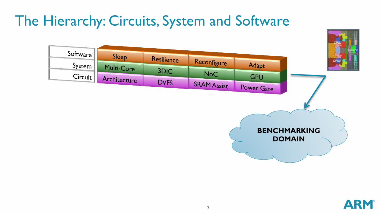
The Hierarchy: Circuits, System and Software
BENCHMARKING DOMAIN
3
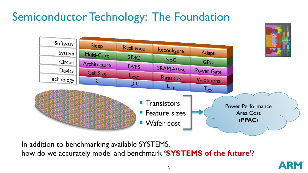
Power Performance Area Cost (PPAC)
Semiconductor Technology: The Foundation
§ Transistors § Feature sizes § Wafer cost
In addition to benchmarking available SYSTEMS, how do we accurately model and benchmark ‘SYSTEMS of the future’?
4
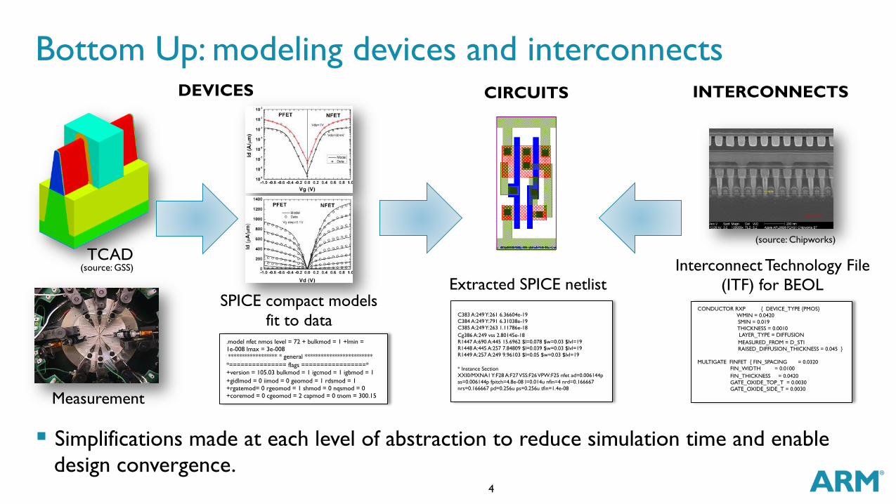
Bottom Up: modeling devices and interconnects
§ Simplifications made at each level of abstraction to reduce simulation time and enable design convergence.
(source: Chipworks)
.model nfet nmos level = 72 + bulkmod = 1 +lmin = 1e-008 lmax = 3e-008 ****************** * general ************************* *=============== flags =================* +version = 105.03 bulkmod = 1 igcmod = 1 igbmod = 1 +gidlmod = 0 iimod = 0 geomod = 1 rdsmod = 1 +rgatemod= 0 rgeomod = 1 shmod = 0 nqsmod = 0 +coremod = 0 cgeomod = 2 capmod = 0 tnom = 300.15
TCAD
Measurement
SPICE compact models fit to data
DEVICES
(source: GSS)
CIRCUITS
C383 A:249 Y:261 6.36604e-19 C384 A:249 Y:791 6.31038e-19 C385 A:249 Y:263 1.11786e-18 Cg386 A:249 vss 2.80145e-18 R1447 A:690 A:445 15.6962 $l=0.078 $w=0.03 $lvl=19 R1448 A:445 A:257 7.84809 $l=0.039 $w=0.03 $lvl=19 R1449 A:257 A:249 9.96103 $l=0.05 $w=0.03 $lvl=19 * Instance Section XXI0/MXNA1 Y:F28 A:F27 VSS:F26 VPW:F25 nfet ad=0.006144p as=0.006144p fpitch=4.8e-08 l=0.014u nfin=4 nrd=0.166667 nrs=0.166667 pd=0.256u ps=0.256u tfin=1.4e-08
Extracted SPICE netlist CONDUCTOR RXP { DEVICE_TYPE {PMOS}
WMIN = 0.0420 SMIN = 0.019 THICKNESS = 0.0010
LAYER_TYPE = DIFFUSION MEASURED_FROM = D_STI RAISED_DIFFUSION_THICKNESS = 0.045 } MULTIGATE FINFET { FIN_SPACING = 0.0320 FIN_WIDTH = 0.0100 FIN_THICKNESS = 0.0420 GATE_OXIDE_TOP_T = 0.0030 GATE_OXIDE_SIDE_T = 0.0030
INTERCONNECTS
Interconnect Technology File (ITF) for BEOL

5
Pushing it up the hierarchy § Logic and SRAM characterized in SPICE and
converted to .LIB format to be used by Synthesis Place & Route tools for block/chip level implementation.
§ Characterization/Implementation at: § Process Corners (TT/FF/SS/Global corners) § Temperatures (-25, 0, 25, 85, 125C) § Voltages (Vnom, Overdrive, Underdrive) § Wire Corners
§ ASSUMPTION: Inaccuracies inherent in converting SPICE to .LIB match one another for logic and SRAM. § How might that change with new devices? Or due to
the inability to voltage scale SRAM?
Source: http://www.opensourceliberty.org
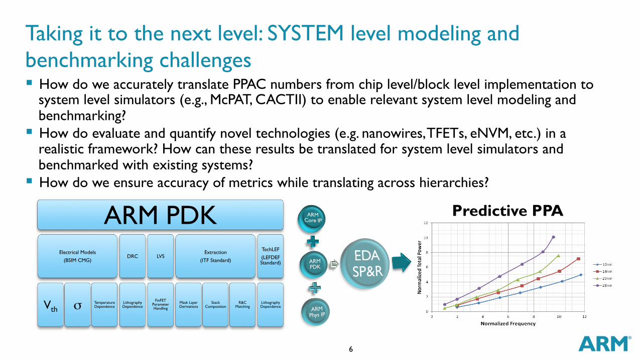
6
Taking it to the next level: SYSTEM level modeling and benchmarking challenges § How do we accurately translate PPAC numbers from chip level/block level implementation to
system level simulators (e.g., McPAT, CACTII) to enable relevant system level modeling and benchmarking?
§ How do evaluate and quantify novel technologies (e.g. nanowires, TFETs, eNVM, etc.) in a realistic framework? How can these results be translated for system level simulators and benchmarked with existing systems?
§ How do we ensure accuracy of metrics while translating across hierarchies?
ARM PDK Electrical Models
(BSIM CMG)
Vth σ Temperature Dependence
DRC
Lithography Dependence
LVS
FinFET Parameter Handling
Extraction
(ITF Standard)
Mask Layer Derivations
Stack Composition
R&C Matching
TechLEF
(LEFDEF Standard)
Lithography Dependence
Predictive PPA
7
FIN Acknowledgements:
Brian Cline Greg Yeric Rob Aitken

8
Backup
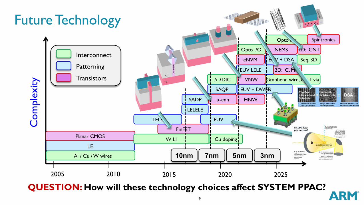
9
LE
Future Technology
2010 2015 2020 2025 2005
Com
plex
ity Transistors
Patterning
Interconnect
FinFET
LELE
SADP
LELELE
EUV
HNW µ-enh
SAQP
// 3DIC Graphene wire, CNT via
EUV LELE
VNW
Opto I/O
EUV + DWEB
2D: C, MoS
EUV + DSA
Opto int Spintronics
Seq. 3D
Al / Cu / W wires
NEMS
Planar CMOS W LI
10nm
eNVM
Cu doping
7nm 5nm 3nm
1D: CNT
QUESTION: How will these technology choices affect SYSTEM PPAC?


