Performance of Partial Reconfiguration in FPGA Systems: A Survey and a Cost Model KYPRIANOS PAPADIMITRIOU, APOSTOLOS DOLLAS Technical University of Crete and SCOTT HAUCK University of Washington Fine-grain reconfigurable devices suffer from the time needed to load the configuration bitstream. Even for small bitstreams in partially reconfigurable FPGAs this time cannot be neglected. In this paper we survey the performance of the factors that contribute to the reconfiguration speed. Then, we study an FPGA-based system architecture and with real experiments we produce a cost model of partial reconfiguration (PR). This model is introduced to calculate the expected reconfiguration time and throughput. In order to develop a realistic model we take into account all the physical components that participate in the reconfiguration process. We analyze the parameters that affect the generality of the model and the adjustments needed per system for error-free evaluation. We verify it with real measurements, and then we employ it to evaluate existing systems presented in previous publications. The percentage error of the cost model when comparing its results with the actual values of those publications varies from 36% to 63%, whereas existing works report differences up to two orders of magnitude. Present work enables a user to evaluate PR and decide whether it is suitable for a certain application prior entering the complex PR design flow. Categories and Subject Descriptors: C.4 [Performance of Systems]: Modeling techniques General Terms: Experimentation, Measurement, Performance, Theory, Verification Additional Key Words and Phrases: Reconfigurable Computing, Field Programmable Gate Ar- rays, Partial Reconfiguration, Reconfiguration Time 1. INTRODUCTION During recent years many applications that exploit the dynamic nature of recon- figurable devices have been developed. Due to their SRAM-based technology, both fine-grain and coarse-grain reconfigurable devices can be reprogrammed potentially unlimited times. This reconfigurability can serve as the vehicle to customize the design of applications even during operation in order to improve their performance Author’s address: K. Papadimitriou and A. Dollas are with the Micropocessor and Hardware Laboratory, ECE Dpt., Technical University of Crete, Kounoupidiana Campus, 73100, Greece. S. Hauck is with the Adaptive Computing Machines and Emulators Laboratory, EE Dpt., University of Washington, Seattle, WA 98195, USA. Part of this work was conducted while K. Papadimitriou was with the University of Washington as a visiting predoctoral student. Permission to make digital/hard copy of all or part of this material without fee for personal or classroom use provided that the copies are not made or distributed for profit or commercial advantage, the ACM copyright/server notice, the title of the publication, and its date appear, and notice is given that copying is by permission of the ACM, Inc. To copy otherwise, to republish, to post on servers, or to redistribute to lists requires prior specific permission and/or a fee. c 20YY ACM 0000-0000/20YY/0000-0001 $5.00 ACM Journal Name, Vol. V, No. N, Month 20YY, Pages 1–0??.
Transcript
Performance of Partial Reconfiguration in FPGASystems: A Survey and a Cost Model
KYPRIANOS PAPADIMITRIOU, APOSTOLOS DOLLAS
Technical University of Crete
and
SCOTT HAUCK
University of Washington
Fine-grain reconfigurable devices suffer from the time needed to load the configuration bitstream.Even for small bitstreams in partially reconfigurable FPGAs this time cannot be neglected. In thispaper we survey the performance of the factors that contribute to the reconfiguration speed. Then,we study an FPGA-based system architecture and with real experiments we produce a cost modelof partial reconfiguration (PR). This model is introduced to calculate the expected reconfigurationtime and throughput. In order to develop a realistic model we take into account all the physicalcomponents that participate in the reconfiguration process. We analyze the parameters that affectthe generality of the model and the adjustments needed per system for error-free evaluation. Weverify it with real measurements, and then we employ it to evaluate existing systems presentedin previous publications. The percentage error of the cost model when comparing its results withthe actual values of those publications varies from 36% to 63%, whereas existing works reportdifferences up to two orders of magnitude. Present work enables a user to evaluate PR and decidewhether it is suitable for a certain application prior entering the complex PR design flow.
Categories and Subject Descriptors: C.4 [Performance of Systems]: Modeling techniques
General Terms: Experimentation, Measurement, Performance, Theory, Verification
Additional Key Words and Phrases: Reconfigurable Computing, Field Programmable Gate Ar-rays, Partial Reconfiguration, Reconfiguration Time
1. INTRODUCTION
During recent years many applications that exploit the dynamic nature of recon-figurable devices have been developed. Due to their SRAM-based technology, bothfine-grain and coarse-grain reconfigurable devices can be reprogrammed potentiallyunlimited times. This reconfigurability can serve as the vehicle to customize thedesign of applications even during operation in order to improve their performance
in terms of different aspects, such as speed, power, and area. In this work we fo-cus on fine-grain partially reconfigurable (PR) devices. Previous published workhas shown that i)specialized circuits can operate at higher speeds vs. their generalstatic counterparts [McKay et al. 1998], ii)chip area is saved by programming onlythe physical resources that are needed in each operation phase [Gholamipour et al.2009], iii)power can be saved by programming only the circuit that is needed, whichallows for static leakage reduction, and by programming optimized circuits, whichallows for dynamic power reduction [Noguera and Kennedy 2007; Paulsson et al.2008].The configuration data produced to program a reconfigurable device is called a
bitstream. When only a portion of a PR device is to be reconfigured a partialbitstream is produced. Although fine-grain devices like FPGAs offer customizationat the bit-level allowing for great flexibility, at the same time they require largebitstreams to be configured as opposed to the coarse-grain devices. This induces aconsiderable reconfiguration time, which cannot be neglected even for devices sup-porting partial reconfiguration. Usually, published reconfiguration times refer to theconfiguration port of the chip only [Lysaght et al. 2006]. There exist works propos-ing the incorporation of PR in their systems, which use such theoretical values anddue to unrealistic assumptions the results are questionable. When incorrectly usedthe reconfiguration time might deviate one or two orders of magnitude from therealistic value [Griese et al. 2004; Galindo et al. 2008]. For “real-world” systems amore holistic approach is needed, taking into account all the system componentsthat contribute to the total reconfiguration overhead, such as the internal and ex-ternal memory, the internal configuration port, the reconfiguration controller, theFPGA configuration memory, and the connections means. As today FPGA plat-forms are used as final products and not just for rapid system prototyping, partialreconfiguration can play a significant role, and thus it would be useful to effectivelyprecalculate its overhead.Performance evaluation frameworks are being developed in order to leverage ex-
isting partial reconfiguration design flows with design space exploration at the earlystages of development [Hsiung et al. 2008]. Our work relies on experiments witha “real-world” platform used as reference, and with straightforward math, we con-struct a model to evaluate reconfiguration time for new platforms without beingnecessary to enter the tedious PR design flow. The model is verified by comparingthe results with real measured data and is used to evaluate previously publishedsystems. Our contributions are:
—a survey with the most recent works on measuring reconfiguration times of PRFPGAs, and an investigation of the performance margins for different systemsetups.
—an analysis of the system factors that contribute to the reconfiguration overheadof which a designer should be aware to evaluate the PR system.
—the formulation of a cost model1 to evaluate reconfiguration in platforms usingan embedded processor to control the reconfiguration; the proposed model does
1available on line in [PRCC 2010].
ACM Journal Name, Vol. V, No. N, Month 20YY.
Performance of Partial Reconfiguration in FPGA Systems: A Survey and a Cost Model · 3
not rely on the throughput of the configuration port alone, and it can be used tocompute the reconfiguration time without performing experiments.
The paper is structured as follows: Section 2 has the basics of partial recon-figuration and discusses recent works that include measurement of reconfigurationtime. In Section 3 we categorize different system setups of published works, and weanalyze the characteristics that affect the performance of reconfiguration. Section4 describes the reference system architecture. Section 5 analyzes the componentsthat contribute to the total reconfiguration time and proposes the cost model. InSection 6 we first verify the model and then use it on different platforms and com-pare its results with real measurements appeared in previous publications of otherresearchers, in order to extract the percentage error. Also we discuss the merits andlimitations of the model. Finally, Section 7 summarizes the benefits of our work.
2. STATE OF THE ART
Several vendors are striving to develop devices supporting partial reconfiguration.Xilinx offers the largest FPGA matrices which incorporate this feature, and mostresearch efforts on this field use devices from this vendor. We focus on these devicesand we provide some background on partial reconfiguration technology along withthe corresponding terminology. Then we discuss recent works that measure the re-configuration time and throughput on “real-world” platforms with modern FPGAs.Some of them include theoretical formulas to calculate the expected results.
2.1 Background on Partial Reconfiguration
The generic structure of the Xilinx Virtex FPGAs is shown in Figure 1. It isa Virtex-II/Pro device [Xilinx Inc. 2007a], one of the most widely used FPGAdevices with partial reconfiguration capability. The newer Virtex-4 and Virtex-5 FPGAs have similar structure. It comprises an embedded processor such as ahardcore PowerPC or a softcore Microblaze, a reconfigurable array, the ProcessorLocal Bus (PLB) [IBM Inc. 2000] and the less efficient On-Chip Peripheral Bus(OPB) [IBM Inc. 2001]. The processor is attached on the PLB bus, which com-municates with the OPB through a bridge. The modules implemented in the arraylogic can be attached to the buses and act as peripherals to the processor. Thearray is 2-D fine-grain heterogeneous, mainly composed of configurable logic blocks(CLBs), hardcore memory blocks (BRAMs), hardcore DSP units (MULTs) and I/Oresources. Each CLB contains look up tables (LUTs), flip-flops, multiplexers andgates that are configured to implement the design logic. The array can be config-ured either externally or internally, by a processor or a dedicated reconfigurationcontroller. The serial JTAG, the SPI and the parallel SelectMAP allow for exter-nal configuration, whereas the parallel Internal Configuration Access Port (ICAP)allows for internal - partial only - configuration. The ICAP in Virtex-II/Pro hasa width of 8-bits, whereas Virtex-4 and Virtex-5 families support 16-bit and 32-bit transfers as well. The maximum operational frequency of ICAP suggested bythe vendor is 100 MHz. A BRAM attached to the ICAP caches the configurationbits before they are loaded to the FPGA configuration memory. An IP core calledOPBHWICAP [Xilinx Inc. 2006] is provided by the vendor which is connected onthe OPB bus as a slave peripheral, and enables a processor to access the configu-
ACM Journal Name, Vol. V, No. N, Month 20YY.
4 · Kyprianos Papadimitriou et al.
ICAP
OP
B
PLB
Fig. 1. The Virtex II-Pro FPGA resources and configuration frames.
ration memory through the ICAP, by using a library and software routines. Forthe Virtex-4 and Virtex-5 FPGAs, the XPSHWICAP [Xilinx Inc. 2007b] has beenreleased, which works similarly with the OPBHWICAP, but it is connected on thePLB bus allowing for lower-latency reconfiguration.
The configuration memory of Virtex-II/Pro is arranged in vertical frames that areone bit wide and stretch from the top edge to the bottom edge of the device. Theyare the smallest addressable segments of the device’s configuration memory space,so all operations must act on entire configuration frames. They do not directlymap to any single piece of hardware; rather, they configure a narrow vertical sliceof many physical resources [Xilinx Inc. 2007a]. A pad frame is added at the endof the configuration data to flush out the pipeline of the reconfiguration processingmachine in order for the last valid frame to be loaded. Therefore, to write evenone frame to the device it is necessary to clock in two frames; the configurationdata frame plus a pad frame. In the newer Virtex devices, the structure and thePR technology is essentially the same, with a few changes. In the previous Virtex-II/Pro family the frame size is not fixed as it is proportional to the entire height ofthe device, which differs amongst the parts. By contrast, in Virtex-4 and -5 familiesthe frame spans a fixed height of the device; its width is one bit. Moreover, the OPBbus is not suggested anymore due to its low performance, and although it will not
ACM Journal Name, Vol. V, No. N, Month 20YY.
Performance of Partial Reconfiguration in FPGA Systems: A Survey and a Cost Model · 5
likely be supported in the future it remains optional within the infrastructure. ThePLBv4.6 (also called XPS) is now the default, which provides more bandwidth, lesslatency and it is more deterministic and stable as compared with the OPB. Also,PLB allows for simultaneous read and write transfers and can be instantiated aseither a shared bus, or for point-to-point connections; the latter option reduces thelatency of transfers between the modules connected on the bus.The PR design flow suggested for complex designs is the module-based flow
[Lysaght et al. 2006]. One or more areas of the FPGA are defined as partiallyreconfigurable regions (PRR). For each PRR more than one module called partiallyreconfigurable modules (PRM), can be created and imported. A partial bitstreamis generated to create each PRM. During operation, the PRMs can be swapped inand out of the corresponding PRR without interrupting the remaining hardware.
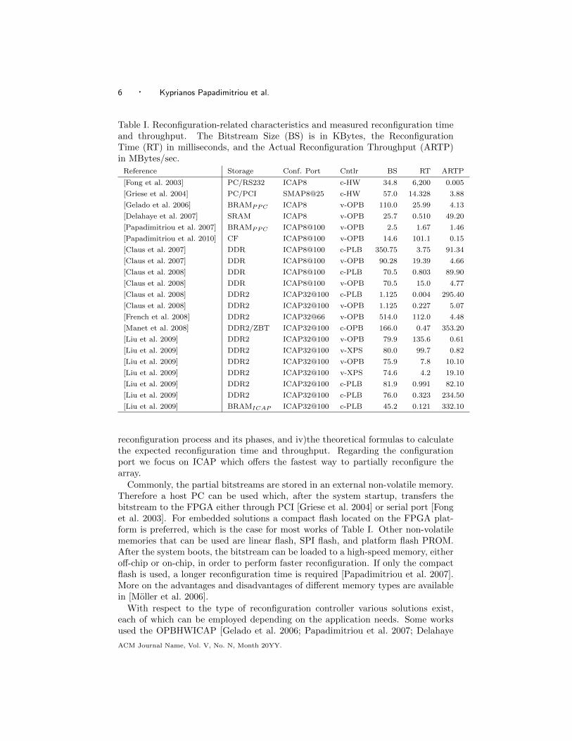
2.2 Reconfiguration Time and Throughput
Table I has some of the most representative works measuring the reconfigurationtime, sorted according to the publication year2. It contains the characteristics of“real-world” platforms, along with the respective reconfiguration time and through-put measured with hardware and/or software means, such as a logic analyzer andsoftware time-stamps. The first column has the Reference. The Storage columnhas the memory means from which the bitstream is loaded to the configurationmemory. The next column consolidates the type, the bit-width and the operationalfrequency in MHz of the Configuration port, e.g. ICAP8@100 refers to the 8-bitICAP port running at 100 MHz. In case a characteristic is missing it means theinformation is not provided by the authors. The column Cntlr refers to the type ofreconfiguration controller. The prefixes “v-” and “c-” define whether the solutionis furnished by the “vendor” or by the authors as a “custom” solution respectively.Thus the c-OPB and the c-PLB refer to a custom reconfiguration controller locatedon the OPB or the PLB bus respectively, whereas the v-OPB and the v-XPS referto the vendor’s OPBHWICAP and XPSHWICAP solutions respectively that arecontrolled by an embedded processor (alternatively a custom core can be imple-mented to interface with the vendor’s OPBHWICAP and XPSHWICAP). The lastthree columns have the Bitstream Size (BS) in KBytes, the corresponding Recon-figuration Time (RT) in msec and the system’s Actual Reconfiguration Throughput(ARTP) in MBytes/sec. The values are included as published, and in the rare case avalue is not explicitly reported in a reference we calculate it, e.g. the fraction of thebitstream size over the reconfiguration time calculates the actual reconfigurationthroughput and vice-versa with the formula ARTP = BS
RT ⇔ RT = BSARTP . All ex-
periments of Table I concern Virtex-II and Virtex-4 FPGAs, mainly the XC2VP30,XC4FX20 and XC4FX60 devices. The 8-bit ICAP corresponds to the Virtex-II,and the 32-bit to the Virtex-4 FPGA families.Along with the Table I, we discuss partially reconfigurable systems by concentrat-
ing on i)the type of the external storage from which the partial bitstream is loadedto the array, ii)the type of the reconfiguration controller, iii)the measurement of the
2At this point we preferred to sort Table I according to the publication year (first column) thanaccording to the reconfiguration throughput (last column). A categorization according to thethroughput is provided in the following Table.
ACM Journal Name, Vol. V, No. N, Month 20YY.
6 · Kyprianos Papadimitriou et al.
Table I. Reconfiguration-related characteristics and measured reconfiguration timeand throughput. The Bitstream Size (BS) is in KBytes, the ReconfigurationTime (RT) in milliseconds, and the Actual Reconfiguration Throughput (ARTP)in MBytes/sec.
Reference Storage Conf. Port Cntlr BS RT ARTP
[Fong et al. 2003] PC/RS232 ICAP8 c-HW 34.8 6,200 0.005
[Griese et al. 2004] PC/PCI SMAP8@25 c-HW 57.0 14.328 3.88
[Gelado et al. 2006] BRAMPPC ICAP8 v-OPB 110.0 25.99 4.13
[Delahaye et al. 2007] SRAM ICAP8 v-OPB 25.7 0.510 49.20
[Papadimitriou et al. 2007] BRAMPPC ICAP8@100 v-OPB 2.5 1.67 1.46
[Papadimitriou et al. 2010] CF ICAP8@100 v-OPB 14.6 101.1 0.15
[Claus et al. 2007] DDR ICAP8@100 c-PLB 350.75 3.75 91.34
[Claus et al. 2007] DDR ICAP8@100 v-OPB 90.28 19.39 4.66
[Claus et al. 2008] DDR ICAP8@100 c-PLB 70.5 0.803 89.90
[Claus et al. 2008] DDR ICAP8@100 v-OPB 70.5 15.0 4.77
[Claus et al. 2008] DDR2 ICAP32@100 c-PLB 1.125 0.004 295.40
[Claus et al. 2008] DDR2 ICAP32@100 v-OPB 1.125 0.227 5.07
[French et al. 2008] DDR2 ICAP32@66 v-OPB 514.0 112.0 4.48
[Manet et al. 2008] DDR2/ZBT ICAP32@100 c-OPB 166.0 0.47 353.20
[Liu et al. 2009] DDR2 ICAP32@100 v-OPB 79.9 135.6 0.61
[Liu et al. 2009] DDR2 ICAP32@100 v-XPS 80.0 99.7 0.82
[Liu et al. 2009] DDR2 ICAP32@100 v-OPB 75.9 7.8 10.10
[Liu et al. 2009] DDR2 ICAP32@100 v-XPS 74.6 4.2 19.10
[Liu et al. 2009] DDR2 ICAP32@100 c-PLB 81.9 0.991 82.10
[Liu et al. 2009] DDR2 ICAP32@100 c-PLB 76.0 0.323 234.50
[Liu et al. 2009] BRAMICAP ICAP32@100 c-PLB 45.2 0.121 332.10
reconfiguration process and its phases, and iv)the theoretical formulas to calculatethe expected reconfiguration time and throughput. Regarding the configurationport we focus on ICAP which offers the fastest way to partially reconfigure thearray.
Commonly, the partial bitstreams are stored in an external non-volatile memory.Therefore a host PC can be used which, after the system startup, transfers thebitstream to the FPGA either through PCI [Griese et al. 2004] or serial port [Fonget al. 2003]. For embedded solutions a compact flash located on the FPGA plat-form is preferred, which is the case for most works of Table I. Other non-volatilememories that can be used are linear flash, SPI flash, and platform flash PROM.After the system boots, the bitstream can be loaded to a high-speed memory, eitheroff-chip or on-chip, in order to perform faster reconfiguration. If only the compactflash is used, a longer reconfiguration time is required [Papadimitriou et al. 2007].More on the advantages and disadvantages of different memory types are availablein [Moller et al. 2006].
With respect to the type of reconfiguration controller various solutions exist,each of which can be employed depending on the application needs. Some worksused the OPBHWICAP [Gelado et al. 2006; Papadimitriou et al. 2007; Delahaye
ACM Journal Name, Vol. V, No. N, Month 20YY.
Performance of Partial Reconfiguration in FPGA Systems: A Survey and a Cost Model · 7
et al. 2007; Claus et al. 2007; Claus et al. 2008; French et al. 2008; Liu et al. 2009]whereas a few experimented with the XPSHWICAP [Liu et al. 2009]. On the otherhand, customized reconfiguration controllers aim to speedup reconfiguration and/orrelease the processor time to other tasks, such as the reconfiguration managementunder the supervision of an operating system [Santambrogio et al. 2008]. This canbe done either through Direct Memory Access (DMA) with a customized controlleron the OPB [Manet et al. 2008] or the PLB bus [Claus et al. 2007; Claus et al. 2008;Liu et al. 2009], or with a PLB master connected directly with the controller of theexternal memory, allowing for burst transmissions [Liu et al. 2009]. Moreover, tospeed up reconfiguration, partial bitstreams can be loaded immediately after thesystem startup into large on-chip memory implemented with BRAMs attached tothe reconfiguration controller [Liu et al. 2009]. In general, the systems with theprocessor acting as the reconfiguration controller suffer from long delays due to thelarge time needed to access its program memory to call and execute the softwareinstructions. Also, when several modules are connected to the bus the delay is longerand unstable due to the contention between reconfiguration and data transfers.
The distinct phases during reconfiguration can vary depending on the systemsetup. The measured times mainly concern the phase to pull the bitstream from theoff-chip memory to the local memory of the processor, copy it from the local memoryof the processor to the ICAP, and send it from the ICAP to the FPGA configurationmemory [Gelado et al. 2006; Papadimitriou et al. 2007; French et al. 2008]. Thesesubtasks iterate until the entire partial bitstream is written to the configurationmemory [Papadimitriou et al. 2010]. For specific systems other subtasks have beenmeasured, such as the time for configuration code analysis to guarantee safety,initialization and start time of the reconfiguration controller [Griese et al. 2004],the time to send the adequate instructions to the ICAP [Gelado et al. 2006], and thetime to copy the configuration data from user space to kernel space in Linux [Frenchet al. 2008]. In all systems the largest overhead comes from the bitstream transferfrom the external memory to the on-chip memory [Griese et al. 2004; Papadimitriouet al. 2007; 2010], and from the processor to the ICAP through the bus [Geladoet al. 2006; French et al. 2008; Delahaye et al. 2007].
Although some of the above works evaluate the time spent in each reconfigurationphase, they do not provide a theoretical analysis taking into account the systemcharacteristics. Some of them calculate the expected reconfiguration throughputbased on the bandwidth of the configuration port only [Claus et al. 2007; Manetet al. 2008]. However, in [Griese et al. 2004] the authors demonstrated that theactual reconfiguration throughput deviates one order of magnitude from the theo-retical bandwidth of the configuration port. In another work this deviation reachesup to two orders of magnitude [Galindo et al. 2008]. Following the same concept,Lysaght et al. [Lysaght et al. 2006] reports the reconfiguration times for Virtex-IIPro and Virtex-4 devices. For example the partial bitstream for 25% of a XC2VP30,which is equal to 353 KBytes, can be loaded in less than 6 ms when the ICAP op-erates at 100 MHz and is fully utilized. This has a considerable difference with theend-to-end system times, and depending on the system setup the actual reconfig-uration times can take significantly longer, as demonstrated in Table I. Claus etal. [Claus et al. 2008] provide a more sophisticated model to calculate the expected
ACM Journal Name, Vol. V, No. N, Month 20YY.
8 · Kyprianos Papadimitriou et al.
reconfiguration throughput and latency. However, this model is based on the char-acteristics of the configuration port itself only; these are the operational frequency,the interface width and the frequency of activation of the ICAP’s “BUSY” hand-shaking signal. This model cannot be safely applied on the Virtex-4 devices dueto the different behavior of the “BUSY” signal in the specific family. Althoughthis model can be fairly accurate under specific circumstances, if a designer wantsto evaluate a system, (s)he would need to built it first, then evaluate it, and thenexamine whether it meets the application needs. We are interested in a modelthat will provide better estimation regardless of the maximum throughput of theconfiguration port early in the design stage.
3. INVESTIGATION OF THE RECONFIGURATION PERFORMANCE
In this Section we analyze further the characteristics that affect the reconfigura-tion performance. Table II categorizes the existing approaches according to theconfiguration port and its bandwidth, the reconfiguration controller and the stor-age means. It also summarizes the expected range of the actual reconfigurationthroughput according to the system characteristics. We observe that the through-put varies heavily depending on the three characteristics.When comparing the cases A and B where the PowerPC (PPC) processor is the
reconfiguration controller, loading the partial bitstream from the local memory ofthe processor implemented with BRAMs offers a speedup of 10x over the compactflash solution [Papadimitriou et al. 2007]. In case I, where on-chip memory im-plemented with BRAMs attached to the ICAP is used to fetch the entire partialbitstream prior reconfiguration takes place, much better results are produced. Inthis case a dedicated reconfiguration controller accounts for the high throughput,as it continuously pulls the prefetched configuration data; this allows for the almostfull utilization of the configuration port [Liu et al. 2009].In case D where a customized reconfiguration controller located on the PLB bus
is utilized, the reconfiguration throughput reaches almost the bandwidth of the8-bit ICAP configuration port [Claus et al. 2007; Claus et al. 2008]. However in
Table II. Comparison between the bandwidth of the configuration port and theactual reconfiguration throughput for different published system setups.
Configuration Port
case Type Bandwidth Cntlr Storage ARTP
A
ICAP8@100 95.3 MB/s
v-OPB CF 0.15 MB/s
B v-OPB BRAMPPC 1.46 MB/s
C v-OPB DDR 4.54-4.77 MB/s
D c-PLB DDR 89.90-91.34 MB/s
E
ICAP32@100 381.5 MB/s
v-OPB DDR2 0.61-11.1 MB/s
F v-XPS DDR2 0.82-22.9 MB/s
G c-OPB DDR2/ZBT 353.2 MB/s
H c-PLB DDR2 82.1-295.4 MB/s
I c-PLB BRAMICAP 332.1-371.4 MB/s
ACM Journal Name, Vol. V, No. N, Month 20YY.
Performance of Partial Reconfiguration in FPGA Systems: A Survey and a Cost Model · 9
case H when the 32-bit ICAP is used, the same setup cannot achieve the configu-ration port bandwidth. This might be due to the DDR2 SDRAM controller whichis not able to feed the reconfiguration controller fast enough in order to attain theICAP bandwidth [Claus et al. 2008; Liu et al. 2009]. High throughput approachingthe theoretical maximum is also achieved in case G with a custom reconfigurationcontroller located on OPB [Manet et al. 2008]. In this work, the authors reportedthat the throughput was ranging from 0.46 to 353.2 MB/sec for different systemsetups depending on the reconfiguration controller and the type of external mem-ory. Their fastest solution was provided with a custom OPB ICAP reconfigurationcontroller when the partial bitstreams were loaded from a high-speed external mem-ory; however the authors do not report whether the DDR2 SDRAM or the ZBTSRAM was used. They were not able to reach the maximum throughput due tothe DMA overhead. Also, due to a clock skew problem they sent the configurationdata on the falling edge of the ICAP clock. It is interesting to notice that thethroughput of the best case of the custom OPB controller of [Manet et al. 2008]which is 353.2 MB/s is higher than the custom PLB controller of [Claus et al. 2008]which is 295.4 MB/s, despite the fact that the former is attached on the OPB busand the latter on the more-efficient PLB bus (see Table I of Section 2). We seetwo possible reasons that the system with the OPB reconfiguration controller offershigher throughput; either i)the bitstreams are fetched from the ZBT SRAM whichprovides higher throughput than the DDR2 SDRAM and consequently allows forhigher utilization of the ICAP bandwidth, or ii)if the bitstreams are fetched fromthe DDR2 SDRAM, the corresponding controller is implemented more efficiently.When the processor acts as the reconfiguration controller its settings can affect
significantly the reconfiguration speed. This holds for both the OPBHWICAP andthe XPSHWICAP of cases E and F respectively. Such settings are the selectionof a hardcore processor (e.g PowerPC), or a softcore processor (e.g. Microblaze),and the incorporation of separate instruction cache and data cache [Liu et al. 2009].Another study shows that the change of the amount of memory allocated in the pro-cessor local memory for buffering reads and write calls to the compact flash causedvariations in the reconfiguration time with respect to the number of reconfigurationframes [Papadimitriou et al. 2010]. Another action towards increase of reconfigura-tion performance is the replacement of the vendor’s Application Program Interface(API) that handles the ICAP accesses with a better one [Moller et al. 2006].Based on the above works we conclude that for recent PR technology on “real-
world” systems:
—The reconfiguration throughput of the system cannot be calculated from thebandwidth of the configuration port alone. To evaluate the system holistically,the overhead added by the components participating in the reconfiguration pro-cess should be taken into account.
—The characteristics that affect the reconfiguration overhead depend on the systemsetup, such as the external memory and the memory controller, the reconfigura-tion controller and its interface with the configuration port, and the user spaceto kernel space copy penalty when an operating system running on the processorcontrols the reconfiguration.
—A bus-based system that connects the processor, the partially reconfigurable mod-
ACM Journal Name, Vol. V, No. N, Month 20YY.
10 · Kyprianos Papadimitriou et al.
ule(s), the static module(s), and the configuration port, can be non-deterministicand unstable due to the contention between data and reconfiguration transfers.
—A large on-chip memory implemented with BRAMs attached to the configurationport that prefetches the bitstreams after the system boots can allow for fastreconfiguration. Due to the limited size of BRAMs in FPGAs, the utilizationcost should be considered according to the application needs, i.e. using BRAMsto prefetch configuration vs. saving BRAMs to deploy the circuits.
—The settings of the processor can affect the reconfiguration time. Moreover, thesize of the local memory of the processor can affect significantly the reconfigu-ration time. However, similar to the above case the cost of BRAM utilizationshould be considered.
—The selection of the reconfiguration controller depends on the application needs,the available resources, the speed and the power constraints. For example, in casearea is of greater concern than speed, and an operating system executes on anembedded processor, the latter can undertake the reconfiguration process in orderto avoid the consumption of logic resources to implement a dedicated reconfig-uration controller. Previous works suggested ways to reduce the reconfigurationoverhead if this is needed [Hauck 1998; Papadimitriou and Dollas 2006].
—Nearly the full bandwidth of the configuration port can be used with a dedi-cated reconfiguration controller that is either equipped with DMA capabilities,or acts as a master directly connected to the configuration port allowing for bursttransmissions. Also, effective design choices at the system level should be madesuch as the usage of a high-speed memory to store the partial bitstreams afterpower-up and an efficient memory controller.
Obviously only the development of an efficient reconfiguration controller can al-low for the actual reconfiguration throughput to approach the ICAP bandwidth.However, this is not the common case either due to the system components thatbound the full utilization of the ICAP or the designer’s choices and applicationneeds. A cost model to precalculate the expected reconfiguration time can assist inthe performance evaluation phase. Moreover, it would be beneficial if this modelcould be used early in the design flow in order to either i)prevent the designer fromentering the tedious PR design flow, or, ii)timely change the settings of the systemsetup. The evaluation can be done either right after the bitstream estimation of thepartially reconfigurable modules at the initial budgeting stage of the floorplanningstage, or even after the synthesis results. Although the latter method is less accu-rate, our experience so far showed that the cost model still produces satisfactoryresults.Several works exploring applications that benefit from partial reconfiguration
can be augmented with a cost model for partial reconfiguration in order to providerealistic data. For the dynamically reconfigurable network processor proposed in[Kachris and Vassiliadis 2006] the cost model can calculate the time needed for re-configuration after which the system will meet the network workload. Bitstreams ofdifferent encoding, encryption and transcoding modules are fairly large and shouldbe located in an external memory, so, the added overhead before the system is readyto execute is useful to know. In the field of multi-mode communication systems the
ACM Journal Name, Vol. V, No. N, Month 20YY.
Performance of Partial Reconfiguration in FPGA Systems: A Survey and a Cost Model · 11
Table III. Size of BRAM resources for moderate-sized FPGAs of Virtex-II,-4,and -5 families. TheTable illustrates the maximum size of the bitstreams that can be prefetched in the extreme casenone of the actual circuits utilizes BRAMs.
FPGA BRAM size (KBytes)
XC2VP30 306
XC4FX60 522
XC5VLX50T 270
cost model can be used to calculate the time to load the optimized configurationsof the filters [Gholamipour et al. 2009].Furthermore, assuming that unlimited amount of on-chip memory is available to
fetch the entire bitstream and then load it at the ICAP’s speed is not realistic. Ananalysis on the memory resources required by the circuit itself when deployed inthe field should be performed firstly by the designer. Also, an analysis of the localmemory of the processor and the bitstream size is needed, prior deriving the amountof BRAMs that can be allocated for bitstream prefetching. Table III shows thatmoderate-size FPGAs commonly used for research have limited BRAM resources.In many cases the amount of on-chip memory imposes limitations to the size ofthe bitstreams that can be prefetched; this is obtained from Table I that containsbitstream sizes for several “real-world” applications.
4. SYSTEM ARCHITECTURE
Initially we present the general architecture of a partially reconfigurable system,and then we describe in detail a realistic system with a Xilinx Virtex-II Pro FPGA.It is used as the reference system to develop the cost model.
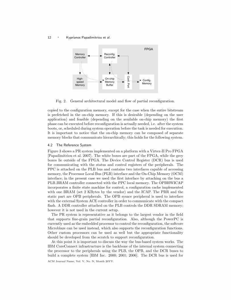
4.1 General Architectural Model
Figure 2 illustrates the general architectural model of a PR FPGA-based system.The FPGA main components are the array, the configuration memory that pro-grams the array, the reconfiguration controller, the configuration port and the on-chip memory buffer. The connection between them is made either point-to-pointor through a bus. Other system components are the volatile high-speed memoryfrom which the partial bitstreams are loaded and its memory controller. The mem-ory controller can reside either off-chip or on-chip implemented as an IP module.Other necessary components are the non-volatile memory used as a repository forthe partial bitstreams and its controller. However, these are omitted from Figure 2as after the system boots, the bitstreams can be copied to the high-speed memory(for faster reconfiguration), and thus they do not need to be involved in the processagain. If the off-chip high-speed memory is left out and each time the bitstream isloaded directly from the compact flash, throughput becomes flash-dominated andlittle transfer speed improvement is possible.The configuration takes place in two distinct phases shown with the dashed lines.
Once the memory controller is instructed to load the bitstream, it is copied from theoff-chip memory to the on-chip memory buffer. Then the reconfiguration controllerloads the bitstream to the FPGA configuration memory through the configurationport. These phases occur alternately in succession until the entire bitstream is
ACM Journal Name, Vol. V, No. N, Month 20YY.
12 · Kyprianos Papadimitriou et al.
Conf. P
ort
Memory
Controller
High-
speed
Memory
On-chip
Memory
Buffer
Reconfig.
Controller
Config.
Memory
Fig. 2. General architectural model and flow of partial reconfiguration.
copied to the configuration memory, except for the case when the entire bitstreamis prefetched in the on-chip memory. If this is desirable (depending on the userapplication) and feasible (depending on the available on-chip memory) the firstphase can be executed before reconfiguration is actually needed, i.e. after the systemboots, or, scheduled during system operation before the task is needed for execution.It is important to notice that the on-chip memory can be composed of separatememory blocks that communicate hierarchically; this holds for the following system.
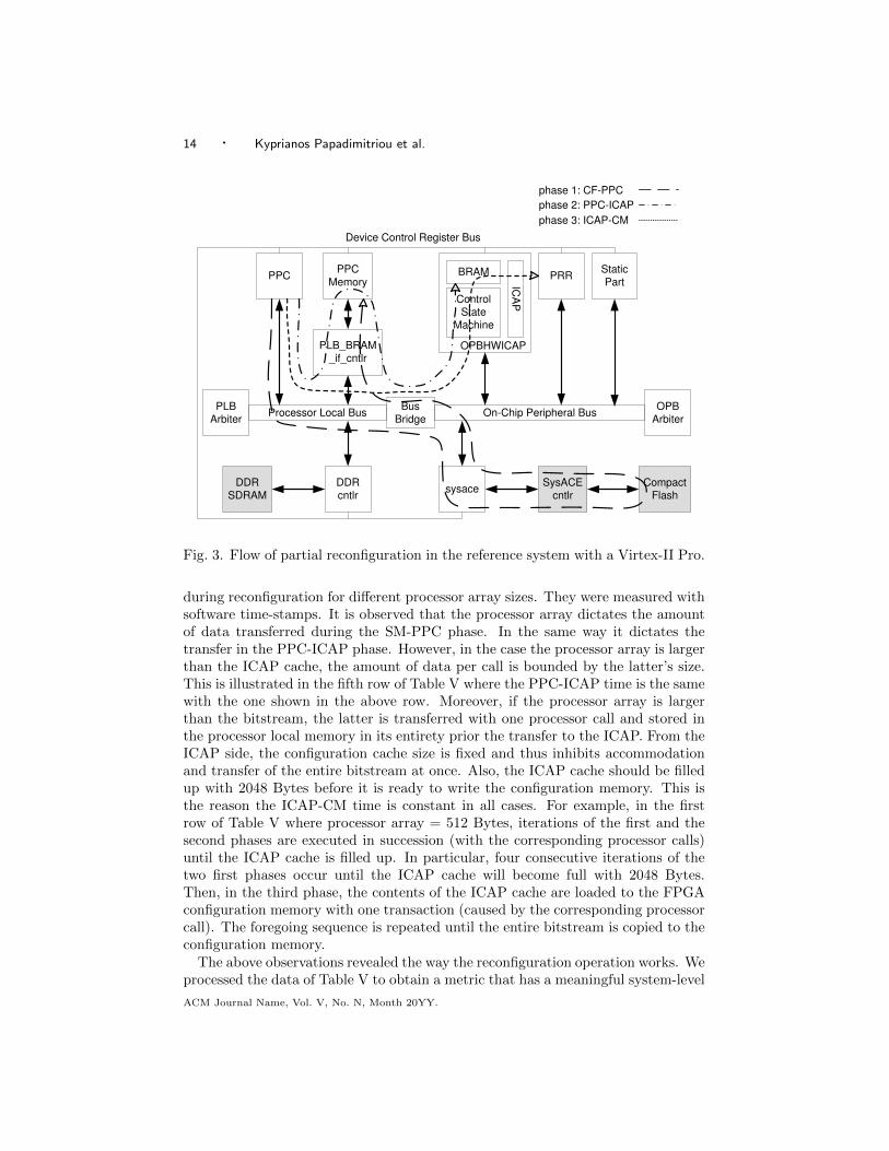
4.2 The Reference System
Figure 3 shows a PR system implemented on a platform with a Virtex-II Pro FPGA[Papadimitriou et al. 2007]. The white boxes are part of the FPGA, while the greyboxes lie outside of the FPGA. The Device Control Register (DCR) bus is usedfor communicating with the status and control registers of the peripherals. ThePPC is attached on the PLB bus and contains two interfaces capable of accessingmemory, the Processor Local Bus (PLB) interface and the On-Chip Memory (OCM)interface; in the present case we used the first interface by attaching on the bus aPLB BRAM controller connected with the PPC local memory. The OPBHWICAPincorporates a finite state machine for control, a configuration cache implementedwith one BRAM (set 2 KBytes by the vendor) and the ICAP. The PRR and thestatic part are OPB peripherals. The OPB sysace peripheral is used to interfacewith the external System ACE controller in order to communicate with the compactflash. A DDR controller attached on the PLB controls the DDR SDRAM memory;however it is not used in the current setup.The PR system is representative as it belongs to the largest vendor in the field
that supports fine-grain partial reconfiguration. Also, although the PowerPC iscurrently used as the embedded processor to control the reconfiguration, the softcoreMicroblaze can be used instead, which also supports the reconfiguration functions.Other custom processors can be used as well but the appropriate functionalityshould be developed from the scratch to support reconfiguration.At this point it is important to discuss the way the bus-based system works. The
IBM CoreConnect infrastructure is the backbone of the internal system connectingthe processor to the peripherals using the PLB, the OPB, and the DCR buses tobuild a complete system [IBM Inc. 2000; 2001; 2006]. The DCR bus is used for
ACM Journal Name, Vol. V, No. N, Month 20YY.
Performance of Partial Reconfiguration in FPGA Systems: A Survey and a Cost Model · 13
Table IV. System settings.
Parameters Size
CF sector 512 Bytes
PLB BRAM block 48 KB
stack 6 KB
buffer cache 0.5-4 KB
processor array 0.5-4 KB
ICAP BRAM cache 2 KB
accessing status and control registers within the PLB and OPB masters and slaves.It off-loads the PLB and the OPB from the lower performance read/write transfersfrom/to the status and control registers. It also decreases access latency duringperiods of high processor bus utilization. DCR is not part of the system memorymap, and thus it removes configuration registers from the memory address map,allowing for data transfers to occur independently from, and concurrent with, PLBand OPB transfers.In the setup of Figure 3, the PPC is the controller of the reconfiguration process
carried out in three distinct phases that are repeated until the entire bitstreamis written in the configuration memory [Papadimitriou et al. 2010]. These phasesare shown with the dashed lines: i)First the PPC requests the bitstream from theexternal storage means (the compact flash in the present case) and writes it inits local memory (first level of the on-chip memory hierarchy) with block-by-blocktransactions, ii)then the PPC transfers the bitstream word-by-word to the ICAPconfiguration cache (second level of the on-chip memory hierarchy), and iii)oncethe configuration cache is full the PPC instructs the OPBHWICAP to load thebitstream to the FPGA configuration memory through the ICAP. These actionsare determined with software commands residing in the PPC program memory.For sake of simplicity we will refer to them as SM-PPC3, PPC-ICAP and ICAP-CM respectively.Table IV has the system parameters we configured as fixed and those we varied
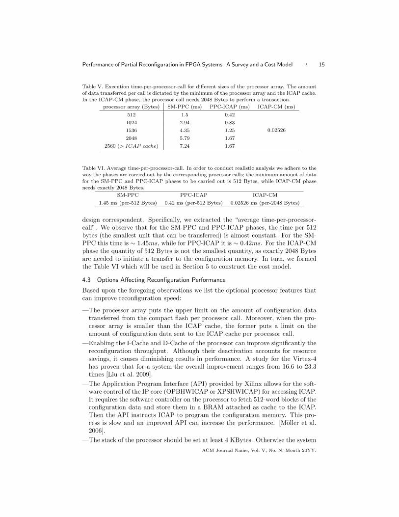
to examine their affect on performance. The PPC’s local memory was 48 KBytesand the stack was 6 KBytes. The buffer cache (bc) defines the amount of memoryfor buffering read and write calls to the System ACE controller. The processorarray (pa) is allocated in the PPC local memory to store the configuration data,and determines the amount of data read from the compact flash per transaction4.The ICAP cache has fixed size set by the vendor one BRAM, which is equal to 2KBytes. In order to configure a system with low resources we did not enable theinstruction/data caches and interrupts of the PPC.Table V has the time spent in the processor calls (which force the transactions)
3SM and CF acronyms are used throughout the paper depending on the type of storage we referto, i.e. SM stands for storage means referring to a general type of memory, either volatile ornon-volatile, high-speed or low-speed, and CF stands for the compact flash which is non-volatilelow speed memory.4Transactions are conducted in multiples of one sector per processor call. A sector is the smallestunit the compact flash is organized in and is equal to 512 Bytes. Thus we varied the processorarray size in multiples of one sector.
ACM Journal Name, Vol. V, No. N, Month 20YY.
14 · Kyprianos Papadimitriou et al.
Processor Local Bus On-Chip Peripheral Bus
BRAM
Control
State
Machine
ICA
P
OPBHWICAP
phase 1: CF-PPC
phase 2: PPC-ICAP
phase 3: ICAP-CM
Device Control Register Bus
DDR
SDRAM
SysACE
cntlr
Compact
Flash
Bus
Bridge
PPC
Memory
PLB_BRAM
_if_cntlr
Static
PartPRRPPC
DDR
cntlrsysace
PLB
Arbiter
OPB
Arbiter
Fig. 3. Flow of partial reconfiguration in the reference system with a Virtex-II Pro.
during reconfiguration for different processor array sizes. They were measured withsoftware time-stamps. It is observed that the processor array dictates the amountof data transferred during the SM-PPC phase. In the same way it dictates thetransfer in the PPC-ICAP phase. However, in the case the processor array is largerthan the ICAP cache, the amount of data per call is bounded by the latter’s size.This is illustrated in the fifth row of Table V where the PPC-ICAP time is the samewith the one shown in the above row. Moreover, if the processor array is largerthan the bitstream, the latter is transferred with one processor call and stored inthe processor local memory in its entirety prior the transfer to the ICAP. From theICAP side, the configuration cache size is fixed and thus inhibits accommodationand transfer of the entire bitstream at once. Also, the ICAP cache should be filledup with 2048 Bytes before it is ready to write the configuration memory. This isthe reason the ICAP-CM time is constant in all cases. For example, in the firstrow of Table V where processor array = 512 Bytes, iterations of the first and thesecond phases are executed in succession (with the corresponding processor calls)until the ICAP cache is filled up. In particular, four consecutive iterations of thetwo first phases occur until the ICAP cache will become full with 2048 Bytes.Then, in the third phase, the contents of the ICAP cache are loaded to the FPGAconfiguration memory with one transaction (caused by the corresponding processorcall). The foregoing sequence is repeated until the entire bitstream is copied to theconfiguration memory.The above observations revealed the way the reconfiguration operation works. We
processed the data of Table V to obtain a metric that has a meaningful system-level
ACM Journal Name, Vol. V, No. N, Month 20YY.
Performance of Partial Reconfiguration in FPGA Systems: A Survey and a Cost Model · 15
Table V. Execution time-per-processor-call for different sizes of the processor array. The amountof data transferred per call is dictated by the minimum of the processor array and the ICAP cache.In the ICAP-CM phase, the processor call needs 2048 Bytes to perform a transaction.
Table VI. Average time-per-processor-call. In order to conduct realistic analysis we adhere to theway the phases are carried out by the corresponding processor calls; the minimum amount of datafor the SM-PPC and PPC-ICAP phases to be carried out is 512 Bytes, while ICAP-CM phaseneeds exactly 2048 Bytes.
SM-PPC PPC-ICAP ICAP-CM
1.45 ms (per-512 Bytes) 0.42 ms (per-512 Bytes) 0.02526 ms (per-2048 Bytes)
design correspondent. Specifically, we extracted the “average time-per-processor-call”. We observe that for the SM-PPC and PPC-ICAP phases, the time per 512bytes (the smallest unit that can be transferred) is almost constant. For the SM-PPC this time is ∼ 1.45ms, while for PPC-ICAP it is ∼ 0.42ms. For the ICAP-CMphase the quantity of 512 Bytes is not the smallest quantity, as exactly 2048 Bytesare needed to initiate a transfer to the configuration memory. In turn, we formedthe Table VI which will be used in Section 5 to construct the cost model.
4.3 Options Affecting Reconfiguration Performance
Based upon the foregoing observations we list the optional processor features thatcan improve reconfiguration speed:
—The processor array puts the upper limit on the amount of configuration datatransferred from the compact flash per processor call. Moreover, when the pro-cessor array is smaller than the ICAP cache, the former puts a limit on theamount of configuration data sent to the ICAP cache per processor call.
—Enabling the I-Cache and D-Cache of the processor can improve significantly thereconfiguration throughput. Although their deactivation accounts for resourcesavings, it causes diminishing results in performance. A study for the Virtex-4has proven that for a system the overall improvement ranges from 16.6 to 23.3times [Liu et al. 2009].
—The Application Program Interface (API) provided by Xilinx allows for the soft-ware control of the IP core (OPBHWICAP or XPSHWICAP) for accessing ICAP.It requires the software controller on the processor to fetch 512-word blocks of theconfiguration data and store them in a BRAM attached as cache to the ICAP.Then the API instructs ICAP to program the configuration memory. This pro-cess is slow and an improved API can increase the performance. [Moller et al.2006].
—The stack of the processor should be set at least 4 KBytes. Otherwise the system
ACM Journal Name, Vol. V, No. N, Month 20YY.
16 · Kyprianos Papadimitriou et al.
hangs while reading from the compact flash.
—Reading from the compact flash is a very slow process. Fetching the configurationdata to a volatile high speed memory after the system boots can improve theperformance.
—Setting the PPC memory on the shared PLB through the PLB BRAM controllermight not be effective. The dedicated On Chip Memory (OCM) interface provideslower latency and faster access [Lund 2004].
The above conclusions, in combination with the Table II of Section 3, can supportthe designer to make initial decisions on the system setup.
5. DEVELOPMENT OF A COST MODEL
Initially we formulated the cost model on the reference system and then we extendedit to suit more generic cases.
5.1 The Cost Model
The total reconfiguration time (RT) can be expressed by the sum of the times spentin each phase of the reconfiguration process:
RT = RTSM−PPC +RTPPC−ICAP +RTICAP−CM (1)
The phases occur in a successive manner and are repeated until the entire bitstreamis loaded to the configuration memory. Thus we are interested in the aggregate timespent in each phase. All phases are controlled with software instructions residingin the processor’s program memory, and there is no overlap between the phases asthe instructions are executed in-order. The processor calls the routines to transferthe configuration data from the storage means (compact flash in present case) to itslocal memory, then to the ICAP configuration cache, and then to the configurationmemory. If for every phase, the number of executed processor calls, the amountof configuration data per call, and the time per call are known, we will be ableto compute the aggregate reconfiguration time per phase, and finally the totalreconfiguration time. Thus the Equation (1) becomes
To compute the number of processor calls to the compact flash, SMcalls, firstwe need to know the amount of data (measured in bytes) to be transferred. Iffs the frame size (measured in bytes) of the corresponding FPGA (e.g. 824 bytesfor XC2VP30 and 164 bytes for all Virtex-4 and Virtex-5), then for n frames,the amount of reconfiguration bytes including the pad frame is fs × (n + 1). Atthis point we recall from Section 4 the way transactions from the compact flashto the processor are performed. The amount of configuration data transferredwith one transaction depends on the size of the processor array, denoted as pa,allocated in the processor memory. Its size is defined in multiples of one sector, andthus transactions are conducted in multiples of one sector with the correspondingprocessor call. The number of calls for a given number of reconfiguration frames is
SMcalls =fs× (n+ 1)
pa(3)
ACM Journal Name, Vol. V, No. N, Month 20YY.
Performance of Partial Reconfiguration in FPGA Systems: A Survey and a Cost Model · 17
The time per processor call to the compact flash, SMtime, was measured withsoftware time-stamps. It depends directly on the pa size. From Table VI the timeper 512 bytes has an average value of 1.45 ms. Thus the time per call is
SMtime =pa× 1.45ms
512=
pa
353ms (4)
From Equations (3) and (4) the aggregate time of the 1st phase of reconfigurationprocess is
SMcalls × SMtime =fs× (n+ 1)
353ms (5)
To compute the time spent in the processor calls for transferring the bitstreamto the ICAP cache we follow the same concept. The amount of configuration datatransferred from the processor local memory to the ICAP cache with one transactiondepends on the pa size, unless the latter is larger than the ICAP cache. In this casethe size of the ICAP cache, denoted as icsize, puts the upper limit on the amountof bytes transferred per transaction. The reason is that a new write transfer tothe ICAP cache is accepted only if the transfer of the previous configuration datato the configuration memory has been completed. We introduce a quantity namedblock which is
block = min(pa, icsize)
The number of the corresponding processor calls to transfer the bitstream is
ICcalls =fs× (n+ 1)
block(6)
The time per processor call to the ICAP cache, ICtime, was measured with softwaretime-stamps. It depends directly on the block size. As obtained from Table VI thetime spent per 512 bytes has an average value of 0.42 ms. Also, it stops increasingafter the amount of configuration data exceeds the size of ICAP cache as the lattercannot accept more than 2 KBytes per transaction. Thus the time per call is
ICtime =block × 0.42ms
512=
block
1219ms (7)
From Equations (6) and (7) the aggregate time of the 2nd phase of reconfigurationprocess is
ICcalls × ICtime =fs× (n+ 1)
1219ms (8)
Similarly, we compute the time spent in the processor calls for loading the con-tents of the ICAP cache to the configuration memory. The icsize puts the upperlimit on the amount of data written per transaction. The number of the corre-sponding processor calls to transfer the bitstream is
CMcalls =fs× (n+ 1)
icsize(9)
The time per processor call to the configuration memory, CMtime, was measuredwith software time-stamps. As shown in Table VI it is steady due to the fixedvolume transfers from the ICAP cache to the configuration memory, which directly
ACM Journal Name, Vol. V, No. N, Month 20YY.
18 · Kyprianos Papadimitriou et al.
Table VII. Percentage of the time spent in each phase of reconfiguration and the correspondingmeasured throughput and theoretical bandwidth. The values concern the reference system.
depends on the icsize. In Virtex-II Pro the ICAP cache size is limited to one BRAM,thus icsize = 2048 Bytes. For a different icsize
CMtime =icsize × 0.02526ms
2048=
icsize81077
ms (10)
From Equations (9) and (10) the aggregate time of the 3rd phase of reconfigurationprocess is
CMcalls × CMtime =fs× (n+ 1)
81077ms (11)
Therefore from the Equations (5), (8), (11), the Equation (2) becomes
RT = fs× (n+ 1)× (1
353+
1
1219+
1
81077) ms
= fs× (n+ 1)× 3.66× 10−3 ms (12)
where fs is measured in bytes. Equation (12) holds for a PR system where thebitstreams are loaded directly from a compact flash under the control of a processor.It is observed that the variables pa and icsize do not affect the reconfiguration time.
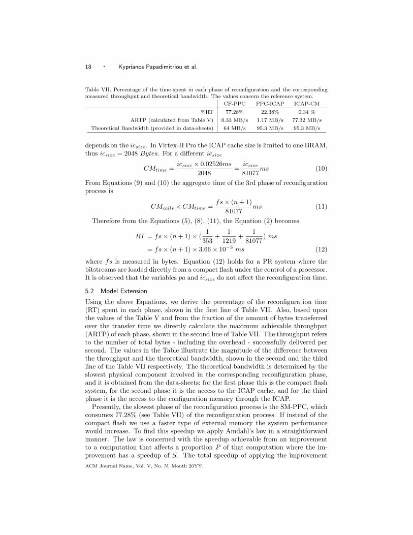
5.2 Model Extension
Using the above Equations, we derive the percentage of the reconfiguration time(RT) spent in each phase, shown in the first line of Table VII. Also, based uponthe values of the Table V and from the fraction of the amount of bytes transferredover the transfer time we directly calculate the maximum achievable throughput(ARTP) of each phase, shown in the second line of Table VII. The throughput refersto the number of total bytes - including the overhead - successfully delivered persecond. The values in the Table illustrate the magnitude of the difference betweenthe throughput and the theoretical bandwidth, shown in the second and the thirdline of the Table VII respectively. The theoretical bandwidth is determined by theslowest physical component involved in the corresponding reconfiguration phase,and it is obtained from the data-sheets; for the first phase this is the compact flashsystem, for the second phase it is the access to the ICAP cache, and for the thirdphase it is the access to the configuration memory through the ICAP.Presently, the slowest phase of the reconfiguration process is the SM-PPC, which
consumes 77.28% (see Table VII) of the reconfiguration process. If instead of thecompact flash we use a faster type of external memory the system performancewould increase. To find this speedup we apply Amdahl’s law in a straightforwardmanner. The law is concerned with the speedup achievable from an improvementto a computation that affects a proportion P of that computation where the im-provement has a speedup of S. The total speedup of applying the improvement
ACM Journal Name, Vol. V, No. N, Month 20YY.
Performance of Partial Reconfiguration in FPGA Systems: A Survey and a Cost Model · 19
is
Speeduptotal =TimeoldTimenew
=1
(1− P ) + PS
(13)
We adjust the problem to our case which is concerned with the reconfigurationspeedup achievable from an improvement to the reconfiguration time that affects aproportion P (which corresponds to the SM-PPC phase) of that reconfiguration timewhere the improvement has a speedup of SSM−PPC , which results in
RTCF
RTSM=
1
(1− P ) + PSSM−PPC
⇔ RTSM = (1− P +P
SSM−PPC)×RTCF (14)
where RTCF and RTSM are the reconfiguration times for the reference systemwith the compact flash and the optimized system with the faster external storagerespectively. For P = 77.28% and by using the Equation (12) to calculate theRTCF , the Equation (14) becomes
RTSM = fs× (n+ 1)× (0.83 +2.83
SSM−PPC)× 10−3 ms (15)
Equation (15) determines the performance margins when the improvement is ap-plied on the first phase of the reconfiguration process. It is more generic thanEquation (12) in that it calculates the reconfiguration time not only for compactflash but for other storage means such as a DDR SDRAM or a ZBT SRAM. If anidentical compact flash to the one of our reference setup is used to load directly thebitstream, the speedup factor would be SSM−PPC = 1. In case a different storageis used, a proportional analysis regarding the performance gained over the compactflash is needed, in order to quantify the SSM−PPC . This analysis along with theusage and effectiveness of the formula is described in Section 6.Equation (15) can be used to calculate the reconfiguration throughput of useful
frames, i.e. without the pad frame. The bitstream size that corresponds to theuseful configuration is BS = fs× n. Thus
useful ARTPSM =BS
RTSM=
n
n+ 1× 10⁶
0.83 + 2.83SSM−PPC
Bytes/s (16)
For the compact flash where SSM−PPC = 1, Equation (16) becomes
useful ARTPCF =n
n+ 1× 0.26 MBytes/s (17)
Similarly, we can compute the reconfiguration throughput of each phase from thecorresponding aggregate reconfiguration time provided in Equations (5),(8) and(11).
5.3 Discussion
Table VII shows clearly that for each phase the throughput vs. the theoreticalbandwidth is degraded considerably. This is due to the distinct components in-volved in the reconfiguration process. For example, in the PPC-ICAP phase, theway the PPC sends the configuration data to the ICAP cache has a negative impacton the reconfiguration time. The processor transfers the data from the PPC local
ACM Journal Name, Vol. V, No. N, Month 20YY.
20 · Kyprianos Papadimitriou et al.
memory to the ICAP cache in a word-by-word fashion, which is iterated until theICAP cache is filled up. We found that to transfer one word 633 PPC cycles arerequired when the PPC runs at 300 MHz, which translates to 2.11 µs. We foundthis time to be fairly constant. The reason this large amount of cycles is needed isthat the transfer from the PPC local memory to the ICAP is bus-based plus thefunction calls residing in the processor local memory are dictated by an ApplicationProgram Interface (API). Moreover the buses operate at 1/3 of the PPC frequency,i.e. 100 MHz, which accounts for the large number of clock cycles in the processor.Also, we measured the time spent for the processor call in the ICAP-CM phase. Forour case where the ICAP cache was 2048 Bytes, 7541 cycles of the PPC running at300 MHz were needed, which translates to 25.26 µs (see Table VI). We repeatedthis measurement and we found it to be constant as well. The above delays addup to the total reconfiguration overhead every time a processor function is called,as the reconfiguration process is not pipelined, but it is controlled with sequentialfunctions. Moreover, the throughput is bounded by the slowest CF-PPC phase,during which several components shown in Figure 3 interact, such as the compactflash, the external System ACE controller, the OPB sysace module, the PPC mem-ory and its memory controller, the bus bridge, and the library maintained in thePPC memory to supervise the transfers.It is obtained from Equation (15) that the parameters pa and icsize are irrelevant.
In particular, the user needs to be aware only of the frame size, fs, and the numberof frames, n, to calculate the expected reconfiguration time. The former is availablein the data-sheets. The quantity fs× (n+ 1) can be replaced with the number ofreconfiguration bytes, rb, of the partial bitstream
where the partial bitstream size is extracted after running the place & route tool,or can be estimated from the synthesis results by using the percentage of occupiedarea and the size of configuration memory of the corresponding FPGA. Finally, theSSM−PPC factor is calculated with a proportional analysis described in the nextSection.
6. VERIFICATION AND USAGE
First we verify the cost model on the base compact flash system, and then we useit to investigate the performance of systems where the bitstreams are loaded froma DDR memory.
6.1 Verification
We used a platform for cryptography applications that we developed on a Virtex-IIPro FPGA with the Xilinx PR design flow. Two cryptography modules, the Ad-vanced Encryption Standard (AES) and the Device Encryption Standard (DES/3DES),are switched on-the-fly without disturbing the remaining logic. The setup is thesame with the one presented in Figure 3 except that the PPC operates at 100 MHzinstead of 300 MHz. The PPC is the reconfiguration controller and the bitstreamsare loaded directly from the compact flash. Table VIII has the details for the twodesigns as well as for the blanking bitstream which is used for power-saving whennone of the cryptography modules is needed. The first two columns show the type
ACM Journal Name, Vol. V, No. N, Month 20YY.
Performance of Partial Reconfiguration in FPGA Systems: A Survey and a Cost Model · 21
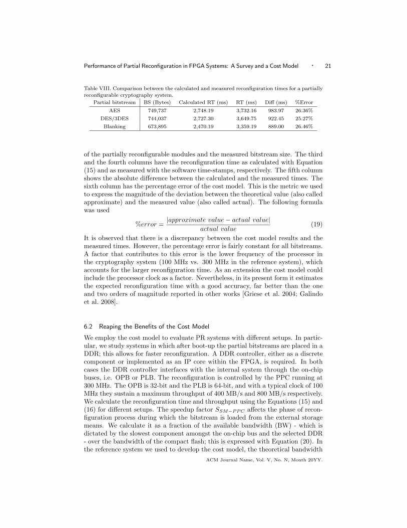
Table VIII. Comparison between the calculated and measured reconfiguration times for a partiallyreconfigurable cryptography system.
of the partially reconfigurable modules and the measured bitstream size. The thirdand the fourth columns have the reconfiguration time as calculated with Equation(15) and as measured with the software time-stamps, respectively. The fifth columnshows the absolute difference between the calculated and the measured times. Thesixth column has the percentage error of the cost model. This is the metric we usedto express the magnitude of the deviation between the theoretical value (also calledapproximate) and the measured value (also called actual). The following formulawas used
%error =|approximate value− actual value|
actual value(19)
It is observed that there is a discrepancy between the cost model results and themeasured times. However, the percentage error is fairly constant for all bitstreams.A factor that contributes to this error is the lower frequency of the processor inthe cryptography system (100 MHz vs. 300 MHz in the reference system), whichaccounts for the larger reconfiguration time. As an extension the cost model couldinclude the processor clock as a factor. Nevertheless, in its present form it estimatesthe expected reconfiguration time with a good accuracy, far better than the oneand two orders of magnitude reported in other works [Griese et al. 2004; Galindoet al. 2008].
6.2 Reaping the Benefits of the Cost Model
We employ the cost model to evaluate PR systems with different setups. In partic-ular, we study systems in which after boot-up the partial bitstreams are placed in aDDR; this allows for faster reconfiguration. A DDR controller, either as a discretecomponent or implemented as an IP core within the FPGA, is required. In bothcases the DDR controller interfaces with the internal system through the on-chipbuses, i.e. OPB or PLB. The reconfiguration is controlled by the PPC running at300 MHz. The OPB is 32-bit and the PLB is 64-bit, and with a typical clock of 100MHz they sustain a maximum throughput of 400 MB/s and 800 MB/s respectively.We calculate the reconfiguration time and throughput using the Equations (15) and(16) for different setups. The speedup factor SSM−PPC affects the phase of recon-figuration process during which the bitstream is loaded from the external storagemeans. We calculate it as a fraction of the available bandwidth (BW) - which isdictated by the slowest component amongst the on-chip bus and the selected DDR- over the bandwidth of the compact flash; this is expressed with Equation (20). Inthe reference system we used to develop the cost model, the theoretical bandwidth
ACM Journal Name, Vol. V, No. N, Month 20YY.
22 · Kyprianos Papadimitriou et al.
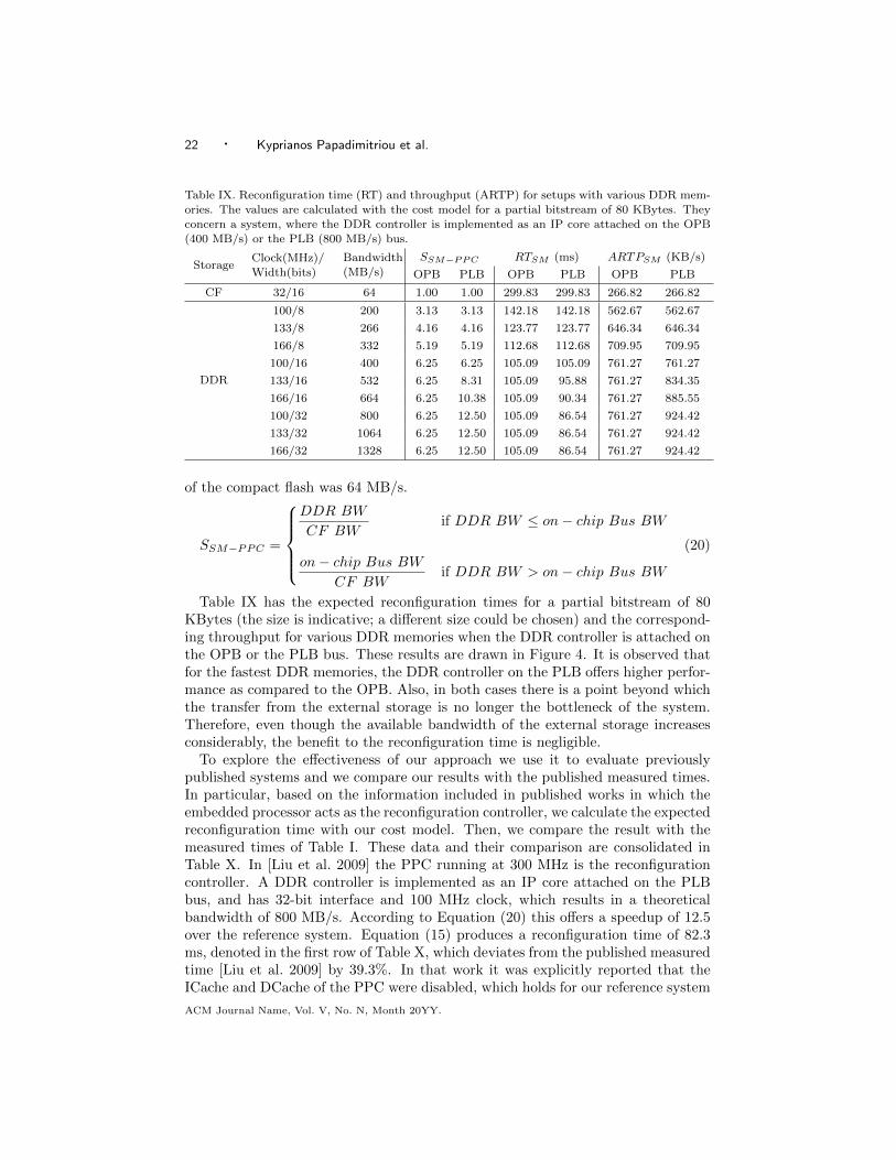
Table IX. Reconfiguration time (RT) and throughput (ARTP) for setups with various DDR mem-ories. The values are calculated with the cost model for a partial bitstream of 80 KBytes. Theyconcern a system, where the DDR controller is implemented as an IP core attached on the OPB(400 MB/s) or the PLB (800 MB/s) bus.
StorageClock(MHz)/Width(bits)
Bandwidth(MB/s)
SSM−PPC RTSM (ms) ARTPSM (KB/s)
OPB PLB OPB PLB OPB PLB
CF 32/16 64 1.00 1.00 299.83 299.83 266.82 266.82
DDR
100/8 200 3.13 3.13 142.18 142.18 562.67 562.67
133/8 266 4.16 4.16 123.77 123.77 646.34 646.34
166/8 332 5.19 5.19 112.68 112.68 709.95 709.95
100/16 400 6.25 6.25 105.09 105.09 761.27 761.27
133/16 532 6.25 8.31 105.09 95.88 761.27 834.35
166/16 664 6.25 10.38 105.09 90.34 761.27 885.55
100/32 800 6.25 12.50 105.09 86.54 761.27 924.42
133/32 1064 6.25 12.50 105.09 86.54 761.27 924.42
166/32 1328 6.25 12.50 105.09 86.54 761.27 924.42
of the compact flash was 64 MB/s.
SSM−PPC =
DDR BW
CF BWif DDR BW ≤ on− chip Bus BW
on− chip Bus BW
CF BWif DDR BW > on− chip Bus BW
(20)
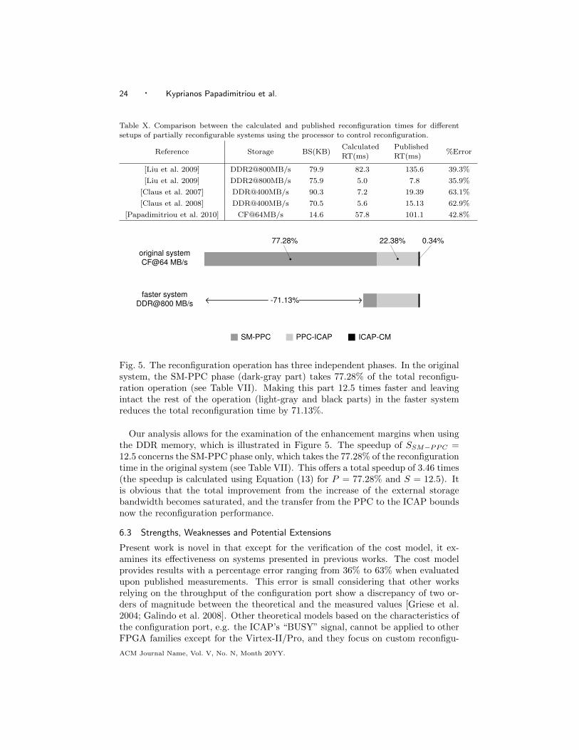
Table IX has the expected reconfiguration times for a partial bitstream of 80KBytes (the size is indicative; a different size could be chosen) and the correspond-ing throughput for various DDR memories when the DDR controller is attached onthe OPB or the PLB bus. These results are drawn in Figure 4. It is observed thatfor the fastest DDR memories, the DDR controller on the PLB offers higher perfor-mance as compared to the OPB. Also, in both cases there is a point beyond whichthe transfer from the external storage is no longer the bottleneck of the system.Therefore, even though the available bandwidth of the external storage increasesconsiderably, the benefit to the reconfiguration time is negligible.To explore the effectiveness of our approach we use it to evaluate previously
published systems and we compare our results with the published measured times.In particular, based on the information included in published works in which theembedded processor acts as the reconfiguration controller, we calculate the expectedreconfiguration time with our cost model. Then, we compare the result with themeasured times of Table I. These data and their comparison are consolidated inTable X. In [Liu et al. 2009] the PPC running at 300 MHz is the reconfigurationcontroller. A DDR controller is implemented as an IP core attached on the PLBbus, and has 32-bit interface and 100 MHz clock, which results in a theoreticalbandwidth of 800 MB/s. According to Equation (20) this offers a speedup of 12.5over the reference system. Equation (15) produces a reconfiguration time of 82.3ms, denoted in the first row of Table X, which deviates from the published measuredtime [Liu et al. 2009] by 39.3%. In that work it was explicitly reported that theICache and DCache of the PPC were disabled, which holds for our reference system
ACM Journal Name, Vol. V, No. N, Month 20YY.
Performance of Partial Reconfiguration in FPGA Systems: A Survey and a Cost Model · 23
0
10
20
30
40
50
60
70
80
90
100
110
120
130
140
150
0 200 400 600 800 1000 1200 1400
External Storage Bandwidth (MB/s)
Re
co
nfig
ura
tio
n T
ime
(m
s)
OPB DDR Cntlr PLB DDR Cntlr
0
100
200
300
400
500
600
700
800
900
1000
0 200 400 600 800 1000 1200 1400
External Storage Bandwidth (MB/s)
Re
co
nfig
ura
tio
n T
hro
ug
hp
ut (K
B/s
)
OPB DDR Cntlr PLB DDR Cntlr
Fig. 4. Reconfiguration time for a partial bitstream of 80 KBytes and the corre-sponding throughput for different DDR memory bandwidths. The data are takenfrom Table IX.
too. In the second system of Table X, the ICache and DCache of the processor wereenabled. According to [Liu et al. 2009] the activation of the processor caches offersan overall enhancement of 16.6 times in the reconfiguration time. Using the costmodel and by dividing the result with 16.6 we obtained the time reported in thesecond row of the Table, equal to 5 ms, which deviates from the published measuredtime by 35.9%. In the same way we extracted the values for all systems of Table X.
ACM Journal Name, Vol. V, No. N, Month 20YY.
24 · Kyprianos Papadimitriou et al.
Table X. Comparison between the calculated and published reconfiguration times for differentsetups of partially reconfigurable systems using the processor to control reconfiguration.
Reference Storage BS(KB)CalculatedRT(ms)
PublishedRT(ms)
%Error
[Liu et al. 2009] DDR2@800MB/s 79.9 82.3 135.6 39.3%
[Liu et al. 2009] DDR2@800MB/s 75.9 5.0 7.8 35.9%
[Claus et al. 2007] DDR@400MB/s 90.3 7.2 19.39 63.1%
[Claus et al. 2008] DDR@400MB/s 70.5 5.6 15.13 62.9%
[Papadimitriou et al. 2010] CF@64MB/s 14.6 57.8 101.1 42.8%
original system
CF@64 MB/s
faster system
DDR@800 MB/s
77.28%
-71.13%
22.38% 0.34%
SM-PPC PPC-ICAP ICAP-CM
Fig. 5. The reconfiguration operation has three independent phases. In the originalsystem, the SM-PPC phase (dark-gray part) takes 77.28% of the total reconfigu-ration operation (see Table VII). Making this part 12.5 times faster and leavingintact the rest of the operation (light-gray and black parts) in the faster systemreduces the total reconfiguration time by 71.13%.
Our analysis allows for the examination of the enhancement margins when usingthe DDR memory, which is illustrated in Figure 5. The speedup of SSM−PPC =12.5 concerns the SM-PPC phase only, which takes the 77.28% of the reconfigurationtime in the original system (see Table VII). This offers a total speedup of 3.46 times(the speedup is calculated using Equation (13) for P = 77.28% and S = 12.5). Itis obvious that the total improvement from the increase of the external storagebandwidth becomes saturated, and the transfer from the PPC to the ICAP boundsnow the reconfiguration performance.
6.3 Strengths, Weaknesses and Potential Extensions
Present work is novel in that except for the verification of the cost model, it ex-amines its effectiveness on systems presented in previous works. The cost modelprovides results with a percentage error ranging from 36% to 63% when evaluatedupon published measurements. This error is small considering that other worksrelying on the throughput of the configuration port show a discrepancy of two or-ders of magnitude between the theoretical and the measured values [Griese et al.2004; Galindo et al. 2008]. Other theoretical models based on the characteristics ofthe configuration port, e.g. the ICAP’s “BUSY” signal, cannot be applied to otherFPGA families except for the Virtex-II/Pro, and they focus on custom reconfigu-
ACM Journal Name, Vol. V, No. N, Month 20YY.
Performance of Partial Reconfiguration in FPGA Systems: A Survey and a Cost Model · 25
ration controllers targeting ICAP full utilization [Claus et al. 2008]. Our approachdoes not rely on the throughput of the configuration port, nor on characteristicsthat vary with the FPGA technology, e.g. behavior of “BUSY” signal differs inVirtex-II, Virtex-4 and Virtex-5 FPGAs.The proposed cost model can be augmented with more factors in the same way
the simple model for the compact flash on the reference system was extended tosupport other types of external memories. Specifically, the second part of Section 5was devoted to extend the model with the optimization factor SSM−PPC . Followingthe same concept, Equation (15) can be enriched with optimization factors forthe PPC-ICAP and the ICAP-CM phases (namely SPPC−ICAP and SICAP−CM
respectively). To do this further experimentation with a different setup is needed.In particular, Figure 4 shows that after a specific point the larger bandwidth ofthe external memory does not necessarily result in a higher throughput. Instead,the PPC-ICAP phase becomes the bottleneck as illustrated in Figure 5. Therefore,other alternatives can be explored such as the usage of the On Chip Memory (OCM)instead of the PLB memory, which is likely to provide lower latency communication.Furthermore, the cost model can be extended with a factor that relates to theimpact of changing the processor clock. Experimentation will quantify this as wellto reduce even more the uncertainty for the expected reconfiguration time.The presented approach considers systems in which the reconfiguration is con-
trolled by the processor. Therefore, it serves users who desire to pre-evaluate theirsystem without putting the effort to implement a custom reconfiguration controller.The values we used to develop the cost model were obtained with real measurementsprevious published in [Papadimitriou et al. 2007; 2010]. Even though they are ofsmall scale they were proven adequate to foresee well the reconfiguration perfor-mance. After we gained insights from the reference system, we developed the modelwithout delving into details such as the latency of the distinct components involvedin the reconfiguration process. The only factors that someone should consider of iswhether the processor is the reconfiguration controller and its caches are enabled,and the type of external storage the bitstreams are loaded from. In particular, fora given system setup, simple characteristics gathered from data-sheets such as theavailable bandwidth, the frame size, and the bitstream size are enough to predictthe reconfiguration time.
7. DISCUSSION SUMMARY
This paper delivers an up-to-date survey and an exploration of the parametersaffecting the reconfiguration performance. A real system is analyzed to identifythe features that increase reconfiguration speed. Using this system as referencea simple cost model for the early prediction of reconfiguration time is developed.The model is verified, then used to evaluate several “real-world” systems, and theresults are compared with published measurements. Also, the study quantifies theimprovement of reconfiguration performance given the speedup of data transferoffered by the DDR memory over the compact flash. Finally, the strengths andweaknesses of our approach are discussed.We conclude that experimental evaluation is necessary for revealing the details of
system-level operation. With data gathered from experiments we devised a method
ACM Journal Name, Vol. V, No. N, Month 20YY.
26 · Kyprianos Papadimitriou et al.
and a cost model currently applied in a category of real PR systems, which can beenhanced with more parameters to broaden its range of applicability.Nowadays FPGA platforms are delivered as end-products and the benefits of
partial reconfiguration technology are still being explored in numerous applicationdomains. With the proposed model an opportunity arises for people not involvedwith partial reconfiguration yet but are interested to study whether their applica-tions can benefit from this technology. We aim to assist researchers from differentdomains such as telecommunications, cryptography and networking to estimate thereconfiguration overhead without entering the complex and rigid PR design flow,and also to make effective choices of the system setup. Hence, based on specificconstraints they can decide if it is worthwhile to proceed in designing an applicationwith PR technology by either assigning this task to experts having the know-howof PR design flow, or putting this effort on their own.
ACKNOWLEDGMENT
The authors wish to thank Dr. Christoforos Kachris for his valuable feedback thathelped improving the initial manuscript. This work was partly funded by Secure,Mobile visual sensor networks ArchiTecture research project (SMART, project num-ber: 100032), funded within the ARTEMIS Joint Technology Initiative as a JointUndertaking project between the European Commission, the Member States andthe ARTEMIS Industrial Association (ARTEMISIA).
REFERENCES
Claus, C., Muller, F. H., Zeppenfeld, J., and Stechele, W. 2007. A New Framework toAccelerate Virtex-II Pro Dynamic Partial Self-Reconfiguration. In Proceedings of the IEEEInternational Parallel and Distributed Processing Symposium (IPDPS). 1–7.
Claus, C., Zhang, B., Stechele, W., Braun, L., Hubner, M., and Becker, J. 2008. A Multi-Platform Controller Allowing for Maximum Dynamic Partial Reconfiguration Throughput. InProceedings of the IEEE International Conference on Field Programmable Logic and Applica-tions (FPL). 535–538.
Delahaye, J.-P., Palicot, J., Moy, C., and Leray, P. 2007. Partial Reconfiguration of FP-GAs for Dynamical Reconfiguration of a Software Radio Platform. In Mobile and WirelessCommunications Summit, 2007. 16th IST. 1–5.
Fong, R. J., Harper, S. J., and Athanas, P. M. 2003. A Versatile Framework for FPGAField Updates: An Application of Partial Self-Reconfiguation. In Proceedings of the IEEEInternational Workshop on Rapid System Prototyping (RSP). 117–123.
French, M., Anderson, E., and Kang, D.-I. 2008. Autonomous System on a Chip Adaptationthrough Partial Runtime Reconfiguration. In Proceedings of the IEEE International Symposiumon Field-Programmable Custom Computing Machines (FCCM). 77–86.
Galindo, J., Peskin, E., Larson, B., and Roylance, G. 2008. Leveraging Firmware in Mul-tichip Systems to Maximize FPGA Resources: An Application of Self-Partial Reconfiguration.In Proceedings of the International Conference on Reconfigurable Computing and FPGAs (Re-ConFig). 139–144.
Gelado, I., Morancho, E., and Navarro, N. 2006. Experimental Support for ReconfigurableApplication-Specific Accelerators. In Proceedings of the Workshop on the Interaction betweenOperating Systems and Computer Architecture (WIOSCA), in conjuction with the Interna-tional Symposium on Computer Architecture (ISCA). 50–57.
Gholamipour, A. H., Eslami, H., Eltawil, A., and Kurdahi, F. 2009. Size-Reconfiguration De-lay Tradeoffs for a Class of DSP Block in Multi-mode Communication Systems. In Proceedings
ACM Journal Name, Vol. V, No. N, Month 20YY.
Performance of Partial Reconfiguration in FPGA Systems: A Survey and a Cost Model · 27
of the IEEE International Symposium on Field-Programmable Custom Computing Machines(FCCM). 71–78.
Griese, B., Vonnahme, E., Porrmann, M., and Ruckert, U. 2004. Hardware Support for Dy-namic Reconfiguration in Reconfigurable SoC Architectures. In Proceedings of the InternationalWorkshop on Field Programmable Logic and Applications (FPL). 842–846.
Hauck, S. 1998. Configuration Prefetch for Single Context Reconfigurable Coprocessors. In Pro-ceedings of the IEEE International Symposium on Field Programmable Gate Arrays (FPGA).65–74.
Hsiung, P.-A., Lin, C.-S., and Liao, C.-F. 2008. Perfecto: A Systemc-based Design-space Ex-ploration Framework for Dynamically Reconfigurable Architectures. ACM Transactions onReconfigurable Technology and Systems 1, 3, 1–30.
IBM Inc. 2000. 128-bit Processor Local Bus. Architecture Specifications Version 4.6.
IBM Inc. 2001. On-Chip Peripheral Bus. Architecture Specifications Version 2.1.
IBM Inc. 2006. Device Control Register Bus 3.5. Architecture Specifications.
Kachris, C. and Vassiliadis, S. 2006. Performance Evaluation of an Adaptive FPGA for NetworkApplications. In Proceedings of the IEEE International Workshop on Rapid System Prototyping(RSP). 54–62.
Liu, M., Kuehn, W., Lu, Z., and Jantsch, A. 2009. Run-Time Partial Reconfiguration SpeedInvestigation and Architectural Design Space Exploration. In Proceedings of the IEEE Inter-national Workshop on Field Programmable Logic and Applications (FPL). 498–502.
Lund, K. 2004. PLB vs. OCM Comparison Using the Packet Processor Software. ApplicationNote: Virtex-II Pro Family XAPP644 (v1.1), Xilinx.
Lysaght, P., Blodget, B., Mason, J., Young, J., and Bridgeford, B. 2006. Enhanced Archi-tectures, Design Methodologies and CAD Tools for Dynamic Reconfiguration on Xilinx FPGAs.In Proceedings of the IEEE International Conference on Field Programmable Logic and Appli-cations (FPL). 1–6.
Manet, P., Maufroid, D., Tosi, L., Gailliard, G., Mulertt, O., Ciano, M. D., Legat, J.-D., Aulagnier, D., Gamrat, C., Liberati, R., Barba, V. L., Cuvelier, P., Rousseau, B.,and Gelineau, P. 2008. An Evaluation of Dynamic Partial Reconfiguration for Signal andImage Processing in Professional Electronics Applications. EURASIP Journal on EmbeddedSystems 2008, 11 pages.
McKay, N., Melham, T., and Susanto, K. 1998. Dynamic specialisation of XC6200 FP-GAs by partial evaluation. In Proceedings of the IEEE International Symposium on Field-Programmable Custom Computing Machines (FCCM). 308–309.
Moller, L., Soares, R., Carvalho, E., Grehs, I., Calazans, N., and Moraes, F. 2006. In-frastructure for Dynamic Reconfigurable Systems: Choices and Trade-offs. In Proceedings ofthe International Symposium on Integrated Circuits and Systems Design, SBCCI. 44–49.
Noguera, J. and Kennedy, I. O. 2007. Power Reduction in Network Equipment through Adap-tive Partial Reconfiguration. In Proceedings of the IEEE International Workshop on FieldProgrammable Logic and Applications (FPL). 240–245.
Papadimitriou, K., Anyfantis, A., and Dollas, A. 2007. Methodology and Experimental Setupfor the Determination of System-level Dynamic Reconfiguration Overhead. In Proceedingsof the IEEE International Symposium on Field-Programmable Custom Computing Machines(FCCM). 335–336.
Papadimitriou, K., Anyfantis, A., and Dollas, A. 2010. An Effective Framework to EvaluateDynamic Partial Reconfiguration in FPGA Systems. IEEE Transactions on Instrumentationand Measurement 59, 6, 1642–1651.
Papadimitriou, K. and Dollas, A. 2006. Performance Evaluation of a Preloading Model inDynamically Reconfigurable Processors. In Proceedings of the IEEE International Conferenceon Field Programmable Logic and Applications (FPL). 901–904.
Paulsson, K., Hubner, M., and Becker, J. 2008. Cost-and Power Optimized FPGA based Sys-tem Integration: Methodologies and Integration of a Low-Power Capacity-based MeasurementApplication on Xilinx FPGAs. In Proceedings of the Design, Automation and Test in Europe(DATE). 50–55.
Santambrogio, M. D., Rana, V., and Sciuto, D. 2008. Operating System Support for On-line Partial Dynamic Reconfiguration Management. In Proceedings of the IEEE InternationalWorkshop on Field Programmable Logic and Applications (FPL). 455–458.
Xilinx Inc. 2006. OPB HWICAP (v1.00.b) Product Specification DS280 July 26, 2006.
Xilinx Inc. 2007a. Virtex-II Pro and Virtex-II Pro X FPGA User Guide. Datasheet. UG012(v4.2) November 5, 2007.
Xilinx Inc. 2007b. XPS HWICAP (v1.00.a) Product Specification DS586 November 05, 2007.