PERFORMANCE OF SILICONE RUBBER MATERIALS UNDER HIGH VOLTAGE DIRECT CURRENT USING THE INCLINED PLANE TEST Nishal Mahatho A research report submitted to the faculty of Engineering and the Built Environment, University of the Witwatersrand, in fulfilment of the requirements for the degree of Master of Science of Engineering Johannesburg, August, 2014
Transcript
PERFORMANCE OF SILICONE RUBBER
MATERIALS UNDER HIGH VOLTAGE DIRECT
CURRENT USING THE INCLINED PLANE TEST
Nishal Mahatho
A research report submitted to the faculty of Engineering and the Built Environment, University of the Witwatersrand, in fulfilment
of the requirements for the degree of Master of Science of Engineering
Johannesburg, August, 2014
Page | ii
Abstract
There are many HVDC schemes around the world operating at various voltage levels ranging
from ±200kV to ±800kV dc. The choice of insulator types and level of insulation varies with
voltage levels and environmental conditions through which the substations and transmission
lines traverse.
As in the case for ac lines, polymeric insulators were introduced on dc lines with a view to
improved pollution performance and reduction of damage from vandalism. Another possible
reason is that, generally, the price for a full dc glass string is higher than that of a similar
voltage polymeric insulator unit.
Polymeric insulators, comprising of silicone rubber (SiR) material filled with alumina
trihydrate (ATH), have the ability of maintaining and transferring their hydrophobic property
to the pollution layer that may collect on the surface, which gives them their superior
pollution performance. A concern regarding the use of polymeric insulators is the ageing of
the SiR material, which when stressed under certain ambient conditions may temporarily lose
its hydrophobic property. During this period local discharge activity (corona discharges or
surface leakage current flow) may lead to tracking on the surface and even erosion of the
material. With sustained activity this may eventually lead to permanent degradation of the
material and allow moisture ingress to the fiber glass core of the insulator. The combination
of moisture ingress and the high electric fields may ultimately lead to failure of the insulator
by mechanisms such as brittle fracture, flash-under, etc. as seen in various cases reported on
ac lines.
The performance, and in particular the ageing of polymeric insulators under HVDC stress, is
an area that has not been researched as extensively as for HVAC stress. Factors such as
pollution catch and accumulation, material composition, space charge effects and line
polarity have yet to be explicitly evaluated. This research focuses on the accelerated ageing
of silicon rubber when subjected to dc stress, taking polarity into account. The results of
inclined plane tests, as per IEC60587:2007, and the materials analyses on the silicone rubber
are presented. The tests indicate that by using the standard ac guidelines, samples subjected to
equivalent dc stress fail quicker than ac samples. This dissertation presents the results of
electrical testing, and analyses of the materials after degradation using known chemical
analysis techniques.
Page | iii
Declaration
I declare that this dissertation is my own, unaided work. It is being submitted for the Degree of Master of Science in the University of the Witwatersrand, Johannesburg. It has not been submitted before for any degree or examination in any other University.
Signed on August 25, 2014
_______________________ Nishal Mahatho
Page | iv
Acknowledgements I dedicate this dissertation to my wife, Prabashnie, and my sons, Rushil and Sudhay, for their unwavering support and understanding. My sincere gratitude to:
God, for the opportunity and grace to complete this work
My parents for their constant support
My supervisor, Professor Ian Jandrell, for his wisdom, support and understanding
My colleagues and friends, Nishanth Parus and Thavenesen Govender, for their assistance and guidance
Mr David Muller, Mr Shaun Aitken and the staff at Pfisterer, South Africa for the use of their Incline Plane Test facility, and assistance with samples and testing
Dr James-Wesley Smith and Dr Sreejarani Pillai for the assistance and guidance with the material sampling
Mr Jacques Calitz for his assistance with tensile testing
Page | v
Table of Contents 1 Introduction ........................................................................................................................ 2
3 Cross-sectional view of the control sample and the FTIR spectrum 5
4 Discharge activity noted on voltage application 5
5 Track marks on the material surface and Infra-red image of heating
caused by leakage current flow 6
6 Sample 5 after 6 hours of energisation and sample after cleaning 6
7 Cross-sectional view of the ac sample and the comparison in FTIR scan 7
8 Burning on sample 2 at ground electrode and erosion noted on sample 2 7
9 All three samples showing signs of severe erosion 8
10 Formation of the arc root, and the starting of erosion 8
11 Severe erosion on sample 2 after 42 minutes 9
12 Cross-sectional views of +4.5kV dc and -4.5kV dc 9
13 FTIR comparisons between +4.5kV dc (pink) and -4.5kV dc (blue) against
the control (green) 10
14 Arcing and the starting of erosion in sample 2, and small flames
observed after 40 minutes 10
15 Sample 2 burnt all the way through, and all 3 samples after the test. 11
16 Development of arc roots with scintillations across the sample surface 11
17 The samples at the end of the negative 6.3 kV dc test and, sample 3
after cleaning 12
18 Cross-sectional views of +6.3 kV dc and -6.3 kV dc 12
19 FTIR comparisons between +6.3kV dc (orange) and -6.3kV dc (blue)
against the control (green) 13
B.1 Assembly of the electrodes – contaminant flows from top to bottom 24
Page | viii
B.2 Actual incline plane test setup used for this study 24
B.3 Circuit diagram for positive dc setup 25
B.4 Circuit diagram for negative dc setup 25
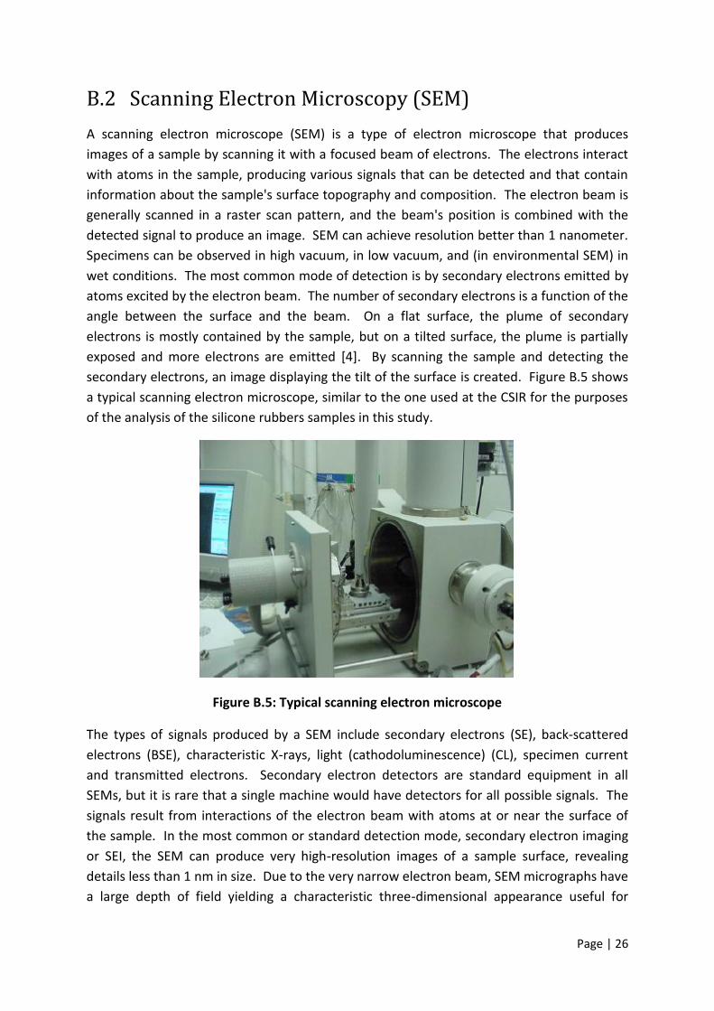
B.5 Typical scanning electron microscope 26
B.6 Schematic diagram of a SEM 28
B.7 SEM images of the silicone rubber control sample 28
B.8 Schematic diagram of a Michelson interferometer, configure for FTIR 30 B.9 FTIR spectrum of the control sample of silicone rubber 30 B.10 EDS scan of the silicone rubber control sample used for the IPT tests 32
C.1 AC test samples prior to energisation 33
C.2 Discharge activity at start 34
C.3 Discharge activity 34
C.4 Visible “track” marks 34
C.5 C.5 34
C.6 C.6 34
C.7 C.7 34
C.8 Greater degree of blackening 35
C.9 Yellow-brown discolouration 35
C.10 C.10 35
C.11 C.11 35
C.12 IR image of leakage current 35
C.13 IR image 35
C.14 Erosion and arc spots at ground end 36
C.15 Sample 5 after energisation 36
C.16 Sample 5 after being cleaned 36
C.17 More vigorous scintillations 37
Page | ix
C.18 Development of arc 37
C.19 Discolouration along length 37
C.20 Burning of sample 2 37
C.21 Erosion at ground electrode 37
C.22 Formation of arc root on sample 3, TP1 38
C.23 Erosion on sample 2 and sample 3 38
C.24 Length of erosion on sample 3 progressed to 60% 39
C.25 Flame observed on sample 2 39
C.26 Samples after testing 39
C.27 Leakage current graph: +4.5 kV dc 40
C.28 Surface scintillations 40
C.29 C.29 40
C.30 Partials arcs observed 41
C.31 Beginning of arc root on sample 2 41
C.32 Arc root on Sample 1 41
C.33 Burning on sample 2 41
C.34 Erosion approx. 50% of gap 41
C.35 Sample 2 after 42 minutes 41
C.36 DC samples showing varying stages of erosion 42
C.37 Leakage current graph: -4.5 kV dc 42
C.38 “Long” scintillations observed 43
C.39 “Long” arcs observed 43
C.40 Brighter arcs 43
C.41 Erosion on sample 2 43
C.42 Arc completely bridging gap 44
C.43 Arc bridging 60% on sample 1 44
Page | x
C.44 Sample 2 burning 44
C.45 Sample 2 after 58 minutes 44
C.46 Leakage current graph: +6.3 kV dc 45
C.47 Scintillations across surface 45
C.48 C.48 45
C.49 Formation of arc roots 46
C.50 C.50 46
C.51 No erosion observed 46
C.52 Blackening on surface 46
C.53 Samples after test 47
C.54 Sample 3 after cleaning 47
C.55 Leakage current graph: -6.3 kV dc 47
D.1 SEM analysis of the control sample 50 D.2 SEM analysis of ac samples 51 D.3 SEM analysis of positive 4.5 kV dc sample 52 D.4 SEM analysis of negative 4.5 kV dc sample 52 D.5 SEM analysis of positive 6.3 kV dc sample 53 D.6 SEM analysis of negative 6.3 kV sample 53 D.7 FTIR spectra of the control sample 54 D.8 FTIR spectrum of AC sample – 1cm away from damage area 55 D.9 FTIR spectrum of AC sample – damage area 55 D.10 FTIR of positive 4.5 kV dc sample – 1 cm away from damage area 56 D.11 FTIR of positive 4.5 kV dc sample – damage area 56 D.12 FTIR of negative 4.5 kV dc sample – 1cm away from damage area 57 D.13 FTIR of negative 4.5 kV dc sample – damage area 57
Page | xi
D.14 FTIR of positive 6.3 kV dc sample – 1 cm away from damage area 58 D.15 FTIR of positive 6.3 kV dc sample – damage area 58 D.16 FTIR of negative 6.3 kV dc sample – 1 cm away from damage area 59 D.17 FTIR of negative 6.3 kV dc sample – damage area 59 D.18 EDS scan of the control sample with two linescans 60 D.19 EDS scan of the ac sample 60 D.20 EDS Scan of positive 4.5 kV dc sample 61 D.21 EDS scan of negative 4.5 kV dc sample 61 D.22 EDS scan of positive 6.3 kV dc sample 62 D.23 EDS Scan of negative 6.3 kV dc sample 62 D.24 XRD result for the control sample 63 D.25 XRD result for the ac sample 63 D.26 XRD result for the positive 4.5 kV dc sample 64 D.27 XRD result for the negative 4.5 kV dc sample 64 D.28 XRD result for the positive 6.3 kV dc sample 65 D.29 XRD result for the negative 6.3 kV dc sample 65 D.30 Tensile test on damaged / aged samples 66
Page | xii
List of Tables 1 Summary of all the IPT tests 14
C.1 Current measurements – positive 4.5 kV dc 40
C.2 Current measurements – negative 4.5 kV dc 42
C.3 Current measurements – positive 6.3 kV dc 45
C.4 Current measurements – negative 6.3 kV dc 47
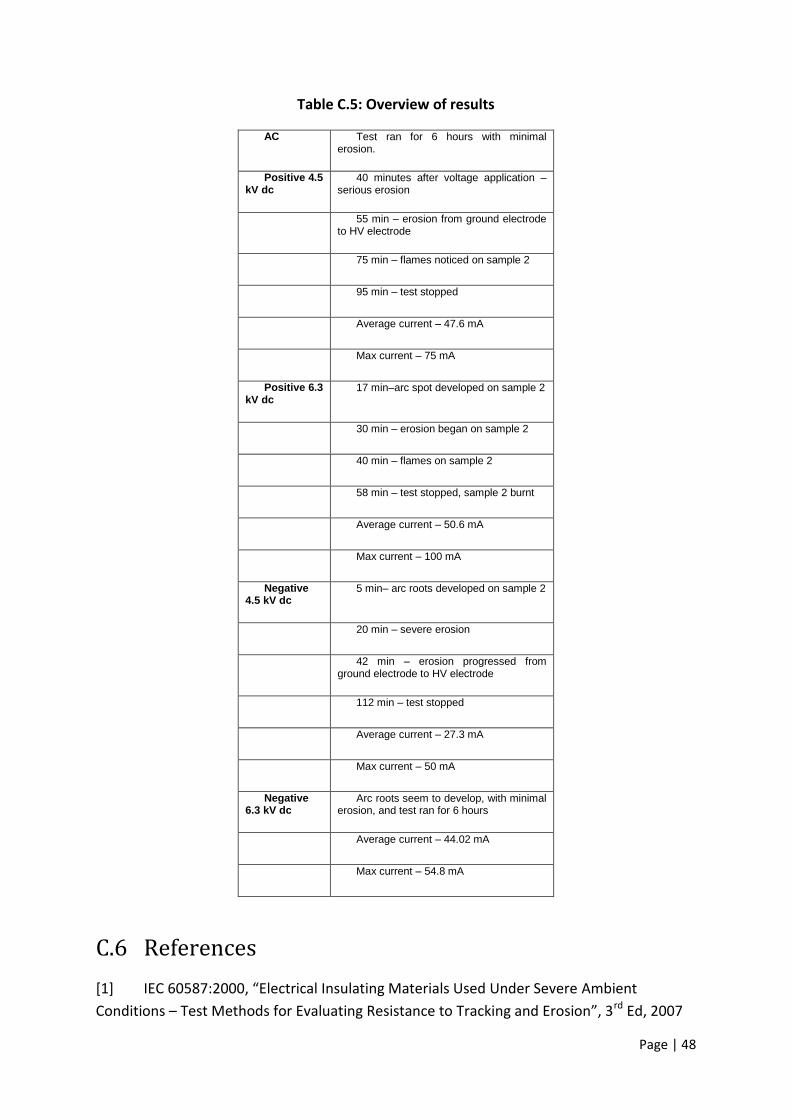
C.5 Overview of results 48
Page | xiii
List of Symbols and Acronyms ac alternating current dc direct current rms root mean square kV kilo-volt CSIR Centre for Scientific and Industrial Research CC1 CoroCam 1 IR Infra-Red UV Ultra Violet mA milli-amperes TP test position % percentage mm millimetres HTV High Temperature Vulcanised RTV Room Temperature Vulcanised SiR Silicone Rubber HV High Voltage mS milli-Siemens FTIR Fourier Transform Infra-Red Spectroscopy EDX Energy Dispersive X-Ray XRD X-Ray Diffraction µ micro LMW Low Molecular Weight
Page | xiv
ATH Alumina Tri-Hydrate ESCA Electron Spectroscopy for Chemical Analysis XPS X-Ray Photoelectron Spectroscopy TGA Thermogravimetric Analysis nm nanometers W watts Hz hertz eV electron volts
Page | xv
Preface This research dissertation presents the work in the form of a short paper, followed by a number of appendices. The paper proposes the hypothesis and presents a discussion on the testing, results obtained and analysis. The appendices provide a more in depth explanation of the work covered, where each appendix is referenced separately. A short description of the appendices follows.
Appendix A – Literature Review Presents the results and summary of the literature reviewed.
Appendix B – Measuring Equipment and Test Methodology This section describes the various methods and techniques used for the testing and analysis of the silicone rubber samples.
Appendix C – Results of Electrical Testing This section provides the results and analysis of the electrical testing using the Incline Plane Test method as defined by IEC 60587. The results for each series of tests are presented and discussed in this section.
Appendix D – Results and Analysis of Materials Testing This section considers the materials analysis of the HTV silicon rubber material used in the inclined plane test under ac and dc voltage application, utilising the various techniques available.
PERFORMANCE OF SILICONE RUBBER MATERIALS UNDER HIGH VOLTAGE
DIRECT CURRENT USING THE INCLINED PLANE TEST
N. Mahatho School of Electrical and Information Engineering, University of the Witwatersrand, Johannesburg,
South Africa
Abstract: There are several High Voltage Direct Current (HVDC) schemes in existence, many of which have been traditionally insulated with glass insulator strings. Due to its hydrophobic nature, the later development of polymeric insulators provided better pollution performance. The performance, and in particular the ageing of polymeric insulators under HVDC stress, is an area that has not been researched as extensively as for HVAC stress. Factors such as pollution catch and accumulation, material composition, space charge effects and line polarity have yet to be explicitly evaluated. This research focuses on the accelerated ageing of silicon rubber when subjected to dc stress, taking polarity into account. The results of inclined plane tests, as per IEC60587:2007, and the materials analyses on the silicone rubber are presented. The tests indicate that by using the standard ac guidelines, samples subjected to equivalent dc stress fail quicker than ac samples. It was observed that the positive dc showed higher levels of current than the negative tests, and the erosion is more severe. The negative dc test at 4.5 kV showed severe erosion similar to the positive dc case, but the negative 6.3 kV dc test ran for the full 6 hours with minimal erosion. The SEM analysis showed marked differences between the damaged/burnt areas of the materials as expected, while the FTIR indicated an attenuation of the peaks in the 3600 to 3300 wave number (in the dc energised samples), when compared to the virgin material. EDS analysis showed a decrease in the silicon and aluminium content in the damaged areas.
Page | 2
1 Introduction
There are many HVDC schemes around the world operating at various voltage levels ranging
from ±200 kV to ±800 kV dc. The choice of insulator types and level of insulation varies with
voltage levels and environmental conditions through which the substations and
transmission lines traverse.
As in the case for ac lines, polymeric insulators were introduced on dc lines with a view to
improved pollution performance and reduction of damage from vandalism. Another
possible reason is that, generally, the price for a full dc glass string is higher than that of a
similar voltage polymeric insulator unit [1].
Polymeric insulators, with silicone rubber (SiR) material, have the ability of maintaining and
transferring their hydrophobic property to the pollution layer that may collect on the
surface, which gives them their superior pollution performance. A concern regarding the
use of polymeric insulators is the ageing of the SiR material, which when stressed under
certain ambient conditions may temporarily lose its hydrophobic property. During this
period local discharge activity (corona discharges or surface leakage current flow) may lead
to tracking on the surface and even erosion of the material. With sustained activity this may
eventually lead to permanent degradation of the material and allow moisture ingress to the
fiber glass core of the insulator. The combination of moisture ingress and the high electric
fields may ultimately lead to failure of the insulator by mechanisms such as brittle fracture,
flash-under, etc. as seen in various cases reported on ac lines.
2 Hypothesis
It is hypothesised that the performance of the polymeric insulator material under dc stress,
from a tracking, erosion and corona activity perspective, will be inferior compared to the
respective ac scenario. This is possibly due to the aggressive nature of the dc stress and the
fact that the dc voltage is non-cyclical in nature.
3 Test Setup and Methodology
In order to conduct the experiment, an inclined plane test (IPT) setup was utilised, shown in Figure 1. The IPT chamber is supplied by a single phase 230 V / 12 kV step-up transformer. This setup was used for the ac tests. For the positive dc tests a Spellman 50 kV dc, 80 mA stand-alone supply was used to charge a smoothing capacitor of 66 µF coupled to the necessary peripheral equipment for protection and switching. For the negative dc tests a half wave rectifier circuit was constructed. This setup used an 80 kV (peak inverse voltage), 500 mA diode arrangement in series with a 100 Ω resistor. This was then used to charge the 66 µF capacitor, and coupled to the necessary peripheral equipment.
The test setup and methodology was as per IEC 60587:2007(E) [2].
Page | 3
The insulator sample is mounted on an insulated stand at an angle of 45° to the horizontal. The high voltage (HV) and ground electrodes are connected to the top and bottom of the sample respectively, as shown in Figure 1.
Figure 1: Inclined plane test setup
The sample surface is continually wetted with a contaminant consisting of 0,1% (by mass) of ammonium chloride and 0,02% (by mass) of a non-ionic wetting agent, isooctylphenoxpolyethoxyethanol [(C14H22O(C2H4O)n); n=9-10], in distilled water [2]. The contaminant runs from the HV electrode to the ground electrode. The required conductivity of the contaminant, according to IEC 60587, should be 2.53 mS/cm. The conductivity of the contaminant used for all the tests was 2.7 mS/cm. Experiments conducted by Seifert et al [3] showed maximum erosion with a contaminant conductivity of 2.5 mS/cm (at 5.5 kV).
When a test voltage is applied to the samples, leakage currents flow through the contaminant on the surface of the samples. This current flow causes a heating effect which then results in the contaminant drying up close to the ground electrode. Dry bands start to develop in this area, which result in arcing and discharges that lead to erosion in the vicinity of the ground electrode [2, 4]. For this work, the constant tracking voltage method of the IEC 60587 standard was used.
4 Test materials and evaluation
4.1 Test Material
All the samples used for the ac and dc tests were manufactured from the same batch of silicone rubber, thus ensuring consistency in the test samples. The samples were manufactured from high temperature vulcanised (HTV) silicone rubber in slabs of approximately 118 x 50 x 6 mm. Figure 2 shows the virgin test samples (ac test samples prior to energisation).
Contaminant
HV Electrode
Ground Electrode
Sample
Page | 4
Figure 2: AC test samples prior to energisation
Prior to testing, each sample was thoroughly cleaned using ethanol, and mounted carefully to prevent contamination.
4.2 Evaluation Methodology
The IEC 60587 standard calls for 5 samples to be used for the testing, however, due to test set limitations 4 samples were energised in the ac test and 3 for each of the dc tests. The test voltage chosen for the ac test was 4.5 kV (rms). For the dc tests it was decided to use the equivalent ac rms voltage (i.e. 4.5 kV) as well as the ac peak voltage (6.3 kV). Thus separate tests were carried out at 4.5 and 6.3 kV positive dc, and 4.5 and 6.3 kV negative dc. For all tests the contaminant was allowed to flow for 10 minutes, to ensure steady flow as per IEC 60587, before the respective voltage was applied. In total 16 samples were tested for the 5 voltage levels investigated.
For the ac and dc tests, visual observations and video recordings were conducted, as well as infra-red (utilising a CSIR Multi Spectral camera) and ultra-violet observations (using a night corona camera- CSIR CCI). In addition, for the dc tests, a multimeter was connected in series with sample 1 (in test position 1 – test positions were numbered from 1-5 from right to left) to measure the leakage current. The current was manually recorded at periodic intervals throughout the tests.
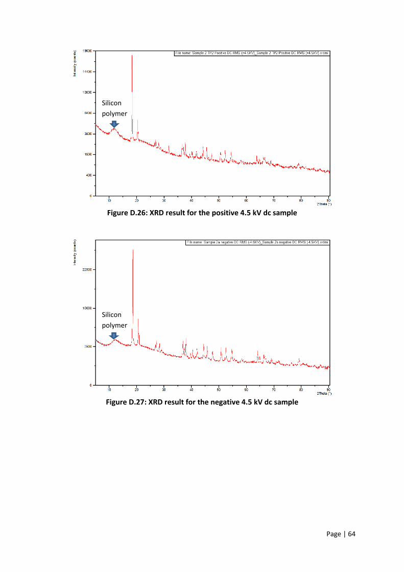
The materials analyses on the samples were conducted utilising equipment from the CSIR, and included Scanning Electron Microscopy (SEM), Energy Dispersive Spectrography (EDS), Fourier Transform Infra-Red (FTIR) and X-Ray Diffraction (XRD). Some of these results are presented and explained in the paper.
5 Results and Discussion
The results for each series of tests are presented and discussed in this section.
5.1 Control and AC Test
The control sample was a virgin sample of silicone rubber material as shown in Figure 2.
Page | 5
(a) (b)
Figure 3: (a) Cross-sectional view of the control sample and (b) the FTIR spectrum
Cross sections of control samples show a relatively uniform surface texture with occasional large inclusions, shown in Figure 3a. FTIR spectra in Figure 3b showed characteristic N-H stretching peaks between 3200 and 3500 wave numbers (w/n), C-H stretching below 3000 and C-O / C-H stretching between 1500 and 1000 w/n
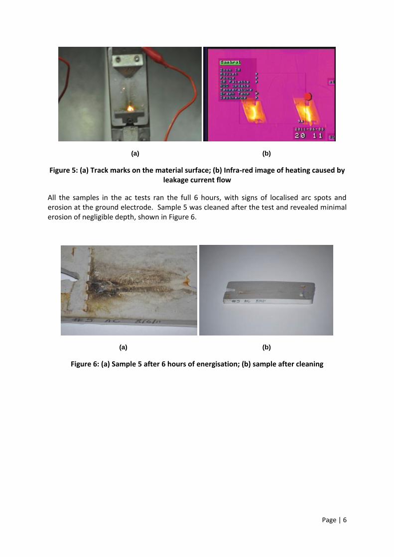
In the ac test 4.5 kV rms was applied to the samples, and 4 samples were energised (test positions 1, 2, 4 & 5). Scintillations and discharge activity was noted on voltage application, shown in Figure 4. After approximately 45 minutes of energisation it was observed that ‘track’ marks were clearly visible on the samples (along the contamination path). Figure 5a shows the ‘track’ marks and the beginning of the local arc spots and erosion. Figure 5b shows the heating caused by the leakage current activity.
Figure 4: Discharge activity noted on voltage application
TP1 TP2 TP3 TP4
TP5
Page | 6
(a) (b)
Figure 5: (a) Track marks on the material surface; (b) Infra-red image of heating caused by leakage current flow
All the samples in the ac tests ran the full 6 hours, with signs of localised arc spots and erosion at the ground electrode. Sample 5 was cleaned after the test and revealed minimal erosion of negligible depth, shown in Figure 6.
(a) (b)
Figure 6: (a) Sample 5 after 6 hours of energisation; (b) sample after cleaning
Page | 7
Materials Analysis
(a) (b)
Figure 7: (a) Cross-sectional view of the ac sample and (b) the comparison in FTIR scan
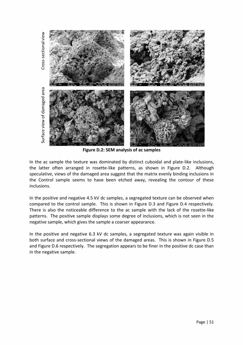
The ac sample had a surface texture that was characterised by distinct cuboidal and plate-like inclusions (Figure 7a). Figure 7b shows the spectrum from the damaged spot (purple spectrum) resembling that of the control (green spectrum) except for the appearance of peaks above 1500 w/n. There are also peaks between 3300 and 3000 that are not seen in the control sample.
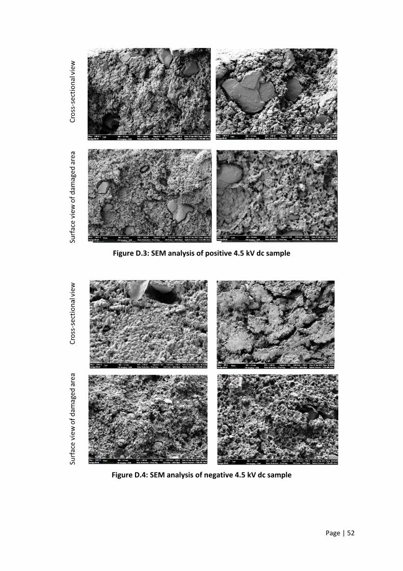
5.2 Positive and negative dc test: 4.5 kV
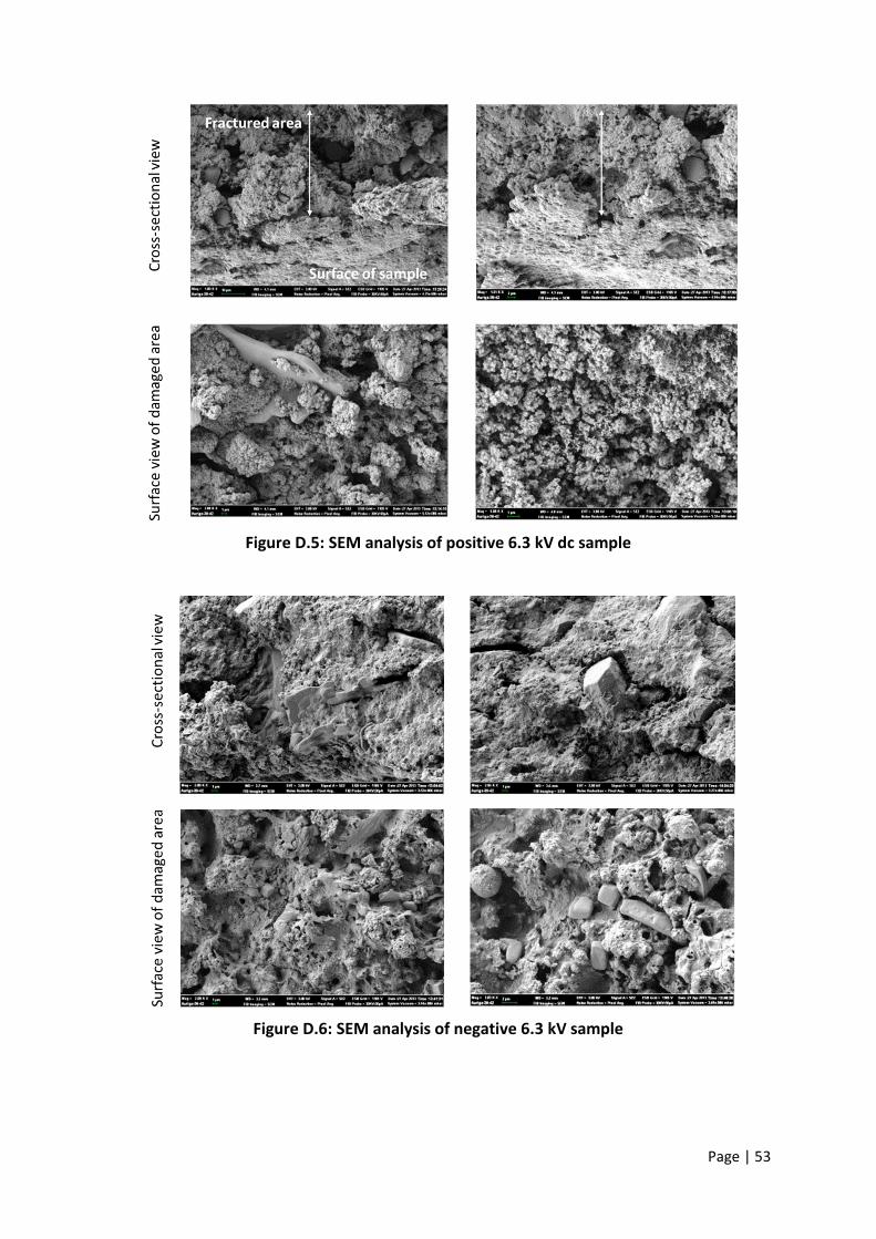
In the positive dc test at 4.5 kV only 3 samples were energised. After 5 minutes scintillations were observed to be more vigorous than the ac test, and after 15 minutes tracks were visible along the entire length from the HV to the ground electrode. After approximately 40 minutes sample 2 (test position (TP) 2) showed serious erosion and evidence of a hole being burnt into the material at the ground electrode, shown in Figure 8.
(a) (b)
Figure 8: (a) Burning on sample 2 at ground electrode and; (b) erosion noted on sample 2
Page | 8
The test was finally stopped after 95 minutes. Figure 9 shows the samples after testing. The maximum (1 minute max) current recorded (on sample 3, tp1) after 65 minutes was 75 mA, with an average of 47.6 mA.
Figure 9: All three samples showing signs of severe erosion
Negative dc test at 4.5 kV
In the negative dc test at 4.5 kV, it was observed that an arc root had formed on sample 2 after 5 minutes, and aggressive erosion began after 20 minutes, shown in Figure 10.
(a) (b)
Figure 10: (a) Formation of the arc root, and (b) the starting of erosion.
Approximately 42 minutes after the test had started, the arcing had caused erosion from the lower electrode to the upper one, as shown in Figure 11.
Page | 9
Figure 11: Severe erosion on sample 2 after 42 minutes
The other samples were still energised to evaluate the various stages of erosion and the test was eventually stopped 112 minutes after voltage application. A one-minute maximum current was recorded periodically for the duration of the test (on sample 1, TP 1). The average current recorded was 27.3 mA, with a maximum of 50 mA being observed.
Materials Analysis
(a) (b)
Figure 12: Cross-sectional views of (a) +4.5 kV dc and (b) -4.5 kV dc
Page | 10
(a) (b)
Figure 13: FTIR comparisons between (a) +4.5 kV dc (pink) and (b) -4.5 kV dc (blue) against the control (green)
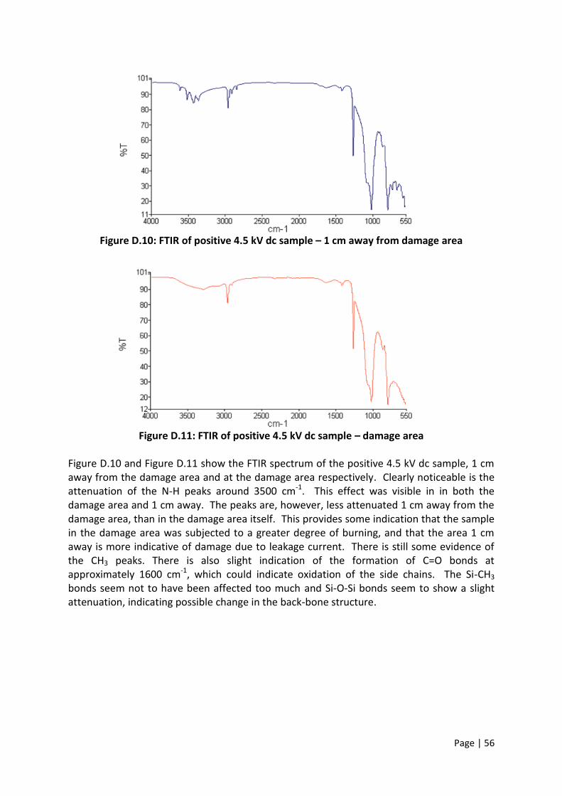
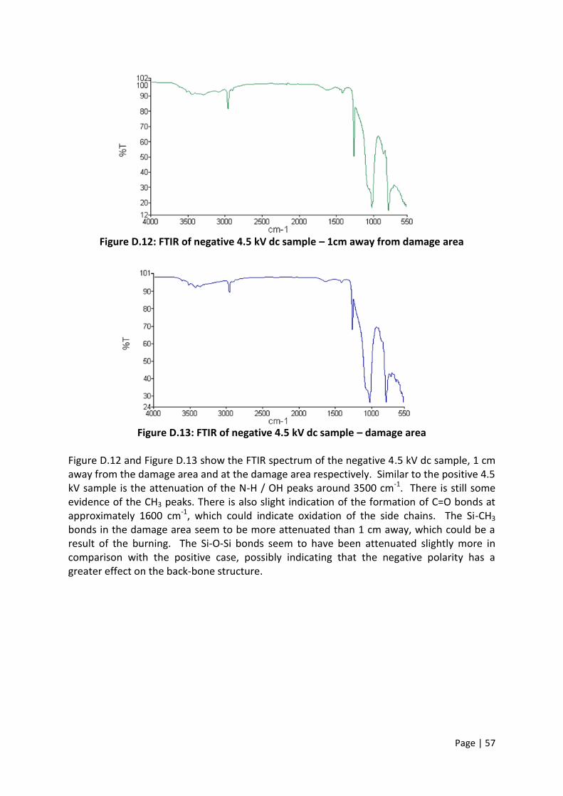
Figure 12 shows a segregated texture induced by the dc energistaion in both positive and negative cases. The regular occurrence of large inclusions gives the positive sample a courser appearance than the negative. The FTIR spectra in Figure 13 shows an attenuation of the N-H peaks around 3500 w/n in both positive and negative samples. However, there are no visible differences from the control spectra at around 1200-1500, but the disappearance of peaks around 2800 is noted.
5.3 Positive and negative dc test: 6.3 kV
It was observed that in the positive dc test a localised arc spot developed on sample 2 (TP2) after only 17 minutes, while the other two samples developed arc spots a few minutes later. Approximately 30 minutes into the test saw the beginning of erosion on sample 2, shown in Figure 14, and 10 minutes later small flames were noted.
(a) (b)
Figure 14: (a) Arcing and the starting of erosion in sample 2, and (b) small flames observed after 40 minutes
Page | 11
The test was stopped after 58 minutes, with sample 2 having been burnt all the way through, shown in Figure 15.
(a) (b)
Figure 15: (a) Sample 2 burnt all the way through, and (b) all 3 samples after the test.
The maximum current recorded after 50 minutes was 100 mA, while the average current over the test duration was 50.6 mA.
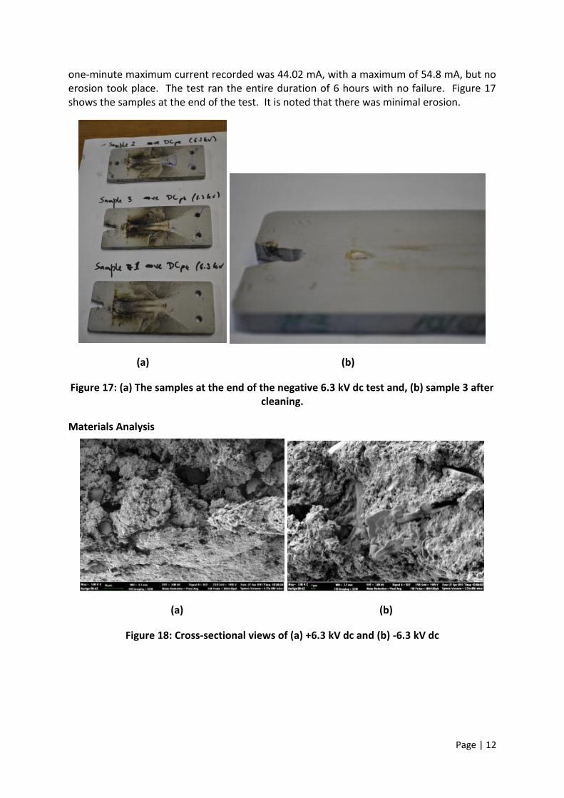
Negative dc test at 6.3 kV
For the negative dc test at 6.3 kV it was observed that while there were arc roots developed, as in the previous tests, aggressive erosion was not prevalent as in the negative 4.5 kV dc case. Visually, there were more scintillations across the surface of the samples, shown in Figure 16.
Figure 16: Development of arc roots with scintillations across the sample surface
It was also observed that the contaminant was evaporated almost instantaneously as soon as it approached the ground electrode. In all the previous tests there was wetting observed at the base of the stands, whereas in this test the bases were relatively dry. The average
Page | 12
one-minute maximum current recorded was 44.02 mA, with a maximum of 54.8 mA, but no erosion took place. The test ran the entire duration of 6 hours with no failure. Figure 17 shows the samples at the end of the test. It is noted that there was minimal erosion.
(a) (b)
Figure 17: (a) The samples at the end of the negative 6.3 kV dc test and, (b) sample 3 after cleaning.
Materials Analysis
(a) (b)
Figure 18: Cross-sectional views of (a) +6.3 kV dc and (b) -6.3 kV dc
Page | 13
(a) (b)
Figure 19: FTIR comparisons between (a) +6.3 kV dc (orange) and (b) -6.3 kV dc (blue) against the control (green)
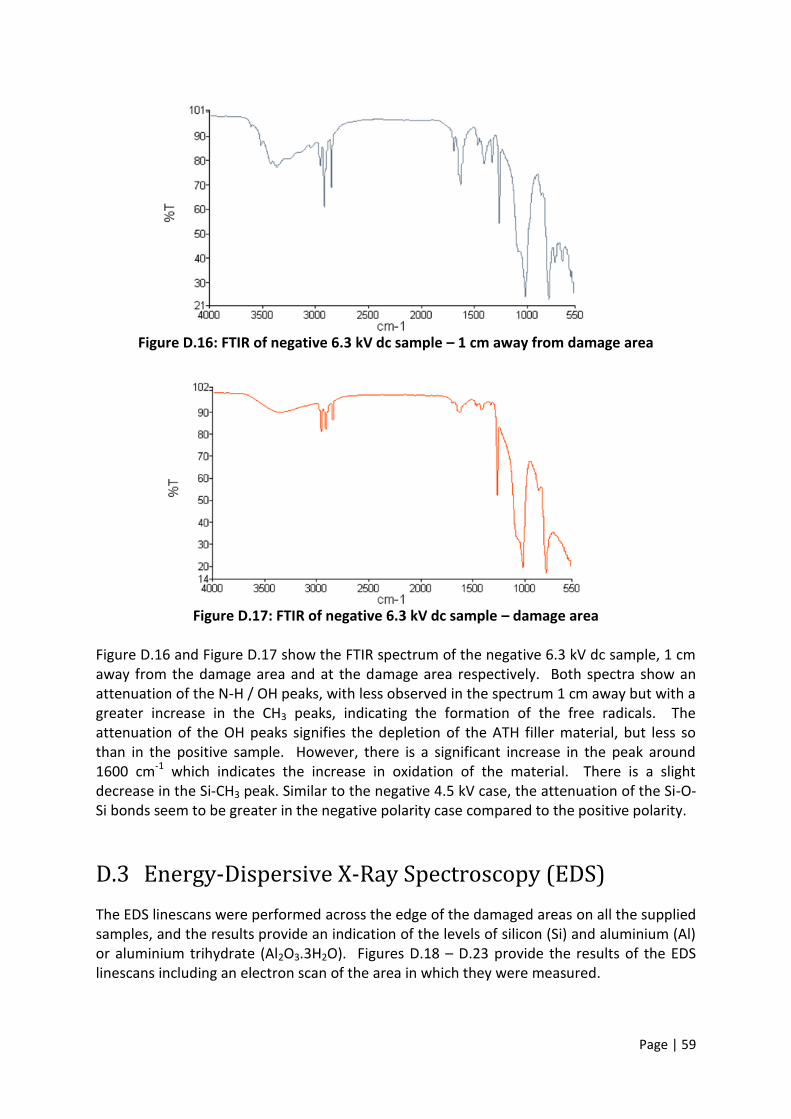
Both the positive and negative samples show a segregated texture, as can be seen in Figure 18, however, the segregation appears to be finer in the positive case. When compared against the control sample, the FTIR spectra for both the positive and negative samples indicate an attenuation of the peaks around 3500 w/n, shown in Figure 19. In contrast, the peaks between 1200 and 1500 w/n became more pronounced in both positive and negative, when compared to the control sample.
6 Conclusions and recommendations
A HTV silicone rubber material was successfully tested with the inclined plane test method, using three voltage types: ac, positive dc and negative dc. The test voltages used were 4.5 kV rms for ac, 4.5 kV and 6.3 kV for both positive and negative dc. Materials analyses using SEM, EDS, FTIR and XRD were also conducted.
A summary of all the IPT testing results is presented in Table 1.
Page | 14
Table 1: Summary of all the IPT tests
AC Test ran for 6 hours with minimal erosion.
Positive 4.5 kV dc
40 minutes after voltage application – serious erosion
55 min – erosion from ground electrode to HV electrode
75 min – flames noticed on sample 2
95 min – test stopped
Average current – 47.6 mA
Max current – 75 mA
Positive 6.3 kV dc
17 min–arc spot developed on sample 2
30 min – erosion began on sample 2
40 min – flames on sample 2
58 min – test stopped, sample 2 burnt
Average current – 50.6 mA
Max current – 100 mA
Negative 4.5 kV dc
5 min– arc roots developed on sample 2
20 min – severe erosion
42 min – erosion progressed from ground electrode to HV electrode
112 min – test stopped
Average current – 27.3 mA
Max current – 50 mA
Negative 6.3 kV dc
Arc roots seem to develop, with minimal erosion, and test ran for 6 hours
Average current – 44.02 mA
Max current – 54.8 mA
Page | 15
The samples of the ac test showed minimal erosion of negligible depth and ran for the full duration of 6 hours.
The samples of the 4.5 kV positive dc ran for 95 minutes, while the 6.3 kV dc test ran for 58 minutes before being stopped. It is noticed that the average one-minute maximum currents for both the tests were similar and displayed high peak magnitudes as compared to the other tests. In both tests, samples displayed severe erosion. This could possibly be attributed to the high peak current magnitudes observed.
The samples of the negative 4.5 kV dc test developed severe erosion after 20 minutes, which is less than the positive case. The average one-minute maximum current observed for this test was less than in the positive dc case, as was the maximum peak current magnitude.
The samples of the negative 6.3 kV case, which were expected to fail in a similar manner and time as the negative 4.5 kV test, ran for the full 6 hours and showed minimal erosion of negligible depth. The erosion appeared similar to the ac case, although the track marks were more distinct and showed greater surface blackening. The rapid evaporation of contaminant prior to reaching the ground electrode, limits the current flowing on the surface of the sample. This would result in considerably less energy in the discharges and less damage to the insulation.
All experimental samples were examined both at the interface between damaged and
undamaged areas to reveal the marked contrast in structure, as well as within the crater
formed by the discharge. There was a discolouration of the area immediately around the
damaged area that with the naked eye did not appear to extend beyond 0.5 mm into the
sample. Preliminary EDS line scans across cross sections of some discharge-damaged
samples showed that the concentration of aluminium and silicon decreased markedly in the
area immediately surrounding the damage crater. There is an occasional spike of chlorine in
the same area, but was not consistent across all samples. FTIR shows marked differences
between the damaged/burnt and virgin areas as expected. Evident in the dc energised
samples is the attenuation of the peaks in the 3600 to 3300 wave number range.
It is concluded that for the dc voltages investigated, especially the positive polarity, a
stronger erosive effect on the silicone rubber material was observed, when compared to ac.
This is supported by the positive dc cases exhibiting higher average and maximum leakage
currents than the negative cases. Also noted in the positive dc samples, was the greater
degree of attenuation of the –OH bonds, indicating depletion of the filler material as a
results of leakage current and discharge activity. It is postulated in the negative dc case, the
lower currents result in more damage, possibly due to the fact that the higher currents do
not form stable arc roots at the ground electrode, and therefore do not initiate the severe
erosion observed in the 4.5 kV dc case. Both positive and negative samples show
attenuation of the Si-O bonds indicating some degree of damage / modification to the
backbone structure, which means permanent structural change to the material.
Page | 16
7 References
[1] Handbook on Modern HVDC Power Transmission, Eskom Power Series, Volume 9, unpublished.
[2] IEC 60587:2007(E), “Electrical Insulating Materials Used Under Severe Ambient Conditions – Test Methods for Evaluating Resistance to Tracking and Erosion” Third Edition, 2007.
[3] J.M. Seifert, D. Stefanini, H. Janssen, “HTV Silicone Composite Insulators for HVDC Applications – Long Term Experience with Material and Design for 500 kV and Above”, 16th International Symposium on High Voltage Engineering, Cape Town, 2009.
[4] G. Heger, H.J. Vermeulen, W.L. Vosloo, “Evaluation of the Performance of HTV Silicone Rubber Exposed to AC & DC Surface Discharges Using the Inclined Plane Test”, 16th International Symposium on High Voltage Engineering, Cape Town, 2009.
Page | 17
Appendix A: Literature Review
This section is a summary of the literature that was reviewed in the compiling of this
dissertation.
A.1 Review of Literature
The work conducted by Baharom et al [1] reported that the silicone layer used as the
housing of high voltage insulators provides a hydrophobic characteristic which may assist in
the reduction of dry bands occurring on the surface. Even when this characteristic is
temporarily lost due to atmospheric conditions or temporary discharge activity, silicone
rubber materials have the capability of recovering their hydrophobicity after a certain
period. When compared with epoxy resins, silicone rubbers filled with alumina trihydrate
(ATH) are shown to have a good capability in suppressing or delaying tracking and erosion
on the surface. The research described the relative performance of pure composite, silicone
rubber and silicone rubber coated composite samples during inclined plane testing. The
correlation between visual observations of damage and the leakage current behaviours of
the specimens under constant ac stresses were investigated. The thermal stresses during
the tracking of the samples were also analysed. The inclined plane test setup utilised
accommodated up to five samples simultaneously. The samples were all subjected to a
constant voltage tracking test, and 2.5 kV ac voltage stress was applied to each of the
samples. The overcurrent protection operated when the current exceeded 60 mA for 2 to 3
seconds. The fail criterion was the point at which the overcurrent protection operated. In
terms of the time to failure, the composite samples had the shortest time to failure of less
than 1 hour. The arcs that developed on the surface rapidly carbonised the surface, therby
protecting it from further damage, however the carbonisation increased the electric field
across the remainder of the sample surface increasing the likelihood of failure. The pure
silicone samples survived for over 20 hours without failure. A more significant level of
erosion occurred, but there was no carbonisation seen. For the silicone coated composite
samples, the time to failure increased as the thickness of the coating was increased. The
leakage current waveforms observed showed no direct correlation with surface
temperatures, and no significant analysis of the leakage current were done.
The research conducted by Heger et al [2] considered the erosion performance of a HTV
silicone rubber based insulator material using the Incline Plane Test method. AC, positive dc
and negative dc of 4 kV rms were applied to the samples. The samples were then evaluated
according to visual observations, erosion depth, erosion area and sample mass loss.
Leakage current measurements were also measured. The test voltage was set at 4 kV rms
based on previous studies, and the contaminant conductivity was selected as 2.5 mS/cm.
On ac application the samples showed minimal erosion and discolorations observed were
Page | 18
superficial. Positive dc voltage showed massive erosion, with deep cavities forming almost
halfway along the sample length. A large degree of chalking was observed as was
permanent discolouration. The samples in the negative dc test showed greater erosion than
the ac test, but not as much as the positive dc test. Some degree of chalking was observed.
Discolorations observed were superficial. The positive dc sample showed a far higher mass
loss compared to the other two test voltages, but with a high degree of variation. The
positive dc tests also showed the highest rms leakage current. The ac test showed higher
hourly leakage currents than the negative dc tests, but the negative test showed greater
erosion severity.
The publication by Seifert et al [3] presented a design review of exiting installations with
HVDC silicone rubber composite insulators over 30 years. In addition the electrical
performance and material ageing characteristics were reviewed through the tracking and
erosion tests conducted using the IEC 60587 (Incline Plane Test) at dc voltage stress, as well
as those of a 5000 hour multi-stress test at dc voltage. Seifert et al found that the long-term
experience with existing silicone rubber composite insulators in HVDC overhead lines was
excellent. This was supported by evidence found in the service experience of the Cahora
Bassa – Apollo and Pacific Intertie HVDC transmission lines insulated with silicone rubber
insulators for more than 25 years. In the 5000 hour multi-stress test performed with dc
voltage, the leakage currents observed were much lower than the comparable ac test. The
hydrophobicity of the silicone rubber material was maintained throughout the test period
and no damage was found due to tracking and erosion. This supported their long-term
service experience. The incline plane test was conducted with a variation of dc voltages of
both polarities, from 2.5 kV to 5.5 kV. These were compared with a series of ac tests. The
material used was a HTV silicone rubber with a 58% ATH filler. For the positive dc test the
depth and length of erosion was found to increase with increasing voltage, with a doubling
of both observed in the increase from 4.5 kV to 5.5 kV. For the negative dc stress a clear
tendency could not be established, although the severity of depth and length was high.
Both polarities were much higher than the ac test, and in the ac tests the samples
performed as expected. The conclusion was that the test erosion severities at both dc
polarities are significantly higher than those at ac, but cautioned that if ac material tests are
applied for dc voltages, the results may be misleading and not transferable to real insulator
applications.
Gorur et al [4] presented a hypothesis for dry band arcing in silicone rubber material used
for outdoor insulation, and experimentally tried to prove the hypothesis. They predicted
permanent changes in the material and utilised analytical methods such as FTIR, XRD, EDX
and surface roughness measurements to study the changes. The aspect of ageing
considered in the work was that resulting from dry band arcing. In order to prove the
hypothesis, experimental investigation of new and aged material was performed in a fog
chamber. The samples that were used for the testing were silicone rubber coatings over
porcelain rods and silicone rubber elastomer rods. The samples were subjected to a dc
Page | 19
electrical stress of 40 V/mm and conductivity of 1000 to 2000 µS/cm. The samples were
subjected to both the fog and voltage for continuous 8 hours, and thereafter a 16 hour rest
period for hydrophobicity recovery. The total duration of exposure for the samples was
varied to provide various degrees of ageing. Contact angle measurements were performed
on the samples after the fog chamber tests, and very similar results were found between
the aged and new samples. This indicated that the aged samples had recovered their
hydrophobicity. The EDX results, which give the ratio of silicone to aluminium, showed a
depletion of the low molecular weight (LMW) polymer chains on the top surface layers,
which Gorur et al felt proved their hypothesis. The surface roughness measurements
indicated that the aged sample surfaces were at least 3 times as rough as the virgin sample.
The FTIR results showed that there was a reduction of all the chemical groups of the silicone
polymer due to the ageing. The XRD results indicated that the silicone polymer had become
more crystalline with ageing, and the size of the filler materials has also increased. All of the
results supported the hypothesis that the dry band arcing had caused permanent changes to
the structure of the material.
Chandrasekar et al [5] also studied the tracking phenomenon in silicone rubber material
under ac and dc voltages. They considered the influence of the applied voltage magnitude,
conductivity and flow rate of the contaminant on tracking. The testing was carried out using
the Incline Plane Test method, and the ac and dc voltages were fixed at 4.5 kV and 4 kV
respectively. It was observed that the silicone rubber with ATH filler, performed well under
ac voltage application. Under the dc voltages, irrespective of polarity, it was found that the
silicone rubber failed due to tracking, and the tracking time was less under negative dc as
compared to the positive dc. It was also found that the magnitude of leakage current flow
under negative dc was higher than that under positive dc voltage.
In the study conducted by Kim et al [6] they considered RTV coatings subjected
simultaneously to salt fog and electrical stress. Attenuated total reflected FTIR and electron
spectroscopy for chemical analysis (ESCA) were employed to investigate chemical changes in
the materials. The RTV coating were applied to fibreglass reinforced plastic rods and were
exposed to 10 hours of salt fog, while simultaneously being subjected to an ac stress of 14.4
kV. The results of the FTIR and ESCA indicted that silicone fluid was formed both on the
surface and in the bulk of the exposed materials as a result of the heat generated during dry
band arcing. The heat thus produced caused hydrolysis, scission and interchange of the
siloxane bonds. The significant changes noticed on the surface of the materials was the
decrease in the CH3 groups and the increased oxygen in the Si-O bonding due to oxidation
caused by the dry band arcing. The increase in oxygen also led to the rapid decrease in the
hydrophobicity during the dry band activity.
The work conducted by Liu et al [7] was on a high voltage composite insulator that showed
sever degradation and failure of the silicone elastomer shed following service in a sub-
station environment. The extent of damage of the silicone elastomer was quantified
Page | 20
through the use of several chemical analysis techniques. Liu et al found that on some parts
of the elastomer the degradation was so severe that the shed crumbled away, while on
other parts the damage was less severe. The explanation offered was the variation in the
electric field along the insulator, and it was surmised that due to the environmental
conditions the electric field strength on and around the insulator reached the corona onset
threshold on parts of the elastomer surface. This led to the loss of hydrophobicity in those
regions, and over time led to the degradation of the material. The SEM analysis revealed
the cracks and pits in the surface, as well as the decrease in the polymer content due to less
of the polymer matrix being present. The x-ray photoelectron spectroscopy (XPS) provided
an indication of the silicone to aluminium ratio and showed that the surface experienced
more degradation than the inner bulk, due to the extensive surface electrical and thermal
activity (most likely dry-band arcing). The thermogravimetric analysis (TGA) indicated ATH
dehydration weight loss and weight loss caused by the decomposition of the remaining
polymer material.
Experiments were carried out by Haddad et al [8] on samples collected from a 22 kV silicone
rubber insulator. Results from aged specimens were compared against a new sample and
an electrically damaged sample. The damaged sample was created by artificially polluting a
new sample with salt and distilled water, and placing the sample between two electrodes
energised with high voltage ac. Flashover was produced between the electrodes and the
process was repeated fifty times to ensure degradation of the sample. All of the samples
were then subjected to accelerated ageing using an Accelerated Weathering Tester at 50°C
and UVA exposure of 340nm at an irradiation intensity of 0.68 W/m2 for up to 3000 hours.
The degradation was examined using SEM and FTIR. The SEM analysis revealed that the
new samples have a smooth, more homogenous and less porous surface while the surface
roughness and porosity increased with ageing for the aged silicone rubber insulator. The
FTIR analysis showed the disappearance of the ATH filler in the damaged samples due to the
effect of arcing, flashover and pollution.
Ganga et al [9] carried out FTIR, EDAX and SEM analyses on two different silicone rubber
formulations subjected to the Incline Plane Test (IPT) for both with and without UV radiation
of different intensities. The SEM analysis for both formulations indicated a greater degree
of surface damage for samples exposed to UV and IPT, than samples subjected to IPT alone,
implying that UV plays a dominant role in the degradation. The EDAX showed that the
depletion of aluminium was also greater for samples tested with UV superimposed during
the IPT. It was also inferred that the intensity of the UV radiation during the IPT and long
exposure to UV played a major role in the deterioration of the surface characteristics of the
samples. The other elements did not show a significant change except for silicone and
oxygen, when compared to the virgin sample. The FTIR carried out on both formulations
clearly showed that the breakage of the Si-O bond was higher in samples exposed to UV.
Page | 21
Kuroyagi et al [10] conducted a study on the degradation and characteristics of leakage
current on silicone rubber under positive dc and ac voltage using the Rotating Wheel Dip
Test (IEC 1302:1995). The analysis was performed by periodically observing the magnitude
of leakage current, surface appearance and weight loss. After 1000 hours of testing no
tracking was observed on the surface of the samples with either ac or positive dc stress.
However, deep erosion in limited areas near the electrodes was noticed on the samples in
the dc test. On the ac samples the erosion was less severe but covered a larger area. This
was attributed to the partial discharges near the ground electrode being more active in the
ac test, but the dc voltage created deeper damage in a smaller area. Kuroyagi et al noted
that at higher electrical stress above 50 V/mm the surface degradation was severe,
especially the erosion under positive dc voltage. It was stated that the degradation could be
suppressed if the stress was kept below 25 V/mm, which the researchers felt was more in
line with actual electrical stress experienced by transmission line insulators.
Bruce et al [11] conducted Incline Plane Tests on three formulations of silicone rubber, and
the materials were tested under three voltage levels of 2.3 kV, 2.7 kV and 3.2 kV for both
positive and negative dc. It was found that one of the formulations exhibited the lowest
mass loss due to erosion and erosion depth, thus it was postulated that different material
properties may affect the electrical stress such that the nature of the surface discharges
change. In the dc tests it was found that there was evidence of erosion of the positive
electrode from electrolysis and oxidation of the bottom electrode due to high temperature
arcing. The results also showed a clear difference between the positive and negative dc test
conditions. The positive dc tests had higher average leakage currents, were more
intermittent and seemed to produce deeper erosion than the negative tests.
A.2 References
[1] M.N.R. Baharom and I. Cotton, “Inclined Plane Tests of Composite, Silicone Rubber
and Composite Silicone Rubber Coated Materials”, 16th International Symposium on
High Voltage Engineering (ISH), Cape Town, South Africa, August 2009.
[2] G. Heger, H.J. Vermeulen and W.L. Vosloo, “Evaluation of the Performance of HTV
Silicone Rubber Exposed to AC and DC Surface Discharges using the Incline Plane
Test”, 16th International Symposium on High Voltage Engineering (ISH), Cape Town,
South Africa, August 2009.
[3] J.M. Seifert, D. Stefanini and H. Janssen, “HTV Silicone Composite Insulators for
HVDC Applications – Long-term Experience with Material and Design for 500 kV and
Above”, 16th International Symposium on High Voltage Engineering (ISH), Cape
Town, South Africa, August 2009.
Page | 22
[4] R.S. Gorur, G.G. Karady, A. Jagota, M. Shah and A.M. Yates, “Aging in Silicone Rubber
Used for Outdoor Insulation”, IEEE Transactions on Power Delivery, Vol. 7, No. 2,
April 1992.
[5] S. Chandrasekar, R. Sarathi and M.G. Danikas, “Analysis of Surface Degradation of
Silicone Rubber Insulation Due to Tracking Under Different Voltage Profiles”,
[11] G.P. Bruce, S.M. Rowland and A. Krivda, “Performance of Silicone Rubber in DC
Inclined Plane Tracking Tests”, IEEE Transactions on Dielectrics and Electrical
Insulation, Vol. 17, No. 2, April 2010.
Page | 23
Appendix B: Measuring Equipment & Test
Methodology
This section describes the various methods and techniques used for the testing and analysis
of the silicone rubber samples.
B.1 Incline Plane Test
This test method is specified in the international standard IEC 60587: 2007 “Electrical
Insulating Materials Used Under Severe Ambient Conditions – Test Methods for Evaluating
Resistance to Tracking and Erosion” [1]. This standard describes two test methods for the
evaluation of electrical insulating materials for use under severe ambient conditions under
power frequency (45 Hz – 65 Hz) by measurement of the resistance to tracking and erosion
resistance, using a liquid contaminant and inclined plane specimens. The two methods are:
- Method 1: Constant tracking voltage
- Method 2: Stepwise tracking voltage
The method employed for the purposes of this research was the method 1, constant
tracking voltage.
The dielectric sample under test is placed on a 45 degree angle and a contaminant made
from deionised water, ammonium chloride and a soaping agent Triton X-100
(isooctylphenoxypolyethoxyethanol, [(C14H22O(C2H4O)n); n=9-10]) drips down the underside
of the sample between two electrodes energised with a specified voltage [2]. This is shown
in Figure B.1. The contaminant emerges from a hole in the top electrode, via a peristaltic
pump, and flows down the surface of the sample to the bottom (grounded) electrode, which
has a series of teeth to permit the passage of contaminant without damming up. The
required conductivity of the contaminant, according to IEC 60587, should be 2.53 mS/cm.
The conductivity used for all the tests in this study was 2.7 mS/cm. Experiments conducted
by Seifert et al [3] showed maximum erosion with a contaminant conductivity of 2.5 mS/cm
at 5.5 kV. Figure B.2 shows the actual test setup used for this research.
Page | 24
Figure B.1: Assembly of the electrodes – contaminant flows from top to bottom
Figure B.2: Actual incline plane test setup used for this study
Page | 25
For the positive dc tests a Spellman 50 kV dc, 80 mA stand-alone supply was used to charge a smoothing capacitor of 66 µF coupled to the necessary peripheral equipment for protection and switching, shown in Figure B.3. The tests voltages used were 4.5 kV and 6.3 kV. For the negative dc tests a half wave rectifier circuit was constructed. This setup used an 80 kV (peak inverse voltage), 500 mA diode arrangement in series with a 100 Ω resistor. This was then used to charge the 66 µF capacitor, and coupled to the necessary peripheral equipment, shown in Figure B.4. The test voltages were selected as 4.5 kV and 6.3 kV. The test configuration used for the ac tests was the same as for the positive dc (Figure B.3) with the exclusion of the Spellman dc supply. The ac was supplied through a 230 V / 12 kV single phase step-up transformer.
Figure B.3: Circuit diagram for positive dc setup
Figure B.4: Circuit diagram for negative dc setup
For the ac and dc tests, visual observations, photo and video recordings were conducted,
using a Nikon D90 SLR digital camera and Sony Digital video camera respectively. Infra-red
and daylight ultra-violet observations and recording were captured utilising an Eskom/CSIR
Multi Spectral camera, while night ultra-violet observations were done using a night corona
camera - CSIR CC1. In addition, for the dc tests, a Fluke 289 digital multi-meter was
connected in series with sample 1 (in test position 1 – test positions were numbered from 1-
5 from right to left) to measure the leakage current. The current was manually recorded at
periodic intervals throughout the tests.
Spellman DC
Supply +ve
Incline Plane
Test Chamber
ac 230V C1 C2
33µF 33µF
HV Switch n/o
R1 3Ω
Test Transformer
Incline Plane
Test Chamber
ac 230V C1 C2
33µF 33µF
HV Switch n/o
R2 3Ω
80kV PIV
D1 R1 100Ω
Page | 26
B.2 Scanning Electron Microscopy (SEM)
A scanning electron microscope (SEM) is a type of electron microscope that produces
images of a sample by scanning it with a focused beam of electrons. The electrons interact
with atoms in the sample, producing various signals that can be detected and that contain
information about the sample's surface topography and composition. The electron beam is
generally scanned in a raster scan pattern, and the beam's position is combined with the
detected signal to produce an image. SEM can achieve resolution better than 1 nanometer.
Specimens can be observed in high vacuum, in low vacuum, and (in environmental SEM) in
wet conditions. The most common mode of detection is by secondary electrons emitted by
atoms excited by the electron beam. The number of secondary electrons is a function of the
angle between the surface and the beam. On a flat surface, the plume of secondary
electrons is mostly contained by the sample, but on a tilted surface, the plume is partially
exposed and more electrons are emitted [4]. By scanning the sample and detecting the
secondary electrons, an image displaying the tilt of the surface is created. Figure B.5 shows
a typical scanning electron microscope, similar to the one used at the CSIR for the purposes
of the analysis of the silicone rubbers samples in this study.
Figure B.5: Typical scanning electron microscope
The types of signals produced by a SEM include secondary electrons (SE), back-scattered
electrons (BSE), characteristic X-rays, light (cathodoluminescence) (CL), specimen current
and transmitted electrons. Secondary electron detectors are standard equipment in all
SEMs, but it is rare that a single machine would have detectors for all possible signals. The
signals result from interactions of the electron beam with atoms at or near the surface of
the sample. In the most common or standard detection mode, secondary electron imaging
or SEI, the SEM can produce very high-resolution images of a sample surface, revealing
details less than 1 nm in size. Due to the very narrow electron beam, SEM micrographs have
a large depth of field yielding a characteristic three-dimensional appearance useful for
Page | 27
understanding the surface structure of a sample. This is exemplified by the micrograph of
pollen shown above. A wide range of magnifications is possible, from about 10 times (about
equivalent to that of a powerful hand-lens) to more than 500,000 times, about 250 times
the magnification limit of the best light microscopes.
All samples must also be of an appropriate size to fit in the specimen chamber and are
generally mounted rigidly on a specimen holder called a specimen stub. Several models of
SEM can examine any part of a 6-inch (15 cm) semiconductor wafer, and some can tilt an
object of that size to 45°. For conventional imaging in the SEM, specimens must be
electrically conductive, at least at the surface, and electrically grounded to prevent the
accumulation of electrostatic charge at the surface. Metal objects require little special
preparation for SEM except for cleaning and mounting on a specimen stub. Nonconductive
specimens tend to charge when scanned by the electron beam, and especially in secondary
electron imaging mode, this causes scanning faults and other image artefacts. They are
therefore usually coated with an ultrathin coating of electrically conducting material,
deposited on the sample either by low-vacuum sputter coating or by high-vacuum
evaporation. Conductive materials in current use for specimen coating include gold,
gold/palladium alloy, platinum, osmium, iridium, tungsten, chromium and graphite. In the
case of the silicone rubber samples, the specimens were rendered conductive using
sputtered gold.
In a typical SEM, an electron beam is thermionically emitted from an electron gun fitted
with a tungsten filament cathode. Tungsten is normally used in thermionic electron guns
because it has the highest melting point and lowest vapour pressure of all metals, thereby
allowing it to be heated for electron emission, and because of its low cost. The electron
beam, which typically has an energy ranging from 0.2 keV to 40 keV, is focused by one or
two condenser lenses to a spot about 0.4 nm to 5 nm in diameter. The beam passes through
pairs of scanning coils or pairs of deflector plates in the electron column, typically in the
final lens, which deflect the beam in the x and y axes so that it scans in a raster fashion over
a rectangular area of the sample surface. When the primary electron beam interacts with
the sample, the electrons lose energy by repeated random scattering and absorption within
a teardrop-shaped volume of the specimen known as the interaction volume, which extends
from less than 100 nm to approximately 5 μm into the surface. The size of the interaction
volume depends on the electron's landing energy, the atomic number of the specimen and
the specimen's density. The energy exchange between the electron beam and the sample
results in the reflection of high-energy electrons by elastic scattering, emission of secondary
electrons by inelastic scattering and the emission of electromagnetic radiation, each of
which can be detected by specialized detectors. The beam current absorbed by the
specimen can also be detected and used to create images of the distribution of specimen
current. Electronic amplifiers of various types are used to amplify the signals, which are
displayed as variations in brightness on a computer monitor. Each pixel of computer video
memory is synchronized with the position of the beam on the specimen in the microscope,
Page | 28
and the resulting image is therefore a distribution map of the intensity of the signal being
emitted from the scanned area of the specimen. Figure B.6 shows a schematic diagram of a
SEM. Figure B.7 shows a SEM image of the control sample of the silicone rubber material
used for the incline pane testing, with varying magnifications.
Figure B.6: Schematic diagram of a SEM
Figure B.7: SEM images of the silicone rubber control sample
Fourier transform infrared spectroscopy (FTIR) is a technique which is used to obtain an infrared spectrum of absorption, emission, photoconductivity or Raman scattering of a solid, liquid or gas. An FTIR spectrometer simultaneously collects spectral data in a wide spectral range. This confers a significant advantage over a dispersive spectrometer which measures intensity over a narrow range of wavelengths at a time [5]. The term Fourier transform infrared spectroscopy originates from the fact that a Fourier transform (a mathematical process) is required to convert the raw data into the actual spectrum. Fourier transform spectroscopy shines a beam containing many frequencies of light at once, and measures how much of that beam is absorbed by the sample. Next, the beam is modified to contain a different combination of frequencies, giving a second data point. This process is repeated many times. Afterwards, a computer takes all these data and works backwards to infer what the absorption is at each wavelength. The beam described is generated by starting with a broadband light source - one containing the full spectrum of wavelengths to be measured. The light shines into a Michelson interferometer - a certain configuration of mirrors, one of which is moved by a motor. As this mirror moves, each wavelength of light in the beam is periodically blocked, transmitted, blocked, transmitted, by the interferometer, due to wave interference. Different wavelengths are modulated at different rates, so that at each moment, the beam coming out of the interferometer has a different spectrum. Computer processing is required to turn the raw data (light absorption for each mirror position) into the desired result (light absorption for each wavelength). The processing required turns out to be a common algorithm called the Fourier transform (hence the name, "Fourier transform spectroscopy"). The raw data is sometimes called an "interferogram". Figure B.8 shows a schematic diagram of a Michelcon interferometer, configured for FTIR. Figure B.9 shows the FTIR spectrum obtained for the control sample of silicone rubber used in the Incline Plane Test showing the absorption peaks of the constituents.
Page | 30
Figure B.8: Schematic diagram of a Michelson interferometer, configured for FTIR
Figure B.9: FTIR spectrum of the control sample of HTV silicone rubber
Page | 31
B.4 Energy Dispersive X-Ray Spectroscopy (EDS)
Energy-dispersive X-ray spectroscopy (EDS, EDX, or EXDS), sometimes called energy
dispersive X-ray analysis (EDXA) or energy dispersive X-ray microanalysis (EDXMA), is an
analytical technique used for the elemental analysis or chemical characterization of a
sample. It relies on an interaction of some source of X-ray excitation and a sample. Its
characterization capabilities are due in large part to the fundamental principle that each
element has a unique atomic structure allowing unique set of peaks on its X-ray spectrum.
To stimulate the emission of characteristic X-rays from a specimen, a high-energy beam of
charged particles such as electrons or protons (see PIXE), or a beam of X-rays, is focused into
the sample being studied. At rest, an atom within the sample contains ground state (or
unexcited) electrons in discrete energy levels or electron shells bound to the nucleus. The
incident beam may excite an electron in an inner shell, ejecting it from the shell while
creating an electron hole where the electron was. An electron from an outer, higher-energy
shell then fills the hole, and the difference in energy between the higher-energy shell and
the lower energy shell may be released in the form of an X-ray. The number and energy of
the X-rays emitted from a specimen can be measured by an energy-dispersive spectrometer.
As the energy of the X-rays are characteristic of the difference in energy between the two
shells, and of the atomic structure of the element from which they were emitted, this allows
the elemental composition of the specimen to be measured [6].
Four primary components of the EDS setup are:
1. the excitation source (electron beam or x-ray beam)
2. the X-ray detector
3. the pulse processor
4. the analyser.
Electron beam excitation is used in electron microscopes, scanning electron microscopes
(SEM) and scanning transmission electron microscopes (STEM). X-ray beam excitation is
used in X-ray fluorescence (XRF) spectrometers. A detector is used to convert X-ray energy
into voltage signals; this information is sent to a pulse processor, which measures the signals
and passes them onto an analyser for data display and analysis. The most common detector
now is Si(Li) detector cooled to cryogenic temperatures with liquid nitrogen; however newer
systems are often equipped with silicon drift detectors (SDD) with Peltier cooling systems.
Figure B.10 shows an EDS scan of the silicone rubber control sample used for the Incline
Plane Test.
Page | 32
Figure B.10: EDS scan of the silicone rubber control sample used for the IPT tests
B.5 References
[1] IEC 60587:2007(E), “Electrical Insulating Materials Used Under Severe Ambient
Conditions – Test Methods for Evaluating Resistance to Tracking and Erosion”, Third
Edition, 2007.
[2] G.P. Bruce, S.M. Rowland and A. Krivda, “Performance of Silicone Rubber in DC
Inclined Plane Tracking Tests”, IEEE Transactions on Dielectrics and Electrical
Insulation, Vol. 17, No. 2, April 2010.
[3] J.M. Seifert, D. Stefanini and H. Janssen, “HTV Silicone Composite Insulators for
HVDC Applications – Long Term Experience with Material and Design for 500 kV and
Above”, 16th International Symposium on High Voltage Engineering (ISH), Cape
The IEC 60587 [1] standard calls for 5 samples to be used for the testing, however, due to test set limitations 4 samples were energised in the ac test and 3 for each of the dc tests. The test voltage chosen for the ac test was 4.5 kV (rms). For the dc tests it was decided to use the equivalent ac rms voltage (i.e. 4.5 kV) as well as the ac peak voltage (6.3 kV). Thus separate tests were carried out at 4.5 and 6.3 kV positive dc, and 4.5 and 6.3 kV negative dc. For all tests the contaminant was allowed to flow for 10 minutes, to ensure steady flow as per IEC 60587, before the respective voltage was applied. In total 16 samples were tested for the 5 voltage levels investigated. Prior to testing, each sample was thoroughly cleaned using ethanol and mounted carefully to prevent contamination.
For the ac and dc tests, visual observations and video recordings were conducted, as well as infra-red (utilising a CSIR Multi Spectral camera) and ultra-violet observations (using a night corona camera- CSIR CCI). In addition, for the dc tests, a multi-meter was connected in series with sample 1 (in test position 1 – test positions were numbered from 1-5 from right to left) to measure the leakage current. The current was manually recorded at periodic intervals throughout the tests.
The results for each series of tests are presented and discussed in this section.
C.1 AC Test
Figure C.1 shows the ac samples prior to energisation.
Figure C.1: AC test samples prior to energisation
In the ac test 4.5 kV rms was applied to the samples, and 4 samples were energised in test positions TP1, TP2, TP4 and TP5, as shown in Figure C.2. Scintillations and discharge activity was noted upon voltage application, shown in Figure C.2 and Figure C.3.
Page | 34
Figure C.2: Discharge activity at start Figure C.3: Discharge activity
The scintillations seemed to be restricted to the near the ground electrode, as was much of
the “blackening” of the surface that was noted. After approximately 45 minutes of
energisation it was observed that “track” marks were clearly visible on the surface of the
samples, along the contamination flow path. This is shown in Figures C.4 – C.7.
Figure C.4: Visible “track” marks Figure C.5
Figure C.6 Figure C.7
After approximately 4.5 (four and a half) hours of energisation it was observed that there
was a greater degree of visible blackening of the “track” path along the contamination flow
path, as well as a yellow-brown discolouration of the material surface. This is shown in
Figures C.8 – C.11.
TP1 TP2 TP3 TP4 TP5
Page | 35
Figure C.8: Greater degree of blackening Figure C.9: Yellow-brown discolouration
Figure C.10 Figure C.11
During the testing infra-red (IR) images of the heating caused by leakage current flow was
captured using a multi-spectral camera. These are shown in Figures C.12 and Figure C.13.
The IR image, particularly in Figure C.12, clearly shows the leakage current path. It is largely
this current (depending on the amplitude of current) that causes damage and ageing of the
material, leading to tracking and erosion.
Figure C.12: IR image of leakage current Figure C.13: IR image
Page | 36
All the sample in the ac test ran the full 6 hours, maximum test duration according to IEC
60587 [1], with signs of localised arc spots and erosion at the ground electrode as can be
seen in Figure C.14.
Figure C.14: Erosion and arc spots at ground end
Sample 5 was cleaned after the test and revealed minimal erosion of negligible depth, as
shown in Figure C.15 and Figure C.16.
Figure C.15: Sample 5 after energisation Figure C.16: Sample 5 after being cleaned
C.2 Positive 4.5 kV dc Test
In the positive dc test at 4.5 kV only 3 samples were energised. This was due to the Bakelite
stand for sample 1 in test position 1 (TP1) being burnt due to contaminant dripping along
the back of the stand. Sample 1 was thus removed from the circuit and replaced by sample
3 in TP1. The leakage current measurement was captured on Sample 3. After 5 minutes
scintillations were observed to be more vigorous than the ac test, as shown in Figure C.17
and Figure C.18. After 15 minutes discolouration was visible along the entire length from
the HV to the ground electrode, shown in Figure C.19.
Page | 37
Figure C.17: More vigorous scintillations Figure C.18: Development of arc
Figure C.19: Discolouration along length
After approximately 40 minutes, sample 2 (TP2) “failed” according to the standard [1],
where the sample displayed serious erosion and evidence of burning a hole near the ground
electrode, shown in Figure C.20 and Figure C.21.
Figure C.20: Burning of sample 2 Figure C.21: Erosion at ground electrode
Forty seven minutes after energisation sample 3 (TP 1) developed localised arc root and
began erosion similar to sample 2, shown in Figure C.22.
Page | 38
Figure C.22: Formation of arc root on sample 3, TP1
The erosion on sample 2 had progressed to the upper electrode approximately 55 minutes
after energisation, and the arc spot/erosion on sample 3 had progressed to approximately
30% of the distance between the electrodes. These can be seen in Figure C.23. It was
observed that once erosion of the sample began and the surface of the material was
altered, the flow of the contaminant was no longer uniform. This could explain why the
erosion was not confined to a single track, but occurred across the material surface.
Figure C.23: Erosion on sample 2 (left) and sample 3 (right)
After approximately 64 minutes the track/erosion on sample 3 had progressed to 60% of the
distance between electrodes, shown in Figure C.24. The maximum current observed on
sample 3 was 75.92 mA.
Page | 39
Figure C.24: Length of erosion on sample 3 progressed to 60%
Approximately 75 minutes after energisation, flames were observed on sample 2, Figure
C.25, and the contaminant flow was subsequently stopped. Five minutes later the
contaminant flow on sample 3 was stopped to prevent the samples from being completely
destroyed. The test was finally stopped after 95 minutes. Figure C.26 shows the samples
after being removed from the test, with all three samples displaying signs of severe erosion.
Figure C.25: Flame observed on sample 2 Figure C.26: Samples after testing
The current was captured as the maximum current over a 1 minute period, measured
approximately every 15 minutes. The maximum (1 minute max) current recorded (on
sample 3, tp1) after 65 minutes was 75 mA, with an average of 47.6 mA, shown in Table C.1.
Figure C.27 shows the plot of the leakage current.
Page | 40
Table C.1: Current measurements
Time (minutes)
Current (mA)
5 50.17 20 35.35 45 33.11 55 34.57 60 37.21 64 67 65 75.92 Figure C. 27: Leakage current graph
C.3 Negative 4.5 kV dc Test
Similar to the positive 4.5 kV test only three samples were energised in the same test
positions as before. It was noted that scintillations across the surface appeared almost as
soon as the voltage was applied, and appeared even as early as -2 kV. The initial negative
energisation seemed to have more surface discharges, compared to the positive case.
These scintillations can be seen in Figure C.28 and Figure C.29.
Figure C.28: Surface scintillations Figure C.29
Within approximately 2 minutes some partial arcs were observed, shown in Figure C.30, and
within 5 minutes it seemed like an arc root had formed at the ground electrode on sample 2
in TP 2, shown in Figure C.31.
0
10
20
30
40
50
60
70
80
0 10 20 30 40 50 60 70
Cu
rre
nt
(mA
)
Time (minutes)
Page | 41
Figure C.30: Partials arcs observed Figure C.31: Beginning of arc root on sample 2
A further 2 minutes later and the arc root on sample 1, TP1 become more pronounced,
shown in Figure C.32. Twenty minutes after energisation, it was noted that erosion of
sample 2 had covered 30% of the distance between electrodes at the ground electrode,
shown in Figure C.33. After a further 3 minutes the tracking had progressed to
approximately 50% of the gap. This can be seen in Figure C.34. Forty two minutes after
energisation, the erosion had progressed from the ground electrode to the upper electrode,
as shown in Figure C.35.
Figure C.32: Arc root on Sample 1 Figure C.33: Burning on sample 2
Figure C.34: Erosion approx. 50% of gap Figure C.35: Sample 2 after 42 minutes
Sample 2 caught alight a few minutes thereafter, and the supply was disconnected from it a few minutes later. The other samples were still energised to evaluate the various stages of
Page | 42
erosion (see Figure C.36), and the test was eventually stopped 112 minutes after voltage application. A one-minute maximum current was recorded periodically for the duration of the test (on sample 1, TP 1). The average current recorded was 27.3 mA, with a maximum of 50 mA being observed.
Figure C.36: DC samples showing varying stages of erosion
Table C.2 gives the current reading measurements on Sample 1, TP1 and Figure C.37 shows the plot of the leakage current.
In the positive 6.3 kV test, sample 1, 2 and 3 were energised in TP1, TP2 and TP5 respectively. It was observed after 10 minutes of energisation that the black mark covered approximately 60% of the gap length and that the scintillations and arcs were fairly long in nature. These are shown in Figure C.38 and Figure C.39.
It was observed that in this test a localised arc spot developed on sample 2 (TP2) after only 17
minutes, while the other two samples developed arc spots a few minutes later. It was also quite noticeable that the arcs seem to be more vigorous and much brighter than in the previous tests. This is shown in Figure C.40. After 30 minutes, erosion on sample 2 was clearly visible at the ground electrode, shown in Figure C.41.
Figure C.40: Brighter arcs Figure C.41: Erosion on sample 2
After approximately 35 minutes, arcs had completely bridged the gap between the electrodes on sample 3, and on sample 1, the arcs covered approximately 60% of the gap length. These can be seen in Figure C.42 and Figure C.43 respectively.
Page | 44
Figure C.42: Arc completely bridging gap Figure C.43: Arc bridging 60% on sample 1
Forty minutes after voltage application there were flames noticed on sample 2, and after 58minutes the test was stopped with sample 2 having burnt all the way through to the Bakelite stand. These are shown in Figure C.44 and Figure C.45 respectively.
The erosion on sample 1 at the end of the test was approximately 30% of the gap length, while on sample 3 the erosion was approximately 65%. The maximum current recorded after 50 minutes was 100 mA, while the average current over the test duration was 50.6 mA. These measurements are presented in Table C.3, and Figure C.46 shows the plot of the leakage current.
It is noted that the average current in the negative 6.3 kV case was higher than the 4.5 kV
test, and it is postulated that in this scenario, the higher currents cause evaporation of the
contaminant almost instantaneously and therefore prevented any possible arc root from
establishing for too long. This would then prevent the erosion that was observed in the
lower voltage test.
Table C.5 provides an overview of all the test results and observations.
0
10
20
30
40
50
60
0 100 200 300 400
Cu
rre
nt
(mA
)
Time (minutes)
Page | 48
Table C.5: Overview of results
AC Test ran for 6 hours with minimal erosion.
Positive 4.5 kV dc
40 minutes after voltage application – serious erosion
55 min – erosion from ground electrode to HV electrode
75 min – flames noticed on sample 2
95 min – test stopped
Average current – 47.6 mA
Max current – 75 mA
Positive 6.3 kV dc
17 min–arc spot developed on sample 2
30 min – erosion began on sample 2
40 min – flames on sample 2
58 min – test stopped, sample 2 burnt
Average current – 50.6 mA
Max current – 100 mA
Negative 4.5 kV dc
5 min– arc roots developed on sample 2
20 min – severe erosion
42 min – erosion progressed from ground electrode to HV electrode
112 min – test stopped
Average current – 27.3 mA
Max current – 50 mA
Negative 6.3 kV dc
Arc roots seem to develop, with minimal erosion, and test ran for 6 hours
Average current – 44.02 mA
Max current – 54.8 mA
C.6 References
[1] IEC 60587:2000, “Electrical Insulating Materials Used Under Severe Ambient
Conditions – Test Methods for Evaluating Resistance to Tracking and Erosion”, 3rd Ed, 2007
Page | 49
Appendix D: Results and Analysis of Material Testing
This section considers the materials analysis of the HTV silicon rubber material used in the
inclined plane test under ac and dc voltage applications (subject of this masters submission).
This HTV silicon rubber is typical of those used in the manufacture of silicon rubber
(polymeric) insulators employed on high voltage lines. Polymeric insulators are susceptible
to deterioration and degradation in their useful properties due to the presence of corona
activity, dry band arcing and weathering (environmental conditions) [1].
During service, considerable leakage current can flow on the contaminated wet surface of
polymeric insulators. This current in turn produces ohmic heating resulting in the formation
of dry bands, and the subsequent increase in the local electric field causes arcing to occur
across the dry bands. The temperature generated on the insulator surface due to the dry
band arcing can cause scission in the polymer chains. If the localised temperature rise at the
arcing spot is greater than the insulator material can handle then the polymer may undergo
different chemical reactions. These chemical reactions can then lead to degradation in the
form of tracking and erosion. To mitigate against the damaging temperature effects of
tracking and erosion, hydroxide fillers such as Alumina Trihydrate (ATH, Al2O3.3H20) are
added to the base polymer material to provide with tracking and erosion resistance.
The analysis of the degradation products can often indicate the cause of the deterioration
[2]. Several things are required before such an analysis can be put in place. Firstly, the
correct parameters to monitor degradation needed and secondly the appropriate
quantitative analysis techniques. To date a number of methods have been developed for
such analysis. This study utilises the Fourier Transform Infra-Red Spectroscopy (FTIR),
Scanning Electron Microscopy (SEM), Energy Dispersive X-ray Spectroscopy (EDS), X-ray
Diffraction (XRD) and tensile testing to evaluate the degradation that occurred during the
inclined plane testing of HTV rubber samples.
Page | 50
D.1 Scanning Electron Microscopy (SEM)
Samples provided were cooled in liquid nitrogen (-196°C) and fractured through the
damaged area using a razor blade and a hammer. Cooling was done in order to avoid
mechanical distortion of the discharge-damaged area that would have likely occurred if a
blade had been used at room temperature. It is important to note that freeze-fracturing is
likely to reveal the relatively course structure in segregated samples, as the plane of fracture
will follow cracks and voids, in contrast to the smoother appearance of finely textures ones.
Fractured samples were allowed to warm to room temperature, mounted on stubs and
rendered conductive using sputtered gold following conventional procedures. Images of
cross-sectional and surface views of the damaged areas were captured and compared with
those from control sample.
Figure D.1: SEM analysis of the control sample
The cross sections of the control sample show a relatively uniform surface texture with occasional large inclusions, as shown in Figure D.1.
Page | 51
Figure D.2: SEM analysis of ac samples
In the ac sample the texture was dominated by distinct cuboidal and plate-like inclusions, the latter often arranged in rosette-like patterns, as shown in Figure D.2. Although speculative, views of the damaged area suggest that the matrix evenly binding inclusions in the Control sample seems to have been etched away, revealing the contour of these inclusions. In the positive and negative 4.5 kV dc samples, a segregated texture can be observed when compared to the control sample. This is shown in Figure D.3 and Figure D.4 respectively. There is also the noticeable difference to the ac sample with the lack of the rosette-like patterns. The positive sample displays some degree of inclusions, which is not seen in the negative sample, which gives the sample a coarser appearance. In the positive and negative 6.3 kV dc samples, a segregated texture was again visible in both surface and cross-sectional views of the damaged areas. This is shown in Figure D.5 and Figure D.6 respectively. The segregation appears to be finer in the positive dc case than in the negative sample.
Page | 52
Figure D.3: SEM analysis of positive 4.5 kV dc sample
Figure D.4: SEM analysis of negative 4.5 kV dc sample
Page | 53
Figure D.5: SEM analysis of positive 6.3 kV dc sample
Figure D.6: SEM analysis of negative 6.3 kV sample
In each treatment, damaged areas, as well as that approximately 1 cm away, were scanned in the Attenuated Total Reflectance (ATR) mode, and the spectra corresponding to the chemical bonds present in the sample were captured.
Figure D.7: FTIR spectra of the control sample
The FTIR spectra of the control sample, shown in Figure D.7, show characteristic N-H stretching peaks between 3200 cm-1 and 3500 cm-1, C-H stretching below 3000 cm-1 and C-O / C-H stretching between 1500 cm-1 and 1000 cm-1.
N-H stretching
C-H stretching (CH3)
C-0 stretching
C=O
Si-CH3
Si-O-Si
-OH
Page | 55
Figure D.8: FTIR spectrum of AC sample – 1cm away from damage area
Figure D.9: FTIR spectrum of AC sample – damage area
Figure D.8 and Figure D.9 show the FTIR spectra from the ac sample, indicating an area 1cm away from the damage area and the damage area respectively. The spectrum roughly resembles that of the control sample except for the appearance of peaks above 1500 cm-1. There are also peaks between 3300 and 3500 cm-1 that are not seen in the control sample. At approximately 1270 cm-1 we notice the attenuation of the Si-CH3 stretching which indicates damage to these bonds due to the discharge activity or burning of the rubber material. This is argument is further strengthened by the appearance of the peaks at approximately 2900 cm-1 (CH3). This could possibly be the formation of –CH3 radicals as a result of the damage to the Si-CH3 bonds. We also notice the attenuation of the N-H / OH bonds which could mean the damage to the hydroxyl groups, that either come from moisture in the sample or the Alumina Tri-hydrate (Al2O3-3H2O - which is used in the formulation of polymeric insulators to give them their tracking and erosion resistance).
Page | 56
Figure D.10: FTIR of positive 4.5 kV dc sample – 1 cm away from damage area
Figure D.11: FTIR of positive 4.5 kV dc sample – damage area
Figure D.10 and Figure D.11 show the FTIR spectrum of the positive 4.5 kV dc sample, 1 cm away from the damage area and at the damage area respectively. Clearly noticeable is the attenuation of the N-H peaks around 3500 cm-1. This effect was visible in in both the damage area and 1 cm away. The peaks are, however, less attenuated 1 cm away from the damage area, than in the damage area itself. This provides some indication that the sample in the damage area was subjected to a greater degree of burning, and that the area 1 cm away is more indicative of damage due to leakage current. There is still some evidence of the CH3 peaks. There is also slight indication of the formation of C=O bonds at approximately 1600 cm-1, which could indicate oxidation of the side chains. The Si-CH3 bonds seem not to have been affected too much and Si-O-Si bonds seem to show a slight attenuation, indicating possible change in the back-bone structure.
Page | 57
Figure D.12: FTIR of negative 4.5 kV dc sample – 1cm away from damage area
Figure D.13: FTIR of negative 4.5 kV dc sample – damage area
Figure D.12 and Figure D.13 show the FTIR spectrum of the negative 4.5 kV dc sample, 1 cm away from the damage area and at the damage area respectively. Similar to the positive 4.5 kV sample is the attenuation of the N-H / OH peaks around 3500 cm-1. There is still some evidence of the CH3 peaks. There is also slight indication of the formation of C=O bonds at approximately 1600 cm-1, which could indicate oxidation of the side chains. The Si-CH3 bonds in the damage area seem to be more attenuated than 1 cm away, which could be a result of the burning. The Si-O-Si bonds seem to have been attenuated slightly more in comparison with the positive case, possibly indicating that the negative polarity has a greater effect on the back-bone structure.
Page | 58
Figure D.14: FTIR of positive 6.3 kV dc sample – 1 cm away from damage area
Figure D.15: FTIR of positive 6.3 kV dc sample – damage area
Figure D.14 and Figure D.15 show the FTIR spectrum of the positive 6.3 kV dc sample, 1 cm away from the damage area and at the damage area respectively. Both spectra show an attenuation of the peak around 3500 cm-1, N-H / OH peak, corresponding to the depletion of the alumina trihydrate filler material. Also noticeable is the slight increase in the peaks around 1600cm-1 indicating the formation of the C=O bonds, possibly pointing to the increase in oxidation of the side chains. The spectrum 1 cm away from the damage area shows an increase in the CH3 peaks, possibly indicating the formation of CH3 free radicals. The attenuation of the Si-O-Si bonds also seem to be visible.
Page | 59
Figure D.16: FTIR of negative 6.3 kV dc sample – 1 cm away from damage area
Figure D.17: FTIR of negative 6.3 kV dc sample – damage area
Figure D.16 and Figure D.17 show the FTIR spectrum of the negative 6.3 kV dc sample, 1 cm away from the damage area and at the damage area respectively. Both spectra show an attenuation of the N-H / OH peaks, with less observed in the spectrum 1 cm away but with a greater increase in the CH3 peaks, indicating the formation of the free radicals. The attenuation of the OH peaks signifies the depletion of the ATH filler material, but less so than in the positive sample. However, there is a significant increase in the peak around 1600 cm-1 which indicates the increase in oxidation of the material. There is a slight decrease in the Si-CH3 peak. Similar to the negative 4.5 kV case, the attenuation of the Si-O-Si bonds seem to be greater in the negative polarity case compared to the positive polarity.
D.3 Energy-Dispersive X-Ray Spectroscopy (EDS)
The EDS linescans were performed across the edge of the damaged areas on all the supplied samples, and the results provide an indication of the levels of silicon (Si) and aluminium (Al) or aluminium trihydrate (Al2O3.3H2O). Figures D.18 – D.23 provide the results of the EDS linescans including an electron scan of the area in which they were measured.
Page | 60
It is evident that Si and Al decrease dramatically as the damage area is approached. There is an occasional spike of chlorine (Cl) in the same area, but this is not consistent across all the samples.
Figure D.18: EDS scan of the control sample with two linescans
Figure D.19: EDS scan of the ac sample
Page | 61
Figure D.20: EDS Scan of positive 4.5 kV dc sample
Figure D.21: EDS scan of negative 4.5 kV dc sample
Page | 62
Figure D.22: EDS scan of positive 6.3 kV dc sample
Figure D.23: EDS Scan of negative 6.3 kV dc sample
Page | 63
D.4 X-Ray Diffraction (XRD)
This technique was used determine the change in the physical structure of the polymer material due to damage / ageing with the different voltage applications. In addition, the clustering of the filler particles on the surface can also be determined by this technique. The diffraction method obtained is a plot of the intensity versus 2 theta angle. Figures D.24 – D.29 show the results of the XRD scans.
Figure D.24: XRD result for the control sample
Figure D.25: XRD result for the ac sample
Silicon
polymer
Silicon
polymer
Page | 64
Figure D.26: XRD result for the positive 4.5 kV dc sample
Figure D.27: XRD result for the negative 4.5 kV dc sample
Silicon
polymer
Silicon
polymer
Page | 65
Figure D.28: XRD result for the positive 6.3 kV dc sample
Figure D.29: XRD result for the negative 6.3 kV dc sample
The figures show a wide angle scan of the silicon rubber samples. The low intensity hump between 10 – 15 degrees (indicated by the arrow head in the figures) show the silicon polymer, while the other peaks observed are due to the crystalline ATH filler material [3]. In all of the figures, D.25 – D.29, with respect to the control sample, Figure D.24, there is a noticeable increase in amplitude and somewhat narrowing of the hump between 10 – 15 degrees. This suggests that the filler particles are present in larger crystallites than in the control sample. It is also observed that in the lower dc voltage samples, Figure D.26 and Figure D.27, that there is a significant (almost 50%) reduction in the amplitude of the ATH peak (approximately situated at 18 degrees), whilst in the higher dc voltages this value increased slightly. In the ac sample, Figure D.25, the peak of the filler almost doubled in amplitude. The observations indicate that the silicon polymer becomes more crystalline and
Silicon
polymer
Silicon
polymer
Page | 66
that the crystalline size of the filler material also increases in some cases. This supports the view that the energisation of the samples and the dry band arcing observed during the testing causes permanent changes in the structure of the material, more so in the lower voltage dc applications.
D.5 Tensile Testing
The tensile testing was done to determine the relative strength of the damaged / aged polymer samples. The machine used to conduct the testing was an Instron Advanced Video Extensiometer, calibrated up to a 100 KN. Since the control sample was used for previous tests, the reference sample used was the ac energized sample, due to the fact that it exhibited the least amount of visible damage. Each sample was had a pre-load of 20 N applied to take up any slack in the machine or sample. A rate of extension of 10 mm/minute was applied until a 10% strain / deformation was observed, and then the rate was increased to 20 mm/minute. Figure D.30 shows the results of the testing.
Figure D.30: Tensile test on damaged / aged samples
The test is rather subjective as it was expected that samples with the most amount of damage, i.e. with the largest amount of material loss due to tracking and erosion, will exhibit the lowest tensile strength. This was confirmed by the test. Sample “S2 +DC PEAK” and “S3 +DC RMS”(brown and black curves respectively) experienced the most amount of material loss, and hence exhibited the lowest tensile strengths respectively. An interesting observation was that while samples “S1 –DC PEAK”, “S1 –DC RMS” and “S3 –DC PEAK” exhibited a similar appearance to the ac sample (“REF 5AC”) and also experienced negligible surface damage and erosion, none of them exhibited the same tensile strength. All were lower, albeit by a relatively small margin. This could indicate that perhaps the dc energisation had indeed modified or weakened the structure of the polymer material.
Page | 67
D.6 References
[1] B. Venkatesulu and M.J. Thomas, “Erosion Resistance of Alumina-filled Silicone Rubber Nanocomposites”, IEEE Transactions on Power Delivery, Vol. 17, No. 2, April 2010.
[2] H. Liu, G. Cash, D. Birtwhistle and G. George, “Characterization of a Severely
Degraded Silicone Elastomer HV Insulator – an Aid to Development of Lifetime Assessment Techniques”, IEEE Transactions on Dielectrics and Electrical Insulation, Vol. 12, No. 3, June 2005.
[3] R.S. Gorur, G.G. Karady, A. Jagota, M. Shah and A.M. Yates, “Aging in Silicone Rubber
Used for Outdoor Insulation”, IEEE Transactions on Power Delivery, Vol. 7, No. 2, April 1992.