21 th International Workshop on Vertex Detectors, 16-21 September, 2012, Jeju, Korea Perspectives of 65nm CMOS technologies for high performance front-end electronics in future applications G. Traversi a , L. Gaioni a , M. Manghisoni a , L. Ratti b , V. Re a a Università degli Studi di Bergamo and INFN Pavia b Università degli Studi di Pavia and INFN Pavia
Transcript
21th International Workshop on Vertex Detectors, 16-21 September, 2012, Jeju, Korea
Perspectives of 65nm CMOS technologies for high performance front-end electronics
in future applications
G. Traversia, L. Gaionia, M. Manghisonia, L. Rattib, V. Rea
aUniversità degli Studi di Bergamo and INFN Pavia bUniversità degli Studi di Pavia and INFN Pavia
21th International Workshop on Vertex Detectors, 16-21 September, 2012, Jeju, Korea
Motivations
Pixelated detectors in cutting-edge scientific experiments at high luminosity particle accelerators and advanced X-ray sources will need to fulfill very stringent requirements on pixel pitch, material budget, readout speed and radiation tolerance
Designers are currently considering two different approaches:
moving to higher density 2D technology nodes
moving to technologies with vertical integration techniques (3D-IC)
The 65nm is starting to be considered as a new attractive solution in view of the development of high-density, high-performance, mixed-signal readout circuits
In the nanometer range, the impact of new dielectric materials and processing techniques (e.g.: silicon strain, gate oxide nitridation) on the analog behavior of MOSFETs has to be carefully evaluated
2
21th International Workshop on Vertex Detectors, 16-21 September, 2012, Jeju, Korea
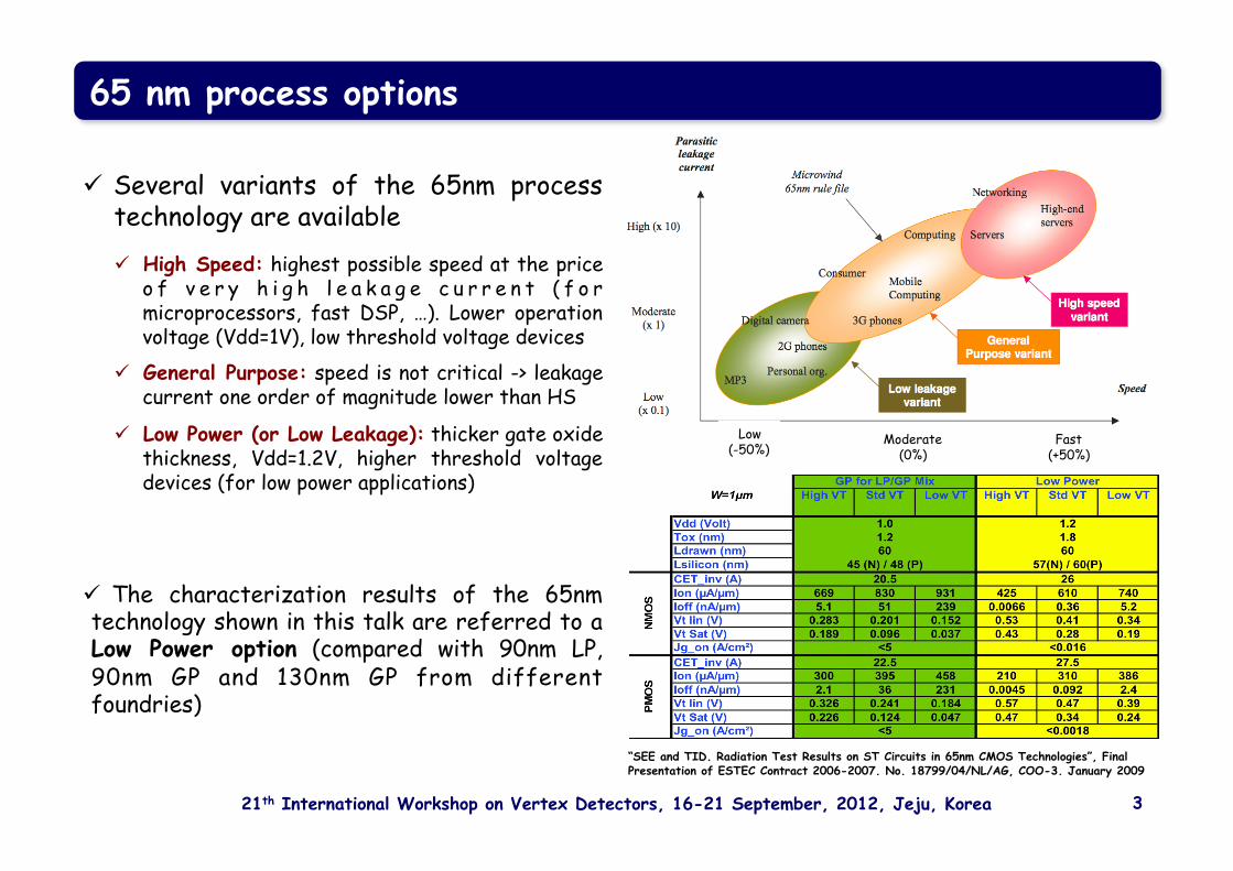
65 nm process options
3
Several variants of the 65nm process technology are available
High Speed: highest possible speed at the price o f v e r y h i g h l e a k a g e c u r r e n t ( f o r microprocessors, fast DSP, …). Lower operation voltage (Vdd=1V), low threshold voltage devices
General Purpose: speed is not critical -> leakage current one order of magnitude lower than HS
Low Power (or Low Leakage): thicker gate oxide thickness, Vdd=1.2V, higher threshold voltage devices (for low power applications)
The characterization results of the 65nm technology shown in this talk are referred to a Low Power option (compared with 90nm LP, 90nm GP and 130nm GP from different foundries)
Low (-50%)
Moderate (0%)
Fast (+50%)
“SEE and TID. Radiation Test Results on ST Circuits in 65nm CMOS Technologies”, Final Presentation of ESTEC Contract 2006-2007. No. 18799/04/NL/AG, COO-3. January 2009
21th International Workshop on Vertex Detectors, 16-21 September, 2012, Jeju, Korea
Outline
4
Analog performance of MOS transistors in 65nm technology Intrinsic gain Gate leakage current Noise performance Radiation hardness
Prototype chip with mixed-signal readout circuits in 65nm CMOS Features of the designed structures Experimental results
Collaborative activities under the AIDA WP3.3 Proposed IP blocks
21th International Workshop on Vertex Detectors, 16-21 September, 2012, Jeju, Korea
inversion level expressed by the inversion coefficient
where IZ* is the characteristic
normalized drain current
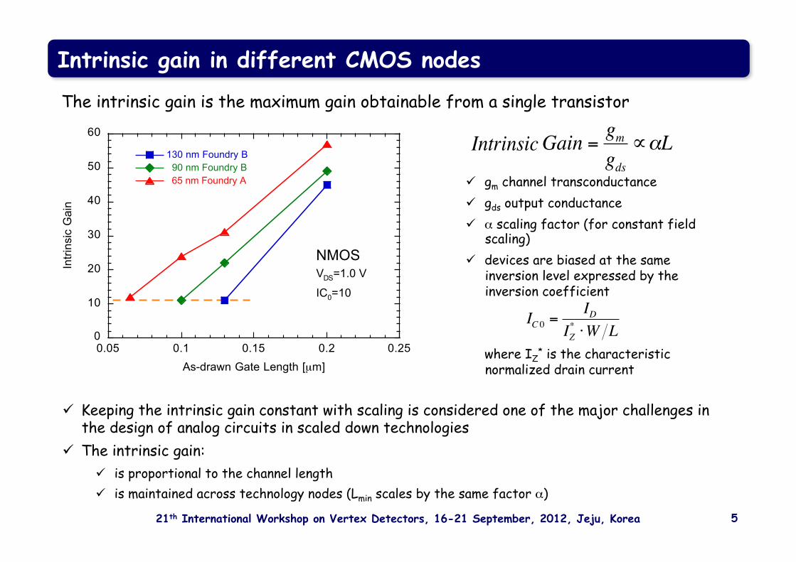
Intrinsic gain in different CMOS nodes
The intrinsic gain is the maximum gain obtainable from a single transistor
5
Keeping the intrinsic gain constant with scaling is considered one of the major challenges in the design of analog circuits in scaled down technologies
The intrinsic gain: is proportional to the channel length is maintained across technology nodes (Lmin scales by the same factor α)
0
10
20
30
40
50
60
0.05 0.1 0.15 0.2 0.25
130 nm Foundry B 90 nm Foundry B 65 nm Foundry A
Intri
nsic
Gai
n
As-drawn Gate Length [µm]
NMOSVDS=1.0 V
IC0=10
€
Gain =gmgds
∝αL
€
Intrinsic
€
IC 0 =ID
IZ* ⋅W L
21th International Workshop on Vertex Detectors, 16-21 September, 2012, Jeju, Korea
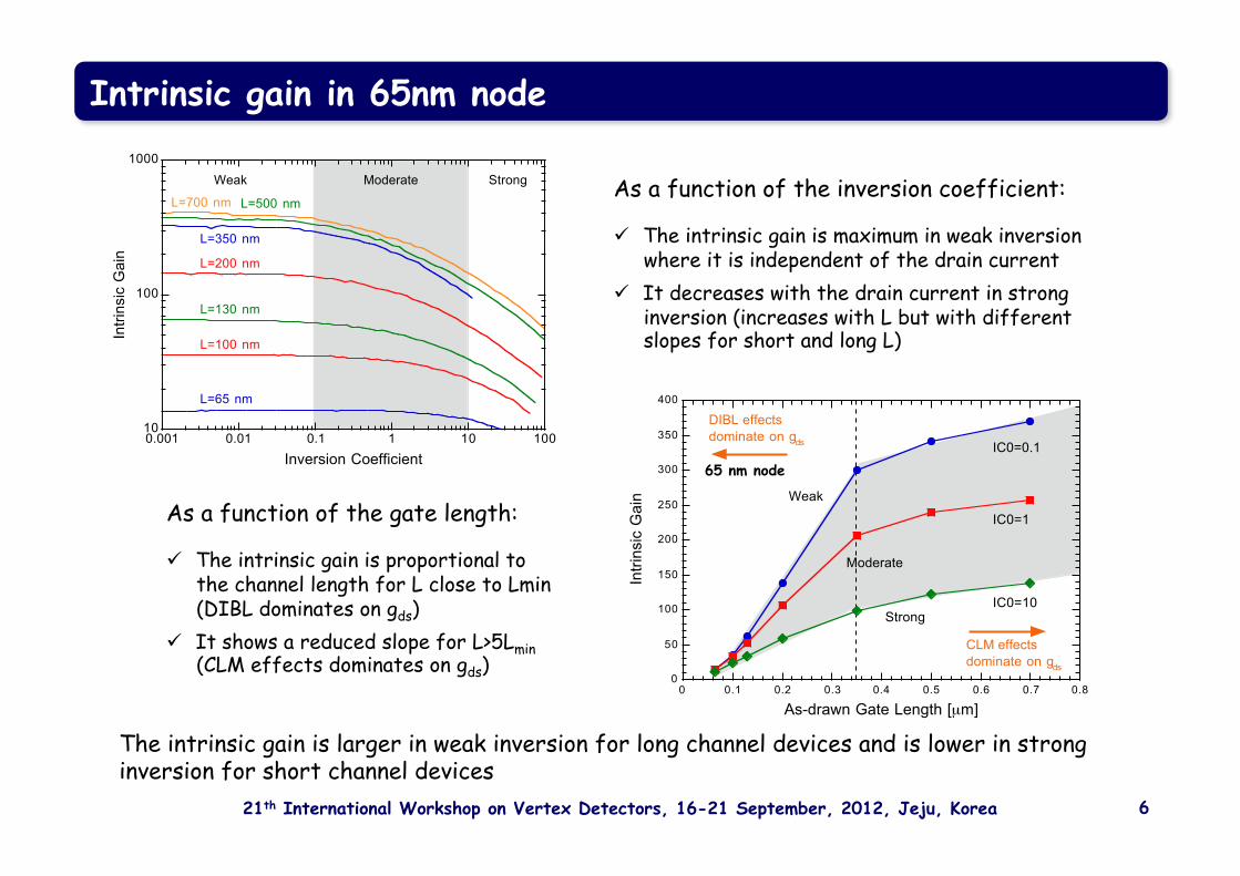
Intrinsic gain in 65nm node
6
10
100
1000
0.001 0.01 0.1 1 10 100
Intri
nsic
Gai
n
Inversion Coefficient
Weak Moderate Strong
L=65 nm
L=100 nm
L=130 nm
L=200 nm
L=350 nm
L=700 nm L=500 nm
0
50
100
150
200
250
300
350
400
0 0.1 0.2 0.3 0.4 0.5 0.6 0.7 0.8
Intri
nsic
Gai
n
As-drawn Gate Length [µm]
IC0=0.1
IC0=1
IC0=10
Weak
Moderate
Strong
DIBL effectsdominate on gds
CLM effectsdominate on gds
As a function of the inversion coefficient:
The intrinsic gain is maximum in weak inversion where it is independent of the drain current
It decreases with the drain current in strong inversion (increases with L but with different slopes for short and long L)
As a function of the gate length:
The intrinsic gain is proportional to the channel length for L close to Lmin (DIBL dominates on gds)
It shows a reduced slope for L>5Lmin (CLM effects dominates on gds)
The intrinsic gain is larger in weak inversion for long channel devices and is lower in strong inversion for short channel devices
65 nm node
21th International Workshop on Vertex Detectors, 16-21 September, 2012, Jeju, Korea
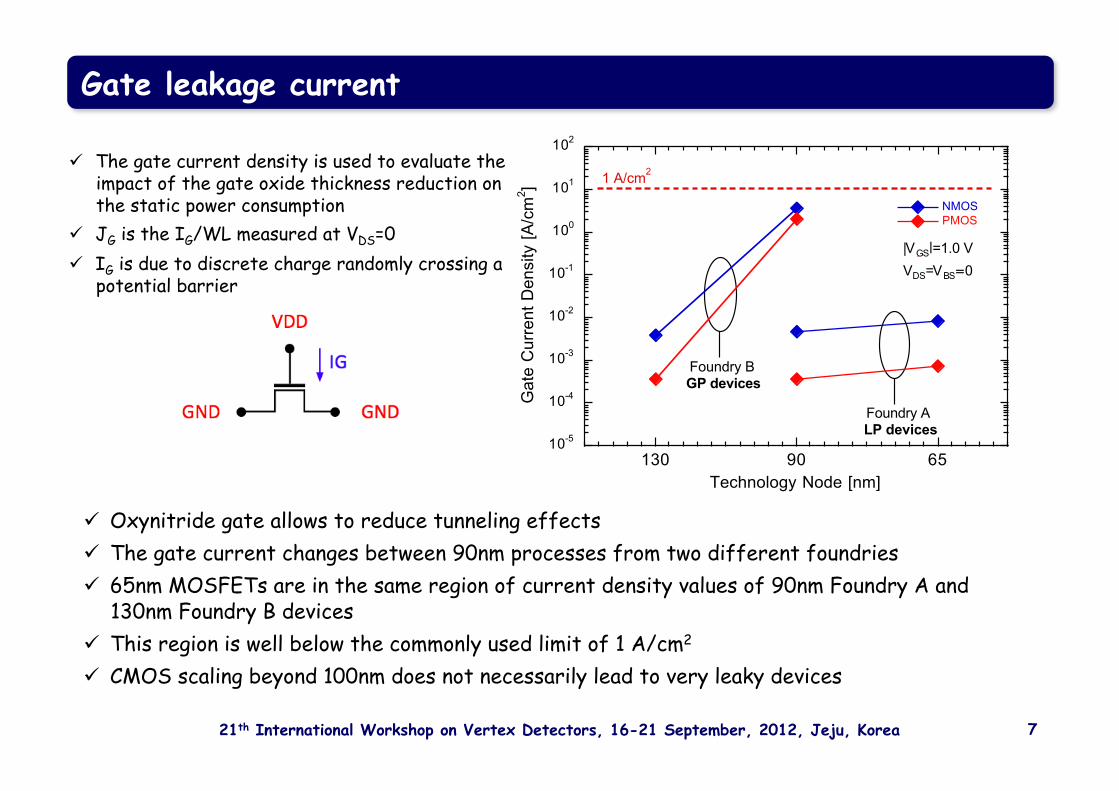
Gate leakage current
7
The gate current density is used to evaluate the impact of the gate oxide thickness reduction on the static power consumption
JG is the IG/WL measured at VDS=0 IG is due to discrete charge randomly crossing a
potential barrier
Oxynitride gate allows to reduce tunneling effects The gate current changes between 90nm processes from two different foundries 65nm MOSFETs are in the same region of current density values of 90nm Foundry A and
130nm Foundry B devices This region is well below the commonly used limit of 1 A/cm2 CMOS scaling beyond 100nm does not necessarily lead to very leaky devices
10-5
10-4
10-3
10-2
10-1
100
101
102
130 90 65
NMOS APMOS ANMOS BPMOS B
Gat
e C
urre
nt D
ensi
ty [A
/cm
2 ]
Technology Node [nm]
Foundry A LP devices
Foundry B GP devices
|VGS|=1.0 VVDS=VBS=0
1 A/cm2
21th International Workshop on Vertex Detectors, 16-21 September, 2012, Jeju, Korea
Noise in MOS transistors
8
S
DG
SW - white noise • channel thermal noise (main contribution in the
White and 1/f noise have been measured on test devices with different geometries and biased at different drain currents
Noise in the drain current of a MOSFET can be represented through an equivalent noise voltage source in series with the device gate
• kB Boltzmann’s constant
• T absolute temperature
• Γ channel thermal noise coefficient
• kf 1/f noise parameter
• αf 1/f noise slope-related coefficient
21th International Workshop on Vertex Detectors, 16-21 September, 2012, Jeju, Korea
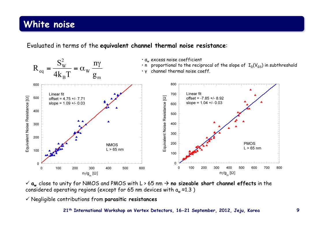
White noise
9
Evaluated in terms of the equivalent channel thermal noise resistance:
• αw excess noise coefficient • n proportional to the reciprocal of the slope of ID(VGS) in subthreshold • γ channel thermal noise coeff.
aw close to unity for NMOS and PMOS with L > 65 nm no sizeable short channel effects in the considered operating regions (except for 65 nm devices with aw ≈1.3 )
Negligible contributions from parasitic resistances
21th International Workshop on Vertex Detectors, 16-21 September, 2012, Jeju, Korea
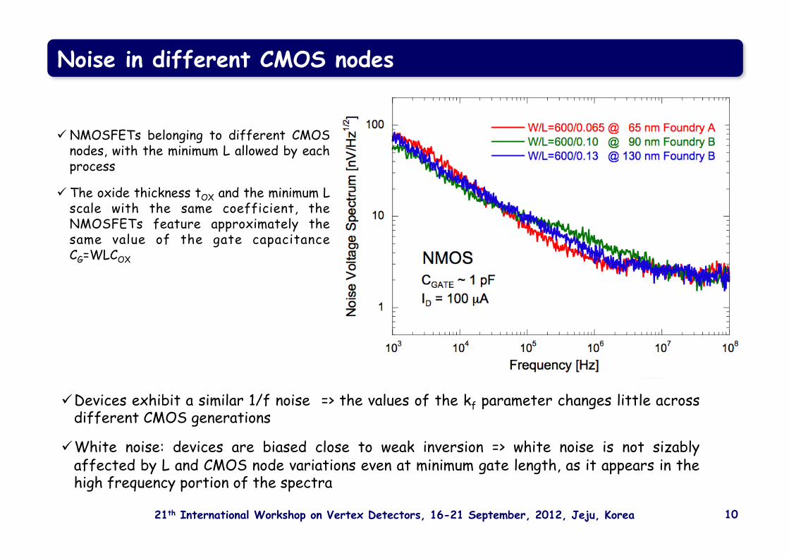
Noise in different CMOS nodes
10
NMOSFETs belonging to different CMOS nodes, with the minimum L allowed by each process
The oxide thickness tOX and the minimum L scale with the same coefficient, the NMOSFETs feature approximately the same value of the gate capacitance CG=WLCOX
Devices exhibit a similar 1/f noise => the values of the kf parameter changes little across different CMOS generations
White noise: devices are biased close to weak inversion => white noise is not sizably affected by L and CMOS node variations even at minimum gate length, as it appears in the high frequency portion of the spectra
21th International Workshop on Vertex Detectors, 16-21 September, 2012, Jeju, Korea
Ionizing radiation effects in sub-100 nm CMOS
11
The oxide thickness reduction and the substrate doping increase, due to the device scaling in CMOS technologies, improve the radiation hardness of deep submicron MOS transistors. The main degradation effects of devices exposed to ionizing radiation, are associated to the thick lateral isolation oxides (STI = Shallow Trench Isolation)
Radiation induced positive charge is removed from the gate oxide by tunneling (which also prevents the formation of interface states)
Isolation oxides remain thick (order of 100nm) also in nanoscale CMOS, and they are radiation soft
Radiation-induced positive charge trapped in isolation oxides may invert a P-type region in the well/substrate of NMOSFETs creating a leakage path between source and drain
In an interdigitated device this can be modeled considering that two lateral transistors for each finger are turned on
The effect of these parasitic devices on the noise and static characteristic must be carefully evaluated
21th International Workshop on Vertex Detectors, 16-21 September, 2012, Jeju, Korea
Ionizing radiation effects
12
10-10
10-8
10-6
10-4
10-2
100
-0.2 0 0.2 0.4 0.6 0.8 1
NMOS W/L = 1000/0.13V
DS=0.6V
total ID after irradiationID before irradiationID,lattotal ID after irradiationID before irradiationID,lat
Dra
in C
urre
nt[A
]
Gate-to-Source Voltage [V]
130 nm
65 nm
A large amount of lateral leakage takes places in 130nm devices
The smaller ID,lat of 65nm devices suggests that the sensitivity to positive charge buildup in STI oxides is mitigated by the higher doping of the P-type body with respect to less scaled technology
65 nm, before irradiation65 nm, 10 Mrad130 nm, before irradiation130 nm, 10 Mrad
Noi
se V
olta
ge S
pect
rum
[nV
/Hz1/
2 ]
Frequency [Hz]
Noise voltage spectra in the low frequency region are very similar before irradiation (similar gate capacitance)
1/f noise increase in the 130 nm device is significantly larger than in the 65 nm one
10 Mrad
21th International Workshop on Vertex Detectors, 16-21 September, 2012, Jeju, Korea
Noise in NMOSFETs
13
No increase in the white noise region is detected
At higher currents the degradation is barely detectable because the impact of the parasitic lateral devices on the overall drain current is negligible
PMOSFETs (not shown) do not feature any significant change in their static and noise properties after irradiation, following the trend of the most recent CMOS nodes
1
10
100
103 104 105 106 107 108
NMOS W/L=200/0.50@ Id=500 µA, Vds=0.6 V
before irradiation5 Mrad
Noi
se V
olta
ge S
pect
rum
[nV
/Hz1/
2 ]
Frequency [Hz]
1
10
100
103 104 105 106 107 108
NMOS W/L=200/0.50@ Id=50 µA, Vds=0.6 V
before irradiation5 Mrad
Noi
se V
olta
ge S
pect
rum
[nV
/Hz1/
2 ]
Frequency [Hz]
65 nm 65 nm
21th International Workshop on Vertex Detectors, 16-21 September, 2012, Jeju, Korea
Some remarks on the 65nm node
14
According to the study of key analog parameters, low-noise analog design in the 65nm CMOS node is viable
Intrinsic gain is not degraded by scaling
Gate leakage current is well below the limit of 1 A/cm2
Channel thermal noise behavior is consistent with equations valid in weak and moderate inversion
Flicker noise comparison with previous CMOS nodes shows that scaling to the 65nm process does not affect 1/f noise performance significantly
The comparison with data from previous generations confirms the high degree of radiation tolerance to ionizing radiation that appears to be typical of sub-100 nm technologies
Data analysis does not point out any novel damage mechanisms which could be related to the technological advances associated to an aggressively scaled process
We designed a prototype chip with mixed-signal readout circuits in the 65nm IBM CMOS process
21th International Workshop on Vertex Detectors, 16-21 September, 2012, Jeju, Korea
Apsel65: deep n-well monolithic active pixel sensor
15
Classical signal processing chain for capacitive detectors
The analog processor includes a charge sensitive amplifier, a shaping stage and a threshold discriminator binary readout
21th International Workshop on Vertex Detectors, 16-21 September, 2012, Jeju, Korea
Chip description
16
Chi Standalone channels Cinj = 30fF
Detector simulating cap. CD=250fF (CH1)
CD=350fF (CH2)
CD=450fF (CH3)
DNW sensor not connected
M1 3x3 matrix 40 µm pixel pitch
all analog outputs accessible Cinj = 30fF for central pixel
360 µm2 DNW electrode area
M2 8x8 matrix 40 µm pixel pitch
Row by row, 8-parallel digital readout
360 µm2 DNW electrode area
FCi FFE channels Cinj = 10fF
Detector simulating cap. CD=50fF (FC1)
CD=100fF (FC2)
CD=150fF (FC3)
21th International Workshop on Vertex Detectors, 16-21 September, 2012, Jeju, Korea
Apsel65: measurements
17
Measured ENC in good agreement with the simulated values
Charge collected by the central pixel as a function of the laser position Signal magnitude (normalized with respect to Vpk) is plotted in the z (colour) axis
for each position of the laser spot 5 µm step in X and Y (1064nm wavelength) The layout of the DNW and n-well layers has been superimposed (exact position
unknown) σxy of the laser ≈ 3 µm The main purpose of this measurement is to show the relative charge collection
versus position (the amount of charge that is deposited has not been calibrated)
Signal amplitude distribution for X-rays from an 55 Fe source (courtesy of S.Bettarini - INFN PI)
L. Gaioni, M. Manghisoni, L. Ratti, V. Re, G. Traversi, “A 65 nm CMOS prototype chip with monolithic pixel sensors and fast front-end electronics”, accepted for publication on IEEE Trans. on Nucl. Sci..
Recovery time increases linearly with the signal amplitude (C2 discharged by a constant current source) Charge sensitivity has an average value of 760 mV/fC (725 mV/fC simulated)
21th International Workshop on Vertex Detectors, 16-21 September, 2012, Jeju, Korea
Fast front-end for high resistivity pixels
18
W/L PA input device: 27/0.25 Power consumption: 6 µW ENC = 204 e- @ CD = 100 fF (measured: 214 e-) Simulated charge sensitivity: 42 mV/fC (measured: 37 mV/fC) Peaking time: ~ 25 ns (measured about 25 ns) Integral non linearity: ~ 3.5 % (32 ke- input dynamic range)
21th International Workshop on Vertex Detectors, 16-21 September, 2012, Jeju, Korea
AIDA (Advanced european Infrastructures for Detectors at Accelerators)
19
The AIDA project addresses infrastructures required for detector development for future particle physics experiments The infrastructures covered by the AIDA project are key facilities required for an efficient development of the future experiments, such as: test beam infrastructures (at CERN and DESY), specialised irradiation facilities (in several European countries), common software tools, common microelectronic tools and engineering coordination offices 4 year project More than 80 institutions and laboratories from 23 countries 3 main activities:
Networking WP2: Development of software common tools WP3: Microelectronics and detector/electronics integration
WP3.1: Coordination and communication WP3.2: 3D Interconnection WP3.3: Shareable IP blocks for HEP (65nm CMOS and SiGe)
WP4: Relations with industry Joint research
WP8: Improvement and equipment of irradiation and test beam lines WP9: Advanced infrastructure for detector R&D
Transnational access: supports small teams to carry out dedicated activities at one of the 5 European test facilities (DESY, CERN, JSI, KIT, UCL)
21th International Workshop on Vertex Detectors, 16-21 September, 2012, Jeju, Korea
AIDA WP3.3: collaborative activities on 65nm
20
WP3.3 task defines the plans for the creation of microelectronic libraries and IP blocks in advanced technologies to be made available to the community of users in HEP
The choice of the 65nm technology was prompted by the needs of future vertex detectors
The complexity of advanced microelectronic technologies demands for a critical mass of designers which shares knowledge and designs. This activity allows to exploit synergy in the HEP community
AIDA WP3.3 members set a common choice of technology option (65nm Low Power) and blocks of general interest to be developed
CERN is working to provide by Q2 2013 a new frame contract with a foundry
A common set of radiation characterization steps for the IP blocks has to be defined in order to have a uniform performance of the blocks in the applications
Some web-pages for documenting activities and results are being prepared allowing collaborative editing
21th International Workshop on Vertex Detectors, 16-21 September, 2012, Jeju, Korea
Proposed IP Blocks
21
Block Group Standard Cell Library CERN
CMOS IO Standard Library PADs CERN
LVDS IO PADs Bonn, INFN Pavia, AGH Krakow
SLVDS IO PADs Bonn, INFN Pavia, AGH Krakow
DAC LAL, CPPM, INFN Pavia
SRAM INFN Milano
Radiation Hardened Standard Cells INFN Milano, LAPP, CPPM, LPNHE
ADC Monitoring LAL, LAPP, CERN
Temperature Sensor CPPM, INFN Pavia
Bandgap References LAPP, CPPM, INFN Pavia
PLL AGH Krakow
ADC fast AGH Krakow
21th International Workshop on Vertex Detectors, 16-21 September, 2012, Jeju, Korea
Conclusion and future plans
Static, signal and noise measurements and radiation tests have been performed on devices belonging to a 65nm CMOS process
A test chip including deep N-well MAPS has been submitted in a 65nm CMOS process
Measurement results from this prototype circuit are encouraging and provide useful information for future submissions of larger chips
The 65nm CMOS technology is considered by designers a new attractive solution for the development of high performance front-end electronics in future applications
Shareable IP blocks for HEP
Organization of regular Microelectronics User Group meeting to exchange information, plan and coordinate actions related to the creation of a shared library of IP blocks
First submission of IP blocks in 65nm CMOS foreseen in 2013
22
21th International Workshop on Vertex Detectors, 16-21 September, 2012, Jeju, Korea
Backup slides
21th International Workshop on Vertex Detectors, 16-21 September, 2012, Jeju, Korea
Investigated technologies
21th International Workshop on Vertex Detectors, 16-21 September, 2012, Jeju, Korea
65nm CMOS devices
21th International Workshop on Vertex Detectors, 16-21 September, 2012, Jeju, Korea
Noise model for gate current in saturation
21th International Workshop on Vertex Detectors, 16-21 September, 2012, Jeju, Korea
Impact of gate current noise on resolution
21th International Workshop on Vertex Detectors, 16-21 September, 2012, Jeju, Korea
Device operation regions The actual inversion level of a MOSFET working in saturation can be expressed by means of its transconductance
efficiency which is defined as the ratio of the transconductance gm to the drain current Id
The slope of this parameter is zero in in the weak inversion (gm proportional to Id), while, in strong inversion the slope on a log scale is -1/2 (gm proportional to the square root of the drain current)
Moderate inversion is the transition region between weak and strong inversion. It is possible to define a characteristic normalized drain current Iz* located at the intersection of the wea k a n d a n d s t r o n g i n v e r s i o n asymptotes, which can be assumed to be the center of the moderate inversion region