Phase-Change Ge-Sb Nanowires: Synthesis, Memory Switching, and Phase-Instability Yeonwoong Jung, Chung-Ying Yang, Se-Ho Lee, and Ritesh Agarwal* Department of Materials Science and Engineering, UniVersity of PennsylVania, Philadelphia, PennsylVania 19104 Received February 25, 2009; Revised Manuscript Received March 25, 2009 ABSTRACT We report the synthesis and characterization of phase-change Ge-Sb nanowires with two different eutectic compositions and their memory switching characteristics. Under application of electric-fields with controlled pulse amplitude and duration times, Sb-rich (Sb g 86 at. %) eutectic Ge-Sb nanowires show phase-change based memory switching, while another eutectic GeSb (Ge:Sb ) 1:1) nanowires do not show electronic memory switching at all. However, under repeated measurements, Sb-rich Ge-Sb nanowires display an increase of resistance of the low resistive state. The observed electrical irreversibility for Sb-rich Ge-Sb nanowires is attributed to the structural and compositional instability due to the phase-separation of Ge out of homogeneous Ge-Sb as observed from rapid thermal annealing and transmission electron microscopy experiments. Implications for design of Te-free nanoscale materials for phase change memory applications are also discussed. Among a variety of materials developed to date for electronic phase-change memories (PCMs), Te-based ternary systems, such as Ge-Sb-Te alloys, have dominated the field. In PCMs, reversible structural change between crystalline and amorphous phases represents different electronic and optical states corresponding to changes in electrical resistivity and reflectivity, used for storing information. 1 Recently, Te-free Ge-Sb binary alloys emerged as a new class of phase-change materials. 2-8 In Ge-Sb systems, there are two eutectic compositions of Ge:Sb ) 1:1 and 0.14:0.86. 2 In particular, Sb-rich Ge-Sb alloys at/or above its eutectic limit (Sb g 86 at %) display many attributes of good phase-change materials for memory applications and offer several advan- tages over Ge-Sb-Te alloys. (1) The material is free of Te, which is an environmentally hazardous element and often chemically reacts with electrode metals in devices. 3 (2) It has a relatively high crystallization temperature of ∼250 °C leading to extremely long data retention times. 4 (3) Recrys- tallization mechanism is growth-dominated phase-change 5 as opposed to the nucleation-dominated behavior in Ge-Sb-Te, and the material possesses very fast crystallization speeds, 6-8 making it suitable for ultrafast data storages. 4-8 Despite such positive attributes, Ge-Sb alloys have been relatively unexplored in comparison to Ge-Sb-Te and the underlying phase-change mechanism remains poorly understood. In particular, the electronic properties of Sb-rich eutectic Ge-Sb and their feasibility for electronic memories have not been extensively investigated. Moreover, very few attempts have been made to synthesize Ge-Sb nanostructures, 9,10 which are expected to display superior properties due to their confined geometry at nanoscale. 11 In fact, recent studies of GeTe and Ge 2 Sb 2 Te 5 nanowires from our group have demonstrated advantages of using nanowires over thin-film devices, such as lower writing currents and power consump- tion due to current and heat localization, 12-14 size-dependent materials properties, 15 and enhanced functionalities by struc- tural/chemical modulation. 16 In this paper, we present a comprehensive study of Ge-Sb nanowire systems at different eutectic compositions to understand their phase change behavior at the nanoscale and to investigate their feasibility for phase-change based elec- tronic memory devices. We synthesized Ge-Sb nanowires with two different eutectic compositions, that is, Sb-rich Ge-Sb (Sb g 86 at. %) and GeSb (1:1), and characterized the structure and the composition of the nanowires by using X-ray diffraction (XRD), scanning/transmission electron microscopies (SEM/TEM), and energy-dispersive spectros- copy (EDS). We investigated the memory switching char- acteristics of two-terminal nanowires devices under sequen- tial application of AC voltage pulses and DC current-voltage (I-V) sweep and correlated their electrical properties with structural change using electron microscopy techniques. Ge-Sb nanowires were synthesized based on the vapor- liquid-solid mechanism 17 by thermal evaporation of Ge and Sb powders. Au colloid (∼100 nm)-deposited SiO 2 substrates were placed at the downstream side of a tube furnace. Ge * To whom correspondence should be addressed. E-mail: riteshag@ seas.upenn.edu. NANO LETTERS 2009 Vol. 9, No. 5 2103-2108 10.1021/nl900620n CCC: $40.75 2009 American Chemical Society Published on Web 04/24/2009
Department of Materials Science and Engineering, UniVersity of PennsylVania,Philadelphia, PennsylVania 19104
Received February 25, 2009; Revised Manuscript Received March 25, 2009
ABSTRACT
We report the synthesis and characterization of phase-change Ge-Sb nanowires with two different eutectic compositions and their memoryswitching characteristics. Under application of electric-fields with controlled pulse amplitude and duration times, Sb-rich (Sb g 86 at. %)eutectic Ge-Sb nanowires show phase-change based memory switching, while another eutectic GeSb (Ge:Sb ) 1:1) nanowires do not showelectronic memory switching at all. However, under repeated measurements, Sb-rich Ge-Sb nanowires display an increase of resistance ofthe low resistive state. The observed electrical irreversibility for Sb-rich Ge-Sb nanowires is attributed to the structural and compositionalinstability due to the phase-separation of Ge out of homogeneous Ge-Sb as observed from rapid thermal annealing and transmission electronmicroscopy experiments. Implications for design of Te-free nanoscale materials for phase change memory applications are also discussed.
Among a variety of materials developed to date for electronicphase-change memories (PCMs), Te-based ternary systems,such as Ge-Sb-Te alloys, have dominated the field. InPCMs, reversible structural change between crystalline andamorphous phases represents different electronic and opticalstates corresponding to changes in electrical resistivity andreflectivity, used for storing information.1 Recently, Te-freeGe-Sb binary alloys emerged as a new class of phase-changematerials.2-8 In Ge-Sb systems, there are two eutecticcompositions of Ge:Sb ) 1:1 and 0.14:0.86.2 In particular,Sb-rich Ge-Sb alloys at/or above its eutectic limit (Sb g86 at %) display many attributes of good phase-changematerials for memory applications and offer several advan-tages over Ge-Sb-Te alloys. (1) The material is free ofTe, which is an environmentally hazardous element and oftenchemically reacts with electrode metals in devices.3 (2) Ithas a relatively high crystallization temperature of ∼250 °Cleading to extremely long data retention times.4 (3) Recrys-tallization mechanism is growth-dominated phase-change5
asopposedtothenucleation-dominatedbehavior inGe-Sb-Te,and the material possesses very fast crystallization speeds,6-8
making it suitable for ultrafast data storages.4-8 Despite suchpositive attributes, Ge-Sb alloys have been relativelyunexplored in comparison to Ge-Sb-Te and the underlyingphase-change mechanism remains poorly understood. Inparticular, the electronic properties of Sb-rich eutectic Ge-Sband their feasibility for electronic memories have not been
extensively investigated. Moreover, very few attempts havebeen made to synthesize Ge-Sb nanostructures,9,10 whichare expected to display superior properties due to theirconfined geometry at nanoscale.11 In fact, recent studies ofGeTe and Ge2Sb2Te5 nanowires from our group havedemonstrated advantages of using nanowires over thin-filmdevices, such as lower writing currents and power consump-tion due to current and heat localization,12-14 size-dependentmaterials properties,15 and enhanced functionalities by struc-tural/chemical modulation.16
In this paper, we present a comprehensive study of Ge-Sbnanowire systems at different eutectic compositions tounderstand their phase change behavior at the nanoscale andto investigate their feasibility for phase-change based elec-tronic memory devices. We synthesized Ge-Sb nanowireswith two different eutectic compositions, that is, Sb-richGe-Sb (Sb g 86 at. %) and GeSb (1:1), and characterizedthe structure and the composition of the nanowires by usingX-ray diffraction (XRD), scanning/transmission electronmicroscopies (SEM/TEM), and energy-dispersive spectros-copy (EDS). We investigated the memory switching char-acteristics of two-terminal nanowires devices under sequen-tial application of AC voltage pulses and DC current-voltage(I-V) sweep and correlated their electrical properties withstructural change using electron microscopy techniques.
Ge-Sb nanowires were synthesized based on the vapor-liquid-solid mechanism17 by thermal evaporation of Ge andSb powders. Au colloid (∼100 nm)-deposited SiO2 substrateswere placed at the downstream side of a tube furnace. Ge
* To whom correspondence should be addressed. E-mail: [email protected].
NANOLETTERS
2009Vol. 9, No. 52103-2108
10.1021/nl900620n CCC: $40.75 2009 American Chemical SocietyPublished on Web 04/24/2009
and Sb powders were located inside the furnace with Ge inthe higher temperature region than Sb. The furnace temper-ature was ramped to 880 °C to simultaneously vaporize Geand Sb with a carrier Ar gas (200 SCCM) at a pressure of100 Torr. The temperature of the growth substrate was ∼400°C and the reaction was maintained for 1 h. The two differenteutectic compositions of Sb-rich Ge-Sb (Sb g 86 at %)and GeSb (1:1) were determined from the phase-diagram ofGe-Sb2 and were reliably achieved by controlling thelocation and the amount of Ge and Sb powders.
SEM image (Figure 1a) shows that as-grown nanowiresare typically 30-300 nm thick and >30 µm long when Geand Sb powders prepared in 0.14:0.86 molar ratio werethermally evaporated at 850 and 590 °C, respectively. TheXRD pattern of the as-grown nanowires (Figure 1b) matcheswith that of pure Sb in hexagonal structure [JCPDS 85-1324,space group: R3mj (no. 166)], consistent with previous studiesto report the solid-solution of Ge-Sb.18-20 With smallconcentration of Ge, it is known that Ge atoms occupyinterstitial sites of Sb lattice and do not distort the Sbstructure, therefore the crystalline phase is a solid solutionof Ge in Sb with the alloy structure remaining identical topure Sb.20 The chemical composition and the structure of
the nanowires were characterized with EDS in scanning TEM(STEM) and HRTEM. STEM elemental mapping images(Figure 1c) show the uniform distribution of Ge and Sbthroughout the nanowire with Au catalyst at the nanowiretip. EDS point scanning (Figure 1d) at arbitrary positionson the nanowire reveals that Ge and Sb are present in anatomic ratio of ∼0.12:0.88. EDS performed on a largenumber of nanowires confirmed that Sb is typically in a rangeof at % 0.86-0.90. HRTEM image (Figure 1e) of a Sb-richGe-Sb nanowire shows lattice fringes with spacing of 0.311nm corresponding to (012) crystal plane of hexagonal Sb (a) 4.3 Å, c ) 11.22 Å) consistent with the XRD analysis.The (012) orientation is also consistent with the previouslyreported growth direction of Sb nanobelts,21 as seen in thefast Fourier transform (FFT) of the HRTEM image (Figure1e, inset). Interestingly, in some nanowires stacking faultsare found along the nanowire growth direction. Figure 1f(left) is a TEM image of the side of a Sb-rich Ge-Sbnanowire showing that stacking faults proceed along thenanowire growth direction, while the HRTEM (right) clearlyreveals that alternating twin domains exist along [012]direction. These stacking faults were typically observed inthick nanowires (over ∼150 nm in diameter) that are foundin the hotter region of the furnace where the radial diameterof the nanowires increases due to the agglomeration ofmolten Au. Such structural variations are known to be dueto fast nanowire growth kinetics at high temperature,representing the competition between the diffusion rate insidethe catalyst droplet and the growth rate on the liquid-solidinterface.22,23 EDS study still confirms that Ge and Sb areuniformly distributed in as-grown nanowires in spite of thepresence of stacking faults (data not shown).
Ge-rich GeSb (1:1) nanowires were synthesized byevaporating Ge and Sb powders prepared in 1:1 molar ratioat 880 and 590 °C, respectively (Figure 2a, SEM image).High-resolution SEM reveals that the nanowires display well-faceted, rectangular cross sections, suggesting the single-crystallinity of the nanowires. XRD of the nanowires (Figure2b) matches well with the tetragonal GeSb pattern with Ge:Sb in 1:1 atomic ratio [ICDS 51652, space group: I4/mmm(no. 139)],2 and clearly differs from the XRD pattern of Sb-rich Ge-Sb nanowires (Figure 1b). The tetragonal structureof GeSb (1:1) nanowires is also consistent with the SEMobservation of rectangular cross sections. The chemicalcomposition of individual nanowires was found to be Ge:Sb ) ∼1:1 by EDS (Figure 2c), and STEM images showuniform spatial distribution of Ge and Sb in a large numberof nanowires (Figure 2d). The tetragonal GeSb structure wasfurther studied by HRTEM. HRTEM images reveal twolattice fringes (0.310 and 0.294 nm) intersecting at 90°,corresponding to (002) and (110) tetragonal planes respec-tively (Figure 2e, left inset). The indexed FFT (Figure 2e,right inset) obtained from the HRTEM image shows that thesingle-crystalline GeSb (1:1) nanowires grow along [001]direction. This TEM analysis combined with the XRDanalysis (Figure 2b) indicates that the frequently observedrectangular cross sections of GeSb (1:1) nanowires areattributed to the (001) tetragonal basal plane, and the
Figure 1. Sb-rich Ge-Sb (Sb g 86 at %) nanowires. (a) SEMimage of as-grown nanowires on SiO2 substrate. (b) XRD of Sb-rich Ge-Sb nanowires corresponding to hexagonal Sb structure.(c) STEM elemental mapping image to show uniform distributionof Ge and Sb with no phase-separation and Au at the nanowire tip.(d) EDS spectrum from the body of the same nanowire in panel c.(e) HRTEM of a Sb-rich Ge-Sb nanowire showing hexagonal (012)lattice fringes. Inset: FFT of the HRTEM confirms [012] growthdirection. (f) (left) TEM of a Sb-rich Ge-Sb nanowire to showstacking faults along the nanowire length; (right) HRTEM of theboxed region in the left to show that stacking faults proceeds in[012] direction.
2104 Nano Lett., Vol. 9, No. 5, 2009
nanowire side facet corresponds to the 110 crystal fam-ily.
The electrical memory switching properties of Ge-Sbnanowires were investigated by fabricating two-terminaldevices with Pt contacts (2 µm separation) deposited byfocused-ion-beam (FIB). DC I-V sweep of an as-synthesizedSb-rich Ge-Sb nanowire (∼80 nm thick) displays linear I-Vbehavior with an initial resistance of ∼36 kΩ (Figure 3a,red curve). Upon application of 200 ns voltage pulses withincreasing amplitude, the resistance is observed to suddenlyincrease at ∼6.2 V and saturates to ∼3.7 MΩ (Figure 3b).
The ratio of the resistance change reaches ∼100, whichsuggests crystalline-amorphous phase-change based memoryswitching.1,5,12-14 DC I-V sweep (Figure 3a, blue curve) ofthe amorphized nanowire device shows the initial highresistance is maintained until ∼4.0 V (threshold switching,Vth), after which the current increases and linear I-V behaviorreappears. Subsequent DC sweep (Figure 3a, black curve)displays linear behavior without threshold switching, indicat-ing the completion of amorphous-to-crystalline transition.However, the resistance is found to increase to ∼83 kΩ anddoes not fully recover its initial low value (∼36 kΩ) of theas-synthesized state prior to amorphization. This observationsuggests that the structure of the nanowires after voltagepulses/DC sweeps did not fully switch back to the initialstructure, which is in contrast to the completely reversibleswitching observed in GeTe and Ge2Sb2Te5 nanowires.12-14
Such lack of complete electrical reversibility was alsoobserved for other nanowires when phase-change wasintroduced by voltage pulses. Figure 3c shows the resistance(R) variation of another Sb-rich Ge-Sb nanowire (∼100 nmthick) under voltage pulses to realize crystalline-to-amor-phous (RESET) and amorphous-to-crystalline (SET) transi-tions. The initially crystalline nanowire (∼31 kΩ) reaches aRESET state (∼3.5 MΩ) with 200 ns voltage pulses above∼7.3 V (Figure 3c, red triangles) with a resistance ratio ofover ∼100. Subsequently, SET voltage pulses of longerduration (1 µs) were applied to the initially amorphizednanowire, and a low resistive crystalline state (∼92 kΩ) wasachieved above ∼5.1 V (Figure 3c, blue circles). It shouldbe noted that the resistance of the SET state (∼92 kΩ) isabout three times higher than the initial resistance (∼31 kΩ),resulting in the reduced resistance ratio of ∼40 betweenRESET/SET states. The irreversible change of the resistanceis further studied with another Sb-rich Ge-Sb nanowire(∼120 nm thick) under cyclic application of RESET/SETvoltage pulses. Under alternating RESET (8 V, 200 ns) andSET (6 V, 1 µs) voltages, the nanowire displays a cyclicresistance change between high/low resistive states (Figure3d). However, the SET resistance (Figure 3d, red squares)significantly increases (from ∼58 to ∼349 kΩ) as the deviceis repeatedly switched over 200 cycles, while the RESETresistance (Figure 3d, blue circles) remains relatively constantat ∼3.4 MΩ. We investigated a large number of nanowiresand consistently observed similar behavior; SET resistanceincreases and often saturates under repeated voltage pulses/DC-sweep leading to reduced RESET/SET resistance ratios,and the initial low resistance is never recovered. These datasuggest that phase-change in Sb-rich Ge-Sb nanowires isnot completely reversible in contrast to GeTe and Ge2Sb2Te5
nanowires.12-14 We also measured electrical switchingproperties of Ge-rich GeSb (1:1) nanowires by applyingvoltage pulses and failed to observe any memory switchingbehavior in all our devices; a majority of the as-synthesizednanowires do not show a noticeable change in the resistanceunder application of voltage pulses in our measurement range(up to 10 V), while some of thin nanowires (typically below∼80 nm) show a drastic resistance increase to over ∼1 GΩand saturate to this value, indicating electrical/structural
Figure 2. Ge-rich GeSb (1:1) nanowires. (a) SEM image of as-grown nanowires; (right) GeSb (1:1) nanowires with rectangularcross sections. (b) XRD of as-grown GeSb (1:1) nanowires. (c)EDS of GeSb (1:1) nanowires. (d) STEM mapping images of GeSb(1:1) nanowires. Scale bar: 300 nm. (e) TEM of a GeSb (1:1)nanowire. HRTEM (left inset) shows tetragonal (002) and (110)lattice fringes. FFT (right inset) confirms [001] growth direction.
Nano Lett., Vol. 9, No. 5, 2009 2105
breakdown of the device (Figure 3e). This high resistanceremains unchanged even under a cyclic application of voltagepulses with different amplitudes/durations as well as underDC I-V sweep, which confirms the failure of the device(Figure 3f). The absence of memory switching in GeSb (1:1) nanowires is possibly due to the higher melting temper-ature (∼670 °C) of 1:1 GeSb in comparison to Sb-richGe-Sb (∼590 °C),2 which will require very high voltage toamorphize the nanowires. Another possible reason to explainthe absence of the memory switching could be the uniqueelectronic properties of GeSb (1:1). Recently, Raoux et al.have reported that the resistivity of crystalline and amorphousphases of Ge-Sb thin-films with Ge 59.3% are very similar,therefore very little resistance change (<5 times) is expectedduring the phase-change.24 Meanwhile, the resistivity ratioin eutectic Sb-rich Ge-Sb thin-film (Ge ∼ 15 at %) reaches∼103, which suggests the drastic resistance change observedin our Sb-rich Ge-Sb nanowire indeed originates from thecrystalline/amorphous phase-change.24
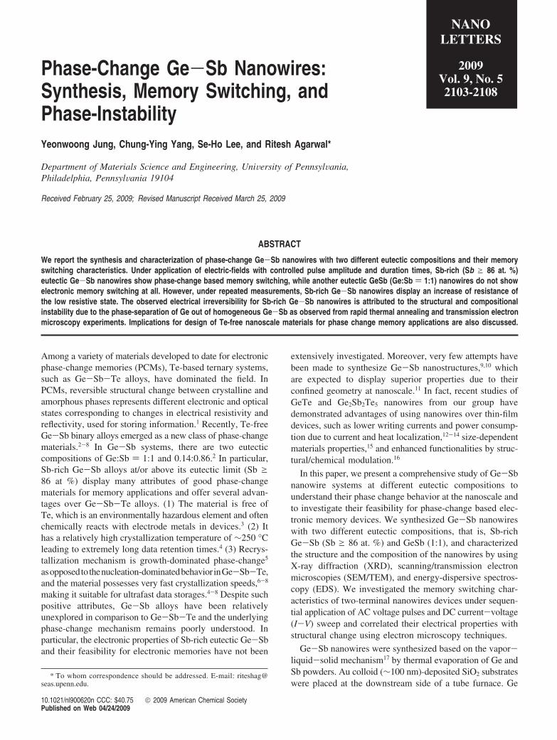
To understand the irreversible electrical switching of Sb-rich Ge-Sb nanowires, we examined the effect of heating/cooling on their structures by rapid thermal annealing (RTA)of freshly synthesized nanowires at 450 °C in Ar for 20 min(ramping rate: 30 °C/sec). TEM image (Figure 4a) of an
annealed Sb-rich Ge-Sb nanowire shows roughened surfacein comparison to preannealed nanowires, while HRTEMimage (Figure 4b) reveals polycrystalline structure showingcrystalline grains mixed with amorphous regions. EDS line-scan profile (superimposed in Figure 4a) across the samenanowire reveals uneven elemental distribution, showingbimodal distribution of Ge with higher concentration towardthe surface with localization of Sb at the core. The phase-separation becomes more pronounced when the annealingis performed at higher temperature (550 °C). STEM elemen-tal mapping image (Figure 4c) clearly shows Ge is pro-nouncedly segregated toward the surface while Sb is stilluniformly distributed. The data suggest that the nanowireundergoes phase-separation leading to Ge-rich surface throughannealing, and its structural/chemical homogeneity is notpreserved. Similar phenomena are also observed for GeSb(1:1) nanowires, while the degree of the phase-separation ismore pronounced than Sb-rich Ge-Sb nanowires. Interest-ingly, the phase-separation is observed in GeSb (1:1)nanowires after storing in air at room temperature for a longtime (>1 month). Figure 4d is a representative low-magnification TEM of GeSb (1:1) nanowires 12 months afterthe synthesis (stored at room temperature), displaying asimilar roughened surface as the annealed ones, which is in
Figure 3. Memory switching characteristics of Ge-Sb nanowire devices. (a) DC I-V sweep of a Sb-rich Ge-Sb nanowire (∼80 nm)device obtained from (1) as-synthesized state showing initial resistance of ∼36 kΩ, (2) after applying the amorphization voltage pulse (6.9V, 200 ns) showing clear threshold switching, and (3) after completing the DC sweep in (2) showing increased resistance to ∼83 kΩ. (b)Crystalline-to-amorphous phase-change of the same Sb-rich Ge-Sb nanowire in panel a. (c) RESET/SET transition of a Sb-rich Ge-Sbnanowire (∼100 nm) as a function of voltage pulses. (d) RESET/SET resistance variation of a Sb-rich Ge-Sb nanowire (∼120 nm) undercyclic voltage pulses (RESET, 8 V, 200 ns; SET, 6 V, 1 µs). (e) GeSb (1:1) nanowire (∼70 nm) shows electrical breakdown at ∼8 V underapplication of voltage pulses with increasing amplitude. (f) Constant high resistance of the same GeSb (1:1) nanowires under cyclic applicationof voltage pulses (red square, 9 V, 200 ns; blue triangle, 6 V, 1 µs) confirms permanent damage to the device.
2106 Nano Lett., Vol. 9, No. 5, 2009
clear contrast to the clean, single-crystalline surface of thefreshly synthesized nanowires (Figure 2a,e). RepresentativeHRTEM image (Figure 4e) clearly shows polycrystalline Gegrains segregated out of the Sb-rich host, suggesting thespontaneous phase-separation of Ge and Sb. These dataindicate the high tendency of phase-separation in Ge-Sbsystems, which become more pronounced with higherconcentration of Ge and also at higher temperatures.
In fact, recent studies of Ge-Sb thin-films (Ge:Sb ) 0.15:0.85) also report the precipitation of Ge upon high temper-ature (∼420 °C) annealing, which typically occurs at theinterface of thin film/metal contacts.25 We believe that ourGe-Sb nanowires also undergo phase-separation duringelectrical measurements, particularly in RESET transitionwhich requires Joule-heating above their melting tempera-tures (∼590 °C).2 The effect of phase-separation on theresistance can be qualitatively understood based on thestructural and compositional fluctuation. The resistance ofthe nanowires is determined by the effective cross-sectionalarea for carrier transport and the intrinsic resistivity whichvaries with the ratio of Ge/Sb. During the phase-separation,the nanowire core becomes Sb-rich, which is more electri-cally conductive25 than the surface which becomes Ge-rich.Meanwhile, the effective cross-sectional area of the Sb-rich
core becomes smaller with Ge localizing toward the surface,which contributes to increase the resistance of the crystallinephase. In addition, electron scattering from the polycrystallinegrain boundaries and defects can also contribute to theresistance increase. On the basis of the above analysis, thereason that GeSb (1:1) nanowires failed to show that thememory switching can also be attributed to their higherdegree of phase-separation along with higher density ofdefects, which will lead to carrier transport through two-separated Sb-rich and Ge-rich regimes, none of which areideal for phase-change memory applications. Also, as relativeSb concentration increases, the Sb-rich core will have lowercrystallization/melting temperatures than the homogeneous,eutectic Ge-Sb, since the transition temperatures of Sb islower than Ge (Tm ) ∼630 °C for Sb while Tm ) ∼920 °Cfor Ge).2 It is also known that Ge in contact with metalsgenerally crystallizes at much lower temperature than itsintrinsic crystallization temperature (60-70% of metal-Geeutectic temperatures), and the crystallization starts from themetal-Ge interface.25,26 This indicates that Ge-Sb phaseseparation in our nanowire devices may not be isotropic andmay initiate from the nanowire/Pt contacts. These factorsmake the precise interpretation of the resistance increase inGe-Sb nanowire devices difficult. Nevertheless, we believethe phase-separation at nanoscale causes the irreversibilityof memory switching, as observed in our electrical andannealing experiments.
We also compare the device performance of Sb-richGe-Sb nanowires with our previously reported GeTe andGe2Sb2Te5 nanowires. Sb-rich Ge-Sb nanowires displaysimilar RESET currents and power consumption in com-parison to Ge2Sb2Te5 nanowires of comparable thickness butare lower than those of GeTe nanowire. For example, thewriting current measured for ∼100 nm Sb-rich Ge-Sbnanowire is found to be 0.24 mA, corresponding to a powerof 1.6 mW, which is comparable to ∼1.5 mW reported forGe2Sb2Te5 nanowire, but lower than GeTe nanowire (∼2.0mW).27 The main reason for the observed lower writingcurrents could be the lower melting temperature of Sb-richGe-Sb (∼590 °C in bulk) in comparison to GeTe andGe2Sb2Te5 (Tm ) 725 °C for GeTe and 616 °C forGe2Sb2Te5).27 Other materials’ properties that affect thewriting currents/power consumption, such as thermal con-ductivity of Sb-rich Ge-Sb, are not well known in theliterature. The initial resistance ratio (∼102) of Sb-richGe-Sb nanowire is found to be similar to that of Ge2Sb2Te5
nanowire, while GeTe nanowires typically show largerresistance ratio (∼5 × 10²). Other device parameters suchas minimum device switching speed and maximum lifetimeunder cyclic test were not investigated in this study, mainlybecause of the complication in the measurements owing tothe electrical irreversibility.
This study presents a relatively unexplored but an impor-tant limitation of utilizing nanoscale Ge-Sb systems forPCMs despite their advantages in improved material proper-ties. Even though the precipitation of Ge appears as anapparent problem, pure Sb without introduction of foreignelements (such as Ge) is not a good choice for phase-change
Figure 4. TEM characterization showing the phase-separation inGe-Sb nanowires. (a) TEM image of a Sb-rich Ge-Sb nanowireafter annealing at 450 °C for 20 min with the corresponding EDSline-scan profiles superimposed. Bimodal distribution of Ge isobserved indicating phase-separation of Ge from Ge-Sb towardthe surface. (b) HRTEM of the same nanowire showing the phaseseparated region. (c) STEM elemental mapping image of a Sb-richGe-Sb nanowire after annealing at 550 °C revealing morepronounced Ge phase-separation. (d) TEM image of a GeSb (1:1)nanowire after being stored for 12 months in air at room temper-ature. (e) HRTEM image of the same nanowire shows polycrys-talline Ge grains segregated toward the surface of the GeSb (1:1)nanowire.
Nano Lett., Vol. 9, No. 5, 2009 2107
memory applications. The underlying role of Ge in theGe-Sb system is to enhance the structural stability, whichthereby realizes reliable memory switching. Pure amorphousSb has extremely fast crystallization speed; however, it easilyrelaxes back to the crystalline phase due to its low crystal-lization temperature (close to room temperature)28 causingdata volatility. An introduction of a small amount of asemiconductor with high melting temperature such as Geimproves the stability of amorphous phase as it increase thephase transition temperatures while preserving their fastcrystallization speeds.20 However, at this stage, the physicalorigin of Ge-Sb phase separation remains unknown, andpossible means to circumvent this problem needs furtherinvestigation. The present study also establishes the need forinvestigation of thermal stability of other recently developedSb-based phase-change materials such as doped Ge-Sb5 orSi-Sb29 at the nanoscale since the presence of a large surfacecan lead to rapid phase separation.
In summary, phase-change Ge-Sb nanowires with twodifferent eutectic compositions of Ge-rich GeSb (1:1) and Sb-rich Ge-Sb (Sb g 86 at %) were synthesized. No electric-field induced phase-change was observed in Ge-rich GeSbnanowires. Phase-change induced memory switching wasrealized in Sb-rich Ge-Sb nanowires however with partialirreversibility. TEM studies of Sb-rich Ge-Sb nanowires showphase-separation of Ge under thermal annealing, which isresponsible for the observed electrical irreversibility.
Acknowledgment. This work was supported by Grantsfrom NSF (DMR-0706381), Penn-MRSEC seed award(DMR05-20020), and in part by ONR (GrantN000140910116).
References(1) Hudgens, S.; Johnson, B. MRS Bull. 2004, 29, 829.(2) Giessen, B. C.; Borromee, C. J. Solid State Chem. 1972, 4, 447.(3) Krusin-Elbaum, L.; Cabral, C., Jr.; K. N. Chen, K. N.; Copel, M.;
Abraham, D. W.; Reuter, K. B.; Rossnagel, S. M.; Bruley, J.; Deline,V. R. Appl. Phys. Lett. 2007, 90, 1141902.
(4) Raoux, S.; Salinga, M.; Jordan-Sweet, J. L.; Kellock, A. J. Appl. Phys.2007, 101, 044909.
(5) Chen, Y. C.; et al. Tech. Dig. - Int. Electron DeVices Meet. 2006, 30,3.
(6) Van Pieterson, L.; van Schijndel, M.; Rijpers, J. C. N.; Kaiser, M.Appl. Phys. Let. 2003, 83, 1373.
(7) Afonso, C. N.; Solis, J.; Catalina, F.; Kalpouzos, C. Appl. Phys. Lett.1992, 60, 3123.
(8) Solis, J.; Afonso, C. N.; Trull, J. F.; Morilla, M. C. J. Appl. Phys.1994, 75, 7788.
(9) Sun, X.; Yu, B.; Ng, G.; Meyyappan, M.; Ju, S.; Janes, D. B. IEEETrans. Electron DeVices 2008, 55, 3131.
(10) Zhang, Y.; et al. Appl. Phys. Lett. 2007, 91, 013104.(11) Lieber, C. M.; Wang, Z. L. MRS Bulletin 2007, 32, 99.(12) Lee, S. H.; Ko, D. K.; Jung, Y.; Agarwal, R. Appl. Phys. Lett. 2006,
89, 223116.(13) Jung, Y.; Lee, S. H.; Ko, D. K.; Agarwal, R. J. Am. Chem. Soc. 2006,
128, 14026.(14) Lee, S. H.; Jung, Y.; Agarwal, R. Nat. Nanotechnol. 2007, 2, 626.(15) Lee, S. H.; Jung, Y.; Agarwal, R. Nano Lett. 2008, 8, 3303.(16) Jung, Y.; Lee, S. H.; Jennings, A. T.; Agarwal, R. Nano Lett. 2008,
8, 2056.(17) Wagner, R. S.; Ellis, W. C. Appl. Phys. Lett. 1964, 84, 89.(18) Yoo, Y.-G.; Yang, D.-S.; Ryu, H.-J.; Cheong, W.-S.; Baek, M.-C.
Mater. Sci. Eng., A 2007, 449, 627.(19) Afonso, C. N.; Morilla, M. C.; Solis, J.; Rizvi, N. H.; Ollacarizqueta,
M. A.; Catalina, F. Mater. Sci. Eng., A 1993, 173, 343.(20) Callan, J. P. Ultrafast Dynamics and Phase Changes in Solids Excited
by Femtosecond Laser Pulses. Ph.D Thesis, Harvard University,Cambridge, MA, 2002.
(21) Zhang, M.; Wang, Z.; Xi, G.; Ma, D.; Zhang, R.; Qian, Y. J. Cryst.Growth 2004, 268, 215.
(22) Lee, J. S.; Brittman, S.; Yu, D.; Park, H. J. Am. Chem. Soc. 2008,130, 6252.
(23) Hao, Y.; Meng, G.; Wang, Z. L.; Ye, C.; Zhang, L. Nano Lett. 2006,6, 1650.
(24) Raoux, S. et al. J. Appl. Phys. 2009, 105, 064918.(25) Cabral, C., Jr.; Krusin-Elbaum, L.; Bruley, J.; Raoux, S.; Deline, V.;
Madan, A.; Pinto, T. Appl. Phys. Lett. 2008, 93, 071906.(26) Tan, Z.; Heald, S. M.; Rapposch, M.; Bouldin, C. E.; Woicik, J. C.
Phys. ReV. B. 1992, 46, 9505.(27) Lee, S. H.; Jung, Y.; Chung, H.-S.; Jennings, A. T.; Agarwal, R.
Physica E 2008, 40, 2474.(28) Hashimoto, M.; Niizeki, T.; Kambe, K. J. J. Appl. Phys. 1980, 19,