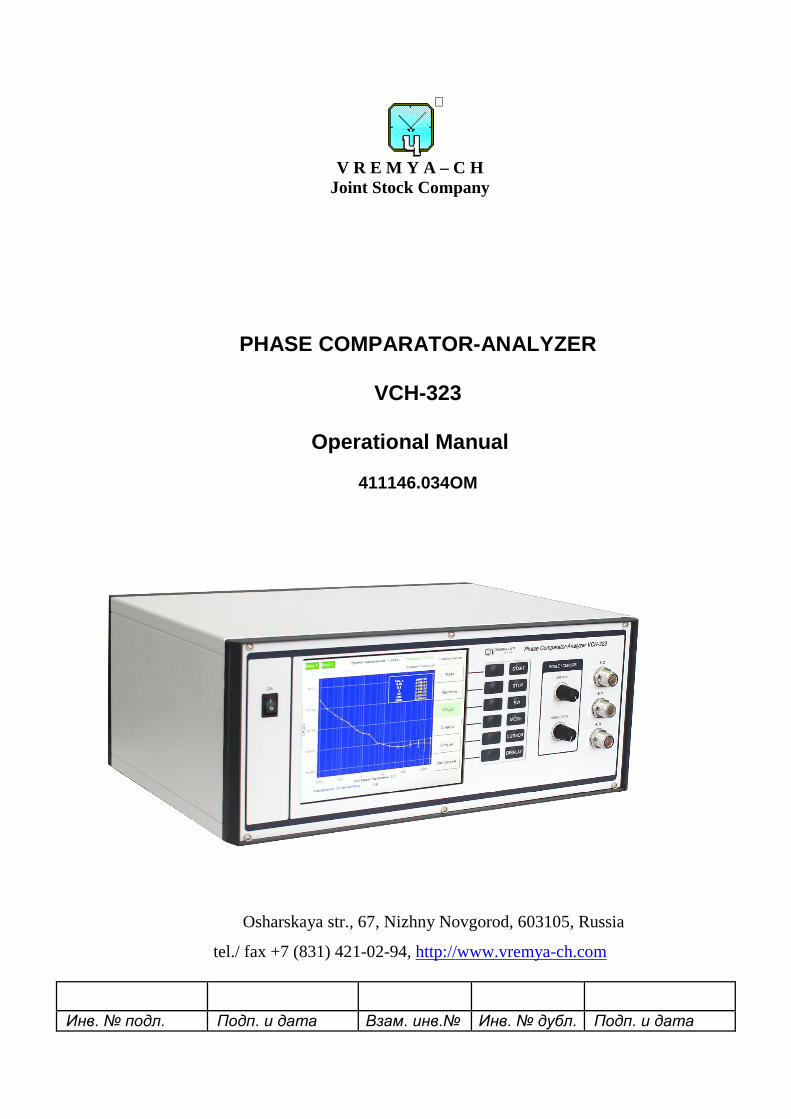
V R E M Y A – C H Joint Stock Company PHASE COMPARATOR-ANALYZER VCH-323 Operational Manual 411146.034OM Osharskaya str., 67, Nizhny Novgorod, 603105, Russia tel./ fax +7 (831) 421-02-94, http://www.vremya-ch.com Инв. № подл. Подп. и дата Взам. инв.№ Инв. № дубл. Подп. и дата
Transcript
V R E M Y A – C H
Joint Stock Company
PHASE COMPARATOR-ANALYZER
VCH-323
Operational Manual
411146.034OM
Osharskaya str., 67, Nizhny Novgorod, 603105, Russia
If input signals of the measuring channel have different frequencies it is
necessary to scale one of the phase differences with a coefficient equal to the
corresponding frequency ratio before subtraction.
In the obtained phase difference the noise of the clock generator is excluded, but
the noise added by the analog-to-digital conversion remains.
15
The circuit (Fig. 2) allows to significantly reduce the influence of ADC noise on
the results of measurements due to use of cross-correlation processing of phase
differences samples obtained in two parallel measuring channels. Measuring
channels use different ADC chips, so the noise they contribute can be
considered largely uncorrelated. In this case, cross-correlation processing allows
to reduce the level of noise introduced by analog-to-digital converters by
about 15 dB.
Phase difference samples are processed by the digital signal processor and the
built-in microcomputer (the DSP block in Fig. 2) that calculate the relative
frequency difference, ADEV, spectral density of the phase noise and perform
cross-correlation signal processing.
16
4 Preparing the device for use
4.1 Operational limitations
Operating conditions of the Device are given in p.3.2.
The Device should be kept under operating conditions for 24 hours after staying
in utmost conditions.
It is recommended to install the Device in a closed thermostated room.
ATTENTION! Do not place the Device near any engines, generators,
transformers, or other equipment that can produce magnetic fields and acoustic
vibrations. Placement near such equipment may impair the operation of the
Device.
The power supply of the Device is a voltage (220±22) V, (50±1) Hz AC.
The Device provides its specifications in working conditions after warm-up
time:
− 1 hour when measuring of phase noise spectral density and frequency
instability characteristics for averaging time range from 0.001 s to 100 s
inclusive;
− 4 hours when measuring of frequency instability characteristics for
averaging times more 100 s.
NOTE The input sinusoidal signals must be applied to the inputs of the Device
during the warm-up time.
WARNING! To turn off the Device, first switch the toggle on front panel to the
"O" position, wait at least 10 seconds, and only after that it is possible to
disconnect the Device from the AC mains.
17
4.2 Safety measures
4.2.1 Before usage you must ensure reliable grounding of the Device.
4.2.2 Ground terminal and conductors must be securely connected. To eliminate the
effect of static electricity, all subsequent connections must be made after the
Device is grounded.
4.3 Visual inspection
While inspecting the device make sure that:
− there are no visible mechanical defects;
− the seals are intact;
− the external surfaces of the Device, connectors, terminals and sockets are
clean;
− connecting cables and adaptors are in good condition;
− all ventilation holes in the Device cover are open, not blocked by other
objects.
4.4 Recommendations for using of peripheral devices
4.4.1 You can set the operating mode and control parameters of the Device using an
external monitor and a computer mouse.
4.4.2 Use a VGA monitor as an external monitor. The external monitor is connected to
the “VGA ” connector of the device using a VGA cable with DE15M connectors
(D-Sub 15, DB15HD).
4.4.3 The computer mouse is connected to the "USB2.0" or “PS/2” device connector.
WARNING! The device should be turned off before connecting the computer
mouse to the “PS/2” connector.
18
4.4.4 To copy the measurement results files to the user's computer using the FTP file
transfer protocol, you need to connect the device to the local network (Ethernet
network) by connecting the cable with the 8P8C connector to the LAN
connector of the Device.
An FTP client must be installed on the user's computer. Examples of such
programs are internet browsers or file managers.
19
5 Operating procedure
5.1 Location of control and connection systems
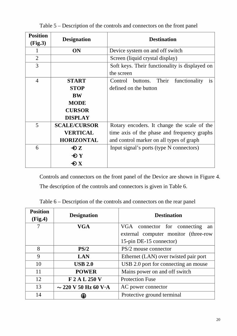
Controls and connectors on the front panel of the Device are shown in Figure 3.
The description of the controls and connectors is given in Table 5.
Figure 3. Controls and connectors on the front panel
Figure 4. Controls and connectors on the rear panel
20
Table 5 – Description of the controls and connectors on the front panel
Position (Fig.3)
Designation Destination
1 ON Device system on and off switch 2 Screen (liquid crystal display) 3 Soft keys. Their functionality is displayed on
the screen 4 START
STOP BW
MODE CURSOR DISPLAY
Control buttons. Their functionality is defined on the button
5 SCALE/CURSOR VERTICAL
HORIZONTAL
Rotary encoders. It change the scale of the time axis of the phase and frequency graphs and control marker on all types of graph
6 Z Y X
Input signal’s ports (type N connectors)
Controls and connectors on the front panel of the Device are shown in Figure 4.
The description of the controls and connectors is given in Table 6.
Table 6 – Description of the controls and connectors on the rear panel
Position (Fig.4)
Designation Destination
7 VGA VGA connector for connecting an external computer monitor (three-row 15-pin DE-15 connector)
8 PS/2 PS/2 mouse connector 9 LAN Ethernet (LAN) over twisted pair port 10 USB 2.0 USB 2.0 port for connecting an mouse 11 POWER Mains power on and off switch 12 F 2 A L 250 V Protection Fuse 13 220 V 50 Нz 60 V·A AC power connector
14 Protective ground terminal
21
5.2 Preparation for measurement
5.2.1 Carefully read the operating manual and make note of the location and purpose
of the controls on the front and rear panels of the Device.
5.2.2 Ensure the Device is properly grounded.
5.2.3 To reduce the measurement error it is recommended to minimize the effects of
acoustic and mechanical influences, electromagnetic emissions, drafts and
sudden changes in ambient temperature.
5.2.4 Connect (if necessary) the Device to Ethernet by connecting a cable with the
connector 8P8C to “LAN ” Device connector.
Connect (if necessary) the Device with an external monitor with a “VGA ”
device connector.
Connect (if necessary) the Device with a computer mouse, connecting it to the
“USB 2.0” or “PS/2” device connector.
5.2.5 Connect the Power connecting cord SCZ-1 with “ 220 V 50 Нz 60 V·A”
Device connector.
5.2.6 Turn on the power supply of the device from the AC mains by turning
“POWER” Device switch to position “I ” (on). Then turn the Device system on
by turning “ON” Device switch to position “I ” (on).
5.2.7 Connect the tested input signals according to the selected measurement mode
(see section 5.4).
NOTE The connection is made by coaxial cables with connectors of type N.
22
If coaxial cables with BNC connectors are connecting then adaptors N to BNC
33 N-BNC-50-1/133 UE should be used.
5.2.8 The Device will be ready for use with the guaranteed frequency instability noise
floor and phase noise floor after a one hour warm-up period.
5.2.9 To turn the Device off toggle "ON" switch to the "O" position, main program
will prepare the Device for shutdown and close, then the Device will turn off
automatically. The time between toggling the switch off and shutdown should
not less 10 seconds (and only after that it is possible to disconnect the Device
from the AC mains).
ATTENTION! The screen might glow without any text information while
turning on or off the Device. It is normal and does not indicate a malfunction!
23
5.3 Description of the user interface and measurement process
The Device is controlled by buttons and rotary encoders on the front panel, all
information about the progress and results of measurements is available on the
Device screen.
After switching on the operating system of the built-in computer and the main
control program will load and display information on the device status and
measurement results on the LCD screen.
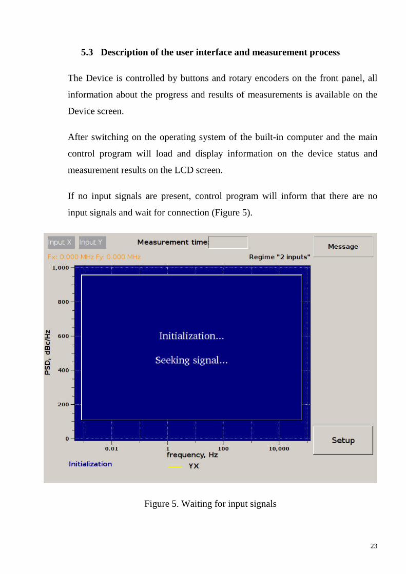
If no input signals are present, control program will inform that there are no
input signals and wait for connection (Figure 5).
Figure 5. Waiting for input signals
24
After at least two signals are connected to the input ports (connectors "X" and
"Y"), the control program will display information on the connected signals
(Figure 6) and begin preparing the Device for starting the measurements.
Figure 6. Preparing for measurements
When the preparation procedure is completed the main window of the control
program will look as shown in Fig. 7.
25
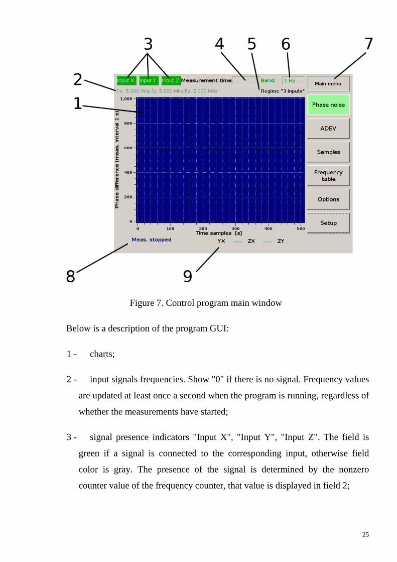
Figure 7. Control program main window
Below is a description of the program GUI:
1 - charts;
2 - input signals frequencies. Show "0" if there is no signal. Frequency values
are updated at least once a second when the program is running, regardless of
whether the measurements have started;
3 - signal presence indicators "Input X", "Input Y", "Input Z". The field is
green if a signal is connected to the corresponding input, otherwise field
color is gray. The presence of the signal is determined by the nonzero
counter value of the frequency counter, that value is displayed in field 2;
26
4 - time from the start of the measurement process (obtaining the first
sample);
5 - selected measurement mode;
6 - selected frequency band;
7 - selected menu and the buttons for this menu;
8 - state of the measurement process;
9 - chart color designation for the corresponding pair of signals.
Before measurements you must select one of two possible modes by pressing the
"MODE " button (group of control buttons pos.4 on Figure 3) and then the
corresponding mode keys (group of soft keys pos. 3 on Figure 3). Reference
signal for both channels of the comparator needs to be connected to the
" X" port for all measurement modes. Measurement modes are described
below.
1. "Two inputs" mode . See the soft keys group pos. 3 on Figure 3. This mode
allows you to reduce the noise introduced by the device when measuring the
characteristics of the frequency difference between the two signals using cross-
correlation processing. The signals must be connected to the " X" and " Y"
ports. In this mode, the signal connected to the " Y" is distributed to both
measuring channels (Figure 2). The frequency difference instability for the
analyzed signals is calculated by formula (6).
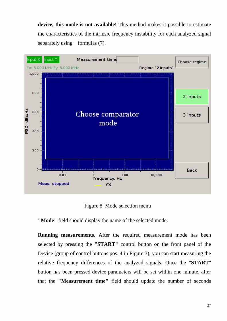
2. "Three Inputs" mode . See the soft keys group pos. 3 on Figure 3. In this
mode, the characteristics of the frequency instability are calculated using cross-
correlation processing by the “three-cornered hat” method. For this method three
different signals with similar frequency instability characteristics must be
connected to the Device inputs. If less than three signals are connected to the
27
device, this mode is not available! This method makes it possible to estimate
the characteristics of the intrinsic frequency instability for each analyzed signal
separately using formulas (7).
Figure 8. Mode selection menu
"Mode" field should display the name of the selected mode.
Running measurements. After the required measurement mode has been
selected by pressing the "START" control button on the front panel of the
Device (group of control buttons pos. 4 in Figure 3), you can start measuring the
relative frequency differences of the analyzed signals. Once the "START"
button has been pressed device parameters will be set within one minute, after
that the "Measurement time" field should update the number of seconds
28
elapsed since the first data was received, and in the lower left corner label
"Meas. stopped" should be replaced by "Meas. in progress".
Depending on the selected menu item the graphs field will show phase
differences (“Phase” item), relative frequency differences ("Frequency" item),
ADEV of the relative frequency difference, or ADEV of the frequency of each
signal separately in the "Three inputs" mode ("ADEV" item). The displayed
graphs have different colors, indicated at the bottom of the screen (Figure 6):
1) Yellow – for the difference characteristics of the signals at the inputs Y and X
or for the cross-correlation characteristics of the signal at the input X.
2) Blue – for the difference characteristics of the signals at the inputs Z and X or
for the cross-correlation characteristics of the signal at the input Y.
3) Green – for the difference characteristics of the signals at the inputs Z and Y
or for cross-correlation characteristics of the signal at the input Z.
Stopping measurements. To stop measurements, press the "STOP" control
button on the front panel of the Device.
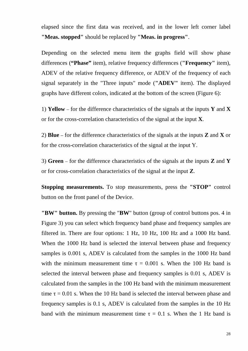
"BW " button. By pressing the "BW" button (group of control buttons pos. 4 in
Figure 3) you can select which frequency band phase and frequency samples are
filtered in. There are four options: 1 Hz, 10 Hz, 100 Hz and a 1000 Hz band.
When the 1000 Hz band is selected the interval between phase and frequency
samples is 0.001 s, ADEV is calculated from the samples in the 1000 Hz band
with the minimum measurement time τ = 0.001 s. When the 100 Hz band is
selected the interval between phase and frequency samples is 0.01 s, ADEV is
calculated from the samples in the 100 Hz band with the minimum measurement
time τ = 0.01 s. When the 10 Hz band is selected the interval between phase and
frequency samples is 0.1 s, ADEV is calculated from the samples in the 10 Hz
band with the minimum measurement time τ = 0.1 s. When the 1 Hz band is
29
selected the interval between phase and frequency samples is 1 s, ADEV is
calculated from the samples in the 1 Hz band with the minimum measurement
time τ = 1 s. The device performs measurements simultaneously in all four
bands, so you can change the band during measurements.
"DISPLAY" button. By pressing the "DISPLAY " button (group of control
buttons pos. 4 in Figure 3), you can choose which of the graphs or ADEV values
in the table should be displayed on the screen. You can enable or disable the
display of graphs during measurements.
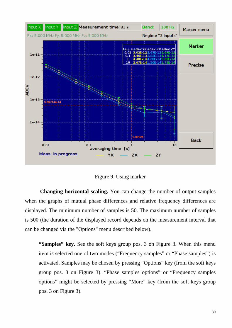
"CURSOR" button. When the "CURSOR" button (from the control buttons
group pos. 4 on Figure 3) is pressed screen will show the corresponding menu
(Figure 9), when the "Marker" key (from the soft keys group pos. 3 on Figure 3)
is active the graphs will show two crossing lines with vertical and horizontal
values. The position of the lines can be controlled by encoders on the front panel
of the Device (pos. 5 on Figure 3). When the "Precise" key is active, the
minimal marker movement step is reduced by a factor of 10.
If the " CURSOR " button (from the control buttons group pos. 4 on Figure 3) is
turned off the marker is not displayed and the "HORIZONTAL " encoder
(pos. 5 on Figure 3) controls the scale of mutual phase differences and relative
frequency differences graphs.
30
Figure 9. Using marker
Changing horizontal scaling. You can change the number of output samples
when the graphs of mutual phase differences and relative frequency differences are
displayed. The minimum number of samples is 50. The maximum number of samples
is 500 (the duration of the displayed record depends on the measurement interval that
can be changed via the "Options" menu described below).
“Samples” key. See the soft keys group pos. 3 on Figure 3. When this menu
item is selected one of two modes (“Frequency samples” or “Phase samples”) is
activated. Samples may be chosen by pressing “Options” key (from the soft keys
group pos. 3 on Figure 3). “Phase samples options” or “Frequency samples
options” might be selected by pressing “More” key (from the soft keys group
pos. 3 on Figure 3).
31
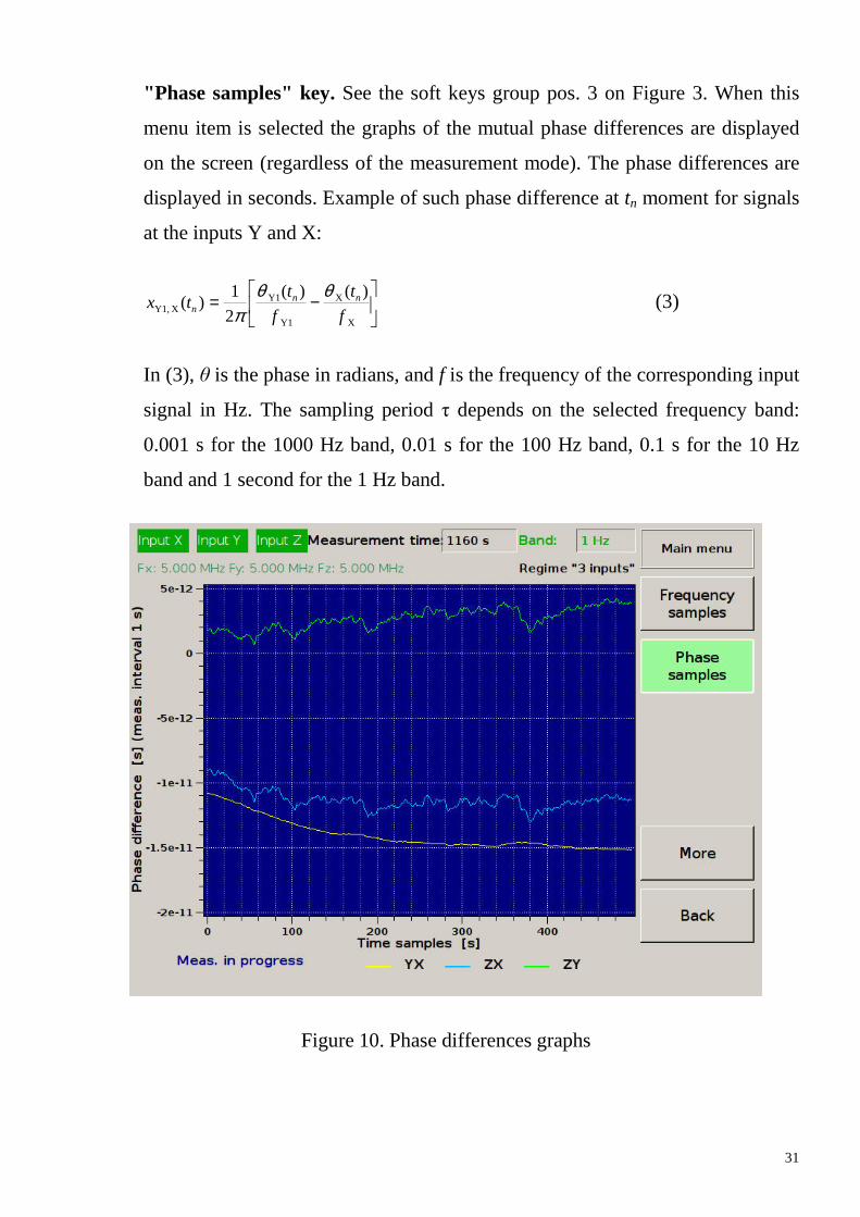
"Phase samples" key. See the soft keys group pos. 3 on Figure 3. When this
menu item is selected the graphs of the mutual phase differences are displayed
on the screen (regardless of the measurement mode). The phase differences are
displayed in seconds. Example of such phase difference at tn moment for signals
at the inputs Y and X:
−=
X
X
Y1
Y1 X Y1,
)()(
2
1)(
f
t
f
ttx nn
n
θθπ
(3)
In (3), θ is the phase in radians, and f is the frequency of the corresponding input
signal in Hz. The sampling period τ depends on the selected frequency band:
0.001 s for the 1000 Hz band, 0.01 s for the 100 Hz band, 0.1 s for the 10 Hz
band and 1 second for the 1 Hz band.
Figure 10. Phase differences graphs
32
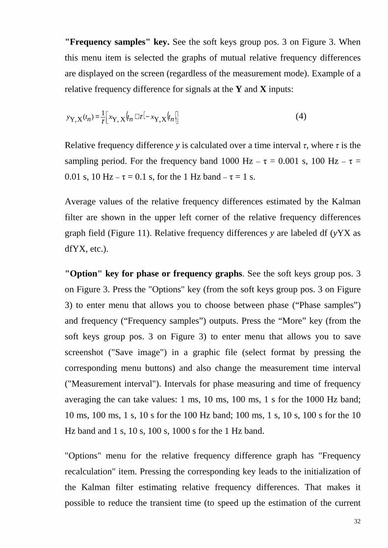
"Frequency samples" key. See the soft keys group pos. 3 on Figure 3. When
this menu item is selected the graphs of mutual relative frequency differences
are displayed on the screen (regardless of the measurement mode). Example of a
relative frequency difference for signals at the Y and X inputs:
( ) ( )
−+= ntxntxnty XY,X Y,
1)(XY, ττ (4)
Relative frequency difference y is calculated over a time interval τ, where τ is the
sampling period. For the frequency band 1000 Hz – τ = 0.001 s, 100 Hz – τ =
0.01 s, 10 Hz – τ = 0.1 s, for the 1 Hz band – τ = 1 s.
Average values of the relative frequency differences estimated by the Kalman
filter are shown in the upper left corner of the relative frequency differences
graph field (Figure 11). Relative frequency differences y are labeled df (yYX as
dfYX, etc.).
"Option" key for phase or frequency graphs. See the soft keys group pos. 3
on Figure 3. Press the "Options" key (from the soft keys group pos. 3 on Figure
3) to enter menu that allows you to choose between phase (“Phase samples”)
and frequency (“Frequency samples”) outputs. Press the “More” key (from the
soft keys group pos. 3 on Figure 3) to enter menu that allows you to save
screenshot ("Save image") in a graphic file (select format by pressing the
corresponding menu buttons) and also change the measurement time interval
("Measurement interval"). Intervals for phase measuring and time of frequency
averaging the can take values: 1 ms, 10 ms, 100 ms, 1 s for the 1000 Hz band;
10 ms, 100 ms, 1 s, 10 s for the 100 Hz band; 100 ms, 1 s, 10 s, 100 s for the 10
Hz band and 1 s, 10 s, 100 s, 1000 s for the 1 Hz band.
"Options" menu for the relative frequency difference graph has "Frequency
recalculation" item. Pressing the corresponding key leads to the initialization of
the Kalman filter estimating relative frequency differences. That makes it
possible to reduce the transient time (to speed up the estimation of the current
33
frequency difference) if the estimated frequency difference has significantly
changed its value during measurements.
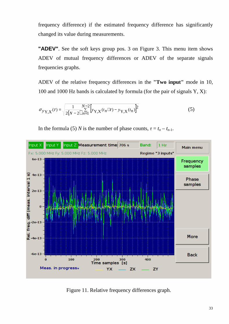
"ADEV". See the soft keys group pos. 3 on Figure 3. This menu item shows
ADEV of mutual frequency differences or ADEV of the separate signals
frequencies graphs.
ADEV of the relative frequency differences in the "Two input" mode in 10,
100 and 1000 Hz bands is calculated by formula (for the pair of signals Y, X):
( ) [ ]∑−
=−+
−=
2
1
2)(XY,)(XY,22
1)(XY,
N
nntynty
Ny ττσ (5)
In the formula (5) N is the number of phase counts, τ = tn – tn-1.
Figure 11. Relative frequency differences graph.
34
The ADEV of the relative frequency difference in 1 Hz band with measurement
time interval τ = mτ0 is calculated using the following formula with overlaps to
reduce the error associated with a finite number of counts:
( )( ) [ ]∑−
=++−+
−=
mN
nntxmntxmntx
mmNmy
2
1
2)(XY,)0(XY,2)02(XY,2
022
1)0(XY, ττ
ττσ (6)
In the formula (6) N is the number of phase counts, τ0 = tn – tn-1. = 1 s.
In the "Two inputs" measurement mode the noise added by the device (ADC
noise mainly) is reduced by cross-correlation processing. For the 100 Hz band,
the cross-correlation formula for calculating the ADEV is shown below:
( ) ∑−
=⋅
−=
2
1),(2 CHANNEL
XY,),(1 CHANNELXY,22
1)(XY,
N
nntnt
Ny τστστσ , (7)
where
)(CHANNEL1,2XY,)(CHANNEL1,2
XY,),(1,2 CHANNELXY, ntyntynt −+= ττσ (8)
– samples of the frequency variation in the corresponding measuring channel. In
the formula (7) N is the number of phase counts.
35
Figure 12. ADEV (σy)
For the 1 Hz band, the ADEV is calculated by the cross-correlation formula with
overlaps:
( )( ) ∑−
=⋅
−=
mN
nmntmnt
mmNmy
2
1)0,(2 CHANNEL
XY,~)0,(1 CHANNEL
XY,~
2022
1)0(XY, τστσ
ττσ
(9)
where
[ ])(XY,)0(XY,2)02(XY,0
1)0,(1,2 CHANNEL
XY,~ ntxmntxmntx
mmnt ++−+= ττ
ττσ (10)
36
– samples of the frequency variation in the corresponding measuring channel
calculated from the time-overlapping phase samples. In (9) N is the number of
phase counts.
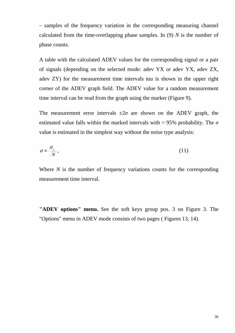
A table with the calculated ADEV values for the corresponding signal or a pair
of signals (depending on the selected mode: adev YX or adev YX, adev ZX,
adev ZY) for the measurement time intervals tau is shown in the upper right
corner of the ADEV graph field. The ADEV value for a random measurement
time interval can be read from the graph using the marker (Figure 9).
The measurement error intervals ±2σ are shown on the ADEV graph, the
estimated value falls within the marked intervals with ≈ 95% probability. The σ
value is estimated in the simplest way without the noise type analysis:
Nyσ
σ = , (11)
Where N is the number of frequency variations counts for the corresponding
measurement time interval.
"ADEV options" menu. See the soft keys group pos. 3 on Figure 3. The
"Options" menu in ADEV mode consists of two pages ( Figures 13, 14).
37
Figure 13. "Options" menu for ADEV, page 1
Using keys on the first page of the "ADEV options" menu (Figure 13) you can
save the current screen image in a graphic file (similar to phase and frequency
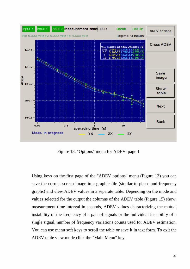
graphs) and view ADEV values in a separate table. Depending on the mode and
values selected for the output the columns of the ADEV table (Figure 15) show:
measurement time interval in seconds, ADEV values characterizing the mutual
instability of the frequency of a pair of signals or the individual instability of a
single signal, number of frequency variations counts used for ADEV estimation.
You can use menu soft keys to scroll the table or save it in text form. To exit the
ADEV table view mode click the "Main Menu" key.
38
Figure 14. "ADEV options" menu, page 2
39
Figure 15. ADEV table
To go to the second page of the "ADEV options" click the "Next" key
(Figure 13). The second page of the menu "ADEV options" is shown in
Figure 14. You can call up the table and intervals of the ADEV measurement
error on the ADEV graph using menu keys.
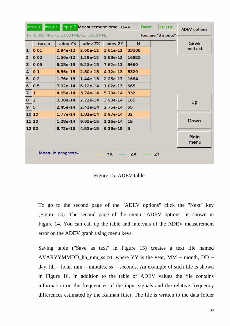
Saving table ("Save as text" in Figure 15) creates a text file named
AVARYYMMDD_hh_mm_ss.txt, where YY is the year, MM – month, DD –
day, hh – hour, mm – minutes, ss – seconds. An example of such file is shown
in Figure 16. In addition to the table of ADEV values the file contains
information on the frequencies of the input signals and the relative frequency
differences estimated by the Kalman filter. The file is written to the data folder
40
on the device (and to PC if remote control is active). It can be copied by
connecting to the device via FTP protocol (see below).
Figure 16. ADEV table file
"Phase noise" menu. See the soft keys group pos. 3 on Figure 3. "Phase noise"
menu shows the power spectral density (PSD) of the phase noise of the
measured signals. Power density is calculated by a weighted periodogram
method. The phase data x is divided into P non-overlapping segments with D
samples in each, so DP ≤ N, where N is the number of the samples. In each
segment the average phase difference for the given segment is subtracted from
sample then the values are weighed in Hann window:
][][][)( pDnxnwnx p += ,
−=D
nnw
π2cos15.0][
(12)
41
Then PSD is calculated for each segment using the FFT (D = 2k) and averaged:
( )∑ ∑−
=
−
=
−⋅⋅=1
0
21
0
2exp][11
25.2)(P
p
D
m
px fmTjmxT
DTPfS π
(13)
PSD for frequency f0 is calculated by the formula:
)(4)( 20
2 fSffS xπϕ = (14)
In "Two input" mode PSD is always calculated using the cross-correlation
method by multiplying spectral components from two channels. The result is
shown on the screen.
Figure 17. Spectrum for "Two input" mode
42
In "Three input" mode you can call up PSD graphs calculated by the cross-
correlation method for the phase noise of the XY and XZ channels and the
reference signal X.
Figure 18. Spectrum for "Three input" mode
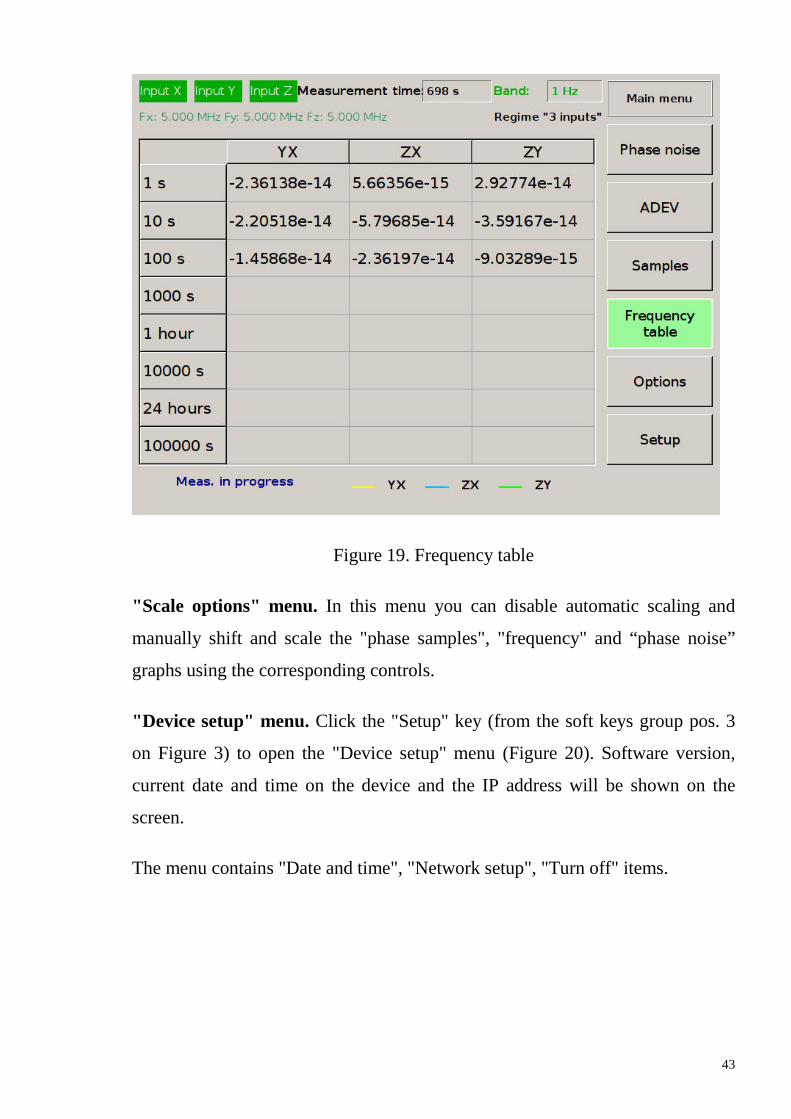
“Frequency table” menu. See the soft keys group pos. 3 on Figure 3.
Frequency table shows average relative frequency differences calculated for
different averaging times.
43
Figure 19. Frequency table
"Scale options" menu. In this menu you can disable automatic scaling and
manually shift and scale the "phase samples", "frequency" and “phase noise”
graphs using the corresponding controls.
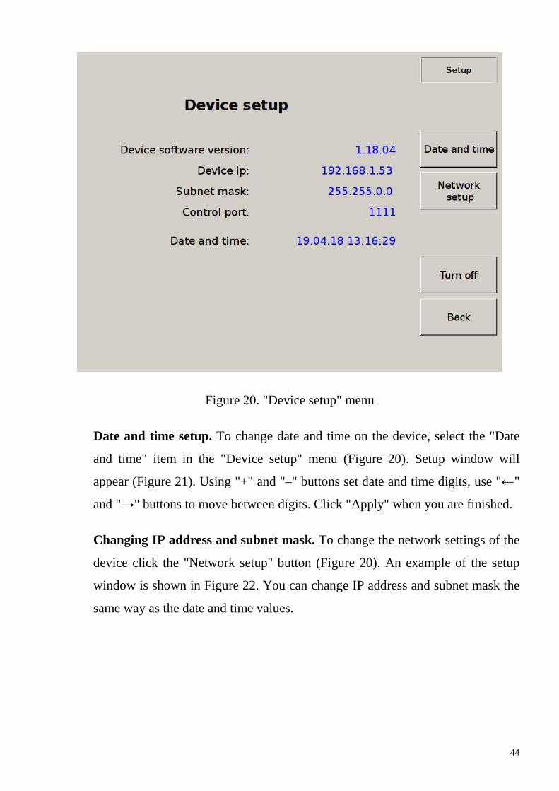
"Device setup" menu. Click the "Setup" key (from the soft keys group pos. 3
on Figure 3) to open the "Device setup" menu (Figure 20). Software version,
current date and time on the device and the IP address will be shown on the
screen.
The menu contains "Date and time", "Network setup", "Turn off" items.
44
Figure 20. "Device setup" menu
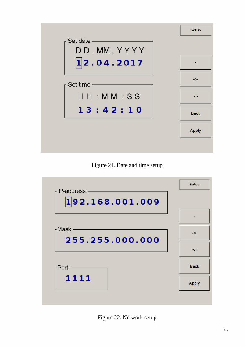
Date and time setup. To change date and time on the device, select the "Date
and time" item in the "Device setup" menu (Figure 20). Setup window will
appear (Figure 21). Using "+" and "–" buttons set date and time digits, use "←"
and "→" buttons to move between digits. Click "Apply" when you are finished.
Changing IP address and subnet mask. To change the network settings of the
device click the "Network setup" button (Figure 20). An example of the setup
window is shown in Figure 22. You can change IP address and subnet mask the
same way as the date and time values.
45
Figure 21. Date and time setup
Figure 22. Network setup
46
5.4 Copying data using FTP
The Device allows you to copy files using FTP protocol to a PC on the same
LAN with the device or directly connected to the device via LAN interface. FTP
server program starts automatically (with a LAN cable connected) after the
Device is turned on and the GUI is loaded. To copy files you need to establish
an FTP connection with the device using IP address shown in the device setup
menu (Figure 20). You can use the widespread Winscp client, FileZilla or
Internet browser. If there is no FTP connection, connect a LAN cable and reboot
the device.
Saved images files are located in the “image” directory. Files with the samples
of relative phase differences data are located in the “samples” directory.
Using FTP connection you can only copy to PC.
5.5 Measurement modes
5.5.1 "Two inputs" mode.
We can reduce the Device measurements error by using two identical measuring
channels (see Figure 2). In this case we supply the same signals Y and X to both
channels. Technically, this is done by switching the channel input from
connector “ Z” to connector “ Y” using a relay.
ADEV of the relative frequency differences in the "Two input" mode is
described by formula (for the pair of signals Y, X):
2 X
2 Y σσ +=adevYX , (15)
22, XY σσ – Allan variation of Y and X signals.
NOTE From a comparison of formula (15) and table 7 (number 1,2), it is seen
that the measurement error of ADEV for the pair of signals Y, X in "Two
47
inputs" mode is less than the measurement error for the pair of signals Y, X in
"Three inputs" mode due to the lack of instability introduced by the Device
measuring channels.
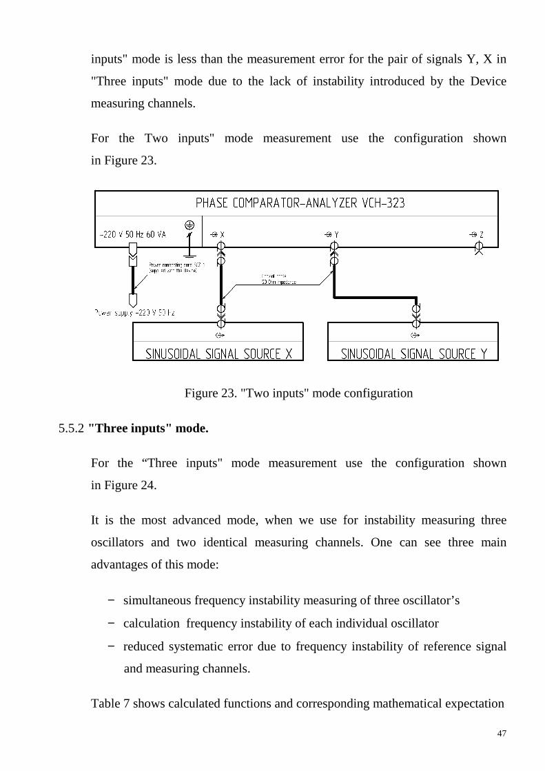
For the Two inputs" mode measurement use the configuration shown
in Figure 23.
Figure 23. "Two inputs" mode configuration
5.5.2 "Three inputs" mode.
For the “Three inputs" mode measurement use the configuration shown
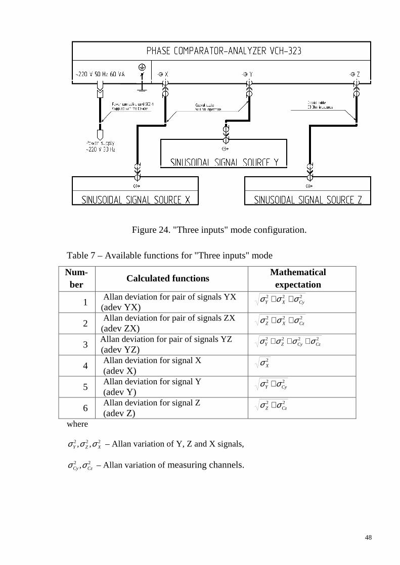
in Figure 24.
It is the most advanced mode, when we use for instability measuring three
oscillators and two identical measuring channels. One can see three main
advantages of this mode:
− simultaneous frequency instability measuring of three oscillator’s
− calculation frequency instability of each individual oscillator
− reduced systematic error due to frequency instability of reference signal
and measuring channels.
Table 7 shows calculated functions and corresponding mathematical expectation
48
Figure 24. "Three inputs" mode configuration.
Table 7 – Available functions for "Three inputs" mode
Num-ber
Calculated functions Mathematical expectation
1 Allan deviation for pair of signals YX (adev YX)
222CyXY σσσ ++
2 Allan deviation for pair of signals ZX (adev ZX)
222CzXZ σσσ ++
3 Allan deviation for pair of signals YZ (adev YZ)
2222CzCyZY σσσσ +++
4 Allan deviation for signal X (adev X)
2Xσ
5 Allan deviation for signal Y (adev Y)
22CyY σσ +
6 Allan deviation for signal Z (adev Z)
22CzZ σσ +
where
222 ,, XZY σσσ – Allan variation of Y, Z and X signals,
22 , CzCy σσ – Allan variation of measuring channels.
49
NOTE
Available functions number 1, 2, 3 are results, having systematic error due to
instability of reference signal X and measuring channels.
Available functions number 5, 6 are results, having systematic error due to
instability of measuring channels.
Available function number 4 is result having no systematic error.
Thus we can measure without systematic error only signal X.
NOTE All error calculations where made supposing that frequency fluctuations of
tested signals’ and comparators’ are independent. It is close to real practice only for
short-term stability (τ=1; 10 and may be 100 s).
50
6 Verification of the device
6.1 Introduction
This procedure is used to verify the basic measurement errors:
− frequency instability noise floor (the Allan deviation – ADEV) for
averaging times 0.01 s, 0.1 s, 1 s, 10 s, 100 s;
− phase noise floor L(f), (the Power spectral density – PSD),
for the input sinusoidal signal frequency 5 or 10 MHz (by user's choice) .
6.2 Service Equipment Required
Equipment required for the verification procedure is listed in Table 8.
Any equipment that satisfies the critical specification listed in the table 8 may be
substituted for the recommended models.
Table 8 – Equipment required for the verification procedure
Instrument (Quantity)
Required Characteristics Model
Sinusoidal signal sourse (1 piece)
- Outputs - number of ports: 2 - frequency: 5 MHz, 10 MHz - amplitude: (1.0±0.2) Vrms - load impedance: 50 Ohm - phase noise spectral density: not more –140 dBc/Hz - stability, two-samples Allan variance for averaging time 1 s: not more 5.0×10⁻¹¹
–––
Adaptor N to BNC (3 pieces)
Connectors: N plug , BNC jack. Impedance: 50 Ohm. Frequency range: 5 to 100 MHz
Adaptor N to BNC 33 N-BNC-50-1/133 UE
(supplied with the device)
51
Instrument (Quantity)
Required Characteristics Model
Two way reactive power divider (1 piece)
Connectors: SMA jack (4 pieces). Impedance: 50 Ohm. Frequency range: 5 to 10 MHz.
High Power Combiner
ZA3CS-400-3W-S (supplied with the device)
Special cables (3 pieces)
Coaxial cable, length: 0.2 to 0.5 meters Connectors: SMA cable plug, BNC cable plug. Impedance: 50 Ohm.
RF interconnecting SMA/BNC cable
685670.154 (supplied with the device)
Special cable (1 piece)
Coaxial cable, length: 1.0 to 3.0 meters Connectors: SMA cable plug , BNC cable plug. Impedance: 50 Ohm.
RF interconnecting SMA/BNC cable 685670.547 (supplied with the device)
6.3 Environmental Control
6.3.1 The quality of the measurements made by the Device is highly influenced by
environmental conditions.
6.3.2 The Device and all test equipment used during this verification procedure shall
be shielded from air drafts. Also, the device and all test equipment used during
this verification procedure shall be isolated from all sources of shock and


![A Fast Dynamic 64-bit Comparator with Small …downloads.hindawi.com/journals/vlsi/2002/535394.pdf · A Fast Dynamic 64-bit Comparator with Small Transistor ... phase logic [6] and](https://static.documents.pub/doc/80x56/5b7b4e627f8b9adb4c8c5a76/a-fast-dynamic-64-bit-comparator-with-small-a-fast-dynamic-64-bit-comparator.jpg)


