PhD Thesis Dissertation
Multifunctional Metamaterial Designsfor Antenna Applications
PhD Thesis Author
Pere Josep Ferrer GonzalezAntennaLab - TSC
Universitat Politecnica de Catalunya
E-mail: [email protected]
PhD Thesis Advisors
Jose Marıa Gonzalez Arbesu
and
Jordi Romeu Robert
AntennaLab - TSC
Universitat Politecnica de Catalunya
E-mail: [jmgonzalez, romeu]@tsc.upc.edu
Thesis submitted for the degree of Doctor of Phylosophy
from the Universitat Politecnica de Catalunya
Barcelona, June 2015
Multifunctional Metamaterial Designs for Antenna Applications
Pere Josep Ferrer Gonzalez
Ph.D. program on Signal Theory and Communications (TSC). Universitat Politecnica
de Catalunya (UPC). Barcelona (Spain)
This work has been partially supported by the Spanish Comision Interministerial de
Ciencia y Tecnologıa (CICYT) of the Ministerio de Educacion y Ciencia (MEyC)
and FEDER funds through the grants TEC2006-13248-C04-02/TCM, TEC2007-66698-
C04-01/TCM, TEC2007-65690, TEC2008-06764-C02-01, TEC2009-13897-C03-01/TEC,
and CONSOLIDER CSD2008-00068, by the Ramon y Cajal Programme and by the
European Commission through the METAMORPHOSE NoE project FP6/NMP3-CT-
2004-500252.
Copyright c©2015 by Pere Josep Ferrer Gonzalez, AntennaLab, TSC, UPC, Barcelona,
Spain. All rights reserved. Reproduction by any means or translation of any part of
this work is forbidden without permission of the copyright holder.
Abstract
Over the last decades, Metamaterials (MTMs) have caught the attention of the sci-
entific community. Metamaterials are basically artificially engineered materials which
can provide unusual electromagnetic properties not present in nature. Among other
novel and special EM applications, such as the negative refraction index (NRI) appli-
cation, Metamaterials allow the realisation of perfect magnetic conductors (PMCs),
which are of interest in the development of smaller and more compact antenna systems
composed of one or more antennas.
In this context, this thesis is focused on investigating the feasibility of using meta-
material structures to improve the performance of antennas operating at the microwave
frequencies. The metamaterial design process is challenging because metamaterials are
primarily composed of resonant particles, and hence, their response is frequency de-
pendent due to the dispersive behaviour of their effective medium properties. However,
one can take advantage of this situation by exploiting those strange properties while
finding other antenna applications for such metamaterial designs. For the case of the
PMC applications, the relative magnetic permeability values are negative, because they
are found just above the resonance of the metamaterial.
This thesis investigates several antenna applications of artificial magnetic materials
(AMMs). The initial work is devoted to the design of a spiral resonator (SR) AMM slab
to realise a low profile reflector dipole antenna by taking advantage of its PMC response.
The spiral resonator has been used due to its reduced unit cell size when compared to
other metamaterial resonators, leading to a more homogeneous metamaterial structure.
In addition, a bidirectional PMC spacer has been applied to produce a small and
compact antenna system composed of two monopole antennas, although the concept
may be applied to other antenna types. A third application as an AMC reflector are
the transpolarising surfaces, where the incident electric field plane wave is reflected at
a polarisation rotation angle of 90 degrees. Such surfaces may be of interest to produce
high cross-polar response reflecting devices, like the modified trihedral corner reflector
that has been tested for polarimetric synthetic aperture radar (PolSAR) purposes.
Another application of the SR AMM metamaterial is the patch antenna with a
magneto-dielectric loading. The relative magnetic permeability of the AMM meta-
i
material has values over the unity in the frequency band below the resonance. As a
consequence, the patch antenna can be miniaturised without reducing its bandwidth
of operation, in contrast to a typical high dielectric permittivity substrate.
Finally, the SR AMM metamaterial also presents values of relative magnetic perme-
ability between zero and the unity (MNZ). In such a case, the SR AMM metamaterial
has been applied as an MNZ cover of a slot antenna, devoted to increasing the broadside
radiated power and directivity of the antenna.
ii
Contents
1 Introduction 1
1.1 Motivation and thesis objectives . . . . . . . . . . . . . . . . . . . . . . 1
1.2 Thesis outline . . . . . . . . . . . . . . . . . . . . . . . . . . . . . . . . 2
2 Metamaterials in Antenna Engineering 5
2.1 Introduction to Metamaterials . . . . . . . . . . . . . . . . . . . . . . . 5
2.2 Metamaterials Applications . . . . . . . . . . . . . . . . . . . . . . . . 9
2.3 Metamaterials Applied to Antennas . . . . . . . . . . . . . . . . . . . . 10
2.3.1 Metamaterials in the Antenna Environment . . . . . . . . . . . 10
2.3.2 Metamaterials in the Antenna Structure . . . . . . . . . . . . . 16
2.3.3 Metamaterials in the Antenna Feeding Network . . . . . . . . . 18
2.4 Chapter Conclusions . . . . . . . . . . . . . . . . . . . . . . . . . . . . 20
3 Spiral Resonators as AMMs 21
3.1 Introduction . . . . . . . . . . . . . . . . . . . . . . . . . . . . . . . . . 21
3.2 AMM Characterisation . . . . . . . . . . . . . . . . . . . . . . . . . . . 22
3.2.1 Simplified modelling . . . . . . . . . . . . . . . . . . . . . . . . 22
3.2.2 MNG Measurement Setup . . . . . . . . . . . . . . . . . . . . . 26
3.3 Why Spiral Resonators as AMMs? . . . . . . . . . . . . . . . . . . . . . 30
3.4 Effective Medium Approach . . . . . . . . . . . . . . . . . . . . . . . . 36
3.5 Chapter Conclusions . . . . . . . . . . . . . . . . . . . . . . . . . . . . 42
4 AMMs as AMCs 43
4.1 Introduction . . . . . . . . . . . . . . . . . . . . . . . . . . . . . . . . 43
4.1.1 Single and double layer AMCs characterisation . . . . . . . . . 43
4.1.2 Fabrication of the prototypes . . . . . . . . . . . . . . . . . . . 48
4.1.3 S-parameter Measurement . . . . . . . . . . . . . . . . . . . . . 49
4.2 Single layer SR AMC as Antenna Reflector . . . . . . . . . . . . . . . . 52
4.2.1 Input Impedance . . . . . . . . . . . . . . . . . . . . . . . . . . 53
4.2.2 Radiation Patterns . . . . . . . . . . . . . . . . . . . . . . . . . 55
iii
4.3 Bidirectional AMCs for Compact Antenna Systems . . . . . . . . . . . 58
4.3.1 Spatial Diversity Antenna Systems . . . . . . . . . . . . . . . . 58
4.3.2 Two-Antenna System Design and Fabrication . . . . . . . . . . 59
4.3.3 Two-Antenna System Measurements . . . . . . . . . . . . . . . 61
4.3.3.1 S-parameters . . . . . . . . . . . . . . . . . . . . . . . 61
4.3.3.2 Envelope Correlation . . . . . . . . . . . . . . . . . . . 62
4.3.3.3 C-parameters . . . . . . . . . . . . . . . . . . . . . . . 63
4.3.3.4 Radiation Patterns . . . . . . . . . . . . . . . . . . . . 63
4.4 Chapter Conclusions . . . . . . . . . . . . . . . . . . . . . . . . . . . . 65
5 AMMs for Transpolarisation 67
5.1 Introduction . . . . . . . . . . . . . . . . . . . . . . . . . . . . . . . . . 67
5.1.1 Principle of Operation . . . . . . . . . . . . . . . . . . . . . . . 67
5.1.2 Potential Applications . . . . . . . . . . . . . . . . . . . . . . . 69
5.1.3 Transpolarising surface examples . . . . . . . . . . . . . . . . . 71
5.2 Transpolarisation with a SR AMM slab . . . . . . . . . . . . . . . . . . 72
5.2.1 Design and simulation of a transpolarising SR surface . . . . . . 72
5.2.2 Fabrication and measurement of a transpolarising SR surface . . 75
5.3 Design of a transpolarising surface . . . . . . . . . . . . . . . . . . . . . 77
5.4 Fabrication and Measurement . . . . . . . . . . . . . . . . . . . . . . . 81
5.4.1 Normal Incidence Measurements . . . . . . . . . . . . . . . . . . 81
5.4.2 Oblique Incidence Measurements . . . . . . . . . . . . . . . . . 85
5.5 Application to PolSAR Calibrator . . . . . . . . . . . . . . . . . . . . . 87
5.5.1 Introduction to Polarimetric Radar Calibration . . . . . . . . . 87
5.5.2 Transpolarising Surface Design . . . . . . . . . . . . . . . . . . 88
5.5.3 Field Measurement Results of the Transpolarising TCR . . . . . 89
5.5.3.1 Measurement Setup . . . . . . . . . . . . . . . . . . . 89
5.5.3.2 Measured Results . . . . . . . . . . . . . . . . . . . . . 91
5.6 Chapter Conclusions . . . . . . . . . . . . . . . . . . . . . . . . . . . . 95
6 Patch Antenna Miniaturisation with AMM Loadings 97
6.1 Introduction . . . . . . . . . . . . . . . . . . . . . . . . . . . . . . . . . 97
6.2 FBW computation techniques . . . . . . . . . . . . . . . . . . . . . . . 98
6.3 Homogeneous Substrate Patch Antenna Analysis . . . . . . . . . . . . . 102
6.3.1 Substrate parameters variation . . . . . . . . . . . . . . . . . . 104
6.3.1.1 Electric permittivity variation . . . . . . . . . . . . . . 104
6.3.1.2 Magnetic permeability variation . . . . . . . . . . . . . 106
6.3.1.3 Electric permittivity and magnetic permeability variation107
iv
6.3.2 Losses in the Patch Antenna Substrate . . . . . . . . . . . . . . 108
6.3.3 Discussion on Bandwidth and Patch Antenna Miniaturisation . 110
6.4 Patch Antennas with Dispersive Metamaterial Loadings . . . . . . . . . 113
6.4.1 SR AMM Design as a Metasubstrate . . . . . . . . . . . . . . . 114
6.4.2 Simulation of Patch Antennas with AMM Metasubstrates . . . . 116
6.4.3 Fabrication of Patch Antennas with AMM Metasubstrates . . . 124
6.4.4 Measurement of Patch Antennas with AMM Metasubstrates . . 125
6.4.4.1 Radiation Efficiency . . . . . . . . . . . . . . . . . . . 128
6.4.4.2 Radiation Patterns . . . . . . . . . . . . . . . . . . . . 129
6.5 Chapter Conclusions . . . . . . . . . . . . . . . . . . . . . . . . . . . . 130
7 Leaky Wave Antennas with AMM Mu-Near-Zero Slabs 133
7.1 Introduction . . . . . . . . . . . . . . . . . . . . . . . . . . . . . . . . . 133
7.2 MNZ slabs for broadside radiation improvement . . . . . . . . . . . . . 135
7.3 Slot Antenna Design for MNZ Applications . . . . . . . . . . . . . . . . 137
7.4 Fabrication of the MNZ Slot Antenna System . . . . . . . . . . . . . . 138
7.5 Measurements of the MNZ Antenna . . . . . . . . . . . . . . . . . . . . 139
7.5.1 Return Loss . . . . . . . . . . . . . . . . . . . . . . . . . . . . . 139
7.5.2 Radiation Patterns . . . . . . . . . . . . . . . . . . . . . . . . . 140
7.6 Chapter Conclusions . . . . . . . . . . . . . . . . . . . . . . . . . . . . 146
8 Conclusions 147
8.1 Main conclusions . . . . . . . . . . . . . . . . . . . . . . . . . . . . . . 147
8.2 Future research lines . . . . . . . . . . . . . . . . . . . . . . . . . . . . 149
A Time-Domain Gating Method 151
B List of Publications 159
C List of Acronyms 163
Bibliography 167
v
Chapter 1
Introduction
1.1 Motivation and thesis objectives
Since the end of the twentieth-century, the development of mobile communication
systems has grown together with the increasing demand for Internet and localisation
services (VoIP, messaging, browsing, streaming, GPS). Year by year, the electronics
systems design industry has become increasingly focused on realising smaller mobile
transmitting/receiving (Tx/Rx) devices, while maintaining or increasing data capacity
and signal coverage. Consequently, miniaturised antennas are in increasing demand. In
addition, multiple antenna systems (MIMO), which traditionally suffer from couplings
between the antenna elements, are often used to improve the signal quality and coverage
in complex propagation scenarios such as urban or indoor environments. Therefore,
the antenna design strategies have become more complex.
On the other hand, over the last decades, Metamaterials (MTMs) have caught the
attention of the scientific community [1–16]. Metamaterials are basically artificially
engineered materials which can provide unusual electromagnetic properties not present
in nature. The first theoretical study was carried out by the Russian physicist V.G.
Veselago in 1968 [17], introducing the possibility of left-handed media (LHM). In the
late-90’s, the British physicist J.B. Pendry investigated the feasibility of fabricating
those metamaterials proposed 30 years before [18] from the combination of different
1
2 1.2. Thesis outline
types of electric conductors. Finally, the American physicist D.R. Smith and co-workers
demonstrated experimentally the LHM behaviour [19, 20]. In the mid 2000’s, the
project Metamorphose NoE, funded by the European Commission through the FP6
programme, led to the creation of a European scientific community network among
electrical engineers and physicists working with Metamaterials.
In terms of Electromagnetics (EM), metamaterial properties can be applied from
Microwave frequencies (MHz-GHz) to Optics (THz), continuously leading to new dis-
coveries and applications, such as later metamaterial applications found in Acous-
tics [21, 22]. Among other novel and special EM applications, such as the negative
refraction index (NRI) application [19], Metamaterials allow the realisation of perfect
magnetic conductors (PMCs) [8], which are of interest in the development of smaller
and more compact antenna systems composed of one or more antennas. The antenna
system can be miniaturised when using metamaterials, because they are able to over-
come and reduce the λ/4 distance requirement of a linear antenna placed above (or
opposite) a perfect electric conductor (PEC), that is, a reflecting metallic surface.
PMCs are theoretically predicted in the Image Current Theory [23], but very little at-
tention has been reported by the scientific community to the proper realisation of such
structures at microwave frequencies (MHz-GHz). One drawback of metamaterials is
that the resulting PMC condition in the designed metamaterials may only be achieved
within a narrow frequency bandwidth of operation.
In this context, the thesis is focused on investigating the feasibility of different meta-
material designs devoted to improve the performance of antennas operating at the GHz
frequencies, like the artificial PMCs (AMCs) for compact and low profile antenna ap-
plications. The metamaterial design process is challenging because metamaterials are
primarily composed of resonant particles, and hence, their response is frequency de-
pendent due to the dispersive behaviour of their effective medium properties. However,
one can take advantage of this situation by exploiting those strange properties while
finding other antenna applications for such metamaterial designs.
1.2 Thesis outline
This thesis is organised as follows. Chapter 2 introduces the basics of metamateri-
als, as well as a compilation of metamaterials applied to antennas. Chapter 3 presents
the properties study of spiral and loop-like magnetic metamaterial inclusions, where
the spiral resonator (SR) is chosen as the artificial magnetic material (AMM) to be
used as artificial PMC, as well as, in other antenna applications that will be discussed
in the following chapters. Chapter 4 focuses on the low profile dipole reflector de-
sign and a compact two-antenna system using the SR AMMs. Chapter 5 introduces a
Chapter 1. Introduction 3
polarisation conversion property of a metamaterial reflector, which is also applied to
polarimetric synthetic aperture radar (PolSAR) calibration with a modified trihedral
corner reflector (TCR). Chapter 6 studies the bandwidth and patch antenna miniatur-
isation possibilities when using magneto-dielectric (MD) metamaterial and SR AMM
substrates. Chapter 7 presents a broadside power and directivity increase study when
using a SR AMM cover of a slot antenna. Finally, Chapter 8 concludes this thesis and
gives some suggestions for further research lines in AMM metamaterials for antenna
applications.
Chapter 2
Metamaterials in
Antenna Engineering
2.1 Introduction to Metamaterials
Metamaterials (MTMs) were first introduced by Veselago [17], who considered that
the constitutive values ε (electric permittivity) and µ (magnetic permeability) of an
effectively homogeneous material could take simultaneously negative values. As a con-
sequence of that, several physical phenomena could change their natural behaviour,
such as the reversal of Snell’s law, the reversal of Doppler shift, the reversal of Cerenkov
effect, among others. The constitutive material parameters ε and µ, are related to the
refractive index n as:
n = ±√εrµr (2.1)
where εr and µr are the relative permittivity and permeability related to the free space
permittivity ε0 = ε/εr ≈ 8.85 · 10−12 F/m and permeability µ0 = µ/µr = 4π · 10−7
H/m.
Then, four possible regions appear depending on the sign combinations of (ε, µ);
since ε0 and µ0 are positive fundamental constants, negative values in ε = ε0εr and
5
6 2.1. Introduction to Metamaterials
µ = µ0µr are due to the sign of the relative parameters εr and µr, respectively. An
ε−µ diagram has been depicted in Figure 2.1 representing the possible materials arising
from the four sign combinations of (ε, µ).
Figure 2.1: ε− µ diagram. In this graph, ε = ε0εr and µ = µ0µr.
Waves can only propagate in materials from regions I and III, where ε and µ pa-
rameters are both positive (double positive, DPS, or right-handed medium, RHM) or
both negative (double-negative, DNG, or left-handed medium, LHM). Non propagat-
ing evanescent waves are found in regions II and IV, where ε < 0 (epsilon negative,
ENG) or µ < 0 (mu negative, MNG). Finally, some other regions of interest might
also be considered, such as the epsilon-near-zero (ENZ) where 0 < |ε| < 1, and the
mu-near-zero (MNZ) where 0 < |µ| < 1.
Double negative metamaterials (DNG) are characterised by their simultaneous ε < 0
and µ < 0 values. This fact also affects the field equations in Maxwell’s formulas. A
general definition of the Poynting vector ~S in a phasor notation is (2.2), where a time
dependence e+jωt and a space dependence e−jkr are assumed:
~S =1
2~E × ~H∗ (2.2)
where the electric field ~E and the magnetic field ~H are defined by:
~β × ~E = ωµ ~H
~β × ~H = −ωε~E
(2.3)
Chapter 2. Metamaterials in Antenna Engineering 7
Therefore, for an isotropic and homogeneous medium with ε > 0 and µ > 0, the
electric field ~E, the magnetic field ~H and the propagation vector ~β form a right-handed
triplet, which is the origin of the right-handed medium (RHM) definition. However, by
considering a medium with ε < 0 and µ < 0, the previous equations can be rewritten
as:
~β × ~E = −ω |µ| ~H
~β × ~H = ω |ε| ~E(2.4)
showing that the ~E − ~H − ~β forms a left-handed triplet. This medium is referred to
as left-handed medium (LHM), and supports backward waves, because the Poynting
vector ~S is opposite the propagation vector ~β, that is, the energy and wavefronts travel
in opposite directions. This fact is reflected in the RHM and LHM ~E − ~H − ~β triplets
depicted in Figure 2.2.
Figure 2.2: ~E − ~H − ~β triplets for right-handed and left-handed media.
The DNG behaviour was first achieved by combining two single negative materials,
this is, a wire/rodded medium (introduced in 1962 by W. Rotman [24] as artificial
dielectrics) which provides the required ε < 0, and a split ring resonator (SRR) medium
(introduced in 1999 by J.B. Pendry [18]) which provides the required µ < 0. The SRRs
were initially realized as cylindrical conducting structures with longitudinal gaps [18],
although first metamaterial prototypes were fabricated from the combination of planar
SRRs, etched on a thin dielectric layer, and metallic rods [19]. In addition, a two-
dimensional metamaterial design was also presented taking advantage of the two sides
of the dielectric layers, this is, by etching the SRRs on one side of the dielectric layer,
and the planar strips (equivalent to the wires) on the opposite one [20]. Some of the
first fabricated metamaterial samples are shown in Figure 2.3.
However, the wire medium and the SRRs medium are frequency dependent due to
their strong resonant behaviour (Drude-Lorentz models), and hence, DNG metamateri-
als are also frequency dependent. For this reason, the refraction index n is reformulated
as:
n ≡ neff (ω) =√
εeff (ω)µeff (ω) (2.5)
8 2.1. Introduction to Metamaterials
(a) 1D design (b) 2D design
Figure 2.3: First fabricated metamaterial designs composed of SRRs and rods/strips[19, 20].
where εeff (ω) and µeff (ω) are the frequency dependent effective permittivity and the ef-
fective permeability, respectively. These effective material parameters are characterised
by their Drude-Lorentz dispersion models, and have the form described in (2.6).
εeff (ω) = 1−ω2ep − ω2
e0
ω2 − ω2e0 + jωνc
µeff (ω) = 1− Fω2
ω2 − ω2m0 + jωΓ
(2.6)
where ωep and ωmp are the electric and magnetic plasma frequencies, ωe0 and ωm0 are
the electric and magnetic resonant frequencies, νc is the collision frequency, F is an
amplitude factor and Γ is a damping factor. These expressions have been plotted in
Figure 2.4.
−9
−8
−7
−6
−5
−4
−3
−2
−1
0
1
Frequency
ε eff
Real(εeff )Imag(εeff )
ωep
(a) Effective permittivity
−8
−6
−4
−2
0
2
4
6
Frequency
µeff
Real(µeff )Imag(µeff )
ωm0 ωmp
(b) Effective permeability
Figure 2.4: Effective material functions for a DNG metamaterial.
The negative parameter frequency bands are located above the resonant frequency
Chapter 2. Metamaterials in Antenna Engineering 9
but below the correspondent plasma frequency. Then, the ENG region is found for
ωe0 < ω < ωep, and the MNG region for ωm0 < ω < ωmp. Note that if the wires are
electrically continuous, their resonant frequency is 0 (ωe0 ≈ 0). In order to have a DNG
metamaterial, both negative regions ENG and MNG must coincide. Consequently,
since the MNG region is narrower compared to the ENG region, the magnetic resonator
metamaterial limits the DNG performance when assembled together with an electric
resonator metamaterial.
Novel DNG metamaterials are designed in planar dielectric layer technology and
they do not use wires. They are either composed of paired resonators etched on both
sides of the dielectric layer [25], or coplanar electric and magnetic resonators printed
on the same side of the dielectric layer [26]. Some examples are shown in Figure 2.5.
(a) Planar 2-D bilayer design [25] (b) Coplanar electric and magnetic reso-nators design [26]
Figure 2.5: Novel planar DNG metamaterial designs.
2.2 Metamaterials Applications
Although DNG materials seem to be the most interesting to be realised due to
their novel backward-wave propagation and other related properties, the use of SNG
metamaterials, either ENG or MNG, may offer some additional worthy applications.
Some remarkable applications based on metamaterials are:
• Negative refraction index (NRI) [27]. A double negative medium is characterised
by its negative index of refraction (ε < 0, µ < 0). This fact affects Snell’s law
by producing a negative angle of refraction, when a plane wave going from a
right-handed medium impinges onto a left-handed medium.
10 2.3. Metamaterials Applied to Antennas
• Perfect flat lens [28]. A direct result arsing from the NRI is the perfect flat
lens. Lenses are used to focus or shape radiation beams, but they present several
limitations due to the wavelength limit. Normal lenses are typically convex, and
they need a wide aperture to achieve good resolution; in addition, the details of
the image are contained in the near field which decays exponentially (evanescent
waves), thus having no contribution to the final image. Negative index lenses
might be concave or even flat, and they are able not only to focus the image,
but also to amplify the evanescent waves which positively contribute to the final
image while overcoming the wavelength limitation.
• High impedance surface (HISs) [31] and artificial magnetic conductors (AMC)
[32,34]. Metamaterials can be used to realise novel types of surfaces or reflectors
which behave like perfect magnetic conductors (PMCs). This might be of interest
for the design of low profile, compact and isolated antenna systems comprised of
one or more antennas.
• Electromagnetic cloak [29, 30]. Three-dimensional metallic objects can be made
invisible by using an electromagnetic cloak. Cloaking enables control of the paths
of electromagnetic waves within a metamaterial by introducing a required spatial
variation in its constitutive parameters. This might be of interest for stealth
applications.
2.3 Metamaterials Applied to Antennas
Among the metamaterial applications, high impedance surfaces (HISs) and artificial
magnetic conductors (AMCs) are the ones which are most related to antenna applica-
tions, since they can lead to the design of compact and low profile antenna systems. In
such a case, metamaterial designs are placed around or close to the antennas, although
metamaterials could also be used in the feeding part of the antenna system, or even as
a part of the antenna structure.
2.3.1 Metamaterials in the Antenna Environment
Due to radiating requirements, antennas might often be placed in front of a reflector
in order to radiate in one direction only, while reducing the back-radiation. In this case,
the antennas should be placed at a minimum λ/4 distance above the metal surface,
which acts as a reflector, in order to properly enhance radiation. This fact can be
explained by means of the Image Theory for either electric or magnetic currents. As
explained in [23], when a charge ρ(~r) or current ~J(~r) distribution is close to a conductor,
Chapter 2. Metamaterials in Antenna Engineering 11
several charges and currents appear on the surface which contribute to the radiation.
These image currents appear for both perfect electric conductor (PEC) and perfect
magnetic conductor (PMC) boundary conditions (BCs), although the images of the
electric or magnetic currents change depending on the type of reflector. This fact is
illustrated in Figure 2.6 for the case of electric currents (e.g. dipole antennas) placed
above a PEC and a PMC boundary condition (surface or reflector).
Figure 2.6: Electric image currents due to a PEC or a PMC boundary condition (BC).
As seen in Figure 2.6, a reflected electrical vertical current from a PEC positively
contributes to the radiation; this is the case of a monopole antenna, where half of the
antenna is above the metal reflector, whereas the other half is obtained by the reflected
image. However, the impinging and reflected electric currents parallel to a PEC cancel
each other out. This fact is evidenced when a dipole antenna placed parallel and close
to a metal reflector is short-circuited (unmatched and not radiating). On the other
hand, an electric current can be placed close and parallel to a PMC surface, where
an in-phase image is created, thus enhancing broadside radiation, leading to a low
profile antenna system. Contrary to the PEC surfaces which can be made from any
conventional metal sheet, these PMC surfaces do not exist in nature, although they
are feasible with metamaterials. Therefore, the fabricated PMC surfaces are usually
named artificial magnetic conductors (AMCs) or reflectors (AMRs).
One of the first AMC surfaces was the electromagnetic band-gap (EBG) surface,
which was introduced by D.F. Sievenpiper in 1999 [31]. The so called mushroom-like
surface is composed of a ground plane loaded with a lattice of square patches which
are connected to the ground plane through metallic vias, as shown in Figure 2.7.
This reflecting surface combines two different electromagnetic phenomena, that is,
the PMC response (where the phase of the reflection coefficient of the electric field
crosses the 0 axis, contrary to a PEC phase of 180), and the EBG response (surface
waves are suppressed in the band-gap region enhancing broadside radiation). These
behaviours are shown in Figure 2.8 (a) and Figure 2.8 (b), respectively.
12 2.3. Metamaterials Applied to Antennas
Figure 2.7: Mushroom-like surface design [31].
(a) Phase of reflection coefficient (b) Dispersion diagram showing the band-gapregion
Figure 2.8: Mushroom-like surface design and main characteristic results [31].
The previous AMC surface can be easily fabricated using a planar dielectric sub-
strate, where the patches (or the correspondent resonators) are etched on one side,
whereas the opposite side remains as ground plane. On the other hand, a possible
insertion of metallic vias is more complicated and needs to be mechanised. However,
it also possible to design AMCs composed of square patches over a ground plane but
without the use of vias [32], although the EBG response would be null or weak, and
the reflecting response of this via-less AMC would be slightly different, mostly when
reflecting high oblique incident angles [33].
Chapter 2. Metamaterials in Antenna Engineering 13
Other AMC designs do not require backing ground plane for reflection purposes
[34]. In this case, the magnetic resonators are printed on dielectric strips forming a
volumetric AMC. One layer with capacitively-loaded loops (CLLs) of the volumetric
AMC is seen in Figure 2.9 (a). An electric field plane wave linearly polarised along
the y-axis impinges the volumetric CLL metamaterial block along the +z direction
(port 1), or along the −z direction (port 2). In such a case, the phase of the reflection
coefficient S11 in Figure 2.9 (b) shows a PMC response (phase(S11) = 0) around
10 GHz. It is also interesting that the phase of S22 remains around ±180. This
results in a dual PMC/PEC property for such AMC surfaces; they behave as PMC in
reflection when one side of the AMC is illuminated, and as PEC when the opposite
side is illuminated. In this case, the PMC side is often referred to as artificial magnetic
conductor (AMC) or reflector (AMR), as already commented, and the PEC side as
artificial electric conductor (AEC) or reflector (AER).
(a) One layer of CLL resonators (b) Phase of the reflection coefficients S11 and S22
Figure 2.9: Detail of one layer of the AMC surface composed of CLLs and reflectionresults [34].
One possible drawback of these layered AMCs remains in the fabrication process,
since the layers with magnetic resonators are designed to be separated by a certain
distance, by filling the gap between the strips with air. For this reason, an external
spacer or support like Styrofoam is required, in order to keep the strips with the
magnetic resonators at the requested separation, while providing robustness to the
design. Other fabricated designs may present the metamaterial strips placed together
with no air gaps, by using the dielectric strips, where the magnetic resonators are
etched, as spacer, forming a packed metamaterial block.
Previous examples of AMCs are related to artificial ground planes for dipole/planar
antennas to enhance broadside radiation. Another way to improve this broadside radi-
ation relies on the use of a metamaterial transmitting superstrate, as stated in [35]. A
LH superstrate can increase radiation to the boresight of a dipole antenna. This design
14 2.3. Metamaterials Applied to Antennas
is shown in Figure 2.10, where radiation is enhanced about 3 dB around 11 GHz, at
the expense of a narrow bandwidth response.
(a) Enhanced radiation along frequency (b) Radiation diagrams with and with-out superstrate at 11 GHz
Figure 2.10: Power enhancement of a dipole by a left-handed (LH) superstrate [35].
Another application of AMCs (both planar or volumetric metamaterials) is the
isolation improvement between two close antennas [36], as can be seen in Figure 2.11.
Figure 2.11: Metamaterial insulator used to increase isolation between close patchantennas [36].
Measured S21 results with and without the metamaterial insulator are plotted in
Figure 2.12. The isolation is improved in more than 15 dB when the AMC surface
is inserted between two close antennas, although the frequency response is slightly
Chapter 2. Metamaterials in Antenna Engineering 15
shifted. This can lead to the design of compact antenna systems composed of two or
more antennas.
(a) S11-S21 without insulator (b) S11-S21 with AMC insulator
Figure 2.12: S21 results with and without the use of a metamaterial insulator [36].
Electrically small antennas can be covered by a metamaterial shell that makes the
antenna resonant [37]- [38]. An infinitesimal dipole is covered by an ENG (ε < 0)
shell that enhances radiation, as shown in Figure 2.13. Nevertheless, when taking into
account the losses in the design, the performance level decreases. The dual case of this
property includes a loop antenna covered by a MNG (µ < 0) shell, while matching the
antenna, the radiation is also enhanced [39].
(a) (b)
Figure 2.13: Infinitesimal dipole enclosed by an ENG shell (left) and ratio betweenradiated powers (right). [37]- [38].
A similar application involves a leaky wave antenna composed of a grounded meta-
material slab excited by a line source, which can produce highly directive beams [40].
The metamaterial slab is made of homogeneous ε-dispersive material. For low values
16 2.3. Metamaterials Applied to Antennas
of permittivity 0 < ε < 1 (ENZ), the leaky modes supported by the slab are excited,
and hence, directive beams pointing at broadside are obtained, as seen in Figure 2.14.
(a) Metamaterial slab com-posed of wires
(b) Radiation patterns showing a highly directive beamat 20.155 GHz
Figure 2.14: Grounded metamaterial slab achieving highly directive beams [40].
2.3.2 Metamaterials in the Antenna Structure
Metamaterials can be part of the antenna structure. One application is to use a
metamaterial with high permeability values (µ >> 1) such as a magneto-dielectric
(MD) substrate of patch antennas [41]. In this configuration, antenna size can be
significantly reduced without the use of high permittivity (ε >> 1) dielectric substrates.
Results proving this patch antenna miniaturisation technique are shown in Figure 2.15,
where the frequency of operation is reduced from 2.15 GHz (patch filled with air) down
to 1.3 GHz (patch antenna filled with MD substrate).
(a) Patch antenna with high-µmetamaterial sub-strate
(b) Input impedance results comparingdifferent substrates: air, dielectric andmagneto-dielectric
Figure 2.15: Fabricated patch antenna with magneto-dielectric substrate [41].
Chapter 2. Metamaterials in Antenna Engineering 17
Moreover, some novel antenna designs come from the application of left-handed
transmission line (LH-TL) properties. A dipole antenna, made of shunt inductors and
series capacitors forming a LH-TL [42], achieves a high miniaturisation factor λ/5.55
(compared to the typical λ/2), as shown in Figure 2.16.
(a) LH dipole antenna design (b) Measured radiation pattern at 547 MHz
Figure 2.16: Detail of the LH dipole antenna and radiation results [42].
Another LH-TL application is related with leaky wave antennas (LWAs) [43]. This
LWA design is a 1-port transmission line composed of right-handed and left-handed
components, the so-called composite right-left-handed transmission line (CRLH-TL),
and it is ended with a matched load in order to avoid undesired reflections, as shown
in Figure 2.17.
Figure 2.17: CRLH-TL leaky wave antenna design [43].
Such CRLH-TL radiates at broadside but with an angle that depends on the phase
propagation β. In that case, steering arrays are feasible when changing the frequency
of operation from backfire (LH contribution, β < 0) to endfire (RH contribution β >
0), as shown in Figure 2.18 for different frequencies.
18 2.3. Metamaterials Applied to Antennas
(a) Backward radiation (β <
0) at 3.4 GHz(b) Broadside radiation (β =0) at 3.9 GHz
(c) Forward radiation (β < 0)at 4.3 GHz
Figure 2.18: Steerable radiation patterns when changing the frequency of operation ofthe CRLH-TL leaky wave antenna [43].
2.3.3 Metamaterials in the Antenna Feeding Network
The antenna feeding is usually composed of a transmission line, and some filters
devoted to avoiding unwanted frequencies being radiated through the antenna. Many
microwave devices can be implemented applying left-handed metamaterials, while re-
ducing the circuit size/length when compared to conventional devices. For instance, a
series fed power divider that uses zero-degree phase shifting transmission lines is pre-
sented in [44], and provides an increase of 165% in the input return loss bandwidth.
It is also remarkable that the divider itself occupies only 2.6% of the area that the
conventional transmission line divider (made of meander lines) occupies, as shown in
Figure 2.19.
Figure 2.19: Zero-degree metamaterial phase shifter (left) and conventional design(right) [44].
Chapter 2. Metamaterials in Antenna Engineering 19
A coupled-line coupler composed of a microstrip line edge-coupled to a LH line is
presented in [45], exhibiting co-directional phase and counter-directional Poynting vec-
tors on the lines, which leads to a backward-wave coupling. The fabricated prototype
is shown in Figure 2.20.
Figure 2.20: Metamaterial coupler [45].
Many authors have reported the use of split ring resonators (SRRs) or spiral reso-
nators (SRs) to design miniaturised coplanar waveguide (CPW) transmission lines and
microstrip filters [46–50]. In addition, it is possible to produce tunable band-pass or
rejected-band filters by simply adding varactors to the SRRs that form the filter [51],
as shown in Figure 2.21.
(a) CPW with SRR inclusions [47] (b) Tunable metamaterial filter [51]
Figure 2.21: Transmission lines and filters with metamaterials.
20 2.4. Chapter Conclusions
2.4 Chapter Conclusions
Metamaterials can be used in many different antenna applications. Some interest-
ing applications have been presented by taking advantage of metamaterial properties,
such as the artificial magnetic conductors (AMCs), the magneto-dielectric patch an-
tenna substrates, or the CRLH transmission lines with the zero phase shift. However,
the metamaterials may introduce some losses (material losses and dispersion losses),
and they also provide a narrow bandwidth of operation with the desired properties.
Such disadvantages have to be considered in order to optimise the future metamaterial
antenna designs.
Chapter 3
Spiral Resonators as
Artificial Magnetic Materials
3.1 Introduction
Artificial magnetic materials (AMMs) are composed of metallic inclusions showing
a high magnetic polarisability (µ-dispersive behaviour), hence, they are usually re-
ferred to as magnetic resonators. Split-ring resonators (SRRs) were first introduced
by Pendry [18] as they provide the required MNG behaviour to realise DNG meta-
materials. However, other well known magnetic resonators are the spiral resonators
(SRs) [18,52,53]. Additional geometries can also be found in the literature such as the
capacitively loaded loops (CLLs) [34], and the omega particles (Ω) [54]. Some examples
of magnetic resonators are depicted in Figure 3.1.
It is also interesting that some magnetic resonators like the SRRs introduce unde-
sired cross polarisation or bianisotropic effects, that is, an electric polarisation may
be created when a magnetic field is applied, and vice versa. Bianisotropy is cha-
racterised by different forward and backward reflected powers (or different reflection
S-parameters), wider stop-band in transmission, and the presence of a magneto-electric
coupling coefficient (ξ0) [9]. The bianisotropy present in the SRRs comes from the dif-
ferent dimensions of the internal and external rings; this results in an additional electric
21
22 3.2. AMM Characterisation
(a) SRR [18] (b) SR [53] (c) CLL [34] (d) Ω particle [54]
Figure 3.1: Examples of magnetic inclusions to realize AMMs.
polarisability. A modified SRR was proposed in [55] to avoid the bianisotropy present
in the typical SRRs. This was the so-called broadside-coupled SRR (BC-SRR), and it
consists of two identical rings placed on both sides of the dielectric substrate that cancel
the magneto-electric coefficient, and hence, there is no bianisotropy in this magnetic
resonator. Moreover, other magnetic particles can also be designed in a broadside-
coupled geometry: BC-SR (or DSR) [56], BC-Ω-particle [54] or BC-S-particle [57].
This chapter is organised as follows. Several SR AMM designs are numerically
and experimentally characterised, and their properties are compared to other types
of AMMs. A miniaturised square SR AMM printed on Rogers RO4003C substrate is
presented as a candidate for different metamaterial applications, taking advantage of
the µ-dispersive behaviour of AMMs.
3.2 AMM Characterisation
Artificial magnetic materials can be characterised in different ways. Among them,
S-parameters are the most commonly used, due to their ease of retrieval, either by
numerical simulation or by measurement, while offering reflection (S11) and transmis-
sion (S21) responses across a frequency range. Once the S-parameters are obtained, an
effective material extraction method can be applied to estimate the effective relative
permittivity (εr) and permeability (µr) values.
3.2.1 Simplified modelling
Artificial magnetic materials (AMMs) are typically large screens in terms of oper-
ational wavelength λ0, composed of a periodic arrangement of magnetic resonators.
This fact makes a complete numerical analysis difficult, due to the large amount of
required memory and computing time resources. However, periodic boundary condi-
tions (PBCs) can be applied to a single unit cell, leading to an infinite two-dimensional
array approach. This methodology has been widely used to analyse metamaterials and
metasurfaces (e.g. [58]), and in principle is not limited in thickness, that is, more than
Chapter 3. Spiral Resonators as AMMs 23
one resonator could be inserted inside the unit cell along the incident propagation axis.
For instance, a circular Archimedean spiral resonator printed on dielectric strips has
been designed and simulated as AMM with the help of Ansoft HFSS [59]. In this case,
PBCs have been applied to a unit cell comprising only one spiral resonator, having two
sides of the unit cell (along y axis) with perfect electric conductor (PEC) as boundary
condition, and the other two (along x axis) with perfect magnetic conductor (PMC),
as can be seen in Figure 3.2. In addition, the spiral resonator is considered as a perfect
magnetic conductor strip with zero thickness in order to simplify the simulations, and
it is etched on a FR4 epoxy (εr = 4.4, and tan δ = 0.02) with a dielectric thickness of
0.27 mm. The unit cell of the metamaterial slab is cube-shaped with a side width of 8
mm.
Figure 3.2: Infinite array approach by means of periodic boundary conditions (PBC)applied to a single unit cell (two sides as PEC and two sides as PMC).
The remaining two sides of the unit cell (along z axis) are used as waveports, for
excitation and radiation purposes. Further details on boundary conditions and excita-
tions assignment to a unit cell are shown in Figure 3.3. Note that, the waveport #1
will be used as the reference port #1 for the S-parameters; the same thing applies to
waveport #2 for port #2.
Since the unit cell is surrounded by two PEC sides and two PMC sides, this method is
also called PEC/PMC periodic boundary conditions. Moreover, Master/Slave bound-
ary conditions, could also be used in Ansoft HFSS as PBC [60] instead of PEC/PMC
ones. However, due to its increased computing time and set-up configuration complex-
24 3.2. AMM Characterisation
(a) PEC Boundary Condition (b) PMC Boundary Condi-tion
(c) Waveports
Figure 3.3: Boundary conditions and excitations applied to a single unit cell.
ity, they are mostly applied when dealing with oblique incidence and other EM fields
computations.
An incident electric field ~E linearly polarised along +y axis (parallel to the plane
where the magnetic resonator is placed) is used to excite the SR AMM; the propagation
vector ~k goes along the +z axis; and the magnetic field ~H goes along −x axis (along the
axis of the spiral resonator), which could also be used to excite the magnetic inclusion.
The S-parameters (S11, S21 and S22) as a function of the frequency (from 2 to 4 GHz)
are obtained through HFSS simulations, as can be seen in Figure 3.4. The magnitude
of the S-parameters is typically presented in logarithmic scale as 20log10|Sij|, and the
phase is often presented in degrees, ranging from -180 to 180, or equivalently, from
−π to π radians. However, the phase is sometimes presented unwrapped, that is, as a
continuous result with no 360 (or 2π) jumps.
2 2.5 3 3.5 4−16
−14
−12
−10
−8
−6
−4
−2
0
Frequency [GHz]
|Sij|[
dB
]
S11
S21
S22
(a) Magnitude of Sij
2 2.5 3 3.5 4
−180
−135
−90
−45
0
45
90
135
180
Frequency [GHz]
Phase
Sij
[deg
]
S11
S21
S22
(b) Phase of Sij
Figure 3.4: S-parameter results of the SR AMM.
From the S-parameter results, it is seen that the SR AMM is eminently a reflecting
material around 3 GHz, since S11 and S22 have a high value around 3 GHz; at the same
time, S21 presents a dip around 3 GHz, confirming the non-propagating property of the
Chapter 3. Spiral Resonators as AMMs 25
typical AMMs around the resonant frequency, as already seen in Figure 2.1 for the case
of MNG (µr < 0) metamaterials. Moreover, the phase behaviour of the S-parameters
reveals an asymmetry (or anisotropy), since the phase behaviours of S11 and S22 are
different. However, the phase of S11 decreases from 180 to -180 while crossing the
0 axis around 3 GHz. Regarding the image theory of electric currents, a 0 phase
behaviour is equivalent to the perfect magnetic conductor (PMC) property, and it may
lead to the design of artificial magnetic conductors/reflectors (AMCs/AMRs). On the
other hand, the phase of S22 remains around -135, which is closer to −180, the phase
defined for the perfect electric conductor (PEC) property. In this case, the anisotropy
that arises from S11 and S22 leads to a dual PEC/PMC behaviour of such AMMs.
Regarding the magnitude of the S-parameters, the maximum of S11-S22 and the min-
imum of S21 occur around 3 GHz, which could be considered as the resonant frequency
(f0) of the SR AMM. However, taking advantage of the PMC property of these AMMs,
another definition for resonant frequency comes from the frequency at which the phase
of S11 crosses the 0 axis (f0 = f |phase(S11) = 0). Once defined f0, the fractional band-
width (FBW) comes from the relation between f0, f1 and f2, given a bandwidth level
(e.g. ±45 or ±90). For the case of a ±45 FBW, it is defined as:
FBW±45 [%] =f2 − f1
f0100%
f1 ≡ f |phase(S11)=45
f2 ≡ f |phase(S11)=−45
(3.1)
Other parameters could be found from the S11-S22 results to characterise the AMMs,
like the electrical thickness (or electrical size), which is defined as the ratio between the
physical thickness of the AMM surface/slab t, that is, the thickness of the unit cell in
which the metamaterial resonator is embedded, and the wavelength at the resonance
λ0 in free space, as indicated in (3.2).
Electrical Thickness [λ] ≡ tf0c
=t
λ0
(3.2)
Another important parameter is related with the losses. It has been seen that the
AMMs are mainly reflecting materials at f0, although the reflected power may suffer
from material losses, absorption, or cross-polarisation effects. Thus, the losses L of a
metamaterial slab (or metamaterial resonator) are defined as the level of S11 (or S22)
at the resonant frequency f0, as indicated in (3.3).
L [dB] = 20log10|Sii|f=f0 (3.3)
26 3.2. AMM Characterisation
The losses L and the fractional bandwidth FBW at f0 of the previous spiral resonator
are depicted in Figure 3.5, according to the S11 results extracted from Figure 3.4. In this
case, the losses are about -2.34 dB, the FBW±45 is 4.44%, and the electric thickness
is λ/12.4.
−16
−12
−8
−4
0
Frequency
|S11|[
dB
]
S11
f0
Lf0
(a) Losses at f0
−180
−90
−45
0
45
90
180
Frequency
Phase
S11
[deg
]
S11
f0f+45 f−45
(b) ±45 FBW definition at f0
Figure 3.5: Definition of losses and FBW at the resonant frequency f0 of a genericAMM.
In principle, the S21 results do not provide characteristic parameters of the AMMs,
although the magnitude of S21 might become important when dealing with EM blocking
applications around f0 (minimum S21 is desired), or when dealing with a propagation
response (maximum S21 is desired) of the metamaterial slab.
3.2.2 MNG Measurement Setup
The waveguide MNG behaviour assessment could be used as a method to charac-
terise the AMMs, assuming the µ-dispersive property of the AMMs, which implies
different frequency bands of interest depending on the values of the relative magnetic
permeability (µr). Considering the resonant frequency f0 of the previous spiral reso-
nator slab as a reference, the MNG band (µr < 0) is expected just above f0, that is,
for f > 3 GHz.
The existence of a MNG band above the resonant frequency f0 is assessed by putting
several layers of spiral resonators inside a non-propagating waveguide, and finding a
pass-band just above f0. This measurement setup was initially proposed by Marques
for the case of SRRs [61], and it was also applied to the case of SRs [52]. The key
point of this measurement procedure is to assume that a hollow metallic waveguide
can produce a negative electric permittivity (ENG, or εr < 0) behaviour along the
axial direction, when the operational frequency is below the cut-off frequency of its
dominant mode [61]. Then, some magnetic resonators (e.g. spiral resonators) are
Chapter 3. Spiral Resonators as AMMs 27
placed inside the waveguide in order to produce the MNG behaviour necessary to
obtain a left-handed transmission band. So, this left-handed transmission band (or
pass-band) denotes the frequency band at which the electric permittivity and magnetic
permeability are both negative, thus showing the MNG frequency band produced by
the magnetic resonators placed inside the waveguide when operating below the cut-off
frequency of the waveguide.
The measurement kit is composed of different interconnected metallic waveguides,
as can be seen in Figure 3.6. A hollow square waveguide is inserted between two N-
to-WR340 transitions, which will be connected to a vector network analyser (VNA)
through the N-to-SMA transitions. Notice that the square waveguide will be the host
medium for the metamaterial samples under test.
Figure 3.6: Sketch of the measurement kit composed of different interconnected wave-guides, and how the metamaterial samples are placed inside the hollowsquare waveguide.
The complete measurement setup can be observed in Figure 3.7, showing the mea-
surement kit connected to the HP8510C network analyser, as well as a detail of the
metamaterial samples under test placed inside the square waveguide. The propagation
in the fundamental mode of the WR340 waveguide sections is found between 1.7-3.4
GHz, which will be used to excite the metamaterial samples. This fundamental mode is
significantly lower than the cut-off frequency of the square waveguide, which propagates
only in its fundamental mode between 9.4-13.2 GHz.
The circular spiral resonator samples have been printed on a FR4 substrate using
standard photo-etching techniques. The dimensions of the spiral resonators are the
same as the ones used before in the numerical simulations. And then, two rows with
28 3.2. AMM Characterisation
(a) Metamaterial samplesplaced inside the squarewaveguide
(b) Measurement waveguidesetup
(c) Complete measurement setup including the HP8510C net-work analyser
Figure 3.7: Photographs of the measurement setup composed of two coax-to-WR340waveguide transitions and a square waveguide connecting both transitions,and a detail of the metamaterial samples placed inside the square wave-guide.
ten spiral resonators have been printed in each dielectric strip, as can be seen in Figure
3.8.
Once fabricated, the circular spiral resonator samples were inserted inside the square
waveguide. Since the cross-section dimensions of the square waveguide are 16×16 mm2,
the two strips containing the spiral resonators completely fill the square waveguide
(in height and width), while maintaining a gap of 8 mm between adjacent layers of
resonators, the same unit cell width used in the simulations. However, taking into
account that the length of the square waveguide is 50 mm, only six spiral resonator
layers completely fit inside the waveguide, whereas two spiral resonator layers are placed
outside each end of the square waveguide.
The HP8510C network analyser has been used to measure the transmission coeffi-
Chapter 3. Spiral Resonators as AMMs 29
Figure 3.8: Fabricated circular spiral resonators on FR4 substrate to be placed insidethe waveguide.
cient S12 between the two ports of the WR340 waveguides, with the SR-loaded square
waveguide in between. The measured results are plotted in Figure 3.9, where a pass-
band appears above 3.2 GHz for the circular spiral resonator. The pass-band provides a
neat transmission region of more than 70 dB above the noise level. This result may also
be useful for waveguide miniaturisation applications, at the expense of non-negligible
insertion losses. In other words, insertion losses of more than 15 dB are observed in each
pass-band and they may be due to the mismatch between the waveguide transitions and
the WR340 waveguide section. Multi-pass-band results with very low insertion losses
have subsequently been achieved in [62], identifying the mismatch between waveguide
sections as the source of the insertion losses in the pass-bands.
Figure 3.9: Measured transmission coefficient S12 of the circular SR loaded waveguide.This result is compared with the empty waveguide case.
30 3.3. Why Spiral Resonators as AMMs?
3.3 Why Spiral Resonators as AMMs?
One fundamental property of the spiral resonators (SRs) is their smaller electrical
size with respect to the SRRs and single loop SRRs (open loops), yielding to a higher
degree of material homogenisation [53], at the expense of a smaller fractional band-
width. This fact is confirmed when simulating different types of AMMs, that is, a
single loop SRR, a SRR and a SR, all of them having the same dimensions. The unit
cell dimensions along the xyz axes are 8×8×8 mm3. being 0.8 mm the width of the
the metal strips (lw), and 0.4 mm the width of gaps (lg) that form each magnetic
resonator. In addition, the metal strips are considered as PEC and they have been
etched on FR4 (εr = 4.4, tan δ = 0.02) dielectric layers, with a thickness of 0.27 mm.
In all cases, the reference port #1 has been considered on the side of the aperture (for
the SR) or the gap (for the SRRs) of the magnetic inclusions. The S11 and S21 results
for the three magnetic inclusions are plotted in Figure 3.10.
2 3 4 5 6 7 8−20
−15
−10
−5
0
|S11|[
dB
]
SRSRRSingle SRR
2 3 4 5 6 7 8−30
−20
−10
0
Frequency [GHz]
|S21|[
dB
]
SRSRRSingle SRR
(a) Magnitude of S11 and S21
2 3 4 5 6 7 8
−180
−135
−90
−45
0
45
90
135
180
Frequency [GHz]
Phase
S11
[deg
]
SRSRRSingle SRR
(b) Phase of S11
Figure 3.10: Simulated S11 and S21 results of the Single SRR, the SRR and the SR.
It is confirmed from the figure that higher miniaturisation is achieved with the use
of an SR AMM, when compared with the SRR and the single loop SRR cases, at the
expense of a decreased ±45FBW and slightly higher losses at f0. Thus, a trade-off
between miniaturisation of magnetic resonators and achievable FBW is established for
AMMs. Some of the characteristic parameters of these magnetic resonators are listed
in Table 3.1.
Besides the miniaturisation property, spiral resonators offer an ease of operational
frequency tunability, by simply changing the number of turns of the spiral resonator
given a maximum external radius. Note that fractional number of turns are also al-
lowed. In fact, the spiral resonator presented before has 1.7 turns. Given the external
radius of a spiral resonator (lx/2), the maximum number of turns NSRmax is given by
Chapter 3. Spiral Resonators as AMMs 31
AMM typeAMM
geometryf0 Electrical Thickness FBW±45 Losses at f0
Single SRR 5.95 GHz λ/6.3 15.43% -1.83 dB
SRR 4.79 GHz λ/7.83 8.52% -1.71 dB
SR 3.03 GHz λ/12.38 4.44% -2.34 dB
Table 3.1: Parameter comparison of SR, SRR and Single SRR AMMs.
(3.4) [63], where lw is the metal strip width, and lg the gap between adjacent strips.
SRRs could also be miniaturised by adding internal split rings, defined as multiple
split rings resonators (MSRRs), although the achievable miniaturisation factor is al-
ways lower than the one for spiral resonators [63].
NSRmax ≈ Integer Part
[
lx− (lw + lg)
2(lw + lg)
]
(3.4)
The SR AMM presented before could be studied in terms of arm length variation,
from 1 to 2.5 turns (previous design was 1.7 turns long), while keeping the other
dimensions lx, lw and lg with the same initial values. The simulated S-parameter
results are presented in Figure 3.11.
2 3 4 5 6 7 8−20
−15
−10
−5
0
|S11|[
dB
]
2 3 4 5 6 7 8−30
−20
−10
0
Frequency [GHz]
|S21|[
dB
]
SR 1.0 turnsSR 1.2 turnsSR 1.5 turnsSR 1.7 turnsSR 2.0 turnsSR 2.2 turnsSR 2.5 turns
(a) Magnitude of S11 and S21
2 3 4 5 6 7 8
−180
−135
−90
−45
0
45
90
135
180
Phase
S11
[deg
]
Frequency [GHz]
SR 1.0 turnsSR 1.2 turnsSR 1.5 turnsSR 1.7 turnsSR 2.0 turnsSR 2.2 turnsSR 2.5 turns
(b) Phase of S11
Figure 3.11: Simulated S11 and S21 results of the SR when increasing the spiral armlength.
A miniaturisation from about 6 GHz to 2.9 GHz has been achieved when increasing
the number of turns from 1 to 2.5. A saturation in terms of resonant frequency is
appreciated for a spiral arm length greater than 2 turns. This fact is also seen in
Figure 3.12 (a), where the resonant frequency f0 is plotted as a function of the spiral
arm length. The highest miniaturisation increment is achieved from 1 to 1.2 turns,
reaching the saturation above 2 turns. Moreover, higher miniaturisation (lower f0)
32 3.3. Why Spiral Resonators as AMMs?
also means lower FBW, as confirmed in Figure 3.12 (b), where the FBW decreases
from about 15% to 4%. Finally, the level of S11 losses at f0 remains almost constant
(around -2.5 dB) when increasing the spiral arm length, as shown in Figure 3.12 (c),
although the maximum S11 level slightly decreases as the miniaturisation is increased.
Note that some variations in the S-parameter results (observed both in the magnitude
and in the phase) appear above 6 GHz, although they correspond to superior resonances
of the SR AMMs due to the increased miniaturisation factor when the spiral arm length
is greater than 1.7 turns.
1 1.2 1.5 1.7 2 2.2 2.50
1
2
3
4
5
6
f 0[G
Hz]
Spiral arm length [turn]
(a) Resonant frequency f0
1 1.2 1.5 1.7 2 2.2 2.50
2
4
6
8
10
12
14
16
FB
W±
45
[%]
Spiral arm length [turn]
(b) FBW±45 at f0
1 1.2 1.5 1.7 2 2.2 2.5−5
−4.5
−4
−3.5
−3
−2.5
−2
−1.5
−1
−0.5
0
Loss
es|S
11| f 0
[dB
]
Spiral arm length [turn]
(c) S11 losses at f0
Figure 3.12: Resonant frequency f0, FBW and losses results as a function of numberof turns of the spiral arm.
Characteristic parameters of the spiral resonators simulations for different spiral
arm lengths are listed in Table 3.2.
SR arm length [turn]SR AMMgeometry
f0 Electrical Thickness FBW±45 Losses at f0
1.0 6.06 GHz λ/6.18 14.95% -2.35 dB
1.2 4.12 GHz λ/9.1 8.25% -2.03 dB
1.5 3.32 GHz λ/11.3 5.99% -2.37 dB
1.7 3.03 GHz λ/12.38 4.44% -2.49 dB
2.0 2.91 GHz λ/12.89 5.12% -2.81 dB
2.2 2.87 GHz λ/13.07 4.91% -2.78 dB
2.5 2.86 GHz λ/13.11 4.77% -2.69 dB
Table 3.2: Parameter comparison of the SR AMM when changing the spiral armlength.
Another property of the (circular) spiral resonator is that it can be rotated around
its own axis producing different responses. In fact, the previously analysed magnetic
resonators are considered to have no rotation (or 0). For the case of an SR AMM (and
other types of AMMs), a PMC response is obtained at the resonance in S11, (phase(S11)
Chapter 3. Spiral Resonators as AMMs 33
= 0), and a PEC response in S22 (phase(S22) ≈ ±180). Taking into account the
PEC/PMC property of the SR AMMs, different responses between the PMC and the
PEC behaviours may be expected when rotating the spiral resonator around its axis.
Simulated S-parameter results of the SR AMM when the spiral resonator is rotated
from 0 to 330 are presented in Figure 3.13.
2 2.5 3 3.5 4−40
−30
−20
−10
0
|S11|[
dB
]
2 2.5 3 3.5 4−20
−15
−10
−5
0
Frequency [GHz]
|S21|[
dB
]
0306090120150180210250270300330
(a) Magnitude of S11 and S21
2 2.5 3 3.5 4
−180
−135
−90
−45
0
45
90
135
180
Frequency [GHz]
Phase
S11
[deg
]
0306090120150180210250270300330
(b) Phase of S11
Figure 3.13: Simulated S11 and S21 results of the SR when rotating the spiral.
Simulated results confirm that the rotation of the spiral resonator around its axis
mainly affects the phase behaviour of S11, showing PMC-like responses for SR rotations
of 0, 30, 60, 90 and 330. Note that these PMC-like results are obtained when
the aperture of the spiral resonator is facing the illuminating electric field. On the
other hand, PEC-like responses (or a phase at the resonance very different to 0)
are obtained for the other values of SR rotation. In addition, some other results
also cross the 0 axis, although the phase behaviour is bizarre, making the FBW±45
calculation not possible (e.g. 120 and 300 cases). Moreover, those results present
high S11 losses at their correspondent f0. In general, magnitudes of S11 and S21 remain
practically insensitive to the SR rotation angle. The characteristic parameters of the
spiral resonator simulations when changing the angle of rotation are listed in Table 3.3.
In this case, although the 0 SR AMM seems to produce a PMC like response with
almost the best FBW and lower S11 losses at f0, some other rotation angle cases might
be considered for PMC purposes like 30, 60 and 330, providing a certain rotation
angle tolerance while achieving the PMC response.
On the other hand, square spiral resonators are also feasible as SR AMMs [53, 63].
They are of interest because they occupy more space given a square (or rectangular)
shaped unit cell, and they also restrict the angular rotation of the spiral resonator to
only four angles (0, 90, 180 and 270). Thus, a square shaped spiral resonator has
been designed as AMM. Fiberglass FR4 (εr = 4.4, tan δ = 0.02) has been used as
34 3.3. Why Spiral Resonators as AMMs?
SR rotation [deg]SR AMMgeometry
f0 Electrical Thickness FBW±45 Losses at f0
0 3.02 GHz λ/12.42 4.46% -2.34 dB
30 3.02 GHz λ/12.42 4.79% -2.41 dB
60 3.03 GHz λ/12.38 4.78% -2.41 dB
90 2.98 GHz λ/12.58 3.84% -2.52 dB
120 2.87 GHz λ/13.06 - -9.61 dB
150 - - - -
180 - - - -
210 - - - -
240 - - - -
270 - - - -
300 2.88 GHz λ/13.02 - -9.12 dB
330 2.93 GHz λ/12.8 3.70% -2.58 dB
Table 3.3: Parameter comparison of the SR AMM when changing the SR rotationangle around its axis.
the dielectric substrate in the previous simulations, although it has important dielec-
tric losses, which produced S11 losses at f0 of about -2.4 dB. For this reason, Rogers
RO4003C (εr = 3.38, tan δ = 0.0027) is a good alternative to FR4 as a practical low
loss dielectric substrate for AMMs.
The unit cell dimensions of the square SR AMM are 6 × 4 × 6 mm3 along the xyz
axes, that is, the t× g× h factor, as indicated in Figure 3.14. The dielectric substrate
is Rogers RO4003C, with a dielectric strip thickness of 0.8 mm, and a copper thickness
of 18 µm. The spiral resonator has 2 turns and its major size lz is 5.6 mm, with a
spiral arm width lw of 0.6 mm and the internal gap lg is 0.4 mm.
Note that the spiral resonator is placed in a plane parallel to the xz plane, and when
applying periodic boundary conditions, the periodicity is established in the yz plane.
An incident electric field ~E linearly polarised along the +z axis is used to excite the
square SR AMM, and the propagation vector ~k goes along the +x axis, whereas the
magnetic field ~H oriented along −y axis. The simulated S-parameters are plotted in
Figure 3.15 for a frequency range from 2 to 8 GHz. The reference port #1 for the
S-parameters goes along the +x axis, whereas the port #2 goes along the −x axis.
The response of this 2-turn square SR AMM is similar to that of the 1.7-turn circular
SR AMM presented before. The phase of the reflection coefficient S11 crosses the 0
axis at 2.6 GHz, producing a PMC-like response with a FBW±45 of 5.86% and losses at
Chapter 3. Spiral Resonators as AMMs 35
Figure 3.14: Detail of the unit cell of the square spiral resonator printed on RogersRO4003C substrate. In this design, h = t = 6 mm, g = 4 mm, lz = 5.6mm, lw = 0.6 mm and lg = 0.4 mm. The characteristics of RO4003Csubstrate are thickness = 0.8 mm, copper thickness = 18 µm, εr = 3.38,and tan δ = 0.0027.
2 3 4 5 6 7 8−16
−14
−12
−10
−8
−6
−4
−2
0
Frequency [GHz]
|Sij|[
dB
]
S11
S21
S22
(a) Magnitude of Sij
2 3 4 5 6 7 8
−180
−135
−90
−45
0
45
90
135
180
Frequency [GHz]
Phase
Sij
[deg
]
S11
S21
S22
(b) Phase of Sij
Figure 3.15: Simulated S-parameter results of the square SR AMM printed onRO4003C dielectric substrate.
f0 of only -0.64 dB. On the other hand, the S22 results have a PEC-like response with a
phase around f0 of about -147, and losses of -0.26 dB. Again, the anisotropic behaviour
(S11 6= S22) is obtained due to the non-symmetric shape of the square SR along the
propagation direction. In this case, the reflected PMC-like response is obtained when
the aperture of the spiral resonator is illuminated, whereas the reflected PEC-like
response is obtained when the opposite side of the spiral resonator (no aperture) is
illuminated. In transmission, the S21 results show a dip in magnitude of more than
30 dB at f0, as expected for this kind of magnetic inclusions. Hence, with this design
36 3.4. Effective Medium Approach
not only the losses have been reduced (due to the use of the RO4003C as dielectric
substrate which has lower losses than the FR4), but also the electric thickness has been
improved to λ/19.2. Note that the variations above 6 GHz in the S-parameter results
correspond to a second resonance of the spiral resonator, although it is not practical
due to its higher magnitude losses.
3.4 Effective Medium Approach
The effective medium approach of a metamaterial is directly linked to miniaturisa-
tion and homogenisation. An effectively homogeneous material is a structure whose
unit cell size p is much smaller than the guided wavelength λg [3]. It is well known
that metamaterials are composed of periodic arrangements of electric/magnetic reso-
nators. Then, if the the unit cell size is equal to or smaller than the guided wavelength
p ≤ λg/4, the effective-homogeneity property is satisfied. Therefore, the structure
behaves as a real material with effective constitutive parameters, that is, the electric
permittivity εeff or εr, the magnetic permeability µeff or µr, and hence, the refraction
index neff .
The effective material parameters of a composite slab are mainly retrieved from
plane-wave reflection (R) and transmission (T ) parameters, i.e. S11 and S21, assuming
the slab as a continuous and uniform medium. In this way, the effective parameters
can be obtained from simulations or measurements of the S-parameters [58, 64–70].
Other retrieval methods use the impedance z and the refraction index n definitions in
terms of S-parameters; then, considering the dispersive models of the electric permit-
tivity and the magnetic permeability, the effective parameters are obtained through
optimisation algorithms [71–73]. Another practical methodology relies on the com-
bination of the equivalent circuit model of the electric/magnetic resonator (in terms
of capacitances and inductances) and the electric/magnetic polarisabilities through
the Clausius-Mossoti formulation [1], thus obtaining the effective parameters [74–78].
Finally, a field summation technique could also be used [79], where the effective pa-
rameters are obtained from the field averaging through the number of unit cells along
the direction of propagation.
Taking into account that the study of effective material parameter extraction meth-
ods is not the purpose of this dissertation, R-T extraction methods are of interest
due to their simplicity and general problem application. The initial point is to have
a metamaterial slab (εr, µr) with a thickness d embedded in free space (ε0, µ0). The
S-parameters are defined outside the metamaterial slab representing the correspondent
reflected (R) and transmitted (T ) waves. A sketch of this configuration is shown in
Figure 3.16.
Chapter 3. Spiral Resonators as AMMs 37
Figure 3.16: Sketch of the S-parameters definition for a metamaterial slab embeddedin free space.
The simplest R-T extraction method is referred as the Nicolson-Ross-Weir (NRW)
approach, introduced for AMMs in [58]. Two composite terms V1 and V2 are introduced
from the combination of S11 and S21:
V1 = S21 + S11
V2 = S21 − S11
(3.5)
After some derivations and assuming k0d ≤ 1 (this stands for electrically thin layers
of metamaterials), where k0 is the free space wavenumber and d the metamaterial slab
thickness, the relative permittivity and permeability are obtained as:
εr ≈2
jk0d
1− V1
1 + V1
µr ≈2
jk0d
1− V2
1 + V2
(3.6)
The effective material parameters of the aforementioned square spiral resonator have
been retrieved from the S-parameters (see Figure 3.15). The real and imaginary parts
of the relative electric permittivity εr and magnetic permeability µr using NRWmethod
are plotted in Figure 3.17.
The results retrieved confirm the µ-dispersive behaviour of the square spiral AMM
slabs. Two resonances appear in the µr results (around 2.6 and 7.3 GHz), which
correspond to the frequencies at which the phase(S11) = 0. Two resonances appear
in the εr results (at 2.45 and 6.3 GHz), which in principle correspond to frequencies
at which the phase(S11) ≈ 180. The imaginary parts of εr and µr are considered as
38 3.4. Effective Medium Approach
2 3 4 5 6 7 8−20
−15
−10
−5
0
5
10
15
20
Frequency [GHz]
ε r
NRW Method
Re(εr)Im(εr)
(a) Relative electric permittivity εr
2 3 4 5 6 7 8−20
−15
−10
−5
0
5
10
15
20
Frequency [GHz]
µr
NRW Method
Re(µr)Im(µr)
(b) Relative magnetic permeability µr
Figure 3.17: Effective material parameters of the square SR extracted applying theNRW method.
material losses when they are different than 0. In addition, the imaginary parts of
εr and µr shown in Figure 3.17 are mainly negative. This fact is due to a ejωt time
dependence assumption. Thus, positive imaginary values are considered non-physical.
However, most metamaterial slabs are often inhomogeneous, that is, they are com-
posed of non symmetric resonators, which present different reflection parameters when
illuminating the slab on one side or on the another, showing an anisotropic behaviour
(S11 6= S22). In [65], Smith fails to provide a closed procedure to retrieve the effective
material parameters of inhomogeneous metamaterial slabs; an average reflection coef-
ficient is then considered, Savg =√S11S22, although the value of z is still ambiguous,
and hence, εr and µr could not be properly determined.
In this way, metamaterial slabs which are composed of ring shaped resonators (like
the SRR or the SR) are often anisotropic because of the orientations and apertures of
the rings, and they may also present bianisotropic behaviour due to the specific pro-
perties of the rings. Remember, that bianisotropy in magnetic resonators was studied
in [55] for the case of SRRs and in [52] for the case of SRs. Considering the reso-
nator orientation shown in Figure 3.14, and supposing a reciprocal and bianisotropic
metamaterial medium, the constitutive relationships are written as [68]:
D = ¯ε · E + ¯ξ · H
B = ¯µ · H + ¯ζ · E(3.7)
being ¯ε the permittivity tensor, ¯µ the permeability tensor, and ¯ξ and ¯ζ the magneto-
electric coupling tensors, which have the following form:
Chapter 3. Spiral Resonators as AMMs 39
¯ε = ε0
εx 0 0
0 εy 0
0 0 εz
¯µ = µ0
µx 0 0
0 µy 0
0 0 µz
¯ξ =1
c
0 0 0
0 0 0
0 −jξ0 0
¯ζ =1
c
0 0 0
0 0 jξ0
0 0 0
(3.8)
where ε0 and µ0 are the permittivity and permeability of free space respectively, c the
speed of light in free space. There are seven complex unknowns to be determined: εx,
εy, εz, µx, µy, µz, and ξ0. Thus, at least seven complex equations are required. This fact
is fulfilled by illuminating the unit cell with different incidences (e.g. TE1, TM1, TE2,
TM2, TE3, and TM3) [68], where each incidence gives two complex equations, one for
reflection (S11) and the other one for transmission (S21). The use of the bianisotropic
term ξ0 in the retrieval method is justified to explain the differences between this
method and the isotropic one.
But when a plane wave that is polarised in the z direction (propagation along x
axis), only three parameters (εz, µy, and ξ0) are active, while the other four (εx, εy,
µx, and µz) are not involved in the bianisotropic behaviour. Note that the reference
impedance of a bianisotropic material has different values depending on the direction
of propagation in the x axis:
z+ =µy
n+ jξo
z− =µy
n− jξo
(3.9)
where the refractive index n is now defined as:
n = ±√
εzµy − ξ2o (3.10)
Three complex equations are derived having the S-parameters as a function of the
constitutive parameters (εz, µy, and ξ0). After some derivations, the constitutive pa-
rameters are easily obtained:
40 3.4. Effective Medium Approach
ξ0 =
(
n
−2sin(nk0d)
)(
S11 − S22
S21
)
µy =
(
jn
sin(nk0d)
)(
2 + S11 − S22
2S21
− cos(nk0d)
)
εz =n2 + ξ20
µy
(3.11)
This procedure is referred as the Li method [70], and improves the method presented
in [68] by using S11 and S22 in the complex equations and the magneto-electric coupling
coefficient ξ0 (or bianisotropic term), which enables proper retrieval of the constitutive
parameters of a bianisotropic inhomogeneous (S11 6= S22) metamaterial slab. The
retrieved material parameters of the square spiral AMM slab using Li method are
plotted in Figure 3.18 and in Figure 3.19.
2 3 4 5 6 7 8−20
−15
−10
−5
0
5
10
15
20
Frequency [GHz]
Li Method
ε r
Re(εr)Im(εr)
(a) Relative electric permittivity εr
2 3 4 5 6 7 8−20
−15
−10
−5
0
5
10
15
20
Frequency [GHz]
µr
Li Method
Re(µr)Im(µr)
(b) Relative magnetic permeability µr
Figure 3.18: Effective material parameters extracted applying the Li method.
Note that with the Li method, the retrieved relative electric permittivity εr corre-
sponds to the εz component of ¯ε, and the relative magnetic permeability µr corresponds
to the µy component of ¯µ. So, for any loop-like magnetic resonator and despite the
bianisotropic effects, the µr enhancement is achieved along its axis (the direction nor-
mal to the surface of the magnetic resonator), whereas the εr enhancement is achieved
along the direction of the polarisation of the incident electric field. Note that some au-
thors also consider a εr enhancement along the direction of propagation (e.g. εx for the
case of the square spiral AMM slab), thus having εr enhancement along two orthogonal
directions of the plane where the magnetic resonator is laid (εr ≡ εz = εx). In fact,
and following the same principle, the constitutive parameters εr and µr retrieved with
the NRW method are also equivalent to εz and µy. In such a case, and considering the
same orientation used in the retrieval methods, the permittivity ¯ε and the permeability
Chapter 3. Spiral Resonators as AMMs 41
2 3 4 5 6 7 8−20
−15
−10
−5
0
5
10
15
20
Frequency [GHz]
ξ 0
Li Method
Re(ξ0)Im(ξ0)
Figure 3.19: Magneto-electric coupling coefficient of the bianisotropic metamaterialslab extracted applying Li method.
¯µ tensors in (3.8) could be simplified to (3.12), confirming the anisotropic behaviour
of the square spiral AMM slab:
¯ε = ε0
εx 0 0
0 1 0
0 0 εz
¯µ = µ0
1 0 0
0 µy 0
0 0 1
(3.12)
It seems that the Li method has a broad application, since not only deals with inho-
mogeneous metamaterial slabs, but also with bianisotropic ones. The results obtained
with the Li method are similar to those retrieved with the NRW method, finding the
resonances at almost the same positions, with the exception of the correction intro-
duced in the refraction index due to the magneto-electric factor xi0.
These reflection and transmission methods are mainly used to determine the ef-
fective parameters, due to their simple formulation and general scope of application.
In principle, they are valid for all types of electric/magnetic metamaterials, although
the results may not be reliable in some cases, due to the isotropic, homogeneous, and
non-bianisotropic approximations considered in the metamaterial slab. Sometimes, the
wrong approximation relies in using the effective parameters retrieved from a single-
layer metamaterial (the so called meta-surface) to be applied to synthesise a whole
thicker metamaterial. Moreover, several critical papers are found in literature showing
the limitations of the extraction methods when trying to fully describe the proper-
ties/behaviours of the metamaterial media [80–82].
Finally, the use of effective material parameters may be of interest not only to better
describe the metamaterial phenomena, but also to be used in the numerical simulations.
The simulation time of large metamaterial structures dramatically increases, as well as
the computing and memory requirements. However, and depending on the complexity
of the metamaterial design, only full-wave simulation results may be comparable to
42 3.5. Chapter Conclusions
measured results [83].
3.5 Chapter Conclusions
Circular and square spiral resonator AMMs present a higher degree of miniatur-
isation when compared with other magnetic resonators like the SRRs, despite their
intrinsic anisotropic behaviour, due to their non-symmetric shape.
The 2-turn square SR AMM design printed on RO4003C substrate has been chosen
among all other SR designs due to their higher miniaturisation degree (λ/19.2). The
resonant frequency f0 is found at 2.6 GHz, producing a reflected PMC-like response
with a FBW±45 of 5.86% and -0.64 dB of magnitude losses on one side, and a reflected
PEC-like response on the opposite side, with magnitude losses of -0.23 dB, and a phase
of -147 at f0. In transmission, a dip of about -30 dB is found around f0.
Potential applications of the square SR AMM design may be initially focused on
the design of artificial magnetic conductors/reflectors (AMCs/AMRs), exploiting the
PMC-like response obtained in reflection. This may lead to the design of low profile
antenna systems, reducing the minimum λ/4 of the metallic reflectors. Moreover,
the dip around f0 obtained in transmission may block electromagnetic waves, thus
improving the isolation if this AMM is placed between two antennas. However, other
applications may arise from the µ-dispersive behaviour of this AMM design, when
operating out of the resonance.
Finally, the use of effective material parameters may be of interest to better describe
the metamaterial phenomena, mostly when properly applied to simulate complex meta-
material designs. However, since the retrieval methods mentioned do not always yield
similar results, the retrieved effective material parameters should be taken for reference
purposes only.
Chapter 4
AMMs for Low Profile and
Compact Antenna Systems
4.1 Introduction
A straightforward application of the artificial magnetic materials (AMMs) is to per-
form as artificial magnetic conductors/reflectors (AMC/AMR), leading to low profile
antenna systems. Therefore, in this chapter, the single layer square spiral resonator
(SR) AMM presented in Chapter 3 (Figure 3.14) is applied as a reflector of a dipole
antenna. In addition, the special properties of the two layer AMM slabs are applied to
decouple two close antennas.
4.1.1 Single and double layer AMCs characterisation
The feasibility of SR AMMs as AMCs has been reported in Section 3.3. The square
SR AMM presented in Figure 3.14 has two resonances in the 2-8 GHz frequency band.
Focusing in the 2-4 GHz band, the resonance is found around 2.6 GHz, where the
phase of S11 crosses the 0 axis, where the PMC condition is satisfied, as it is shown
in Figure 4.1. The phase of S22 remains around -150 and it could be considered as a
PEC response. Therefore, a dual PMC/PEC (≡ AMC/AEC) property arises for this
43
44 4.1. Introduction
type of AMM due to the anisotropy (non-symmetric shape) of the magnetic resonator
along the direction of propagation.
2 2.5 3 3.5 4−20
−18
−16
−14
−12
−10
−8
−6
−4
−2
0
Frequency [GHz]
|Sij|[
dB
]
S11
S21
S22
(a) Magnitude of Sij
2 2.5 3 3.5 4
−180
−135
−90
−45
0
45
90
135
180
Frequency [GHz]
Phase
Sij
[deg
]
S11
S21
S22
(b) Phase of Sij
Figure 4.1: Simulated S-parameter results of the square SR AMM.
Moreover, S21 is minimised around f0, where S11 is maximum. For this reason, and
considering energy conservation (|S11|2 + |S21|2 = 1), (lossless) AMM slabs are often
characterised by their S11/S22 results only, because they are mainly reflecting materials
due to their intrinsic non-propagating MNG property.
The previous design is only 1 layer thick, although more layers could be added to
the SR AMM slab, forming multilayer AMM slabs. The S11/S22 results for the case
of 2 and 3 layers are plotted in Figure 4.2 and Figure 4.3. These multi-layer designs
have been simulated with the same conditions as the single layer SR AMM design. The
only change in dimensions relies on the thickness of the metamaterial slab along the
direction of propagation; in the case of 2 layers, the thickness is simply 2× t (where t
is equal to 6 mm), and for the 3 layers, the thickness is 3× t.
2 2.5 3 3.5 4−20
−18
−16
−14
−12
−10
−8
−6
−4
−2
0
Frequency [GHz]
|Sij|[
dB
]
S11
S21
S22
(a) Magnitude of Sij
2 2.5 3 3.5 4
−180
−135
−90
−45
0
45
90
135
180
Frequency [GHz]
Phase
Sij
[deg
]
S11
S21
S22
(b) Phase of Sij
Figure 4.2: Simulated S-parameter results of the square SR AMM with 2 layers.
Chapter 4. AMMs as AMCs 45
2 2.5 3 3.5 4−20
−18
−16
−14
−12
−10
−8
−6
−4
−2
0
Frequency [GHz]
|Sij|[
dB
]
S11
S21
S22
(a) Magnitude of Sij
2 2.5 3 3.5 4
−180
−135
−90
−45
0
45
90
135
180
Frequency [GHz]
Phase
Sij
[deg
]
S11
S21
S22
(b) Phase of Sij
Figure 4.3: Simulated S-parameter results of the square SR AMM with 3 layers.
It is seen that the magnitude of S11 is improved around the resonance when adding
more square SR layers, but the PMC condition is still found approximately at the same
frequency. This result means that enhanced AMC surfaces can be realised when adding
more layers, in spite of an increase in the (electrical) thickness. Similar conclusions
could also be stated for the case of S22 and S21. For a better comparison, the main
parameters of the 1, 2 and 3 layers square SR AMM designs are listed in Table 4.1.
From the results, it is seen that the resonant frequency f0 and the fractional bandwidth
FBW±45 are not affected by the increase in number of layers of the square SR AMM
slab. The losses of S11 at f0 are slightly reduced, although the improvement in the
magnitude of S11 is mainly observed over a wide frequency band after the resonance.
LayersAMM
geometryf0 Electrical Thickness FBW±45 Losses at f0
1 2.60 GHz λ/19.2 5.86% -0.64 dB
2 2.55 GHz λ/9.8 6.07% -0.48 dB
3 2.60 GHz λ/6.4 6.03% -0.46 dB
Table 4.1: Parameter comparison of the SR AMM when increasing the number oflayers.
However, what could be of interest due to its novelty is the smart combination of
two single layer AMM slabs with their respective PMC sides facing outwards, thus
resulting in a bidirectional (or double sided) AMC slab. Two single layer square SR
AMM slabs are combined forming a bidirectional PMC response, as is shown in Figure
4.4. The dimensions of the spiral resonators are the same as those used in previous
designs. The overall thickness t of the bidirectional AMC slab is 13 mm, considering
an additional gap ls of 1 mm between spiral resonators.
46 4.1. Introduction
Figure 4.4: Detail of the unit cell of the bidirectional square spiral resonator printedon Rogers RO4003C substrate. In this design, h = 6 mm, t = 13 mm,g = 4 mm, lz = 5.6 mm, lw = 0.6 mm, lg = 0.4 mm and ls = 1 mm.The characteristics of RO4003C substrate are thickness = 0.8 mm, copperthickness = 18 µm, εr = 3.38, and tan δ = 0.0027.
Simulated S-parameter results for this design from 2 to 4 GHz are plotted in Figure
4.5. The resonant frequency is 2.61 GHz, with a FBW±45 of 5.05% and the S11 losses
at f0 of -0.55 dB. Note that S11 = S22 as expected from the proper combination of
single layer SR AMM slabs, and hence, the PMC response is obtained in reflection on
both sides of the metamaterial slab. Moreover, the S21 is strongly minimised around
f0, thus providing enhanced isolation if this bidirectional AMC is used as an insulator
between two close antennas.
2 2.5 3 3.5 4−20
−18
−16
−14
−12
−10
−8
−6
−4
−2
0
Frequency [GHz]
|Sij|[
dB
]
S11
S21
S22
(a) Magnitude of Sij
2 2.5 3 3.5 4
−180
−135
−90
−45
0
45
90
135
180
Frequency [GHz]
Phase
Sij
[deg
]
S11
S21
S22
(b) Phase of Sij
Figure 4.5: S-parameter results of the bidirectional square SR AMC.
More layers of spirals could be added to produce enhanced bidirectional AMC slabs,
although the thickness will be dramatically increased. Note that the bidirectional
PEC surface, which could be considered as the analogous case in electromagnetism,
Chapter 4. AMMs as AMCs 47
is obtained with a simple and thin metal sheet. Therefore, the objective should be
oriented to reduce the physical/electrical thickness of the bidirectional AMC. Then,
capacitively-loaded loops (CLL) [34] designed with a smaller width than the SRs could
also perform as a bidirectional AMC. The width lx of the CLLs is 4.5 mm, although
lz is increased up to 13.5 mm, as it is shown in Figure 4.6. The total thickness t of the
slab is reduced from 13 to 10.5 mm (when compared to the bidirectional SR AMC).
Figure 4.6: Detail of the unit cell of the bidirectional CLL resonator printed on RogersRO4003C substrate. In this design, h = 14.5 mm, t = 10.5 mm, g = 4mm, lx = 4.5 mm, lz = 13.5 mm, lw = 0.6 mm, and lg = 0.2 mm.The characteristics of RO4003C substrate are thickness = 0.8 mm, copperthickness = 18 µm, εr = 3.38, and tan δ = 0.0027.
Simulated S-parameter results for the bidirectional CLL AMC design from 2 to 4
GHz are plotted in Figure 4.7. The resonant frequency is 2.61 GHz, with a FBW±45
of 5.55% and the S11 losses at f0 of -0.6 dB. Note that, S11 = S22 and S21 is strongly
minimised around f0, as expected from previous results. In addition, the magnitude
of S11 decays in about 2 dB after the resonance, making it sensitive to the frequency
variations of the impinging waves.
The main parameters of the bidirectional SR and CLL AMC designs are listed in
Table 4.2. It is significant that the CLL design offers a slightly higher FBW±45 and a
smaller electrical length. In addition, although the S11 losses at f0 of the bidirectional
SR and CLL designs are quite similar, the shape of S11 around f0 is not symmetrical
for the CLL case, presenting a decay of more than 2 dB after f0.
48 4.1. Introduction
2 2.5 3 3.5 4−20
−18
−16
−14
−12
−10
−8
−6
−4
−2
0
Frequency [GHz]
|Sij|[
dB
]
S11
S21
S22
(a) Magnitude of Sij
2 2.5 3 3.5 4
−180
−135
−90
−45
0
45
90
135
180
Frequency [GHz]
Phase
Sij
[deg
]
S11
S21
S22
(b) Phase of Sij
Figure 4.7: S-parameter results of the bidirectional CLL AMC.
LayersAMM
geometryf0 Electrical Thickness FBW±45 Losses at f0
1 2.60 GHz λ/19.2 5.86% -0.64 dB
2 2.61 GHz λ/8.84 5.05% -0.55 dB
2 2.61 GHz λ/10.95 5.55% -0.6 dB
Table 4.2: Parameter comparison of the single layer SR AMM with the two layer bidi-rectional AMM slabs.
4.1.2 Fabrication of the prototypes
The single layer SR AMC, and bidirectional SR and CLL AMC slabs have been
fabricated at our facilities using standard photo-etching techniques, in order to assess
the results obtained from HFSS simulations. The fabricated single layer SR AMC
design is composed of 22 transversal strips which are 60 mm long, containing 10 square
spirals etched on a Rogers RO4003C substrate (εr = 3.38, tan δ = 0.0027), and using
the same dimensions as used before in the numerical simulations. Styrofoam has been
used as supporting board where the strips are laid, because there is an air gap between
adjacent strips with magnetic resonators. The use of Styrofoam is remarkable because
this material behaves like air (almost transparent) at microwave frequencies and it
provides the required robustness to fabricate solid-like metamaterial slabs. The single
layer SR AMC is shown in Figure 4.8.
The bidirectional AMC designs are composed of 8 SRs and 4 CLLs, respectively,
fitted in each layer of the dielectric strips which are 60 mm long. The fabricated
prototypes are shown in Figure 4.9.
Chapter 4. AMMs as AMCs 49
Figure 4.8: Fabricated single layer SR AMC on a Styrofoam board.
(a) SR design (b) CLL design
Figure 4.9: Fabricated bidirectional AMC designs
4.1.3 S-parameter Measurement
The fabricated AMC slabs have been measured with an HP8510C network analyser
and an open waveguide setup (WR340) as shown in Figure 4.10.
A full two-port calibration has been performed using the standard short-open-load-
thru (SOLT) technique between 1.8 and 3.4 GHz for 801 points. The AMC slab under
test is placed between the waveguide ports like a transition. Note that in the band of
interest, only the TE10 mode is propagating, which will be used to excite the AMC slab
under test. Thus, the S-parameters can be easily found with the help of the network
analyser. The complete scheme of the waveguide setup and all the connections involved
is depicted in Figure 4.11.
The one layer SR AMC slab has been measured using the aforementioned setup. The
50 4.1. Introduction
Figure 4.10: Open waveguide setup for S-parameter measurement.
S11 and S22 results have been plotted in Figure 4.12. From the results, the magnitude of
S11 is -1.08 dB at the resonant frequency 2.67 GHz, where its phase crosses the 0 axis.
The FBW±45 is 4.6%, and the electrical thickness is λ/18.7. Moreover, the magnitude
of S22 is about -0.2 dB around the resonance, with a phase of about -150 across the
whole frequency range. Compared to the simulated results, the resonant frequency
is found at a slightly higher frequency. However, the dual PMC/PEC behaviour is
experimentally assessed.
The measurement results for the bidirectional SR AMC are shown in Figure 4.13.
The resonant frequency is 2.64 GHz (λ/8.7), with a S11 magnitude at f0 of -1.66 dB and
a FBW±45 of 3.83%. Note that S11 = S22, as expected for a bidirectional metamaterial
slab.
The measurement results for the bidirectional CLL slab are shown in Figure 4.14,
obtaining a resonant frequency of 2.61 GHz (λ/11), a S11 magnitude at f0 of -1.48 dB,
and a FBW±45 of 4.18%.
When comparing simulated and measured results of the three metamaterial slabs
under study, the resonant frequency is practically the same (a small shift from 2.6 to
2.67 GHz is observed in f0), although there is a 1 dB increase in the losses of S11 around
f0. These discrepancies are mainly due to some fabrication tolerances in the photo-
etching process, and to the measurements carried out to a finite structure (contrary
to the infinite metamaterial slab approach taken in the HFSS simulations), where the
effect of the array truncation and the edges become more important. In this way, some
Chapter 4. AMMs as AMCs 51
Figure 4.11: Scheme of the WR340 measurement setup.
1.8 2 2.2 2.4 2.6 2.8 3 3.2 3.4−20
−18
−16
−14
−12
−10
−8
−6
−4
−2
0
Frequency [GHz]
|Sij|[
dB
]
S11
S22
(a) Magnitude of Sij
1.8 2 2.2 2.4 2.6 2.8 3 3.2
−180
−135
−90
−45
0
45
90
135
180
Frequency [GHz]
Phase
Sij
[deg
]
S11
S22
(b) Phase of Sij
Figure 4.12: Measured S-parameter results of the single layer square SR AMC.
energy leakage can be expected due to the fact that the metamaterial samples have
been measured with an open waveguide setup for practical purposes. In addition, the
fabricated AMC slabs were excited using the TE10 mode in an S-band waveguide,
although the simulated AMCs had been excited with a TEM mode when the periodic
boundary conditions were applied to the numerical simulations.
Moreover, regarding the previous results, it is seen that losses along the operational
frequency band are mainly due to the substrate itself and to the aforementioned energy
leakage due to the open waveguide measurement setup, because the magnitude of
the reflection coefficient remains constant even when placing a metallic plate on the
outward surface of the material, to try to force a full reflection towards the excitation
waveguide port. This effect is seen in Figure 4.15, where the magnitude and phase of
52 4.2. Single layer SR AMC as Antenna Reflector
1.8 2 2.2 2.4 2.6 2.8 3 3.2 3.4−20
−18
−16
−14
−12
−10
−8
−6
−4
−2
0
Frequency [GHz]
|Sij|[
dB
]
S11
S22
(a) Magnitude of Sij
1.8 2 2.2 2.4 2.6 2.8 3 3.2
−180
−135
−90
−45
0
45
90
135
180
Frequency [GHz]
Phase
Sij
[deg
]
S11
S22
(b) Phase of Sij
Figure 4.13: Measured S-parameter results of the bidirectional square SR AMC.
1.8 2 2.2 2.4 2.6 2.8 3 3.2 3.4−20
−18
−16
−14
−12
−10
−8
−6
−4
−2
0
Frequency [GHz]
|Sij|[
dB
]
S11
S22
(a) Magnitude of Sij
1.8 2 2.2 2.4 2.6 2.8 3 3.2
−180
−135
−90
−45
0
45
90
135
180
Frequency [GHz]
Phase
Sij
[deg
]
S11
S22
(b) Phase of Sij
Figure 4.14: Measured S-parameter results of the bidirectional CLL AMC.
S11 of the bidirectional SR AMC with and without a backing metallic plate (PEC) is
compared. Therefore, no change is seen either in the magnitude of S11 or in its phase
around the central frequency 2.64 GHz. This result is obtained within a fractional
bandwidth of 8.9%. This result also confirms the usefulness of this bidirectional AMC
slab to design compact antenna systems, where two (or more) antennas are put close to
a common reflecting surface for isolation purposes, as stated in 4.1.1 due to the strong
dip found in S21 results at f0 for bidirectional AMC designs.
4.2 Single layer SR AMC as Antenna Reflector
The design of low profile antennas/reflectors with AMCs has been widely studied
for the case of mushroom-type AMCs [31, 84], square patch AMCs [32], and other
types of AMCs with backing ground plane [85]. The use of a volumetric metamaterial
composed of CLLs (without the use of a backing ground plane) as AMC for reflecting
Chapter 4. AMMs as AMCs 53
1.8 2 2.2 2.4 2.6 2.8 3 3.2 3.4−20
−18
−16
−14
−12
−10
−8
−6
−4
−2
0
Frequency [GHz]
|Sij|[
dB
]
S11 Bidir AMCS11 Bidir AMC + PEC
(a) Magnitude of Sij
1.8 2 2.2 2.4 2.6 2.8 3 3.2
−180
−135
−90
−45
0
45
90
135
180
Frequency [GHz]
Phase
Sij
[deg
]
S11 Bidir AMCS11 Bidir AMC + PEC
(b) Phase of Sij
Figure 4.15: Measured S-parameter results of the bidirectional square SR AMC withand without a metallic sheet placed in the opposite side of the metama-terial slab.
purposes was proposed in [34] and confirmed in [86]. In that case, although the CLL
metamaterial block had a resonant frequency at 10 GHz, the introduction of the printed
dipole antenna shifts the resonance to slightly lower frequencies (around 9.45 GHz),
where an in-phase reflection occurs. Besides some possible restrictions, it seems possible
to use the SR AMC slab to design low profile antennas.
4.2.1 Input Impedance
A printed folded dipole antenna has been fabricated in order to assess the validity of
the single layer SR AMC for low profile antenna applications. The antenna is coaxially
fed, so a microstrip balun is needed to reduce antenna mismatch while enhancing
radiation. A sketch of the folded dipole and the SR AMC slab is depicted in Figure
4.16.
The folded dipole antenna is placed at a certain distance above the single layer SR
AMC slab, testing the PMC (AMC) and PEC (AEC) sides of the AMM slab. Measured
results are also compared with a conventional metal surface (PEC). From Image Theory
(see Figure 2.6), test distances are set to 1 mm (≡ 0) and 29 mm (≡ λ/4), where the
PEC reflector works properly. Therefore, the input reflection coefficient S11 of the
folded dipole above a PEC and AMC reflectors at 1 mm are plotted in Figure 4.17.
The folded dipole in free space presents a matched response (S11 < -10 dB) from
2.18 to 2.71 GHz. But the insertion of a backing reflector dramatically reduces the
frequency band of operation. For a dipole height of 1 mm, it is observed that the
dipole is completely mismatched when using a PEC reflector, as expected from Image
Theory. Two matched bands, 2.25 and 2.55 GHz, appear when using the SR AMC
54 4.2. Single layer SR AMC as Antenna Reflector
Figure 4.16: Fabricated folded dipole antenna and the SR AMC reflector.
reflector. Note that the resonance of the SR AMC has been shifted from 2.67 down
to 2.55 GHz; this reduction may be due to the interactions of the dipole and the SRs,
and to the fact that a lower impedance is found out of the resonance of the SR AMC,
where antenna matching becomes easier, as stated in [86]. Moreover, regarding the SR
AEC surface results, it is observed that there are two matching regions, around 2.38
and 2.61 GHz. This fact confirms that the AEC SR could not actually be considered
as a PEC-like surface because the antenna is not completely unmatched (as compared
to the conventional metal sheet); in addition, the matched two frequency regions are
complementary to the matching regions obtained with the AMC surface. On the other
hand, the results for a dipole height of 29 mm (≡ λ/4) are reversed with respect to the
case of 1 mm. In such a situation, the antenna is matched with a conventional metal
sheet (PEC) around 2.18 and 2.58 GHz (λ/4). The results for the AEC are more similar
to those of the PEC reflector, whereas the AMC reflector presents complementary
results to those of the AEC case, with two matching regions around 2.42 and 2.71
GHz.
The PMC behaviour of the SR AMC is clearly seen in the input impedance of the
folded dipole, which is plotted in Figure 4.18. For a dipole height of 1 mm, there
is a matching region for the AMC case around 2.55 GHz, which is confirmed with
Chapter 4. AMMs as AMCs 55
2 2.2 2.4 2.6 2.8 3−40
−35
−30
−25
−20
−15
−10
−5
0
Frequency [GHz]
|S11|[
dB
]
Dipole + AMCDipole + PECDipole + AECDipole
(a) Dipole at a height of 1 mm
2 2.2 2.4 2.6 2.8 3−40
−35
−30
−25
−20
−15
−10
−5
0
Frequency [GHz]
|S11|[
dB
]
Dipole + AMCDipole + PECDipole + AECDipole
(b) Dipole at a height of 29 mm
Figure 4.17: Measured S11 results of a folded dipole antenna placed at a certain dis-tance above different types of reflectors.
Im(ZAMC) = 0. It is observed that the Re(Zfree−space) = 36 Ω at 2.55 GHz. However,
when using a PEC reflector, Re(ZPEC) = 3.2 Ω (≈ 0 Ω), as expected. On the other
hand, Re(ZAMC) = 69.6 Ω (almost doubling the Re(Zfree−space)), which is a typical
result for dipole antennas above PMC surfaces [101].
2 2.2 2.4 2.6 2.8 30
10
20
30
40
50
60
70
80
90
100
Frequency [GHz]
Re(
Z)
[Ω]
Dipole + AMCDipole + PECDipole + AECDipole
(a) Real part of Zin
2 2.2 2.4 2.6 2.8 3−100
−80
−60
−40
−20
0
20
40
60
80
100
Frequency [GHz]
Im(Z
)[Ω
]
Dipole + AMCDipole + PECDipole + AECDipole
(b) Imaginary part of Zin
Figure 4.18: Measured input impedance Z of the folded dipole placed 1 mm abovedifferent reflectors.
4.2.2 Radiation Patterns
The radiation patterns of the folded dipole above a SR AMC surface have been
measured in the UPC anechoic chamber. Results for the AMC case are compared to
those obtained with a PEC and a AEC reflector, as is shown in Figure 4.19.
Radiation patterns have been measured at 2.55 GHz, where the dipole antenna is
matched when it is placed 1 mm above the SR AMC surface, and 29 mm above the PEC
56 4.2. Single layer SR AMC as Antenna Reflector
(a) SR AMC reflector (b) Conventional PEC reflector
Figure 4.19: Fabricated folded dipole antenna placed above two different reflectors.
surface. Measured E-plane (xz-cut, φ = 0) and H-plane (yz-cut, φ = 90) radiation
patterns are plotted in Figure 4.20, for a dipole height of 1 mm and 29 mm over AMC,
PEC and AEC reflectors, as well as the results of the dipole in free-space (with no
reflector).
The insertion of a backing reflector clearly redirects the back-radiation of the dipole
antenna towards broadside. For a dipole height of 29 mm with respect to the reflecting
surface, best results are obtained for the PEC and AEC cases, as a direct consequence
of the Image Theory, which provides a good performance of an antenna placed at λ/4
of a metal surface. In that case, the PEC outperforms the AMC and free-space cases
in about 5 dB. However, when reducing the dipole height to 1 mm, the behaviour
is reversed, thus obtaining the best result for the AMC case, outperforming the free-
space case in about 3 dB, and the PEC case in about 9 dB. Despite the wider pattern
obtained in the E-plane for a dipole height of 1 mm, it can be concluded that a low
profile antenna system (reflector) has been obtained with a SR AMC surface.
Moreover, besides the dipole dimensions, the dipole height over the SR AMC reflec-
tor has been reduced from 29 mm (λ/4) to 1 mm (λ/117.6). However, the use of a
SR AMC increases the reflector thickness by up to 6 mm, a fact that should be taken
into account, especially when compared to the almost negligible thickness of a typical
PEC surface. In that case, the antenna profile is reduced from 29 mm (λ/4) to 7 mm
(λ/16.8), which includes the thickness of the SR AMC (6 mm) and the height of the
dipole (1 mm). This situation is depicted in Figure 4.21.
Chapter 4. AMMs as AMCs 57
0 1530
45
60
75
90
105
120
135
150165180195
210
225
240
255
270
285
300
315
330345 0 15
30
45
60
75
90
105
120
135
150165180195
210
225
240
255
270
285
300
315
330345 0 15
30
45
60
75
90
105
120
135
150165180195
210
225
240
255
270
285
300
315
330345 0 15
30
45
60
75
90
105
120
135
150165180195
210
225
240
255
270
285
300
315
330345
θ[]
0 dB
-10 dB
-20 dB
-30 dB
AMC co-pol
PEC co-pol
AEC co-pol
Air co-pol
(a) E-plane (xz-cut) @ 1 mm
0 1530
45
60
75
90
105
120
135
150165180195
210
225
240
255
270
285
300
315
330345 0 15
30
45
60
75
90
105
120
135
150165180195
210
225
240
255
270
285
300
315
330345 0 15
30
45
60
75
90
105
120
135
150165180195
210
225
240
255
270
285
300
315
330345 0 15
30
45
60
75
90
105
120
135
150165180195
210
225
240
255
270
285
300
315
330345
θ[]
0 dB
-10 dB
-20 dB
-30 dB
AMC co-pol
PEC co-pol
AEC co-pol
Air co-pol
(b) H-plane (yz-cut) @ 1 mm
0 1530
45
60
75
90
105
120
135
150165180195
210
225
240
255
270
285
300
315
330345 0 15
30
45
60
75
90
105
120
135
150165180195
210
225
240
255
270
285
300
315
330345 0 15
30
45
60
75
90
105
120
135
150165180195
210
225
240
255
270
285
300
315
330345 0 15
30
45
60
75
90
105
120
135
150165180195
210
225
240
255
270
285
300
315
330345
θ[]
0 dB
-10 dB
-20 dB
-30 dB
AMC co-pol
PEC co-pol
AEC co-pol
Air co-pol
(c) E-plane (xz-cut) @ 29 mm
0 1530
45
60
75
90
105
120
135
150165180195
210
225
240
255
270
285
300
315
330345 0 15
30
45
60
75
90
105
120
135
150165180195
210
225
240
255
270
285
300
315
330345 0 15
30
45
60
75
90
105
120
135
150165180195
210
225
240
255
270
285
300
315
330345 0 15
30
45
60
75
90
105
120
135
150165180195
210
225
240
255
270
285
300
315
330345
θ[]
0 dB
-10 dB
-20 dB
-30 dB
AMC co-pol
PEC co-pol
AEC co-pol
Air co-pol
(d) H-plane (yz-cut) @ 29 mm
Figure 4.20: Measured radiation patterns at 2.55 GHz of the folded dipole placed 1mm and 29 mm above an AMC, PEC and AEC reflectors, as well as thefree-space case (no reflector).
(a) Dipole + PEC reflector (b) Dipole + SR AMC reflector
Figure 4.21: Profile comparison of the dipole antenna placed above a conventionalPEC and a SR AMC reflectors.
58 4.3. Bidirectional AMCs for Compact Antenna Systems
4.3 Bidirectional AMCs for Compact Antenna Sys-
tems
It has been seen how the bidirectional AMCs provide good stability in terms of reso-
nant frequency and magnitude of S11 against possible perturbations in the opposite side
of the metamaterial slab. So, two antennas with a bidirectional AMC slab in between
would improve their isolation. In this section, the bidirectional CLL metamaterial
design is used to enhance the decorrelation between two closely-spaced antennas.
4.3.1 Spatial Diversity Antenna Systems
One implementation of multiple antenna wireless systems (MIMO) is to take advan-
tage of the spatial diversity by combining multiple signals, and consequently, improving
the signal quality at the receiver, and the system capacity. The performance of such
antenna systems is degraded by the mutual coupling between the antennas [88]. For
a multiple element antenna (MEA), the S-parameter matrix [S] can be defined at the
MEA ports, as seen in Figure 4.22:
Figure 4.22: Scattering Matrix [S] at the MEA ports.
The system performance is in part determined by the correlation matrix. For a
rich scattering environment, the correlation matrix [C] is related with the S-parameter
matrix [S] of a multiple-antenna system as:
[C] = [I]− [S]H [S] (4.1)
where [I] stands for the identity matrix, and [S]H for the Hermitian matrix of [S]. The
elements Cii and Cij of the matrix [C] are referred to as the autocorrelation and the
cross-correlation parameters respectively.
The envelope correlation ρe can also be used to measure the performance of a spa-
tial diversity system [89]. For a reciprocal and symmetrical two-antenna system, the
envelope correlation is defined:
Chapter 4. AMMs as AMCs 59
ρe =C12C21
C11C22
(4.2)
where C11 and C12 are defined as:
C11 ≡ C22 = 1− |S11|2 − |S12|2
C12 ≡ C21 = |2Re(S11S∗12)|
(4.3)
Minimising the envelope correlation (4.2) implies, for a lossless antenna system,
increasing the radiated power for a given available power. Different solutions were
proposed in [90,91] using lossless matching and decoupling networks, in order to impose
orthogonality between the antenna patterns to reduce the cross-correlation between
the antennas. A different approach is considered when using a bidirectional AMC slab
(spacer) inserted between two closely-spaced antennas. To demonstrate the advantages
of this approach, the results obtained with the metamaterial spacer are compared with
a conventional metal sheet (PEC) and with the case of air (no spacer).
4.3.2 Two-Antenna System Design and Fabrication
The antenna system is composed of two closely-spaced monopoles over a metallic
ground plane. Monopole antennas have been chosen due to their simplicity, although
the concept could be extended to other antenna types. The monopoles have been
designed to be matched at 2.6 GHz, so their dimensions are: wire length ldip is 27.8
mm and wire diameter is 0.8 mm. The ground plane is made of aluminium and has
a side dimensions lgp of 230 mm, equivalent to 2λ × 2λ at the working frequency.
The separation between the monopoles d is 18 mm (0.156λ). The antenna system is
depicted in Figure 4.23.
Figure 4.23: Two-antenna system design.
The metamaterial spacer made from a bidirectional CLL AMC, already presented
in Section 4.1.1, has the following width-height-thickness dimensions: 46 mm × 33 mm
× 10.5 mm (0.4λ × 0.29λ × 0.09λ). The bidirectional CLL AMC slab is composed
60 4.3. Bidirectional AMCs for Compact Antenna Systems
of 10 bidirectional strips embedded in a piece of Styrofoam. The PEC spacer is made
from a thin aluminium sheet attached to a piece of Styrofoam, whereas its width-height
dimensions are equal to the those of the AMC spacer: 46 mm × 33 mm. Moreover,
due to the different thickness of the spacers, the distance between a monopole PEC
spacer dPEC is 9 mm (0.078λ), and the distance between the a monopole and the AMC
spacer dAMC is 3.75 mm (0.033λ). A cross-section of the antenna system focusing on
the different distances is shown in Figure 4.24.
(a) PEC spacer (b) AMC spacer
Figure 4.24: Two-antenna system cross-section, and detail of distances between an-tennas and spacers.
The fabricated antenna system and a detail of the AMC and PEC spacers which is
used in the measurements is shown in Figure 4.25.
Figure 4.25: Fabricated two-antenna system with a detail of the AMC and PEC spac-ers.
Chapter 4. AMMs as AMCs 61
4.3.3 Two-Antenna System Measurements
The performance of the two-antenna system is based on the S-parameters and the
computation of the C-parameters and the envelope correlation. Moreover, the radiation
pattern will provide us with additional information in terms of orthogonality between
the antenna diagrams.
4.3.3.1 S-parameters
The S-parameter measurements have been performed with an Agilent E8362 vector
network analyser from 2 to 3 GHz, as shown in Figure 4.26. Note that each monopole
antenna is connected to a different measurement port of the VNA; in this way, due to
the symmetry of the antenna system, the return loss of the two monopoles should be
similar, that is, S11 = S22.
Figure 4.26: Two-antenna system S-parameter measurement setup.
The magnitude of S11 and S21 is plotted in Figure 4.27, for the cases of air (no
spacer), PEC and AMC spacers between the two monopoles. From the results, it
is shown that, in the air case, the monopoles are matched (S11 < -10 dB) around
2.6 GHz, although there is a high mutual coupling between the antennas (S21 > -10
dB). The PEC spacer improves the decoupling (S21 < -10 dB) between the monopoles,
although they are practically non-radiating because they are unmatched (S11 > −2dB).
However, matching and decoupling is achieved when using the AMC spacer over a
practically wide frequency band (from 2.3 to 2.87 GHz).
In addition, the PEC spacer has been considered as a single centred metal layer
between the monopoles that provides an antenna matching of -2 dB around 2.6 GHz.
62 4.3. Bidirectional AMCs for Compact Antenna Systems
2 2.2 2.4 2.6 2.8 3−40
−35
−30
−25
−20
−15
−10
−5
0
Frequency [GHz]
|S11|[
dB
]
AMCPECAir
(a) Matching S11
2 2.2 2.4 2.6 2.8 3−40
−35
−30
−25
−20
−15
−10
−5
0
Frequency [GHz]
|S21|[
dB
]
AMCPECAir
(b) Isolation S21
Figure 4.27: Measured S-parameter of the two-antenna system.
However, this antenna matching would be even worse (S11 ≈ 0 dB) if the PEC spacer
had the same thickness as the AMC spacer (13.5mm), yielding an effective distance
between a monopole and the PEC spacer dPEC of 3.75 mm.
4.3.3.2 Envelope Correlation
In order to verify the performance of the antenna system and the spatial diversity, the
envelope correlation ρe (4.2) has been computed from the S-parameters, and the results
are plotted in Figure 4.28. A minimum 3 dB of correlation envelope is required for a
proper spatial diversity performance. From the results, it is seen how this minimum
requirement is fulfilled with the three cases across the whole frequency band, although
the best results are obtained with the AMC spacer, achieving ρe < -30 dB around 2.7
GHz.
2 2.2 2.4 2.6 2.8 3−40
−35
−30
−25
−20
−15
−10
−5
0
ρe
[dB
]
Frequency [GHz]
AMCPECAir
Figure 4.28: Computed envelope correlation of the two-antenna system.
Chapter 4. AMMs as AMCs 63
4.3.3.3 C-parameters
Nevertheless, the C-parameters are required for a more precise analysis, since the
envelope correlation results are reasonably good for the three cases over the whole fre-
quency band. The C-parameter results are plotted in Figure 4.29. An autocorrelation
C11 ≈ 0 dB, as well as a low cross-correlation level C12 < -10 dB, is required to produce
decorrelated antennas. For the air case, the C11 does not reach the 0 dB because the
monopoles are coupled. In this way the AMC spacer improves the performance with
a higher autocorrelation (≈ 0 dB) from 2.25 to 2.9 GHz. For the PEC spacer, C11 is
lower because the monopoles in that case are mismatched; again, this result would be
worse if a thicker PEC spacer had been used between the monopoles. Moreover, in
terms of the cross-correlation C12, both the PEC and the AMC spacers improve the
results obtained in the air case (levels below -12 dB). Therefore, the AMC spacer is
able to properly decorrelate the monopole antennas around the frequency of interest,
because not only does it improve the decoupling between the antennas, it also keeps
them matched.
2 2.2 2.4 2.6 2.8 3−20
−18
−16
−14
−12
−10
−8
−6
−4
−2
0
Frequency [GHz]
|C11|[
dB
]
AMCPECAir
(a) Auto-correlation C11
2 2.2 2.4 2.6 2.8 3−20
−18
−16
−14
−12
−10
−8
−6
−4
−2
0
Frequency [GHz]
|C12|[
dB
]
AMCPECAir
(b) Cross-correlation C12
Figure 4.29: Computed C-parameters of the two-antenna system.
4.3.3.4 Radiation Patterns
Decorrelated antennas are also characterised by their orthogonal radiation patterns.
Therefore, complete radiation patterns (0 ≤ θ ≤ 180, 0 ≤ φ ≤ 360) have been
measured in the D3-UPC anechoic chamber, at the frequency of 2.68 GHz, where the
performance with the AMC spacer were optimal. Due to the antenna system symme-
tries, only one monopole has been measured for the radiation patterns, whereas the
other one has been loaded with a characteristic impedance (50 Ω). Measured radiation
patterns for the three cases are plotted in a three-dimensional representation in Figure
64 4.3. Bidirectional AMCs for Compact Antenna Systems
4.30. The results have been normalised to the maximum value of the electric field con-
sidering the three cases. It is seen how for the air case the pattern is omnidirectional,
as expected of a monopole over a ground plane, and slightly affected by the presence of
the parasitic dipole. The presence of the spacers is clearly evidenced in the radiation
patterns, because the PEC and the AMC spacers tend to concentrate radiation into
one half-space (improving the orthogonality of the diagrams).
(a) Air (no spacer) (b) PEC spacer
(c) AMC spacer
Figure 4.30: Complete measured radiation patterns of the two-antenna system for thethree cases at 2.68 GHz.
In addition, The E-plane and H-plane cuts are plotted in Figure 4.31 for a better
performance comparison. From these results, it is clearly seen in the H-plane that
the case of no spacer results in an omnidirectional pattern, as expected, whereas the
presence of the PEC and the AMC spacers tend to concentrate the radiation into a
half-space, thus obtaining quasi-orthogonal patterns. The AMC spacer outperforms
the back-radiation with respect to the air case in about 17 dB, and the PEC spacer in
about 10 dB.
The total radiated power has been computed from the measured radiation patterns
in order to asses the effect of losses. Note that the air case losses are essentially due to
power dissipated in the load of the coupled antenna, whereas losses in the AMC case
are mainly due to the spacer material losses. However, losses for the AMC case with
respect to the air case are estimated to be lower than 0.6 dB.
Chapter 4. AMMs as AMCs 65
0 15
30
45
60
75
90
105
120
135
150
165180195
210
225
240
255
270
285
300
315
330
345 0 15
30
45
60
75
90
105
120
135
150
165180195
210
225
240
255
270
285
300
315
330
345 0 15
30
45
60
75
90
105
120
135
150
165180195
210
225
240
255
270
285
300
315
330
345
0 dB
-10 dB
-20 dB
-30 dB
-40 dB
θ[]
AMCPECAir
(a) E plane
0 15
30
45
60
75
90
105
120
135
150
165180195
210
225
240
255
270
285
300
315
330
345 0 15
30
45
60
75
90
105
120
135
150
165180195
210
225
240
255
270
285
300
315
330
345 0 15
30
45
60
75
90
105
120
135
150
165180195
210
225
240
255
270
285
300
315
330
345
0 dB
-10 dB
-20 dB
-30 dB
-40 dB
φ[]
AMCPECAir
(b) H plane
Figure 4.31: Measured E-plane and H-plane radiation patterns of the two-antennasystem for the three cases at 2.68 GHz.
4.4 Chapter Conclusions
The spiral resonator AMM slab has been fabricated, and the simulated results have
been experimentally assessed, confirming the feasibility of this metamaterial as AMC
around the resonant frequency of 2.6 GHz. In addition, the SR AMM slab has been
tested as AMC reflector for a dipole antenna, achieving a broadside directed beam with
a profile of λ/117.6 (λ/16.8 when considering the SR AMC thickness).
On the other hand, the smart combination of two single layer AMC slabs leads to
the design of bidirectional AMC slabs, showing a PMC response when an incident wave
impinges on any or both sides of the slab. Two bidirectional AMC designs have been
presented, one composed of SR AMMs, and a narrower one composed of CLL AMMs.
This bidirectional AMC material has been applied to decouple and decorrelate two
close antennas, while taking advantage of the high isolation of such AMM material,
as well as the PMC response which allows a dipole/monopole antenna to be placed
very close to this slab, thus leading to compact antenna systems. High decorrelation
between two monopoles has been experimentally verified by means of the correlation
[C]-parameters (high auto-correlation and low cross-correlation are of interest), and by
the quasi-orthogonal radiation patterns. The separation between monopoles is λ/6.4,
a result that is still improvable if the AMM slab is composed of thinner bidirectional
AMM resonators, such as the broadside-coupled SRRs (BC-SRRs).
Chapter 5
AMMs for Low Profile
Transpolarising Surfaces
5.1 Introduction
Transpolarising surfaces are basically passive transmitting or reflecting devices that
can rotate the polarisation plane of an incident wave at a certain angle, typically 90.
In literature, such surfaces are also referred as to cross-polarising surfaces or twist
polarisers/reflectors [118].
In this chapter, the design of a low profile and broadband transpolarising reflector is
developed. The first design uses a combination of the square SR AMM slab presented
in Chapter 3 (Figure 3.14) and metallic strips, whereas the second design is fully
implemented in planar technology from a dielectric substrate. This latter design has
been then applied to the design of a transpolarising trihedral corner reflector (TTCR),
which is able to provide a high back-scattered cross-polar response.
5.1.1 Principle of Operation
Transpolarisation is achievable in reflection by taking advantage of the different
reflection responses that a surface may present along two orthogonal axes [119–121].
67
68 5.1. Introduction
In particular, a combination of perfect magnetic conductor (PMC) and perfect electric
conductor (PEC) responses and the choice of the incident polarisation angle may result
in a transpolarising surface. This is the case of the strip-type artificial magnetic con-
ductor (AMC) surface, which is composed of a unidirectional periodic metallic grating
placed above a metallic ground plane, resulting in one of the simplest transpolarising
surface designs. This surface behaves like a PMC in the direction of the periodicity,
and like a PEC in the direction of the strips. Transpolarisation is then obtained when
the incident electric field is oriented at 45 with respect to the strips, as shown in
Figure 5.1. In such a situation, the incident electric field Ei linearly polarised and
tilted 45 with respect to the strips is decomposed into two components: E||i and E⊥
i ,
which correspond to the parallel and orthogonal electric field components, respectively.
Upon reflection, the electric field component in the direction of the periodicity E⊥i is
reflected as a PMC with a reflection phase of 0, whereas the field component parallel
to the strips E‖|i is reflected as a PEC with a reflection phase of 180, and the electric
field component is then reversed. Therefore, the resulting reflected electric field Er is
rotated by 90 with respect to the incident electric field Ei. In this case, Ei is referred
to as the co-polar component and Er as the cross-polar component, due to the 90
rotation between them.
Figure 5.1: Basic principle of operation of a strip grating transpolarising surface.
Chapter 5. AMMs for Transpolarisation 69
The principle of operation of such transpolarising surfaces is formulated as follows:
Ei = E||i + E⊥
i
E||r = E
||i e
j180 = −E||i
E⊥r = E⊥
i ej0 = E⊥
i
Er = E||r + E⊥
r = −E||i + E⊥
i
Er ⊥ Ei
(5.1)
However, transpolarisation is a frequency dependent phenomenon because the width
and gap dimensions of the periodic elements are related with the operational wave-
length. In such a case, the transpolarisation may be found around the frequency of
operation of the PMC response. Thus, the transpolarising surface not only reflects the
cross-polar component Ecross around the frequency of operation, but it also reflects the
co-polar component Ecop in the frequency range where there is no transpolarisation.
5.1.2 Potential Applications
Most applications of the transpolarising surfaces are devoted to taking advantage
of the polarisation conversion they produce, since the principle of operation of such
surfaces implies the decrease of the reflected co-polar component and the consequent
increase of the cross-polar component around the frequency of operation.
• Polarisation conversion surface
Transpolarising surfaces typically convert from one polarisation (i.e., Eu) to the
cross-polar one (Ev) around the frequency range of operation; this corresponds
to a linear-to-linear polarisation conversion. Historically, this property has been
applied to reduce the blockage effect of a sub-reflector in Cassegrain antenna
systems [121–123], as shown in Figure 5.2. In addition, the radar cross section
(RCS) of a target when using single polarisation monostatic radar systems could
be reduced by taking advantage of the co-polar response decrease around the
frequency of operation. Another characteristic property of transpolarising sur-
faces is that an incident circular polarised wave is reflected preserving its hand-
edness [124–126], contrary to the response of a typical metallic reflector. This
feature can also be applied to generate a circularly polarised wave from a linearly
polarised one, by placing a dipole antenna above a transpolarising surface, ori-
ented 45 with respect to the direction of the periodicity [127,128], as presented
in Figure 5.3.
• Polarimetric radar calibration
Trihedral corner reflectors (TCRs) are often used for radar calibrating purposes
70 5.1. Introduction
Figure 5.2: Transpolarising/twist reflector antenna system [121].
(a) CP dipole [127] (b) Measured Axial Ratio [127]
Figure 5.3: Linear to circular polarisation conversion by placing a dipole antenna tilted45 above a rectangular patches transpolarising surface.
although they can not provide a cross-polar response. Yet, if a transpolarising sur-
face is placed on one side of a trihedral corner reflector, the transpolarising-TCR
(TTCR) may produce a back-scattered cross-polar response [130,131]. However,
transpolarising surface designs comprising corrugations are bulky and heavy be-
cause they are made directly from a metal piece and they need a minimum thick-
ness of about λ/4, as it is seen in Figure 5.4.
Chapter 5. AMMs for Transpolarisation 71
Figure 5.4: Trihedral corner reflector with conducting fins or corrugations on one ofits interior sides [131].
5.1.3 Transpolarising surface examples
Transpolarising surface designs can present other geometries different from the pe-
riodic arrangement of strips, fins or corrugations above a metallic ground plane. Sev-
eral examples of transpolarising surfaces are found in literature, such as AMC sur-
faces composed of rectangular patches [124,127,128], or even rectangular patches with
slots [124, 126]. Other designs take advantage of an EBG surface [31] but with offset
vias [124,125]. Some unit cell examples of the aforementioned transpolarising surfaces
are shown in Figure 5.5.
(a) Diagonal strips (b) Patches with offset vias[125]
(c) Patches with diagonalslots [126]
Figure 5.5: Examples of transpolarising surfaces.
Note that all these transpolarising surface designs are characterised by the asym-
metry between the incident electric field polarisation and the direction of the periodic
grating, resulting in a tilt angle of 45, which is the principal factor in the fulfilment
of the transpolarisation. In fact, any reflecting surface that orthogonally combines
72 5.2. Transpolarisation with a SR AMM slab
PEC/PMC responses will produce transpolarisation at a given frequency when the in-
cident wave polarisation is tilted 45 with respect to PEC/PMC axes. This PEC/PMC
requirement is often referred as the 180 phase property due to the phase difference
∆ϕ between the PEC and the PMC responses,
∆ϕ[deg] = |ϕPEC − ϕPMC | = |180 − 0| = 180 (5.2)
In addition, this 180 phase requirement would also be valid for a surface with 90
and -90 phase responses along two orthogonal directions,
∆ϕ[deg] = |ϕ1 − ϕ2| = |90 − (−90)| = 180 (5.3)
5.2 Transpolarisation with a SR AMM slab
5.2.1 Design and simulation of a transpolarising SR surface
It seems possible to design a transpolarising surface by properly combining the SR
AMM slab presented in Section 3.3, which provides a PMC response (0 in reflection)
around 2.6 GHz, and a PEC reflector. Since the SR AMM slab provides the PMC re-
sponse for the co-polar polarisation, the required 180 phase difference (5.2) to produce
transpolarisation could be obtained by orthogonally placing a periodic arrangement of
narrow metallic strips behaving as a PEC above the SR AMM slab. Thus, the result-
ing transpolarising SR surface is expected to operate around 2.6 GHz, because the SR
AMM slab limits the frequency response of the overall design. The unit cell of the
transpolarising SR surface is depicted in Figure 5.6. The SR AMM slab has the same
dimensions as the one presented in Section 3.3, that is, 120 mm × 120 mm × 6 mm.
Regarding the PEC reflector, the width of a metallic strip gstrip is 1 mm, whereas the
length of the metallic strips is equal to the length of the whole SR AMM slab, that is,
120 mm, although lstrip is equal to 4 mm within the unit cell. An incident electric
field linearly polarised along the x and y axis, that is, oriented at φ = 45 with re-
spect to the strips, is used to properly produce the transpolarisation. The simulations
have been carried out with Ansoft HFSS [59]. In this case, master/slave boundary
conditions [60] have been applied to the unit cell, because with such a simulation setup
the polarisation of the incident wave can be arbitrarily defined. Some views of the
simulated transpolarising SR surface are depicted in Figure 5.7. Although not shown
in these figures, a 0.5 mm thin layer of RO4003C substrate has been used to hold the
metallic strips above the SR AMM slab.
The simulated magnitude and phase of the reflected Ex and Ey components of the
transpolarising SR surface have been plotted in Figure 5.8 from 2 to 4 GHz. The
Chapter 5. AMMs for Transpolarisation 73
Figure 5.6: Detail of the unit cell of the SR AMM combined with a metal strip toproduce a transpolarising SR AMM surface. In this design, h = t =6 mm,g = 4 mm, lx = 5.6 mm, lw = 0.6 mm, lg = 0.4 mm, lstrip = 1 mm, andgstrip = g = 4 mm. The characteristics of the RO4003C substrate are,thickness = 0.8 mm, copper thickness = 0.018 mm, εr = 3.38, and tan δ= 0.0027.
(a) (b)
Figure 5.7: Two views of the transpolarising SR surface.
PMC-like response (0 phase condition) is achieved at 2.64 GHz for the Ex component,
as expected. On the other hand, the PEC-like response (180 phase behaviour) is
obtained for the Ey component across the whole frequency range. Note that, in terms
of magnitude, the maximum is apparently limited to -3 dB (0.7 V/m in linear scale)
because the magnitude of the incident wave is decomposed into Ex and Ey components.
This fact could be overcome by carrying out two simulations, one with the incident
polarisation along x, and the other with an incident polarisation along y.
Based on the principle of operation of a transpolarising surface presented in Sec-
tion 5.1.1, the transpolarisation components Eu and Ev have been retrieved from the
combination of the Ex and Ey results as follows:
Eu = Ex + Ey
Ev = Ex − Ey
(5.4)
74 5.2. Transpolarisation with a SR AMM slab
2 2.2 2.4 2.6 2.8 3−40
−35
−30
−25
−20
−15
−10
−5
0
Frequency [GHz]
|Eref|[
dB
]
Ex
Ey
(a)
2 2.2 2.4 2.6 2.8 3−180
−135
−90
−45
0
45
90
135
180
Frequency [GHz]
Phase
Eref
[]
Ex
Ey
(b)
Figure 5.8: Simulated Ex and Ey components of the transpolarising SR surface.
The Eu and Ev results have been plotted in Figure 5.9. The co-polar component Eu
has a decrease in magnitude around 2.64 GHz, whereas the cross-polar component Ev
has its maximum at the same frequency. This result confirms that a phase difference of
180 between Ex and Ey components is needed to produce a transpolarisation response.
Since the metallic strips provide 180 along the whole frequency range, the transpolar-
isation is found at the frequency where the 0 phase response of the SR AMM occurs.
At 2.64 GHz, a transpolarisation ratio of about 30 dB has been obtained, whereas the
cross-polarisation losses are only -0.3 dB. However, 20 dB transpolarisation bandwidth
is only 1.33% due to the narrow band response of the SR AMM slab.
2 2.2 2.4 2.6 2.8 30
0.1
0.2
0.3
0.4
0.5
0.6
0.7
0.8
0.9
1
Frequency [GHz]
|Eref|[
V/m
]
Eu ≡ Ecop
Ev ≡ Ecross
(a)
2 2.2 2.4 2.6 2.8 3−40
−35
−30
−25
−20
−15
−10
−5
0
Frequency [GHz]
|Eref|[
dB
]
Eu ≡ Ecop
Ev ≡ Ecross
(b)
Figure 5.9: Computed co-polar Eu and cross-polar Ev components of the transpolari-sing SR surface.
Chapter 5. AMMs for Transpolarisation 75
5.2.2 Fabrication and measurement of a transpolarising SR
surface
The transpolarising SR surface has been fabricated from the combination of a single
layer SR AMM slab, which has been also used in previous chapters, and a periodic
arrangement of metallic strips, which have been etched on a RO4003C substrate with
a thickness of 0.5 mm. Therefore, the overall thickness of the transpolarising SR surface
is 6.5 mm. The fabricated design is presented in Figure 5.10.
(a) (b)
Figure 5.10: Fabricated transpolarising SR surface composed of a single layer SRAMM slab and a periodic arrangement of metallic strips printed on aRO4003C substrate.
Once fabricated, monostatic RCS measurements were carried out in the UPC ane-
choic chamber. In this configuration, two single polarisation measurements were car-
ried out. The x polarisation corresponds to PMC-like response of the SR AMM slab,
whereas the y polarisation corresponds to the PEC-like response of the metallic strips.
A time domain gating method [133,134] has been applied to the measurements in order
to avoid undesired couplings and reflections. The whole process is explained in detail
in Appendix A. In addition, a metallic surface with the same dimensions as the trans-
polarising SR surface has been used to normalise the measured results. The measured
magnitude and the phase of the Ex and Ey components are plotted in Figure 5.11. The
0 phase condition is achieved at 2.61 GHz for the Ex component and, as expected,
the 180 phase behaviour is obtained for the Ey component over the whole frequency
band. Note that, the measured magnitude of the Ex and Ey components presents some
small insertion losses, which may be due to the precision of the time gating method
and to the small electrical dimensions of the transpolarising surface, which is only 1.3
λ× 1.3λ.
The transpolarisation components Eu and Ev have been computed from the mea-
sured Ex and Ey results according to (5.4), and they are plotted in Figure 5.12. The
76 5.2. Transpolarisation with a SR AMM slab
2 2.2 2.4 2.6 2.8 3−40
−35
−30
−25
−20
−15
−10
−5
0
Frequency [GHz]
|Eref|[
dB
]
Ex
Ey
(a)
2 2.2 2.4 2.6 2.8 3−180
−135
−90
−45
0
45
90
135
180
Frequency [GHz]
Phase
Eref
[]
Ex
Ey
(b)
Figure 5.11: Measured Ex and Ey components of the fabricated transpolarising SRsurface.
co-polar component Eu has a decrease in magnitude around 2.61 GHz, as expected
from the 0 phase behaviour of the Ex component, whereas the cross-polar component
Ev has its maximum at the same frequency. At 2.61 GHz, a transpolarisation ratio
of about 29 dB has been obtained, whereas the cross-polarisation losses are -1.6 dB.
Taking into account that the overall thickness of this design is 6.5 mm, this design can
be considered as low profile, with an electrical thickness of λ/17.45, much smaller than
the λ/4 of the designs involving fins and corrugations. Therefore, these results confirm
the feasibility of the transpolarising SR surface.
2 2.2 2.4 2.6 2.8 30
0.1
0.2
0.3
0.4
0.5
0.6
0.7
0.8
0.9
1
Frequency [GHz]
|Eref|[
V/m
]
Eu ≡ Ecop
Ev ≡ Ecross
(a)
2 2.2 2.4 2.6 2.8 3−40
−35
−30
−25
−20
−15
−10
−5
0
Frequency [GHz]
|Eref|[
dB
]
Eu ≡ Ecop
Ev ≡ Ecross
(b)
Figure 5.12: Computed co-polar Eu and cross-polar Ev components of the transpola-rising SR surface from the measured Ex and Ey components.
Chapter 5. AMMs for Transpolarisation 77
5.3 Design of a broadband and low profile transpo-
larising surface
The design presented in [126] has been chosen to produce a broadband and low profile
transpolarising surface. This design is composed of a periodic arrangement of metallic
square patches with a wide diagonal slot in the centre of each patch, above a conducting
ground plane. Although the transpolarisation is achieved over a wide frequency range,
this design has several fabrication issues. Air is used as spacer between the patches
and the ground plane, leading to proper height selection to optimise transpolarising
performance. However, a commercial dielectric substrate is preferred as spacer, taking
advantage of the photo-etching techniques to be applied to one side of the dielectric
board to produce the metal square patches with diagonal slots. Ansoft HFSS [59]
has been used to carry out the numerical simulations of the transpolarising surface.
Master/Slave periodic boundary conditions [60] have been applied to a single unit
cell to simulate an infinite array approach, while avoiding memory and computing
time limitations of an entire design simulation. The transpolarising surface has been
designed to operate around 9.65 GHz, following the design guidelines presented in [126].
The square patch width lx is 4.8 mm, and the unit cell width lxx is 5.8 mm, with a gap
lg of 1 mm between adjacent patches. The diagonal slot starts at 0.25 mm from the
edge of the patch and lx/4 from its corner. Rogers RO4003C has been considered to
simulate a real dielectric substrate. The dielectric thickness lh is 1.52 mm, the electric
permittivity εr is 3.38, the loss tangent tan δ is 0.0027, and the copper thickness lc is
0.018 mm. A sketch of a unit cell is depicted in Figure 5.13.
(a) Unit cell (b) Transpolarising surface
Figure 5.13: Transpolarising surface composed of square patches and diagonal slotsprinted on RO4003C substrate. In this design, lx = 4.8 mm, lg = 1 mm,lxx = lx + lg = 5.8 mm, lh = 1.52 mm, εr = 3.38, tan δ = 0.0027, andlc = 0.018 mm.
The simulated reflection results have been plotted in Figure 5.14 (a), for a linear
incident electric field polarised along the x axis (Ex) with a magnitude of 1 V/m
from 6 to 14 GHz. It can be seen that the magnitude of the co-polar component Ex
78 5.3. Design of a transpolarising surface
varies across the whole frequency band, having a minimum value of 0.026 V/m around
9.7 GHz. It is also remarkable how the cross-polar component Ey appears, having a
maximum value of 0.985 V/m where the co-polar component had its minimum value,
thus producing the polarisation conversion from x to y around 9.7 GHz. Therefore, the
overall thickness of the transpolarising surface is λ/20.34. Moreover, the Ez component
remains close to 0 V/m along the whole frequency range as expected, because surface
currents lack a vertical component.
6 7 8 9 10 11 12 13 140
0.1
0.2
0.3
0.4
0.5
0.6
0.7
0.8
0.9
1
Frequency [GHz]
|Eref|[
V/m
]
Ex
Ey
Ez
(a) Linear scale
6 7 8 9 10 11 12 13 14−40
−35
−30
−25
−20
−15
−10
−5
0
Frequency [GHz]
|Eref|[
dB
]
Ex
Ey
Ez
(b) Logarithmic scale
Figure 5.14: Simulated reflected co-polar (Ex) and cross-polar (Ey) components fornormal incidence in linear and logarithmic scale.
Previous results have also been plotted in Figure 5.14 (b) in logarithmic scale. At
the operational frequency, the minimum value of the co-polar component is -31.8 dB,
and the maximum value of the cross-polar component is -0.13 dB, which implies very
low cross-polar reflection losses. A 20 dB transpolarisation level is achieved for normal
incidence over a bandwidth of 9.83%. In addition, in [126] it was demonstrated that the
phase difference between co-polar and cross-polar components remains around ±90
along the whole frequency band. This fact is evidenced in Figure 5.15.
Previous results have been found for θ = 0 (normal incidence) and φ = 0 (x
polarisation). In this way, transpolarisation response is expected to be found around
9.65 GHz every 90, that is, for φ = 0, 90, 180 and 270 due to the symmetry of
the unit cell. Consequently, no transpolarisation would be found for φ = 45, 135,
225 and 315, because only the co-polar response would be reflected. This fact is
demonstrated in Figure 5.16, where the angular φ variation from 0 to 90 has been
plotted. From these results, transpolarisation is found at φ = 0 and φ = 90, as
expected, whereas only co-polar response, and hence, no transpolarisation is found at
φ = 45.
Moreover, transpolarising surfaces are also able to reflect oblique incident waves.
In this case, TE (transversal electric, with the E field parallel to the surface) and
Chapter 5. AMMs for Transpolarisation 79
6 7 8 9 10 11 12 13 14−180
−135
−90
−45
0
45
90
135
180
Frequency [GHz]
Phase
Eref
[]
Ex
Ey
Figure 5.15: Simulated reflected co-polar (Ex) and cross-polar (Ey) phase componentsfor normal incidence.
φ []
Fre
quen
cy[G
Hz]
0 10 20 30 40 50 60 70 80 906
7
8
9
10
11
12
13
14
Ecop
[V/m
]
0
0.1
0.2
0.3
0.4
0.5
0.6
0.7
0.8
0.9
1
(a) Co-polar response Eu
φ []
Fre
quen
cy[G
Hz]
0 10 20 30 40 50 60 70 80 906
7
8
9
10
11
12
13
14
Ecross
[V/m
]
0
0.1
0.2
0.3
0.4
0.5
0.6
0.7
0.8
0.9
1
(b) Cross-polar response Ev
Figure 5.16: Simulated normal incidence with φ angle variation from 0 to 90.
TM (transversal magnetic, with the H field parallel to the surface) polarisation have
been considered for oblique incidence for a θ angle variation from 0 to 45. Simulated
normal incidence (0) and TE/TM oblique incidence (45) results have been plotted in
Figure 5.17.
From these results, it is concluded that, for 45 oblique incidence, the magnitude of
the co-polar component is increased from 0.04 up to 0.24 V/m at 9.9 GHz, whereas
the cross-polar response seems not to be affected along the whole frequency band.
This fact reduces the transpolarisation ratio from 30 dB down to 12 dB. However, the
operational bandwidth is slightly increased when considering a transpolarisation ratio
of 12 dB at 9.9 GHz. It is also remarkable that a second resonance appears around
10.8 GHz for TE oblique incidence, although both TE and TM responses are quite
similar before 9.9 GHz. This fact is evidenced when plotting the reflected co-polar and
cross-polar responses while varying the incidence angle θ from 0 to 45, as shown in
Figure 5.18 for TE and in Figure 5.19 for TM oblique incidences.
80 5.3. Design of a transpolarising surface
6 7 8 9 10 11 12 13 140
0.1
0.2
0.3
0.4
0.5
0.6
0.7
0.8
0.9
1
Frequency [GHz]
|Eref|[
V/m
]
Ecop 0
Ecross 0
Ecop 45 TEEcross 45 TEEcop 45 TMEcross 45 TM
(a) Linear scale
6 7 8 9 10 11 12 13 14−40
−35
−30
−25
−20
−15
−10
−5
0
Frequency [GHz]
|Eref|[
dB
]
Ecop 0
Ecross 0
Ecop 45 TEEcross 45 TEEcop 45 TMEcross 45 TM
(b) Logarithmic scale
Figure 5.17: Simulated 0 normal incidence and 45 TE and TM oblique incidence forthe transpolarising surface design.
θ []
Fre
quen
cy[G
Hz]
0 5 10 15 20 25 30 35 40 456
7
8
9
10
11
12
13
14
Ecop
[V/m
]
0
0.1
0.2
0.3
0.4
0.5
0.6
0.7
0.8
0.9
1
(a) Co-polar response Ecop = Ex
θ []
Fre
quen
cy[G
Hz]
0 5 10 15 20 25 30 35 40 456
7
8
9
10
11
12
13
14
Ecross
[V/m
]
0
0.1
0.2
0.3
0.4
0.5
0.6
0.7
0.8
0.9
1
(b) Cross-polar response Ecross = Ey
Figure 5.18: Simulated TE oblique incidence from 0 to 45.
θ []
Fre
quen
cy[G
Hz]
0 5 10 15 20 25 30 35 40 456
7
8
9
10
11
12
13
14
Ecop
[V/m
]
0
0.1
0.2
0.3
0.4
0.5
0.6
0.7
0.8
0.9
1
(a) Co-polar response Ecop = Ex
θ []
Fre
quen
cy[G
Hz]
0 5 10 15 20 25 30 35 40 456
7
8
9
10
11
12
13
14
Ecross
[V/m
]
0
0.1
0.2
0.3
0.4
0.5
0.6
0.7
0.8
0.9
1
(b) Cross-polar response Ecross = Ey
Figure 5.19: Simulated TM oblique incidence from 0 to 45.
Chapter 5. AMMs for Transpolarisation 81
5.4 Fabrication and Measurement of a Low Profile
Transpolarising Surface
The designed transpolarising surface has been fabricated and measured in order to
assess the validity of the numerical characterisation. A 15 cm × 15 cm transpolari-
sing surface has been fabricated using standard photo-etching techniques on a Rogers
RO4003C substrate. The unit cell dimensions are the same as those previously used in
the numerical simulations, which leads to a surface composed of 26×26 square patches
with diagonal slots. The bottom side of the dielectric substrate remains as the back-
ing ground plane. The fabricated design is shown in Figure 5.20. Once fabricated, the
transpolarising surface has been mounted in the rotor of the D3 UPC anechoic chamber
in order to carry out the measurements for normal and oblique incidence.
(a) Detail (b) Full view
Figure 5.20: Fabricated 26×26 unit-cell transpolarising surface.
5.4.1 Normal Incidence Measurements
The transpolarising surface has been attached to the rotor by means of a support
made of Rohacell foam, a material which behaves like air (εr ≈ 1), as shown in Figure
5.21. This may reduce the reflections produced by the metallic parts of the rotor over
the transpolarising surface.
On the other side of the anechoic chamber, two ridged horn antennas are placed
as a probe in order to directly measure the co-polar (Ecop) and cross-polar (Ecross)
response of the transpolarising surface, as shown in Figure 5.22. One antenna is used
for transmitting and the other one for receiving purposes. This yields a bistatic RCS
measurement setup.
A scheme of the whole measurement setup placed in the anechoic chamber is depicted
in Figure 5.23.
82 5.4. Fabrication and Measurement
(a) Rotor view (b) Complete view
Figure 5.21: Transpolarising surface placed in the D3 UPC anechoic chamber.
(a) Co-polar configuration (b) Cross-polar configuration
Figure 5.22: Ridged horn antennas used to carry out the bistatic RCS measurementsof the transpolarising surface.
The measured co-polar (Etranspolcop ) and cross-polar (Etranspol
cross ) responses need to be
normalised by the co-polar (Epeccop) response of a metallic sheet of the same dimensions
placed at the same position, in order to compensate the propagation losses. For sim-
plicity, the opposite side of the transpolarising surface, which is a backing ground plane,
has been used as the reference metallic surface (PEC). In this case, Ecop and Ecross are
retrieved as (5.5):
Ecop =Etranspol
cop
Epeccop
Ecross =Etranspol
cross
Epeccop
(5.5)
Therefore, the co-polar and the cross-polar responses of the transpolarising surface
and the co-polar response of the metallic surface have been measured from 2 to 12 GHz.
The measured results have been plotted in Figure 5.24. The co-polar response of the
Chapter 5. AMMs for Transpolarisation 83
Figure 5.23: Scheme of the measurement setup placed in the anechoic chamber.
transpolarising surface and the metallic surface present a similar behaviour, whereas
the cross-polar response of the transpolarising surface is found about 20 dB below the
co-polar responses, as expected from polarisation mismatch.
2 4 6 8 10 12−80
−70
−60
−50
−40
−30
−20
Frequency [GHz]
|Eref|[
dB
]
Etranspolcop
Etranspolcross
Epeccop
Figure 5.24: Measured reflected co-polar (Etranspolcop ≡ Ex) and cross-polar (Etranspol
cross ≡Ey) components of the transpolarising surface, and the co-polar (Epec
cop)component of the metallic surface.
However, no transpolarisation response is apparently seen in the frequency range
from 8 to 10 GHz, where it was expected from numerical simulations. Measured results
may suffer from the strong coupling between the transmitting and receiving antennas
and also from some reflections due to the environment (e.g., metallic parts of the rotor
and the probe), thus masking the transpolarisation response. For this reason, a time
domain gating method [133,134] may be applied to reduce these undesired effects. The
key point is that all these couplings and reflections are measured with a sufficient delay
with respect to the main signal, and they could be filtered in time domain, by using
a gating window centred around the main response. Further details about the time-
gating method are found in Appendix A. The application of the gating process results
in cleaner and smoother measured results, as seen in Figure 5.25.
The co-polar and cross-polar results of the transpolarising surface are then nor-
84 5.4. Fabrication and Measurement
2 4 6 8 10 12−120
−110
−100
−90
−80
−70
−60
−50
−40
Frequency [GHz]
|Eref|[
dB
]
Etranspolcop
Etranspolcross
Epeccop
Figure 5.25: Measured data in frequency domain after applying the gating window.
malised by the co-polar result of the reference metallic surface, and they are plotted in
Figure 5.26.
2 4 6 8 10 12−40
−35
−30
−25
−20
−15
−10
−5
0
Frequency [GHz]
|Eref|[
dB
]
Etranspolcop
Etranspolcross
Figure 5.26: Measured data in frequency domain after applying the gating windowand metallic surface normalisation.
After the application of the time gating method, the transpolarisation response is
clearly revealed around 9.8 GHz. This operational frequency is slightly shifted from
9.7 to 9.8 GHz when compared with the numerical simulation. The transpolarisation
ratio at 9.8 GHz is about 15 dB, the insertion losses (maximum cross-polar value) is
about -0.4 dB, and the overall thickness of the surface is λ/20.14, which is five times
smaller than the required λ/4 for the transpolarising corrugated surfaces. Finally, the
magnitude and phase of the measured co-polar and cross-polar components is plotted
in Figure 5.27. The phase difference between both components is about ±90 along
the whole frequency range, as pointed out in the numerical simulations.
Chapter 5. AMMs for Transpolarisation 85
8 8.5 9 9.5 10 10.5 11 11.5 120
0.1
0.2
0.3
0.4
0.5
0.6
0.7
0.8
0.9
1
Frequency [GHz]
|Eref|[
V/m
]
Ex
Ey
(a)
8 8.5 9 9.5 10 10.5 11 11.5 12−180
−135
−90
−45
0
45
90
135
180
Frequency [GHz]
Phase
Eref
[]
Ex
Ey
(b)
Figure 5.27: Measured magnitude and phase of the reflected co-polar (Ex) and cross-polar (Ey) components for normal incidence.
5.4.2 Oblique Incidence Measurements
Several methods could be used to measure the oblique incidence response of a reflect-
ing surface. The most common procedure uses a transmitting antenna and a receiving
antenna oriented at an angle θ with respect to the normal direction of the reflecting
surface; in such a case, the angle θ can take values from 0 to 90. However, this
measurement setup is inaccurate when no proper angular positioning system for the
transmitting and receiving antennas with respect to the reflecting surface is used.
Another measurement method for oblique incidence requires the use of a dihedral
corner reflector (DCR). DCRs are well known as radar calibrators, because they can
provide reflected co-polar and cross-polar responses by simply rotating the DCR by
45 around its axis. In this method, the transpolarising surface would be placed on one
side of the DCR, whereas the other side remains as a metallic surface; in this way, with
the presence of a transpolarising surface, the performance of the DCR is expected to
be reversed, leading to a transpolarising DCR (TDCR). However, DCRs have a narrow
elevation angular response. Therefore, a trihedral corner reflector (TCR), another well
known radar calibrator, could be used instead. TCRs provide a high backscattered
co-polar response for a wide range of incident angles. In this case, a transpolarising
surface would also be placed on one side of the TCR, whereas the other two sides remain
as metallic surfaces. This configuration can lead to the design of a transpolarising
TCR (TTCR). Although the internal oblique incidence angle of the TCR is fixed, the
incidence angle to the TTCR could be even higher than 45 due to the geometry of the
TCR and to the orientation with respect to probe antennas. Thus, if the performance
of the TTCR is successfully verified, this measurement setup could be considered as
an application of the transpolarising surfaces.
For simplicity, the latter method has been chosen to test the oblique incidence
86 5.4. Fabrication and Measurement
performance of the designed transpolarising surface. Then, a triangular transpolarising
surface has been fabricated to be placed inside the TTCR, as it is shown in Figure 5.28.
The standard trihedral corner reflector is made of aluminium, with a major dimension
of 32 cm.
(a) Transpolarising surface (b) Transpolarising TCR
Figure 5.28: Fabricated triangular transpolarising surface to be placed inside the tri-hedral corner reflector (TCR) forming a transpolarising TCR (TTCR).
Once fabricated, the TTCR has been placed in the anechoic chamber in order to
proceed to the bistatic RCS measurements, with the same configuration as used before
for the normal incidence measurements, as shown in Figure 5.29. The reflected co-polar
Figure 5.29: Fabricated transpolarising trihedral corner reflector (TTCR) placed inthe D3 UPC anechoic chamber.
and cross-polar responses of the TTCR have been plotted in Figure 5.30. Although the
oblique incidence angle is supposed to be higher than 45, a transpolarisation behaviour
is still obtained. A transpolarisation ratio of about 12 dB has been obtained around
10.1 GHz. The cross-polarisation losses at the operational frequency are -1.5 dB.
Chapter 5. AMMs for Transpolarisation 87
8 9 10 11 12 13 140
0.1
0.2
0.3
0.4
0.5
0.6
0.7
0.8
0.9
1
Frequency [GHz]
|Eref|[
V/m
]
Ecop
Ecross
(a) Linear scale
8 9 10 11 12 13 14−40
−35
−30
−25
−20
−15
−10
−5
0
Frequency [GHz]
|Eref|[
dB
]
Ecop
Ecross
(b) Logarithmic scale
Figure 5.30: Measured reflected co-polar and cross-polar response of the transpolari-sing surface placed inside a trihedral corner reflector as TTCR.
5.5 Application of a Transpolarising Surface to a
Polarimetric Radar Calibrator
5.5.1 Introduction to Polarimetric Radar Calibration
Polarimetric SAR (PolSAR) systems have caught the interest of the research com-
munity since they are able to provide much more information than conventional single
polarisation SAR systems. This interest will gradually increase since several space-
borne PolSAR missions have been launched in the recent years: ALOS-PALSAR,
RADARSAT 2 and TERRASAR-X. Thus, reliable polarimetric calibration procedures
and techniques are mandatory.
Trihedral corner reflectors (TCRs) are commonly employed to calibrate SAR data,
as they provide a high backscattering RCS response for a wide range of incident an-
gles. Nevertheless, the TCRs lack a cross-polar response, making them limited for full
polarimetric calibration, as stated in the scattering matrix of a TCR (5.6):
STCR =
[
SHH SHV
SV H SV V
]
=
[
−1 0
0 −1
]
(5.6)
In the 90’s, different solutions appeared to realise TCRs providing cross-polar re-
sponse taking advantage of transpolarising surfaces composed of fins or corrugations
[129–131], as presented before in Section 5.1.2. Such transpolarising surfaces (or twist
reflectors) are placed on one side of the TCR, with the corrugations aligned at 45
with respect to the incident electric field polarisation. However, these corrugations
have to be designed with a depth of at least λ/4 (the wavelength λ is referred to as the
88 5.5. Application to PolSAR Calibrator
operational frequency). Although the corrugations are metallic, which is interesting
for weatherproof applications, one drawback is the requirement of a heavy and bulky
piece of metal to realise the corrugations, which makes the fabrication process more
difficult.
A low profile transpolarising surface was presented in [126]. This transpolarising
surface is composed of a periodic arrangement of metallic square patches with a di-
agonal slot over a metal ground plane. The advantages of this transpolarising surface
applied to polarimetric SAR calibrators were discussed in [132], although measurement
results were not achieved. An ideal transpolarising trihedral corner reflector (TTCR)
would be characterised by the scattering matrix (5.7):
STTCR =
[
SHH SHV
SV H SV V
]
=
[
0 1
1 0
]
(5.7)
In this section, the performance of the proposed low profile transpolarising surface
placed on one side of a TCR, that is, as a TTCR designed for polarimetric calibration
purposes will be experimentally assessed by using a ground-based SAR (GB-SAR)
system [135], operating at 9.65 GHz (X-band).
5.5.2 Transpolarising Surface Design
A triangular transpolarising surface has been fabricated according to design guide-
lines presented in Section 5.3. The transpolarising surface is mainly composed of square
patches and diagonal slots over a ground plane. The square patches have a width of
4.8 mm, with a gap of 1 mm between adjacent patches. The diagonal slot has a length
of 4.8 mm and a width of 1.4 mm. A Rogers RO4003C (εr = 3.38, tan δ = 0.0027) has
been used as dielectric substrate. The overall thickness of the transpolarising surface
is 1.52 mm (λ/20), much smaller than the λ/4 thickness required for the fabrication
of the corrugations [131]. This triangular transpolarising surface is then placed on the
bottom side of the TCR, as shown in Figure 5.31.
The co-polar and cross-polar responses of the standard TCR and the TTCR have
been measured in the D3 UPC anechoic chamber and they are shown in Figure 5.32.
The standard TCR shows a broadband response with a co-polar to cross-polar ratio
of more than 30 dB. The transpolarising TCR produces a high cross-polar response
around 10 GHz with a cross-polar ratio of more than 14 dB. Note that the cross-
polar ratio around 9.65 GHz is only about 8 dB, although this result may vary slightly
depending on the parameters of the time-gating method used in the retrieval of the
measured results.
Chapter 5. AMMs for Transpolarisation 89
Figure 5.31: Fabricated transpolarising trihedral corner reflector (TTCR).
6 7 8 9 10 11 12 13 14−110
−100
−90
−80
−70
−60
−50
Frequency [GHz]
|Eref|[
dB
]
TTCR co-polarTTCR x-polarTCR co-polarTCR x-polar
Figure 5.32: Measured RCS response of the TCR and TTCR.
5.5.3 Field Measurement Results of the Transpolarising TCR
Full polarimetric field measurements at 9.65 GHz (X-band) have been carried out
with a GB-SAR system to assess the performance of the designed TTCR.
5.5.3.1 Measurement Setup
The measurements were carried out from an elevated part of the Campus Nord
UPC (Barcelona, Spain) facing towards a flat square with some small trees, as shown
in Figure 5.33. The trihedral under test (TUT) was placed in the middle of the mea-
surement scenario, which is also complemented with some different reference point
scatters: four conventional TCRs, which provide a pure co-polar response; one bruder-
hedral (B) [136], tilted 45 degrees, which provides a passive pure cross-polar response;
and a polarimetric active radar calibrator (PARC) [137], that is, an active system that
also provides a pure cross-polar response. However, the PARC is also tilted 45 degrees,
90 5.5. Application to PolSAR Calibrator
thus producing co-polar and cross-polar responses, making its signature present in the
results for the four polarimetric components.
Figure 5.33: Measurement scenario.
The GB-SAR system is mounted on the top of a terrace facing the measurement
scenario, as shown in Figure 5.34. The measurement parameters of the UPC GB-SAR
are listed in Table 5.1. Further details about the UPC GB-SAR system can be found
in [138].
(a) GB-SAR system (top view) (b) GB-SAR system (bottom view)
Figure 5.34: Measurement scenario system.
Chapter 5. AMMs for Transpolarisation 91
UPC X-Band GB-SARf0 9.65 GHz
PRF 20 KHzChirp BW 120 MHz
Base-band BW 40 MHzA/D Sampling Rate 100 Msamples/secTransmitted Power 27 dBm
Time AVG 128 samplesHorn Antennas 3 dB Beamwidth 30
Azimuth Sampling 1 cmAperture Length 2 m
PolSAR (Stop&Go) 2 min 20 sec
Table 5.1: UPC X-Band GB-SAR system measurement parameters.
5.5.3.2 Measured Results
The measured HH component of the complete scenario is plotted in Figure 5.35. The
maximum range in the measurements is about 250 m, although the trihedral under test
(TUT) and the reference scatters, both passive trihedral corner reflectors (T1-T4) and
bruderhedral (B), as well as the active PARC system, are located at a range below 70
m. The buildings and the metallic fence are easily identified. In addition, note that the
nearest region to the UPC GB-SAR system is strongly amplified; this fact dramatically
increases the floor level of the backscattered signals while masking the results of the
TUT and the reference scatters.
Range
[m]
Cross-Range [m]
Area of interest
Metallic fence
Buildings
−100 −50 0 50 100
250
200
150
100
50
0dBsm
−80
−60
−40
−20
0
20
Figure 5.35: Measured HH component of the complete scenario at full range. Thescatters, the buildings and the metallic fence are easily identified.
The measured results are plotted in Figure 5.36 and Figure 5.37 for a maximum
92 5.5. Application to PolSAR Calibrator
range of 80 m, that is, zooming into the area of interest. The measured results for the
case of a conventional TCR as trihedral under test (TUT) for co-polar (HH, VV) and
cross-polar (HV, VH) components are plotted in Figure 5.36. It can be seen that the
TUT presents a high backscattered level in the co-polar components, while its level is
reduced in the cross-polar ones, as expected for a conventional TCR. This is confirmed
as well with the ackscattered signal of the reference TCRs (T1-T4). Note that the
bruderhedral (B) is only present in the cross-polar components, as expected from a
cross-polarising device. This is not the case of the PARC, which is clearly identified
in all polarisations, due to its 45 tilt. It is worth noticing that the amplification,
mainly due to the proximity to the GB-SAR system, increases the floor level in the
surroundings of the trihedral under test, slightly masking its polarimetric signature.
The same measurements have been carried out for the case of a transpolarising TCR
(TTCR) as TUT. The co-polar (HH, VV) and the cross-polar (HV, VH) components
are plotted in Figure 5.37. The reference TCRs are clearly identified in the co-polar
results, as expected. However contrary to the case of a standard TCR as TUT, it can
be seen that the TTCR presents a high cross-polar response, in the same way as the
bruderhedral and the PARC system. Moreover, although not completely vanished, the
TTCR presents a lower level in the co-polar results, comparable to the cross-polar level
found in the reference TCRs positions.
The measured backscattered cross-range cuts for the four polarimetric components
at the TUT position are plotted in Figure 5.38. The maxima are well identified, and
the cross-polar enhancement of the TTCR is verified.
The backscattered amplitude ATCR and ATTCR results for the case of a conven-
tional TCR and a TTCR are listed in Table 5.2. Except for the case of vertical co-
polar polarisation (VV), a difference of about 15 dB is obtained for each polarimetric
component when using a TTCR compared to a standard TCR. In the worst case, the
cross-polarisation ratio is about 7 dB for the TCR and 10 dB for the case of TTCR.
Moreover, the maximum backscattering level with and without the transpolarising sur-
face is slightly different. This fact may be due to a change in directivity suffered by
the trihedral corner reflector when the transpolarising surface is placed inside it.
Polarimetric Component VV VH HV VV x-pol ratio [dB]ATCR [dBsm] 21.8 6.2 10.6 21.5 10.9ATTCR [dBsm] 14.8 26.8 27.9 7.8 12.0
|∆| = |ATCR − ATTCR| [dB] 7.0 20.6 17.3 13.7
Table 5.2: Measured polarimetric components at the location of the trihedral undertest (TUT), for the cases of conventional TCR and for a TTCR.
Chapter 5. AMMs for Transpolarisation 93
Range
[m]
Cross-Range [m]
TUT
T1
T2
T3
T4
PARC
B
−20 −10 0 10 20
80
70
60
50
40
30
20
10
0dBsm
−50
−40
−30
−20
−10
0
10
20
30
(a) TCR HH
Range
[m]
Cross-Range [m]
TUT
T1
T2
T3
T4
PARC
B
−20 −10 0 10 20
80
70
60
50
40
30
20
10
0dBsm
−50
−40
−30
−20
−10
0
10
20
30
(b) TCR HV
Range
[m]
Cross-Range [m]
TUT
T1
T2
T3
T4
PARC
B
−20 −10 0 10 20
80
70
60
50
40
30
20
10
0dBsm
−50
−40
−30
−20
−10
0
10
20
30
(c) TCR VH
Range
[m]
Cross-Range [m]
TUT
T1
T2
T3
T4
PARC
B
−20 −10 0 10 20
80
70
60
50
40
30
20
10
0dBsm
−50
−40
−30
−20
−10
0
10
20
30
(d) TCR VV
Figure 5.36: Measured HH, HV, VH and VV components of the scenario with a TCRas TUT.
94 5.5. Application to PolSAR Calibrator
Range
[m]
Cross-Range [m]
TUT
T1
T2
T3
T4
PARC
B
−20 −10 0 10 20
80
70
60
50
40
30
20
10
0dBsm
−50
−40
−30
−20
−10
0
10
20
30
(a) TTCR HH
Range
[m]
Cross-Range [m]
TUT
T1
T2
T3
T4
PARC
B
−20 −10 0 10 20
80
70
60
50
40
30
20
10
0dBsm
−50
−40
−30
−20
−10
0
10
20
30
(b) TTCR HV
Range
[m]
Cross-Range [m]
TUT
T1
T2
T3
T4
PARC
B
−20 −10 0 10 20
80
70
60
50
40
30
20
10
0dBsm
−50
−40
−30
−20
−10
0
10
20
30
(c) TTCR VH
Range
[m]
Cross-Range [m]
TUT
T1
T2
T3
T4
PARC
B
−20 −10 0 10 20
80
70
60
50
40
30
20
10
0dBsm
−50
−40
−30
−20
−10
0
10
20
30
(d) TTCR VV
Figure 5.37: Measured HH, HV, VH and VV components of the scenario with a TTCRas TUT.
Chapter 5. AMMs for Transpolarisation 95
−15 −10 −5 0 5 10 15−30
−20
−10
0
10
20
30
Cross-Range [m]
Back
-sca
tter
edam
plitu
de
[dB
sm]
TCR VV
TCR VH
TCR HV
TCR HH
(a) Cross-range cut for TCR)
−15 −10 −5 0 5 10 15−30
−20
−10
0
10
20
30
Cross-Range [m]
Back
-sca
tter
edam
plitu
de
[dB
sm]
TTCR VV
TTCR VH
TTCR HV
TTCR HH
(b) Cross-range cut for TTCR
Figure 5.38: Measurement cross-range cuts for the TCR and TTCR at the TUT po-sition.
5.6 Chapter Conclusions
The transpolarisation phenomenon has been verified by means of different low profile
reflecting surfaces. The SR AMM slab, when properly combined with a metal strip
reflector, presents the transpolarisation at 2.61 GHz, where the PMC response of the
metamaterial slab was previously achieved. The overall thickness of this design is
λ/17.45.
An AMC surface composed of metallic square patches and diagonal slots over a
ground plane has been designed as transpolarising surface to operate around 9.65 GHz,
with an overall thickness of λ/20.34, which is five times smaller than the required λ/4
for the transpolarising corrugated surfaces. This surface is also suitable for oblique
incidence, where the transpolarisation is found for θ > 45. A good agreement is
achieved between measured and simulated results.
Therefore, this transpolarising surface has been successfully applied as a passive
polarimetric radar calibrator. Contrary to a conventional trihedral corner reflector, a
transpolarising trihedral corner reflector (TTCR) is able to produce a backscattered
cross-polar response. The performance of the TTCR has been measured with a ground
based synthetic aperture radar (GB-SAR) operating at 9.65 GHz (X-band), showing a
high backscattered level in the cross-polar channels.
Chapter 6
Patch Antenna
Miniaturisation with AMM
Loadings
6.1 Introduction
Patch antennas (PAs) have been widely used in modern communication systems
due to their low profile, low cost and ease of fabrication. Square patch antennas are
fabricated in a simple way by etching an effective half-wavelength long square patch
on the top side of a dielectric substrate, while the opposite side remains as the ground
plane. Such antennas are usually fed by a coaxial probe, although they could also be
fed by a microstrip line, or by a slot in the ground plane. An example of a microstrip
square patch antenna is shown in Figure 6.1.
The length L of a patch antenna is related to its frequency of operation f0 and the
index of refraction nr of the antenna substrate, as stated in [98]:
L ≈ c0f0
1
2n=
λ0
2nr
=λ0
2√εrµr
, (6.1)
97
98 6.2. FBW computation techniques
(a) Top view (b) Bottom view
Figure 6.1: Example of microstrip patch antenna (MPA).
where εr and µr are the aforementioned relative electric permittivity and magnetic
permeability, respectively. For the air case, where εr = µr = 1, the patch antenna
length is simply:
Lair ≈λ0
2. (6.2)
From (6.1), it is derived that when the index of refraction nr increases (nr > 1),
the size of the patch antenna is reduced, enabling the patch antenna to be minia-
turised. Therefore, nr is also referred as the patch antenna miniaturisation factor n.
High permittivity dielectrics (εr >> 1, µr = 1) have been widely used to miniaturise
patch antennas, although their performance is considerably degraded (reduced band-
width of operation), as εr increases [99]. Recently, the use of magneto-dielectric (MD)
patch antenna substrates has presented a possibility to overcome this issue [99–101].
Therefore, by choosing moderate values of εr and µr the same miniaturisation factor
n =√εrµr could be achieved while improving the antenna bandwidth performance.
However, potentials and limitations of magneto-dielectric patch antennas (MDMPA)
are still under discussion [102,103].
In this chapter, the use of metamaterial loaded patch antennas, the so called meta-
substrates, is investigated. Size reduction, bandwidth, and losses are studied for
non-dispersive homogeneous substrates, as well as for dispersive fabricated magneto-
dielectric substrates, such as the SRR AMM slab presented in Chapter 3.
6.2 FBW computation techniques
It is known that a matched antenna has maximum return loss RL, or minimum
reflection coefficient Γ or S11, at the frequency of operation f0. The return loss and
Chapter 6. Patch Antenna Miniaturisation with AMM Loadings 99
the reflection coefficient are related through (6.3):
RL = −Γ|dB (6.3)
and Γ is defined in (6.4) (expressed in dB):
Γ|dB ≡ S11|dB = 20log10
∣
∣
∣
∣
Za − Zref
Za + Zref
∣
∣
∣
∣
(6.4)
being Za the antenna impedance and Zref = Zs = Rs the characteristic impedance
(Zs) of the source, generator, or feeding network at which the antenna is connected, as
depicted in Figure 6.2.
Figure 6.2: Sketch of an antenna system.
The reflection coefficient should ideally be equal to 0 (or −∞ in logarithmic scale)
when perfect matching between the antenna and the source is achieved. The antenna is
considered to be properly matched when the reflection coefficient is under a threshold
of −LdB at the frequency of operation. This fact is depicted in Figure 6.3, where the
reflection coefficient S11 of a generic antenna is plotted as a function of the frequency.
Therefore, the fractional bandwidth (FBW) of an antenna for a given matching level
−LdB is defined at the frequency of operation f0 (or ω0) as the relation between the
frequencies f1 and f2, where −LdB cuts S11, and f0 as follows:
100 6.2. FBW computation techniques
−25
−20
−15
−10
−5
0
Frequency
|S11|[
dB
]
f0f1 f2
−LdB
Figure 6.3: Direct FBW measurement.
FBW [%] =f2 − f1
f0100
f1 ≡ f ||S11|dB=−LdB, f1 < f0
f2 ≡ f ||S11|dB=−LdB, f2 > f0
(6.5)
This method to retrieve the FBW is referred to as the direct method (DM). However,
if the antenna is not properly matched at the frequency of operation f0, a matching
network could be used to tune the antenna at f0. In this way, the antenna could be
simply tuned at a frequency ω0 with a series reactance Xs(ω) as:
X0(ω) = Xa(ω) +Xs(ω), (6.6)
where the series reactance Xs(ω) is comprised of either a series inductance Ls or a
series capacitance Cs with a value of:
Xs(ω) =
ωLs if Xa(ω0) < 0
−1/(ωCs) if Xa(ω0) > 0
0 if Xa(ω0) = 0
(6.7)
to make the total reactance X0(ω) equal 0 as:
X0(ω0) = Xa(ω0) +Xs(ω0) = 0, (6.8)
where Xa(ω) is the antenna reactance. This situation is depicted in Figure 6.4.
Once the antenna is made resonantX0(ω0) = 0, the maximum Fractional Bandwidth
(FBW) for ω0 is directly computed using (6.5). This matching process is only valid
at the tuned frequency ω0. In this way, to retrieve the FBW over an entire frequency
Chapter 6. Patch Antenna Miniaturisation with AMM Loadings 101
Figure 6.4: Sketch of an antenna system with a matching network.
band, this procedure needs to be applied to every single frequency value contained in
the frequency band.
Furthermore, Yaghjian and Best [104] introduced a compact formulation for the cal-
culation of the maximum fractional bandwidth FBWmax of single port antennas. This
formulation is referred as the Yaghjian and Best method (YBM) and it is introduced
in (6.9):
FBWmax(ω0) ≡ FBW (ω0) ≈4√βR0(ω0)
ω0|Z ′
0(ω0)|, with
√β =
S − 1
2√S
≤ 1 (6.9)
where S is the desired V SWR value (equivalent to the desired matching level −LdB),
R0 is the antenna input resistance after tuning (R0 = Ra), Z′
0 is the first derivative
with respect to frequency of the antenna input impedance after tuning, and ω0 is the
frequency at which the antenna is being tuned. Equation (6.9) holds for tuned antennas
under the sufficient conditions that X′
0(ω) and R′
0(ω) do not change greatly over the
bandwidth. One advantage of this formulation is that the FBWmax can be obtained
even at frequencies where the antenna is not actually matched. One limitation of this
formulation is that the reference impedance of the source Zg needs to be changed to
Zg(ω0) = R0(ω0) at each frequency ω0. However, this could be done with the inclusion
of a matching network between the antenna and the source.
This formulation could be applied to retrieve the FBWmax across a frequency band
by simply tuning the antenna at each frequency ω0 in the frequency band of interest.
This methodology is equivalent to directly retrieving the FBW from the reflection
coefficient S11 after tuning the antenna at ω0, as in the Direct Maximum FBW Method,
while using the antenna resistance Ra as reference impedance Zref (ω0) = R0(ω0) =
Ra(ω0), and repeating the process for each frequency across the frequency band. A
102 6.3. Homogeneous Substrate Patch Antenna Analysis
sketch showing these two procedures is depicted in Figure 6.5.
Figure 6.5: Direct and Yaghjian and Best methods to retrieve the maximum FBW ofan antenna.
6.3 Homogeneous Substrate Patch Antenna Anal-
ysis
A patch antenna operating around f0 = 2.45 GHz (ISM band) is used as reference to
compare the FBWmax and the antenna miniaturisation factor when using homogeneous
magneto-dielectric substrates. The patch antenna has a square shape L = W = 53.7
mm, and the size of the ground plane is λ0 × λ0, being Lgp = Wgp = λ0 = 122.5 mm.
The patch antenna substrate has the same dimensions as the patch, with a height h =
3 mm over the ground plane. The patch antenna is fed through a coaxial probe placed
at a certain distance x0 = 10.1 mm from the centre of the patch. A sketch of the
designed patch antenna for the HFSS simulations is shown in Figure 6.6, where the
main dimension parameters are indicated.
The simulated reflection coefficient and input impedance results of the patch antenna
for the air case (εr = µr = 1) operating at 2.45 GHz are plotted in Figure 6.7. The
reference impedance for the S11 plot is Zref = 50Ω.
The FBW can be retrieved simply with the use of (6.5) because the antenna is
tuned at 2.45 GHz, that is, X0(2.45 GHz) = 0. Retrieved values of FBW are presented
in Table 6.1 applying different matching levels −LdB. It is derived that the FBW
decreases as the matching level increases, as expected.
Matching level −LdB f0[GHz] f1[GHz] f2[GHz] FBW[%]-3 2.45 2.32 2.60 11.43-6 2.45 2.37 2.54 6.94-10 2.45 2.41 2.49 3.26
Table 6.1: FBW of the reference antenna for different values of matching level −LdB.
Chapter 6. Patch Antenna Miniaturisation with AMM Loadings 103
Figure 6.6: Sketch of a square microstrip patch antenna.
2 2.1 2.2 2.3 2.4 2.5 2.6 2.7 2.8 2.9 3−20
−10
0
10
20
30
40
50
60
70
80
Frequency [GHz]
Imped
ance
[Ω]
Resistance R0
Reactance X0
f0
(a)
2 2.1 2.2 2.3 2.4 2.5 2.6 2.7 2.8 2.9 3−25
−20
−15
−10
−5
0
Frequency [GHz]
|S11|[
dB
]
f0
−LdB = −3dB
−LdB = −6dB
−LdB = −10dB
(b)
Figure 6.7: Input impedance Z0 (left) and reflection coefficient S11 (right) for the2.45GHz patch antenna. The patch antenna dimensions are: patch lengthL = 53.7mm, substrate height h = 3 mm, probe position at x0 = 10.1 mm,and ground plane length Lgp = 122.5mm.
The two FBW retrieval methods presented before are applied to check for the maxi-
mum FBW at and around 2.45 GHz. The direct method (DM) and Yaghjian and Best
method (YBM) are compared for three different patch antenna substrates: air (εr =
µr = 1), dielectric material (εr = 3, µr = 1) and magnetic material (εr = 1, µr = 3).
In [104], they state that the YBM properly works given a minimum matching level
of -3 dB. The FBW results for two different matching levels, -3 dB and -10 dB, are
presented in Figure 6.8.
Some small disagreements appear between both methods, mostly for a matching
level of -3 dB for all three different substrates. In general, the Yaghjian and Best
method provides a FBW value slightly lower than the direct method. Therefore, from
104 6.3. Homogeneous Substrate Patch Antenna Analysis
2 2.1 2.2 2.3 2.4 2.5 2.6 2.7 2.8 2.9 30
2
4
6
8
10
12
14
16
18
20
Frequency [GHz]
FB
W[%
]
FBW−3dB
Air DMAir YBMεr = 3 µr = 1 DMεr = 3 µr = 1 YBMεr = 1 µr = 3 DMεr = 1 µr = 3 YBM
f0
(a)
2 2.1 2.2 2.3 2.4 2.5 2.6 2.7 2.8 2.9 30
2
4
6
8
10
12
14
16
18
20
Frequency [GHz]
FB
W[%
]
FBW−10dB
Air DMAir YBMεr = 3 µr = 1 DMεr = 3 µr = 1 YBMεr = 1 µr = 3 DMεr = 1 µr = 3 YBM
f0
(b)
Figure 6.8: Comparison between direct (dashed line) and Yaghjian and Best (solidline) maximum FBW methods. Two matching levels are used: -3 dB(left) and -10 dB (right). DM denotes direct method, and YBM denotesYaghjian and Best method.
now on the Yaghjian and Best FBW method will be used to retrieve the FBW of patch
antennas due to its simplicity, while considering as well a matching level of -10 dB.
6.3.1 Substrate parameters variation
The patch antenna substrate material parameters, that is, the relative electric per-
mittivity εr and the relative magnetic permeability µr, are swept between 0 and 10
within the product factor n2 = εrµr in three different ways: εr variation only, µr vari-
ation only, and both. The FBW results computed for three cases are presented in the
following subsections.
6.3.1.1 Electric permittivity variation
High permittivity (high-εr) materials are easily found in nature, such as glass or
water. However, many high-εr present high losses at microwave frequencies. In this
way, low loss laminates with moderate permittivity values are widely used for high
frequency applications (e.g. Rogers Corporation laminates). A list of different dielectric
materials is presented in Table 6.2, showing their relative permittivity value εr and their
losses in terms of tan δe.
On the other hand, materials with permittivity values close to 0, the so called
epsilon-near-zero (ENZ) materials with 0 < εr < 1, are hard to find in nature. Meta-
materials composed of metallic wires embedded in a host medium offer negative and
near-zero permittivity values, although they suffer from frequency dispersion [1].
The reference patch antenna is simulated with HFSS, by varying the substrate di-
Chapter 6. Patch Antenna Miniaturisation with AMM Loadings 105
Material εr tan δeAir 1.0006 -
Dry wood 1.5-4 0.01Teflon 2.1 0.0003
Rogers RT/Duroid 5880 2.2 0.001Paper 3 0.008
Rogers RO4003C 3.38 0.0027Fiberglass FR4 4.4 0.02
Porcelain 6 0.0014Rogers RO3010 10.2 0.0023Distilled Water 80 0.04
Sea Water 81 4.64
Table 6.2: Dielectric constants of typical dielectric materials.
electric constant 0 < εr < 10 while maintaining µr = 1. Simulated results of S11 and
computed FBWmax are plotted in Figure 6.9.
2 2.1 2.2 2.3 2.4 2.5 2.6 2.7 2.8 2.9 3−25
−20
−15
−10
−5
0
Frequency [GHz]
|S11|[
dB
]
f0
(a)
2 2.1 2.2 2.3 2.4 2.5 2.6 2.7 2.8 2.9 30
1
2
3
4
5
6
7
8
Frequency [GHz]
FB
W[%
]
εr = 0.25εr = 0.5εr = 0.75Airεr = 2εr = 3εr = 4εr = 5εr = 9
f0
(b)
Figure 6.9: Simulated reflection coefficient S11 and computed FBW−10dB for a patchantenna substrate permittivity variation 0 < εr < 10.
When increasing the εr value from 1 to 10, the bandwidth is dramatically decreased,
as expected [99]. This fact is seen in the narrower dips in S11 results. However, better
FBW results are obtained with 0 < εr < 1, which improve the result for the air case,
at the cost of increasing the patch antenna size. At 2.45GHz, the FBW for the air case
is about 3.3%, whereas it is only 1.1% for εr = 9 and about 6.7% for εr = 0.25. A list
with the FBW value and the patch antenna size at 2.45GHz for all cases is listed in
Table 6.3.
106 6.3. Homogeneous Substrate Patch Antenna Analysis
εr FBW−10dB(2.45GHz)[%] L[mm]0.25 6.7 80.850.5 4.6 67.530.75 3.7 59.371 3.3 53.712 2.5 41.753 2.1 35.404 1.8 31.325 1.6 28.509 1.1 22.08
Table 6.3: Computed FBW−10dB at f0 = 2.45GHz for 0 < εr < 10 (µr = 1).
6.3.1.2 Magnetic permeability variation
The study of the FBW of a patch antenna loaded with high-µr might be interesting
due to the high FBW reported [99], although materials having a µr value different
to unity (non-magnetic) at microwave frequencies are not naturally found in nature.
Engineered magnetic metamaterial designs can offer µr 6= 1, in spite of their dispersive
behaviour and high losses at the resonance. Ferrites are one of the natural materials
offering a high-µr property, although they are only useful when operating in MHz
frequencies due to their high losses in GHz frequencies.
The reference patch antenna is simulated using HFSS, varying the substrate relative
magnetic permeability constant 0 < µr < 10 while maintaining εr = 1. Simulated
results of S11 and computed FBWmax are plotted in Figure 6.10.
2 2.1 2.2 2.3 2.4 2.5 2.6 2.7 2.8 2.9 3−25
−20
−15
−10
−5
0
Frequency [GHz]
|S11|[
dB
]
f0
(a)
2 2.1 2.2 2.3 2.4 2.5 2.6 2.7 2.8 2.9 30
1
2
3
4
5
6
7
8
Frequency [GHz]
FB
W[%
]
µr = 0.25µr = 0.5µr = 0.75Airµr = 2µr = 3µr = 4µr = 5µr = 9
f0
(b)
Figure 6.10: Simulated reflection coefficient S11 and computed FBW−10dB for a patchantenna substrate permittivity variation 0 < µr < 10.
From the simulated results, the FBW is generally increased for high-µr values, as
expected, resulting in efficient patch antenna miniaturisation. Note that significant
Chapter 6. Patch Antenna Miniaturisation with AMM Loadings 107
FBW improvement is observed for moderate values of µr, and has its maximum level
for µr ≥ 4. On the other hand, for 0 < µr < 1 values, whihc implies a larger patch
antenna size, the FBW is lower than the air case. For µr = 9, the FBW at 2.45GHz
is about 5.5%, whereas for µr = 0.25 is about 2%. A complete list of FBW and patch
antenna size at 2.45GHz for all cases is presented in Table 6.4.
µr FBW−10dB(2.45GHz)[%] L[mm]0.25 2.0 108.700.5 2.7 74.430.75 3 60.801 3.3 53.712 4.4 41.253 5.3 35.924 5.5 34.055 5.8 31.709 5.6 28.65
Table 6.4: Computed FBW−10dB at f0 = 2.45GHz for 0 < µr < 10 (εr = 1).
6.3.1.3 Electric permittivity and magnetic permeability variation
In most cases, a metamaterial substrate would present both εr and µr. For this
reason, FBW analysis varying both material parameters is performed. In addition,
if εr = µr condition is fulfilled, the antenna substrate would be matched to free
space while reducing the reflections between the antenna substrate and the surrounding
medium. Despite the losses at GHz frequencies, the εr = µr condition can be achieved
by using ferrites [105]. Simulated S11 and computed FBWmax results for 0 < εr ·µr < 10
with εr = µr are plotted in Figure 6.11.
From the results, it is extracted that the FBW has a similar value for all case,
although the patch antenna size is miniaturised as the product εr · µr increases, as
expected. For 0.75 ≤ εr · µr ≤ 3 the FBW at 2.45GHz is similar to the air case, and
for εr · µr = 0.25 is slightly better than the air case. Although high-µr values might
improve the FBW, its combination with high-εr leads to a moderate FBW reduction.
A list of FBW and the patch antenna size at 2.45GHz is presented in Table 6.5.
108 6.3. Homogeneous Substrate Patch Antenna Analysis
2 2.1 2.2 2.3 2.4 2.5 2.6 2.7 2.8 2.9 3−25
−20
−15
−10
−5
0
Frequency [GHz]
|S11|[
dB
]
f0
(a)
2 2.1 2.2 2.3 2.4 2.5 2.6 2.7 2.8 2.9 30
1
2
3
4
5
6
7
8
Frequency [GHz]
FB
W[%
]
εr · µr = 0.25εr · µr = 0.75Airεr · µr = 3εr · µr = 5εr · µr = 9
f0
(b)
Figure 6.11: Simulated reflection coefficient S11 and computed FBW−10dB for a patchantenna substrate electric permittivity and magnetic permeability varia-tion 0 < εr · µr < 10 with εr = µr.
εr · µr FBW−10dB(2.45GHz)[%] L[mm]0.25 3.9 98.700.75 3.4 60.601 3.3 53.713 3.4 35.625 3.2 29.409 2.8 24.00
Table 6.5: Computed FBW−10dB at f0 = 2.45GHz for 0 < ε · µr < 10 (εr = µr).
6.3.2 Losses in the Patch Antenna Substrate
Lossless material parameters have been used in the previous simulations, that is,
only the real parts of the relative electric permittivity εr = Reεr and those of the
relative magnetic permeability µr = Reµr have been considered in the patch an-
tenna substrate. Note that losses in the electric permittivity εr and in the magnetic
permeability µr are denoted as electric loss tangents tan δe and magnetic loss tangents
tan δm, respectively. Therefore, the lossy material parameters should have the form of
equations (6.10) and (6.11).
εr ≡ Reεr+ jImεr = Reεr(1 + jImεrReεr
) = Reεr(1 + jtan δe) (6.10)
µr ≡ Reµr+ jImµr = Reµr(1 + jImµrReµr
) = Reµr(1 + jtan δm) (6.11)
Chapter 6. Patch Antenna Miniaturisation with AMM Loadings 109
In order to study the effect of substrate losses in the computed FBW, two patch
antennas with Reεr = 2 and Reµr = 2 are considered for different values of tan δe
and tan δm. The simulated S11 and computed FBW results are plotted in Figure 6.12
for the electric loss tangent, and in Figure 6.13 for the magnetic loss tangent, while
varying their values between 0 and 0.1.
2 2.1 2.2 2.3 2.4 2.5 2.6 2.7 2.8 2.9 3−25
−20
−15
−10
−5
0
Frequency [GHz]
|S11|[
dB
]
f0
(a)
2 2.1 2.2 2.3 2.4 2.5 2.6 2.7 2.8 2.9 30
1
2
3
4
5
6
7
8
Frequency [GHz]
FB
W[%
]
tanδe = 0tanδe = 0.001tanδe = 0.005tanδe = 0.01tanδe = 0.05tanδe = 0.1tanδe = 0.5tanδe = 1
f0
(b)
Figure 6.12: Simulated S11 (left) and computed FBW−10dB (right), when varyingtan δe between 0 and 1. Reεr = 2.
2 2.1 2.2 2.3 2.4 2.5 2.6 2.7 2.8 2.9 3−25
−20
−15
−10
−5
0
Frequency [GHz]
|S11|[
dB
]
f0
(a)
2 2.1 2.2 2.3 2.4 2.5 2.6 2.7 2.8 2.9 30
1
2
3
4
5
6
7
8
Frequency [GHz]
FB
W[%
]
tanδm = 0tanδm = 0.001tanδm = 0.005tanδm = 0.01tanδm = 0.05tanδm = 0.1tanδm = 0.5tanδm = 1
f0
(b)
Figure 6.13: Simulated S11 (left) and computed FBW−10dB (right), when varyingtan δm between 0 and 1. Reµr = 2.
These results clearly show that the FBW is higher when either the dielectric or
magnetic losses are increased. The FBW is significantly increased when the loss tangent
value is higher than 0.05 for both dielectric and magnetic cases. This is a common effect
in all kind of antennas; when increasing the losses, the antenna is better matched,
although the radiation efficiency may be decreased. In addition, a list with FBW
results and radiation efficiencies ηrad is presented in Table 6.6. In both cases, it is
110 6.3. Homogeneous Substrate Patch Antenna Analysis
observed that the radiation efficiency decreases as the loss tangents (tan δe, tan δm) in
the patch antenna substrate increase, although this also results in a higher FBW.
tan δe FBW−10dB[%] ηrad tan δm FBW−10dB[%] ηrad0 2.5 1.00 0 4.4 1.00
0.001 2.5 0.99 0.001 4.4 0.990.005 2.7 0.91 0.005 4.6 0.940.01 3 0.83 0.01 4.9 0.890.05 5.2 0.49 0.05 7.3 0.620.1 8.1 0.32 0.1 10.8 0.44
Table 6.6: Computed antenna FBW−10dB and radiation efficiencies (ηrad) for the elec-tric (left) and magnetic (right) loss tangent variations.
6.3.3 Discussion on Bandwidth and Patch Antenna Miniatur-
isation
Besides the three cases under study, that is, εr variation, µr variation and εr = µr
variation, the computed FBW results can be grouped into two categories, depending on
the values of substrate parameters: near zero values (0 < εr ·µr ≤ 1) and high values (1
< εr ·µr < 10). The FBW results plotted in Figure 6.14 confirm that high FBW values
are obtained for 0 < εr < 1 and for high-µr values, which are the maximum values for
each category. In this way, the complementary FBW behaviour of εr and µr substrates
depending on the εr · µr values is clearly seen. Moreover, the use of magneto-dielectric
substrates with εr = µr offers a moderate FBW increase with respect to the air case
(εr = µr = 1), although this case could be considered as a more realistic metamaterial
substrate.
The FBW results at 2.45 GHz obtained when varying the substrate effective material
parameters are summarised in Figure 6.15. The FBW results for the three cases are
compared with the approximated FBW results obtained using the Hansen and Burke
formula [99], which is defined as the zero-order Fractional Bandwidth of a patch antenna
with a Magneto-Dielectric (MD) substrate with a thickness h, which is said to be valid
for 1 ≤ (εr, µr) ≤ 10, and considering a V SWR = 2 (Γ ≈ −10 dB):
FBW−10dB ≈ 96√
µr/εr√2[4 + 17
√εrµr]
h
λ0
(6.12)
It is seen that the simulated FBW results are lower than the FBW results obtained
with (6.12), in particular for the Air case and for µr variation, and a good results
agreement is only seen for high-εr and high εr = µr values. This may be due to the
fact that the patch antenna substrate used in the simulations has the size of the patch
Chapter 6. Patch Antenna Miniaturisation with AMM Loadings 111
2 2.1 2.2 2.3 2.4 2.5 2.6 2.7 2.8 2.9 30
1
2
3
4
5
6
7
8
Frequency [GHz]
FB
W[%
]
Airεr = 0.25 (µr = 1)εr = 0.5 (µr = 1)εr = 0.75 (µr = 1)µr = 0.25 (εr = 1)µr = 0.5 (εr = 1)µr = 0.75 (εr = 1)
εr = µr =√
0.25εr = µr =
√0.75
f0
(a)
2 2.1 2.2 2.3 2.4 2.5 2.6 2.7 2.8 2.9 30
1
2
3
4
5
6
7
8
Frequency [GHz]
FB
W[%
]
Airεr = 3 (µr = 1)εr = 5 (µr = 1)εr = 9 (µr = 1)µr = 3 (εr = 1)µr = 5 (εr = 1)µr = 9 (εr = 1)
εr = µr =√
3εr = µr =
√5
εr = µr =√
9
f0
(b)
Figure 6.14: Computed FBW−10dB results for substrate parameters between 0 < εr ·µr ≤ 1 (left) and 1 < εr · µr < 10 (right).
antenna, which may lead to lower FBW results when compared with a ground plane
sized substrate. However, this would not explain the discrepancy with the Air case,
where the simulated and calculated FBWs are 3.4% and 8%, respectively.
0 1 2 3 4 5 6 7 8 90
1
2
3
4
5
6
7
8
9
10
εr · µr
FB
W[%
]
εr = var (µr = 1)εr = var (µr = 1) HBµr = var (εr = 1)µr = var (εr = 1) HBεr = µr = varεr = µr = var HB
Figure 6.15: Computed FBW−10dB results as a function of εr · µr values, and compar-ison with Hansen and Burke (HB) formula (6.12).
Despite the disagreements with the Hansen and Burke approximated FBW formula,
high FBW values are achieved for high-µr values, as expected, and for 0 < εr < 1
(ENZ) at the expense of an increase in the patch size. These high FBW values may
be due to the high value of the substrate impedance, from which is derived that the
FBW is proportional to the substrate impedance, as derived in (6.13). This fact has
been also pointed out in [106], where it is concluded that the use of magnetic material
substrates results in a smaller amplitude of the current induced to the antenna when
112 6.3. Homogeneous Substrate Patch Antenna Analysis
compared with dielectric substrates. This is equivalent to affirming that the antenna
input impedance is bigger when using magnetic materials compared to dielectric ma-
terials, reducing the energy stored in the antenna and leading to a decreased quality
factor, and therefore a higher FBW.
FBW−10dB ∝ Zsubstrate/η0 ≈√
µ
ε/η0 =
√
µ0µr
ε0εr/η0 =
√
µr
εr(6.13)
Moreover, a patch antenna is approximately miniaturised as the value of n =√εrµr
increases, as stated in (6.1). This fact is confirmed when plotting the patch antenna size
L when varying the substrate material parameters εr and µr. The patch antenna length
Lpatch results are compared with the patch antenna sizes obtained in the simulations
for a matched antenna at 2.45 GHz by considering the effective material parameters
variations reported for the patch antenna substrate. The results are presented in Figure
6.16.
0 1 2 3 4 5 6 7 8 90
20
40
60
80
100
120
εr · µr
Lpatch
[mm
]
L ≈ λ0
2√
εr·µr
εr = var (µr = 1)µr = var (εr = 1)εr = µr = var
(a) Linear scale
0.25 0.5 0.75 1 2 3 4 5 9
30
40
50
60
70
8090
100110120
εr · µr
Lpatch
[mm
]
L ≈ λ0
2√
εr·µr
εr = var (µr = 1)µr = var (εr = 1)εr = µr = var
(b) Logarithmic scale
Figure 6.16: Patch size Lpatch variation for different values of n2 = εrµr.
From these results, it is seen that the patch antenna size is reduced when increasing
εr · µr factor, although some discrepancies appear for very low and very high values
with respect to the reference value given in (6.1). Even the Air case response is not
well approximated with the reference patch size formulation; this fact is clearly seen
in the logarithmic scale. A simple update of (6.1) is presented in (6.14), in order to
better adjust the formula to the retrieved patch size responses when varying the patch
antenna substrate:
Ladjusted ≈λ0
2.7√εrµr
+ 0.009 (6.14)
As seen in Figure 6.17, previous results are now compared with the adjusted patch
size reference Ladjusted. Although some disagreements are still observed for very low
Chapter 6. Patch Antenna Miniaturisation with AMM Loadings 113
values of electric permittivity (εr < 0.75) and for high values of magnetic permeability
(µr > 3), the reference patch size is better matched using the new approximated
formula.
0 1 2 3 4 5 6 7 8 90
20
40
60
80
100
120
εr · µr
Lpatch
[mm
]
L ≈ λ0
2.7√
εr·µr
+ 0.009
εr = var (µr = 1)µr = var (εr = 1)εr = µr = var
(a) Linear scale
0.25 0.5 0.75 1 2 3 4 5 9
30
40
50
60
70
8090
100110120
εr · µr
Lpatch
[mm
]
L ≈ λ0
2.7√
εr·µr
+ 0.009
εr = var (µr = 1)µr = var (εr = 1)εr = µr = var
(b) Logarithmic scale
Figure 6.17: Adjusted patch size Lpatch variation for different values of εr · µr.
6.4 Patch Antennas with Dispersive Metamaterial
Loadings
In the previous section, the FBW of a patch antenna with an homogeneous and non-
dispersive metamaterial substrate has been analysed, showing a FBW enhancement for
0 < εr < 1 and for high-µr, although efficient antenna miniaturisation is only achievable
with the latter patch antenna substrate.
Besides the dielectric only substrates, fabricated metamaterial substrates present
a dispersive lossy magneto-dielectric behaviour. Different types of magneto-dielectric
designs for patch antenna substrates, the so called metasubstrates, are found in litera-
ture such as the metasolenoid (composed of densely packed SRRs) [107,108], the spiral
resonators (SRs) [109, 110], the spiral Hilbert inclusions [111], the wire media embed-
ded in a ferrite substrate [112], or the defected ground structure (DGS) composed of
complementary SRRs [113].
The SR AMM slab presented in Chapter 3 will be used as a metasubstrate to minia-
turise patch antennas by taking advantage of its µ-dispersive behaviour. Therefore,
the design of a patch antenna with SR AMM metasubstrate and its performance as
Magneto-Dielectric Patch Antenna will be numerically and experimentally assessed in
this section.
114 6.4. Patch Antennas with Dispersive Metamaterial Loadings
6.4.1 SR AMM Design as a Metasubstrate
The SR AMM design that will be used as the patch antenna substrate is the same
design as in Chapter 3, but with slightly enlarged unit cell dimensions along the xz-
plane from 6 to 10 mm due to latter implementation purposes. The SR design and the
main dimension parameters are shown in Figure 6.18. The spiral resonator width lz2
is 5.6 mm, the unit cell width t2 and height h2 are now 10 mm, and the remaining
dimensions are the same as the former SR AMM design, which is also depicted in
Figure 6.18. The former SR design is referred to as SR AMM, whereas the SR design
with enlarged unit cell is referred to from now on as SR2 AMM.
Figure 6.18: SR and SR2 AMM designs. The unit cell dimensions of the SR2 AMMdesign are: t2 = h2 = 10 mm, g2 = g = 4 mm, and lz2 = lz = 5.6mm. The spiral width is lw = 0.6 mm, the spiral gap is lg = 0.4 mm,and the dielectric substrate is the 0.8 mm thick RO4003C, with electricpermittivity εr = 3.38, loss tangent tan δ = 0.0027, and a copper thicknessof 18 µm.
The simulated S-parameter results for the SR and SR2 AMM designs are plotted
in Figure 6.19, yielding very similar results. Remarkable differences between both
designs are only seen in the resonant frequency, where the phase of the S11 crosses
the 0 axis, which is slightly shifted from 2.6 GHz down to 2.55 GHz, and in the
narrower reflection frequency band. However, transmission is significantly enhanced
over the whole frequency range, mostly below the resonance. This would result in a
weaker attenuation in the frequency region before the resonance where the magnetic
permeability is expected to be µr > 1.
The effective material parameters for both designs have been retrieved applying
the Li method [70], which has already been used to characterise the SR AMM. The re-
trieved relative electric permittivity εr and magnetic permeability µr results are plotted
in Figure 6.20. From these results, it is seen that the amplitude of the electric per-
Chapter 6. Patch Antenna Miniaturisation with AMM Loadings 115
2 2.5 3 3.5 4−20
−18
−16
−14
−12
−10
−8
−6
−4
−2
0
Frequency [GHz]
|Sij|[
dB
]
S11 6 mmS21 6 mmS22 6 mmS11 10 mmS21 10 mmS22 10 mm
(a) Magnitude of Sij
2 2.5 3 3.5 4
−180
−135
−90
−45
0
45
90
135
180
Frequency [GHz]
Phase
Sij
[deg
]
S11 6 mmS21 6 mmS22 6 mmS11 10 mmS21 10 mmS22 10 mm
(b) Phase of Sij
Figure 6.19: Simulated S-parameters for the SR and SR2 AMM designs.
mittivity resonance has been strongly reduced around 2.55 GHz, and the magnetic
plasma frequency has been decreased from 3.1 GHz down to 2.7 GHz. However, the
enlargement of the unit cell from 6 to 10 mm has little effect in the µr > 1 region.
2 2.5 3 3.5 4−15
−10
−5
0
5
10
15
Frequency [GHz]
ε r
Re(εr) SRRe(εr) SR2Im(εr) SRIm(εr) SR2
(a) Relative electric permittivity εr
2 2.5 3 3.5 4−15
−10
−5
0
5
10
15
Frequency [GHz]
µr
Re(µr) SRRe(µr) SR2Im(µr) SRIm(µr) SR2
(b) Relative magnetic permeability µr
Figure 6.20: Retrieved relative electric permittivity εr and relative magnetic perme-ability µr results for the SR and SR2 AMM designs.
Moreover, the refraction index nr and the magneto-electric coupling or bianisotropic
parameter ξ0, which is required to compute the refraction index as nr = ±√
εrµr − ξ20 ,
have been plotted in Figure 6.21. The decrease in magnetic plasma frequency produces
a decrease in the frequency where the refraction index nr is close to 0, from 3.3 GHz
down to 2.74 GHz. Despite the slight differences between both designs, the SR2 AMM
design preserves the µr > 1 behaviour below the resonant frequency, that is, below 2.6
GHz.
116 6.4. Patch Antennas with Dispersive Metamaterial Loadings
2 2.5 3 3.5 4−15
−10
−5
0
5
10
15
Frequency [GHz]
ξ 0
Re(ξ0) SRRe(ξ0) SR2Im(ξ0) SRIm(ξ0) SR2
(a) Magneto-electric coupling ξ0
2 2.5 3 3.5 4−15
−10
−5
0
5
10
15
Frequency [GHz]
nr
Re(nr) SRRe(nr) SR2Im(nr) SRIm(nr) SR2
(b) Refraction index nr
Figure 6.21: Retrieved magneto-electric coupling ξ0 and refraction index nr results forthe SR and SR2 AMM designs.
6.4.2 Simulation of Patch Antennas with AMMMetasubstrates
A patch antenna with different metasubstrates has been designed and simulated
with HFSS. The patch length L and width W are 40 mm, and the patch height h is 10
mm. The ground plane length Lgp and width Wgp are 250 mm. The patch antenna is
coaxially fed through a metallic vias, and placed at several distances from the centre of
patch: 1.5 mm, 6.5 mm, 11.5 mm and 16.5 mm; these feeding positions are named 1,
2, 3, and 4, respectively. A sketch of the designed patch antenna is presented in Figure
6.22.
Figure 6.22: Sketch of the simulated patch antenna. The patch antenna dimensionsare: Lgp = Wgp = 250 mm, L = W = 40 mm, h = 10 mm.
The simulated S11 results for the air (εr = µr = 1) filled patch antenna are plotted
in Figure 6.23. It is observed from the results that a poor matching is achieved for any
feeding position; this may be due to the height of the patch antenna that makes the
Chapter 6. Patch Antenna Miniaturisation with AMM Loadings 117
coaxial vias take part in the input impedance of the patch antenna, thus increasing
the antenna mismatch. The best result is found for the feeding position 4, yielding a
matching level of -8 dB at 3.1 GHz.
2 2.5 3 3.5 4−20
−18
−16
−14
−12
−10
−8
−6
−4
−2
0
Frequency [GHz]
|S11|[
dB
]
Air 1Air 2Air 3Air 4
Figure 6.23: Simulated S11 results for the patch antenna filled with air, and for differ-ent feeding positions.
Then, the patch antenna is filled with a metasubstrate composed of 10 strips of SR2
AMM, forming a 40 mm × 40 mm metamaterial slab, as it is shown in Figure 6.24.
Note that the gap between the metamaterial strips is filled with air.
Figure 6.24: Sketch of the patch antenna with a SR2 AMM metasubstrate.
Simulated S11 results for the patch antenna filled with SR2 AMM using the feeding
position 4 are plotted in Figure 6.25. This result is compared with other patch antenna
fillings such as air, Rogers (only dielectric strips), and only SR2 resonators (embedded
in air). The S11 results for the SR2 case present three different regions. There is a
resonance of the patch antenna around 2.32 GHz, which corresponds with the µr >
118 6.4. Patch Antennas with Dispersive Metamaterial Loadings
1 region of the SR2 AMM. Then, there is a noisy region around 2.6 GHz, which
corresponds to the resonant behaviour of the SR2 AMM. Finally, there is a second
resonance of the patch antenna around 3.1 GHz, which corresponds to the natural
resonance of the patch antenna in air; this is probably due to the nr ≈ 1 of the SR2
AMM around 3.1 GHz.
2 2.5 3 3.5 4−20
−18
−16
−14
−12
−10
−8
−6
−4
−2
0
Frequency [GHz]
|S11|[
dB
]
AirRogers 10 stripsAir SR2 10 stripsRogers SR2 10 strips
Figure 6.25: Simulated S11 results for the patch antenna filled with air, Rogers (onlydielectric strips), SR2 (only metallic resonators), and SR2 AMM, for thefeeding position 4.
Regarding the patch antenna performance, it is seen that the use of the SR2 AMM
as metasubstrate decreases the operational frequency from 3.1 GHz down to 2.32 GHz,
achieving a miniaturisation factor n of 1.34. Besides the patch antenna miniaturisation,
the matching level is also improved when using the metasubstrate, at the expense of a
FBW reduction. This FBW reduction is mainly due to the dispersive behaviour of the
magneto-dielectric substrate, as stated in [102, 107]. In terms of effective parameters,
the SR2 AMM substrate presents µr = 1.53 and εr = 2.66 at 2.32 GHz; since εr > µr,
the antenna is miniaturised mostly due to the higher relative electric permittivity value,
thus obtaining a reduced FBW, as seen before in Section 6.3.3. Detailed results for the
different patch antenna loadings are listed in Table 6.7; note that in this case, since
the patch antenna with the Air substrate has a minimum matching value of -8 dB, the
FBW has been calculated at -6 dB for comparison purposes.
Another interesting property of the SR2 AMM metasubstrate is the small sensitivity
of S11 to any 90 rotation angle of the spiral resonators around their axes, as seen in
Figure 6.26 for the cases of 0 (SR2 S1), 90 (SR2 D1), 180 (SR2 S2), and 270 (SR2
D2). Note that a 180 rotation is equivalent to 0, in the same way as for 90 and 270.
This fact is also reflected in similar effective parameter results when rotating the
spiral resonator, as shown in Figure 6.27 for the cases of 0 (SR2 S1) and 90 (SR2 D1);
Chapter 6. Patch Antenna Miniaturisation with AMM Loadings 119
Patch Antenna Loading f0[GHz] FBW−6dB[%] Miniaturisation factor nAir 3.1 10.26 1
Rogers 2.9 13.93 1.07Air SR2 2.76 11.70 1.12
Rogers SR2 2.32 7.84 1.34
Table 6.7: Comparison of simulated results for the patch antenna with different ma-terial loadings.
2 2.5 3 3.5 4−20
−18
−16
−14
−12
−10
−8
−6
−4
−2
0
Frequency [GHz]
|S11|[
dB
]
SR2 S1SR2 D1SR2 S2SR2 D2
Figure 6.26: Simulated S11 results for the four orientations 0 (SR2 S1), 90 (SR2 D1),
180 (SR2 S2), and 270 (SR2 D2).
note that 180 rotation is equivalent to 0, in the same way as for 270 with respect
to 90. Some minor discrepancies are observed for the relative electric permittivity εr
results at the resonance, although they are invariant in the band of interest, in the
same way as for the relative magnetic permeability µr and the refraction index nr.
The patch antenna has also been simulated varying the number of metamaterial
strips that compose the metasubstrate, from 0 (air) to 10 strips. This is equivalent to
changing the separation between adjacent metamaterial strips. Unfortunately, a patch
antenna with more than 10 metamaterial strips as metasubstrate has been unable to
be simulated due to computational limitations. Simulated S11 results are plotted in
Figure 6.28 for the case of S1 and D1 orientations, leading to very similar results
for both orientations due to the aforementioned invariance to the angular rotation of
the spiral resonators. The patch antenna with the metasubstrate operates at a lower
frequency as the number of metamaterial strips is increased, due to the higher coupling
between the spiral resonators produced when the separation g between them is reduced.
However, slightly higher FBW results are obtained for the SR2 D1 case, as noted in
Table 6.8.
The effective material parameters when varying the number of metamaterial strips
120 6.4. Patch Antennas with Dispersive Metamaterial Loadings
SR2 S1 AMM SR2 D1 AMMN [strip] f0[GHz] FBW[%] f20[GHz] FBW2[%] f0[GHz] FBW[%] f20[GHz] FBW2[%]
Air - - 3.10 10.32 - - 3.10 10.322 2.65 4.15 3.12 7.53 2.60 3.65 3.13 7.664 2.56 6.44 3.12 5.44 2.55 6.66 3.14 5.736 2.46 6.5 3.13 5.11 2.46 8.94 3.13 5.438 2.39 7.74 3.12 4.00 2.39 8.78 3.12 5.4810 2.32 7.84 3.09 3.88 2.31 8.61 3.09 4.59
Table 6.8: Comparison of simulated results for the patch antenna for different num-ber of metamaterial strips embedded in the patch antenna substrate. Thebandwidths are calculated for a matching level of -6 dB.
(from 2 to 10 strips), that is, varying the separation g between spiral resonators (from
10 to 4 mm), have also been extracted for the corresponding patch antenna resonant
frequency, and they are listed in Table 6.9. Note that the imaginary parts are not
listed because they are close to 0. It could be concluded that the values of εr and µr
are balanced at each separation g leading to an almost constant value of nr for each
patch antenna resonant frequency.
SR2 S1 AMM SR2 D1 AMMN [strip] g[mm] f0[GHz] Reµr Reεr Renr f0[GHz] Reµr Reεr Renr
2 10 2.65 2.30 1.74 1.92 2.60 1.91 2.02 1.844 8 2.56 1.81 1.83 1.75 2.55 1.91 2.21 1.926 6 2.46 1.66 2.04 1.82 2.46 1.70 2.35 1.918 5 2.39 1.53 2.21 1.82 2.39 1.56 2.44 1.8810 4 2.32 1.53 2.45 1.90 2.31 1.53 2.66 1.96
Table 6.9: Comparison of the extracted effective parameter results (εr, µr, nr) for dif-ferent number of metamaterial strips embedded in the patch antenna meta-substrate. The values have been extracted at the correspondent frequencyof operation f0 in each case.
From the results listed in Table 6.9, it could also be extracted that the metasubstrate
composed of SR2 resonators behaves like a magneto-dielectric substrate with εr > µr at
the patch antenna resonant frequency. This implies that no FBW improvement would
be achieved with such metasubstrate. This fact is reflected in Figure 6.29 where the
S11 results have been plotted for different homogeneous fillings operating around 2.32
GHz, the operational frequency of the patch antenna with the SR2 S1 metasubstrate
composed of 10 strips. The metasubstrate has been compared with different patch
antenna substrates operating at 2.32 GHz, such as an homogeneous dielectric substrate
(Eps) with εr = 3.2, a magnetic substrate (Mu) with µr = 2.6, and with a magneto-
dielectric (MD) substrate with εr = 2.1 and µr = 1.5.
The metasubstrate SR2 S1 provides the worst FBW result computed at -10 dB, with
a value of 4.48%. On the other hand, the best FBW result is achieved for the dielectric
only substrate (Eps), with a value of 7.67%, followed by the magneto-dielectric case
Chapter 6. Patch Antenna Miniaturisation with AMM Loadings 121
(MD), with a value of 6.55%, whereas the FBW result for the magnetic subtrate (Mu)
could not be computed at -10 dB because its minimum matching level is about -4.5 dB
only. These S11 results have been computed considering a reference impedance Zref
= 50Ω. The input impedance of the patch antenna in the presence of the different
fillings is plotted in Figure 6.30, and it is observed that the Eps, MD and SR2 S1
subtrates have a resistance R0 value close to 50Ω at the resonant frequency 2.32 GHz,
whereas the magnetic substrate (Mu) presents a higher resistance at the resonance,
thus producing a mismatch in the S11 result, as commented before.
However, the maximum FBW could also be computed using the Yaghjian and Best
formulation (6.9) over the whole frequency range, as shown in Figure 6.31 considering
a matching level of -10 dB. The magnetic (Mu) substrate achieves the maximum FBW
value around 2.25 GHz, at the expense of a reference impedance different than 50Ω (i.e.
180Ω). In addition, the patch antenna with the metasubstrate SR2 S1 has a maximum
FBW value less or equal to the dielectric only case (Eps), and does not improve the
maximum FBW results computed for any other patch antenna filling over the whole
frequency range, except around 3.1 GHz, which corresponds to the Air case frequency.
The maximum FBW values computed at 2.32 GHz using (6.9) are listed in Table
6.10. The maximum FBW of the magnetic (Mu) substrate is 15.63%, which confirms
the potential increase in FBW when the reference impedance is different to 50Ω. The
metasubstrate SR2 S1 has a maximum FBW of 4.52%, smaller than the 7% obtained
by the dielectric (Eps) substrate. The non-dispersive MD substrate achieves a FBW
value of 9.61%. It could be concluded that the SR2 S1 metasubstrate could be used to
miniaturise patch antennas, although the achievable maximum FBW would not be high
due to weak magnetic response µr < 2 and µr < εr, and to the dispersive behaviour of
the metasubstrate.
Zref = 50Ω Zref = R0
Patch antenna substrate Type Reεr Reµr Zref FBW[%] Zref FBWmax[%]Eps Homogeneous 3.1 1 50 7.67 40.2 6.99Mu Homogeneous 1 2.6 50 - 181.3 15.63MD Homogeneous 2.1 1.5 50 6.55 72.4 9.61
SR2 S1 Dispersive 2.66 1.53 50 4.48 46.2 4.52
Table 6.10: Comparison of FBW results for different patch antenna fillings, when con-sidering Zref = 50Ω and Zref = R0.
122 6.4. Patch Antennas with Dispersive Metamaterial Loadings
2 2.5 3 3.5 4−10
−8
−6
−4
−2
0
2
4
6
8
10
ε r
Frequency [GHz]
Re(εr) SR2 S1Re(εr) SR2 D1Im(εr) SR2 S1Im(εr) SR2 D1
(a) Relative electric permittivity εr
2 2.5 3 3.5 4−10
−8
−6
−4
−2
0
2
4
6
8
10
Frequency [GHz]
µr
Re(µr) SR2 S1Re(µr) SR2 D1Im(µr) SR2 S1Im(µr) SR2 D1
(b) Relative magnetic permeability µr
2 2.5 3 3.5 4−6
−4
−2
0
2
4
6
Frequency [GHz]
nr
Re(nr) SR2 S1Re(nr) SR2 D1Im(nr) SR2 S1Im(nr) SR2 D1
(c) Refraction index nr
Figure 6.27: Computed relative electric permittivity εr, magnetic permeability µr andrefraction index nr of the SR2 AMM design for a rotation angle of 0
(SR2 S1) and 90 (SR2 D1).
2 2.5 3 3.5 4−20
−18
−16
−14
−12
−10
−8
−6
−4
−2
0
Frequency [GHz]
|S11|[
dB
]
AirSR2 S1 02 stripsSR2 S1 04 stripsSR2 S1 06 stripsSR2 S1 08 stripsSR2 S1 10 strips
(a) SR2 S1
2 2.5 3 3.5 4−20
−18
−16
−14
−12
−10
−8
−6
−4
−2
0
Frequency [GHz]
|S11|[
dB
]
AirSR2 D1 02 stripsSR2 D1 04 stripsSR2 D1 06 stripsSR2 D1 08 stripsSR2 D1 10 strips
(b) SR2 D1
Figure 6.28: Simulated S11 results for the SR2 S1 and D1 while varying the numberof metamaterial strips from 0 to 10.
Chapter 6. Patch Antenna Miniaturisation with AMM Loadings 123
2 2.5 3 3.5 4−20
−18
−16
−14
−12
−10
−8
−6
−4
−2
0
Frequency [GHz]
|S11|[
dB
]
AirEpsMuMDSR2 S1 10 strips
Figure 6.29: Comparison of S11 results for different patch antenna fillings.
2 2.32 2.5 3 3.5 40
50
100
150
200
250
300
350
400
Frequency [GHz]
Re
Z[
Ω]
AirEpsMuMDSR2 S1 10 strips
(a) Resistance R0
2 2.32 2.5 3 3.5 4−100
−50
0
50
100
150
200
250
300
Frequency [GHz]
ImZ
[Ω
]
AirEpsMuMDSR2 S1 10 strips
(b) Reactance X0
Figure 6.30: Comparison of real and imaginary parts of the input impedance Z resultsfor different patch antenna fillings.
2 2.32 2.5 3 3.5 40
2
4
6
8
10
12
14
16
18
Frequency [GHz]
FB
W[%
]
AirEpsMuMDSR2 S1 10 strips
Figure 6.31: Comparison of FBW results for different patch antenna fillings computedwith Yaghjian and Best formulation for a matching level of -10 dB.
124 6.4. Patch Antennas with Dispersive Metamaterial Loadings
6.4.3 Fabrication of Patch Antennas with AMM Metasub-
strates
The SR2 AMM slab to be used as patch antenna metasubstrate has been fabricated
at our facilities using standard photo-etching techniques, in order to assess the validity
of the numerical results. Each of the fabricated SR2 metasubstrates are composed
of 6 or 10 strips which are 40 mm long and 10 mm wide, containing 4 square spiral
resonators etched on 0.8 mm thick strips of Rogers RO4003C dielectric substrate (εr =
3.38, and tanδ = 0.0027). Some fabricated SR2 S1 and D1 strips are shown in Figure
6.32.
(a) SR2 S1 (b) SR2 D1
Figure 6.32: Fabricated SR2 S1 and D1 samples.
The metamaterial samples are then embedded in a Styrofoam board which is used as
supporting board. This fact is observed in Figure 6.33, for the case of 6 metamaterial
strips in a Styrofoam board. Additional supporting boards have been also realised for
the case of 10 metamaterial strips. Despite the different number of metamaterial strips,
the dimensions of the SR2 metasubstrates are 40 mm × 40 mm × 10 mm.
The patch antenna itself is made from a copper sheet with dimensions of 40 × 40
mm2, placed 10 mm above an aluminium metal sheet of 330 × 330 mm2. The patch
antenna is coaxially fed, and the feed is set at the feeding position number 4, which has
been already used in the numerical simulations because it provided better matching
and bandwidth results. The fabricated patch antenna with the metasubstrate is shown
in Figure 6.34.
Chapter 6. Patch Antenna Miniaturisation with AMM Loadings 125
(a) Outside Styrofoam (b) Inside Styrofoam
Figure 6.33: Fabricated SR2 samples showing their position in the Styrofoam.
Figure 6.34: Fabricated patch antenna with a SR2 AMM metasubstrate.
6.4.4 Measurement of Patch Antennas with AMM Metasub-
strates
An Agilent E8362B VNA has been used to carry out the S-parameters and the
impedance Z measurements of the fabricated patch antenna with air as substrate and
with the SR2 metasubstrates. The matching S11 of the patch antenna has been mea-
sured for the case of Air (no substrate) and for the case of the metasubstrate, which
is composed of 6 and 10 metamaterial strips in the aforementioned S1 and D1 ori-
entations. Measured and simulated results are plotted in Figure 6.35 for comparison
purposes.
A slight frequency shift is observed for the resonant frequency of the patch antenna
in Air, from 3.1 down to 3.0 GHz, when compared with the simulated results. This
126 6.4. Patch Antennas with Dispersive Metamaterial Loadings
2 2.5 3 3.5 4−20
−18
−16
−14
−12
−10
−8
−6
−4
−2
0
Frequency [GHz]
|S11|[
dB
]
Meas AirMeas SR2 S1 10 stripsMeas SR2 S1 06 stripsSim AirSim SR2 S1 10 stripsSim SR2 S1 06 strips
(a) SR2 S1
2 2.5 3 3.5 4−20
−18
−16
−14
−12
−10
−8
−6
−4
−2
0
Frequency [GHz]
|S11|[
dB
]
Meas AirMeas SR2 D1 10 stripsMeas SR2 D1 06 stripsSim AirSim SR2 D1 10 stripsSim SR2 D1 06 strips
(b) SR2 D1
Figure 6.35: Comparison of measured and simulated S11 results for the SR2 S1 andD1 for 6 and 10 metamaterial strips in the metasubstrate.
discrepancy may be due to the proximity of the feeding probe to the edge of the patch
antenna, resulting in higher fringing fields. However, a very good agreement has been
achieved between simulated and measured matching results at the resonant frequency of
the patch antenna with the metasubstrates composed of 6 and 10 metamaterial strips.
The patch antenna with the metasubstrate operates at 2.32 GHz with a FBW−10dB
of 4.82%, and at 2.46 GHz with a FBW−10dB of 4.36%, for the case of 10 and 6
metamaterial strips, respectively. Complete results are listed in Table 6.11. Note that
the different spiral resonator orientation, that is, S1 or D1, has little effect in the
results.
Patch antenna substrate Type f0[GHz] FBW−10dB[%]
AirMeasured 3.03 -Simulated 3.10 -
SR2 S1 06 stripsMeasured 2.45 4.36Simulated 2.46 3.46
SR2 D1 06 stripsMeasured 2.46 4.31Simulated 2.46 4.39
SR2 S1 10 stripsMeasured 2.32 4.82Simulated 2.32 4.48
SR2 D1 10 stripsMeasured 2.32 4.87Simulated 2.31 4.89
Table 6.11: Comparison of FBW results for different patch antenna fillings.
The patch antenna impedance is easily found from the S-parameter results as follows:
Z = Zref
1 + S
1− S, (6.15)
where Zref = 50Ω, and S is the S11 parameter.
Chapter 6. Patch Antenna Miniaturisation with AMM Loadings 127
The measured impedance Z of the patch antenna in air and with the metasubstrates
is plotted in Figure 6.36.
1 1.5 2 2.5 3 3.5 40
50
100
150
200
Re
Z[
Ω]
2 2.5 3 3.5 4−100
0
100
200
ImZ
[Ω
]
Frequency [GHz]
AirSR2 S1 10 stripsSR2 S1 06 strips
(a) SR2 S1
1 1.5 2 2.5 3 3.5 40
50
100
150
200
Re
Z[
Ω]
2 2.5 3 3.5 4−100
0
100
200
ImZ
[Ω
]
Frequency [GHz]
AirSR2 D1 10 stripsSR2 D1 06 strips
(b) SR2 D1
Figure 6.36: Measured Z results for the SR2 S1 and D1 for 6 and 10 metamaterialstrips in the metasubstrate.
The maximum FBW is then retrieved from the measured impedance results by using
Yaghjian and Best formulation (6.9). The FBW results for the case of Air and the SR2
metasubstrate are plotted in Figure 6.37. It is confirmed from the results that the use
of a metasubstrate could not improve the maximum FBW results obtained for the Air
case. In addition, it is remarkable that the metasubstrate composed of 6 metamaterial
strips could provide a better maximum FBW than the one composed of 10 strips.
This may be due to the slightly higher µr value at the resonance for the 6 strips case
compared to the 10 strips case, which results in higher FBW, as stated before in Table
6.9.
2 2.5 3 3.5 40
2
4
6
8
10
12
14
16
18
20
Frequency [GHz]
FB
W[%
]
Air Smooth
SR2 S1 10 strips Smooth
SR2 S1 06 strips Smooth
(a) SR2 S1
2 2.5 3 3.5 40
2
4
6
8
10
12
14
16
18
20
Frequency [GHz]
FB
W[%
]
Air Smooth
SR2 D1 10 strips Smooth
SR2 D1 06 strips Smooth
(b) SR2 D1
Figure 6.37: Computed maximum FBW results considering a smooth factor of 10%over the results.
Although not shown here, a smoothing factor of 10% has been applied to these
128 6.4. Patch Antennas with Dispersive Metamaterial Loadings
FBW results. Since the measured S11 suffers from electrical noise, this undesired effect
is propagated and dramatically affects the FBW computation, due to the derivative of
the impedance that is present in the denominator of the FBW formulation (6.9).
6.4.4.1 Radiation Efficiency
The radiation efficiency ηrad is used to estimate the losses of an antenna. Among
others, the radiation efficiency could be easily measured with the well-known Wheeler
cap method [114], although this is a narrowband solution. A broadband method based
on the Wheeler cap method was presented by Johnston-Geissler in [115,116], although
some limitations have been overcome in [117], leading to the modified Johnston-Geissler
method (JGM).
A metallic cap is inserted on the ground plane in order to short-circuit the antenna
placed inside, as shown in Figure 6.38. The antenna resistance Rant is composed of a
radiation resistance Rrad and a loss resistance Rloss. Therefore, when the antenna is
short-circuited, the Rrad tends to 0, whereas the Rloss remains.
Figure 6.38: Measurement of the radiation efficiency with a Wheeler cap using anAgilent E8362B VNA.
The modified JGM has been applied to the measured results to retrieve the radiation
efficiency of the patch antenna with the SR2 metasubstrates over the whole frequency
range, that is, from 1 to 4 GHz. The computed results are plotted in Figure 6.39.
The patch antenna has a radiation efficiency of 95.7% (at 3 GHz) when Air is used
as substrate. The insertion of the SR2 metasubstrate does not significantly decrease
the performance of the patch antenna, achieving a radiation efficiency of 86.5% (at 2.46
GHz) and 93.5% (at 2.32 GHz) for the metasubstrate composed of 6 and 10 metama-
terial strips, respectively. Moreover, a radiation efficiency ηrad > 80% is obtained not
Chapter 6. Patch Antenna Miniaturisation with AMM Loadings 129
1 1.5 2 2.5 3 3.5 450
55
60
65
70
75
80
85
90
95
100
Frequency [GHz]
Radia
tion
Effi
cien
cy[%
]
Air
SR2 D1 10 strips
SR2 D1 06 strips
Figure 6.39: Computed radiation efficiency for the patch antenna in Air and with theSR2 metasubstrate.
only at the resonant frequency of each case, but also over a wide frequency range. This
means that the use of a metasubstrate has little effect on the patch antenna losses.
Detailed results are listed in Table 6.12.
Patch antenna substrate f0[GHz] ηrad[%]Air 3.03 95.7
SR2 D1 06 strips 2.46 86.5SR2 D1 10 strips 2.32 93.5
Table 6.12: Computed radiation efficiency of the patch antenna with the metasub-strate applying the modified JGM.
6.4.4.2 Radiation Patterns
The patch antenna with the SR2 metasubstrate has been placed in the D3-UPC
anechoic chamber in order to measure the radiation patterns, as presented in Figure
6.40. A broadband ridged horn antenna has been used as the probe antenna.
The realised gain radiation patterns have been measured at 3 GHz for the Air case,
and at 2.46 GHz and 2.32 GHz for the case of SR2 metasubstrates composed of 6 and
10 metamaterial strips. The E-plane (φ = 0) and the H-plane (φ = 90) results for
the three cases are plotted in Figure 6.41 and in Figure 6.42, respectively, according to
the reference system coordinates of Figure 6.34. The radiation patterns for each case
have been normalised to their maximum values.
The use of the SR2 metasubstrates does not change the radiation properties of
a patch antenna. Thus, the radiation patterns of the patch antenna with the SR2
metasubstrates are similar to those of a patch antenna in Air. Although cross-polar
130 6.5. Chapter Conclusions
(a) Patch antenna with metasubstrate (b) Ridged horn as probe antenna
Figure 6.40: Patch antenna with the SR2 metasubstrate placed in the D3-UPC ane-choic chamber.
0 1530
45
60
75
90
105
120
135
150165180195
210
225
240
255
270
285
300
315
330345 0 15
30
45
60
75
90
105
120
135
150165180195
210
225
240
255
270
285
300
315
330345 0 15
30
45
60
75
90
105
120
135
150165180195
210
225
240
255
270
285
300
315
330345
θ[]
0 dB
-10 dB
-20 dB
-30 dB
AirSR2 D1 10 stripsSR2 D1 06 strips
(a) E-plane co-pol
0 1530
45
60
75
90
105
120
135
150165180195
210
225
240
255
270
285
300
315
330345 0 15
30
45
60
75
90
105
120
135
150165180195
210
225
240
255
270
285
300
315
330345 0 15
30
45
60
75
90
105
120
135
150165180195
210
225
240
255
270
285
300
315
330345
θ[]
0 dB
-10 dB
-20 dB
-30 dB
AirSR2 D1 10 stripsSR2 D1 06 strips
(b) E-plane cross-pol
Figure 6.41: Measured co-polar and cross-polar E-plane cuts of the patch antenna inAir, and with the SR2 metasubstrates.
results are high for all cases in the H-plane, they are 30 dB lower than the co-polar
level in the broadside direction.
6.5 Chapter Conclusions
In this chapter, the performance of patch antennas with different metamaterial
substrates has been studied in terms of FBW and antenna size miniaturisation. For
the case of homogeneous non-dispersive metamaterial substrates, patch antennas are
significantly miniaturised by using high-εr material substrates, but they offer a reduced
FBW response. High FBW is achieved with high-µr (µr > 1) and ENZ (0 < εr < 1)
substrates. However, efficient antenna miniaturisation, that is, high FBW and patch
Chapter 6. Patch Antenna Miniaturisation with AMM Loadings 131
0 1530
45
60
75
90
105
120
135
150165180195
210
225
240
255
270
285
300
315
330345 0 15
30
45
60
75
90
105
120
135
150165180195
210
225
240
255
270
285
300
315
330345 0 15
30
45
60
75
90
105
120
135
150165180195
210
225
240
255
270
285
300
315
330345
θ[]
0 dB
-10 dB
-20 dB
-30 dB
AirSR2 D1 10 stripsSR2 D1 06 strips
(a) H-plane co-pol
0 1530
45
60
75
90
105
120
135
150165180195
210
225
240
255
270
285
300
315
330345 0 15
30
45
60
75
90
105
120
135
150165180195
210
225
240
255
270
285
300
315
330345 0 15
30
45
60
75
90
105
120
135
150165180195
210
225
240
255
270
285
300
315
330345
θ[]
0 dB
-10 dB
-20 dB
-30 dB
AirSR2 D1 10 stripsSR2 D1 06 strips
(b) H-plane cross-pol
Figure 6.42: Measured co-polar and cross-polar H-plane cuts of the patch antenna inAir, and with the SR2 metasubstrates.
antenna miniaturisation, is only achieved with the use of high-µr substrates. The use
of magneto-dielectric substrates with εr = µr values offers a moderate increase in FBW
while the antenna is still miniaturised. These FBW performances are shown in Figure
6.43.
0 1 2 3 4 5 6 7 8 90
1
2
3
4
5
6
7
8
9
10
εr · µr
FB
W[%
]
εr = var (µr = 1)εr = var (µr = 1) HBµr = var (εr = 1)µr = var (εr = 1) HBεr = µr = varεr = µr = var HB
Figure 6.43: Computed FBW as a function of εrµr, showing the regions of interest forhigher BW patch antenna applications.
Such non-dispersive homogeneous substrates do not exist in nature. Nevertheless,
a metamaterial substrate composed of spiral resonators (SR AMM slab) is charac-
terised by its µ-dispersive behavior, and hence, provides a high-µ response. Therefore,
the SR AMM slab has been investigated as a patch antenna substrate, the so called
metasubstrate.
132 6.5. Chapter Conclusions
Initial simulated results state that the patch antenna with the SR2 metasubstrate
operates at 2.32 GHz with a maximum FBW of 4.52%. This results in a miniatur-
isation factor n of 1.3, when compared with the air filled patch antenna. However,
the maximum FBW for the SR2 metasubstrate is smaller than the 6.99% obtained by
the dielectric (EPS) filled patch antenna, the 9.61% obtained by the MD filled patch
antenna, and the 15.63% obtained by the magnetic (mu) filled patch antenna. This
means that the patch antenna with the SR2 metasubstrate leads to a patch antenna
size reduction, although the maximum achievable FBW is small due to the dispersive
behaviour and a weak magnetic response of the SR2 metasubstrate at the frequency of
operation.
The patch antenna with the SR2 metasubstrate has been fabricated and tested at
our facilities. Measured antenna matching S11 and maximum FBW results agree with
the simulated results. The measured radiation efficiency of the patch antenna is 95.7%
for the air case, and 93.5% with the SR2 metasubstrate; this means that the SR2
metasubstrate does not increase the losses in the patch antenna substrate. Finally,
the radiation patterns obtained with the SR2 metasubstrate are similar to those of the
air filled patch antenna. Therefore, although efficient patch antenna miniaturisation
could not be fulfilled due to the dispersive behaviour of the metasubstrates, these
results confirm the feasibility of patch antennas with magneto-dielectric substrates for
miniaturisation purposes.
Chapter 7
Leaky Wave Antennas with
AMM Mu-Near-Zero Slabs
7.1 Introduction
Leaky wave antennas (LWAs) are typically wideband operation antennas that ra-
diate a narrow beam whose direction varies with the frequency, or with the phase
delay [3]; this fact means that a desired radiation angle is satisfied only for an specific
frequency. Some LWA designs could radiate a highly directive beam at broadside from
a point source placed inside a host medium, like a double dielectric surface [92], a
partially reflecting surface (PRS) [93], or a metamaterial slab [94]. These antennas are
characterised by the use of only one or few simple sources to obtain a highly directive
beam, and they are often realised in planar technologies, that is, combining dielectric
and metallic layers. On the other hand, some drawbacks are found in their poor match-
ing and narrow bandwidth at which the desired radiation condition is satisfied. The
principle of operation of this kind of LWAs is depicted in Figure 7.1, where a point
source is embedded in a grounded material slab.
In such a situation, electromagnetic waves propagate from the point source in the
radial ρ direction of the partially-open waveguide, with a complex wave-number kρ =
β−jα, producing the excitation of a pair of weakly attenuated modes, one TE and one
133
134 7.1. Introduction
Figure 7.1: Principle of operation of a dipole source embedded in a grounded slaboperating as LWA.
TM, with respect to the broadside direction +z. Thus, properly excited leaky wave
modes contribute to the far-field pattern producing a highly directive beam.
LWAs could also be designed with metamaterial slabs, by taking advantage of their
dispersive behaviour, and hence, the different values of electric permittivity εr and
magnetic permeability µr they could present. For instance, an electric source embedded
in a grounded low electric permittivity (0 < εr < 1, epsilon-near-zero or ENZ) substrate
like the wire-medium is able to produce a highly directive beam at broadside [40].
Broadside power enhancement is achieved for an ENZ slab thickness of h = mλ1/2
(m = 1, 2, . . .), where λ1 = λ0/nr and nr =√µrεr, and by placing the electric dipole
source at hs = h/2, as it was also presented in Section 2.3 (Figure 2.14). This property
could also be extended to magnetic dipole sources, such as loops or slots, embedded
in grounded low magnetic permeability (0 < µr < 1, mu-near-zero or MNZ) substrates
[94]. In this case, the optimum metamaterial slab thickness wuld be h = (2m− 1)λ1/4
(m = 1, 2, . . .), and the optimum source location is hs = 0 or hs = h.
The SR AMM slab presented in Chapter 3 (Figure 3.14) is characterised by its
mu-dispersive behaviour, and hence, it presents a MNZ band. In this situation, the
SR MNZ slab could be used as a superstrate to increase the broadside radiation of a
magnetic dipole source, such as a slot antenna placed in the ground plane, forming a
LWA, as stated in [94].
In this chapter, the MNZ application of the SR AMM slab will be studied. Most
results have been basically obtained experimentally, because the full wave numerical
simulation of the whole structure is not feasible due to memory and computation
resource limitations, whereas the numerical simulation of an effective MNZ slab, by
using the εr and µr parameters of the SR AMM slab, does not in principle provide fair
results due to the inaccuracies found in the effective material retrieval methods.
Chapter 7. Leaky Wave Antennas with AMM Mu-Near-Zero Slabs 135
7.2 MNZ slabs for broadside radiation improvement
The unit cell design of the SR AMM slab described in Chapter 3 (Figure 3.14) is
composed of a two-turn square spiral resonator, with a major width of 5.6 mm, which
is printed on a Rogers RO4003C dielectric substrate (thickness is 0.8 mm, εr is 3.38,
and tan δ is 0.0027). As shown before, the resonant frequency f0 of the single layer SR
AMM slab is found at 2.6 GHz, and the magnetic plasma frequency fp is found around
3.18 GHz. Thus, the MNZ region is expected above this fp frequency, that is, from
3.2 GHz up to about 6 GHz. This region is seen in Figure 7.2, where the extracted
effective parameters (εr, µr and nr) are plotted according to Li method.
2 3 4 5 6 7 8−20
−15
−10
−5
0
5
10
15
20
Frequency [GHz]
Rel
ative
per
mittivity
ε r
Re(εr)Im(εr)
(a) εr
2 3 4 5 6 7 8−20
−15
−10
−5
0
5
10
15
20
Frequency [GHz]
Rel
ative
per
mea
bility
µr
Re(µr)Im(µr)
(b) µr
2 3 4 5 6 7 8−10
−5
0
5
10
Frequency [GHz]
nr
Re(nr)Im(nr)
(c) nr
Figure 7.2: Retrieved effective material parameters of the SR AMM slab.
According to [94], the optimal thickness of an homogeneous metamaterial slab with
a MNZ property to have a broadside radiation improvement is defined as:
hopt = (2m− 1)λ1
4= (2m− 1)
λ0
4 nr
(7.1)
being m = 1, 2, . . . are the resonances where maximum radiation occurs, nr the index of
refraction, and λ0 the free space wavelength. Thus, the hopt/h factor has been retrieved
136 7.2. MNZ slabs for broadside radiation improvement
to estimate the frequencies where the maximum broadside radiation may occur, that
is, the height h of the MNZ substrate is equal to the optimal height hopt (hopt/h =
1). The results for m = 1 and m = 2 are plotted in Figure 7.3 for different values of
metamaterial slab thickness h, that is, from 6 to 48 mm, which correspond to a SRR
AMM slab of 1 layer up to 8 layers, respectively.
2 3 4 5 6 7 80
0.5
1
1.5
2
hopt/h
Frequency [GHz]
h = 6 mmh = 12 mmh = 24 mmh = 48 mm
(a) m = 1
2 3 4 5 6 7 80
0.5
1
1.5
2
hopt/h
Frequency [GHz]
h = 6 mmh = 12 mmh = 24 mmh = 48 mm
(b) m = 2
Figure 7.3: Broadside radiation improvement by hopt/h factor.
The results of interest are found in the figures from 3 to 6 GHz, where the line plots
related with different MNZ substrate thickness cross the hopt/h = 1 axis. However,
for better comprehension, the frequencies where the hopt/h factor equals 1 have been
gathered in Table 7.1 for the cases of m = 1 (first resonance) to m = 4 (fourth
resonance). For the case m = 1, it is seen that the frequency where the maximum
radiation is expected decreases as the MNZ slab thickness is increased, although a
saturation is found for high thickness slabs due to their proximity to the frequency
where µr = 0, where optimal results may be found. Hence, a 6 mm slab (single layer
SR MNZ) is expected to behave as optimal around 5.76 GHz, whereas a 24 mm slab
(four layer SR MNZ) around 3.46 GHz. In addition, several maxima may be found
as the number of SR AMM layers increases. For instance, for a slab thickness of 24
mm, the maximum broadside radiation may be found at 3.46 GHz, 5.01 GHz, and 6.19
GHz.
h hopt/h = 1|m=1 hopt/h = 1|m=2 hopt/h = 1|m=3 hopt/h = 1|m=4
6 mm 5.76 GHz - - -12 mm 4.09 GHz 6.38 GHz 6.85 GHz -24 mm 3.46 GHz 5.01 GHz 6.19 GHz 6.47 GHz48 mm 3.32 GHz 3.71 GHz 4.54 GHz 5.43 GHz
Table 7.1: Frequencies where broadside radiation maxima occur as a function of theMNZ slab thickness, and for m = 1, 2, 3, 4.
From these results, it would be interesting to design a magnetic dipole antenna
Chapter 7. Leaky Wave Antennas with AMM Mu-Near-Zero Slabs 137
operating from 3 to 6 GHz in order to verify the possible broadside radiation increase
produced by the SR AMM slab operating in the MNZ region.
7.3 Slot Antenna Design for MNZ Applications
A slot embedded in a ground plane has been designed as the magnetic dipole antenna
to be used as a grounded MNZ slab. A rectangular shaped slot, with dimensions 2
mm × 30 mm, has been considered at the centre of a 400 mm × 400 mm metallic
ground plane. The slot antenna is fed by a SMA-to-waveguide transition with a cut-off
frequency around 3 GHz. The slot antenna has been designed to be tuned around 4.9
GHz, that is, within the MNZ band of the metamaterial slab.
The SR AMM slab (MNZ slab) would then be placed just above the slot antenna
as a superstrate, with the strips containing the SRs aligned in the direction of the E-
plane (x-direction) of the slot antenna, in order to properly excite the SR AMM slab.
A sketch of the slot antenna alone is depicted in Figure 7.4 (a), and the same design
in presence of a single layer SR MNZ slab is depicted in Figure 7.4 (b).
(a) Slot antenna alone (b) Slot antenna with SR MNZ superstrate
Figure 7.4: Sketch of the slot antenna embedded in the ground plane, and in presenceof a single layer SR MNZ superstrate.
The slot antenna design has been simulated with HFSS. The return loss S11 of the
slot antenna is plotted in Figure 7.5. The slot antenna is tuned at 4.86 GHz, and has
a FBW−10dB of 5.55%.
In addition, the normalised power radiation patterns of the slot antenna have been
plotted in Figure 7.6, showing the E and H planes results at 4.86 GHz. The H-plane
results are slightly more directive than the E-plane ones, as expected for a slot antenna
with such a configuration.
138 7.4. Fabrication of the MNZ Slot Antenna System
3 3.5 4 4.5 5 5.5 6−40
−35
−30
−25
−20
−15
−10
−5
0
Frequency (GHz)
Ret
urn
loss
(dB
)
Figure 7.5: Simulated return loss results of the slot antenna.
−90 −60 −30 0 30 60 90−40
−35
−30
−25
−20
−15
−10
−5
0
θ [deg]
Radia
tion
Patt
ern
(dB
)
E-planeH-plane
Figure 7.6: Simulated radiation patterns of the slot antenna at 4.86 GHz.
7.4 Fabrication of the MNZ Slot Antenna System
Two SR MNZ superstrates with different thickness have been fabricated in order to
test the radiation and directivity enhancements of the slot antenna. The single-layer
SR AMM superstrate, referred to from now on as MNZ1, is composed of 31 strips
(with 20 SRs printed in each one), with a separation of 4 mm between adjacent strips,
forming a 120 mm × 120 mm × 6 mm MNZ slab. On the other hand, the four-
layer SR AMM superstrate, referred to as MNZ4, is identical to the single-layer one,
but it contains 4 SRs layers, with an overall height of 24 mm, forming a 120 mm ×120 mm × 24 mm MNZ slab. The fabricated SR MNZ superstrates, the single-layer
MNZ1 and the four-layer MNZ4, are shown in Figure 7.7. Note that two nylon endless
screw rods and washers have been used for supporting purposes in order to properly
align and maintain the 31 strips with the spiral resonators at a fixed separation. This
fabrication solution makes the metamaterial slab more robust and accurate, in terms of
Chapter 7. Leaky Wave Antennas with AMM Mu-Near-Zero Slabs 139
metamaterial strips position and alignment, than the previous designs where Styrofoam
was used as a supporting board.
(a) MNZ1 (b) MNZ4
Figure 7.7: Fabricated single and four layer SR MNZ superstrates.
The whole antenna system comprising the slot antenna on the ground plane and the
SR MNZ superstrates is shown in Figure 7.8.
Figure 7.8: Fabricated SR MNZ superstrates and slot antenna.
7.5 Measurements of the MNZ Antenna
7.5.1 Return Loss
The return loss S11 of the whole antenna system has been measured from 2 to 6 GHz
with an Agilent E8362 VNA, as shown in Figure 7.9, for the three cases under study:
the slot antenna alone (Air), the slot antenna with the single-layer MNZ substrate
(MNZ1), and the slot antenna with the four-layer MNZ substrate (MNZ4).
140 7.5. Measurements of the MNZ Antenna
Figure 7.9: Measurement setup for the S11 measurements with an Agilent E8362 VNA.
The measured S11 results are plotted in Figure 7.10. The slot antenna is matched
at 4.84 GHz with a fractional BW of 6.4%, but the matching level is significantly
decreased in presence of the MNZ superstrates. The minimum matching level of the
MNZ1 and MNZ4 superstrates is -5 and -8 dB, respectively. These matching minimum
dips could be seen as a frequency of operation of the LWA in each case. Then, the
frequency of operation is shifted towards lower frequency as the number of SR MNZ
layers is increased from one to four, that is, from 4.84 GHz down to 3.46 GHz, leading
to a miniaturisation factor of about 28%.
2 2.5 3 3.5 4 4.5 5 5.5 6−10
−9
−8
−7
−6
−5
−4
−3
−2
−1
0
Frequency [GHz]
|S11|[
dB
]
SlotSlot + MNZ1Slot + MNZ4
Figure 7.10: Measured S11 results for the slot antenna in free space and with the MNZ1and MNZ4 superstrates.
7.5.2 Radiation Patterns
The radiation performance of the slot antenna with the SR MNZ superstrates has
been tested in the D3 UPC anechoic chamber, as shown in Figure 7.11. Due to the
Chapter 7. Leaky Wave Antennas with AMM Mu-Near-Zero Slabs 141
larger size of the ground plane with respect to the MNZ superstrates, a microwave
absorber has been placed around the MNZ superstrates in order to minimise the surface
waves and the unwanted diffraction effects produced by the ground plane.
Figure 7.11: Measurement setup for the radiation pattern measurements in the ane-choic chamber.
The received/radiated power at broadside (θ = 0 deg), the so called power balance
(PB), has been measured in the anechoic chamber, and the results for the three cases
under study from 2 to 6 GHz are plotted in Figure 7.12.
2 2.5 3 3.5 4 4.5 5 5.5 6−80
−70
−60
−50
−40
−30
−20
Frequency [GHz]
Pow
erB
ala
nce
[dB
]
SlotSlot + MNZ1Slot + MNZ4
Figure 7.12: Measured power balance (PB) results for the slot antenna in free spaceand with the MNZ1 and MNZ4 superstrates.
It is observed that the slot antenna has its maximum radiated power around 4.8 GHz,
whereas the MNZ1 and the MNZ4 have their maxima around 3.9 GHz and 3.5 GHz,
respectively. When using the MNZ superstrates, the received power at broadside is
increased with respect to the slot case around several frequency bands. For instance, at
3.46 GHz where the power enhancement was expected for the MNZ4 case, the received
power is increased in about 13.1 dB in presence of the MNZ1, and in about 19.1 dB in
142 7.5. Measurements of the MNZ Antenna
presence of the MNZ4, with respect to the slot antenna in free-space. However, note
that the radiated power maxima for each case correspond to their matched frequencies,
as expected. Therefore, to observe a potential increase in directivity, the power balance
should be normalised by a 1/(1− |S11|2) factor, in order to compensate the loss due to
the mismatch of the slot antenna when using the MNZ superstrates. The normalised
power balance (PB) is then plotted in Figure 7.13.
2 2.5 3 3.5 4 4.5 5 5.5 6−80
−70
−60
−50
−40
−30
−20
Frequency [GHz]
Norm
alise
dP
ow
erB
ala
nce
[dB
]
PB = PB1−|S11|2
SlotSlot + MNZ1Slot + MNZ4
Figure 7.13: Measured corrected power balance (PB) results for the slot antenna infree space and with the MNZ1 and MNZ4 superstrates.
The normalised received power (PB) at broadside when using the MNZ superstrates
is found to be higher than the result for the slot antenna, mainly around 4.8 GHz, where
the MNZ1 and MNZ4 superstrates outperform the received power of the slot antenna
in free-space. This is reflected in the measured E and H plane cuts at 4.8 GHz, where
more than 5 dB power enhancement is measured when using the SR MNZ4 superstrate.
These results are shown in Figure 7.14. Note that the E plane cut of the slot antenna
corresponds to xz-plane in the slot antenna design, whereas the H plane cut corresponds
to yz-plane.
Moreover, these radiation patterns could be referred to their maximum values. These
radiation patterns are plotted in Figure 7.15. In such a situation, a directivity enhance-
ment is observed for the E plane results at 4.8 GHz as the number of MNZ layers is
increased. On the other hand, there is no directivity improvement for the H plane at
this frequency.
The radiation patterns could also be seen over the whole frequency range. This is
shown in Figure 7.16, where the normalised E and H planes results are plotted from
2 to 6 GHz for the three cases: Air, MNZ1 an MNZ4. It is seen that the use of
MNZ superstrates leads to a narrower radiation patterns, thus increasing the overall
directivity of the slot antenna, in spite of the apparition of diffraction lobes.
In general, the directivity enhancement is mainly evidenced in the E plane results
Chapter 7. Leaky Wave Antennas with AMM Mu-Near-Zero Slabs 143
−90 −60 −30 0 30 60 90−60
−55
−50
−45
−40
−35
−30
−25
−20
θ [deg]
Norm
alise
dP
att
ern
[dB
]
SlotSlot + MNZ1Slot + MNZ4
(a) E-plane
−90 −60 −30 0 30 60 90−60
−55
−50
−45
−40
−35
−30
−25
−20
θ [deg]
Norm
alise
dP
att
ern
[dB
]
SlotSlot + MNZ1Slot + MNZ4
(b) H-plane
Figure 7.14: Measured E and H planes cuts at 4.80 GHz of the slot antenna in presenceof the SR MNZ superstrates.
−90 −60 −30 0 30 60 90−40
−35
−30
−25
−20
−15
−10
−5
0
θ [deg]
Norm
alise
dP
att
ern
[dB
]
SlotSlot + MNZ1Slot + MNZ4
(a) E-plane
−90 −60 −30 0 30 60 90−40
−35
−30
−25
−20
−15
−10
−5
0
θ [deg]
Norm
alise
dP
att
ern
[dB
]
SlotSlot + MNZ1Slot + MNZ4
(b) H-plane
Figure 7.15: Measured E and H planes cuts at 4.80 GHz of the slot antenna in presenceof the SR MNZ superstrates referred to their maximum values.
due to the excitation of the spiral resonators [96, 97]. The slot antenna presents an
almost omnidirectional pattern in the E plane over the whole frequency range, and a
narrower pattern in the H plane, as expected. When the MNZ superstrates are used,
the radiation pattern is smooth until the grating lobes appear, which is the point where
the radiation patterns are narrower, and hence, higher directivity is expected. Other
directivity maxima are expected as the grating lobes evolve and broadside main lobe
appear again. For the case of the MNZ1, the grating lobes appear above 4.95 GHz in
the E plane results, whereas for the case of the MNZ4, they are found above 3.65 GHz.
The grating lobes are also found in the H plane results, although the narrower patterns
may not be found at the same frequencies as the E plane ones.
The half-power beam-width (HPBW) has been retrieved from the measured radia-
tion patterns in order to make an initial estimation of the directivity of the slot and
MNZ superstrates as the radiation pattens. The HPBW results are plotted in Figure
144 7.5. Measurements of the MNZ Antenna
Frequency [GHz]
θ[d
eg]
2 2.5 3 3.5 4 4.5 5 5.5 6
−90
−75
−60
−45
−30
−15
0
15
30
45
60
75
90dB
−10
−9
−8
−7
−6
−5
−4
−3
−2
−1
0
(a) E-plane Air
Frequency [GHz]
θ[d
eg]
2 2.5 3 3.5 4 4.5 5 5.5 6
−90
−75
−60
−45
−30
−15
0
15
30
45
60
75
90dB
−10
−9
−8
−7
−6
−5
−4
−3
−2
−1
0
(b) H-plane Air
Frequency [GHz]
θ[d
eg]
2 2.5 3 3.5 4 4.5 5 5.5 6
−90
−75
−60
−45
−30
−15
0
15
30
45
60
75
90dB
−10
−9
−8
−7
−6
−5
−4
−3
−2
−1
0
(c) E-plane MNZ1
Frequency [GHz]
θ[d
eg]
2 2.5 3 3.5 4 4.5 5 5.5 6
−90
−75
−60
−45
−30
−15
0
15
30
45
60
75
90dB
−10
−9
−8
−7
−6
−5
−4
−3
−2
−1
0
(d) H-plane MNZ1
Frequency [GHz]
θ[d
eg]
2 3 4 5 6
−90
−75
−60
−45
−30
−15
0
15
30
45
60
75
90dB
−10
−9
−8
−7
−6
−5
−4
−3
−2
−1
0
(e) E-plane MNZ4
Frequency [GHz]
θ[d
eg]
2 2.5 3 3.5 4 4.5 5 5.5 6
−90
−75
−60
−45
−30
−15
0
15
30
45
60
75
90dB
−10
−9
−8
−7
−6
−5
−4
−3
−2
−1
0
(f) H-plane MNZ4
Figure 7.16: Measured normalised E and H planes of the slot antenna in the presenceof the SR MNZ superstrates.
7.17 from 2 to 6 GHz. The use of the MNZ1 superstrate strongly reduces the HPBW
in the E plane results of the slot antenna in free-space almost over the whole frequency
range, whereas the use of the MNZ4 superstrate even outperforms the MNZ1, but
around several frequencies only. In addition, the HPBW in the H plane results is only
improved with the use of the MNZ4 superstrate, whereas the MNZ1 reports similar
Chapter 7. Leaky Wave Antennas with AMM Mu-Near-Zero Slabs 145
results to those of the slot antenna alone.
2 2.5 3 3.5 4 4.5 5 5.5 60
20
40
60
80
100
120
140
Frequency [GHz]
HP
BW
[deg
]
SlotSlot + MNZ1Slot + MNZ4
(a) E-plane
2 2.5 3 3.5 4 4.5 5 5.5 60
20
40
60
80
100
120
140
Frequency [GHz]
HP
BW
[deg
]
SlotSlot + MNZ1Slot + MNZ4
(b) H-plane
Figure 7.17: Measured HPBW for the E and H planes of the slot antenna in presenceof the SR MNZ superstrates.
The directivity of an antenna is expressed as (7.2), where t(θ, φ) is the normalised
radiation pattern:
D =4π
π∫
0
2π∫
0
t (θ, φ) sinθdθdφ
(7.2)
The directivity of the slot antenna and the SR MNZ superstrates has been computed
according to (7.2) from the measured complete radiation patterns at the frequencies
where the minimum HPBWs were found. The computed directivity results are plotted
in Figure 7.18 for the three cases, and they are compared with the effective directivity
Deff produced by an uniform aperture Aeff of the same size as the MNZ superstrates,
that is, 120 mm × 120 mm. The effective directivity Deff is defined as (7.3):
Deff =Aeff 4π
λ2(7.3)
The directivity of the slot antenna alone is found to be about 8 dB, and it is observed
that the use of MNZ superstrates slightly increases the directivity of the slot antenna.
As observed in the HPBW results, the MNZ4 superstrate offers a better performance
than the MNZ1, in spite of fewer frequencies of operation. For instance, at 4.80 GHz,
the directivity of the slot antenna is 8.36 dB, whereas the directivity for the MNZ1 and
MNZ4 are 9.75 and 11.07 dB, respectively. Although these results are found about 4-5
dB below the effective directivity Deff , a directivity enhancement of about 2.7 dB is
obtained for the MNZ4 case.
146 7.6. Chapter Conclusions
2 2.5 3 3.5 4 4.5 5 5.5 60
2
4
6
8
10
12
14
16
18
20
Frequency [GHz]
Direc
tivity
[dB
]
Aeff
SlotSlot + MNZ1Slot + MNZ4
Figure 7.18: Measured directivity results for the slot antenna in free space and withthe MNZ1 and MNZ4 superstrates. The effective directivity is computedusing (7.3) for a square aperture Aeff with size 120 mm × 120 mm.
7.6 Chapter Conclusions
The broadside radiation power and directivity improvements of a MNZ cover above
a slot antenna have been experimentally verified. Two different SR AMM slabs have
been used as MNZ superstrates for a slot antenna, achieving a broadside power and
directivity increase of about 5 dB and 3 dB, respectively.
Chapter 8
Conclusions
8.1 Main conclusions
The focus of this doctoral thesis has been the investigation of the the potentials and
limitations of planar and volumetric magnetic metamaterials to be used in different
antenna applications operating at the GHz frequencies.
In this way, the spiral resonator (SR) has been chosen as the magnetic inclusion
to be used as the artificial magnetic material (AMM) due to its reduced size unit cell
dimensions. The measured reflecting results of the fabricated AMM slab confirmed
its predicted PMC performance around the resonant frequency, although the PMC
response has been found in a narrow (but sufficient) frequency band of operation. Then,
such AMM slab has been successfully applied to realise an AMC reflector, leading to
a low profile dipole antenna, while overcoming and considerably reducing the required
λ/4 antenna reflector distance.
The designed single layer AMM slabs are characterised by a dual PEC/PMC re-
sponse, that is, one side of the slab reflects like a PMC, whereas the opposite side
reflects like a PEC. However, the smart combination of two single layer AMM slabs,
with their PMC sides facing outwards, has resulted in a bidirectional AMC slab that
has been successfully applied to design a compact antenna system composed of two
monopole antennas. By using a bidirectional AMC spacer between the monopole an-
147
148 8.1. Main conclusions
tennas, the antennas are decorrelated, that is, each antenna is simultaneously matched
(S11 < -10 dB) and decoupled (S21 < -10 dB). This fact is also confirmed by the mea-
sured quasi-orthogonal radiation patterns of the monopole antennas. Although this
application has been developed with monopole antennas, the concept may be applied
to other antenna types, leading to the design of smaller and more compact antenna
systems composed of two or more antennas.
Another interesting application of the AMC reflectors is the transpolarisation prop-
erty. A 90 polarisation conversion in reflection can be easily achieved by having a
reflecting surface with a reflection phase difference of ±180 between two orthogonal
directions, thus achieving a polarisation rotation of 90 in the resulting reflected wave.
Such cross-polarising surfaces allow linear-to-linear, linear-to-circular, and circular-to-
circular (with same handedness) polarisation conversions. The cross-polarisation has
been initially tested by combining the SR AMM slab (reflecting with a phase of 0)
with an array of strips (reflecting with a phase of ±180. Measured results confirmed
the transpolarisation effect around the PMC frequency of the SR AMM slab. In ad-
dition, the transpolarisation has been exploited by means of a planar metamaterial
design fabricated with a single dielectric layer, due to its ease of fabrication and re-
duced thickness. This planar design has been successfully applied to realise a modified
trihedral corner reflector with a high cross-polar response at the designed frequency
of operation. The fabricated prototype has been measured in the anechoic chamber,
but also in field measurements at Campus Nord UPC with the help of a X-band GB-
SAR system, confirming its suitability for passive polarimetric synthetic aperture radar
(PolSAR) calibration purposes.
Besides the AMC applications of the designed SR AMM slabs, it has been seen that
the magnetic inclusions (i.e. spiral resonators) present a relative magnetic permeability
(µr) with a dispersive response. The PMC response of the SR AMM slab is found in the
frequency band where µr is negative, that is, after the resonance, thus confirming the
non-propagating blocking/reflecting response for the AMC applications. In addition,
µr has values above 1 in the frequency band below the resonance. In this case, the
SR AMM has been applied to miniaturise patch antennas by taking advantage of its
magneto-dielectric response. Antenna miniaturisation has been achieved albeit with a
narrow bandwidth; this may be due to the fact that the theoretically derived µr is lower
than the relative permittivity εr in that frequency band, and also due to the dispersive
response and bianisotropy effects of the SR inclusions. The last application for the SR
AMM metamaterial has been found in the frequency range after its resonance where
µr presents near zero values (MNZ), that is, 0 < µr < 1. In that case, a leaky wave
antenna (LWA) can be realised by placing the SR AMM slab as the MNZ cover of a
slot antenna, devoted to increasing the radiated power and directivity of the antenna
Chapter 8. Conclusions 149
system. The measured results showed an increase in the radiated power and directivity
at broadside, and they confirmed the LWA response.
As a general conclusion, the investigation on the SR AMM metamaterial has led to
different antenna applications due to the exploitation of the dispersive relative magnetic
permeability property of this magnetic inclusion. Therefore, such AMM metamaterials
are seen as multifunctional designs because they present a different response depend-
ing on the frequency of operation, leading to the realisation of the aforementioned
different applications, even though the SR AMM metamaterial is probably not the
optimal metamaterial design to be used in each application presented. In addition,
the dispersion and bianisotropy effects, intrinsic in most loop like magnetic inclusions,
decrease the overall performance of the AMM metamaterial in the antenna application.
This fact results in a narrow bandwidth of operation, although it is sufficient in most
applications.
Finally, in spite of some drawbacks, Metamaterials can play an important role in
trade-offs between design specifications and requirements, by introducing a different
perspective on EM, as well as design and optimisation of antennas.
8.2 Future research lines
Looking at the future of metamaterials for antenna applications, we have seen the
potentials of the multifunctional SR AMM metamaterials. However, such loop-like
magnetic inclusions suffer from unwanted bianisotropic effects. This fact could be
overcome by using non-bianisotropic magnetic inclusions, such as single layer sym-
metric magnetic resonators, or double sided magnetic inclusions. This results in two
interesting properties:
• A non-bianisotropic AMM metamaterial lacks internal cross-polarising effects,
and hence, the desired metamaterial response is substantially improved. This
could be the case of the SR AMM slab used as an AMC reflector, where a small
portion of the incident electric field is not reflected back, and is propagated inside
the AMC slab through the SR inclusions.
• A symmetric magnetic inclusion inherently presents a double-sided PMC re-
sponse. This fact may lead to the design of thinner bidirectional AMC spacer,
thus leading to more compact multiple antenna systems.
The second research line starts from the design of the compact two-antenna system
with the AMC spacer. Although the AMC spacer has successfully decorrelated the
two monopole antennas, a performance assessment from a Telematics point of view is
150 8.2. Future research lines
required. This has been partially investigated in a Master Thesis by Marc Imbert [139],
developed from the main work of this thesis. The designed optimised AMC spacer
at 2.45 GHz is used as a node in a wireless ad hoc network. The measured data
transmission (capacity) results in a realistic multi-channel scenario showing that the
AMC spacer present by far the best results, when compared to other type of spacers
placed in between two close antennas. However, due to the volumetric size of the
required spacer, this solution is not compatible with current trends in Electronics
designs, where all the components in a Tx/Rx system are placed over the same dielectric
board, including the antennas. In such a case, some AMC designs would still be feasible
if they were etched around the antennas in the dielectric substrate.
A third research line could be devoted to the optimisation of the modified trihedral
corner reflector that produces a high cross-polar response. This device is of interest
to the Geoscience community for the calibration of polarimetric synthetic aperture
radar (PolSAR) systems due to its ease of fabrication in planar dielectric technology,
and because it is a passive device which can be placed anywhere without an electrical
connection, representing a unique advantage for passive calibration of airborne or satel-
lite PolSAR platforms. After the preliminary field results with a ground based SAR
(GB-SAR) system, these field measurement campaigns could be extended to current
PolSAR satellite missions like the European Space Angency (ESA) Sentinnel-1.
Appendix A
RCS Measurements in
Anechoic Chamber and
Time-Domain Gating Method
A simple scheme of the time-domain (TD) gating method [133, 134] for the RCS
measurements in the anechoic chamber is presented in Figure A.1.
The gating method is applied to the measured results of the transpolarising surface.
The initial measured results are plotted in Figure A.2.
The time-domain gating method is applied to the initial measured data in several
steps that are described as follows:
1. Empty chamber
The empty chamber response is obtained when measuring the scenario without
the presence of the antenna under test (AUT), or in our case, without the transpo-
larising surface. This result is useful to reduce the inherent reflections due to the
environment present in the measured data. When the empty chamber correction
is applied, initial measured data appear more clarified, and the transpolarisation
response is seen around 10 GHz, as it is shown in Figure A.3. However, measured
data is still affect by the couplings between antennas.
151
152 Appendix A. Time-Domain Gating Method
Figure A.1: Time gating method scheme.
2. Frequency-to-time
Once the empty chamber correction is applied, measured data are converted
from frequency domain (FD) to time domain (TD). As it is shown in Figure A.4,
several peaks appear above a distance of 5 m; the first and highest peak is due
to the response of the transpolarising surface, because is found around 5.35 m,
which corresponds to the separation between the antennas and the transpolarising
surface. Some peaks appear above 5.35 m, which may be due to the metallic parts
of the rotor.
3. Gating window
A gating window is then applied to the time domain measured data. The window
is centred at the distance where the maximum peak occurs, due to the response
of the transpolarising surface, and the maximum width is limited by the following
peak, which is due to the metallic parts of the rotor. In this way, the time domain
response of the transpolarising surface is filtered, as it is shown in Figure A.5. In
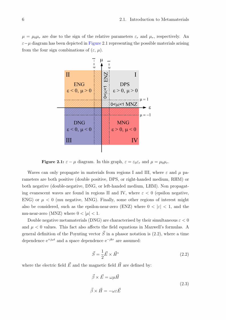
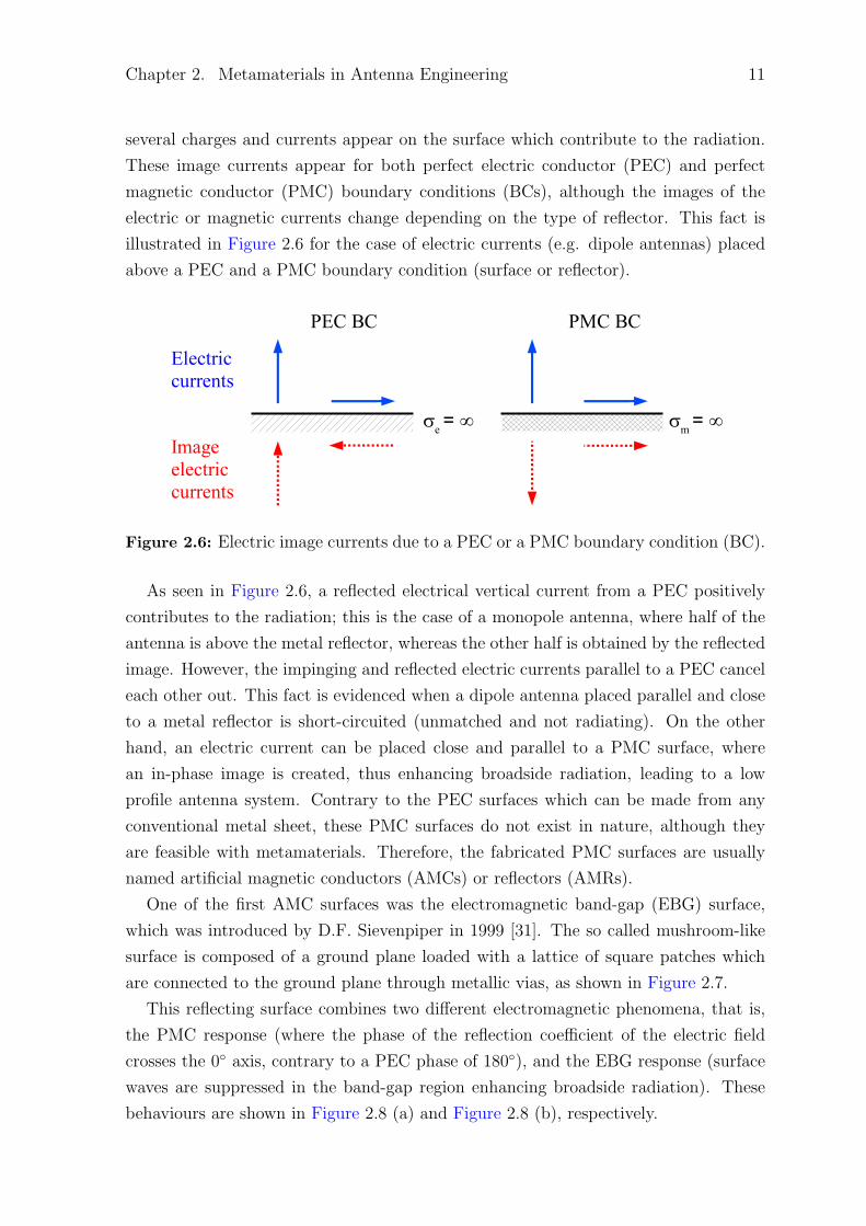
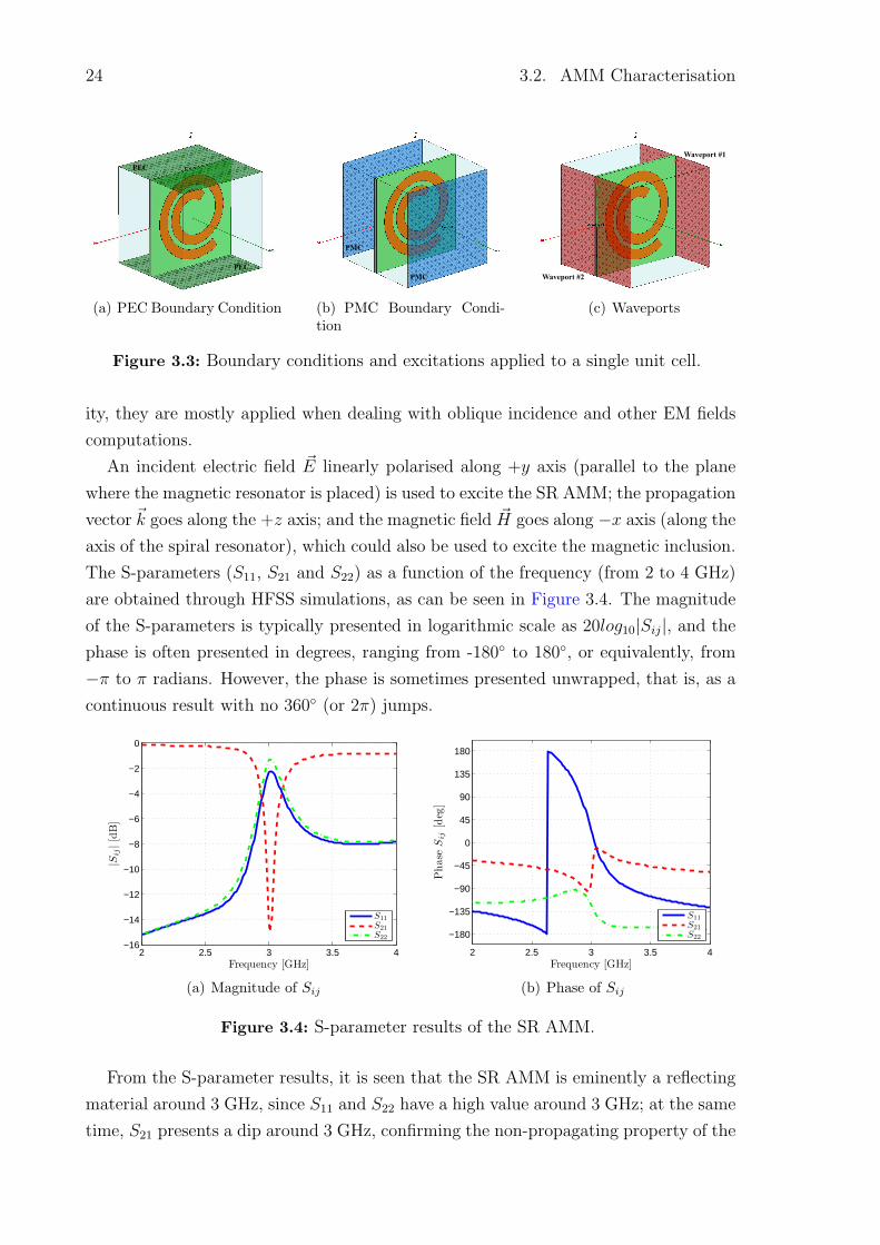
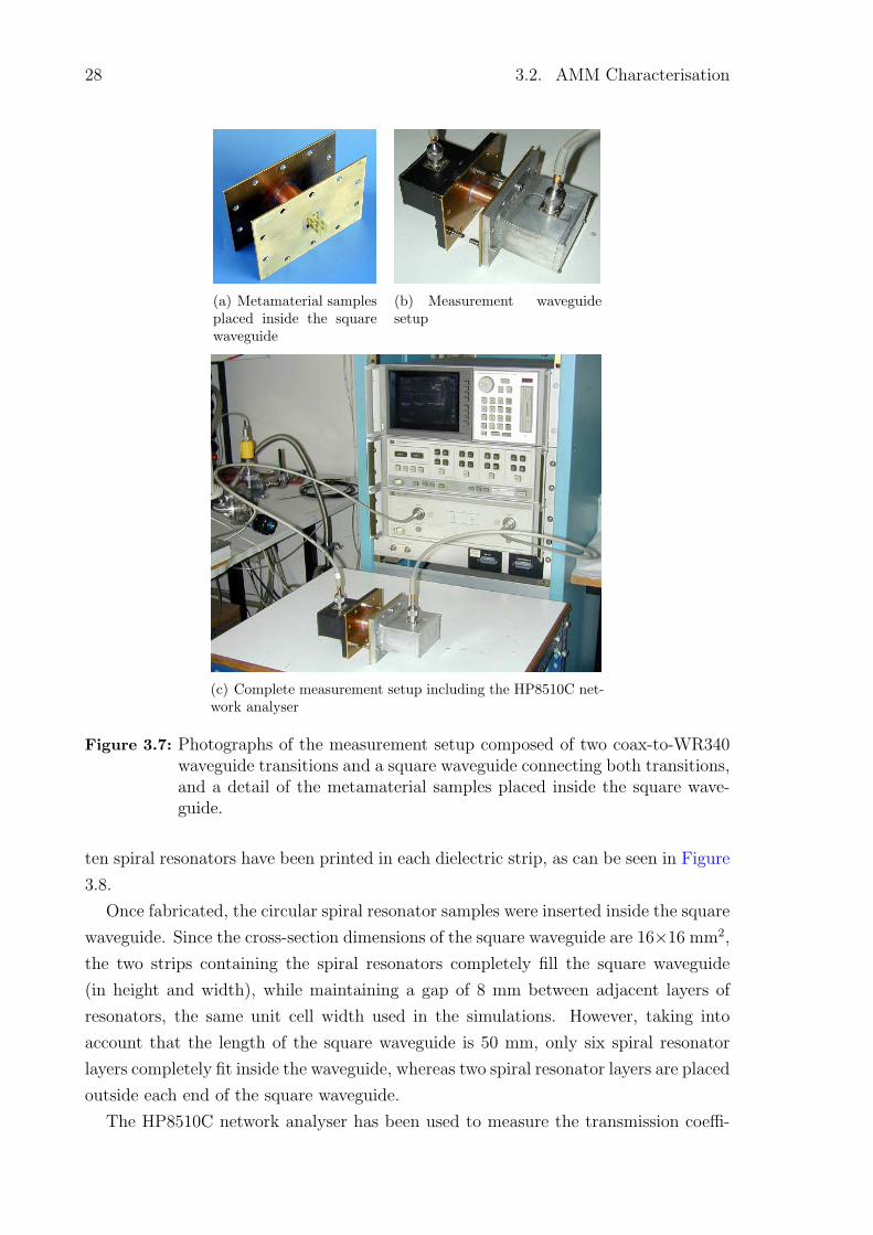
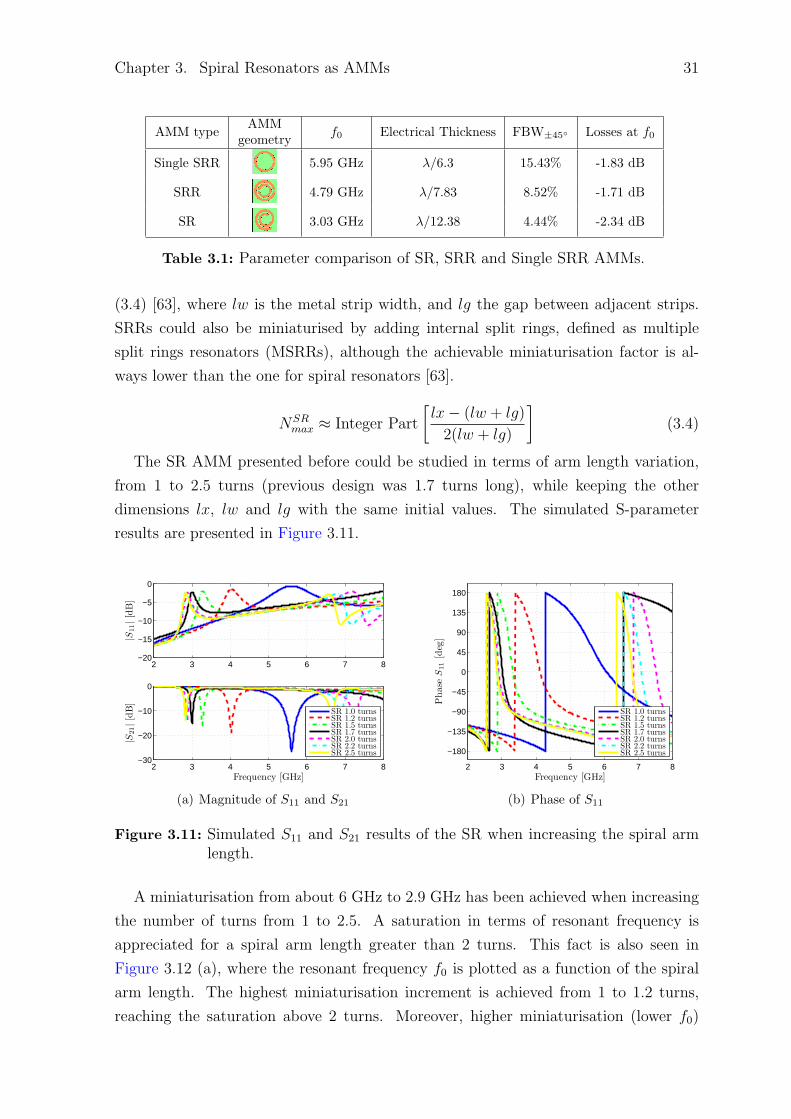
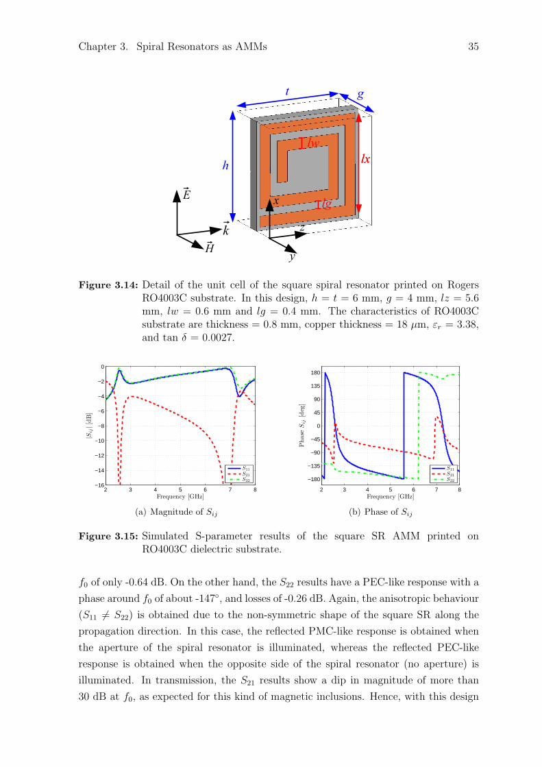
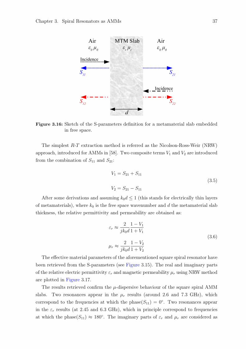
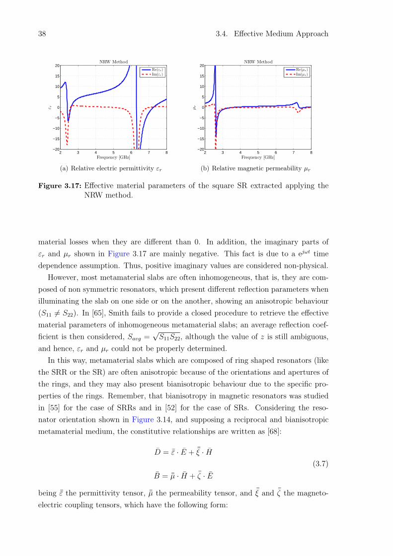
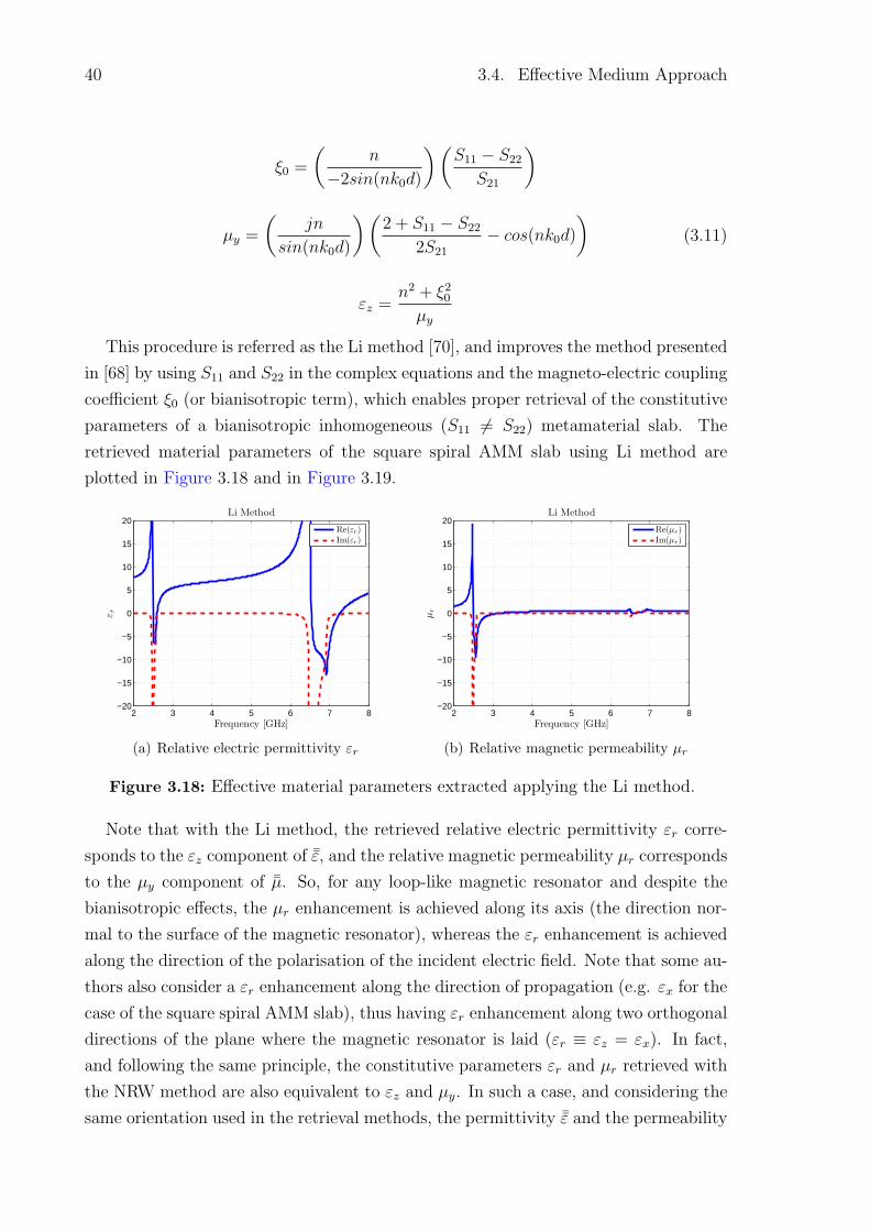
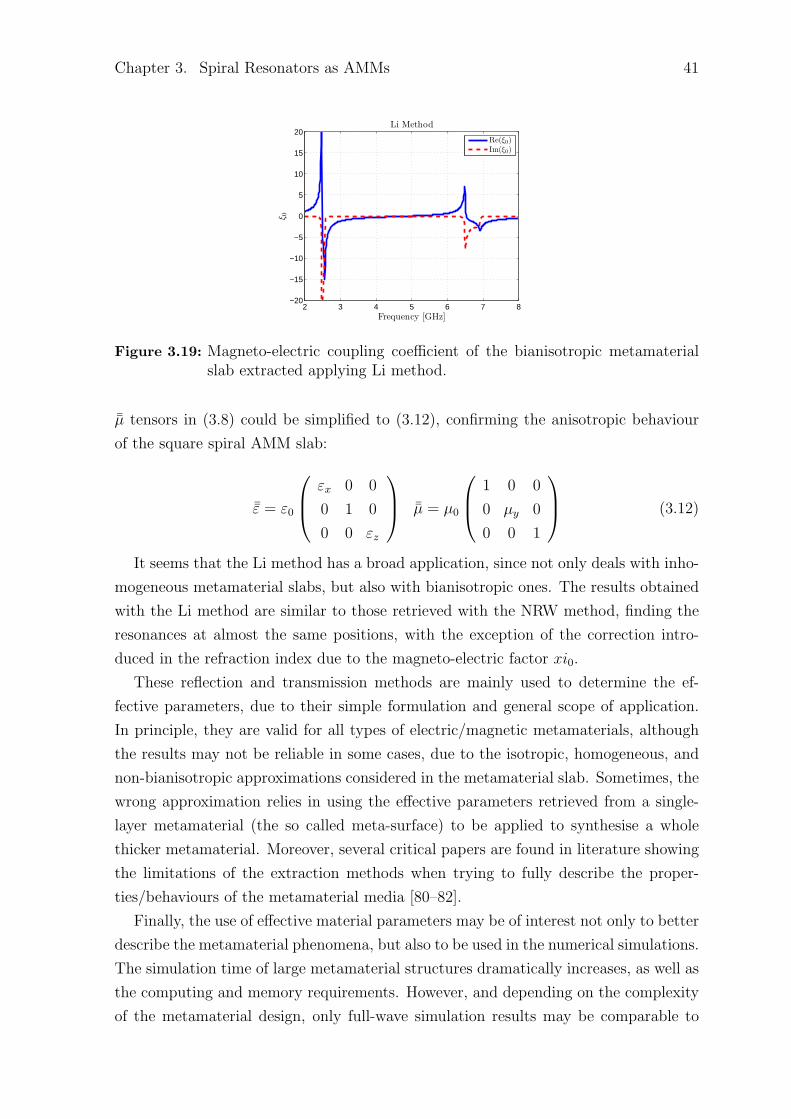
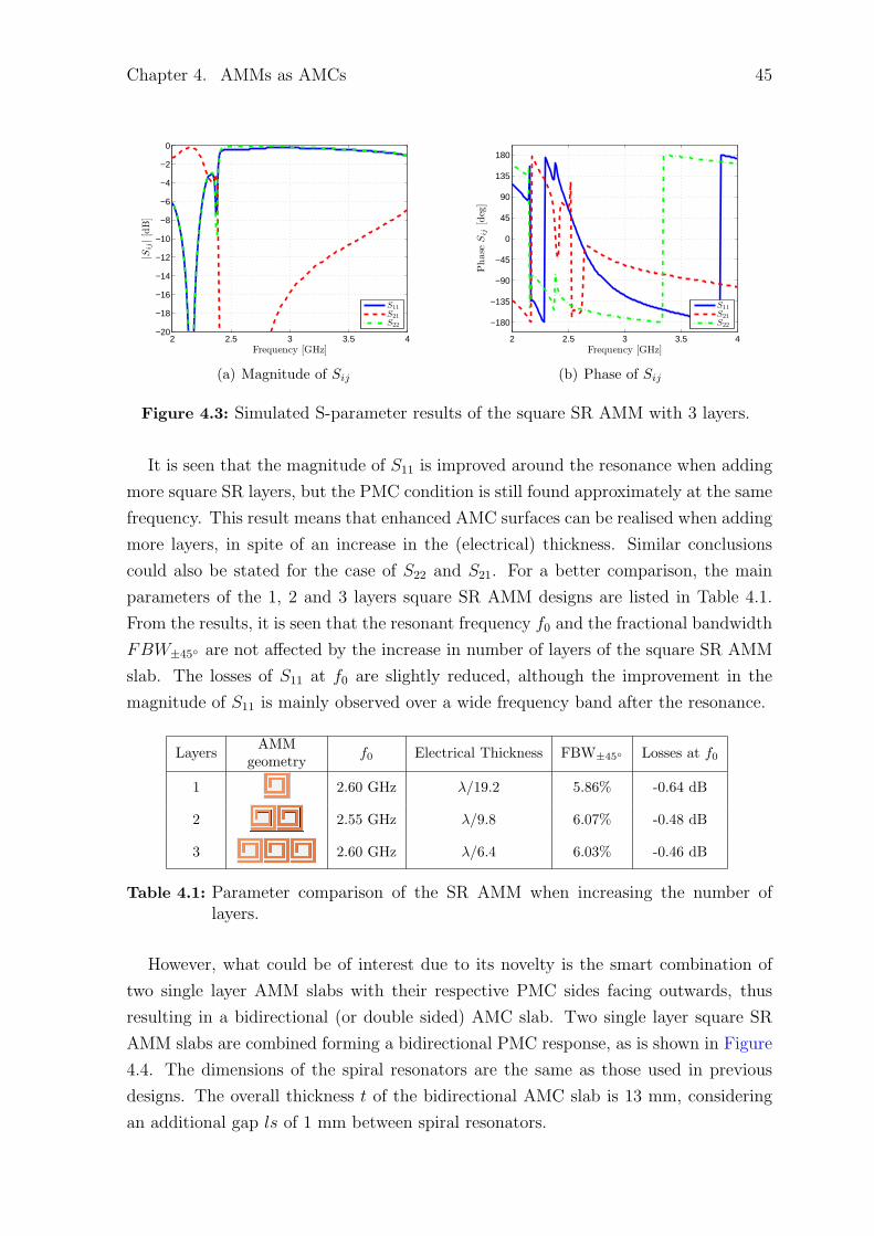
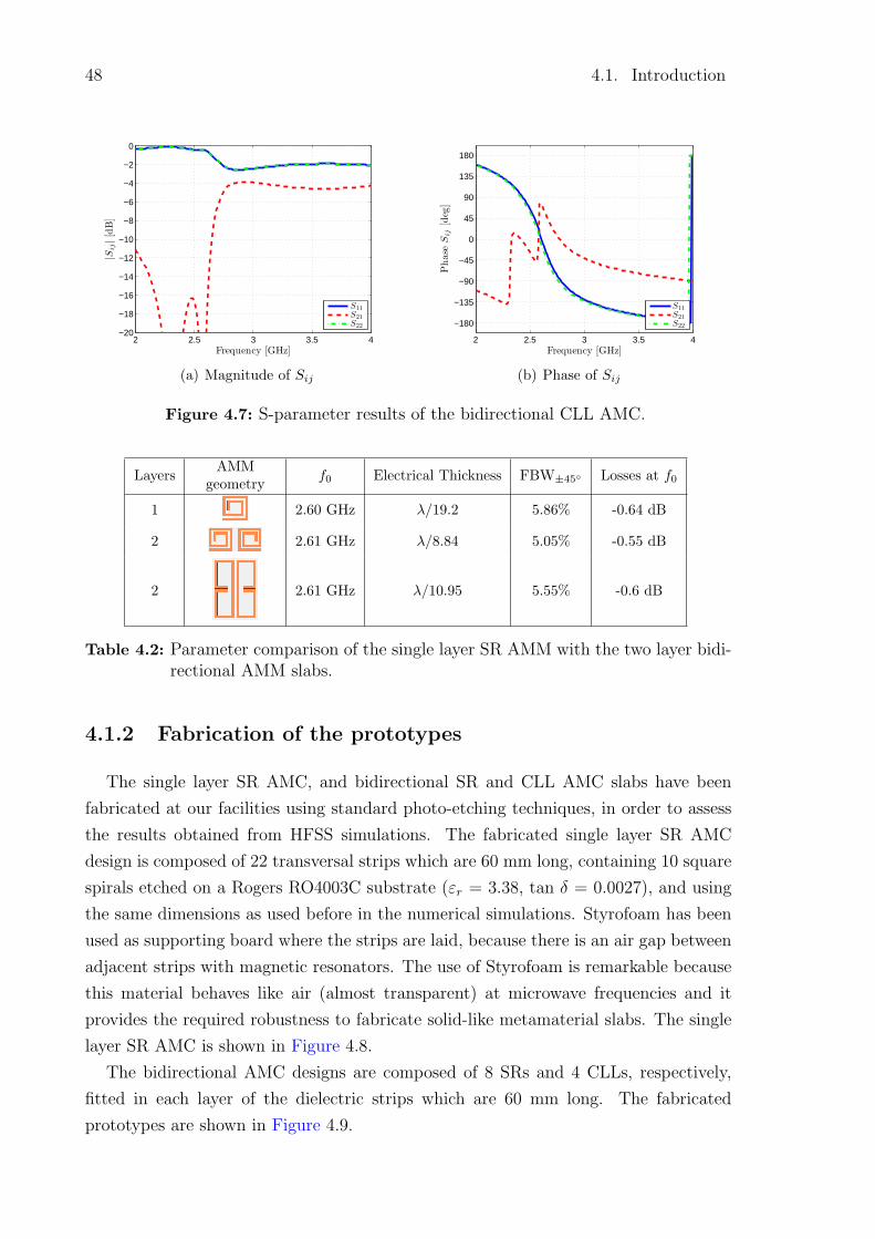
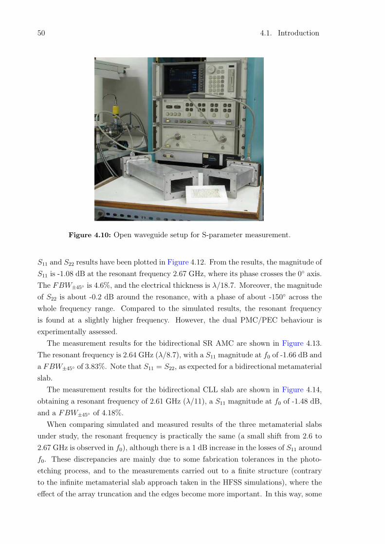
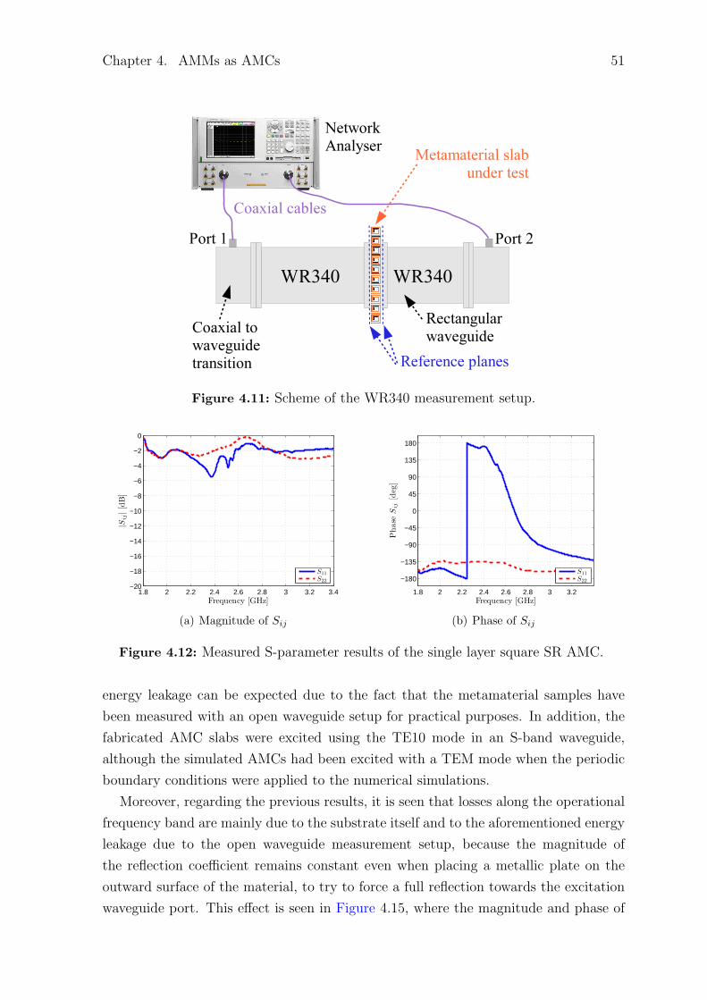
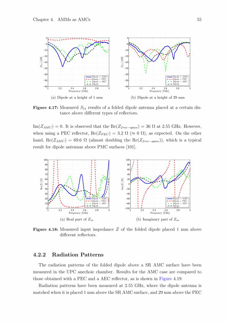
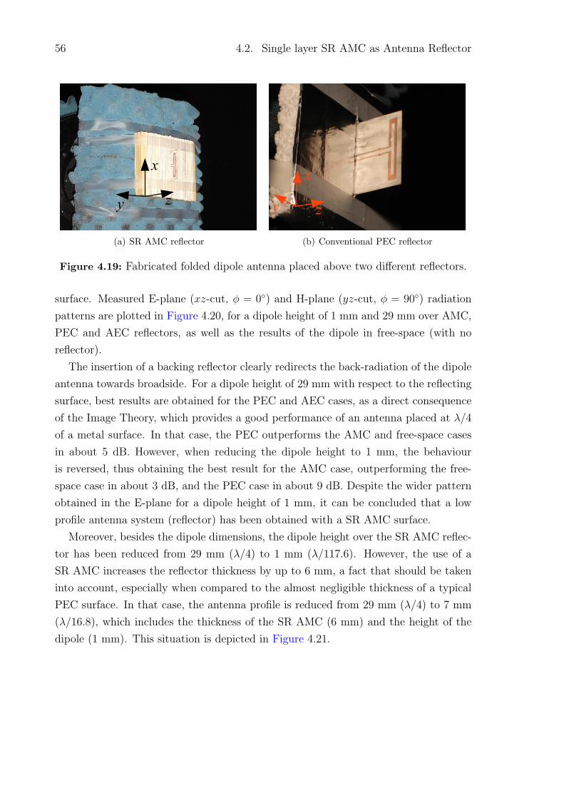
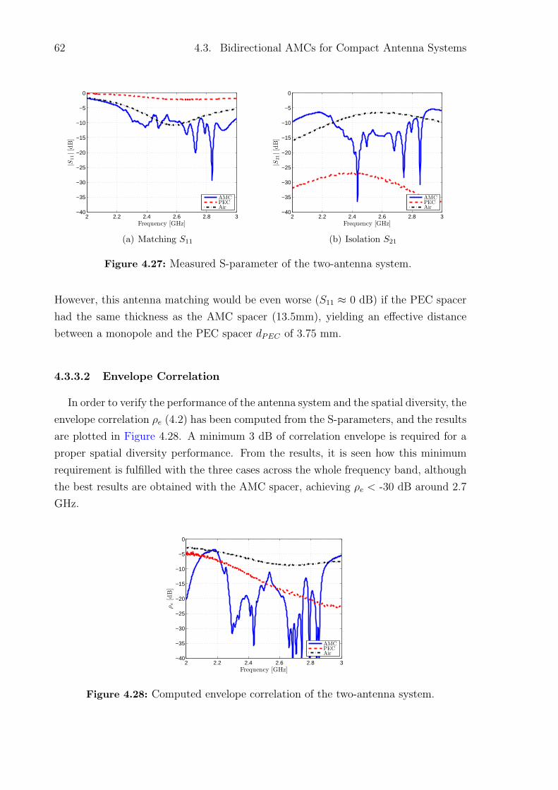
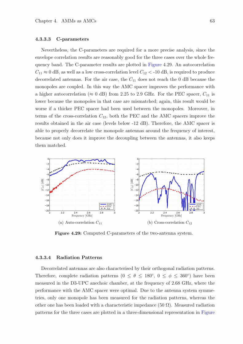
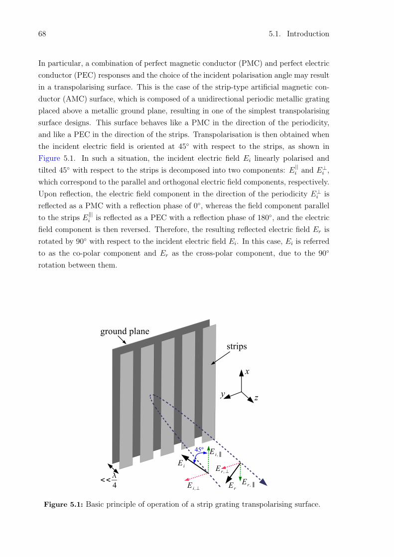
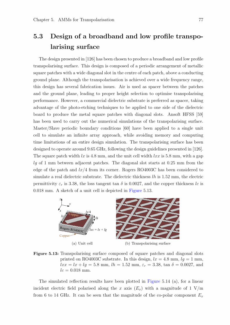
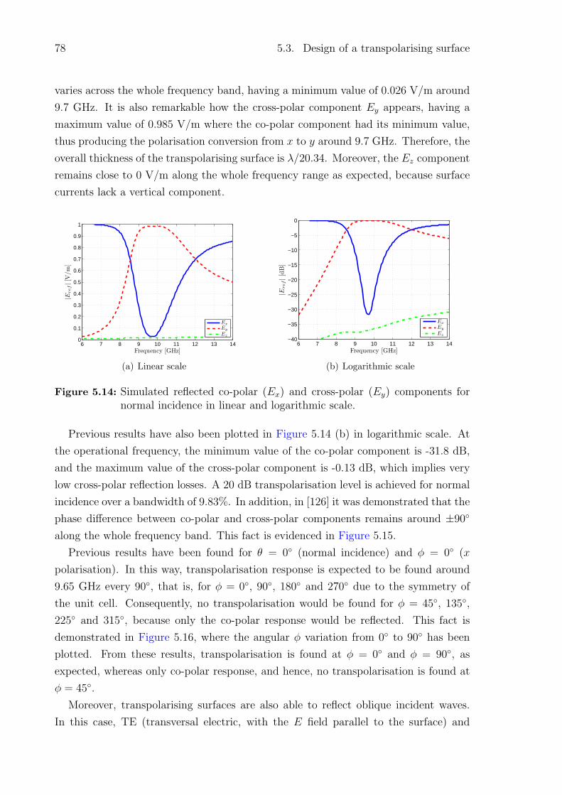
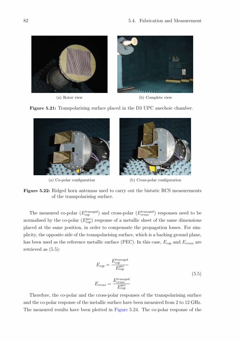
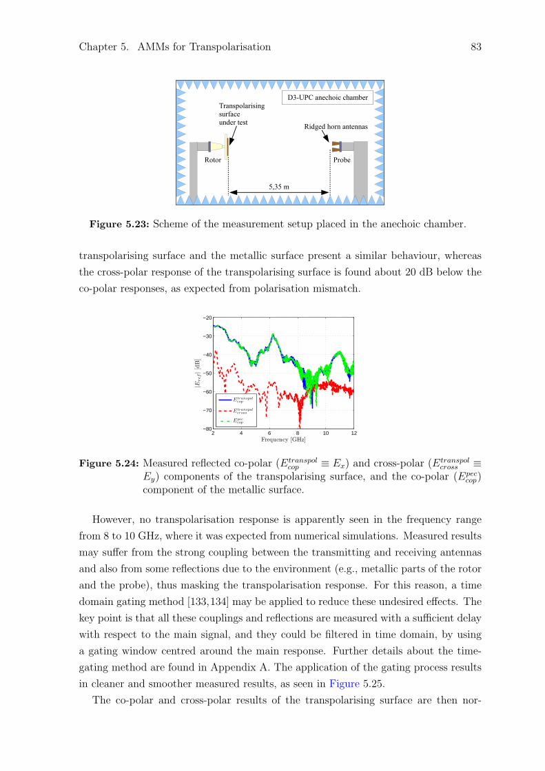
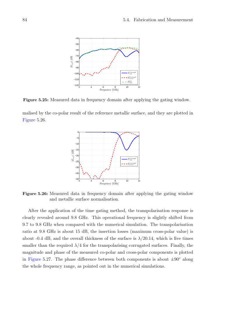
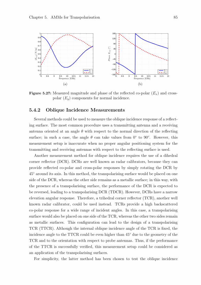
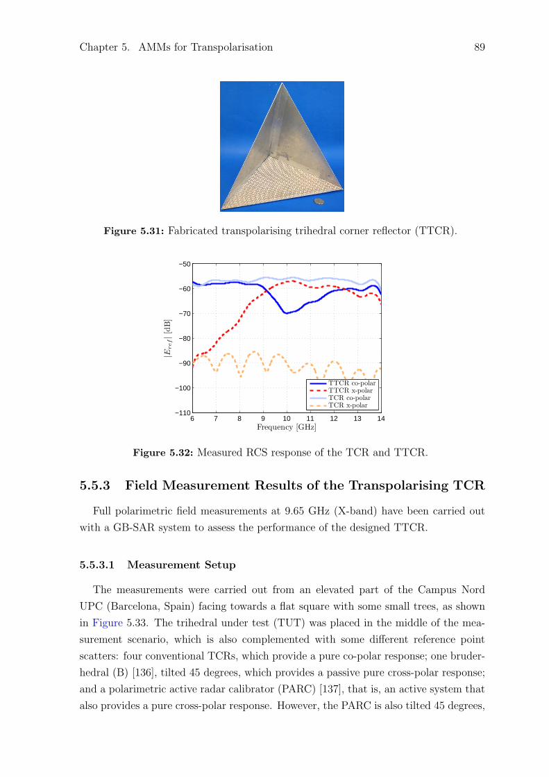
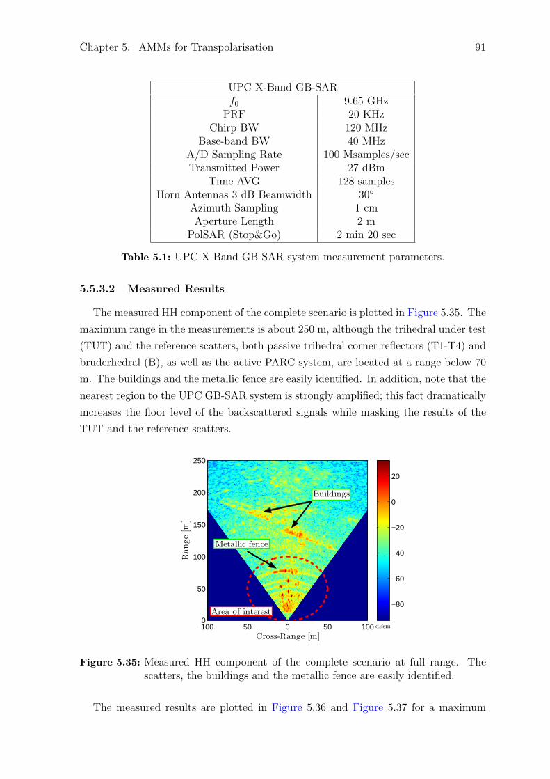
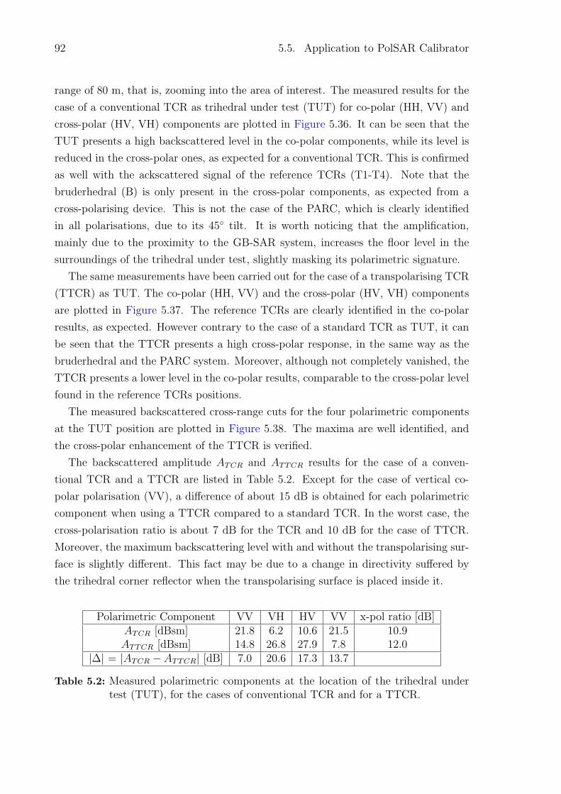
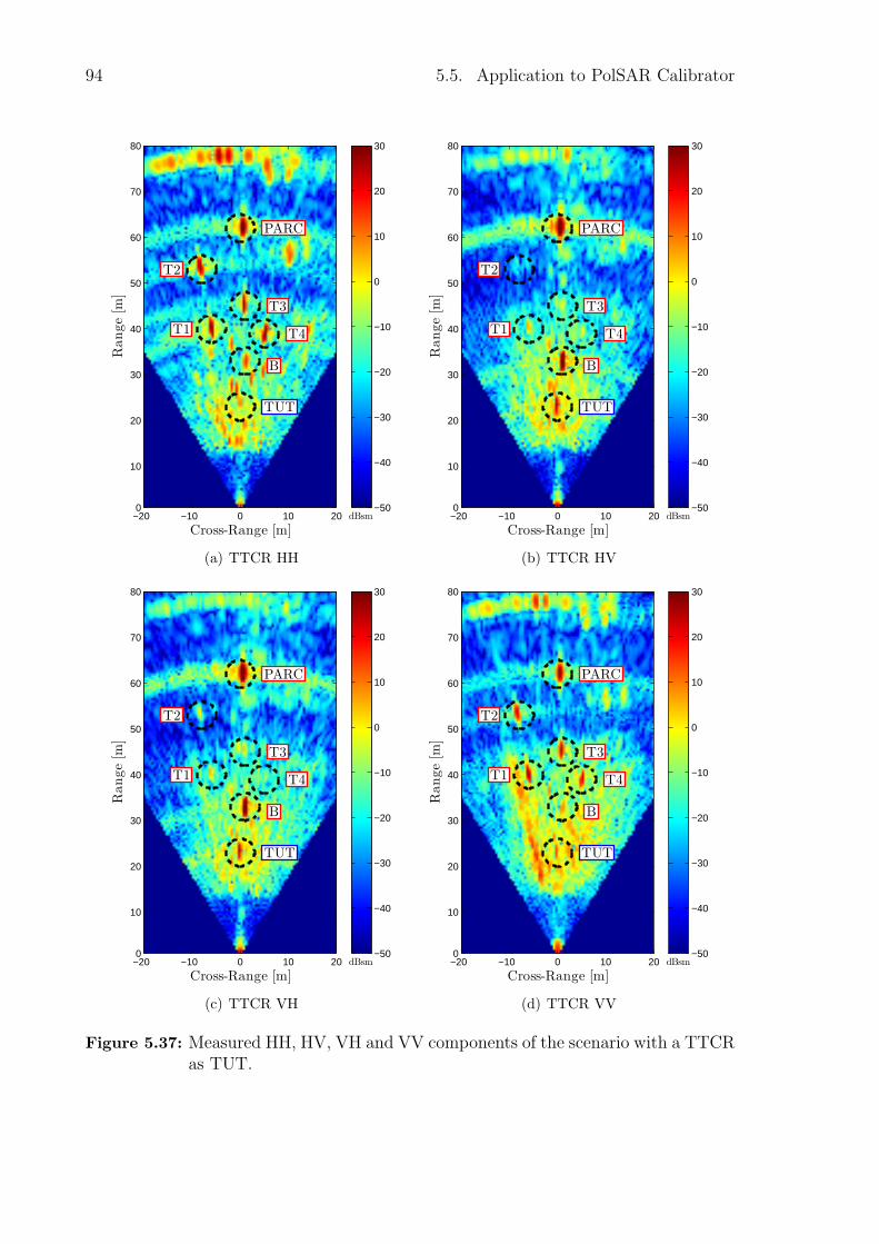
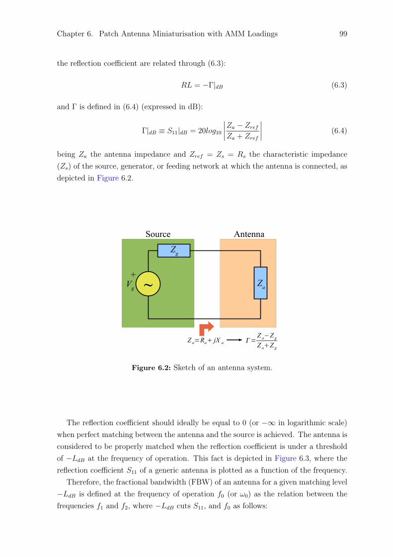
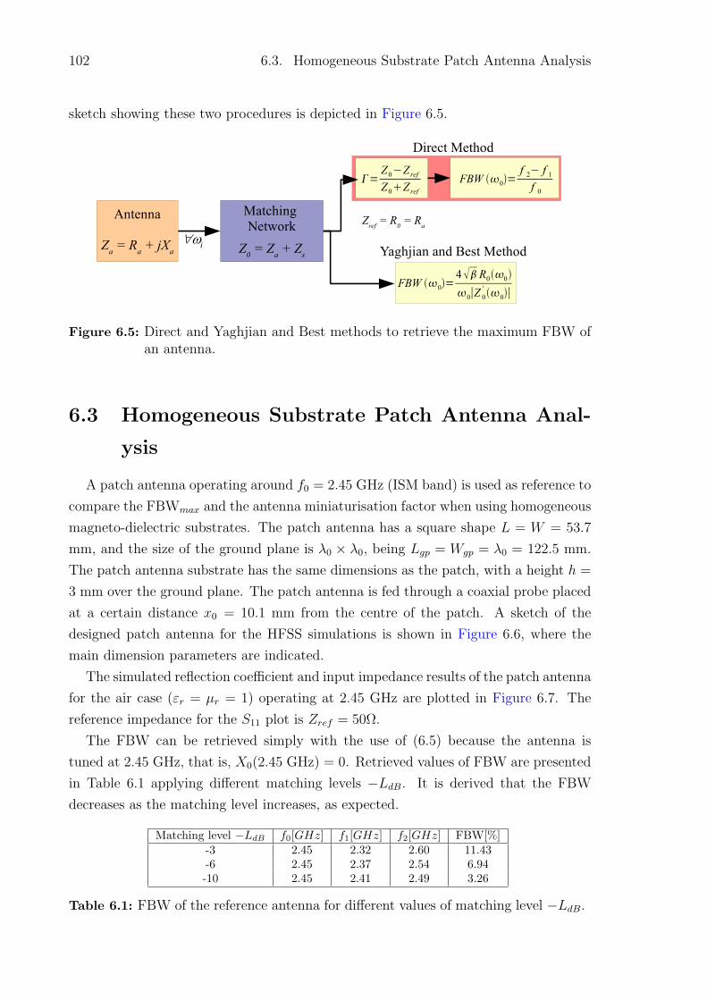
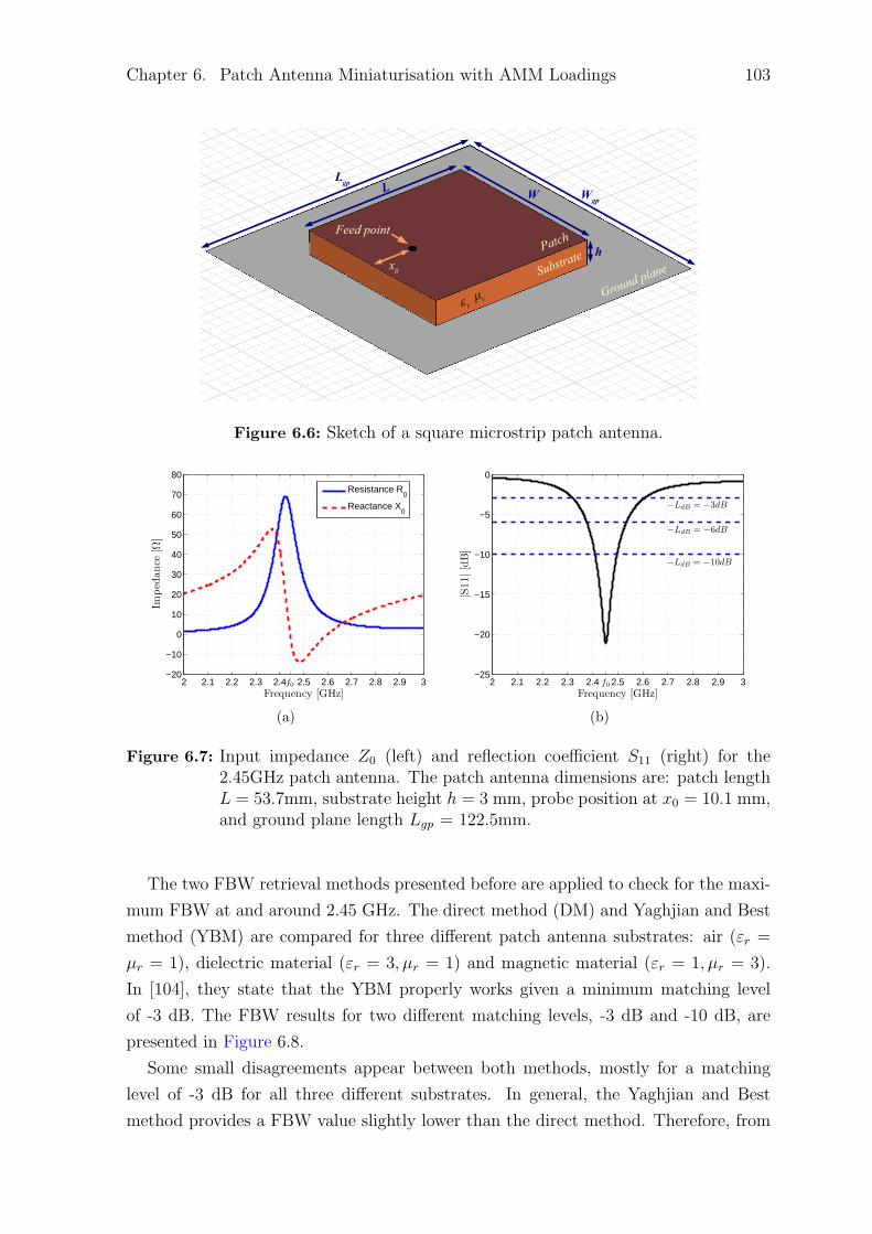
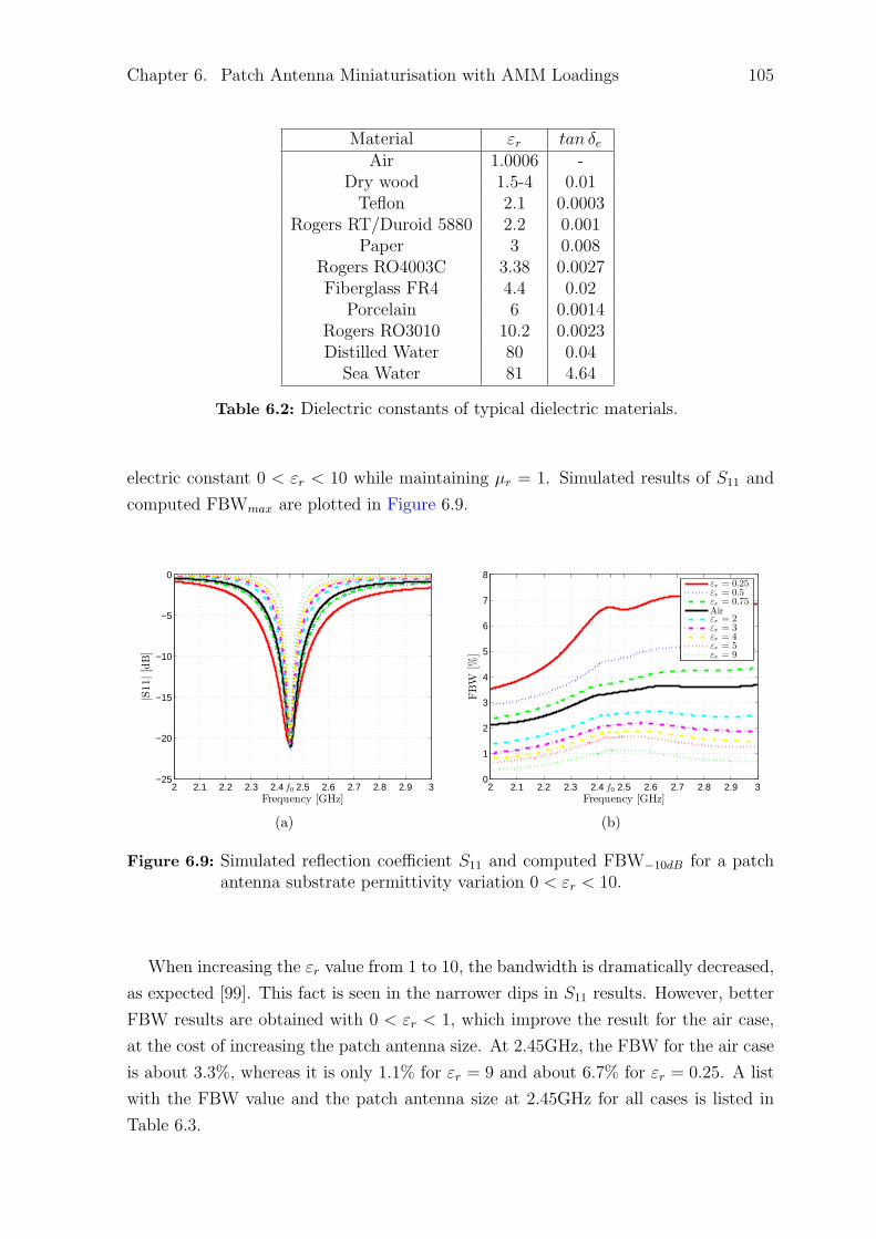
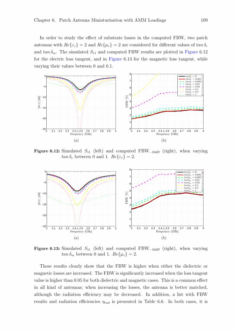
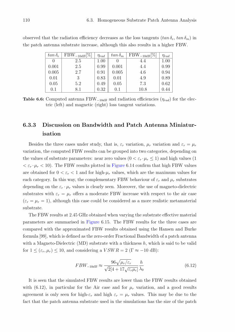
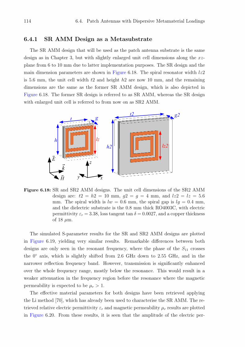
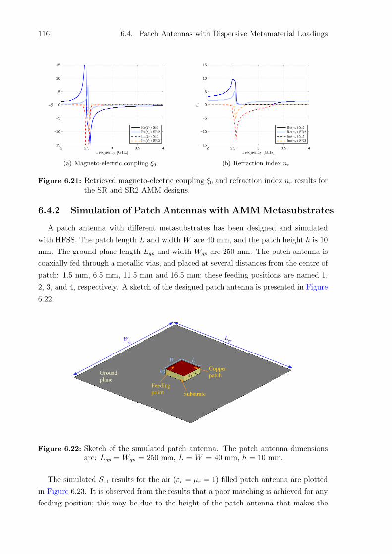
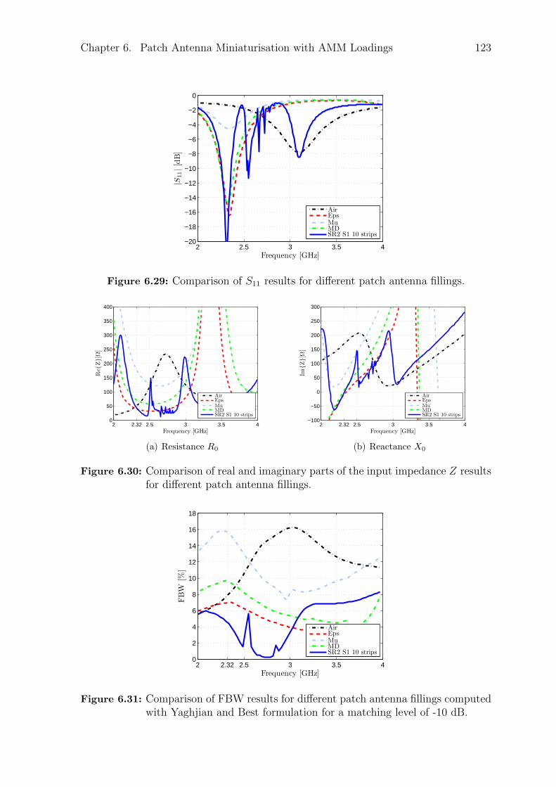
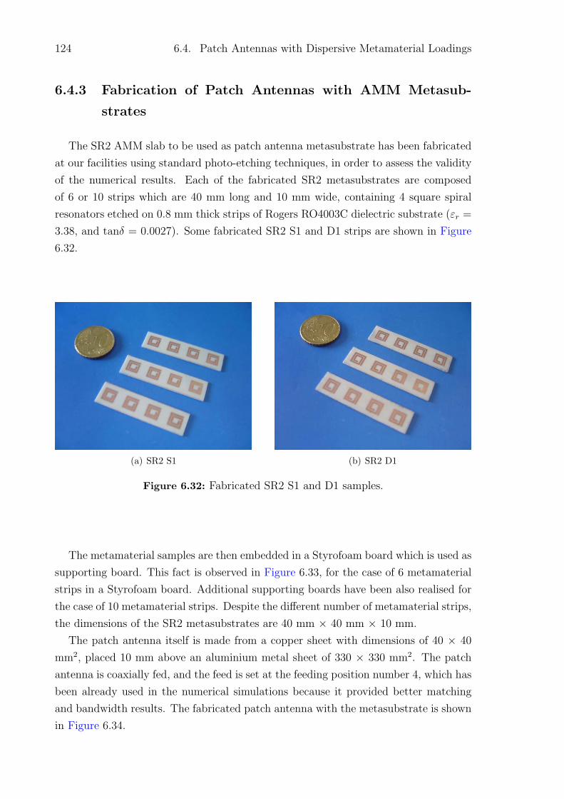
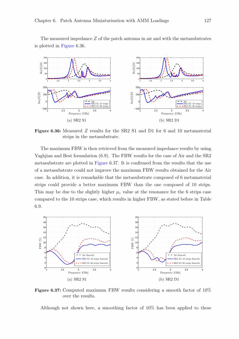
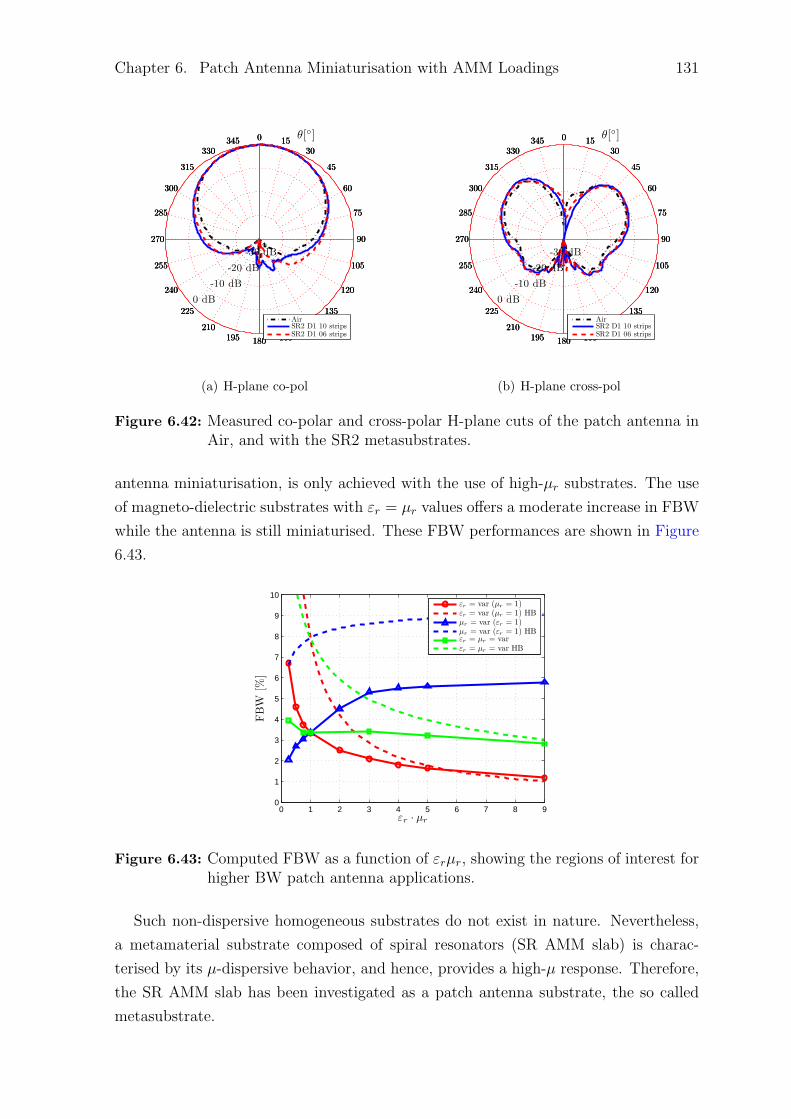
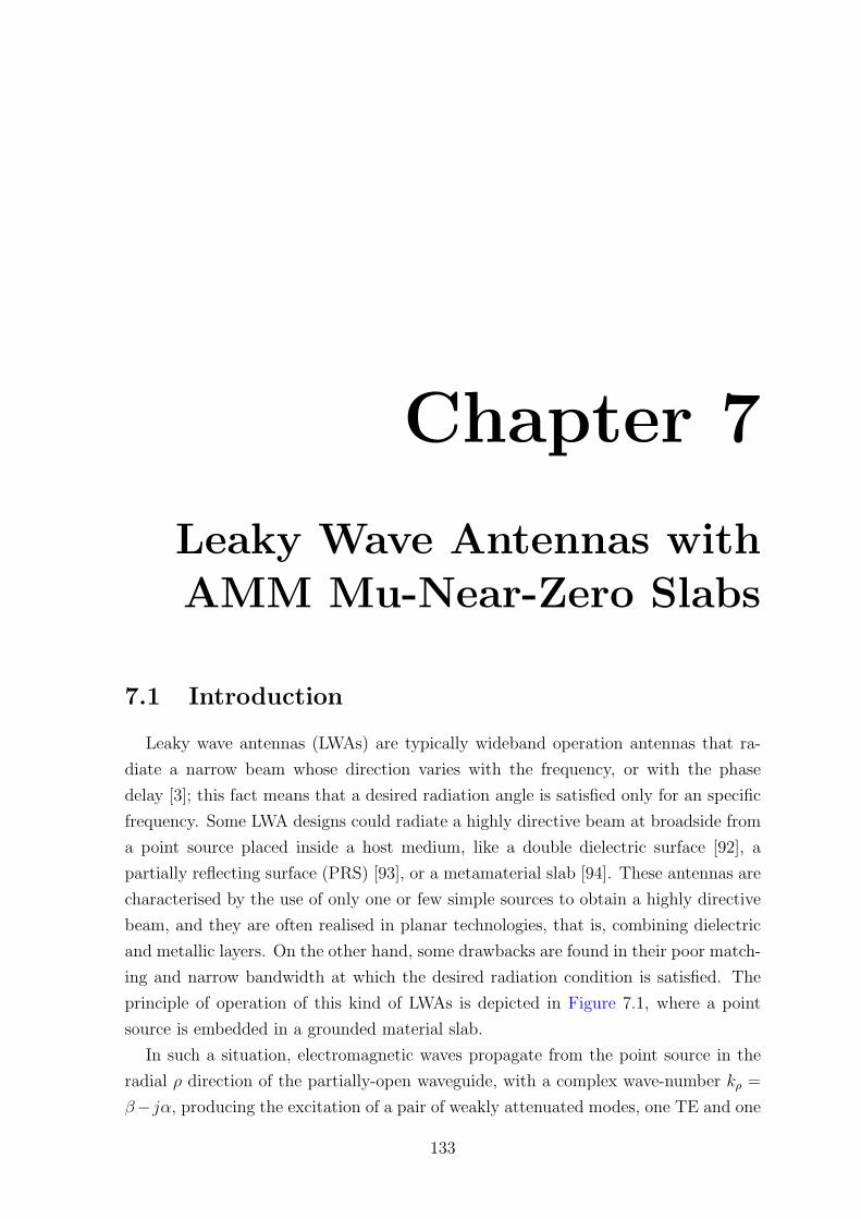
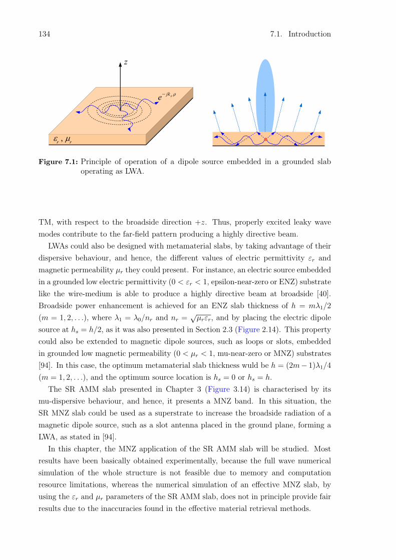
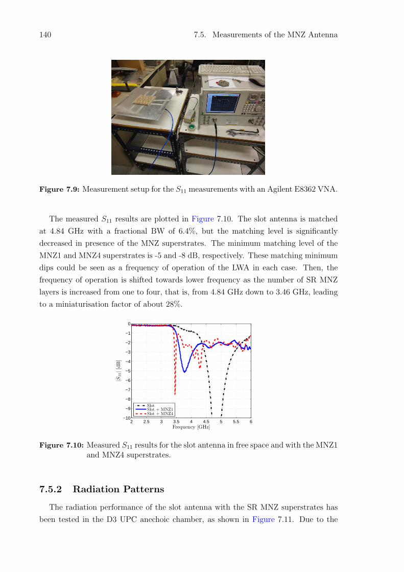
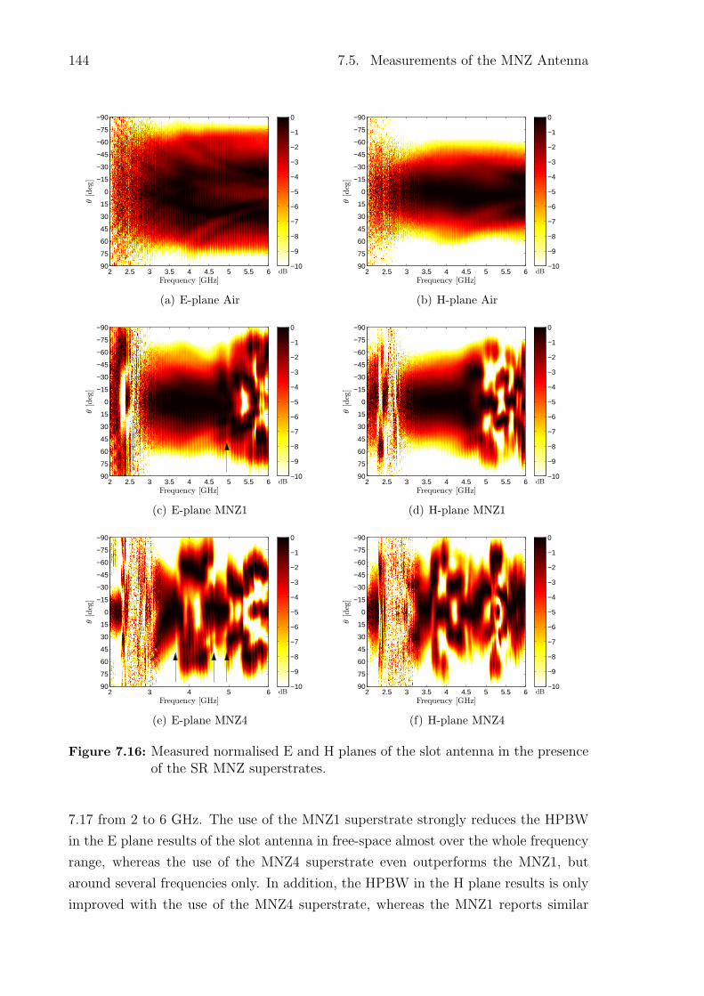
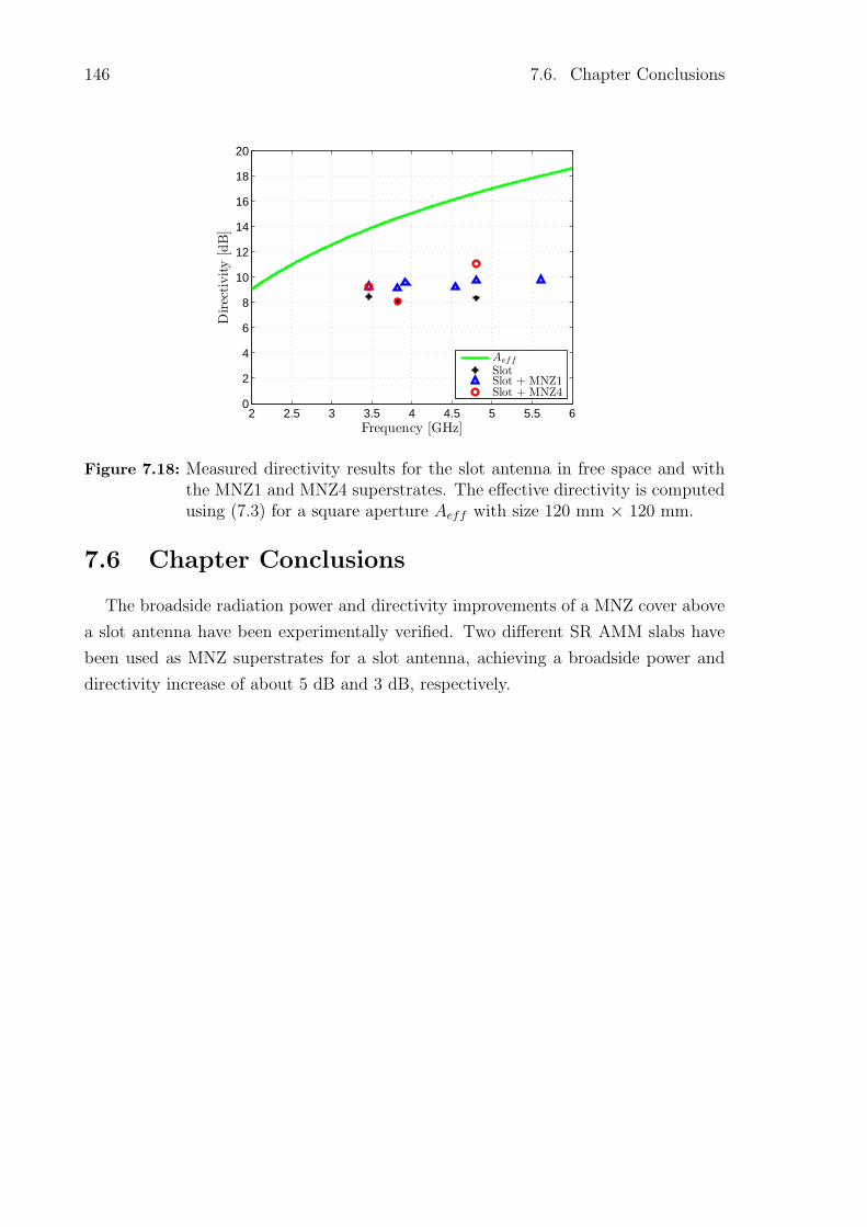
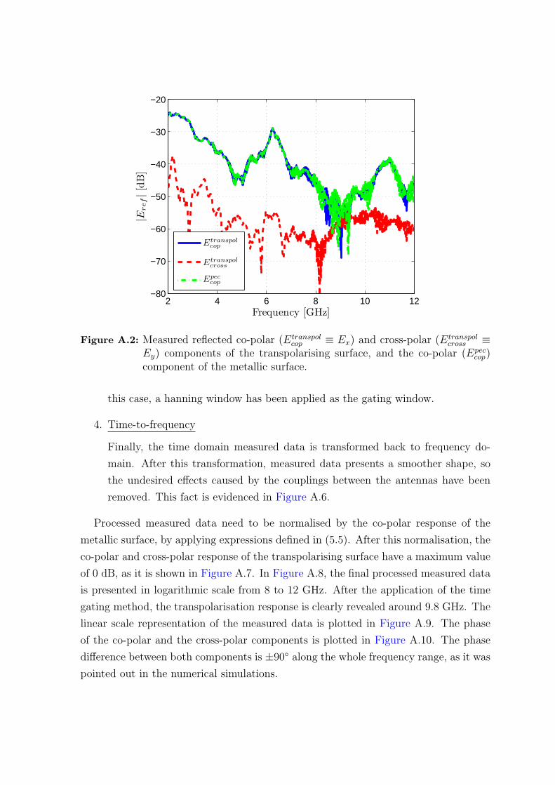
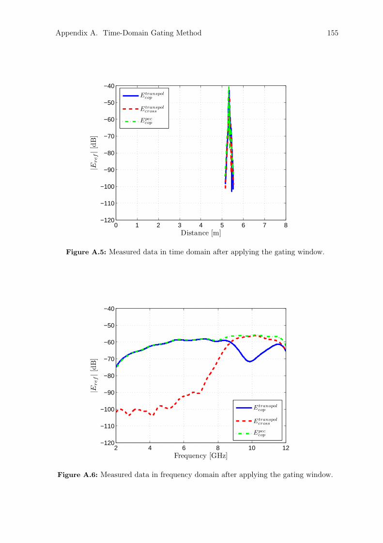
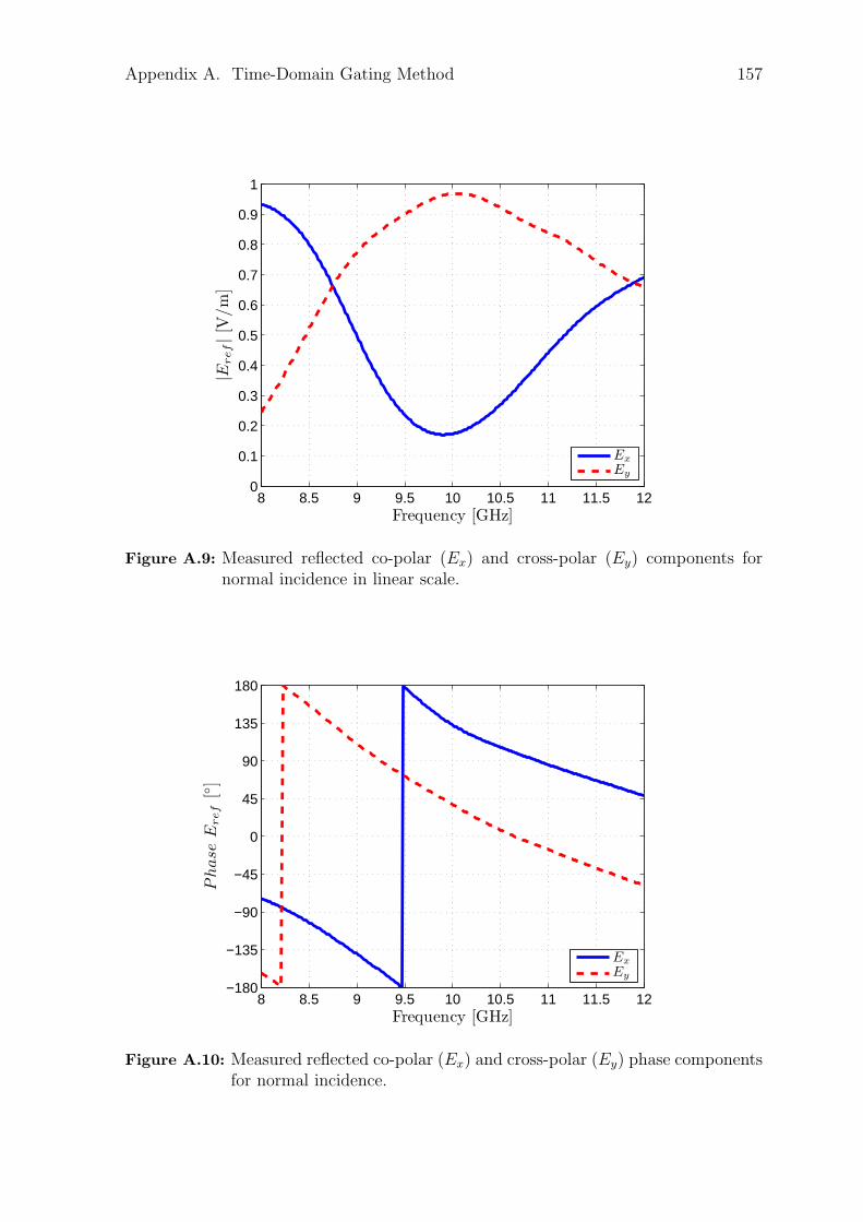
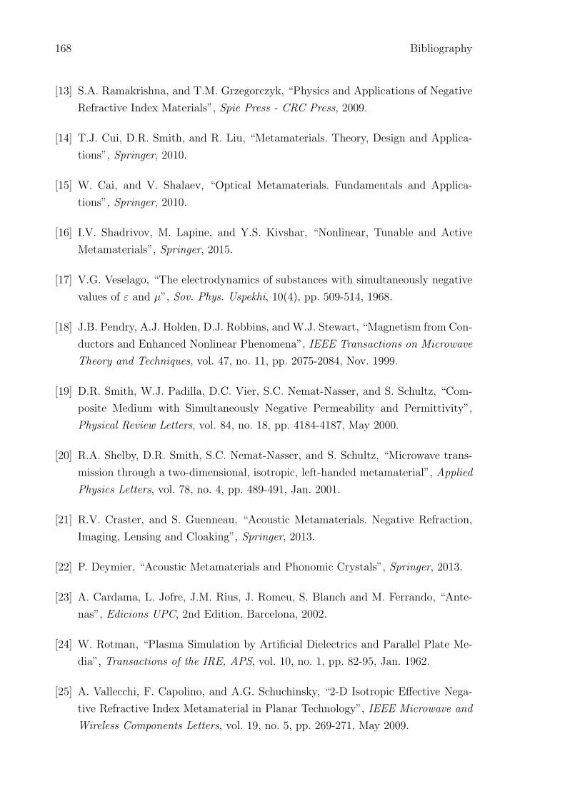
2 4 6 8 10 12−80
−70
−60
−50
−40
−30
−20
Frequency [GHz]
|Eref|[
dB
]
Etranspolcop
Etranspolcross
Epeccop
Figure A.2: Measured reflected co-polar (Etranspolcop ≡ Ex) and cross-polar (Etranspol
cross ≡Ey) components of the transpolarising surface, and the co-polar (Epec
cop)component of the metallic surface.
this case, a hanning window has been applied as the gating window.
4. Time-to-frequency
Finally, the time domain measured data is transformed back to frequency do-
main. After this transformation, measured data presents a smoother shape, so
the undesired effects caused by the couplings between the antennas have been
removed. This fact is evidenced in Figure A.6.
Processed measured data need to be normalised by the co-polar response of the
metallic surface, by applying expressions defined in (5.5). After this normalisation, the
co-polar and cross-polar response of the transpolarising surface have a maximum value
of 0 dB, as it is shown in Figure A.7. In Figure A.8, the final processed measured data
is presented in logarithmic scale from 8 to 12 GHz. After the application of the time
gating method, the transpolarisation response is clearly revealed around 9.8 GHz. The
linear scale representation of the measured data is plotted in Figure A.9. The phase
of the co-polar and the cross-polar components is plotted in Figure A.10. The phase
difference between both components is ±90 along the whole frequency range, as it was
pointed out in the numerical simulations.
154 Appendix A. Time-Domain Gating Method
2 4 6 8 10 12−120
−110
−100
−90
−80
−70
−60
−50
−40
Frequency [GHz]
|Eref|[
dB
]
Etranspolcop
Etranspolcross
Epeccop
Figure A.3: Measured data after applying empty chamber correction.
0 1 2 3 4 5 6 7 8−120
−110
−100
−90
−80
−70
−60
−50
−40
Distance [m]
|Eref|[
dB
]
Etranspolcop
Etranspolcross
Epeccop
Figure A.4: Measured data in time domain.
Appendix A. Time-Domain Gating Method 155
0 1 2 3 4 5 6 7 8−120
−110
−100
−90
−80
−70
−60
−50
−40
Distance [m]
|Eref|[
dB
]
Etranspolcop
Etranspolcross
Epeccop
Figure A.5: Measured data in time domain after applying the gating window.
2 4 6 8 10 12−120
−110
−100
−90
−80
−70
−60
−50
−40
Frequency [GHz]
|Eref|[
dB
]
Etranspolcop
Etranspolcross
Epeccop
Figure A.6: Measured data in frequency domain after applying the gating window.
156 Appendix A. Time-Domain Gating Method
2 4 6 8 10 12−40
−35
−30
−25
−20
−15
−10
−5
0
Frequency [GHz]
|Eref|[
dB
]
Etranspolcop
Etranspolcross
Figure A.7: Measured data in frequency domain after applying the metallic surfaceresponse normalisation.
8 8.5 9 9.5 10 10.5 11 11.5 12−40
−35
−30
−25
−20
−15
−10
−5
0
Frequency [GHz]
|Eref|[
dB
]
Ex
Ey
Figure A.8: Measured reflected co-polar (Ex) and cross-polar (Ey) components fornormal incidence in logarithmic scale.
Appendix A. Time-Domain Gating Method 157
8 8.5 9 9.5 10 10.5 11 11.5 120
0.1
0.2
0.3
0.4
0.5
0.6
0.7
0.8
0.9
1
Frequency [GHz]
|Eref|[
V/m
]
Ex
Ey
Figure A.9: Measured reflected co-polar (Ex) and cross-polar (Ey) components fornormal incidence in linear scale.
8 8.5 9 9.5 10 10.5 11 11.5 12−180
−135
−90
−45
0
45
90
135
180
Frequency [GHz]
Phase
Eref
[]
Ex
Ey
Figure A.10: Measured reflected co-polar (Ex) and cross-polar (Ey) phase componentsfor normal incidence.
Appendix B
List of Publications
The work presented in this thesis has contributed to the publication of several in-
ternational peer-reviewed article and conference papers.
Book Chapters
1. P.J. Ferrer, J.M. Gonzalez-Arbesu, J. Romeu, J. Parron, G. Junkin, and R.
Villarino, “Small and Multiband MNG Resonators: Spiral, Pre-fractal and Other
Geometries”, Handbook on Artificial Materials, F. Capolino, Ed., CRC Press,
2009.
Journals
1. P.J. Ferrer, B. Kelem, and C. Craeye, “Design of Broadband Transpolarising
Surfaces”, Microwave and Optical Technology Letters, vol. 48, no. 12, pp. 2606-
2611, Dec. 2006.
2. P.J. Ferrer, J.M. Gonzalez-Arbesu, J. Romeu, and A. Cardama, “Bidirectional
Artificial Magnetic Reflectors at Microwave Frequencies”, Microwave and Optical
Technology Letters, vol. 49, no. 8, pp. 1949-1953, Aug. 2007.
159
160 Appendix B. List of Publications
3. P.J. Ferrer, J.M. Gonzalez-Arbesu, and J. Romeu, “Decorrelation of two closely
spaced antennas with a Metamaterial AMC Surface”, Microwave and Optical
Technology Letters, vol. 50, no. 5, pp. 1414-1417, May 2008.
4. P.J. Ferrer, C. Lopez-Martınez, A. Aguasca, L. Pipia, J.M. Gonzalez-Arbesu, X.
Fabregas, and J. Romeu, “Transpolarising Trihedral Corner Reflector Character-
isation Using a GB-SAR System”, IEEE Geoscience and Remote Sensing Letters,
vol. 8, no. 4, pp. 774-778, Jul. 2011.
5. M. Imbert, P.J. Ferrer, J.M. Gonzalez-Arbesu, and J. Romeu, “Assessment of
the Performance of a Metamaterial Spacer in a Closely Spaced Multiple-Antenna
Syste”, IEEE Antennas and Wireless Propagation Letters, pp. 720-723, Jun.
2012.
Conferences
1. B. Kelem, P.J. Ferrer, and C. Craeye, “Design of Broadband Transpolarising
Surfaces”, Proceedings of 3rd Workshop Metamaterials 2006, Roma (Italy), 30-
31 March 2006.
2. P.J. Ferrer, J.M. Gonzalez-Arbesu, and J. Romeu, “Design and measurement of
a Spiral-Cell PMC for Metamaterial Applications”, Proceedings of the IEEE AP-
S/URSI 2006 International Sysmposium (AP-S 2006), Albuquerque (USA), 9-14
Jul. 2006.
3. P.J. Ferrer, F. Fortuny, J.M. Gonzalez-Arbesu, and J. Romeu, “Desings for Bifre-
quency and Bidirectional AMC Surfaces”, Proceedings of the 1st European Con-
ference on Antennas and Propagation (EuCAP 2006), Nice (France), 6-10 Nov.
2006.
4. P.J. Ferrer, J.M. Gonzalez-Arbesu, and J. Romeu, “Bidirectional Metamaterial
Separator for Compact Antenna Systems”, Proceedings of the IEEE Antennas
and Propagation Symposium (AP-S 2007), Honolulu (USA), 9-15 June 2007.
5. P.J. Ferrer, C. Lopez-Martınez, X. Fabregas, J.M. Gonzalez-Arbesu, J. Romeu,
A. Aguasca, and C. Craeye, “Transpolarizing Surfaces for Polarimetric SAR Sys-
tems Calibration”, Proceedings of the IEEE International Geoscience and Remote
Sensing Symposium (IGARSS 2007), Barcelona (Spain), 23-28 Jul. 2007.
6. P.J. Ferrer, J.M. Gonzalez-Arbesu, J. Romeu, and C. Craeye, “Design and Fabri-
cation of Transpolarising Surfaces”, Proceedings of the 14th International Student
Seminar (ISS 2007), Belfast (UK), August 2007.
Appendix B. List of Publications 161
7. P.J. Ferrer, J.M. Gonzalez-Arbesu, and J. Romeu, “Metamaterial slabs with dou-
ble side PMC response”, Proceedings of the 1st International Congress on Ad-
vanced Electromagnetic Materials in Microwaves and Optics (Metamaterials’07),
Roma (Italy), 22-26 Oct. 2007.
8. P.J. Ferrer, J.M. Gonzalez-Arbesu, J. Romeu, and C. Craeye, “Design and Fab-
rication of a Cross-polarising AMC Surface”, Proceedings of the 2nd European
Conference on Antennas and Propagation (Eucap 2007), Edinburgh (UK), 11-16
Nov. 2007.
9. P.J. Ferrer, J. Romeu, J.M. Gonzalez-Arbesu, and J. Parron, “Broadside Radia-
tion Enhancement Using MNZ Substrate”, Proceedings of the 2nd Young Scientist
Meeting on Metamaterials 2008 (YSMM’08), Barcelona (Spain), 5-8 Feb. 2008.
10. P.J. Ferrer, J. Romeu, J.M. Gonzalez-Arbesu, J. Parron, F. Capolino, F. Bilotti,
L. Vegni, G. Lovat, and P. Burghignoli, “Broadside Radiation Enhancement Us-
ing a Spiral Resonator MNZ Metamaterial Substrate”, Proceedings of the IEEE
Antennas and Propagation Symposium (AP-S 2008), San Diego, CA (USA), 5-11
Jul. 2008.
11. P.J. Ferrer, I. Calafell, J.M. Gonzalez-Arbesu, and J. Romeu, “Bandwidth and
Size Behaviour Study for Patch Antennas using Metamaterial Fillings with Posi-
tive Permittivity and Permeability”, Proceedings of the 2nd International Congress
on Advanced Electromagnetic Materials in Microwaves and Optics (Metamateri-
als’08), Pamplona (Spain), 21-26 Sept. 2008.
12. P.J. Ferrer, J.M. Gonzalez-Arbesu, C. Craeye, and J. Romeu, “Transpolariz-
ing surfaces and potential applications”, Proceedings of the European Microwave
Conference (EuMC 2008), Amsterdam (The Netherlands), 27-31 Oct. 2008.
13. P.J. Ferrer, J. Romeu, J.M. Gonzalez-Arbesu, A. Aguasca, L. Pipia, C. Lopez-
Martınez, and X. Fabregas, “Transpolarizing Trihedral Measurement Using UPC
X-BAND GBSAR”, Proceedings of the IEEE International Geoscience and Re-
mote Sensing Symposium (IGARSS 2009), Cape Town (South Africa), 12-17 Jul.
2009.
14. P.J. Ferrer, J.M. Gonzalez-Arbesu, and J. Romeu, “Spiral resonator Mu-Near-
Zero Substrates for Grounded Slot Antennas”, Proceedings of the European Con-
ference on Antennas and Propagation (Eucap 2010), Barcelona (Spain), 12-16
April 2010.
162 Appendix B. List of Publications
15. I. Calafell, P.J. Ferrer, J.M. Gonzalez-Arbesu, and J. Romeu, “Microstrip Patch
Antenna Design Using Artificial Material Loadings”, Proceedings of the European
Conference on Antennas and Propagation (Eucap 2010), Barcelona (Spain), 12-
16 April 2010.
16. M. Imbert, P.J. Ferrer, J.M. Gonzalez-Arbesu, and J. Romeu, “Design of a Bidi-
rectional Metamaterial Spacer at 2.45 GHz”, Proceedings of the European Con-
ference on Antennas and Propagation (Eucap 2010), Barcelona (Spain), 12-16
April 2010.
Invited Talks
1. P.J. Ferrer, J.M. Gonzalez-Arbesu, and J. Romeu, “Metamaterial Applications
to Antenna Design”, Workshop on Aplicaciones de los Metamateriales en cir-
cuitos, antenas y subsistemas de microondas, milimetricas y fotonicos, XXII
URSI, Tenerife, 19-21 Sep. 2007.
2. P.J. Ferrer, J.M. Gonzalez-Arbesu, and J. Romeu, “Review on Artificial Mag-
netic Materials for Antenna Applications”, Proceedings of the 3rd Young Scientist
Meeting on Metamaterials 2009 (YSMM’09), Leganes (Spain), 6-8 July 2009.
Supervised Master Thesis
1. I. Calafell, “Microstrip patch antenna design with artificial material loadings”,
ETSETB, TSC, UPC, Feb. 2009.
2. M. Imbert, “Disseny d’una pantalla bidireccional AMC per a un sistema compacte
d’antenes a 2.45 GHz”, ETSETB, TSC, UPC, May 2010.
Appendix C
List of Acronyms
AEC Artificial Electric Conductor
AER Artificial Electric Reflector
AMC Artificial Magnetic Conductor
AMM Artificial Magnetic Material
AMR Artificial Magnetic Reflector
B Bruderhedral
BC Boundary Condition
BC-SRR Broadside-Coupled SRR
BW Bandwidth
CLL Capacitively Loaded Loop (resonator)
CP Circular Polarisation
CRLH-TL Composite Right-Left-Handed Transmission Line
DCR Dihedral Corner Reflector
163
164 Appendix C. List of Acronyms
DGS Defected Ground Structure
DM Direct Maximum FBW Method
DNG Double Negative (resonator/medium/media)
DPS Double Positive (resonator/medium/media)
ENG Epsilon Negative (resonator/medium/media)
ENZ Epsilon-Near-Zero (resonator/medium/media)
FBW Fractional Bandwidth
GB-SAR Ground-Based SAR
HIS High Impedance Surface
HPBW Half Power Beam-Width
ISM Industrial, Scientific and Medical radio band
JGM Johnston-Geissler Method
LHM Left-Handed medium/media
LH-TL Left-Handed Transmission Line
LP Linear Polarisation
LWA Leaky Wave Antenna
MD Magneto-Dielectric
MDPA Magneto-Dielectric Patch Antenna
MEA Multiple Element Antenna
MIMO Multiple Input Multiple Output
MNG Mu Negative (resonator/medium/media)
MNZ Mu-Near-Zero (resonator/medium/media)
MSRR Multiple SRR
MTM Metamaterial
MPA Microstrip Patch Antenna
Appendix C. List of Acronyms 165
PARC Polarimetric Active Radar Calibrator
PEC Perfect Electric Conductor
PMC Perfect Magnetic Conductor
PRS Partially Reflecting Surface
PolSAR Polarimetric SAR
RCS Radar Cross Section
RHM Right-Handed medium/media
SAR Synthetic Aperture Radar
SR Spiral Resonator
SRR Split Ring Resonator
TCR Trihedral Corner Reflector
TTCR Transpolarising Trihedral Corner Reflector
TUT Trihedral Under Test
VSWR Voltage Standing Wave Ratio
YBM Yaghjian and Best Maximum FBW Method
VNA Vector Network Analyser
Bibliography
[1] S.A. Tretyakov, “Analytical Modeling in Applied Electromagnetics”, Artech
House, 1st Edition, 2003.
[2] G.V. Eleftheriades, and K.G. Balmain, “Negative Refraction Metamaterials. Fun-
damental Principles and Applications”, IEEE Press - John Wiley & Sons, 2005.
[3] C. Caloz, and T. Itoh, “Electromagnetic Metamaterials. Transmission Line Theory
and Microwave Applications”, John Wiley & Sons, 2006.
[4] N. Engheta, and R.W. Ziolkowski, “Metamaterials. Physics and Engineering Ex-
plorations”, IEEE Press - John Wiley & Sons, 2006.
[5] A.K. Sarychev, and V.M. Shalaev, “Electrodynamics of Metamaterials”, World
Scientific, 2007.
[6] R. Marques, F. Martın, and M. Sorolla, “Metamaterials with Negative Parameters.
Theory, Design and Microwave Applications”, John Wiley & Sons, 2008.
[7] F. Capolino, “Metamaterials Handbook. Vol 1. Theory and Phenomena of Meta-
materials”, CRC Press, 2009.
[8] F. Capolino, “Metamaterials Handbook. Vol 2. Applications of Metamaterials”,
CRC Press, 2009.
[9] Y. Hao, and R. Mittra, “FDTD Modeling of Metamaterials. Theory and Applica-
tions”, Artech House, 2009.
[10] L. Solymar, and E. Shamonina, “Waves in Metamaterials”, Oxford University
Press, 2009.
[11] B.A. Munk, “Metamaterials. Critique and Alternatives”, John Wiley & Sons,
2009.
[12] S. Zouhdi, A. Shivola, and A.P. Vinogradov, “Metamaterials and Plasmonics:
Fundamentals, Modelling, Applications”, Springer, 2009.
167
168 Bibliography
[13] S.A. Ramakrishna, and T.M. Grzegorczyk, “Physics and Applications of Negative
Refractive Index Materials”, Spie Press - CRC Press, 2009.
[14] T.J. Cui, D.R. Smith, and R. Liu, “Metamaterials. Theory, Design and Applica-
tions”, Springer, 2010.
[15] W. Cai, and V. Shalaev, “Optical Metamaterials. Fundamentals and Applica-
tions”, Springer, 2010.
[16] I.V. Shadrivov, M. Lapine, and Y.S. Kivshar, “Nonlinear, Tunable and Active
Metamaterials”, Springer, 2015.
[17] V.G. Veselago, “The electrodynamics of substances with simultaneously negative
values of ε and µ”, Sov. Phys. Uspekhi, 10(4), pp. 509-514, 1968.
[18] J.B. Pendry, A.J. Holden, D.J. Robbins, and W.J. Stewart, “Magnetism from Con-
ductors and Enhanced Nonlinear Phenomena”, IEEE Transactions on Microwave
Theory and Techniques, vol. 47, no. 11, pp. 2075-2084, Nov. 1999.
[19] D.R. Smith, W.J. Padilla, D.C. Vier, S.C. Nemat-Nasser, and S. Schultz, “Com-
posite Medium with Simultaneously Negative Permeability and Permittivity”,
Physical Review Letters, vol. 84, no. 18, pp. 4184-4187, May 2000.
[20] R.A. Shelby, D.R. Smith, S.C. Nemat-Nasser, and S. Schultz, “Microwave trans-
mission through a two-dimensional, isotropic, left-handed metamaterial”, Applied
Physics Letters, vol. 78, no. 4, pp. 489-491, Jan. 2001.
[21] R.V. Craster, and S. Guenneau, “Acoustic Metamaterials. Negative Refraction,
Imaging, Lensing and Cloaking”, Springer, 2013.
[22] P. Deymier, “Acoustic Metamaterials and Phonomic Crystals”, Springer, 2013.
[23] A. Cardama, L. Jofre, J.M. Rius, J. Romeu, S. Blanch and M. Ferrando, “Ante-
nas”, Edicions UPC, 2nd Edition, Barcelona, 2002.
[24] W. Rotman, “Plasma Simulation by Artificial Dielectrics and Parallel Plate Me-
dia”, Transactions of the IRE, APS, vol. 10, no. 1, pp. 82-95, Jan. 1962.
[25] A. Vallecchi, F. Capolino, and A.G. Schuchinsky, “2-D Isotropic Effective Nega-
tive Refractive Index Metamaterial in Planar Technology”, IEEE Microwave and
Wireless Components Letters, vol. 19, no. 5, pp. 269-271, May 2009.
Bibliography 169
[26] J.F. Wang, Sh.B. Qu, Zh. Xu, J.Q. Zhang, Y.M. Yang, H. Ma, and Ch. Gu, “A
candidate three-dimensional GHz left-handed metamaterial composed of coplanar
magnetic and electric resonators”, Photonics and Nanostructures - Fundamentals
and Applications, vol. 6, issue 3-4, pp. 183-187, Dec. 2008.
[27] R.A. Shelby, D.R. Smith, and S. Schultz, “Experimental Verification of Negative
Index of Refraction”, Science Magazine, vol. 292, pp. 77-79, Apr. 2001.
[28] J.B. Pendry, and D.R. Smith, “Reversing Light with Negative Refraction”, Physics
Today, vol. 57, no. 6, pp. 37-43, Jun. 2004.
[29] J.B. Pendry, D. Schurig, and D.R. Smith, “Controlling Electromagnetic Fields”,
Science Magazine, vol. 312, pp. 1780-1782, 2006.
[30] D. Schurig, J.J. Mock, B.J. Justice, S.A. Cummer, J.B. Pendry, A.F. Starr and
D.R. Smith, “Metamaterial Electromagnetic Cloak at Microwave Frequencies”,
Science Magazine, vol. 314, pp. 977-980, 2006.
[31] D.F. Sievenpiper, L. Zhang, R.F.J. Broas, N.G. Alexopolous, and E. Yablonovitch,
“High-Impedance Electromagnetic Surfaces with a Forbidden Frequency Band”,
IEEE Transactions on Microwave Theory and Techniques, vol. 47, no. 11, pp.
2059-2074, Nov. 1999.
[32] A. Feresidis, G. Goussetis, S. Wang, and J.C. Vardaxoglou, “Artificial Magnetic
Conductor Surfaces and Their Application to Low-Profile High-Gain Planar An-
tennas”, IEEE Transactions on Antennas and Propagation, vol. 53, no. 1, pp.
209-215, Jan. 2005.
[33] L. Li, X. Dang, L. Wang, B. Li, H. Liu, and C. Liang, “Reflection Phase Charac-
teristics of Plane Wave Oblique Incidence on the Mushroom-like Electromagnetic
Band-Gap Structures”, Proc. Asia-Pacific Microw. Conf., 2005.
[34] A. Erentok, P.L. Luljak, and R.W. Ziolkowski, “Characterization of Volumetric
Metamaterial Realization of an Artificial Magnetic Conductor for Antenna Ap-
plications”, IEEE Transactions on Antennas and Propagation, vol. 53, no. 1, pp.
160-172, Jan. 2005.
[35] E. Saenz, I. Ederra, R. Gonzalo, and P. de Maagt, “Enhancement of the power
radiated by a dipole antenna at boresight by means of a left handed superstrate”,
IEEE International Workshop on Antenna Technology Small Antennas and Novel
Metamaterials, pp. 9- 12, Mar. 6-8, 2006.
170 Bibliography
[36] K. Buell, H. Mosallaei, and K. Sarabandi, “Metamaterial Insulator Enabled Su-
perdirective Array”, IEEE Transactions on Antennas and Propagation, vol. 55,
no. 4, pp. 1074-1085, Apr. 2007.
[37] R.W. Ziolkowski, and A. Erentok, “Metamaterial based efficient electrically-small
antennas”’, IEEE Transactions on Antennas and Propagation, vol. 54, no. 7, pp.
2113-2130, Jul. 2006.
[38] A. Alu, N. Engheta, A. Erentok, and R.W. Ziolkowski, “Single-Negative, Double-
Negative, and Low-Index Metamaterials and their Electromagnetic Applications”,
IEEE Antennas and Propagation Magazine, vol. 49, no. 1, pp. 23-36, Feb. 2007.
[39] R.B. Greegor, C.G. Parazzoli, J.A. Nielsen, M.H. Tanielian, D.C. Vier, S. Schultz,
C.L. Holloway, and R.W. Ziolkowski, “Demonstration of Impedance Matching
Using a mu-Negative (MNG) Metamaterial”, IEEE Antennas and Wireless Pro-
pagation Letters, vol. 8, pp. 82-95, Apr. 2009.
[40] G. Lovat, P. Burghignoli, F. Capolino, D.R. Jackson, and D.R. Wilton, “Analysis
of Directive Radiation From a Line Source in a Metamaterial Slab With Low
Permittivity”, IEEE Transactions on Antennas and Propagation, vol. 54, no. 3,
pp. 1017-1030, May 2006.
[41] M. Karkkainen, and P.M.T. Ikonen, “Patch antennas with stacked split-ring reso-
nators as an artificial magneto-dielectric substrate”, Microwave and Optical Tech-
nology Letters, vol. 46, no. 6, pp. 554-556, Sep. 2005.
[42] H. Iizuka, and P.S. Hall, “Left-Handed Dipole Antennas and Their Implemen-
tations”, IEEE Transactions on Antennas and Propagation, vol. 55, no. 5, pp.
1246-1252, May 2007.
[43] C. Caloz, and T. Itoh, “Array Factor Approach of Leaky-Wave Antennas and Ap-
plication to 1-D/2-D Composite Right/Left-Handed (CRLH) Structures”, IEEE
Microwave and Wireless Components Letters, vol. 14, no. 6, pp. 274-276, Jun.
2004.
[44] M.A. Antoniades, and G.V. Eleftheriades, “A Broadband Series Power Divider Us-
ing Zero-Degree Metamaterial Phase-Shifting Lines”, IEEE Microwave and Wire-
less Components Letters, vol. 15, no. 11, Nov. 2005.
[45] R. Islam, F. Elek, and G.V. Eleftheriades, “Coupled-line metamaterial coupler
having co-directional phase but contra-directional power flow”, Electronics Letters,
vol. 40, no. 5, pp. 315-317, Mar. 2004.
Bibliography 171
[46] F. Martın, F. Falcone, J. Bonache, R. Marques, and M. Sorolla, “Split ring re-
sonator based left handed coplanar waveguide”, Appl. Phys. Lett., vol. 83, pp.
4652-4654, Dec. 2003.
[47] F. Falcone, F. Martin, J. Bonache, R. Marques, and M. Sorolla, “Coplanar wave-
guide structures loaded with split ring resonators”, Microwave Opt. Tech. Lett.,
vol. 40, pp. 3-6, Jan. 2004.
[48] F. Falcone, T. Lopetegi, J.D. Baena, R. Marques, F. Martın, and M. Sorolla,
“Effective negative-ε stop-band microstrip lines based on complementary split
ring resonators”, IEEE Microwave Wirel. Comp. Lett., vol. 14, pp. 280-282, Jun.
2005.
[49] F. Falcone, F. Martın, J. Bonache, M.A.G. Laso, J. Garcıa-Garcıa, J.D. Baena, R.
Marques, and M. Sorolla, “Stop band and band pass characteristics in coplanar
waveguides coupled to spiral resonators”, Microwave Opt. Tech. Lett., vol. 42, pp.
386-388, Sep. 2004.
[50] J. Kim, C.S. Cho, and J.W. Lee, “CPW bandstop filter using slot-type SRRs”,
Electronics Letters, vol. 41, no. 24, pp. 1333-1334, Nov. 2005.
[51] I. Gil, J. Garcıa-Garcıa, J. Bonache, F. Martın, M. Sorolla, and R. Marques,
“Varactor-loaded split ring resonators for tunable notch filters at microwave fre-
quencies”, Electronics Letters, vol. 40, no. 21, pp. 1347-1348, Oct. 2004.
[52] J.D. Baena, R. Marques, and F. Medina, “Artificial magnetic metamaterial design
using spiral resonators”, Physical Review B, vol. 69, p. 014402, 2004.
[53] J.S. Derov, B.W. Turchinetz, E.E. Crisman, A.J. Drehman, S.R. Best, and R.M.
Wing, “Free space measurements of negative refraction with varying angles of
incidence”, IEEE Microwave Wireless Components Letters, vol. 15, no. 9, pp.
567-569, Sep. 2005.
[54] C.R. Simovski and S. He, “Frequency range and explicit expressions for nega-
tive permittivity and permeability for an isotropic medium formed by a lattice of
perfectly conducting Ω particles”, Physics Letters A, vol. 311, 254, 2003.
[55] R. Marques, F. Medina, and R. Rafii-El-Idrissi, “Role of bianisotropy in negative
permeability and left-handed metamaterials”, Physical Review B, 65, pp. 144440,
2002.
172 Bibliography
[56] H. Zhao and T.J. Cui, “A double-spiral resonator structure to realize left handed
material with lower resonant frequency”, Microwave and Optical Technology Let-
ters, vol. 48, no. 5, May 2006.
[57] H. Chen, L. Ran, J. Huangfu, X. Zhang, K. Chen, T.M. Grzegorczyk, and J.A.
Kong, “Metamaterial exhibiting left-handed properties over multiple frequency
bands”, Applied Physics Letters, 96, 9, 2004.
[58] R.W. Ziolkowski, “Design, Fabrication, and Testing of Double Negative Meta-
materials”, IEEE Transactions on Antennas and Propagation, vol. 51, no. 7, pp.
1516-1529, Jul. 2003.
[59] Ansoft’s HFSS (FEM EM numerical method). Website: www.ansoft.com/hfss/
(last visited, June 2009).
[60] R. Remski, “Analysis of Photonic Bandgap Surfaces Using Ansoft HFSS”, Mi-
crowave Journal, vol. 43, no. 9, pp. 190-198, Sep. 2000.
[61] R. Marques, J. Martel, F. Mesa, and F. Medina, “Left-Handed-Media Simulation
and Transmission of EM Waves in Subwavelength Split-Ring-Resonator-Loaded
Metallic Waveguides”, Physical Review Letters, 89, 18, Oct. 2002.
[62] G. Lubkowski, C. Damm, B. Bandlow, R. Schuhmann, M. Schußler and T. Wei-
land, “Broadband transmission below the cutoff frequency of a waveguide loaded
with resonant scatterer arrays”, IET Microwave, Antennas and Propagation, vol.
1, no. 1, pp. 160-169, Jan. 2007.
[63] F. Bilotti, A. Toscano, and L. Vegni, “Design of Spiral and Multiple Split-Ring Re-
sonators for the Realization of Miniaturized Metamaterial Samples”, IEEE Trans-
actions on Antennas and Propagation, vol. 55, no. 5, pp. 2258-2267, Aug. 2007.
[64] D.R. Smith, S. Schultz, P. Markos, and C.M. Soukoulis, “Determination of effective
permittivity and permeability of metamaterials from reflection and transmission
coefficients”, Physical Review B, vol. 65, 195104, Apr. 2002.
[65] D.R. Smith, D.C. Vier, Th. Koschny, and C.M. Soukoulis, “Electromagnetic pa-
rameter retrieval from inhomogeneous metamaterials”, Physical Review E, vol. 71,
036617, Mar. 2005.
[66] L.L. Hou, J.Y. Chin, X.M. Yang, X.Q. Lin, R. Liu, F.Y. Xu, and T.J. Cui,
“Advanced parameter retrievals for metamaterial slabs using an inhomogeneous
model”, Journal of Applied Physics, vol. 103, 064904, Mar. 2008.
Bibliography 173
[67] X. Chen, T.M. Grzegorczyk, B.-I. Wu, J. Pacheco Jr., and J.A. Kong, “Robust
method to retrieve the constitutive effective parameters of metamaterials”, Phys-
ical Review E, vol. 70, 016608, Jul. 2004.
[68] X. Chen, B.-I. Wu, J.A. Kong, and T.M. Grzegorczyk, “Retrieval of the con-
stitutive parameters of bianisotropic metamaterials”, Physical Review E, vol. 71,
046610, Apr. 2005.
[69] V.V. Varadan, and R. Ro, “Unique Retrieval of Complex Permittivity and Per-
meability of Dispersive Materials From Reflection and Transmitted Fields by En-
forcing Causality”, IEEE Transactions on Antennas and Propagation, vol. 55, no.
10, pp. 2224-2230, Oct. 2007.
[70] Z. Li, K. Aydin, and E. Ozbay, “Determination of the effective constitutive param-
eters of bianisotropic metamaterials from reflection and transmission coefficients”,
Physical Review E, vol. 79, 026610, Feb. 2009.
[71] X. Chen, T.M. Grzegorczyk, and J.A. Kong, “Optimization approach to the re-
trieval of the constitutive parameters of a slab of general bianisotropic medium”,
Progress in Electromagnetics Research, vol. 60, pp. 1-18, 2006.
[72] G. Lubkowski, R. Schuhmann, and T. Weiland, “Extraction of Effective Meta-
material Parameters by Parameter Fitting of Dispersive Models”, Microwave and
Optical Technology Letters, vol. 49, no. 2, pp. 285-288, Feb. 2007.
[73] J. McVay, A. Hoorfar, and N. Engheta, “Extraction of effective permittivity and
permeability of dispersive double-negative slabs using evolutionary programming”,
Proceedings of the IEEE Antennas and Propagation International Symposium, AP-
S 2007, pp. 2893-2896, Honolulu (HW), USA, Jun. 9-15, 2007.
[74] W. Xu, L.-W. Li, H.-Y. Yao, and T.-S. Yeo, “Extraction of constitutive relation
tensor parameters of SRRs structures using transmission line theory”, Journal of
Electromagnetic Waves and Applications, vol. 20, no. 1, pp. 13-25, Jan. 2006.
[75] H. Chen, L. Ran, J. Huangfu, T.M. Grzegorczyk, and J.A. Kong, “Equivalent
circuit model for left-handed metamaterials”, Journal of Applied Physics, vol.
100, 024915, Jul. 2006.
[76] E. Saenz, P.M.T. Ikonen, R. Gonzalo, and S.A. Tretyakov, “On the definition
of effective permittivity and permeability for thin composite layers”, Journal of
Applied Physics, vol. 101, 114910, Jun. 2007.
174 Bibliography
[77] L. Yousefi, H. Attia, and O.M. Ramahi, “Broadband experimental characterization
of artificial magnetic materials based on a microstrip line method”, Progress in
Electromagnetics Research, vol. 90, pp. 1-13, 2009.
[78] A.D. Scher, and E.F. Kuester, “Extracting the bulk effective parameters of a meta-
material via the scattering from a single planar array of particles”, Metamaterials,
vol. 3, pp. 44-55, Feb. 2009.
[79] J.-M. Lerat, N. Mallejac, and O. Acher, “Determination of the effective parameters
of a metamaterial by field summation method”, Journal of Applied Physics, vol.
100, 084908, Oct. 2006.
[80] R. Mittra, “To Use or Not to Use the Effective Medium Approach for Designing
Performance-Enhanced Small Antennas - That is the Question”, International
Workshop on Antenna Technology: Small Antennas and Novel Metamaterials,
IWAT 2008, pp. 55-58, Chiba (Japan), Mar. 4-6, 2008.
[81] S.A. Tretyakov, and C.R. Simovski, “Metamaterial effective material parameters:
Are two tensors enough?”, International Congress on Advanced Electromagnetic
Materials in Microwave and Optics, Metamaterials 2008, Pamplona (Spain), Sep.
23-26, 2008.
[82] Deliverable D1.1, “State-of-the-art and most promising analytical and numerical
characterization techniques for bulk metamaterial lattices”, ECONAM 7th Frame-
work Programme, T0+9, pp. 1-12, Feb. 2009.
[83] H. Mosallaei, and K. Sarabandi, “Reply to Comments on Design and Modelling of
Patch Antenna Printed on Magneto-Dielectric Embedded-Circuit Metasubstrate”,
IEEE Transactions on Antennas and Propagation, Vol. 10, pp. 2936-2937, Oct.
2007.
[84] F. Yang, and Y. Rahmat-Samii, “Reflection Phase Characterizations of the EBG
Ground Plane for Low Profile Wire Antenna Applications”, IEEE Transactions
on Antennas and Propagation, vol. 51, no. 10, pp. 2691-2703, Oct. 2003.
[85] J.R. Sohn, K.Y. Kim, H.-S. Tae, and J.-H. Lee, “Comparative Study on Various
Artificial Magnetic Conductors for Low-Profile Antenna”, Progress in Electromag-
netics Research, vol. 61, pp. 27-37, 2006.
[86] A. Erentok, D. Lee, and R.W. Ziolkowski, “Numerical Analysis of a Printed Dipole
Antenna Integrated With a 3-D AMC Block”, IEEE Antennas and Wireless Pro-
pagation Letters, vol. 6, pp. 134-136, 2007.
Bibliography 175
[87] H. Mosallaei, and K. Sarabandi, “Antenna Miniaturization and Bandwidth En-
hancement Using a Reactive Impedance Substrate”, IEEE Transactions on An-
tennas and Propagation, vol. 52, no. 9, pp. 2403-2414, Sep. 2004.
[88] G.J. Foschini and M.J. Gans, “On Limits of Wireless Communications in a Fad-
ing Environment when Using Multiple Antennas”, Wireless Personal Communi-
cations, vol. 6, no. 3, pp. 311-335, Mar. 1998.
[89] S. Blanch, J. Romeu and I. Corbella, “Exact representation of antenna system
diversity performance from input parameter description”, Electronics Letters, vol.
39, no. 9, pp. 705-707, May 2003.
[90] S. Dossche, S. Blanch and J. Romeu, “Optimum antenna matching to minimise
signal correlation on a two-port antenna diversity system”, Electronics Letters,
vol. 40, no. 19, pp. 1164-1165, Sep. 2004.
[91] S. Dossche, S. Blanch and J. Romeu, “Optimum antenna matching to minimise sig-
nal correlation on a two-port antenna diversity system”, Proc. IEEE/ACES Wire-
less Comp. and Appl. Comput. Elctromagnetics Int. Conference, Hawaii (USA),
2005.
[92] D. R. Jackson, and N. G. Alexopolous, “Gain enhancement methods for printed
circuit antennas”, IEEE Transactions on Antennas and Propagation, vol. 33, no.
9, pp. 976-987, Sep. 1985.
[93] T. Zhao, D. R. Jackson, J. T. Williams and A. A. Oliner, “General formulas for
2-D leaky-wave antennas”, IEEE Transactions on Antennas and Propagation, vol.
53, no. 11, pp. 3525-3533, Nov. 2005.
[94] G. Lovat, P. Burghignoli, F. Capolino, and D. R. Jackson, “Combinations of
low/high permittivity and/or permeability substrates for highly directive planar
metamaterial antennas”, IET Microwaves, Antennas and Propagation, vol. 1, pp.
177-183, Feb. 2007.
[95] P.J. Ferrer, J.M. Gonzalez-Arbesu, J. Romeu, and A. Cardama, “Bidirectional
artificial magnetic reflectors at microwave frequencies”, Microwave and Optical
Technology Letters, vol. 49, no. 8, pp. 1949-1953, Aug. 2007.
[96] B.-I. Wu, W. Wang, J. Pacheco, X. Chen, J. Lu, T. Grzegorczyk, J.A. Kong, P.
Kao, P.A. Theophelakes, and M.J. Hogan, “Anisotropic metamaterials as antenna
substrate to enhance directivity”, Microwave and Optical Technology Letters, vol.
48, no. 4, pp. 680-683, Apr. 2006.
176 Bibliography
[97] Y. Yuan, L. Shen, L. Ran, T. Jiang, J. Huangfu, and J.A. Kong, “Directive
emission based on anisotropic metamaterials”, Physical Review A, vol. 77, no.
053821, May 2008.
[98] C.A. Balanis, “Antenna Theory: Analysis and Design”, Wiley, 2nd Edition, New
York, 1997.
[99] R.C. Hansen, and M. Burke, “Antennas with magneto-dielectrics”, Microwave and
Optical Technology Letters, vol. 26, no. 2, pp. 75-78, Jul. 2000.
[100] S. Yoon, and R.W. Ziolkowski, “Bandwidth of a microstrip patch antenna on a
magnetodielectric substrate”, Proceedings of the IEEE Antennas and Propagation
International Symposium, AP-S, pp. 297-300, Columbus (Ohio, USA), Jun. 22-27,
2003.
[101] H. Mosallaei, and K. Sarabandi, “Magneto-dielectrics in Electromagnetics: Con-
cept and Applications”, IEEE Transactions on Antennas and Propagation, vol.
52, no. 6, pp. 1558-1567, Jun. 2004.
[102] P.M.T. Ikonen, K.N. Rozanov, A.V. Osipov, P. Alitalo, and S.A. Tretyakov,
“Magnetodielectric Substrates in Antenna Miniaturization: Potential and Limi-
tations”, IEEE Transactions on Antennas and Propagation, vol. 54, no. 11, pp.
3391-3399, Nov. 2006.
[103] H. Mosallaei, and K. Sarabandi, “Design and modelling of patch antenna printed
on magneto-dielectric embedded-circuit metasubstrate”, IEEE Transactions on
Antennas and Propagation, vol. 55, no. 1, pp. 45-52, Jan. 2007.
[104] A.D. Yaghjian, and S.R. Best, “Impedance, bandwidth and Q of antennas”, IEEE
Transactions on Antennas and Propagation, vol. 53, no. 4, pp. 1298-1324, Apr.
2005.
[105] R.V. Petrov, A.S. Tatarenko, G. Srinivasan, and J.V. Mantese, “Antenna Minia-
turization with Ferrite-Ferroelectric Composites”, Microwave and Optical Tech-
nology Letters, vol. 50, no. 12, pp. 3154-3157, Dec. 2008.
[106] P.M.T. Ikonen, and S.A. Tretyakov, “On the advantages of Magnetic Materials in
Microstrip Antenna Miniaturization”, Microwave and Optical Technology Letters,
vol. 50, no. 12, pp. 3131-3134, Dec. 2008.
[107] P.M.T. Ikonen, S.I. Maslovski, C.R. Simovski and S.A. Tretyakov, “On Artificial
Magnetodielectric Loading for Improving the Impedance Bandwidth Properties of
Bibliography 177
Patch Antennas”, IEEE Transactions on Antennas and Propagation, vol. 54, no.
6, pp. 1654-1662, Jun. 2006.
[108] W. Abdouni, A.-C. Tarot, and A. Sharaiha, “Simple manufacturing process of
an artificial magneto-dielectric substrate applied to planar antennas”, Interna-
tional Congress on Advanced Electromagnetic Materials in Microwaves and Optics
(Metamaterials 2008), Pamplona (Spain), Sep. 21-26, 2008.
[109] K. Buell, H. Mosallaei, and K. Sarabandi, “A Substrate for Small Patch Antennas
Providing Tunable Miniaturization Factors”, IEEE Transactions on Microwave
Theory and Techniques, vol. 54, no. 1, pp. 135-146, Jan. 2006.
[110] F. Bilotti, A. Alu, and L. Vegni, “Design of Miniaturized Metamaterial Patch
Antennas with µ-Negative Loading”, IEEE Transactions on Antennas and Pro-
pagation, vol. 56, no. 6, pp. 1640-1647, Jun. 2008.
[111] L. Yousefi, and O.M. Ramahi, “Miniaturized wideband antenna using engineered
magnetic materials with multi-resonator inclusions”, International Workshop on
Antenna Technology: Small and Smart Antennas Metamaterials and Applications,
IWAT07, Cambridge (UK), pp. 1885-1888, Mar. 21-23, 2007.
[112] I.S. Nefedov, A.-C. Tarot, and K. Mahdjoubi, “Wire media - ferrite substrate for
patch antenna miniaturization”, International Workshop on Antenna Technology:
Small and Smart Antennas Metamaterials and Applications, IWAT07, pp. 101-
104, Cambridge (UK), Mar. 21-23, 2007.
[113] Y. Lee, and Y. Hao, “Characterization of Microstrip Patch Antennas on Metama-
terial Substrates Loaded with Complementary Split-Ring Resonators”, Microwave
and Optical Technology Letters, vol. 50, no. 8, pp. 2131-2135, Aug. 2008.
[114] H.A. Wheeler, “The radian sphere around a small antenna”, Proceedings of the
IRE, vol. 47, pp. 1325-1331, Aug. 1959.
[115] R.H. Johnston, and J.G. McRory, “An Improved Small-Antenna Radiation Ef-
ficiency Measurement Method”, IEEE Antennas and Propagation Magazine, vol.
40, no. 5, pp. 40-48, Oct. 1998.
[116] M. Geissler, O. Litschke, D. Heberling, P. Waldow, and I. Wolff, “An improved
method for measuring the radiation efficiency of mobile devices”, Proceedings of
the IEEE Antennas and Propagation International Symposium (APS2003), vol. 4,
pp. 743-746, Jun. 2003.
178 Bibliography
[117] P. Miskovsky, J.M. Gonzalez-Arbesu, and J. Romeu, “Antenna Radiation Ef-
ficiency Measurement in an Ultra-Wide Frequency Range”, IEEE Antennas and
Wireless Propagation Letters, vol. 8, pp. 72-75, 2009.
[118] I.V. Lindell, S.A. Tretyakov, and M.I.Oksanen, “Conductor-backed Tellegen Slab
as Twist Polariser”, Electronics Letters, vol. 28, no. 3, pp. 281-282, Jan. 1992.
[119] D.S. Lerner, “A wave polarization converter for circular polarization”, IEEE
Transactions on Antennas and Propagation, vol. 13, no. 1, pp. 3-7, Jan. 1965.
[120] J.D. Hanfling, G. Jerinic, and L.R. Lewis, “Twist reflector design using E-type
and H-type modes”, IEEE Transactions on Antennas and Propagation, vol. 29,
no. 4, pp. 622-629, Jul. 1981.
[121] R. Kastner, and R. Mittra, “A spectral-iteration technique for analyzing a
corrugated-surface twist polarizer for scanning reflector antennas”, IEEE Trans-
actions on Antennas and Propagation, vol. 30, no. 4, pp. 673-676, Jul. 1982.
[122] P. Hannan, “Microwave antennas derived from the Cassegrain telescope”, IRE
Transactions on Antennas and Propagation, vol. 9, no. 2, pp. 140-153, Mar. 1961.
[123] K.C. Hwang, “Optimisation of broadband twist reflector for Ku-band applica-
tion”, Electronics Letters, vol. 44, no. 3, pp. 210-211, Jan. 2008.
[124] F. Yang, and Yahya Rahmat-Samii, “Polarization-dependent electromagnetic
band gap (PDEBG) structures: designs and applications”, Microwave and Op-
tical Technology Letters, vol. 41, no. 6, pp. 439-444, Jun. 2004.
[125] Dunbao Yan, Qiang Gao, Chao Wang, Chang Zhu, and Naichang Yuan, “A novel
polarization convert surface based on artificial magnetic conductor”, Microwave
Conference Proceedings (APMC), vol. 3, , Dec. 4-7, 2005.
[126] P.J. Ferrer, B. Kelem, and C. Craeye, “Design of Broadband Transpolarizing
Surfaces”, Microwave and Optical Technology Letters, vol. 48, no. 12, pp. 2606-
2611, Dec. 2006.
[127] Fan Yang, and Yahya Rahmat-Samii, “A low profile single dipole antenna radiat-
ing circularly polarized waves”, IEEE Transactions on Antennas and Propagation,
vol. 59, no. 9, pp. 3083-3086, Sep. 2005.
[128] V.F. Fusco, and S.W. Simms, “Reflected circular polarisation conservation using
textured surface”, Electronics Letters, vol. 43, no. 18, pp. 962-963, Aug. 2007.
Bibliography 179
[129] D.R. Sheen, E.L. Johansen, and L.P. Elenbogen, “The gridded trihedral: A new
polarimetric SAR calibration reflector”, IEEE Transactions on Geoscience and
Remote Sensing, vol. 30, no. 6, pp. 1149-1153, Nov. 1992.
[130] A. Macikunas, and S. Haykin, “Trihedral twist-grid polarimetric reflector”, IEE
Proceedings-F Radar and Signal Processing, vol. 140, no. 4, pp. 216-222, Aug.
1993.
[131] D.G. Michelson, and E.V. Jull, “Depolarizing Trihedral Corner Reflectors for
Radar Navigation and Remote Sensing”, IEEE Transactions on Antennas and
Propagation, vol. 43, no. 5, pp. 513-518, May 1995.
[132] P.J. Ferrer, C. Lopez-Martınez, X. Fabregas, J.M. Gonzalez-Arbesu, J. Romeu,
A. Aguasca, and C. Craeye, “Transpolarizing Surfaces for Polarimetric SAR Sys-
tems Calibration”, Proceedings of the IEEE International Geoscience and Remote
Sensing Symposium (IGARSS 2007), Barcelona (Spain), Jul. 23-28, 2007.
[133] G.A. Burrell, and A.R. Jamieson, “Antenna radiation pattern measurement us-
ing time-to-frequency transformation (TFT) techniques”, IEEE Transactions on
Antennas and Propagation, vol. 21, no. 5, pp. 702-704, Sep. 1973.
[134] Y.-T. Hsiao, Y.-Y. Lin, Y.-C. Lu, and H.-T. Chou, “Applications of time-gating
method to improve the measurement accuracy of antenna radiation inside an ane-
choic chamber”, Proceedings of the IEEE Antennas and Propagation International
Symposium, AP-S, vol. 3, pp. 794-797, Columbus (Ohio, USA), Jun. 22-27, 2003.
[135] A. Aguasca, A. Broquetas, J.J. Mallorquı, and X. Fabregas, “A Solid State L
to X-band Flexible Ground-based SAR System for Continuous Monitoring Appli-
cations”, Proceedings of the IEEE International Geoscience and Remote Sensing
Symposium (IGARSS 2004), Anchorage (Alaska, USA), Sep. 2004.
[136] J.D. Silverstein, and R. Bender, “Measurements and Predictions of the RCS of
Bruderhedrals at Millimeter Wavelengths”, IEEE Transactions on Antennas and
Propagation, vol. 45, no. 7, pp. 1071-1079, Jul. 1997.
[137] A. Freeman, Y. Chen, and C.L. Werner, “Polarimetric SAR calibration experi-
ment using active radar calibrators”, IEEE Transactions on Geoscience and Re-
mote Sensing, vol. 28, pp. 224-240, Mar. 1990.
[138] L. Pipia, X. Fabregas, A. Aguasca, C. Lopez-Martınez, and J.J. Mallorquı, “A
Subsidence Monitoring Project using a Polarimetric GB-SAR Sensor”, Proceedings
of the PolInSAR 2007, ESA ESRIN, Frascati (Italy), Jan. 22-26, 2007.